Embed Size (px)
Citation preview
Model 4040B
I N S T R U M E N TAT I O N A M P L I F I E R
Model 4040B
The TEGAM Model 4040B expands the measurment range of your digitizer or analog inputs to real-world signals ranging from 100 V supply voltages to millivolt detector outputs. Elevated voltages and noisy environments present a barrier to making acceptable measurements with common digitizers that are limited by input impedance and voltage levels. Your investment in a high performance digitizer is significantly enhanced by having an instrumentation grade connection to the point of measurement.
The TEGAM Model 4040B includes six stages of signal-matching to ensure that you get the maximum use from your high-speed digitizer:
1. Selectable input impedance of 50 Ω or 1 MΩ, to match impedance with coaxial cables or oscilloscope probes.
2. Selectable AC or DC coupling allows processing of small AC signals with large DC offset.
3. Selectable input attenuations of ÷10 and ÷100 allows input levels as high as 100 V to be safely processed by the digitizer1.
4. Instrumentation amplifier rejects common-mode voltages and provides gain of X1, X10, and X100 for measuring small signals1.
5. Programmable low-pass filters assist with noisy signals or anti-alias at lower sampling rates.
6. Programmable output offset allows centering the output signal in the digitizer’s span to maximize dynamic range.
1See Table 1.1 for specific combinations and settings.
Software
The TEGAM Model 4040B comes complete with VISA-compliant drivers for LabVIEW, Microsoft C++, and Visual Basic. In addition, an interactive front panel application provides manual control of all of the board’s features.
DC - 100 MHZ PXI Differential Instrumentation Amplifier
Page 1 of 8
Table 1.1 – Attenuation and Gain Combinations
Prices and specifications subject to change without notice. 4040B-909-01 Rev. C
Figure 1.1 Block Diagram
• Differential 100 V Common Mode Input
• DC - 100 MHz Bandwidth
• AC/DC Coupling
• Programmable Attenuation/Gain/Offset
• 9 nV/ Input Noise
• 50 Ω Output Impedance
Small Signal Vpeak Output ≤ 0.1 Vpeak
Net
Gain
Input
Attenuation
Internal
Amplifier Gain
Peak Input Voltage (V)
Single Ended a,b,
Max Differential Voltage (V) w/o clipping
a,b,c.
Max Volts to Chassis
a,b,c
Passband Flatness
d.e.
Passband Flatness
Bandwidth d.
3 dB
Bandwidth d.
÷100 ÷100 x1 < 100 < 100 100 V ±0.2 dB 20 MHz 70 MHz ÷10 ÷10 x1 < 10 < 10 40 V ±0.2 dB 25 MHz 70 MHz ÷10 ÷100 x10 < 10 < 10 100 V ±0.25 dB 15 MHz 50 MHz 1 ÷1 x1 < 1 < 1 4 V ±0.15 dB 20 MHz 100 MHz 1 ÷10 x10 < 1 < 1 40 V ±0.25 dB 15 MHz 55 MHz 1 ÷100 x100 < 1 < 1 100 V ±0.25 dB 15 MHz 50 MHz
10 ÷1 x10 < 0.1 < 0.1 4 V ±0.2 dB 20 MHz 55 MHz 10 ÷10 x100 < 0.1 < 0.1 40 V ±0.25 dB 15 MHz 55 MHz
100 ÷1 x100 < 0.01 < 0.01 4 V ±0.2 dB 15 MHz 50 MHz
Large Signal 0.1 Vpeak < Vpeak Output ≤ 1 Vpeak
÷100 ÷100 x1 < 100 < 100 100 V ±0.2 dB 10 MHz 30 MHz ÷10 ÷10 x1 < 10 < 10 40 V ±0.2 dB 10 MHz 30 MHz ÷10 ÷100 x10 < 10 < 10 100 V ±0.25 dB 10 MHz 30 MHz 1 ÷1 x1 < 1 < 1 4 V ±0.15 dB 10 MHz 30 MHz 1 ÷10 x10 < 1 < 1 40 V ±0.25 dB 10 MHz 30 MHz 1 ÷100 x100 < 1 < 1 100 V ±0.25 dB 10 MHz 30 MHz
10 ÷1 x10 < 0.1 < 0.1 4 V ±0.2 dB 15 MHz 35 MHz 10 ÷10 x100 < 0.1 < 0.1 40 V ±0.25 dB 10 MHz 30 MHz
100 ÷1 x100 < 0.01 < 0.01 4 V ±0.2 dB 15 MHz 35 MHz • 5 Vrms max into Input Impedance 50 � • DC + Peak AC not to exceed Peak Input Voltage in Table • System offset adjusted to zero volts • Conditions: Input Impedance 50 �, Output Load 50 �, DC Coupling, System offset adjusted to zero volts • Allowance from Nominal Gain
a.b.c.d.e.
Model 4040B
I N S T R U M E N TAT I O N A M P L I F I E R
Model 4040B
General Specifications Value Clarification
Channels Single Channel Differential Input
Net Gains 100, 10, 1, 0.1, 0.01 Selectable, Output Load 50 Ω
Attenuations 100, 10, 1 Selectable, Output Load 50 Ω Independent of Gain Setting
Gains 100, 10, 1 Selectable, Output Load 50 Ω Independent of Attenuation Setting
Common Mode Rejection Ratio ≥77 dB at 60 Hz,
(CMRR) ≥ 50 dB at 1 MHz All Net Gain Ranges
Total Harmonic Distortion ≤-60 dB @ 1 MHz Output Load 50 Ω, Output Voltage 1 Vp-p
Input Impedance 1 MΩ, Attenuation 1, Gain 1
Noise 9 nV / √Hz Gain 1, 10, or 100, Frequencies >100 Hz 99 nV / √Hz Attenuation 10, Frequencies >100 Hz 990 nV / √Hz Attenuation 100, Frequencies >100 Hz
Over-voltage Protection (In Any Range) ±100 V DC + Peak AC, Input Impedance 1 MΩ
Coupling AC, DC Selectable, AC ≥10 Hz
Low Pass Filter, Cutoff Frequency 100 kHz, 1 MHz Selectable, Single Pole Filter
Input Connection Type BNC Jacks 50 Ω, Quantity 2
Input Impedance 1 MΩ || 20 pF, 50 Ω1 ±1%, Selectable
Peak Input Voltage (Basic) ≤100 V (DC + Peak AC) See Table 1.1
DC Gain Accuracy ±[(0.1% |input| x Net Gain)+ 100 μV] Attenuation 1, Gain 1, or 102
Attenuation 10 or 100, Gain 12
±[(0.1% |input| x Net Gain)+ 300 μV] Attenuation 1, Gain 1002
±[(0.2% |input| x Net Gain)+ 100 μV] Attenuation 10 or 100, Gain 102
±[(0.2% |input| x Net Gain)+ 300 μV] Attenuation 10 or 100, Gain 1002
Gain Temperature Stability ± 0.01% of reading / °C All Net Gain Ranges
Passband Flatness (Basic) ± 0.15 dB See Table 1.1
Passband Flatness Bandwidth (Basic) 25 MHz See Table 1.1
3 dB Bandwidth (Basic) 100 MHz See Table 1.1
Output Connection Type SMB Jack (Male) 50 Ω
Output Impedance 50 Ω ±1%
Maximum Output Voltage ±1 V Single Ended, Output Load 50 Ω
Output Rise Time ≤ 3.5 ns Change from 0.1 V to 0.9 V on the output, with a 0 to 0.1 V step of input, Attenuation 1, Gain10
Offset Range -1.2 V to +1.2 V Minimum offset range, Output Load 50 Ω
Offset Resolution 38 μV per step Typical, 16 bit monotonic DAC, Output Load 50 Ω
Offset Temperature Stability ± 40 μV / °C Typical, Output Load 50 Ω
Interface PXI / cPCI
1 5 Vrms max into 50 Ω2 System Offset adjusted to zero volts
Environmental Specifications ValueOperating Temperature 0 °C to +45 °C, (32 °F to 113 °F) Ambient
Storage Temperature -20 °C to +50 °C, (-4 °F to +122 °F)
Humidity Range < 80 % RH Non-Condensing
Warm-Up Time 30 minutes
Page 2 of 8
Model 4040B
I N S T R U M E N TAT I O N A M P L I F I E R
Model 4040B
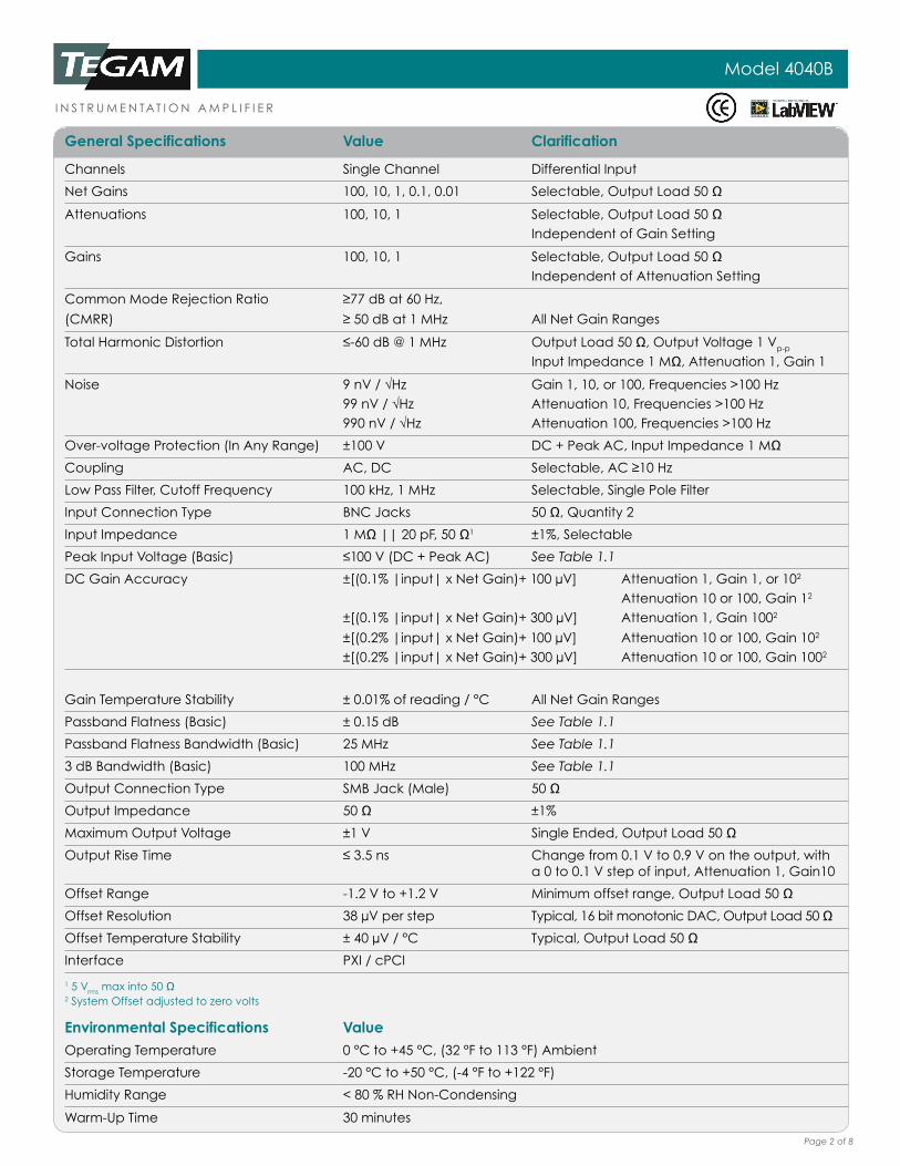
Frequency ResponseAttenuation 10, Gain 1
(Typical Data and Test Limits)
-23.5
-23.0
-22.5
-22.0
-21.5
-21.0
-20.5
-20.0
-19.5
1.00E+06 1.00E+07 1.00E+08
Frequency (Hz)
dB G
ain
1.00 Vp* (Large Signal)
0.70 Vp*
0.40 Vp*
0.10 Vp (Small Signal)
0.07 Vp
0.04 Vp
0.01 Vp
Small Signal Limit
Large Signal Limit
* Empirically Derived Data
Output Voltage
Frequency ResponseAttenuation 100, Gain 1
(Typical Data and Test Limits)
-43.5
-43.0
-42.5
-42.0
-41.5
-41.0
-40.5
-40.0
-39.5
1.00E+06 1.00E+07 1.00E+08
Frequency (Hz)
dB G
ain
1.00 Vp* (Large Signal)
0.70 Vp*
0.40 Vp*
0.10 Vp* (Small Signal)
0.07 Vp*
0.04 Vp*
0.01 Vp
Small Signal Limit
Large Signal Limit
* Empirically Derived Data
Output Voltage
ACCESSORIES DESCRIPTION PART NUMBER
Included Accessories CD Manual 4040B-840
Optional Accessories 1 ft SMB Female to SMB Female Cable CA-3-12 1 ft BNC Male to SMB Female Cable CA-4-12 3 ft BNC Male to SMB Female Cable CA-4-36 3 ft BNC Cable for General Purpose I/O Connections CBL-3102 50 ohm BNC (F-M-F) Tee adapter BNC-3285
Graph 1.1 – 4040B Frequency Response, Attenuation 100, Gain 1
Page 3 of 8
Graph 1.2 – 4040B Frequency Response, Attenuation 10, Gain 1
Model 4040B
I N S T R U M E N TAT I O N A M P L I F I E R
Model 4040B
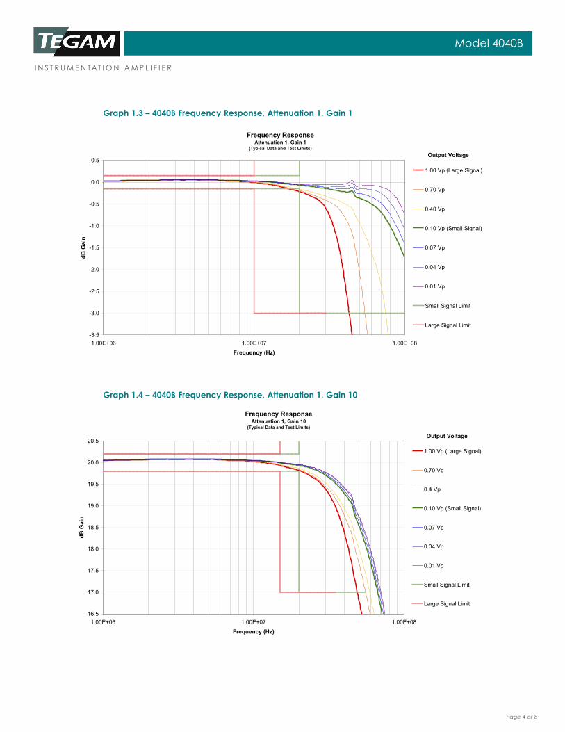
Frequency ResponseAttenuation 1, Gain 1
(Typical Data and Test Limits)
-3.5
-3.0
-2.5
-2.0
-1.5
-1.0
-0.5
0.0
0.5
1.00E+06 1.00E+07 1.00E+08
Frequency (Hz)
dB G
ain
1.00 Vp (Large Signal)
0.70 Vp
0.40 Vp
0.10 Vp (Small Signal)
0.07 Vp
0.04 Vp
0.01 Vp
Small Signal Limit
Large Signal Limit
Output Voltage
Graph 1.3 – 4040B Frequency Response, Attenuation 1, Gain 1
Frequency ResponseAttenuation 1, Gain 10
(Typical Data and Test Limits)
16.5
17.0
17.5
18.0
18.5
19.0
19.5
20.0
20.5
1.00E+06 1.00E+07 1.00E+08
Frequency (Hz)
dB G
ain
1.00 Vp (Large Signal)
0.70 Vp
0.4 Vp
0.10 Vp (Small Signal)
0.07 Vp
0.04 Vp
0.01 Vp
Small Signal Limit
Large Signal Limit
Output Voltage
Graph 1.4 – 4040B Frequency Response, Attenuation 1, Gain 10
Page 4 of 8
Model 4040B
I N S T R U M E N TAT I O N A M P L I F I E R
Model 4040B
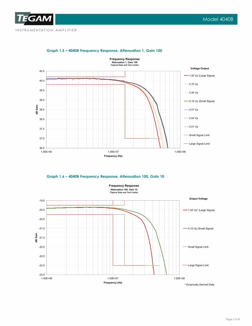
Graph 1.5 – 4040B Frequency Response, Attenuation 1, Gain 100
Frequency ResponseAttenuation 1, Gain 100
(Typical Data and Test Limits)
36.5
37.0
37.5
38.0
38.5
39.0
39.5
40.0
40.5
1.00E+06 1.00E+07 1.00E+08
Frequency (Hz)
dB G
ain
1.00 Vp (Large Signal)
0.70 Vp
0.40 Vp
0.10 Vp (Small Signal)
0.07 Vp
0.04 Vp
0.01 Vp
Small Signal Limit
Large Signal Limit
Voltage Output
Frequency ResponseAttenuation 100, Gain 10
(Typical Data and Test Limits)
-23.5
-23.0
-22.5
-22.0
-21.5
-21.0
-20.5
-20.0
-19.5
1.00E+06 1.00E+07 1.00E+08
Frequency (Hz)
dB G
ain
1.00 Vp* (Large Signal)
0.10 Vp (Small Signal)
Small Signal Limit
Large Signal Limit
* Empirically Derived Data
Output Voltage
Graph 1.6 – 4040B Frequency Response, Attenuation 100, Gain 10
Page 5 of 8
Model 4040B
I N S T R U M E N TAT I O N A M P L I F I E R
Model 4040B
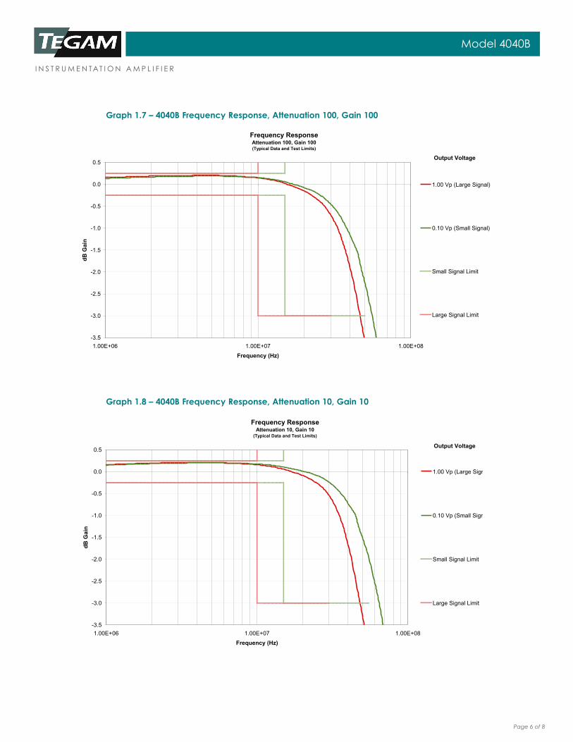
Graph 1.7 – 4040B Frequency Response, Attenuation 100, Gain 100
Graph 1.8 – 4040B Frequency Response, Attenuation 10, Gain 10
Frequency ResponseAttenuation 100, Gain 100(Typical Data and Test Limits)
-3.5
-3.0
-2.5
-2.0
-1.5
-1.0
-0.5
0.0
0.5
1.00E+06 1.00E+07 1.00E+08
Frequency (Hz)
dB G
ain
1.00 Vp (Large Signal)
0.10 Vp (Small Signal)
Small Signal Limit
Large Signal Limit
Output Voltage
Frequency ResponseAttenuation 10, Gain 10
(Typical Data and Test Limits)
-3.5
-3.0
-2.5
-2.0
-1.5
-1.0
-0.5
0.0
0.5
1.00E+06 1.00E+07 1.00E+08
Frequency (Hz)
dB G
ain
1.00 Vp (Large Signal)
0.10 Vp (Small Signal)
Small Signal Limit
Large Signal Limit
Output Voltage
Page 6 of 8
Model 4040B
I N S T R U M E N TAT I O N A M P L I F I E R
Model 4040B
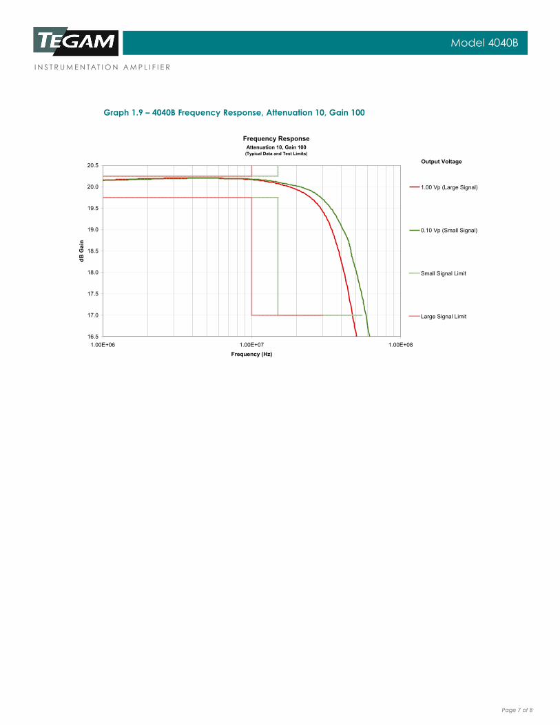
Graph 1.9 – 4040B Frequency Response, Attenuation 10, Gain 100
Frequency ResponseAttenuation 10, Gain 100
(Typical Data and Test Limits)
16.5
17.0
17.5
18.0
18.5
19.0
19.5
20.0
20.5
1.00E+06 1.00E+07 1.00E+08
Frequency (Hz)
dB G
ain
1.00 Vp (Large Signal)
0.10 Vp (Small Signal)
Small Signal Limit
Large Signal Limit
Output Voltage
Page 7 of 8
Model 4040B
I N S T R U M E N TAT I O N A M P L I F I E R
Model 4040B
10 TEGAM Way • Geneva, Ohio 44041
Phone: 440-466-6100 • Fax: 440-466-6110 • E-mail: [email protected] • www.tegam.com
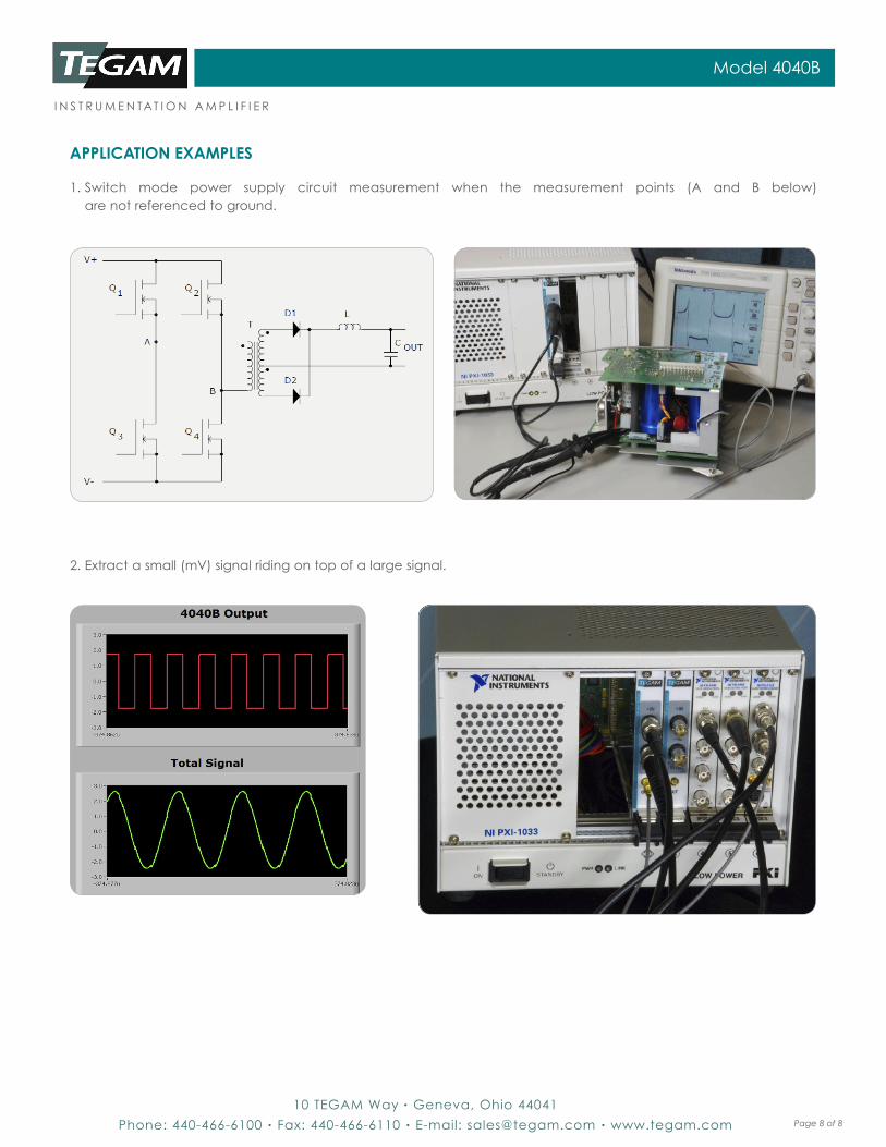
1. Switch mode power supply circuit measurement when the measurement points (A and B below) are not referenced to ground.
APPLICATION EXAMPLES
2. Extract a small (mV) signal riding on top of a large signal.
Page 8 of 8