Embed Size (px)
Citation preview
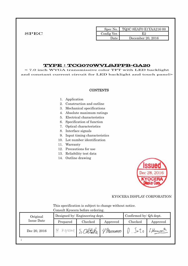
Spec No. TQ3C-8EAF0-E1YAA216-00 SPEC Config Ver. E2
Date December 20, 2016
TYPE : TCG070WVLSJPPB-GA20 < 7.0 inch WVGA transmissive color TFT with LED backlight
and constant current circuit for LED backlight and touch panel>
KYOCERA DISPLAY CORPORATION This specification is subject to change without notice. Consult Kyocera before ordering.
Original Issue Date
Designed by: Engineering dept. Confirmed by: QA dept.
Prepared Checked Approved Checked Approved
Dec 20, 2016
:
CONTENTS 1. Application 2. Construction and outline 3. Mechanical specifications 4. Absolute maximum ratings 5. Electrical characteristics 6. Specification of function 7. Optical characteristics 8. Interface signals 9. Input timing characteristics
10. Lot number identification 11. Warranty 12. Precautions for use 13. Reliability test data 14. Outline drawing
Spec No.
TQ3C-8EAF0-E1YAA216-00 Part No.
TCG070WVLSJPPB-GA20 Page
-
Warning
1. This Kyocera LCD module has been specifically designed for use only in electronic devices and industrial machines in the area of audio control, office automation, industrial control, home appliances, etc. The module should not be used in applications where the highest level of safety and reliability are required and module failure or malfunction of such module results in physical harm or loss of life, as well as enormous damage or loss. Such fields of applications include, without limitation, medical, aerospace, communications infrastructure, atomic energy control. Kyocera expressly disclaims any and all liability resulting in any way to the use of the module in such applications.
2. Customer agrees to indemnify, defend and hold Kyocera harmless
from and against any and all actions, claims, damages, liabilities, awards, costs, and expenses, including legal expenses, resulting from or arising out of Customer's use, or sale for use, or Kyocera modules in applications.
Caution
1. Kyocera shall have the right, which Customer hereby acknowledges, to immediately scrap or destroy tooling for Kyocera modules for which no Purchase Orders have been received from the Customer in a two-year period.
Spec No.
TQ3C-8EAF0-E1YAA216-00 Part No.
TCG070WVLSJPPB-GA20 Page
-
Revision record
Date Designed by : Engineering dept. Confirmed by : QA dept.
Prepared Checked Approved Checked Approved
Rev.No. Date Page Descriptions
Spec No.
TQ3C-8EAF0-E1YAA216-00
Part No.
TCG070WVLSJPPB-GA20
Page
1
M407011
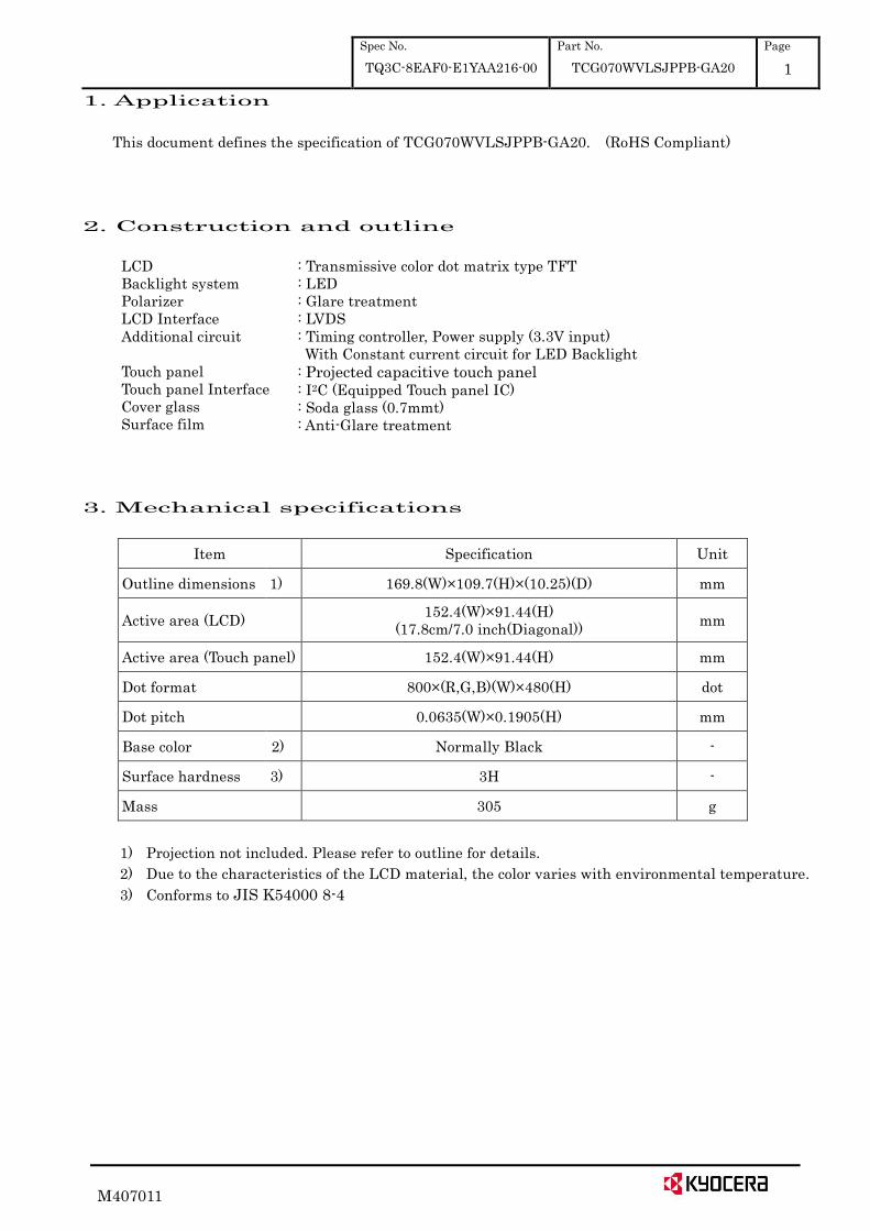
1. Application
This document defines the specification of TCG070WVLSJPPB-GA20. (RoHS Compliant)
2. Construction and outline
LCD Backlight system Polarizer LCD Interface Additional circuit Touch panel Touch panel Interface Cover glass Surface film
: Transmissive color dot matrix type TFT : LED : Glare treatment : LVDS : Timing controller, Power supply (3.3V input) With Constant current circuit for LED Backlight
: Projected capacitive touch panel : I2C (Equipped Touch panel IC) : Soda glass (0.7mmt) : Anti-Glare treatment
3. Mechanical specifications
Item Specification Unit
Outline dimensions 1) 169.8(W)×109.7(H)×(10.25)(D) mm
Active area (LCD) 152.4(W)×91.44(H)
(17.8cm/7.0 inch(Diagonal)) mm
Active area (Touch panel) 152.4(W)×91.44(H) mm
Dot format 800×(R,G,B)(W)×480(H) dot
Dot pitch 0.0635(W)×0.1905(H) mm
Base color 2) Normally Black -
Surface hardness 3) 3H -
Mass 305 g
1) Projection not included. Please refer to outline for details.
2) Due to the characteristics of the LCD material, the color varies with environmental temperature.
3) Conforms to JIS K54000 8-4
Spec No.
TQ3C-8EAF0-E1YAA216-00
Part No.
TCG070WVLSJPPB-GA20
Page
2
M407011
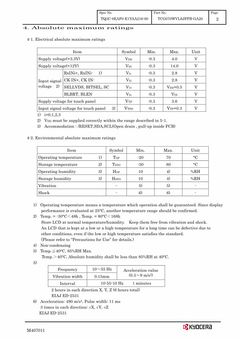
4. Absolute maximum ratings
4-1. Electrical absolute maximum ratings
Item Symbol Min. Max. Unit
Supply voltage(+3.3V) VDD -0.3 4.0 V
Supply voltage(+12V) VIN -0.3 14.0 V
Input signal
voltage 2)
RxINi+, RxINi- 1) VI1 -0.3 2.8 V
CK IN+, CK IN- VI2 -0.3 2.8 V
SELLVDS, BITSEL, SC VI3 -0.3 VDD+0.5 V
BLBRT, BLEN VI4 -0.3 VIN V
Supply voltage for touch panel VTP -0.3 3.6 V
Input signal voltage for touch panel 3) VTPS -0.3 VTP+0.3 V
1) i=0,1,2,3
2) VDD must be supplied correctly within the range described in 5-1.
3) Accommodation : /RESET,SDA,SCL(Open drain , pull-up inside PCB)
4-2. Environmental absolute maximum ratings
Item Symbol Min. Max. Unit
Operating temperature 1) TOP -20 70 °C
Storage temperature 2) TSTO -30 80 °C
Operating humidity 3) HOP 10 4) %RH
Storage humidity 3) HSTO 10 4) %RH
Vibration - 5) 5) -
Shock - 6) 6) -
1) Operating temperature means a temperature which operation shall be guaranteed. Since display
performance is evaluated at 25°C, another temperature range should be confirmed.
2) Temp. = -30°C 48h , Temp. = 80°C 168h
Store LCD at normal temperature/humidity. Keep them free from vibration and shock.
An LCD that is kept at a low or a high temperature for a long time can be defective due to
other conditions, even if the low or high temperature satisfies the standard.
(Please refer to “Precautions for Use” for details.) 4) Non-condensing
5) Temp. 40°C, 85%RH Max.
Temp. 40°C, Absolute humidity shall be less than 85%RH at 40°C.
5)
Frequency 10~55 Hz Acceleration value (0.3~9 m/s2) Vibration width 0.15mm
Interval 10-55-10 Hz 1minutes
2 hours in each direction X, Y, Z (6 hours total)
EIAJ ED-2531
6) Acceleration: 490 m/s2, Pulse width: 11 ms
3 times in each direction: ±X, ±Y, ±Z
EIAJ ED-2531
Spec No.
TQ3C-8EAF0-E1YAA216-00
Part No.
TCG070WVLSJPPB-GA20
Page
3
M407011
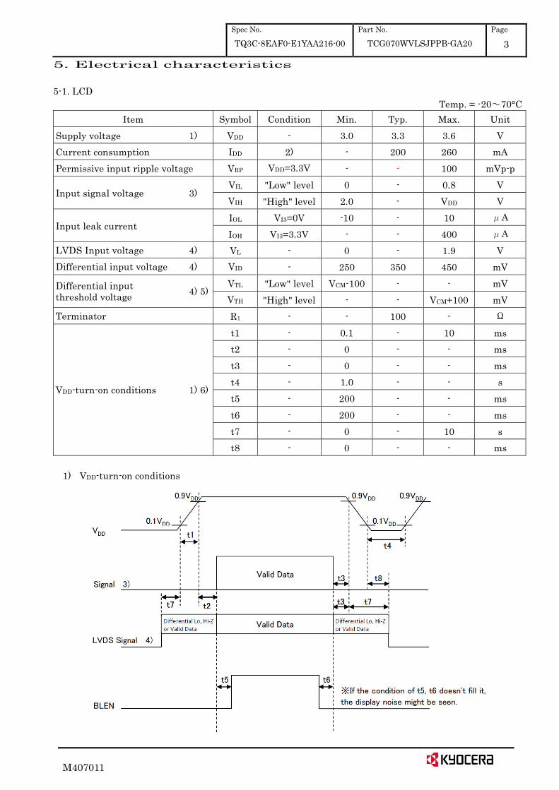
5. Electrical characteristics
5-1. LCD
Temp. = -20~70°C
Item Symbol Condition Min. Typ. Max. Unit
Supply voltage 1) VDD - 3.0 3.3 3.6 V
Current consumption IDD 2) - 200 260 mA
Permissive input ripple voltage VRP VDD=3.3V - - 100 mVp-p
Input signal voltage 3) VIL "Low" level 0 - 0.8 V
VIH "High" level 2.0 - VDD V
Input leak current IOL VI3=0V -10 - 10 μA
IOH VI3=3.3V - - 400 μA
LVDS Input voltage 4) VL - 0 - 1.9 V
Differential input voltage 4) VID - 250 350 450 mV
Differential input threshold voltage
4) 5) VTL "Low" level VCM-100 - - mV
VTH "High" level - - VCM+100 mV
Terminator R1 - - 100 - Ω
VDD-turn-on conditions 1) 6)
t1 - 0.1 - 10 ms
t2 - 0 - - ms
t3 - 0 - - ms
t4 - 1.0 - - s
t5 - 200 - - ms
t6 - 200 - - ms
t7 - 0 - 10 s
t8 - 0 - - ms
1) VDD-turn-on conditions
Spec No.
TQ3C-8EAF0-E1YAA216-00
Part No.
TCG070WVLSJPPB-GA20
Page
4
M407011
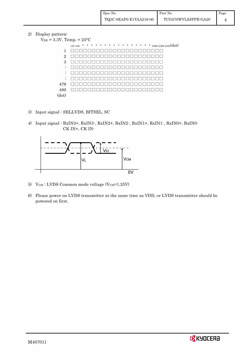
2) Display pattern:
VDD = 3.3V, Temp. = 25°C
123 456 ・・・・・・・・・・・・・・・・2398 2399 2400(dot) 1
2
3
:
:
:
479
480
(dot)
□□□□□□□□□□□□□□□□□□□□□□
□□□□□□□□□□□□□□□□□□□□□□
□□□□□□□□□□□□□□□□□□□□□□
□□□□□□□□□□□□□□□□□□□□□□
□□□□□□□□□□□□□□□□□□□□□□
□□□□□□□□□□□□□□□□□□□□□□
□□□□□□□□□□□□□□□□□□□□□□
□□□□□□□□□□□□□□□□□□□□□□
3) Input signal : SELLVDS, BITSEL, SC
4) Input signal : RxIN3+, RxIN3-, RxIN2+, RxIN2-, RxIN1+, RxIN1-, RxIN0+, RxIN0-
CK IN+, CK IN-
5) VCM : LVDS Common mode voltage (VCM=1.25V)
6) Please power on LVDS transmitter at the same time as VDD, or LVDS transmitter should be
powered on first.
VCM
0V
VL
VID
Spec No.
TQ3C-8EAF0-E1YAA216-00
Part No.
TCG070WVLSJPPB-GA20
Page
5
M407011
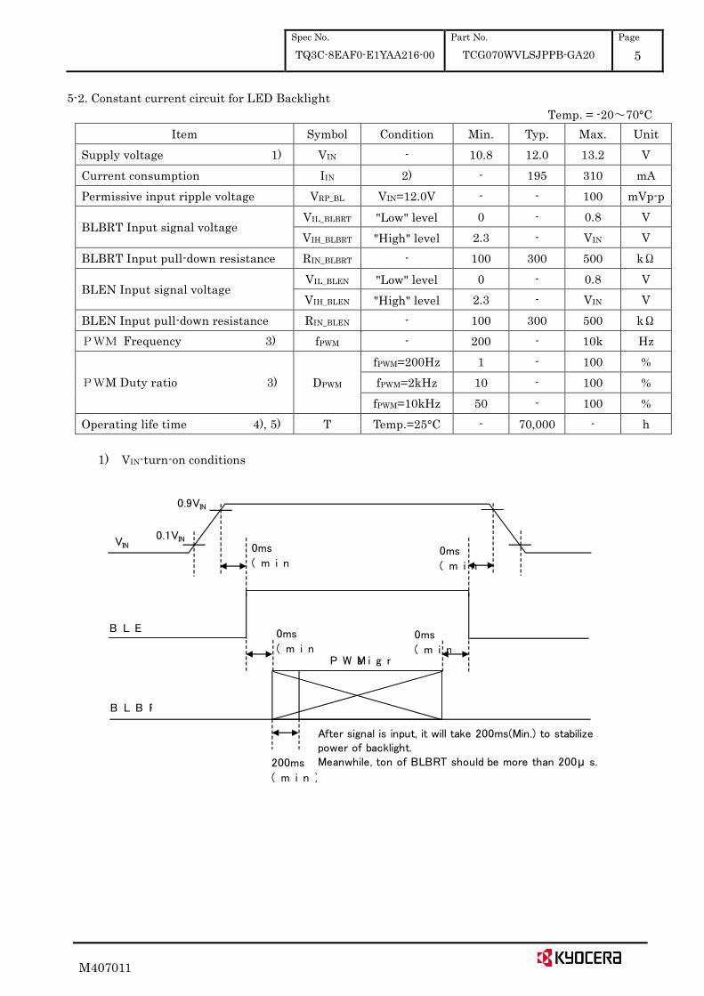
5-2. Constant current circuit for LED Backlight
Temp. = -20~70°C
Item Symbol Condition Min. Typ. Max. Unit
Supply voltage 1) VIN - 10.8 12.0 13.2 V
Current consumption IIN 2) - 195 310 mA
Permissive input ripple voltage VRP_BL VIN=12.0V - - 100 mVp-p
BLBRT Input signal voltage VIL_BLBRT "Low" level 0 - 0.8 V
VIH_BLBRT "High" level 2.3 - VIN V
BLBRT Input pull-down resistance RIN_BLBRT - 100 300 500 kΩ
BLEN Input signal voltage VIL_BLEN "Low" level 0 - 0.8 V
VIH_BLEN "High" level 2.3 - VIN V
BLEN Input pull-down resistance RIN_BLEN - 100 300 500 kΩ
PWM Frequency 3) fPWM - 200 - 10k Hz
PWM Duty ratio 3) DPWM
fPWM=200Hz 1 - 100 %
fPWM=2kHz 10 - 100 %
fPWM=10kHz 50 - 100 %
Operating life time 4), 5) T Temp.=25°C - 70,000 - h
1) VIN-turn-on conditions
After signal is input, it will take 200ms(Min.) to stabilize
power of backlight.
Meanwhile, ton of BLBRT should be more than 200μ s.
0.9VIN
0ms
( m i n
0.1VINVIN
B L E
0ms
( m i n
0ms
( m i n
0ms
( m i n
B L B R
P W Ms i g n
200ms
( m i n )
Spec No.
TQ3C-8EAF0-E1YAA216-00
Part No.
TCG070WVLSJPPB-GA20
Page
6
M407011
2) VIN = 12V, Temp. = 25℃ DPWM = 100%
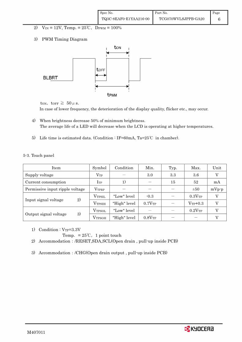
3) PWM Timing Diagram
tON tOFF 50μs.
In case of lower frequency, the deterioration of the display quality, flicker etc., may occur.
4) When brightness decrease 50% of minimum brightness.
The average life of a LED will decrease when the LCD is operating at higher temperatures.
5) Life time is estimated data. (Condition : IF=60mA, Ta=25℃ in chamber).
5-3. Touch panel
Item Symbol Condition Min. Typ. Max. Unit
Supply voltage VTP 3.0 3.3 3.6 V
Current consumption ITP 1) 15 52 mA
Permissive input ripple voltage VTPRP ±50 mVp-p
Input signal voltage 2) VTPSIL "Low" level -0.3 0.3VTP V
VTPSIH "High" level 0.7VTP VTP+0.3 V
Output signal voltage 3) VTPSOL "Low" level 0.2VTP V
VTPSOH "High" level 0.8VTP V
1) Condition : VTP=3.3V
Temp = 25℃ 1 point touch
2) Accommodation:/RESET,SDA,SCL(Open drain , pull-up inside PCB)
3) Accommodation:/CHG(Open drain output , pull-up inside PCB)
Spec No.
TQ3C-8EAF0-E1YAA216-00
Part No.
TCG070WVLSJPPB-GA20
Page
7
M407011
6 Specification of function
Item Description Note
Resolution 800 × 480 -
Starting point upper left 1)
Input 2) finger -
Recommended touch sensor area
φ10.0 mm -
Number of touch point 2 point -
Linearity less than ±2.0mm 3) 4)
Interface I2C -
Device Address 0x4A -
1) Please refer to outline drawing in details.
2) As for input with gloves, separate discussion for feasibility is needed.
3) Performance of linearity is under the environment of no noise.
4) Linearity is not guaranteed. It is for reference only.
5) Structure which has common GND for touch panel and LCD is recommended.
Spec No.
TQ3C-8EAF0-E1YAA216-00
Part No.
TCG070WVLSJPPB-GA20
Page
8
M407011
7. Optical characteristics
Measuring spot =φ6.0mm, Temp. = 25°C
Item Symbol Condition Min. Typ. Max. Unit
Response time Rise τ r θ=φ=0° - 18 - ms
Down τ d θ=φ=0° - 12 - ms
Viewing angle range
View direction
θUPPER
CR 10
- 85 - deg.
θLOWER - 85 -
φLEFT - 85 - deg.
φRIGHT - 85 -
Contrast ratio CR θ=φ=0° 450 650 - -
Brightness L IF=60mA/Line 350 500 - cd/m2
Chromaticity coordinates
Red x
θ=φ=0° 0.550 0.600 0.650
-
y 0.300 0.350 0.400
Green x
θ=φ=0° 0.285 0.335 0.385
y 0.520 0.570 0.620
Blue x
θ=φ=0° 0.100 0.150 0.200
y 0.070 0.120 0.170
White x
θ=φ=0° 0.270 0.320 0.370
y 0.295 0.345 0.395
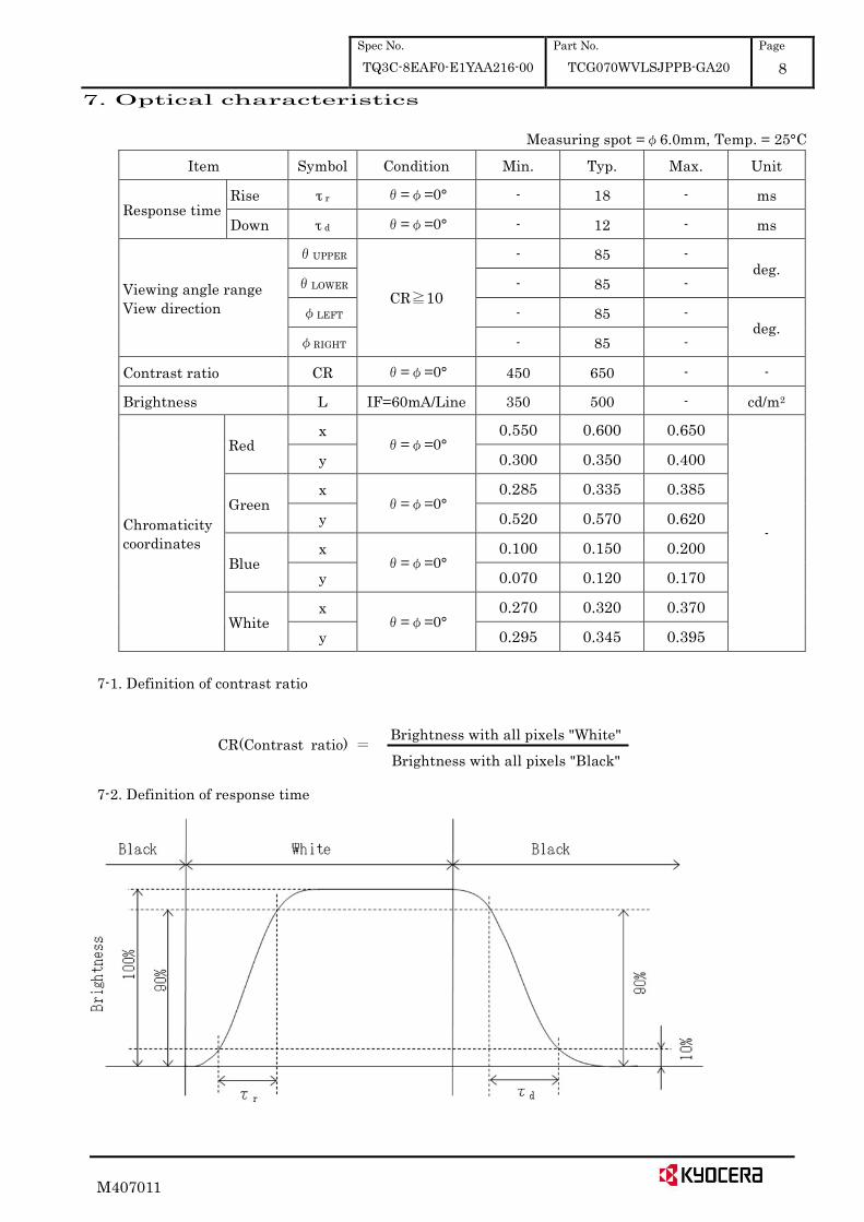
7-1. Definition of contrast ratio
CR(Contrast ratio)
Brightness with all pixels "White"
Brightness with all pixels "Black"
7-2. Definition of response time
Spec No.
TQ3C-8EAF0-E1YAA216-00
Part No.
TCG070WVLSJPPB-GA20
Page
9
M407011
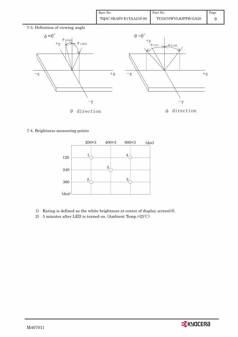
7-3. Definition of viewing angle
7-4. Brightness measuring points
1) Rating is defined as the white brightness at center of display screen(3).
2) 5 minutes after LED is turned on. (Ambient Temp.=25℃)
-x +x
-y
+y
φ=0°
θLOWER
θUPPER
-x +x
-y
θ=0°
φRIGHTφLEFT
θ ”ire“tion φ ”ire“tion
+y
(dot)
(dot)200×3 400×3 600×3
120
240
360
1
2
3
4
5
Spec No.
TQ3C-8EAF0-E1YAA216-00
Part No.
TCG070WVLSJPPB-GA20
Page
10
M407011
8. Interface signals
8-1. Interface signals
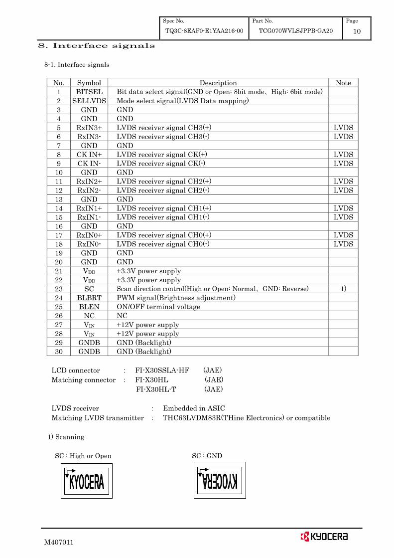
No. Symbol Description Note 1 BITSEL Bit data select signal(GND or Open: 8bit mode、High: 6bit mode) 2 SELLVDS Mode select signal(LVDS Data mapping) 3 GND GND 4 GND GND 5 RxIN3+ LVDS receiver signal CH3(+) LVDS 6 RxIN3- LVDS receiver signal CH3(-) LVDS 7 GND GND 8 CK IN+ LVDS receiver signal CK(+) LVDS 9 CK IN- LVDS receiver signal CK(-) LVDS 10 GND GND 11 RxIN2+ LVDS receiver signal CH2(+) LVDS 12 RxIN2- LVDS receiver signal CH2(-) LVDS 13 GND GND 14 RxIN1+ LVDS receiver signal CH1(+) LVDS 15 RxIN1- LVDS receiver signal CH1(-) LVDS 16 GND GND 17 RxIN0+ LVDS receiver signal CH0(+) LVDS 18 RxIN0- LVDS receiver signal CH0(-) LVDS 19 GND GND 20 GND GND 21 VDD +3.3V power supply 22 VDD +3.3V power supply 23 SC Scan direction control(High or Open: Normal、GND: Reverse) 1) 24 BLBRT PWM signal(Brightness adjustment) 25 BLEN ON/OFF terminal voltage 26 NC NC 27 VIN +12V power supply 28 VIN +12V power supply 29 GNDB GND (Backlight) 30 GNDB GND (Backlight)
LCD connector : FI-X30SSLA-HF (JAE)
Matching connector : FI-X30HL (JAE)
FI-X30HL-T (JAE)
LVDS receiver : Embedded in ASIC
Matching LVDS transmitter : THC63LVDM83R(THine Electronics) or compatible
1) Scanning
SC : High or Open SC : GND
Spec No.
TQ3C-8EAF0-E1YAA216-00
Part No.
TCG070WVLSJPPB-GA20
Page
11
M407011
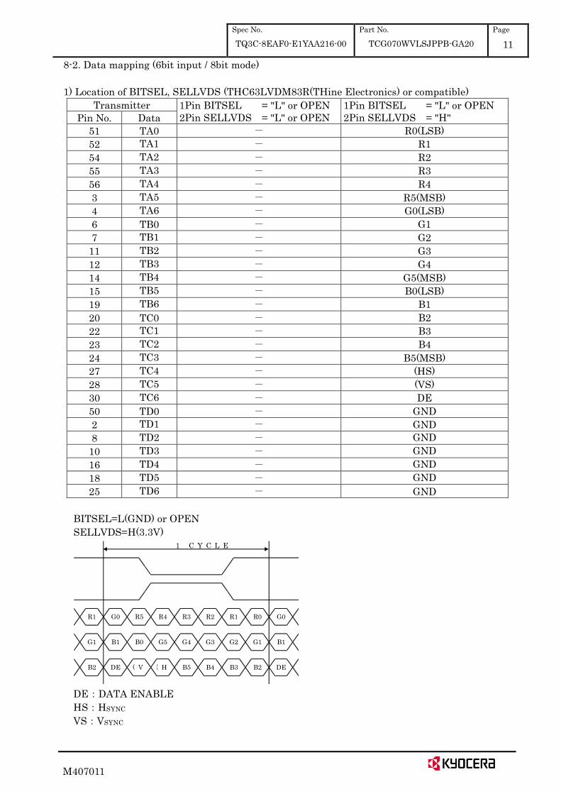
8-2. Data mapping (6bit input / 8bit mode)
1) Location of BITSEL, SELLVDS (THC63LVDM83R(THine Electronics) or compatible)
Transmitter 1Pin BITSEL = "L" or OPEN 2Pin SELLVDS = "L" or OPEN
1Pin BITSEL = "L" or OPEN 2Pin SELLVDS = "H" Pin No. Data
51 TA0 R0(LSB)
52 TA1 R1
54 TA2 R2
55 TA3 R3
56 TA4 R4
3 TA5 R5(MSB)
4 TA6 G0(LSB)
6 TB0 G1
7 TB1 G2
11 TB2 G3
12 TB3 G4
14 TB4 G5(MSB)
15 TB5 B0(LSB)
19 TB6 B1
20 TC0 B2
22 TC1 B3
23 TC2 B4
24 TC3 B5(MSB)
27 TC4 (HS)
28 TC5 (VS)
30 TC6 DE
50 TD0 GND
2 TD1 GND
8 TD2 GND
10 TD3 GND
16 TD4 GND
18 TD5 GND
25 TD6 GND
BITSEL=L(GND) or OPEN
SELLVDS=H(3.3V)
1 C Y C L E
DE( H S B5 B4 B3 B2
G2
B2 DE ( V S )
G1 B1 B0 G1 B1
R4R5 R1 R0 G0
G5 G4 G3
G0R1 R3 R2
DE:DATA ENABLE
HS:HSYNC
VS:VSYNC
Spec No.
TQ3C-8EAF0-E1YAA216-00
Part No.
TCG070WVLSJPPB-GA20
Page
12
M407011
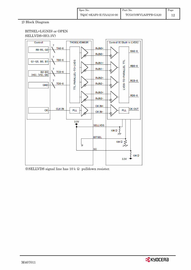
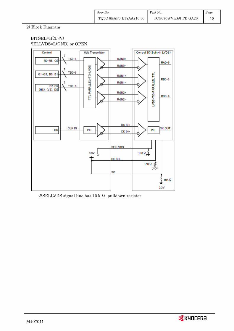
2) Block Diagram
BITSEL=L(GND) or OPEN
SELLVDS=H(3.3V)
※SELLVDS signal line has 10kΩ pulldown resister.
Spec No.
TQ3C-8EAF0-E1YAA216-00
Part No.
TCG070WVLSJPPB-GA20
Page
13
M407011
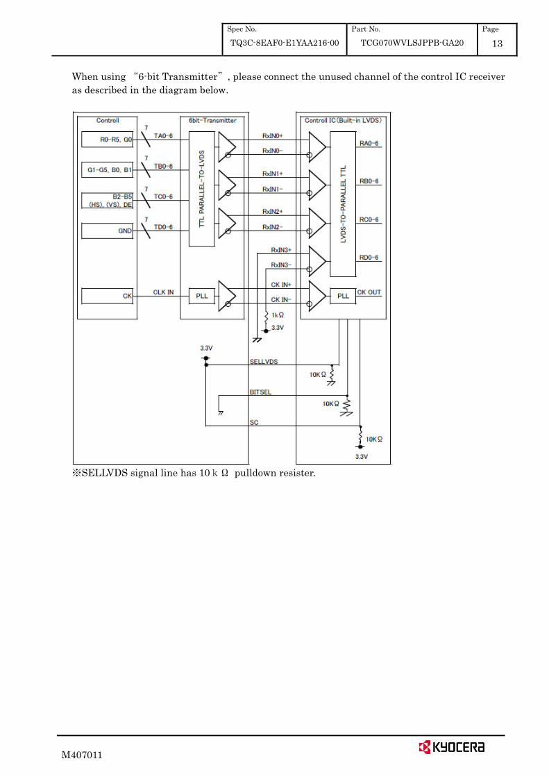
When using 6-bit Transmitter , please connect the unused channel of the control IC receiver
as described in the diagram below.
※SELLVDS signal line has 10kΩ pulldown resister.
Spec No.
TQ3C-8EAF0-E1YAA216-00
Part No.
TCG070WVLSJPPB-GA20
Page
14
M407011
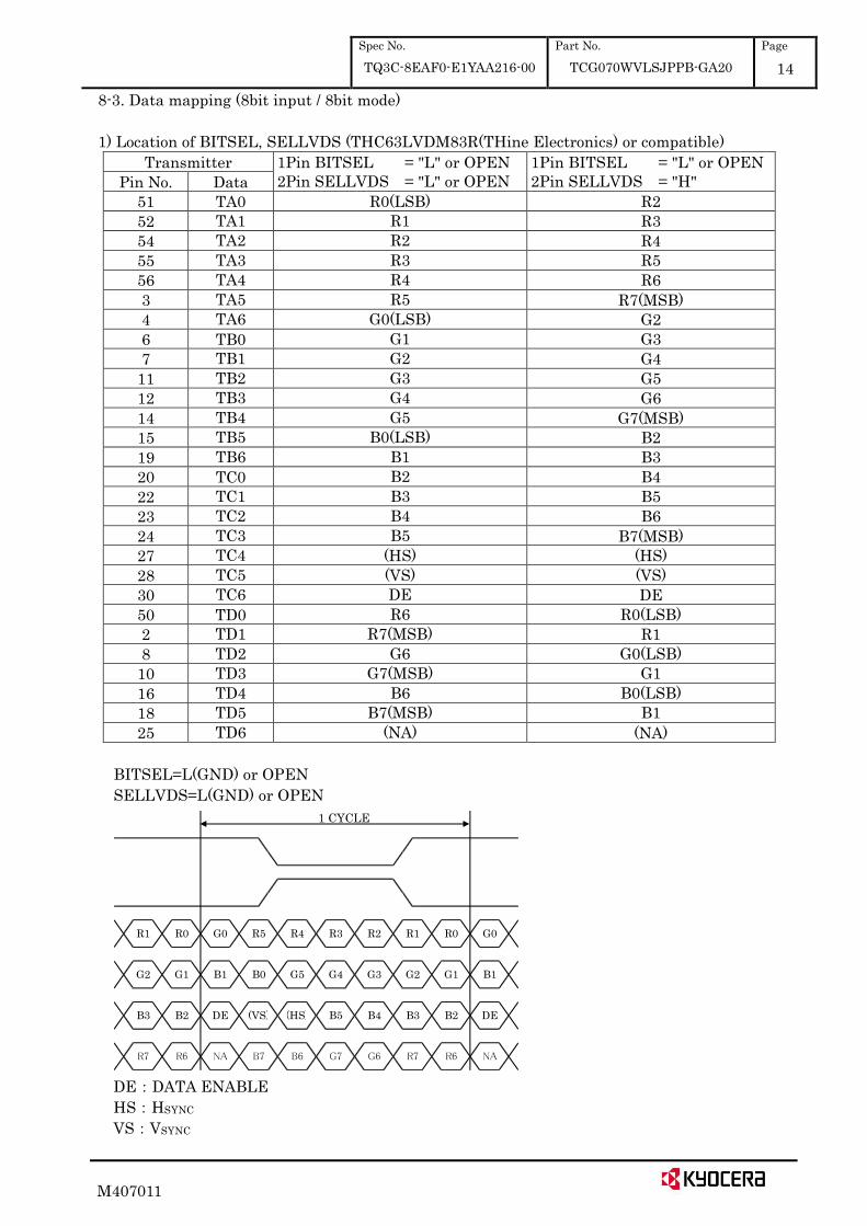
8-3. Data mapping (8bit input / 8bit mode)
1) Location of BITSEL, SELLVDS (THC63LVDM83R(THine Electronics) or compatible)
Transmitter 1Pin BITSEL = "L" or OPEN 2Pin SELLVDS = "L" or OPEN
1Pin BITSEL = "L" or OPEN 2Pin SELLVDS = "H" Pin No. Data
51 TA0 R0(LSB) R2 52 TA1 R1 R3 54 TA2 R2 R4 55 TA3 R3 R5 56 TA4 R4 R6 3 TA5 R5 R7(MSB) 4 TA6 G0(LSB) G2 6 TB0 G1 G3 7 TB1 G2 G4
11 TB2 G3 G5 12 TB3 G4 G6 14 TB4 G5 G7(MSB) 15 TB5 B0(LSB) B2 19 TB6 B1 B3 20 TC0 B2 B4 22 TC1 B3 B5 23 TC2 B4 B6 24 TC3 B5 B7(MSB) 27 TC4 (HS) (HS) 28 TC5 (VS) (VS) 30 TC6 DE DE 50 TD0 R6 R0(LSB) 2 TD1 R7(MSB) R1 8 TD2 G6 G0(LSB)
10 TD3 G7(MSB) G1
16 TD4 B6 B0(LSB)
18 TD5 B7(MSB) B1
25 TD6 (NA) (NA)
BITSEL=L(GND) or OPEN
SELLVDS=L(GND) or OPEN
1 CYCLE
NA
R1
G2
B3
R7 G7 G6 R7 R6R6 NA B7 B6
DE(HS) B5 B4 B3 B2
G2
B2 DE (VS)
G1 B1 B0 G1 B1
R4R5 R1 R0 G0
G5 G4 G3
G0R0 R3 R2
DE:DATA ENABLE
HS:HSYNC
VS:VSYNC
Spec No.
TQ3C-8EAF0-E1YAA216-00
Part No.
TCG070WVLSJPPB-GA20
Page
15
M407011
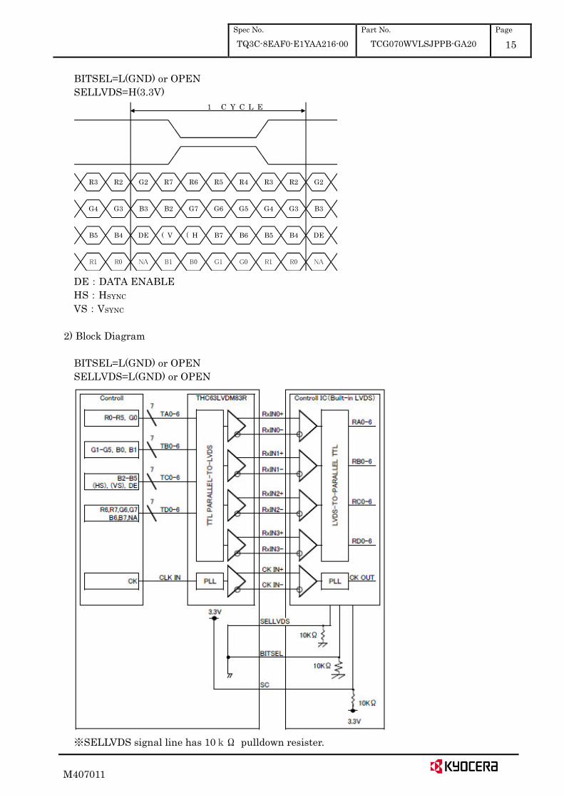
BITSEL=L(GND) or OPEN
SELLVDS=H(3.3V)
1 C Y C L E
R0 G1 G0 R1 R0
R3
G4
B5
R1 NA B1 B0
DE( H S B7 B6 B5 B4
NA
G4
B4 DE ( V S )
G3 B3 B2 G3 B3
R6R7 R3 R2 G2
G7 G6 G5
G2R2 R5 R4
DE:DATA ENABLE
HS:HSYNC
VS:VSYNC
2) Block Diagram
BITSEL=L(GND) or OPEN
SELLVDS=L(GND) or OPEN
※SELLVDS signal line has 10kΩ pulldown resister.
Spec No.
TQ3C-8EAF0-E1YAA216-00
Part No.
TCG070WVLSJPPB-GA20
Page
16
M407011
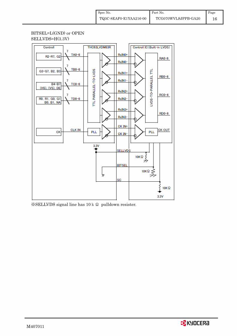
BITSEL=L(GND) or OPEN
SELLVDS=H(3.3V)
※SELLVDS signal line has 10kΩ pulldown resister.
Spec No.
TQ3C-8EAF0-E1YAA216-00
Part No.
TCG070WVLSJPPB-GA20
Page
17
M407011
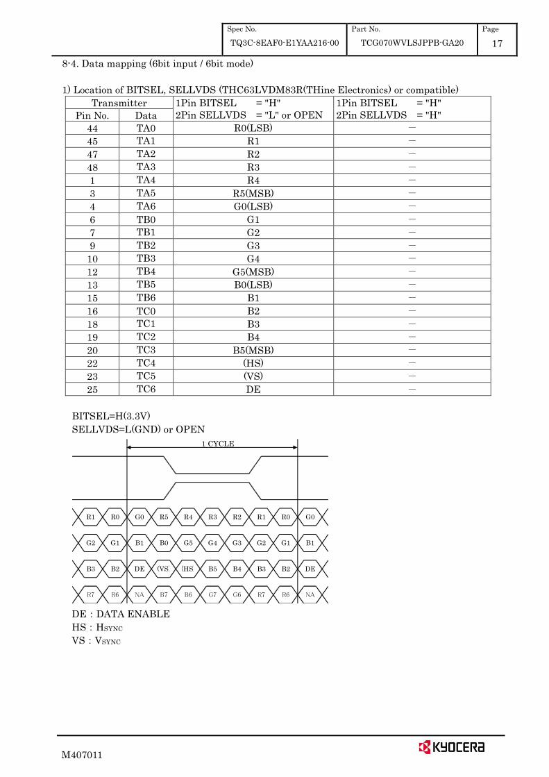
8-4. Data mapping (6bit input / 6bit mode)
1) Location of BITSEL, SELLVDS (THC63LVDM83R(THine Electronics) or compatible)
Transmitter 1Pin BITSEL = "H" 2Pin SELLVDS = "L" or OPEN
1Pin BITSEL = "H" 2Pin SELLVDS = "H" Pin No. Data
44 TA0 R0(LSB)
45 TA1 R1
47 TA2 R2
48 TA3 R3
1 TA4 R4
3 TA5 R5(MSB)
4 TA6 G0(LSB)
6 TB0 G1
7 TB1 G2
9 TB2 G3
10 TB3 G4
12 TB4 G5(MSB)
13 TB5 B0(LSB)
15 TB6 B1
16 TC0 B2
18 TC1 B3
19 TC2 B4
20 TC3 B5(MSB)
22 TC4 (HS)
23 TC5 (VS)
25 TC6 DE
BITSEL=H(3.3V)
SELLVDS=L(GND) or OPEN
1 CYCLE
NA
R1
G2
B3
R7 G7 G6 R7 R6R6 NA B7 B6
DE(HS) B5 B4 B3 B2
G2
B2 DE (VS)
G1 B1 B0 G1 B1
R4R5 R1 R0 G0
G5 G4 G3
G0R0 R3 R2
DE:DATA ENABLE
HS:HSYNC
VS:VSYNC
Spec No.
TQ3C-8EAF0-E1YAA216-00
Part No.
TCG070WVLSJPPB-GA20
Page
18
M407011
2) Block Diagram
BITSEL=H(3.3V)
SELLVDS=L(GND) or OPEN
※SELLVDS signal line has 10kΩ pulldown resister.
Spec No.
TQ3C-8EAF0-E1YAA216-00
Part No.
TCG070WVLSJPPB-GA20
Page
19
M407011
8-5 Touch panel
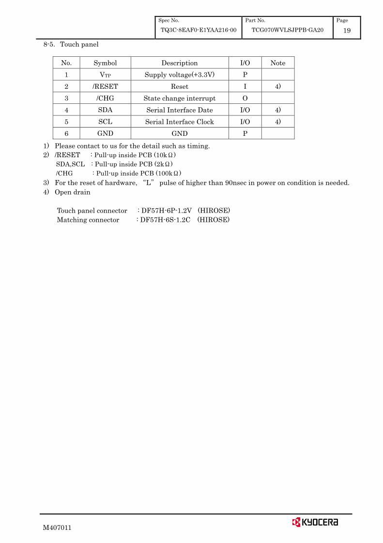
1) Please contact to us for the detail such as timing.
2) /RESET : Pull-up inside PCB (10kΩ)
SDA,SCL : Pull-up inside PCB (2kΩ)
/CHG : Pull-up inside PCB (100kΩ)
3) For the reset of hardware, L pulse of higher than 90nsec in power on condition is needed.
4) Open drain
Touch panel connector : DF57H-6P-1.2V (HIROSE)
Matching connector : DF57H-6S-1.2C (HIROSE)
No. Symbol Description I/O Note
1 VTP Supply voltage(+3.3V) P
2 /RESET Reset I 4)
3 /CHG State change interrupt O
4 SDA Serial Interface Date I/O 4)
5 SCL Serial Interface Clock I/O 4)
6 GND GND P
Spec No.
TQ3C-8EAF0-E1YAA216-00
Part No.
TCG070WVLSJPPB-GA20
Page
20
M407011
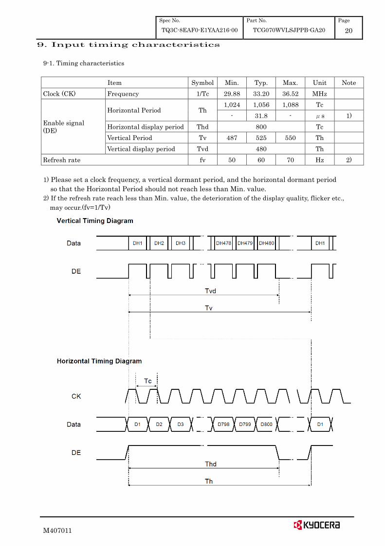
9. Input timing characteristics
9-1. Timing characteristics
Item Symbol Min. Typ. Max. Unit Note
Clock (CK) Frequency 1/Tc 29.88 33.20 36.52 MHz
Enable signal (DE)
Horizontal Period Th 1,024 1,056 1,088 Tc
- 31.8 - μs 1)
Horizontal display period Thd 800 Tc
Vertical Period Tv 487 525 550 Th
Vertical display period Tvd 480 Th
Refresh rate fv 50 60 70 Hz 2)
1) Please set a clock frequency, a vertical dormant period, and the horizontal dormant period
so that the Horizontal Period should not reach less than Min. value.
2) If the refresh rate reach less than Min. value, the deterioration of the display quality, flicker etc.,
may occur.(fv=1/Tv)
Spec No.
TQ3C-8EAF0-E1YAA216-00
Part No.
TCG070WVLSJPPB-GA20
Page
21
M407011
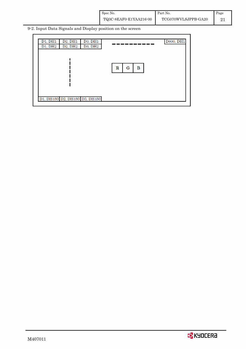
9-2. Input Data Signals and Display position on the screen
Spec No.
TQ3C-8EAF0-E1YAA216-00
Part No.
TCG070WVLSJPPB-GA20
Page
22
M407011
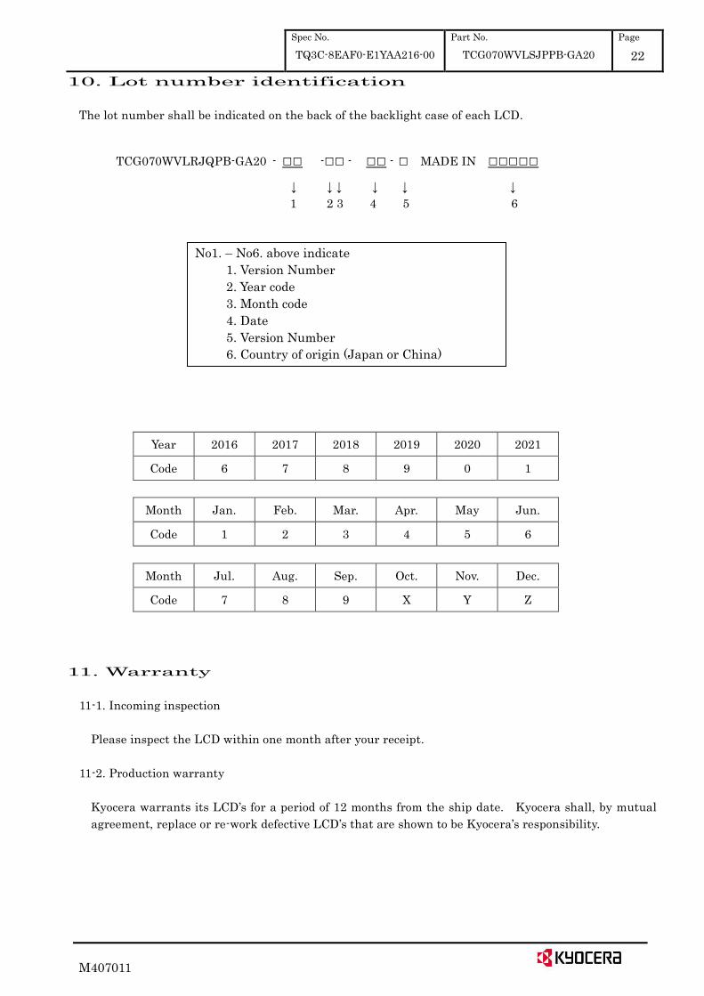
10. Lot number identification
The lot number shall be indicated on the back of the backlight case of each LCD.
TCG070WVLRJQPB-GA20 - □□ -□□ - □□ - □ MADE IN □□□□□
↓ ↓ ↓ ↓ ↓ ↓
1 2 3 4 5 6
Year 2016 2017 2018 2019 2020 2021
Code 6 7 8 9 0 1
Month Jan. Feb. Mar. Apr. May Jun.
Code 1 2 3 4 5 6
Month Jul. Aug. Sep. Oct. Nov. Dec.
Code 7 8 9 X Y Z
11. Warranty
11-1. Incoming inspection
Please inspect the LCD within one month after your receipt.
11-2. Production warranty
Kyocera warrants its LCD’s for a period of 12 months from the ship date. Kyocera shall, by mutual agreement, replace or re-work defective LCD’s that are shown to be Kyocera’s responsibility.
No1. – No6. above indicate
1. Version Number
2. Year code
3. Month code
4. Date
5. Version Number
6. Country of origin (Japan or China)
Spec No.
TQ3C-8EAF0-E1YAA216-00
Part No.
TCG070WVLSJPPB-GA20
Page
23
M407011
12. Precautions for use
12-1. Installation of the LCD 1) The product shall be installed so that there is no pressure on the LSI chips. 2) When LCD is installed, power shall be put off. Same applies to plug in/out of FFC/FPC/Cable. 3) When handling connector, please do not make any excessive pressure than needed. It may
damage the LCD. 4) Since this product is wide viewing product, occurrence level of in-plane unevenness by the external
stress is different compared to current normal viewing product. So there is a possibility that in-plane unevenness will be occurred by over twist, strain giving by attaching to LCD, and over pressure to touch panel. Please be careful of stress when designing the housing.
5) A transparent protection sheet is attached to the touch panel. Please remove the protection film slowly before use, paying attention to static electricity.
6) Touch location is detected by the change of capacitance. Therefore, if there is any factor close to LCD which may change electric field, malfunction may be caused as it may give adverse effect on coordinate detecting mechanism.
7) When designing your case, using material composed with insulating resin is recommended
for bezel of touch panel. When metal plate is used, malfunction may be caused by the
occurrence of capacitance coupling on the periphery of active area. 8) The Bezel on the upper part of Touch-Panel recommends using the material which consists of
"Insulating Resin", when designing the housing. Otherwise, Malfunction may be caused by occurring "capacitive coupling with sheet metal" in the perimeter part of active area if sheet metal is used.
12-2. Static electricity 1) Since CMOS ICs are mounted directly onto the LCD glass, protection from static electricity is
required. 2) Workers should use body grounding. Operator should wear ground straps.
12-3. LCD operation
1) The product shall be operated within the limits specified. Operation at values outside of these
limits may shorten life, and/or harm display images.
2) This product shall be operated in the atmosphere free from high temperature, high humidity,
condensation and chemical atmospheres such as salt, acid and alkaline, which may cause gas
corrosion, in order to prevent damage of this product and electrification.
3) Please select the best display pattern based on your evaluation because flicker, lines or
nonuniformity or unevenness can be visible depending on display patterns.
4) There is possibility to cause malfunction by using the touch panel with droplets or conductive
this product on the surface of touch panel, please design the software with having discussion
between both companies. 5) It is simulated that input for this product will be done by fingers. Please let us know if the
input will be done except by fingers since it needs to change the setting.
12-4. Storage
1) The product shall be stored within the temperature and humidity limits specified.
Store in a dark area, and protect the product from direct sunlight or fluorescent light. 2) Always store the product so that it is free from external pressure onto it. 3) Please store the product board in a location that is free of dust, corrosive elements, or
environmental gas (such as acid and alkali salts).
Spec No.
TQ3C-8EAF0-E1YAA216-00
Part No.
TCG070WVLSJPPB-GA20
Page
24
M407011
12-5. Usage
1) DO NOT store in a high humidity environment for extended periods. Polarizer degradation bubbles,
and/or peeling off of the polarizer may result.
2) Do not push or rub the panel's surface with hard to sharp objects such as knives, or the touch panel
may be scratched.
3) In case a surface of touch panel gets dirty, please wipe gently with soft cotton by soaking in a
neutral detergent or small amount of ethyl alcohol. Please exercise caution in when handling
hazardous chemicals.
4) The product is made of glass. It may break when dropped, or vibrated excessively. Usually there is
a film on the surface of the glass which would prevent broken glass from scattering, but
nevertheless handle it carefully during assembly and treat it gently during use. Please take extra
caution to the edge due to less strength than surface can cause glass to break.
5) Please implement protective countermeasures against high voltage surges such as lightning strikes.
Damaged may be caused by abnormal voltage.
6) The product is not designed as anti-radiation product.
7) Always keep the product free from condensation during testing. Malfunction of touch panel may be
caused. Condensation may permanently spot or stain the polarizer and film.
8) Do not make over circuit board because it will result in damage.
9) This product has been specifically designed for use in general electronic devices, but not for use in
a special environment such as usage in an active gas. Hence, when the product is supposed to be
used in a special environment, evaluate the product thoroughly beforehand and do not expose the
product to chemicals such as an active gas.
10) Please do not use solid-base image pattern for long hours because a temporary afterimage may
appear. We recommend using screen saver etc. in cases where a solid-base image pattern must be
used.
11) Liquid crystal may leak when the product is broken. Be careful not to let the fluid go into your eyes
and mouth. In the case the fluid touches your body; rinse it off right away with water and soap.
Spec No.
TQ3C-8EAF0-E1YAA216-00
Part No.
TCG070WVLSJPPB-GA20
Page
25
M407011
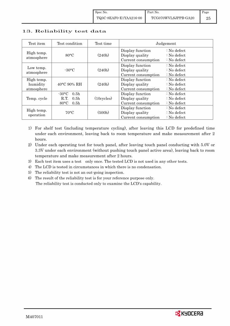
13. Reliability test data
Test item Test condition Test time Judgement
High temp. atmosphere
80°C (240h) Display function Display quality Current consumption
: No defect : No defect : No defect
Low temp. atmosphere
-30°C (240h) Display function Display quality Current consumption
: No defect : No defect : No defect
High temp. humidity
atmosphere 40°C 90% RH (240h)
Display function Display quality Current consumption
: No defect : No defect : No defect
Temp. cycle -30°C
R.T. 80°C
0.5h 0.5h 0.5h
(10cycles) Display function Display quality Current consumption
: No defect : No defect : No defect
High temp. operation
70°C (500h) Display function Display quality Current consumption
: No defect : No defect : No defect
1) For shelf test (including temperature cycling), after leaving this LCD for predefined time
under each environment, leaving back to room temperature and make measurement after 2
hours.
2) Under each operating test for touch panel, after leaving touch panel conducting with 5.0V or
3.3V under each environment (without pushing touch panel active area), leaving back to room
temperature and make measurement after 2 hours.
3) Each test item uses a test only once. The tested LCD is not used in any other tests.
4) The LCD is tested in circumstances in which there is no condensation.
5) The reliability test is not an out-going inspection.
6) The result of the reliability test is for your reference purpose only.
The reliability test is conducted only to examine the LCD's capability.
Spec No. TQ3C-8EAF0-E2YAA216-00
Config Ver. E2
Date December 20, 2016
KYOCERA INSPECTION STANDARD
TYPE : TCG070WVLSJPPB-GA20
KYOCERA DISPLAY CORPORATION
Original
Issue Date
Designed by : Engineering dept. Confirmed by : QA dept.
Prepared Checked Approved Checked Approved
Dec 20, 2016
Spec No.
TQ3C-8EAF0-E2YAA216-00
Part No.
TCG070WVLSJPPB-GA20
Page
-
Revision record
Date Designed by : Engineering dept. Confirmed by : QA dept.
Prepared Checked Approved Checked Approved
Rev.No. Date Page Descriptions
Spec No.
TQ3C-8EAF0-E2YAA216-00
Part No.
TCG070WVLSJPPB-GA20
Page
1
Visuals specification
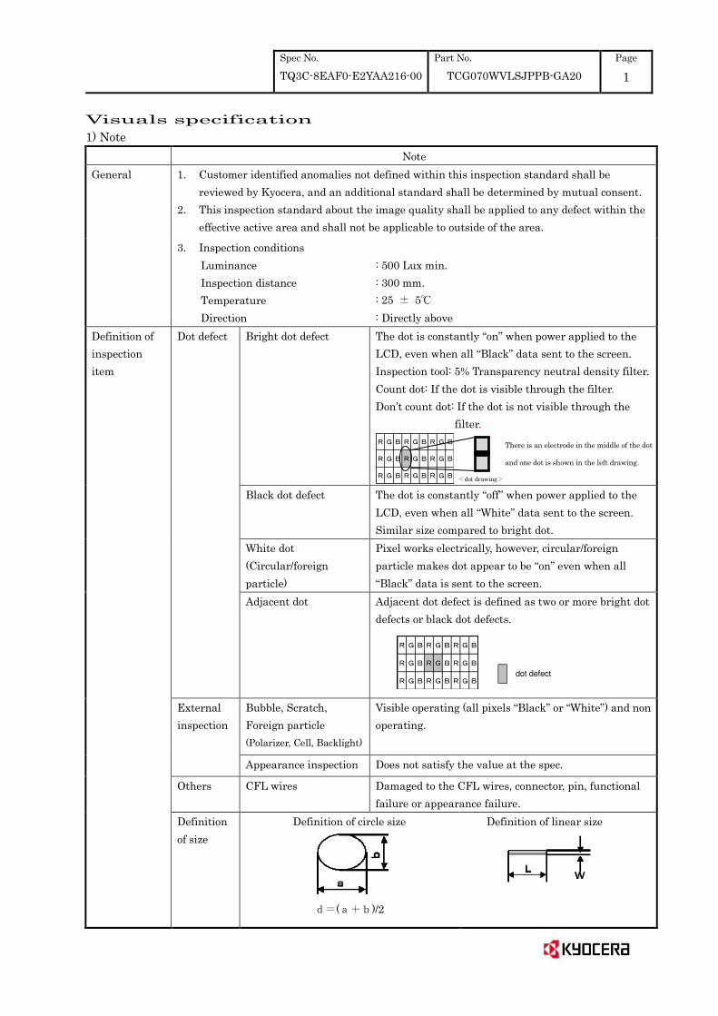
1) Note
Note
General 1. Customer identified anomalies not defined within this inspection standard shall be
reviewed by Kyocera, and an additional standard shall be determined by mutual consent.
2. This inspection standard about the image quality shall be applied to any defect within the
effective active area and shall not be applicable to outside of the area.
3. Inspection conditions
Luminance
Inspection distance
Temperature
Direction
: 500 Lux min.
: 300 mm.
: 25 ± 5℃
: Directly above
Definition of
inspection
item
Dot defect Bright dot defect The dot is constantly “on” when power applied to the
LCD, even when all “Black” data sent to the screen.
Inspection tool: 5% Transparency neutral density filter.
Count dot: If the dot is visible through the filter.
Don’t count dot: If the dot is not visible through the
filter.
R G B R G B R G B
R G B R G B R G B
R G B R G B R G B
Black dot defect
The dot is constantly “off” when power applied to the
LCD, even when all “White” data sent to the screen.
Similar size compared to bright dot.
White dot
(Circular/foreign
particle)
Pixel works electrically, however, circular/foreign
particle makes dot appear to be “on” even when all “Black” data is sent to the screen.
Adjacent dot Adjacent dot defect is defined as two or more bright dot
defects or black dot defects.
R G B R G B R G B
R G B R G B R G B
R G B R G B R G B
dot defect
External
inspection
Bubble, Scratch,
Foreign particle
(Polarizer, Cell, Backlight)
Visible operating (all pixels “Black” or “White”) and non
operating.
Appearance inspection Does not satisfy the value at the spec.
Others CFL wires Damaged to the CFL wires, connector, pin, functional
failure or appearance failure.
Definition
of size
Definition of circle size
d ( + )/2
Definition of linear size
dot drawing
There is an electrode in the middle of the dot
and one dot is shown in the left drawing.
Spec No.
TQ3C-8EAF0-E2YAA216-00
Part No.
TCG070WVLSJPPB-GA20
Page
2
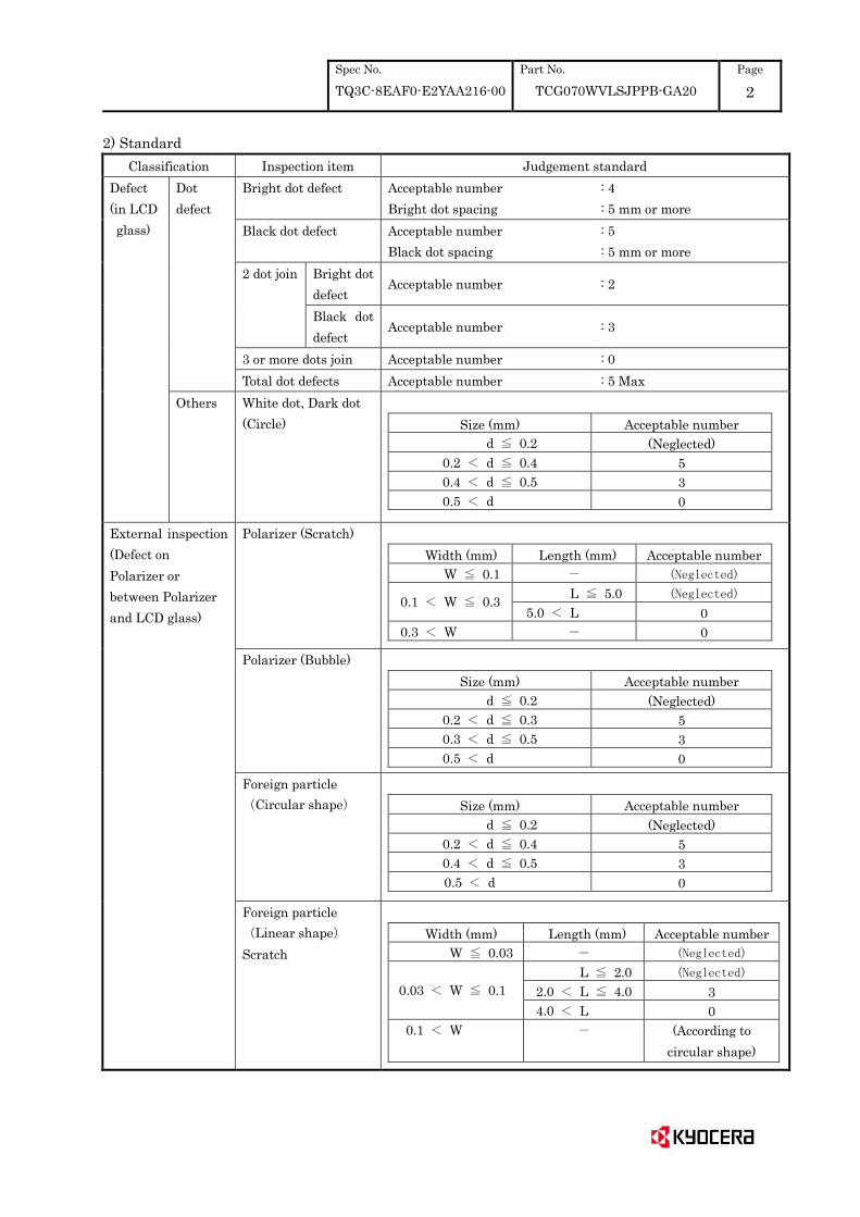
2) Standard
Classification Inspection item Judgement standard
Defect
(in LCD
glass)
Dot
defect
Bright dot defect Acceptable number
Bright dot spacing
: 4
: 5 mm or more
Black dot defect Acceptable number
Black dot spacing
: 5
: 5 mm or more
2 dot join Bright dot
defect Acceptable number : 2
Black dot
defect Acceptable number : 3
3 or more dots join Acceptable number : 0
Total dot defects Acceptable number : 5 Max
Others White dot, Dark dot
(Circle)
Size (mm) Acceptable number
0.2 d ≦ 0.2 (Neglected)
0.2 d ≦ 0.4 5
0.4 d ≦ 0.5 3
0.5 d ≦ 0.4 0
External inspection
(Defect on
Polarizer or
between Polarizer
and LCD glass)
Polarizer (Scratch)
Width (mm) Length (mm) Acceptable number
0.1 W ≦ 0.1 - (Neglected)
0.1 W ≦ 0.3 2.0 L ≦ 5.0 (Neglected)
5.0 L ≦ 5.0 0
0.3 W ≦ 0.3 - 0
Polarizer (Bubble)
Size (mm) Acceptable number
0.2 d ≦ 0.2 (Neglected)
0.2 d ≦ 0.3 5
0.3 d ≦ 0.5 3
0.5 d ≦ 0.4 0
Foreign particle
Circular shape
Size (mm) Acceptable number
0.2 d ≦ 0.2 (Neglected)
0.2 d ≦ 0.4 5
0.4 d ≦ 0.5 3
0.5 d ≦0 .4 0
Foreign particle
Linear shape
Scratch
Width (mm) Length (mm) Acceptable number
0.00 W ≦ 0.03 - (Neglected)
0.03 W ≦ 0.10
2.0 L ≦ 2.0 (Neglected)
2.0 L ≦ 4.0 3
4.0 L ≦ 5.0 0
0.1 W ≦0.3 - (According to
circular shape)
Spec No.
TQ3C-8EAF0-E2YAA216-00
Part No.
TCG070WVLSJPPB-GA20
Page
3
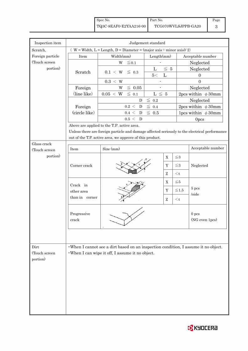
Inspection item Judgement standard
Scratch,
Foreign particle
(Touch screen
portion)
W = Width, L = Length, D = Diameter = (major axis+minor axis)/ 2
Item Width(mm) Length(mm) Acceptable number
Scratch
W ≦0.1 - Neglected
0.1 W ≦ 0.3 L ≦ 5 Neglected
5 L 0
0.3 W - 0
Foreign
line like
W ≦ 0.05 - Neglected
0.05 W ≦ 0.1 L ≦ 5 2pcs within φ30mm
Foreign
(circle like
D ≦ 0.2 Neglected
0.2 D ≦ 0.4 2pcs within φ30mm
0.4 D ≦ 0.5 1pcs within φ30mm
0.5 D 0pcs
Above are applied to the T.P. active area.
Unless there are foreign particle and damage affected seriously to the electrical performance
out of the T.P. active area, we approve of this product.
Glass crack
(Touch screen
portion)
Item Size (mm) Acceptable number
Corner crack
X ≦3
Neglected Y ≦3
Z t
Crack in
other area
than in corner
X ≦5
5 pcs
/side Y ≦1.5
Z t
Progressive
crack
.
0 pcs
(NG even 1pcs)
Dirt
(Touch screen
portion)
・When I cannot see a dirt based on an inspection condition, I assume it no object.
・When I can wipe it off, I assume it no object.