Embed Size (px)
Citation preview

DA7212
Datasheet/Ultra-low power stereo codec Company confidential
Datasheet Revision 3a 19 August 2014
CFR0011-120-00 Rev 4 1 of 154 © 2014 Dialog Semiconductor GmbH
General description
DA7212 is an ultra-low power audio codec targeting portable audio devices. The input paths support stereo FM line input and up to four analogue (or two analogue and two digital) microphones with two independent microphone biases. Comprehensive analogue mixing and bypass paths to the output drivers are available.
The headphone output is true-ground Class G with integrated charge pump. There is also a differential Class AB speaker driver that can serve as a mono lineout.
Digital audio transfer to/from the external processor is via a bidirectional digital audio interface that supports all common sample rates and formats. The device may be operated in slave or master modes using the internal PLL which may be bypassed if not required.
To fully optimise each customer application, a range of built in filtering, equalisation and audio enhancements are available. These are accessible by the processor over the I2C serial interface.
Key features
100 dB SNR stereo audio playback into 16 - 32 Ω headphones
3.1 mW power consumption for stereo DAC to headphone playback
1.2 W mono speaker driver
650 µW mono voice record
Stereo digital microphone support
Supports up to four analogue microphones
Two low-noise microphone-bias outputs
Low-power PLL provides system clocking and audio sample rate flexibility
Built-in 5-band equaliser, ALC and noise-gate functions
Built-in beep generator
Integrated system controller to eliminate pops and clicks
Minimised external component count
34-ball WLCSP (4.54 mm x 1.66 mm) package
Staggered 0.5 mm pitch for easy PCB routing
Applications
Personal Media Players
Audio headphone/headsets
Wearables
Embedded applications
Arduino-compatible development systems
Figure 1: The DA7212 chip

DA7212
Datasheet/Ultra-low power stereo codec Company confidential
Datasheet Revision 3a 19 August 2014
CFR0011-120-00 Rev 4 2 of 154 © 2014 Dialog Semiconductor GmbH
Contents
General description .................................................................................................................... 1
Key features ............................................................................................................................... 1
Applications ............................................................................................................................... 1
Contents .................................................................................................................................... 2
Figures ....................................................................................................................................... 6
Tables ........................................................................................................................................ 7
1 Terms and definitions ........................................................................................................... 9
2 Block diagram ......................................................................................................................10
3 Pinout .................................................................................................................................11
4 Absolute maximum ratings ..................................................................................................14
5 Recommended operating conditions ....................................................................................15
6 Electrical characteristics .......................................................................................................16
7 Parametric specifications .....................................................................................................17
8 Digital signal processing .......................................................................................................20
9 Audio outputs ......................................................................................................................23
11 Clock generation ..................................................................................................................27
12 Phase Locked Loop (PLL) ......................................................................................................27
13 Digital interfaces..................................................................................................................28
Codec Start-Up Time ........................................................................................................... 31 13.1
14 Functional description .........................................................................................................32
General description............................................................................................................. 32 14.1
Input Signal Chain ............................................................................................................... 32 14.2
Microphone Inputs ............................................................................................................. 33 14.3
Digital microphones ............................................................................................................ 34 14.4
Auxiliary inputs ................................................................................................................... 35 14.5
Input mixers ........................................................................................................................ 35 14.6
Stereo audio ADC ................................................................................................................ 36 14.7
Automatic Level Control (ALC) ............................................................................................ 36 14.8

DA7212
Datasheet/Ultra-low power stereo codec Company confidential
Datasheet Revision 3a 19 August 2014
CFR0011-120-00 Rev 4 3 of 154 © 2014 Dialog Semiconductor GmbH
Beep Generator and Controller .......................................................................................... 38 14.9
Output Signal Chain ............................................................................................................ 39 14.10
Stereo Audio DAC ................................................................................................................ 40 14.11
Output Mixer ...................................................................................................................... 40 14.12
Headphone Amplifier .......................................................................................................... 41 14.13
Speaker Amplifier ................................................................................................................ 41 14.14
Charge Pump Control .......................................................................................................... 42 14.15
Charge pump clock control ................................................................................................. 44 14.16
Boosting the charge pump using demand feedback control .............................................. 44 14.17
Tracking the demands on the charge pump output ............................................. 44 14.17.1
14.17.1.1 CP_MCHANGE = 00 (manual mode) .................................................. 44
14.17.1.2 CP_MCHANGE = 01 (tracking the PGA gain setting) .......................... 44
14.17.1.3 CP_MCHANGE = 10 (tracking the DAC signal setting) ........................ 44
14.17.1.4 CP_MCHANGE = 11 (tracking the output signal magnitude) ............. 44
Specifying clock frequencies when tracking the charge pump output 14.17.2
demand ................................................................................................................. 45
Controlling the boost of the charge pump clock-frequency ................................ 45 14.17.3
14.17.3.1 CP_ANALOGUE_LVL = 01 ................................................................... 45
14.17.3.2 CP_ANALOGUE_LVL = 10 ................................................................... 45
Other Charge Pump Controls .............................................................................................. 46 14.18
Digital Signal Processing Engine .......................................................................................... 46 14.19
Variable High Pass Audio Filter (DC Cut) ............................................................................. 47 14.20
Variable High Pass Filter (Wind Noise Filtering) ................................................................. 48 14.21
DAC 5-Band Equaliser ......................................................................................................... 49 14.22
Soft Mute ............................................................................................................................ 52 14.23
Playback Noise-Gate ........................................................................................................... 53 14.24
Clock Modes ........................................................................................................................ 53 14.25

DA7212
Datasheet/Ultra-low power stereo codec Company confidential
Datasheet Revision 3a 19 August 2014
CFR0011-120-00 Rev 4 4 of 154 © 2014 Dialog Semiconductor GmbH
PLL Bypass Mode ................................................................................................................ 54 14.26
Normal PLL Mode (DAI Master) ............................................................................ 55 14.26.1
Example calculation of the Feedback Divider setting: ......................................... 55 14.26.2
SRM PLL Mode (DAI Slave) .................................................................................................. 56 14.27
32 kHz PLL Mode (DAI Master) ........................................................................................... 56 14.28
Operating with a 2 MHz to 5 MHz MCLK .............................................................. 57 14.28.1
Mixed Sample Rates ............................................................................................................ 57 14.29
I2C Control Interface ........................................................................................................... 57 14.30
Details of the I2C Control interface protocol ...................................................................... 58 14.31
Digital Audio Interface (DAI) ............................................................................................... 61 14.32
I2S Mode ............................................................................................................................. 63 14.33
Left Justified Mode ............................................................................................................. 63 14.34
Right Justified Mode ........................................................................................................... 63 14.35
DSP Mode ............................................................................................................................ 64 14.36
Time Division Multiplexing (TDM) Mode ............................................................................ 65 14.37
Configuration of the Digital Audio Interface ........................................................ 66 14.37.1
Pop-Free and Click-Free Start-up using the System Controllers ......................................... 66 14.38
Level 1 System Controller (SCL1) .......................................................................... 66 14.38.1
Level 2 System Controller (SCL2) .......................................................................... 67 14.38.2
Power Supply – Standby Mode ........................................................................................... 67 14.39
Entering Standby Mode ........................................................................................ 67 14.39.1
Exiting Standby Mode ........................................................................................... 67 14.39.2
15 Register definitions ..............................................................................................................69
Register map ....................................................................................................................... 69 15.1
Status registers ................................................................................................................... 76 15.2
System initialisation registers ............................................................................................. 84 15.3

DA7212
Datasheet/Ultra-low power stereo codec Company confidential
Datasheet Revision 3a 19 August 2014
CFR0011-120-00 Rev 4 5 of 154 © 2014 Dialog Semiconductor GmbH
Input gain/select filter registers.......................................................................................... 92 15.4
Output Gain-Filter Registers ................................................................................. 98 15.4.1
System Controller Registers ............................................................................... 108 15.4.2
Control Registers ................................................................................................ 110 15.4.3
Mixed Sample Mode Registers ........................................................................... 121 15.4.4
Configuration Registers ...................................................................................... 122 15.4.5
16 Package information .......................................................................................................... 140
17 Ordering information ......................................................................................................... 141
Appendix A Applications information ....................................................................................... 142
A.1 Codec initialisation ............................................................................................................ 142
A.2 Automatic ALC calibration ................................................................................................ 142
Appendix B Components ......................................................................................................... 143
B.1 Audio inputs ...................................................................................................................... 143
B.2 Microphone Bias ............................................................................................................... 144
B.3 Digital Microphone ........................................................................................................... 144
B.4 Audio Outputs ................................................................................................................... 145
B.5 Headphone Charge pump ................................................................................................. 146
B.6 Digital Interfaces ............................................................................................................... 147
B.7 Capacitor Selection ........................................................................................................... 147
Appendix C Calibration Routine ............................................................................................... 149
C.1 Troubleshooting ................................................................................................................ 149
C.2 References ........................................................................................................................ 150
C.3 Supplies ............................................................................................................................. 151
C.4 Ground .............................................................................................................................. 151
Appendix D PCB Layout Guidelines .......................................................................................... 152
D.1 Layout and Schematic support ......................................................................................... 152
D.2 General Recommendations .............................................................................................. 152

DA7212
Datasheet/Ultra-low power stereo codec Company confidential
Datasheet Revision 3a 19 August 2014
CFR0011-120-00 Rev 4 6 of 154 © 2014 Dialog Semiconductor GmbH
Figures
Figure 1: The DA7212 chip .................................................................................................................... 1
Figure 2: Block diagram showing component values for a typical application ................................... 10
Figure 3: DA7212 Ball layout ............................................................................................................... 11
Figure 4: I2C Bus Timing ...................................................................................................................... 29
Figure 5 Digital audio interface timing diagram .................................................................................. 30
Figure 6: Audio input routing and gain ranges .................................................................................... 33
Figure 7: Typical microphone application for MIC1 (MIC2 is similar) ................................................. 34
Figure 8: Digital microphone timing example ..................................................................................... 35
Figure 9: Principle of Operation of the ALC ......................................................................................... 37
Figure 10: Attack, Delay and Hold parameters ................................................................................... 38
Figure 11: Analogue output signal paths and gain ranges .................................................................. 40
Figure 12: Input (clk) and Output Clocks (cp_clk and cp_clk2) at CP_FCONTROL = 010 ..................... 44
Figure 13: ADC and DAC DC blocking (Cut-off frequency setting ‘00’ to ‘11’, 16 kHz)........................ 48
Figure 14: Wind noise high-pass filter (cut-off frequency setting ‘000’ to ‘111’, 16 kHz) .................. 49
Figure 15: Equaliser filter Band 1 frequency response at FS = 48 kHz ................................................ 50
Figure 16: Equaliser filter Band 2 frequency response at FS = 48 kHz ................................................ 51
Figure 17: Equaliser filter Band 3 frequency response at FS = 48 kHz ................................................ 51
Figure 18: Equaliser filter Band 4 frequency response at FS = 48 kHz ................................................ 52
Figure 19: Equaliser filter Band 5 frequency response at FS = 48 kHz ................................................ 52
Figure 20: Schematic of the I2C control interface bus ........................................................................ 58
Figure 21 Timing of I2C START and STOP Conditions .......................................................................... 58
Figure 22: I2C Byte write (SDA signal) ................................................................................................. 59
Figure 23: Examples of the I2C Byte Read (SDA line) .......................................................................... 59
Figure 24: Examples of I2C Page Read (SDA line) ................................................................................ 59
Figure 25: I2C Page Write (SDA Line) .................................................................................................. 60

DA7212
Datasheet/Ultra-low power stereo codec Company confidential
Datasheet Revision 3a 19 August 2014
CFR0011-120-00 Rev 4 7 of 154 © 2014 Dialog Semiconductor GmbH
Figure 26: I2C Repeated Write (SDA Line) ........................................................................................... 61
Figure 27: Master Mode (DAI_CLK_EN = 1) ........................................................................................ 61
Figure 28: Slave Mode (DAI_CLK_EN = 0) ............................................................................................ 62
Figure 29: I2S Mode ............................................................................................................................ 63
Figure 30: Left Justified Mode ............................................................................................................. 63
Figure 31: Right Justified Mode ........................................................................................................... 63
Figure 32: DSP Mode ........................................................................................................................... 64
Figure 33: TDM Example (slave mode) ................................................................................................ 65
Figure 34: TDM Mode (left justified mode) ......................................................................................... 65
Figure 35: DA7212 package outline drawing .................................................................................... 140
Figure 36 Micbias decoupling ............................................................................................................ 144
Figure 37 Recommended Headphone layout.................................................................................... 145
Figure 38 Charge Pump Decoupling .................................................................................................. 146
Figure 39 Charge Pump Flying Capacitor .......................................................................................... 146
Figure 40 I2C pull ups ........................................................................................................................ 147
Figure 41 Reference Capacitors ........................................................................................................ 150
Figure 42 Power Supply Decoupling .................................................................................................. 151
Figure 43 DA7212 Example Layout .................................................................................................... 152
Tables
Table 1: Pin descriptions ..................................................................................................................... 12
Table 2: Pin type definition ................................................................................................................. 13
Table 3: Absolute maximum ratings .................................................................................................... 14
Table 4: Recommended operating conditions .................................................................................... 15
Table 5: Power consumption ............................................................................................................... 16
Table 6: Reference voltage generation ............................................................................................... 16
Table 7: Analogue to Digital Converter (ADC) ..................................................................................... 17

DA7212
Datasheet/Ultra-low power stereo codec Company confidential
Datasheet Revision 3a 19 August 2014
CFR0011-120-00 Rev 4 8 of 154 © 2014 Dialog Semiconductor GmbH
Table 8: Microphone bias .................................................................................................................... 18
Table 9: Input mixing units .................................................................................................................. 19
Table 10: ADC/DAC Digital high-pass filter cut-off frequencies in music mode ................................. 20
Table 11: ADC/DAC Digital high-pass filter cut-off frequencies in voice mode .................................. 20
Table 12: DAC 5-Band equaliser frequencies ...................................................................................... 21
Table 13: Beep generator .................................................................................................................... 22
Table 14: Digital to Analogue Converter (DAC) ................................................................................... 23
Table 15: Class AB lineout amplifier / speaker .................................................................................... 24
Table 16: True Ground charge pump .................................................................................................. 25
Table 17: True Ground headphone amplifier ...................................................................................... 26
Table 18: MCLK Input .......................................................................................................................... 27
Table 19: PLL Mode ............................................................................................................................. 27
Table 20: Bypass Mode ....................................................................................................................... 28
Table 21: I/O Characteristics ............................................................................................................... 28
Table 22: I2C Control bus .................................................................................................................... 29
Table 23: Digital Audio Interface Timing (I2S/DSP in Master/Slave Mode) ........................................ 30
Table 24 Codec start-up times ............................................................................................................ 31
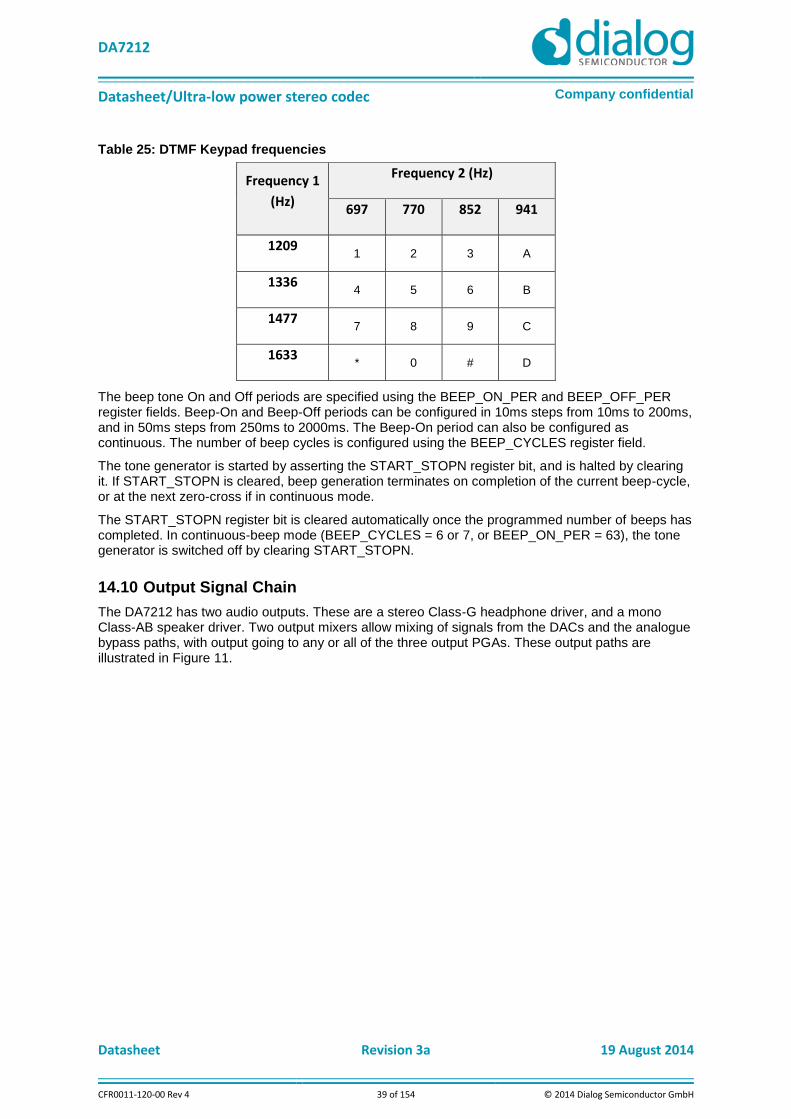
Table 25: DTMF Keypad frequencies ................................................................................................... 39
Table 26: Charge pump output voltage control .................................................................................. 42
Table 27: CP_THRESH_VDD2 Settings in DAC_VOL mode (CP_MCHANGE = 10) ................................ 43
Table 28: CP_THRESH_VDD2 Settings in Signal Size mode (CP_MCHANGE = 11) ............................... 43
Table 29: Charge pump current load control ...................................................................................... 46
Table 30: ADC/DAC Digital High Pass Filter specifications in Audio Mode ......................................... 47
Table 31: Wind noise high-pass filter specifications ........................................................................... 48
Table 32: DAC 5-Band Equaliser Turnover/Centre Frequencies ......................................................... 50
Table 33: Sample rate control register and corresponding system clock frequency .......................... 54

DA7212
Datasheet/Ultra-low power stereo codec Company confidential
Datasheet Revision 3a 19 August 2014
CFR0011-120-00 Rev 4 9 of 154 © 2014 Dialog Semiconductor GmbH
Table 34: PLL Input Divider .................................................................................................................. 55
Table 35: Example PLL configurations ................................................................................................. 56
Table 36: Ordering information ......................................................................................................... 141
Table 37: Audio inputs ....................................................................................................................... 143
Table 38: Microphone bias ................................................................................................................ 144
Table 39: Digital microphones ........................................................................................................... 144
Table 40: Headphone outputs ........................................................................................................... 145
Table 41: Speaker outputs ................................................................................................................. 145
Table 42: Headphone charge pump .................................................................................................. 146
Table 43: Digital interfaces – I2C ....................................................................................................... 147
Table 44: Offset calibration, MIC1_P and MIC2_P single ended, slave mode .................................. 149
Table 45: Digital interfaces - I2S ........................................................................................................ 150
Table 46: References ......................................................................................................................... 150
Table 47: Power supplies ................................................................................................................... 151
Table 48: Ground ............................................................................................................................... 151
1 Terms and definitions
ADC Analogue Digital Converter
ALC Automatic Level Control
DAC Digital Audio Converter
DAI Digital Audio Interface
DTMF Dual Tone Multi-Frequency
I2C Inter-Integrated Circuit interface
I2S Inter-IC Sound
PLL Phase Locked Loop
PSSR Power Supply Rejection Ratio
SNR Signal to Noise Ratio
TDM Time Division multiplexing
THD+N Total Harmonic Distortion plus Noise

DA7212
Datasheet/Ultra-low power stereo codec Company confidential
Datasheet Revision 3a 19 August 2014
CFR0011-120-00 Rev 4 10 of 154 © 2014 Dialog Semiconductor GmbH
2 Block diagram
MIC1_P/
DMICCLK
ADC_L
ADC
DIGITAL
FILTERS
Wind Noise
Filtering,
Automatic
Level Control
(ALC)
DAC
DIGITAL
FILTERS
Digital Mixer,
Digital
Volume,
5 Band
Equaliser,
Noise Gate
DAC_L
AUX_L
AUX_R
AUX
Input
SP_P
PLL
+ MIXIN_L
MIC2_P
+ MIXIN_R ADC_R
DAC_R
+
+
GND_CP
BC
LK
DA
TO
UT
WC
LK
DA
TIN
DIGITAL AUDIO
INTERFACE (DAI)
SP_NLINE_
AMP
Charge
Pump
HPCSP
HPCSN
1uF
1uF
VD
IG
VM
ID
GN
D_
A
Headphones
HP_L_
AMP
HP_R_
AMP
HP_L
HP_R
CONTROL
INTERFACE
SD
A
SC
L
1µF
HPCFN
HPCFP1uF
DA
CR
EF
BIAS
MIC_1
_AMP
MIC_2
_AMP
MIC1_N/
DMICIN
MICBIAS1
MICBIAS2
MIC2_N
MC
LK
GND_SENSE
VDD_SP
VR
EF
MIC
BIAS1
MIC
BIAS2
1µF
AUX_L
_AMP
AUX_R_
AMP
DA7212
VDD_MIC
BEEP
GENERATOR
+
VD
D_
IO
VD
D_
A
LDO
Figure 2: Block diagram showing component values for a typical application
ADC Digital Filter Analogue filter block incorporating wind noise filtering and Automatic Level Control (ALC)
DAC Digital Filter Digital filter block incorporating digital mixing, digital volume control, a 5-band equaliser and a noise gate
Beep Generator The Beep Generator block has two sine wave generators, each of which can be independently controlled. Output frequency is controllable in 10 Hz step sizes, and output gain is controllable in 3 dB steps from 0 dB to 45 dB. The Beep Generator block can also output standard DTMF keypad frequencies (see Table 25).

DA7212
Datasheet/Ultra-low power stereo codec Company confidential
Datasheet Revision 3a 19 August 2014
CFR0011-120-00 Rev 4 11 of 154 © 2014 Dialog Semiconductor GmbH
3 Pinout
HPCFP BCLK
HPCFN DATIN
WCLK SCL
DATOUT SDA
VDD_IO VDIG
AUX_L
AUX_R
MIC2_NHPCSN
GND_CPGND_
SENSE
HP_L HP_R
VDD_A VREF
DACREF VMID
GND_A SP_P
VDD_SP SP_N
VDD_MIC
MICBIAS1
MIC1_N
MIC2_P
HPCSP MICBIAS2
MIC1_P
1 2 3 4 5 6 8 9 10 11 12 13 14 15 16 17
A
B
C
D
7
1 2 3 4 5 6 8 9 10 11 12 13 14 15 16 177
Sensitive
Analogue
Noisy Digital
Low Power
(up to 100mA)
Medium Power
(up to 500mA)
Quiet Ground
Noisy Ground
View from above
“Live Bug”
KEY
MCLK
Figure 3: DA7212 Ball layout

DA7212
Datasheet/Ultra-low power stereo codec Company confidential
Datasheet Revision 3a 19 August 2014
CFR0011-120-00 Rev 4 12 of 154 © 2014 Dialog Semiconductor GmbH
Table 1: Pin descriptions
Pin Name Bump/Pin Function Alternate Function Class
Audio Inputs
MIC1_P C17 Differential mic. input 1 (pos) / Single-ended mic. input 1 (left)
Digital mic. clock (DMICCLK)
AI/DO
MIC1_N B16 Differential mic. input 1 (neg) / Single-ended mic. input 2 (left)
Digital Mic. data (DMICIN)
AI/DI
MIC2_P D16 Differential mic. input 2 (pos) / Single-ended mic. input 1 (right)
AI
MIC2_N C15 Differential mic. input 2 (neg) / Single-ended mic. input 2 (right)
AI
AUX_L C13 Single-ended auxiliary input left AI
AUX_R D14 Single-ended auxiliary input right AI
MICBIAS1 A15 Microphone bias output 1 AO
MICBIAS2 A17 Microphone bias output 2 AO
Audio Outputs
HP_L A3 True-ground headphone output left AO
HP_R A5 True-ground headphone output right AO
SP_P B12 Differential speaker output (pos) AO
SP_N A13 Differential speaker output (neg) AO
Audio Charge pump
HPCSP A1 Charge pump reservoir capacitor (pos) AIO
HPCSN C1 Charge pump reservoir capacitor (neg) AIO
HPCFP D2 Charge pump flyback capacitor (pos) AIO
HPCFN C3 Charge pump flyback capacitor (neg) AIO
Digital Interfaces
SDA C9 I2C bidirectional data DIO
SCL D8 I2C clock input DI
DATIN C5 DAI data input DIO
DATOUT C7 DAI data output DIO
BCLK D4 DAI bit clock DIO
WCLK D6 DAI word clock (L/R select) DIO
MCLK C11 Master clock DI
References
DACREF A7 Audio DAC reference capacitor AIO
VMID A9 Audio mid-rail reference capacitor AIO
GND_SENSE B4 Ground reference for headphone output AI
VREF B8 Bandgap reference capacitor AIO

DA7212
Datasheet/Ultra-low power stereo codec Company confidential
Datasheet Revision 3a 19 August 2014
CFR0011-120-00 Rev 4 13 of 154 © 2014 Dialog Semiconductor GmbH
Pin Name Bump/Pin Function Alternate Function Class
Supplies
VDD_A B6 Supply for analogue circuits PS
VDD_IO D10 Supply for digital interfaces PS
VDD_SP A11 Supply for speaker driver PS
VDD_MIC B14 Supply for microphone bias circuits PS
VDIG D12 Supply for digital circuits (LDO Output) PS
Grounds
GND_A B10 Analogue ground PG
GND_CP B2 Charge pump/digital ground PG
Table 2: Pin type definition
Pin type Description Pin type Description
DI Digital Input AI Analogue Input
DO Digital Output AO Analogue Output
DIO Digital Input/Output AIO Analogue Input/Output
DIOD Digital Input/Output open drain
PU Fixed pull-up resistor SPU Switchable pull-up resistor
PD Fixed pull-down resistor SPD Switchable pull-down resistor

DA7212
Datasheet/Ultra-low power stereo codec Company confidential
Datasheet Revision 3a 19 August 2014
CFR0011-120-00 Rev 4 14 of 154 © 2014 Dialog Semiconductor GmbH
4 Absolute maximum ratings
Table 3: Absolute maximum ratings
Symbol Parameter Test Conditions Min Typ Max Unit
Storage Temperature -65 +165 °C
Ta Operating Temperature
-40 +85 °C
VDD_SP
Supply Voltages
-0.3 6.0 V
VDD_A -0.3 2.75 V
VDD_IO
VDD_MIC -0.3 5.5 V
SDA
SCL
BCLK
WCLK
DATIN
DATOUT
Digital Interface Signals
-0.3 VDD_IO +
0.3
Package Thermal Resistance
60 °C/W
ESD Susceptibility Human body model 2 kV
Note 1 Stresses beyond those listed under ‘Absolute maximum ratings’ may cause permanent damage to the device. These are stress ratings only, so functional operation of the device at these or any other conditions beyond those indicated in the operational sections of the specification are not implied. Exposure to absolute maximum rating conditions for extended periods may affect device reliability.

DA7212
Datasheet/Ultra-low power stereo codec Company confidential
Datasheet Revision 3a 19 August 2014
CFR0011-120-00 Rev 4 15 of 154 © 2014 Dialog Semiconductor GmbH
5 Recommended operating conditions
Table 4: Recommended operating conditions
Symbol Parameter Test Conditions Min Typ Max Unit
Ta Operating temperature
-40 +85 °C
VDD_A Supply Voltages 1.6 2.65 V
VDD_IO 1.5 3.6 V
VDD_MIC 1.8 3.6 V
VDD_SP 0.95 5.25 V
Note 2 Within the specified limits, a life time of 10 years is guaranteed
Note 3 All Voltages are referenced to VSS unless otherwise stated
Note 4 Currents flowing into DA7212 are deemed positive. Currents flowing out are deemed negative
Note 5 All parameters are valid over the recommended temperature range and power supply range unless otherwise noted.

DA7212
Datasheet/Ultra-low power stereo codec Company confidential
Datasheet Revision 3a 19 August 2014
CFR0011-120-00 Rev 4 16 of 154 © 2014 Dialog Semiconductor GmbH
6 Electrical characteristics
Table 5: Power consumption
Operating Mode Conditions (Note 6) Power
Consumption Unit
Powerdown mode 5 µA
Digital playback to Lineout DAC_L/R to LINE, 10 kΩ load 2.2 mW
Digital playback to Headphone, no load
DAC_L/R to HP_L/R, quiescent 3.1 mW
Digital playback to Headphone, with load
DAC_L/R to HP_L/R, 16 Ω load, 0.1 mW at 0 dBFS
6.9 mW
Analogue bypass to Lineout AUX_L/R to LINE, 10 kΩ load 2.0 mW
Analogue bypass to Headphone, no load
AUX_L/R to HP_L/R, quiescent 2.6 mW
Analogue bypass to Headphone, with load
AUX_L/R to HP_L/R, 16 Ω load, 0.1 mW at 0 dBFS
6.7 mW
Microphone stereo record MIC_1/2 to ADC_L/R 2.1 mW
Microphone stereo record and digital playback to Headphone, no load
MIC_1/2 to ADC_L/R and DAC_L/R to HP_L/R, quiescent
4.8 mW
Microphone stereo record and digital playback to Headphone, with load
MIC_1/2 to ADC_L/R and DAC_L/R to HP_L/R, 16 Ω load,
0.1 mW at 0 dBFS 8.9 mW
Ultra-low power microphone mono record
MIC_1 to ADC_R, 8 kHz, quiescent, optimised clocking and bias
0.65 mW
Note 6 VDD_A=VDD_SP=VDD_IO=1.8 V, Ta=25°C, Fs=48 kHz, Charge pump signal-size mode, 0x95 = 0x06
Table 6: Reference voltage generation
Symbol Parameter Test Conditions Min Typ Max Unit
VMID Audio mid-rail voltage 0.45 × VDD_A V
CVMID VMID decoupling capacitor 1.0 µF
DACREF Audio DAC/ADC reference voltage 0.9 × VDD_A V
CDACREF DACREF decoupling capacitor 1.0 µF
VBG Bandgap voltage 1.2 V
CVBG Bandgap decoupling capacitor 1.0 µF

DA7212
Datasheet/Ultra-low power stereo codec Company confidential
Datasheet Revision 3a 19 August 2014
CFR0011-120-00 Rev 4 17 of 154 © 2014 Dialog Semiconductor GmbH
7 Parametric specifications
Table 7: Analogue to Digital Converter (ADC)
Symbol Parameter Test Conditions Min Typ Max Unit
VMAX Full-scale input signal
Digital output level = 0 dBFS
1.6 ×
VDD_A VPP
SNR
(Note 7)
Signal to Noise Ratio
A-weighted no input selected
90 dB
THD+N (Note 8) Total Harmonic Distortion plus Noise
-1 dBFS 44.1 kHz slave
mode -85 dB
-1 dBFS 32 kHz PLL mode
-80 dB
In-band Spurious Analog input level =
0 dBFS -85 dB
Channel separation 90 dB
BPASS Pass band 0.45*Fs Hz
BSTOP Stop band Fs 48 kHz
Fs = 88.2/96 kHz 0.56*Fs
7*Fs
3.5*Fs Hz
Pass band Ripple Voice mode
Music mode
±0.3
±0.1 dB
Stop band Attenuation
Voice mode
Music mode
70
55 dB
Group delay
Voice mode
Music mode
Fs = 88.2/96 kHz
4.3/Fs
18/Fs
9/Fs
600
µs
Group delay mismatch
Between left and right channels
2 µs
PSRR (Note 9)
with respect to VDD_A
Power Supply Rejection Ratio
20Hz – 2 kHz
20 kHz
70
50 dB
Note 7 SNR (Signal-to-Noise Ratio) is a ratio of the full-scale output signal level to the noise level with no signal applied
Note 8 THD+N (Total Harmonic Distortion plus Noise) is a ratio of the level of the harmonics and noise to the output signal
Note 9 PSRR (Power Supply Rejection Ratio) is a measure of the attenuation of a signal on the supply to the signal at the output

DA7212
Datasheet/Ultra-low power stereo codec Company confidential
Datasheet Revision 3a 19 August 2014
CFR0011-120-00 Rev 4 18 of 154 © 2014 Dialog Semiconductor GmbH
Table 8: Microphone bias
MICBIAS1 and MICBIAS2
Symbol Parameter Test Conditions Min Typ Max Unit
VMICBIAS Bias Voltage No load, VDD_MIC >
VMICBIAS + 200 mV
1.52 1.57 1.62
V 2.18 2.25 2.32
2.41 2.48 2.56
2.91 3.00 3.10
IBIAS Maximum Current Voltage drop < 50 mV 2 mA
PSRR with respect to VDD_MIC
Power Supply Rejection Ratio
20Hz – 200 Hz
>2 kHz
70
50 dB
VNOISE Output Noise Voltage VMICBIAS ≤ 2.2 V 5 µVRMS
Capacitive Load IBIAS < 100 µA
100 µA < IBIAS < 2 mA
100
200 pF

DA7212
Datasheet/Ultra-low power stereo codec Company confidential
Datasheet Revision 3a 19 August 2014
CFR0011-120-00 Rev 4 19 of 154 © 2014 Dialog Semiconductor GmbH
Table 9: Input mixing units
(MIC1_P/MIC1_N/MIC2_P/MIC2_N/AUX_L/AUX_R ) to ADC_L/ADC_R
Symbol Parameter Test Conditions Min Typ Max Unit
VMAX Full-scale input signal
Single-ended
Differential
MIC_1/2_AMP = AUX_L/R_AMP = MIXIN_L/R =
0dB
0.8 × VDD_A
1.6 × VDD_A VPP
RIN Input resistance MIC, single-ended
AUX
12
6
15
18
40 kΩ
CIN Input capacitance 1 pF
Amplitude ripple 20Hz to 20 kHz -0.5 +0.5 dB
Programmable gain
MIC_1_AMP and MIC_2_AMP
AUX_L_AMP and AUX_R_AMP
MIXIN_L and MIXIN_R
-6
-54
-4.5
36
15
18
dB
Programmable gain step size
MIC_1_AMP and MIC_2_AMP
AUX_L_AMP and AUX_R_AMP
MIXIN_L and MIXIN_R
6
1.5
1.5
dB
Absolute gain accuracy
0 dB @ 1 kHz -1.0 +1.0 dB
Left/Right gain mismatch
20 Hz to 20 kHz -0.1 +0.1 dB
Gain step error 20 Hz to 20 kHz -0.1 +0.1 dB
Input noise level
Inputs connected to GND, A-weighted, input-referred, measured @ ADC output
MIC_1/2_AMP = 24 dB
AUX_L/R_AMP = 15 dB
5
6.5
µVRMS
PSRR with respect to VDD_A
Power supply rejection ratio
Single-ended input
20Hz to 2 kHz
20 kHz
70
50
dB
Differential input
20Hz to 2 kHz
20 kHz
90
70
dB

DA7212
Datasheet/Ultra-low power stereo codec Company confidential
Datasheet Revision 3a 19 August 2014
CFR0011-120-00 Rev 4 20 of 154 © 2014 Dialog Semiconductor GmbH
8 Digital signal processing
Table 10: ADC/DAC Digital high-pass filter cut-off frequencies in music mode
Sampling Frequency (kHz)
Music Mode – Cut-Off Frequency (-3 dB) in Hz at
ADC_AUDIO_HPF_CORNER / DAC_AUDIO_HPF_CORNER Register Settings
00 01 10 11
8 0.3 0.7 1.3 2.7
11.025 0.4 0.9 1.8 3.7
12 0.5 1 2 4
16 0.7 1.3 2.7 5.3
24 1 2 4 8
32 1.3 2.7 5.3 10.7
44.1 1.8 3.7 7.3 14.7
48 2 4 8 16
88.2 3.6 7.4 14.6 29.4
96 4 8 16 32
Table 11: ADC/DAC Digital high-pass filter cut-off frequencies in voice mode
Sampling
Frequency (kHz)
Voice Mode – Cut-Off Frequency (-3 dB) in Hz at
ADC_VOICE_HPF_CORNER / DAC_VOICE_HPF_CORNER Register Settings
000 001 010 011 100 101 110 111
8 2.66 25 50 100 150 200 300 400
11.025 3.5 35 69 138 207 275 415 553
12 4 37.5 75 150 225 300 450 600
16 5 50 100 200 300 400 600 800

DA7212
Datasheet/Ultra-low power stereo codec Company confidential
Datasheet Revision 3a 19 August 2014
CFR0011-120-00 Rev 4 21 of 154 © 2014 Dialog Semiconductor GmbH
Table 12: DAC 5-Band equaliser frequencies
Sampling
Frequency (kHz)
Centre/Cutoff frequency of 5-Band Equaliser (Hz)
Band 1
Cutoff (Note 10)
Band 2
Centre
Band 3
Centre
Band 4
Centre
Band 5
Cutoff (Note 10)
8 21 85 563 1151 2909
11.025 29 117 776 2137 4009
12 31 128 845 2326 4364
16 41 90 441 2128 5840
22.05 56 124 607 2933 8048
24 61 135 664 3192 8759
32 58 95 418 1731 6374
44.1 80 132 577 2385 8784
48 87 143 628 2596 9560
88.2 N/A N/A N/A N/A N/A
96 N/A N/A N/A N/A N/A
Note 10 For equaliser bands 1 and 5 the cut-off frequency depends on the gain setting. The figures quoted in this table refer to the –1 dB point with the band gain set to –3 dB

DA7212
Datasheet/Ultra-low power stereo codec Company confidential
Datasheet Revision 3a 19 August 2014
CFR0011-120-00 Rev 4 22 of 154 © 2014 Dialog Semiconductor GmbH
Table 13: Beep generator
Symbol Parameter Test Conditions Min Typ Max Unit
Single-tone frequency 10 12000 Hz
Single-tone frequency step 10 Hz
Dual-tone modulation frequency A
697 770 852 941
Hz
Dual-tone modulation frequency B
1209 1336 1477 1633
Hz
Output signal level -45 0 dBFS
Output signal step size 3 dB
TON,TOFF On/off pulse duration 10 2000 ms
On/off pulse step size TON/OFF=10 – 200ms
TON/OFF=200 – 2000ms
10
50 ms
On/off pulse repeat
continuous mode
1,2,4,8,16,32
∞ cycles

DA7212
Datasheet/Ultra-low power stereo codec Company confidential
Datasheet Revision 3a 19 August 2014
CFR0011-120-00 Rev 4 23 of 154 © 2014 Dialog Semiconductor GmbH
9 Audio outputs
Table 14: Digital to Analogue Converter (DAC)
Symbol Parameter Test Conditions Min Typ Max Unit
VMAX Full-scale output signal Digital input level =
0 dBFS 1.6×VDD_A VPP
SNR Signal to Noise Ratio A-weighted 100 dB
THD+N Total Harmonic Distortion Plus Noise
-1 dBFS 44.1 kHz slave
mode -90 dB
-1 dBFS 32 kHz PLL mode
-80 dB
Channel separation 90 dB
BPASS Pass band 0.45×Fs kHz
BSTOP Stop band Fs 48 kHz
Fs = 88.2/96 kHz 0.56×Fs
7×Fs
3.5×Fs kHz
Pass band Ripple Voice mode
Music mode
±0.15
±0.1 dB
Stop band Attenuation Voice mode
Music mode
70
55 dB
Group delay
Voice mode
Music mode
Fs = 88.2/96 kHz
4.8/Fs
18.5/Fs
9/Fs
650
µs
Group delay variation 20Hz to 20 kHz 1 µs
Group delay mismatch Between left and
right channels 2 µs
PSRR with respect to VDD_A
Power Supply Rejection Ratio
20Hz to 2 kHz
20 kHz
70
50 dB

DA7212
Datasheet/Ultra-low power stereo codec Company confidential
Datasheet Revision 3a 19 August 2014
CFR0011-120-00 Rev 4 24 of 154 © 2014 Dialog Semiconductor GmbH
Table 15: Class AB lineout amplifier / speaker
From DAC_L/DAC_R to (SP_P, SP_N)
Symbol Parameter Test Conditions Min Typ Max Unit
VMAX Full-scale output signal No load 1.8×VDD_SP
VPP
PMAX Maximum output power
VDD_SP = 1.2 V THD < 10 %
RLOAD = 8 Ω, 1 kHz 65 mWRMS
VDD_SP = 1.5 V THD < 10 %
RLOAD = 8 Ω, 1 kHz 115 mWRMS
VDD_SP = 3.7 V THD < 10 %
RLOAD = 8 Ω, 1 kHz 745 mWRMS
VDD_SP = 5.0 V
THD < 10 % RLOAD = 8 Ω, 1 kHz
1200 mWRMS
RLOAD Load impedance
6.4
8
1
200
Ω
µH
pF
Frequency response ±0.5 dB 20 20k Hz
Amplitude ripple 20Hz to 20 kHz -0.5 0.5 dB
Programmable gain -48 +15 dB
Mute attenuation 100 dB
Programmable gain step size
1 dB
Absolute gain accuracy 0 dB @ 1 kHz -0.8 +0.8 dB
Gain step error 20 Hz to 20 kHz -0.1 +0.1 dB
SNR Signal to noise ratio A-weighted gain = 0 dB
VDD_SP = 1.6 V 96.5 dB
VNOISE Output Noise Level Non A-weighted Gain ≤ -15 dB
20Hz to 20 kHz 6 µV
THD+N Total Harmonic Distortion Plus Noise
VDD_SP = 1.6 V -1 dBFS
44.1 kHz slave mode RLOAD > 2 kΩ
-86 dB
VDD_SP = 1.6 V -1 dBFS
32 kHz PLL mode RLOAD > 2 kΩ
-80 dB
PSRR with
respect to VDD_SP
Power Supply Rejection Ratio
20 Hz to 2 kHz
20 kHz
90
70 dB

DA7212
Datasheet/Ultra-low power stereo codec Company confidential
Datasheet Revision 3a 19 August 2014
CFR0011-120-00 Rev 4 25 of 154 © 2014 Dialog Semiconductor GmbH
Table 16: True Ground charge pump
HPCSP and HPCSN
Symbol Parameter Test Conditions Min Typ Max Unit
VDDCSP Positive rail output CP_MOD = 11
CP_MOD = 10
VDD_A
VDD_A / 2 V
VDDCSN Negative rail output CP_MOD = 11
CP_MOD = 10
-VDD_A -(VDD_A /
2) V
Flyback capacitor One capacitor 1.0 µF
Reservoir capacitors Two capacitors 1.0 µF

DA7212
Datasheet/Ultra-low power stereo codec Company confidential
Datasheet Revision 3a 19 August 2014
CFR0011-120-00 Rev 4 26 of 154 © 2014 Dialog Semiconductor GmbH
Table 17: True Ground headphone amplifier
From DAC_L/DAC_R to (HP_L/HP_R)
Symbol Parameter Test Conditions Min Typ Max Unit
VMAX Full-scale Output Signal No load 1.6×VDD_A VPP
DC output offset HP Gain < -30 dB 100 µV
PMAX Maximum power per channel
VDD_A = 1.6 V THD < 0.1 %
RLOAD=16 Ω, 1 kHz
L = 23
R = 23 mWRMS
VDD_A = 1.8 V THD < 0.1 %
RLOAD=16 Ω, 1 kHz
L = 29
R = 29 mWRMS
VDD_A = 2.5 V THD < 0.1 %
RLOAD=16 Ω, 1 kHz
L = 67
R = 67 mWRMS
RLOAD
LLOAD
CLOAD
Load Impedance
13
16
400
500
Ω
µH
pF
Frequency Response ±0.5 dB 20 20k Hz
Amplitude Ripple 20Hz to 20 kHz -0.5 +0.5 dB
Programmable Gain -56 +6 dB
Mute Attenuation 70 dB
Programmable Gain Step Size
1.0 dB
Absolute Gain Accuracy 0 dB @ 1 kHz -0.8 +0.8 dB
Input Gain L/R-Mismatch 20Hz to 20 kHz -0.1 +0.1 dB
Input Gain Step Error 20Hz to 20 kHz -0.1 +0.1 dB
SNR Signal to Noise Ratio
A-weighted gain = 0 dB
VDD_A = 2.5 V
VDD_A = 1.8 V
100
98
dB
VNOISE Output Noise Level 20 to 20 kHz,
non A-weighted gain < -20 dB
2.5 µVrms
THD+N Total Harmonic Distortion Plus Noise
VDD_A = 1.6 V -5 dBFS
RLOAD=16 Ω -87 dB
PSRR with
respect to VDD_A
Power Supply Rejection Ratio
20Hz to 2 kHz
20 kHz
70
50 dB

DA7212
Datasheet/Ultra-low power stereo codec Company confidential
Datasheet Revision 3a 19 August 2014
CFR0011-120-00 Rev 4 27 of 154 © 2014 Dialog Semiconductor GmbH
11 Clock generation
Table 18: MCLK Input
Symbol Parameter Test Conditions Min Typ Max Unit
Input Amplitude MCLK squarer enabled
MCLK squarer disabled
0.3
0.9×VDD_IO
VDD_IO
VDD_IO V
Input Impedance DC impedance > 10 MΩ 300
0.5
1
2
Ω
pF
12 Phase Locked Loop (PLL)
Table 19: PLL Mode
Symbol Parameter Test Conditions Min Typ Max Unit
JC
JA MCLK Input Jitter Cycle jitter (rms)
Absolute jitter (rms)
50
100
ps
ps
FIN Input frequency Normal mode
32 kHz mode
2 (Note 11)
5 - 50
32.768
50
MHz
kHz
SRM Tracking Range DAI slave mode WCLK frequency
variation -4 4 %
SRM Tracking Rate DAI slave mode WCLK drift rate
50 ppm/s
Note 11 See section 32 kHz PLL Mode (DAI Master) on page 56 for further details on using an MCLK frequency between 2 MHz and 5 MHz

DA7212
Datasheet/Ultra-low power stereo codec Company confidential
Datasheet Revision 3a 19 August 2014
CFR0011-120-00 Rev 4 28 of 154 © 2014 Dialog Semiconductor GmbH
Table 20: Bypass Mode
Symbol Parameter Test Conditions Min Typ Max Unit
JC
JA Input Jitter
Cycle jitter (rms)
Absolute jitter (rms)
TBD
TBD
ps
ps
FIN Input frequency
Sample frequency:
11.025, 22.05, 44.1, 88.2 kHz
8, 12, 16, 24, 32, 48, 96 kHz
11.2896
12.288
MHz
13 Digital interfaces
Table 21: I/O Characteristics
Symbol Parameter Test
Conditions Min Typ Max Unit
VIH SCL, SDA, Input High Voltage
0.7*VDD_IO V
VIL SCL, SDA, Input Low Voltage
0.3*VDD_IO V
VIH MCLK, BCLK, WCLK, DATIN, DATOUT Input High Voltage
0.7*VDD_IO V
VIL MCLK, BCLK, WCLK, DATIN, DATOUT Input Low Voltage
0.3*VDD_IO V
VOL @3mA
SDA Output Low Voltage 0.24 V

DA7212
Datasheet/Ultra-low power stereo codec Company confidential
Datasheet Revision 3a 19 August 2014
CFR0011-120-00 Rev 4 29 of 154 © 2014 Dialog Semiconductor GmbH
SCL
SDA
STH
CLKL CLKH
DST TSSDHT
Figure 4: I2C Bus Timing
Table 22: I2C Control bus
Symbol Parameter Test Conditions
(Note 12) Min Typ Max Unit
Bus free time STOP to START 500 ns
Bus line capacitive load 150 pF
Standard/Fast Mode
SCL clock frequency 0 1000 kHz
Start condition setup time 260 ns
STH Start condition hold time 260 ns
CLKL SCL low time 500 ns
CLKH SCL high time 260 ns
SCL rise/fall time Input requirement 1000 ns
SDA rise/fall time Input requirement 300 ns
DST SDA setup time 50 ns
DHT SDA hold time 0 ns
TSS Stop condition setup time 260 ns
High-Speed Mode
SCL clock frequency 0 3400 kHz
Start condition setup time 160 ns
STH Start condition hold time 160 ns
CLKL SCL low time 160 ns
CLKH SCL high time 60 ns
SCL rise/fall time Input requirement 160 ns

DA7212
Datasheet/Ultra-low power stereo codec Company confidential
Datasheet Revision 3a 19 August 2014
CFR0011-120-00 Rev 4 30 of 154 © 2014 Dialog Semiconductor GmbH
SDA rise/fall time Input requirement 160 ns
DST SDA setup time 10 ns
DHT SDA hold time 0 ns
TSS Stop condition setup time 160 ns
Note 12 VDD_IO = 1.8 V
T
tlCthC
BCLK
DATIN
tf
tsD
DATOUT
WCLK
tr
tdCW
tdCDtdWD
thD
tsW thW
Figure 5 Digital audio interface timing diagram
Note 13 Diagram shown is valid for all modes except DSP. For DSP mode the BCLK signal is inverted
Table 23: Digital Audio Interface Timing (I2S/DSP in Master/Slave Mode)
Symbol Parameter Test
Conditions (Note 14)
Min Typ Max Unit
Input impedance DC impedance
> 10MΩ
300
1.0
2.5
Ω
pF
T BCLK period 75 ns
tr BCLK rise time 8 ns
tf BLCK fall time 8 ns
thC BCLK high period 40 % 60 % T
tlC BCLK low period 40 % 60 % T
tdCW BCLK to WCLK delay
-30 % +30 % T
tdCD BCLK to DATOUT delay
-30 % +30 % T
thW WCLK high time DSP mode 100 % T

DA7212
Datasheet/Ultra-low power stereo codec Company confidential
Datasheet Revision 3a 19 August 2014
CFR0011-120-00 Rev 4 31 of 154 © 2014 Dialog Semiconductor GmbH
Non-DSP
mode
Word length
(Note 15) T
tlW
WCLK low time
DSP mode 100 % T
Non-DSP
mode
Word length
(Note 16) T
tsW WCLK setup time Slave mode 7 ns
thW WCLK hold time Slave mode 2 ns
tsD DATIN setup time 7 ns
thD DATIN hold time 2 ns
tdWD DATOUT to WCLK delay
DATOUT is synchronised to BCLK
Note 14 VDD_IO = 1.8 V
Note 15 WCLK must be high for at least the word length number of BCLK periods
Note 16 WCLK must be low for at least the word length number of BCLK periods
Codec Start-Up Time 13.1
After the audio system controller has been enabled using SYSTEM_MODES_INPUT and SYSTEM_MODES_OUTPUT, the startup times for the various codec paths are as specified below:
Table 24 Codec start-up times
Source Output Comment Min Typ Max Unit
VMID VMID > 90 % of final
value 1µF capacitor
25 ms
Any analogue input or DAC_L/R
HP_L HP_R
PLL bypass or PLL normal mode
200 200 ms
Any analogue input or DAC_L/R
HP_L HP_R
PLL SRM or PLL 32 kHz mode
500 ms
Any analogue input or DAC_L/R
SP_P SP_N
PLL bypass or PLL normal mode
250 ms
Any analogue input ADC_L ADC_R
PLL bypass or PLL normal mode
200 ms
Any analogue input ADC_L ADC_R
PLL SRM or PLL 32 kHz mode
600 ms

DA7212
Datasheet/Ultra-low power stereo codec Company confidential
Datasheet Revision 3a 19 August 2014
CFR0011-120-00 Rev 4 32 of 154 © 2014 Dialog Semiconductor GmbH
14 Functional description
General description 14.1
DA7212 is an ultra-low-power audio CODEC with true ground headphone drivers, mixing capability, and digital audio enhancement. It offers HiFi audio quality with class-leading power consumption for portable media and embedded applications.
Featuring a high efficiency headphone amplifier and minimum supply voltage of 1.6 V, the ultra-low 3.1 mW quiescent power consumption extends music playback time for battery-operated equipment.
Control and data interfaces are supplied from a dedicated VDD_IO rail. For compatibility with higher I/O levels, an extended voltage range up to 3.6 V can be selected.
The integrated PLL uses a fractional-N architecture that supports frequencies from 2 MHz to 50 MHz. Standard mobile phone/USB system clock frequencies are supported, and audio data synchronisation is supported even when no master clock is available.
The DA7212 has a stereo pair of single-ended line inputs as well as two microphone inputs, each of which can be configured as single-ended or differential. Both line and microphone signals can be routed to the ADC or directly to the output mixers via a bypass path. In addition, the DA7212 supports both single and dual-channel digital microphone inputs by routing the digital signals directly to the ADC digital filters.
Input and output mixers with stereo-to-mono conversion also support mono configurations such as single speaker outputs.
Three output drivers are available in the output stage of the DA7212. A stereo true-ground amplifier directly drives standard 3-wire 16 ohm headphones while a differential mono speaker amplifer is capable of driving 1.2W into 8 ohms.
Audio enhancement functions are performed digitally including programmable high-pass filtering, 5-band EQ, noise-gate and an AGC with configurable attack and decay parameters.
The multislot I2S/PCM Digital Audio Interface (DAI) supports all common sample rates between 8 kHz and 96 kHz in master or slave modes.
The CODEC register space can be accessed via the I2C interface of DA7212 on the default 7-bit address 0x1A.
DA7212 implements a unique Smart Controller that enables easy configuration of the Codec for different application scenarios, thereby reducing the number of register writes needed for each case. The Smart Controller runs automatically once enabled, and is optimised to allow pop-free and click-free power-up and power-down operation.
Input Signal Chain 14.2
The DA7212 has a stereo pair of single-ended line inputs as well as two microphone inputs that can each be configured as single-ended or differential. Both line and microphone signals can be routed to the ADC or directly to the output mixers via a bypass path. In addition, the DA7212 supports both single and dual channel digital microphone inputs by routing the digital signals directly to the ADC digital filters. The input routing paths and input amplifier gain ranges are illustrated in Figure 5.

DA7212
Datasheet/Ultra-low power stereo codec Company confidential
Datasheet Revision 3a 19 August 2014
CFR0011-120-00 Rev 4 33 of 154 © 2014 Dialog Semiconductor GmbH
MIC_2_AMP-6dB to +36dB
in 6dB steps
AUX_L_AMP
MIXIN_L
-4.5dB to +18dB
in 1.5dB steps
AUX_L
MIC2_N
MICBIAS1
MIC2_P
AUX_R
MICBIAS2
MIC_1_AMP
AUX_R_AMP
-54dB to +15dB
in 1.5dB steps
MIXIN_R
to ADC_L
to ADC_R
MIC1_N /
DMICIN
MIC1_P /
DMICCLK
from PLL
to ADC filters
-6dB to +36dB
in 6dB steps
-54dB to +15dB
in 1.5dB steps
-4.5dB to +18dB
in 1.5dB steps
Figure 6: Audio input routing and gain ranges
Microphone Inputs 14.3
The DA7212 includes two pairs of analogue microphone inputs that can be connected in three ways:
fully differential mode for improved common mode noise rejection
single ended or pseudo-differential mode by connecting MIC1_N or MIC2_N to GND (see Figure 7). The microphone source is specified using MIC_1_AMP_IN_SEL and MIC_2_AMP_IN_SEL
single ended or pseudo-differential mode by connecting MIC1_P or MIC2_P to GND (see Figure 7). The microphone source is specified using MIC_1_AMP_IN_SEL and MIC_2_AMP_IN_SEL
The microphone PGAs are enabled by the MIC_1_AMP_EN / MIC_2_AMP_EN controls and can be muted via MIC_1_AMP_MUTE_EN / MIC_2_AMP_MUTE_EN. For maximum flexibility, each microphone channel includes an individual gain setting (MIC_1_AMP_GAIN / MIC_2_AMP_GAIN controls) that has a range of -6 dB to +36 dB in 6 dB steps. The currently active gain setting of each microphone is stored in MIC_1_GAIN_STATUS and MIC_2_GAIN_STATUS.
A maximum analogue gain from microphone to ADC input of +54 dB with a resolution of 1.5 dB can be selected.

DA7212
Datasheet/Ultra-low power stereo codec Company confidential
Datasheet Revision 3a 19 August 2014
CFR0011-120-00 Rev 4 34 of 154 © 2014 Dialog Semiconductor GmbH
MICBIAS2
MIC1_N
(c) Single-ended
MICBIAS1
MIC1_P
(c) Single-ended
MICBIAS1
MIC1_P
MIC1_N
(b) Pseudo-differential
MICBIAS1
MIC1_P
MIC1_N
(a) Differential
Figure 7: Typical microphone application for MIC1 (MIC2 is similar)
Standard electret microphones can be supplied from an embedded microphone bias regulator, enabled using the MICBIAS2_EN control bit. Two separate outputs are available on either the MICBIAS1 pin or the MICBIAS2 pin. These are enabled using the MICBIAS2_EN and MICBIAS1_EN controls. The voltage on the MICBIAS pins is set to 1.6 V, 2.2 V, 2.5 V or 3.0 V by the MICBIAS2_LEVEL and MICBIAS1_LEVEL controls. The microphone bias generates an ultra-low-noise voltage to feed several electret microphones with up to 2mA.
Digital microphones 14.4
DA7212 implements a digital microphone interface via a clock output (shared pin with MIC1_P) and a serial data input (shared pin with MIC1_N). The serial data is a sigma delta sampled bitstream. Modulators up to 3rd Order are supported.
MICBIAS1 can be used to power the digital microphone, but it must be enabled because it is MICBIAS1 that supplies the digital microphone pins.
The clock and data pins are shared with two analogue microphone inputs. This allows DA7212 to record from single or dual channel digital microphones, or from conventional mono/stereo analogue microphones.
The clock frequency can be selected to be either 1.5 MHz or 3 MHz by using DMIC_CLK_RATE control.
Single channel and dual channel digital microphone modules are supported. The dual channel modules change the output data on both the rising and the falling edges of the clock, as illustrated in Figure 7. In this case DMIC_SAMPLEPHASE must be set to zero in order to enable the sample detection at the edges of the clock. Each DMIC input is enabled via DMIC_L_EN / DMIC_R_EN and is associated with a clock edge via DMIC_DATA_SEL control.
A digital microphone requires a decimation filter to reconstruct the signal at the required sampling rate. The ADC decimation filters are re-used for this purpose, so either digital microphones or analogue sources may be used for recording at any one time.

DA7212
Datasheet/Ultra-low power stereo codec Company confidential
Datasheet Revision 3a 19 August 2014
CFR0011-120-00 Rev 4 35 of 154 © 2014 Dialog Semiconductor GmbH
DMICCLK
Output 1 to DMIC1
Output 2 to DMIC1
DATAVALID
Falling edge to valid data on 1
Falling edge to high impedance on 2
Rising edge to valid data on 2
Rising edge to high impedance on 1
DATAVALID
DATAHIGH Z
DATAVALID
DATAHIGH Z
DATAHIGH Z
Figure 8: Digital microphone timing example
Auxiliary inputs 14.5
Standard analogue sources (for example FM radio) are supported via the AUX stereo line inputs. Auxiliary inputs are enabled by AUX_L_AMP_EN / AUX_R_AMP_EN. They can be summed with each other, and with the microphone paths, which enables flexible audio mixing.
Each channel includes individual gain settings in 1.5 dB steps from -54 dB to +15 dB using AUX_L_AMP_GAIN and AUX_R_AMP_GAIN. The auxiliary amplifiers can be muted by asserting AUX_L_AMP_MUTE_EN and AUX_R_AMP_MUTE_EN.
Changes in gain can be synchronised with zero-crossing by asserting the AUX_L_AMP_ZC_EN and AUX_R_AMP_ZC_EN bits. If no zero-crossing is detected within approximately 85ms, the gain change is applied unconditionally. The sensitivity of the zero-cross detector is maximised by automatic selection of whether the zero-cross detection is performed at the input to the AUX amplifier, or the output from it. This is configured using the AUX_L_AMP_ZC_SEL and AUX_R_AMP_ZC_SEL controls.
Smooth changes in gain are enabled by asserting the AUX_L_AMP_RAMP_EN and AUX_R_AMP_RAMP_EN controls. If the ramp controls are asserted, the rate of ramping is specified by the GAIN_RAMP_RATE control. Any zero-cross activation is over-ridden if gain ramping is set.
The currently active AUX_L_GAIN and AUX_R_GAIN settings are stored in the AUX_L_GAIN_STATUS and AUX_R_GAIN_STATUS controls.
NOTE: When implementing fade-in and fade-out effects on the record path, it is recommended that this is done through ADC L and ADC_R. When implementing fade-in and fade-out effects on the output path, this should be done using the HP L, HP R and LINE amplifiers.
Input mixers 14.6
The DA7212 has two second level input amplifiers (MIXIN_L and MIXIN_R) that mix the analogue inputs as well as providing up to 18 dB extra gain. They are enabled by asserting the controls MIXIN_L_AMP_EN and MIXIN_R_AMP_EN. Gain can be controlled in 1.5 dB steps from 4.5 dB to +18 dB using the MIXIN_L_GAIN and MIXIN_R_GAIN register bits.
Zero-crossing can be enabled by asserting MIXIN_L_AMP_ZC_EN or MIXIN_R_AMP_ZC_EN. If no zero crossing is detected within approximately 85ms, the gain change is applied unconditionally. Smooth changes in gain are performed by asserting the MIXIN_L_AMP_RAMP_EN and MIXIN_R_AMP_RAMP_EN controls. If the ramp controls are asserted, the rate of ramping is specified by the GAIN_RAMP_RATE control. Any zero-cross activation is over-ridden if gain ramping is set.

DA7212
Datasheet/Ultra-low power stereo codec Company confidential
Datasheet Revision 3a 19 August 2014
CFR0011-120-00 Rev 4 36 of 154 © 2014 Dialog Semiconductor GmbH
The left mixer accepts inputs from AUX_L_AMP and from either or both of the microphone PGAs (MIC_1_AMP and MIC_2_AMP), as well as from the right mixer MIXIN_R for stereo-to-mono conversion. Similarly the right mxer accepts inputs from AUX_R_AMP and from either or both of the microphone PGAs (MIC_1_AMP and MIC_2_AMP), as well as from the left mixer MIXIN_L for stereo-to-mono conversion. Input channel selection is determined by MIXIN_L_MIX_SELECT and MIXIN_R_MIX_SELECT.
The mixers can be muted using the MIXIN_L_AMP_MUTE_EN and MIXIN_R_AMP_MUTE_EN controls. The currently active gain settings are stored in MIXIN_L_AMP_GAIN_STATUS and MIXIN_R_AMP_GAIN_STATUS registers.
Stereo audio ADC 14.7
DA7212 includes a low power 24-bit high quality stereo audio ADC that supports sampling rates from 8 kHz to 96 kHz. The sample rate is specified using the SR register.
The stereo ADC can be enabled and disabled on either channel using ADC_L_EN and ADC_R_EN, thereby providing the opportunity to save power during mono operation.
The ADC channels offer a configurable digital gain from 83.25 dB to +12 dB in 0.75 dB steps after the digital conversion. Individual gain settings can be programmed via controls ADC_L_DIGITAL_GAIN and ADC_R_DIGITAL_GAIN. The currently active gain settings are stored in ADC_L_GAIN_STATUS and ADC_R_GAIN_STATUS registers.
Muting, and the ramping of digital gain changes, can be controlled using the dedicated ADC_L_CTRL and ADC_R_CTRL registers. If the ramping is enabled using the control bits ADC_L_RAMP_EN and ADC_R_RAMP EN, the rate of the ramping is controlled using GAIN_RAMP_RATE.
To enable saturation-free signals with maximum signal to noise ratios, the input levels of the ADC are adjusted with second level PGAs that are enabled with controls MIXIN_L_AMP_EN and MIXIN_R_AMP_EN. The signal routing and mix are configured using the MIXIN_L_SELECT and MIXIN_R_SELECT registers.
On the dedicated MIXIN_L_CTRL and MIXIN_R_CTRL registers, settings such as gain changes at zero-cross (for smooth volume changes), ramping of gain changes at signal zero cross ramping of gain changes, and mute can be configured. If the ramping is enabled using the control bits MIXIN_L_AMP_RAMP_EN and MIXIN_R_AMP_RAMP_EN, the speed of the ramp can be configured on GAIN_RAMP_RATE.
Automatic Level Control (ALC) 14.8
For improved sound recordings of signals with a large volume range, the DA7212 offers a fully-configurable automatic recording level control (ALC) for microphone inputs. This is enabled via the ALC_L_EN and ALC_R_EN controls, and can be enabled independently on either left or right channel. It is recommended that the ALC is only enabled in stereo as this applies the same gain to both channels and so protects the pan of stereo signals.
The ALC monitors the digital signal after the ADC and adjusts the microphones’ analogue and digital gain to maintain a constant recording level, whatever the analogue input signal level.
Operation of ALC is illustrated in Figure 9. When the input signal volume is high, the ALC system will reduce the overall gain until the output volume is below the specified maximum value. When the input signal volume is low, the ALC will increase the gain until the output volume increases above the specified minimum value. If the output signal is within the desired signal level (between the specified minimum and maximum levels), the ALC does nothing.
The maximum and the minimum thresholds that trigger a gain change of the ALC are programmed by the ALC_THRESHOLD_MAX and ALC_THRESHOLD_MIN controls.

DA7212
Datasheet/Ultra-low power stereo codec Company confidential
Datasheet Revision 3a 19 August 2014
CFR0011-120-00 Rev 4 37 of 154 © 2014 Dialog Semiconductor GmbH
ALC Input
ALC Gain
ALC Output
AL
C M
AX
leve
l
AL
C M
IN
leve
l
Release time Attack time
Figure 9: Principle of Operation of the ALC
The total gain is made up of an analogue gain, which is applied to the microphone PGAs, and a digital gain, which is implemented in the filtering stage. The ALC block monitors and controls the gain of the microphone PGAs and the ADC. Note that although the ALC is controlling the gain, it does not modify any of the registers MIC_1_AMP_GAIN, MIC_2_AMP_GAIN, ADC_L_DIGITAL_GAIN and ADC_R_DIGITAL_GAIN. These registers are ignored while the ALC is in operation.
The minimum and maximum levels of digital gain that can be applied by the ALC are controlled using ALC_ATTEN_MAX and ALC_GAIN_MAX.
Similarly the minimum and maximum levels of analogue gain are controlled by ALC_ANA_GAIN_MIN and ALC_ANA_GAIN_MAX.The rates at which the gain is changed are defined by the attack and decay rates in register ALC_CTRL2. When attacking, the gain decreases with ALC_ATTACK rate. When decaying, the gain increases with ALC_RELEASE rate.
The hold-time is defined by ALC_HOLD in the ALC_CTRL3 register. This controls the length of time that the system maintains the current gain level before starting to decay. This prevents unwanted changes in the recording level when there is a short-lived ‘spike’ in input volume, for example when recording speech.
Typically the attack rate should be much faster than the decay rate, as it is necessary to reduce rapidly increasing waveforms as quickly as possible, whereas fast release times will result in the signal appearing to ‘pump’. The ALC also has an anti-clipping function that applies a very fast attack rate when the input signal is close to full-range. This prevents clipping of the signal by reducing the signal gain at a faster rate than would normally be applied. The anti-clip function is enabled using ALC_ANTICLIP_EN, and the threshold above which it is activated is set in the range 1/128 full-scale to full-scale using ALC_ANTICLIP_LEVEL.
A recording Noise-Gate feature is provided to avoid increasing the gain of the channel when there is no signal, or when only a noise signal is present. Boosting a signal on which only noise is present is known as ‘noise pumping’. The Noise-Gate prevents this. Whenever the level of the input signal drops below the noise threshold configured in ALC_NOISE, the channel gain remains constant.
DA7212
Datasheet/Ultra-low power stereo codec Company confidential
Datasheet Revision 3a 19 August 2014
CFR0011-120-00 Rev 4 38 of 154 © 2014 Dialog Semiconductor GmbH
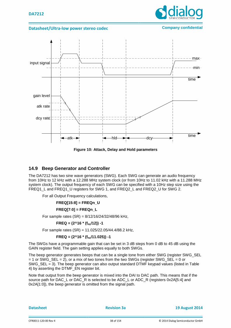
Figure 10: Attack, Delay and Hold parameters
Beep Generator and Controller 14.9
The DA7212 has two sine wave generators (SWG). Each SWG can generate an audio frequency from 10Hz to 12 kHz with a 12.288 MHz system clock (or from 10Hz to 11.02 kHz with a 11.288 MHz system clock). The output frequency of each SWG can be specified with a 10Hz step size using the FREQ1_L and FREQ1_U registers for SWG 1, and FREQ2_L and FREQ2_U for SWG 2.
For all Output Frequency calculations,
FREQ[15:8] = FREQn_U
FREQ[7:0] = FREQn_L
For sample rates (SR) = 8/12/16/24/32/48/96 kHz,
FREQ = (2^16 * (fHz/12)) -1
For sample rates (SR) = 11.025/22.05/44.4/88.2 kHz,
FREQ = (2^16 * (fHz/11.025)) -1
The SWGs have a programmable gain that can be set in 3 dB steps from 0 dB to 45 dB using the GAIN register field. The gain setting applies equally to both SWGs.
The beep generator generates beeps that can be a single tone from either SWG (register SWG_SEL = 1 or SWG_SEL = 2), or a mix of two tones from the two SWGs (register SWG_SEL = 0 or SWG_SEL = 3). The beep generator can also output standard DTMF keypad values (listed in Table 4) by asserting the DTMF_EN register bit.
Note that output from the beep generator is mixed into the DAI to DAC path. This means that if the source path for DAC_L or DAC_R is selected to be ADC_L or ADC_R (registers 0x2A[5:4] and 0x2A[1:0]), the beep generator is omitted from the signal path.
max
min
atk dcyhld
input signal
gain level
atk rate
dcy rate
time
time
DA7212
Datasheet/Ultra-low power stereo codec Company confidential
Datasheet Revision 3a 19 August 2014
CFR0011-120-00 Rev 4 39 of 154 © 2014 Dialog Semiconductor GmbH
Table 25: DTMF Keypad frequencies
Frequency 1
(Hz)
Frequency 2 (Hz)
697 770 852 941
1209 1 2 3 A
1336 4 5 6 B
1477 7 8 9 C
1633 * 0 # D
The beep tone On and Off periods are specified using the BEEP_ON_PER and BEEP_OFF_PER register fields. Beep-On and Beep-Off periods can be configured in 10ms steps from 10ms to 200ms, and in 50ms steps from 250ms to 2000ms. The Beep-On period can also be configured as continuous. The number of beep cycles is configured using the BEEP_CYCLES register field.
The tone generator is started by asserting the START_STOPN register bit, and is halted by clearing it. If START_STOPN is cleared, beep generation terminates on completion of the current beep-cycle, or at the next zero-cross if in continuous mode.
The START_STOPN register bit is cleared automatically once the programmed number of beeps has completed. In continuous-beep mode (BEEP_CYCLES = 6 or 7, or BEEP_ON_PER = 63), the tone generator is switched off by clearing START_STOPN.
Output Signal Chain 14.10
The DA7212 has two audio outputs. These are a stereo Class-G headphone driver, and a mono Class-AB speaker driver. Two output mixers allow mixing of signals from the DACs and the analogue bypass paths, with output going to any or all of the three output PGAs. These output paths are illustrated in Figure 11.

DA7212
Datasheet/Ultra-low power stereo codec Company confidential
Datasheet Revision 3a 19 August 2014
CFR0011-120-00 Rev 4 40 of 154 © 2014 Dialog Semiconductor GmbH
from DAC_L
from AUX_L_AMP
from MIXIN_L
from DAC_R
from MIXIN_R
HP_L
HP_R
SP_P
SP_N
HP_L_AMP
HP_R_AMP
-57dB to +6dB
in 1dB steps
from AUX_R_AMP
-48dB to +15dB
in 1dB steps
LINE_AMP
-57dB to +6dB
in 1dB steps
Figure 11: Analogue output signal paths and gain ranges
Stereo Audio DAC 14.11
The integrated stereo DAC is suitable for high quality audio playback by MP3 players and by portable multi media players of all kinds.
The left and right channels of the DAC can be individually enabled using controls DAC_L_EN and DAC_R_EN.
Each channel includes individual gain settings that are controllable in 0.75 dB steps from 78 dB to 12 dB using DAC_L_DIGITAL_GAIN and DAC_R_DIGITAL_GAIN. The currently active gain settings are stored in DAC_L_GAIN_STATUS and DAC_R_GAIN_STATUS registers.
On the dedicated DAC_L_CTRL and DAC_R_CTRL registers, settings such as mute and ramping of gain changes can be configured. If ramping is enabled using the control bits DAC_L_RAMP_EN or DAC_R_RAMP_EN, the rate of the ramping can be controlled using GAIN_RAMP_RATE.
A digital high-pass filter for each DAC channel is implemented with a 3 dB cut-off frequency controlled by DAC_AUDIO_HPF_CORNER. The high-pass filter is enabled by control DAC_HPF_EN. After Reset, the high pass filters for both channels are enabled by default.
Output Mixer 14.12
For playback, the output mixer amplifier is enabled using MIXOUT_L_AMP_EN and MIXOUT_R_AMP_EN. The audio signal can be mixed from all sources, and can be output simultaneously to both headphones and speakers. The mixing takes place only after asserting the control MIXOUT_L_MIX_EN and MIXOUT_R_MIX_EN.
The output mixer is configured using register MIXOUT_L_SELECT and MIXOUT_R_SELECT. This

DA7212
Datasheet/Ultra-low power stereo codec Company confidential
Datasheet Revision 3a 19 August 2014
CFR0011-120-00 Rev 4 41 of 154 © 2014 Dialog Semiconductor GmbH
output-mixer control is independent of the input path, so recording of one audio signal while listening to another signal such as FM Radio or an MP3 file is possible. The playback sound can be mixed with background signals or with inverted background microphone signals (side tone) to enable a basic headphone environmental noise reduction, or to compensate for unwanted damping of environmental sound while listening with sealed headphones. Playback signals coming from the AUX or microphone input channels can be individually inverted before being mixed out to the left and right channel (see MIXOUT_L_SELECT and MIXOUT_R_SELECT registers).
A stereo to mono conversion can be implemented by using either the input or the output mixer. This allows direct feeding of high power speaker amplifiers and other mono devices with the complete audio content.
Headphone Amplifier 14.13
The headphone Class G amplifiers offer 'true ground' technology, which allows cost and space optimisation by removing the need for bulky headphone-coupling capacitors. This also enhances the bass performance, which is typically reduced by conventional AC-coupling. In comparison to alternative approaches like ‘phantom ground’, ‘true ground’ technology generates real ground-centred output signals, which provide common GND as required for Mini-USB connectors and CEA 936 A-compliant interfaces. An embedded offset compensation circuit suppresses click and pop noise during start-up and dynamic supply voltage adjustments.
Integrated short circuit protection enables a ‘resistors free’ connection to a standard audio jack, to achieve a maximum output power of up to 67 mW per channel (referenced to VDD_A). Headphone load impedance is typically 16 Ω, but the paths can also be used as volume controlled lineout signals for external speaker amplifiers and audio devices. The headphone Class G amplifiers are supplied from the positive VDD_A rail via a capacitive charge pump that generates the negative rail required for ‘true ground’ mode. For improved power efficiency, the headphone headphone supply voltage levels are dynamically adjusted between ±VDD_A and ±VDD_A/2 to match the levels of the left and right headphone signals.
The headphone amplifiers are enabled with controls HP_L_AMP_EN and HP_R_AMP_EN. For optimum pop and click performance when switching the amplifier On and Off, the headphone amplifier provides a high impedance mode that can be enabled via HP_L_AMP_OE / HP_R_AMP_OE.
Balance is controlled by programming the left and right gains separately. The gain of each headphone channel can be programmed independently in steps of 1.0 dB from +6 dB down to –57 dB using controls HP_L_AMP_GAIN / HP_R_AMP_GAIN.
Settings such as mute, gain changes at signal zero cross (for smooth volume changes), and the ramping of gain changes are controlled using the dedicated HP_L_CTRL and HP_R_CTRL registers. If the ramping is enabled using the control bits HP_L_AMP_RAMP_EN and HP_R_AMP_RAMP_EN, the rate of the ramping is controlled using GAIN_RAMP_RATE.
For smooth volume changes, the gain update can be synchronised to audio signal zero-crossings using HP_L_AMP_ZC_EN and HP_R_AMP_ZC_EN. If no zero crossing is detected within approximately 85ms, the gain change is applied unconditionally. The left and right channels are synchronised independently.
Speaker Amplifier 14.14
The differential lineout channel can be used to directly drive mini speakers with a nominal impedance ≥ 8 Ω. For highest efficiency and speaker output power, a direct supply from the battery is supported via a separate supply pin. This amplifier offers individually programmable volume control in 1.0 dB steps from +15 dB to 48 dB using LINE_AMP_GAIN.
On the dedicated LINE_CTRL register, settings such as mute, tri-state output mode and ramping of gain changes can be configured. If ramping is enabled via control bit LINE_AMP_RAMP_EN, the rate of the ramping can be configured on GAIN_RAMP_RATE.
The differential speaker amplifier can be used to drive mini-speakers with an impedance of 8 Ω or
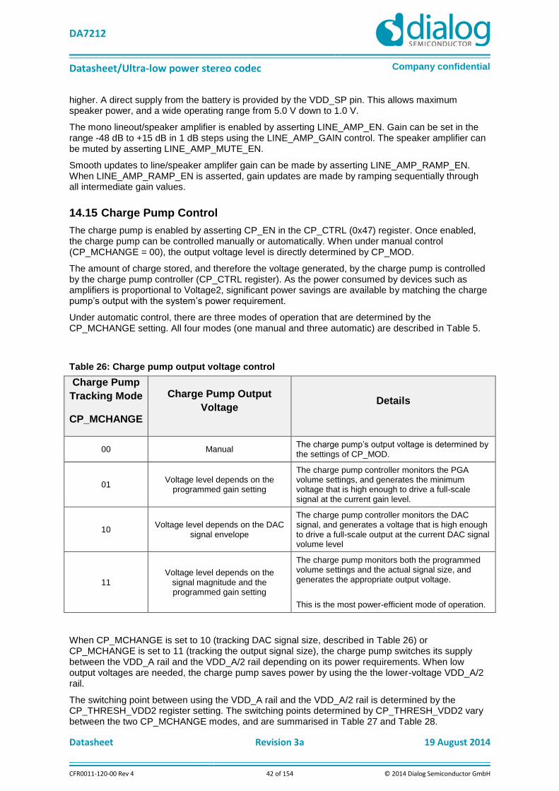
DA7212
Datasheet/Ultra-low power stereo codec Company confidential
Datasheet Revision 3a 19 August 2014
CFR0011-120-00 Rev 4 42 of 154 © 2014 Dialog Semiconductor GmbH
higher. A direct supply from the battery is provided by the VDD_SP pin. This allows maximum speaker power, and a wide operating range from 5.0 V down to 1.0 V.
The mono lineout/speaker amplifier is enabled by asserting LINE_AMP_EN. Gain can be set in the range -48 dB to +15 dB in 1 dB steps using the LINE_AMP_GAIN control. The speaker amplifier can be muted by asserting LINE_AMP_MUTE_EN.
Smooth updates to line/speaker amplifer gain can be made by asserting LINE_AMP_RAMP_EN. When LINE_AMP_RAMP_EN is asserted, gain updates are made by ramping sequentially through all intermediate gain values.
Charge Pump Control 14.15
The charge pump is enabled by asserting CP_EN in the CP_CTRL (0x47) register. Once enabled, the charge pump can be controlled manually or automatically. When under manual control (CP_MCHANGE = 00), the output voltage level is directly determined by CP_MOD.
The amount of charge stored, and therefore the voltage generated, by the charge pump is controlled by the charge pump controller (CP_CTRL register). As the power consumed by devices such as amplifiers is proportional to Voltage2, significant power savings are available by matching the charge pump’s output with the system’s power requirement.
Under automatic control, there are three modes of operation that are determined by the CP_MCHANGE setting. All four modes (one manual and three automatic) are described in Table 5.
Table 26: Charge pump output voltage control
Charge Pump
Tracking Mode
CP_MCHANGE
Charge Pump Output
Voltage Details
00 Manual The charge pump’s output voltage is determined by the settings of CP_MOD.
01 Voltage level depends on the
programmed gain setting
The charge pump controller monitors the PGA volume settings, and generates the minimum voltage that is high enough to drive a full-scale signal at the current gain level.
10 Voltage level depends on the DAC
signal envelope
The charge pump controller monitors the DAC signal, and generates a voltage that is high enough to drive a full-scale output at the current DAC signal volume level
11 Voltage level depends on the
signal magnitude and the programmed gain setting
The charge pump monitors both the programmed volume settings and the actual signal size, and generates the appropriate output voltage.
This is the most power-efficient mode of operation.
When CP_MCHANGE is set to 10 (tracking DAC signal size, described in Table 26) or CP_MCHANGE is set to 11 (tracking the output signal size), the charge pump switches its supply between the VDD_A rail and the VDD_A/2 rail depending on its power requirements. When low output voltages are needed, the charge pump saves power by using the the lower-voltage VDD_A/2 rail.
The switching point between using the VDD_A rail and the VDD_A/2 rail is determined by the CP_THRESH_VDD2 register setting. The switching points determined by CP_THRESH_VDD2 vary between the two CP_MCHANGE modes, and are summarised in Table 27 and Table 28.

DA7212
Datasheet/Ultra-low power stereo codec Company confidential
Datasheet Revision 3a 19 August 2014
CFR0011-120-00 Rev 4 43 of 154 © 2014 Dialog Semiconductor GmbH
Note 17 When the charge pump output voltage is controlled manually (CP_MCHANGE = 00) or when it is tracking the PGA gain settings (CP_MCHANGE = 01), the charge pump always takes its supply from VDD_A
Table 27: CP_THRESH_VDD2 Settings in DAC_VOL mode (CP_MCHANGE = 10)
CP_THRESH_VDD2 Setting Approximate Switching
Point Notes
0x01 -30 dBFS Do not use. Very power-inefficient as nearly always VDD/1
0x03 -24 dBFS Not recommended. Very power-inefficient as nearly always VDD/1
0x07 -18 dBFS Good to use but not power efficient
0x0E -12 dBFS Good to use
0x10 -10 dBFS Recommended setting
0x3F – 0x13 Not recommended
Note 18 Full Scale (FS) = 1.6 * VDD_A
Table 28: CP_THRESH_VDD2 Settings in Signal Size mode (CP_MCHANGE = 11)
CP_THRESH_VDD2 Setting Approximate Switching Point Notes
0x00 Never Not recommended. Always VDD/1 mode
0x01 Never Not recommended. Always VDD/1 mode
0x02 -32 dBFS Not recommended. Very power-inefficient as nearly always VDD/1
0x03 -24 dBFS Good to use
0x04 -20 dBFS Good to use
0x05 -17 dBFS Good to use
0x06 -15 dBFS Recommended setting
0x07 -13 dBFS Good to use
0x08 -12 dBFS Good to use
0x09 -11 dBFS Good to use
0x0A -10 dBFS Good to use
0x0B -9 dBFS Not recommended. VDD/2 begins to clip
0x0C Never Not recommended. Always VDD/2 mode
0x0D Never Not recommended. Always VDD/2 mode
0x0E Never Not recommended. Always VDD/2 mode
0x0F Never Not recommended. Always VDD/2 mode
Note 19 Full Scale (FS) = 1.6 * VDD_A

DA7212
Datasheet/Ultra-low power stereo codec Company confidential
Datasheet Revision 3a 19 August 2014
CFR0011-120-00 Rev 4 44 of 154 © 2014 Dialog Semiconductor GmbH
Charge pump clock control 14.16
The charge pump on DA7212 requires two clocks (cp_clk and cp_clk2). The cp_clk2 clock runs at a slower frequency than cp_clk. It is cp_clk that actually clocks the charge pump.
To prevent the clocks stopping in an unknown state, there are always two pulses on cp_clk for every one pulse of cp_clk2. This is illustrated in Figure 12.
cp_clk
clk
cp_clk2
Figure 12: Input (clk) and Output Clocks (cp_clk and cp_clk2) at CP_FCONTROL = 010
When CP_ANALOGUE_LVL = 00 (‘No feedback’ – see Section 14.17 for more details), the charge pump’s nominal clock rate cp_clk is controlled by CP_FCONTROL, providing a range from 1 MHz (CP_FCONTROL = 000) down to 63 kHz (CP_FCONTROL = 100). With the slower clock rates, quiescent power consumption is lower but the trade-off is a reduced load current, and slower changes to the voltage.
Section 14.17 describes how quiescent power and load current can be varied according to demand.
Boosting the charge pump using demand feedback control 14.17
When CP_ANALOGUE_LVL = 00, the clock frequency for the charge pump is under direct control of the registers as described in Section 0.
When CP_ANALOGUE_LVL = 01 or 10 (11 is reserved and is not used), the demands on the charge pump output are tracked, and the clock frequency is boosted when necessary to give the required output current.
This gives the benefit of a very low (or even zero) quiescent current when the charge pump is not required combined with a maximum output when that is required.
Tracking the demands on the charge pump output 14.17.1
There are three points at which the demands on the charge pump can be tracked. These tracking points are determined by CP_MCHANGE.
14.17.1.1 CP_MCHANGE = 00 (manual mode)
If CP_MCHANGE = 00, the voltage level is controlled by the CP_MOD setting.
14.17.1.2 CP_MCHANGE = 01 (tracking the PGA gain setting)
If CP_MCHANGE = 01, it is the PGA gain setting that is tracked, and which provides the feedback to boost the clock frequency when necessary.
14.17.1.3 CP_MCHANGE = 10 (tracking the DAC signal setting)
If CP_MCHANGE = 01, it is the size of the DAC signal that is tracked, and which provides the feedback to boost the clock frequency when necessary.
14.17.1.4 CP_MCHANGE = 11 (tracking the output signal magnitude)
If CP_MCHANGE = 01, it is the magnitude of the output signal that is tracked, and which provides

DA7212
Datasheet/Ultra-low power stereo codec Company confidential
Datasheet Revision 3a 19 August 2014
CFR0011-120-00 Rev 4 45 of 154 © 2014 Dialog Semiconductor GmbH
the feedback to boost the clock frequency when necessary.
Specifying clock frequencies when tracking the charge pump output 14.17.2demand
CP_FCONTROL specifies the frequency of the charge pump clock. The frequency is fixed and is set manually if CP_MCHANGE = 00 (see section 14.17.1.1). The available frequency settings are 1 MHz (the absolute maximum), and 500, 250, 125 and 63 kHz.
If CP_MCHANGE not = 00, the charge pump load is monitored and the clock frequency adjusted accordingly to allow the charge pump to supply the required current. Clock frequency varies depending on the charge pump requirements, and the CP_FCONTROL settings specify the minimum frequency at which the clock will run. The maximum frequency is always 1 MHz.
In addition to the CP_FCONTROL settings outlined above, and which specify the minimum clock frequency, there is an extra setting of CP_FCLOCK = 101 which has no minimum frequency. The clock frequency is under the complete control of the tracking and feedback mechanism. The frequency can vary from 0 Hz when there is no load on the charge pump and no component leakage, up to the maximum of 1 MHz.
These settings are all summarised in Table 29.
Controlling the boost of the charge pump clock-frequency 14.17.3
The manner in which the charge pump clock-frequency is boosted is controlled by CP_ANALOGUE_LVL. If CP_ANALOGUE_LVL = 00, there is no feedback to the clock generator, and the frequency remains fixed at the frequency specified by CP_FCONTROL.
14.17.3.1 CP_ANALOGUE_LVL = 01
If CP_ANALOGUE_LVL = 01, the clock frequency is boosted from the base frequency specified in CP_FCONTROL by the insertion of extra clock pulses in to the clock signal as and when required. When no extra pulses are being inserted, the clock frequency remains fixed at the value specified by CP_FCONTROL. The extra clock pulses are inserted in to the clock signal as needed as long as the clock frequency does not exceed its maximum of 1 MHz. These settings are all summarised in Table 29.
.
14.17.3.2 CP_ANALOGUE_LVL = 10
If CP_ANALOGUE_LVL = 10, instead of boosting the clock frequency by inserting extra clock pulses as described in section 14.17.3.1, the clock is restarted. By restarting the clock before the next pulse is due, the frequency is effectively increased. The clock frequency can be increased from the minimum frequency specified in CP_FCONTROL, up to the maximum frequency of 1 MHz. These settings are all summarised in Table 29.
.

DA7212
Datasheet/Ultra-low power stereo codec Company confidential
Datasheet Revision 3a 19 August 2014
CFR0011-120-00 Rev 4 46 of 154 © 2014 Dialog Semiconductor GmbH
Table 29: Charge pump current load control
CP_ANALOGUE_LVL (0x47[1:0])
00
No current boost
01
Variable current boost
10
Variable current boost
11
CP_FCONTROL
(0x96[2:0])
000 1 MHz 1 MHz 1 MHz Reserved
001 500 kHz
From 500 kHz to1MHz depending on demand Note 20
From 500 kHz to1MHz depending on demand Note 20
Reserved
010 250 kHz
From 250 kHz to1MHz depending on demand Note 20
From 250 kHz to1MHz depending on demand Note 20
Reserved
011 125 kHz
From 125 kHz to1MHz depending on demand Note 20
From 125 kHz to1MHz depending on demand Note 20
Reserved
100 63 kHz
From 63 kHz to1MHz depending on demand Note 20
From 63 kHz to1MHz depending on demand Note 20
Reserved
101 Reserved
0 Hz to 1MHz depending on
demand Note 20
0 Hz to 1MHz depending on
demand Note 20 Reserved
110 Reserved
Reserved Reserved Reserved
111 Reserved Reserved Reserved Reserved
Note 20 Power demand is determined bythe PGA gain level if CP_MCHANGE = 01, by the DAC signal level if CP_MCHANGE = 10 , or by the output signal level If CP_MCHANGE = 11
Other Charge Pump Controls 14.18
When a higher charge pump output voltage is needed, the charge pump increases its output as the fastest rate possible given the controls and settings in that currently in place. Once the higher output voltage is no longer needed, the charge pump controller waits for a period determined by the CP_TAU_DELAY setting before reducing the output voltage. For best performance Dialog recommend setting CP_TAU_DELAY to 16ms or greater.
The charge pump limiter is controlled by CP_ON_OFF. The limiter restricts the current flow to the charge pump’s capacitors at start-up.
CP_SMALL_SWITCH_FREQ_EN enables a low-load, low-power switching mode. If CP_SMALL_SWITCH_FREQ_EN is enabled and CP_FCONTROL is set to a value between 000 and 100, any feedback from the analogue level detector results in a switch from low-power to full-power. Full-power is maintained for one CP_TAU_DELAY period after the pulse. Any subsequent pulses restart the CP_TAU_DELAY period.
If CP_FCONTROL = 101, the first feedback from the analogue level detector primes the change to full-power mode. If another pulse occurs within 32 clock cycles of the first feedback from the analogue level detector, full power is enabled for one CP_TAU_DELAY period.
Digital Signal Processing Engine 14.19
The digital signal processing engine includes a configurable audio processor that offers flexible routing and extensive audio enhancement and effects. Linear phase FIR filters perform the DAC

DA7212
Datasheet/Ultra-low power stereo codec Company confidential
Datasheet Revision 3a 19 August 2014
CFR0011-120-00 Rev 4 47 of 154 © 2014 Dialog Semiconductor GmbH
interpolation and decimation for the required sample rates. Configurable high-pass filtering (optionally enabled on both ADC and DAC) removes any signal DC offset and can help to filter out wind noise. A 5-band playback equaliser can be configured to suit the users listening preferences.
Variable High Pass Audio Filter (DC Cut) 14.20
Any DC offset from the input path is removed via IIR filters (typically <2Hz roll-off, configurable). After reset the filters for both channels are enabled by default, but can be disabled by clearing ADC_HPF_EN and DAC_HPF_EN. The cutoff frequency of the filters can be programmed using ADC_AUDIO_HPF_CORNER and DAC_AUDIO_HPF_CORNER. Enabling the high pass filter is especially important if the ADC output is fed into the DAC.
Table 30: ADC/DAC Digital High Pass Filter specifications in Audio Mode
Sampling Frequency
(kHz)
Cut-off frequency (Hz) at
ADC_AUDIO_HPF_CORNER and
DAC_AUDIO_HPF_CORNER Settings
00 01 10 11
8 0.3 0.7 1.3 2.7
11.025 0.4 0.9 1.8 3.7
12 0.5 1 2 4
16 0.7 1.3 2.7 5.3
22.05 0.9 1.8 3.7 7.3
24 1 2 4 8
32 1.3 2.7 5.3 10.7
44.1 1.8 3.7 7.3 14.7
48 2 4 8 16

DA7212
Datasheet/Ultra-low power stereo codec Company confidential
Datasheet Revision 3a 19 August 2014
CFR0011-120-00 Rev 4 48 of 154 © 2014 Dialog Semiconductor GmbH
Figure 13: ADC and DAC DC blocking (Cut-off frequency setting ‘00’ to ‘11’, 16 kHz)
Variable High Pass Filter (Wind Noise Filtering) 14.21
To improve the quality of microphone recordings, the DA7212 provides a programmable high pass filter engine, enabled via ADC_VOICE_EN. The low frequency roll off is configured over a wide range using the ADC_VOICE_HPF_CORNER control. This allows for flexible removal of wind and pop noise.
During playback, dedicated voiceband filtering can be enabled using DAC_VOICE_EN. The low frequency roll off is configured over a wide range using the DAC_VOICE_HPF_CORNER control.
In Voice mode, the wind noise high-pass filter cut-off frequency is determined by the settings of the ADC_VOICE_HPF_CORNER and the DAC_VOICE_HPF_CORNER register bits, These cut-off frequencies are not fixed, however, and vary with the sample rate being used. Table 31 shows the cut-off frequencies for all valid settings of ADC_VOICE_HPF_CORNER and DAC_VOICE_HPF_CORNER, at all sample rates of 16 kHz and below.
Table 31: Wind noise high-pass filter specifications
Cut-off frequency at ADC_VOICE_HPF_CORNER and DAC_VOICE_HPF_CORNER settings
(Voice Filtering only, and with Sample Rate 16 kHz or lower)
Fs [kHz] 000 001 010 011 100 101 110 111
8.0 2.5 25 50 100 150 200 300 400
11.025 3.4 34.5 69 138 207 276 413 551
12.0 3.75 37.5 75 150 225 300 450 600
16.0 5 50 100 200 300 400 600 800

DA7212
Datasheet/Ultra-low power stereo codec Company confidential
Datasheet Revision 3a 19 August 2014
CFR0011-120-00 Rev 4 49 of 154 © 2014 Dialog Semiconductor GmbH
Figure 14: Wind noise high-pass filter (cut-off frequency setting ‘000’ to ‘111’, 16 kHz)
DAC 5-Band Equaliser 14.22
To enable user controllable listening preferences, the digital playback path includes a programmable 5 band equaliser that is enabled by control DAC_EQ_EN. A low pass filter, a three band-pass filters and a high pass filter with cut-off/centre frequencies at approximately 87Hz, 132Hz, 628Hz, 2.6 kHz and 9.6 kHz (for FS=48 kHz) offer boosting or damping of each frequency band in 1.5 dB steps from 10.5 to +12 dB. The gains of each band can be individually configured using DAC_EQ_BAND1, DAC_EQ_BAND2, DAC_EQ_BAND3, DAC_EQ_BAND4, DAC_EQ_BAND5 controls.
The 5-band equaliser cannot be used at 88.2 and 96 kHz sampling rate. For frequency responses see Table 9, and Figure 15 to Figure 19.

DA7212
Datasheet/Ultra-low power stereo codec Company confidential
Datasheet Revision 3a 19 August 2014
CFR0011-120-00 Rev 4 50 of 154 © 2014 Dialog Semiconductor GmbH
Table 32: DAC 5-Band Equaliser Turnover/Centre Frequencies
Sampling
Frequency (kHz)
Centre/Cutoff frequency of DAC 5-Band Equaliser (Hz)
Band 1
Cutoff (Note
21)
Band 2
Centre
Band 3
Centre
Band 4
Centre
Band 5
Cutoff (Note
21)
8 21 85 563 1151 2909
11.025 29 117 776 2137 4009
12 31 128 845 2326 4364
16 41 90 441 2128 5840
22.05 56 124 607 2933 8048
24 61 135 664 3192 8759
32 58 95 418 1731 6374
44.1 80 132 577 2385 8784
48 87 143 628 2596 9560
88.2 N/A N/A N/A N/A N/A
96 N/A N/A N/A N/A N/A
Note 21 For equaliser bands 1 and 5, the cut-off frequency depends on the gain setting. The figures quoted in this table refer to the –1 dB point with the band gain set to –3 dB
Figure 15: Equaliser filter Band 1 frequency response at FS = 48 kHz

DA7212
Datasheet/Ultra-low power stereo codec Company confidential
Datasheet Revision 3a 19 August 2014
CFR0011-120-00 Rev 4 51 of 154 © 2014 Dialog Semiconductor GmbH
Figure 16: Equaliser filter Band 2 frequency response at FS = 48 kHz
Figure 17: Equaliser filter Band 3 frequency response at FS = 48 kHz

DA7212
Datasheet/Ultra-low power stereo codec Company confidential
Datasheet Revision 3a 19 August 2014
CFR0011-120-00 Rev 4 52 of 154 © 2014 Dialog Semiconductor GmbH
Figure 18: Equaliser filter Band 4 frequency response at FS = 48 kHz
Figure 19: Equaliser filter Band 5 frequency response at FS = 48 kHz
Soft Mute 14.23
To improve the user’s perception of audio reconfigurations, the DAC channel signals may be soft muted by asserting the control DAC_SOFTMUTE_EN. The soft mute function attenuates the digital input to the DAC, ramping the gain down in steps of 0.1875 dB from its current level to -77.25 dB, then completely muting the channel. When DAC_SOFTMUTE_EN is released, the attenuation is set to 77.25 dB, and then ramped up to the previous gain level. Both left and right channels of Soft Mute enabled output amplifiers are muted simultaneously. The ramping up and down rate is dependent on the audio sample rate and can be individually configured using control DAC_SOFTMUTE_RATE.
Note 22 Please note that during active soft muting, the digital gain of the DAC will be different to the value programmed inside controls DAC_L_DIGITAL_GAIN and DAC_R_DIGITAL_GAIN.

DA7212
Datasheet/Ultra-low power stereo codec Company confidential
Datasheet Revision 3a 19 August 2014
CFR0011-120-00 Rev 4 53 of 154 © 2014 Dialog Semiconductor GmbH
Playback Noise-Gate 14.24
Noise-Gate is an automatic gain control for DAC playback that reduces the noise heard during playback if no signal is present. It is enabled using the DAC_NG_EN control.
When the output signals on both channels are below a given threshold level, and they stay low for longer than a specified period, then playback noise-gate is activated. When the playback noise-gate activates, the gain on the active HP and Line amplifiers are ramped down to their lowest levels. This is equivalent to asserting the minimum-gain controls HP_L_AMP_MIN_GAIN_EN, HP_R_AMP_MIN_GAIN_EN and LINE_AMP_MIN_GAIN_EN.
The Noise-Gate Threshold Level can be specified in 6 dB steps from 90 dB to 48 dB. The Noise-Gate Threshold Time ranges from 256 samples to 2048 samples and is set using the control DAC_NG_SETUP_TIME.
When the averaged level of the two channels exceeds the release threshold configured in DAC_NG_OFF_THRESHOLD, the gain of the amplifiers is ramped up back to its original value. When the average level of the two channels is below the attack threshold configured in DAC_NG_ON_THRESHOLD for longer than the time specified in DAC_NG_SETUP_TIME, the gain is ramped down to its minimum value.
The attack and release rate can be configured via controls DAC_NG_RAMPDN_RATE and DAC_NG_RAMPUP_RATE. The Noise-gate release time is usually much faster than the attack time, to allow a proper playback as soon as a signal is present at the output amplifiers.
Clock Modes 14.25
The DA7212 requires a clock for operation of various circuits within the chip. There are four ways in which the main system clock may be generated:
PLL bypass mode: If digital playback or record is required, the MCLK frequency should be set to one of 11.2896/12.288 MHz or 22.5792/24.576 MHz or 45.1584/49.152 MHz (Note 23). The PLL_INDIV register bit must then be programmed accordingly
Normal PLL mode: Alternative frequency clock applied to MCLK pin (in the range of 2 to 50 MHz), where MCLK is synchronous with WCLK, or Master Mode is enabled
SRM PLL mode: Clock applied to MCLK pin (in the range of 2 to 50 MHz) is asynchronous to WCLK
32 kHz mode: Watch crystal frequency (32.768 kHz) clock applied to MCLK
32 kHz mode: Watch crystal frequency (32.768 kHz) clock applied to MCLK
Note 23 11.2896 MHz (or multiples) should be used as MCLK frequency for 11.025, 22.05, 44.1, 88.2 kHz sample rates and 12.288 MHz (or multiples) should be used for 8, 12, 16, 24, 32, 48, 96 kHz sample rates
Mode PLL bypassed PLL enabled PLL enabled SRM
enabled
PLL enabled 32 kHz
enabled
Master Yes (Note 24) Yes (Note 25) No Yes (Note 26)
Slave Yes (Note 27) Yes (Note 28) Yes (Note 29) No
Note 24 11.2896 MHz (or multiples) should be used as MCLK frequency for 11.025, 22.05, 44.1, 88.2 kHz sample rates and 12.288 MHz (or multiples) should be used for 8, 12, 16, 24, 32, 48, 96 kHz sample rates

DA7212
Datasheet/Ultra-low power stereo codec Company confidential
Datasheet Revision 3a 19 August 2014
CFR0011-120-00 Rev 4 54 of 154 © 2014 Dialog Semiconductor GmbH
Note 25 MCLK must be exactly 12.288 MHz or 11.2896 MHz or a multiple thereof
Note 26 MCLK must be between 2 MHz and 50 MHz
Note 27 MCLK must be 32.768 kHz
Note 28 MCLK must be exactly 12.288 MHz or 11.2896 MHz or a multiple thereof and synchronous with BCLK and WCLK
Note 29 MCLK must be synchronous with BCLK and WCLk
Note 30 BCLK must be synchronous with WCLK. MCLK must be between 2 MHz and 50 MHz
With the default register settings, the clock input should be a square wave with CMOS logic levels (referenced to VDD_IO). A ‘clock squarer circuit’ can be enabled by asserting the PLL_MCLK_SQR_EN register bit. This clock squarer allows a sine wave or other a low amplitude clock (down to 300 mVpp) to be applied to the codec. The input is AC coupled on chip when using the clock squarer mode.
If the MCLK input frequency drops below 1 MHz, the PLL_MCLK_STATUS bit is cleared, and the chip will automatically use its internal reference oscillator as a clock source.
PLL Bypass Mode 14.26
If an MCLK signal at 11.2896/12.288 MHz or 22.5792/24.576 MHz or 45.1584/49.152 MHz is available, the PLL is not required and should be disabled to save power. PLL bypass mode is activated by clearing the PLL enable register bit PLL_EN.
In this mode the PLL is bypassed and an audio frequency clock is applied to the MCLK pin of the codec. The required clock frequency depends on the sample rate at which the audio DACs and ADCs are operating. These clock frequencies are summarized in Table 33 for the range of DAC and ADC sample rates that can be configured using the SR register.
Table 33: Sample rate control register and corresponding system clock frequency
Sample rate, FS (kHz) SR Register System clock
frequency (MHz)
8 0001 12.288
11.025 0010 11.2896
12 0011 12.288
16 0101 12.288
22.05 0110 11.2896
24 0111 12.288
32 1001 12.288
44.1 1010 11.2896
48 1011 12.288
88.2 1110 11.2896
96 1111 12.288
If digital playback or record is required in bypass mode then the MCLK frequency should be set to 11.2896/12.288 MHz, or to 22.5792/24.576 MHz, or to 45.1584/49.152 MHz and PLL_INDIV should be programmed accordingly.
If no valid MCLK is detected, the output of the internal reference oscillator is used instead. However in this case only analogue bypass paths may be used.

DA7212
Datasheet/Ultra-low power stereo codec Company confidential
Datasheet Revision 3a 19 August 2014
CFR0011-120-00 Rev 4 55 of 154 © 2014 Dialog Semiconductor GmbH
Normal PLL Mode (DAI Master) 14.26.1
The DA7212 contains a Phase Locked Loop (PLL) that can be used to generate the required 11.2896
MHz or 12.288 MHz internal system clock when a frequency of between 2 and 50 MHz is applied to
MCLK. This allows sharing of clocks between devices in an application, reducing total system cost.
For example, the codec may operate from common 13 MHz or 19.2 MHz system clock frequency.
The PLL is enabled by asserting PLL_EN. Once the PLL is enabled and has achieved phase lock, PLL
Bypass Mode is disabled, and the output of the PLL is used as the system clock.
The PLL Input Divider register (PLL_INDIV) is used to reduce the PLL reference frequency to the
usable range of 2 to 5 MHz as shown in Table 12. PLL_INDIV reduces the PLL Reference Frequency
according to the following equation:
FREF = FMCLK ÷ (2^PLL_INDIV)
Table 34: PLL Input Divider
MCLK input frequency (MHz) Input divider, (÷N) PLL_INDIV Register (0x27 [3:2])
2 – 10 ÷2 00
10 – 20 ÷4 01
20 – 40 ÷8 10
40 – 50 ÷16 11
The value of the PLL Feedback Divider is used to set the Voltage Controlled Oscillator (VCO) frequency to 8 times the required system clock frequency (see Table 35)
FVCO = FREF × PLL Feedback Divider
The value of the PLL Feedback Divider is an unsigned number in the range of 0 to 128. It consists of seven integer bits and 13 fractional bits split across three registers:
PLL_INTEGER holds the seven integer bits
PLL_FRAC_TOP holds the top bits (MSB) of the fractional part of the divisor
PLL_FRAC_BOT holds the bottom bits (LSB) of the fractional part of the divisor
Example calculation of the Feedback Divider setting: 14.26.2
We will use as an example a codec operating with Fs (sample rate) = 48 kHz and an Reference Input Clock frequency of 12.288 MHz. The required output frequency is 98.304 MHz.
The Reference Clock Input = 12.288 MHz, which falls in the range 10-20 MHz so PLL_INDIV must be set to 0b01 (dividing the Reference Input Frequency by 2 - see Table 12: PLL Input Divider.
The formula for calculating the Feedback Divider is:
Feedback Divider (F) = VCO output frequency * Input Divider (PLL_INDIV) / Reference Input Clock

DA7212
Datasheet/Ultra-low power stereo codec Company confidential
Datasheet Revision 3a 19 August 2014
CFR0011-120-00 Rev 4 56 of 154 © 2014 Dialog Semiconductor GmbH
Feedback Divider = (98.304 * 4) / 12.288 = 32
So
PLL_FBDIV_INTEGER (holding the seven integer bits) = 0x20
PLL_FBDIV_FRAC_TOP (holding the top bits (MSB) of the fractional part of the divisor) = 0x00
PLL_FBDIV_FRAC_BOT (holding the bottom bits (LSB) of the fractional part of the divisor) = 0x00
Table 37 (below) shows example register settings that will configure the PLL when using a 13 MHz, 15 MHz or 19.2 MHz clock. Note that any MCLK input frequency between 2 and 50 MHz is supported. PLL_INDIV must be used to reduce the PLL reference frequency to the usable range of 2 to 10 MHz as shown in Table 13.
Table 35: Example PLL configurations
MCLK input
frequency
(MHz)
System
clock
frequency
(MHz)
PLL_CTRL
Register
(See Note
31 below)
PLL_FRAC_TOP
Register
PLL_FRAC_BOT
Register
PLL_INTEGER
Register
13 11.2896 0x84 0x19 0x45 0x1B
13 12.288 0x84 0x07 0xEA 0x1E
15 11.2896 0x84 0x02 0xB4 0x18
15 12.288 0x84 0x06 0xDC 0x1A
19.2 11.2896 0x84 0x1A 0x1C 0x12
19.2 12.288 0x84 0x0F 0x5C 0x14
Note 31 Note: Any MCLK input frequency between 2 and 50 MHz is supported. PLL_INDIV must be used to reduce the PLL reference frequency to the usable range of 2 to 5 MHz.
SRM PLL Mode (DAI Slave) 14.27
SRM mode enables the PLL output clock to be synchronized to the incoming WCLK signal on the DAI. The SRM PLL mode is enabled by setting the PLL as for normal PLL mode and asserting register bit PLL_SRM_EN. Register bit SRM_LOCK indicates whether or not the SRM has achieved synchronisation with WCLK.
Note 32 When using the digital audio interface in slave mode with the SRM enabled, removing and re-applying the DAI interface word clock WCLK may cause the PLL lock to be lost. To re-lock the PLL it is recommended that you disable the SRM (PLL_SRM_EN = 0), reset the PLL by re-writing to register PLL_INTEGER, and then re-enable the SRM (PLL_SRM_EN = 1) after the DAI WCLK has been reapplied.
Note 33 When switching sample rates between 44.1 kHz and 48 kHz (or between the multiples of these sample rates), SRM must be disabled and then re enabled using register bit PLL_SRM_EN.
32 kHz PLL Mode (DAI Master) 14.28
32 kHz mode enables the PLL output clock to be synchronized to a 32.768 kHz clock signal on the MCLK pin. 32 kHz PLL Mode is selected by enabling the PLL and asserting both PLL_SRM_EN and PLL_32K_MODE. Register bit SRM_LOCK indicates whether or not the SRM has achieved synronisation with MCLK.

DA7212
Datasheet/Ultra-low power stereo codec Company confidential
Datasheet Revision 3a 19 August 2014
CFR0011-120-00 Rev 4 57 of 154 © 2014 Dialog Semiconductor GmbH
Operating with a 2 MHz to 5 MHz MCLK 14.28.1
Note that when using the PLL with a 2 MHz-5 MHz MCLK, you must follow the procedure below to setup the PLL in the correct mode.
Setup PLL and clocking
Write F0 = 8b
Write F1 = 03
Write F0 = 00
When returning from this mode to a mode with an MCLK >5 MHz, you must follow the procedure below.
Write F0 = 8b
Write F1 = 01
Write F0 = 00
Setup PLL and clocking
Mixed Sample Rates 14.29
In DA7212 there is only one Sample Rate register and therefore, by default, this controls the sample rate of both the ADC and the DAC
Some applications require the ADC and the DAC to run at different sample rates. A special mode (24-48 Mode) is available by asserting 24_48_MODE at register address 0x84[0]. Asserting this bit sets the ADC to run at 24kHz and the DAC to run at 48kHz. In this mode all the functionality of the ADC and the DAC is available. The DAI will continue to run at 48kHz, and every ADC sample will be repeated across two WCLK frames.
I2C Control Interface 14.30
The DA7212 is completely software-controlled from the host by registers. The DA7212 provides an I2C compliant serial control interface to access these registers. Data is shifted into or out of the DA7212 under the control of the host processor, which also provides the serial clock.
The 7-bit I2C slave address is 0x1A so that the 8-bit address for writing is 0x34 and for reading is 0x35.
The I2C clock is supplied by the SCL line and the bi directional I2C data is carried by the SDA line. The I2C interface is open-drain supporting multiple devices on a single line. The bus lines have to be pulled HIGH by external pull-up resistors (1 kΩ to 20 kΩ range). The attached devices only drive the bus lines LOW by connecting them to ground. This means that two devices cannot conflict if they drive the bus simultaneously.
In standard/fast mode the highest frequency of the bus is 1 MHz. The exact frequency can be determined by the application and does not have any relation to the DA7212 internal clock signals. DA7212 will follow the host clock speed within the described limitations and does not initiate any clock arbitration or slow down.
In high-speed mode the maximum frequency of the bus can be increased up to 3.4 MHz. This mode is supported if the SCL line is driven with a push-pull stage from the host and if the host enables an external 3mA pull-up at the SDA pin to decrease the rise time of the data. In this mode the SDA line on DA7212 is able to sink up to 12mA. In all other respects the high speed mode behaves as the standard/fast mode. Communication on the I2C bus always takes place between two devices, one acting as the master and the other as the slave. The DA7212 will only operate as a SLAVE. The I2C interface has direct access to the whole register map of the DA7212.

DA7212
Datasheet/Ultra-low power stereo codec Company confidential
Datasheet Revision 3a 19 August 2014
CFR0011-120-00 Rev 4 58 of 154 © 2014 Dialog Semiconductor GmbH
Host
Processor
CodecSDA
SCL
Peripheral
Device
SDA
SCL
SCL
SDA
VDD_IO
VDD_IO
Figure 20: Schematic of the I2C control interface bus
Details of the I2C Control interface protocol 14.31
All data is transmitted across the I2C bus in groups of 8 bits. To send a bit the SDA line is driven to the intended state while the SDA is LOW (a LOW on SDA indicates a zero bit). Once the SDA has settled, the SCL line is brought HIGH and then LOW. This pulse on SCL clocks the SDA bit into the receiver’s shift register.
A two byte serial protocol is used containing one byte for address and one byte for data. Data and address transfer is transmitted MSB first for both read and write operations. All transmission begins with the START condition from the master while the bus is in the IDLE state (the bus is free). It is initiated by a high to low transition on the SDA line while the SCL is in the high state (a STOP condition is indicated by a low to high transition on the SDA line while the SCL line is in the high state).
SCL
SDA
Figure 21 Timing of I2C START and STOP Conditions
The I2C bus is monitored by DA7212 for a valid SLAVE address whenever the interface is enabled. It responds with an Acknowledge immediately when it receives its own slave address. The Acknowledge is done by pulling the SDA line low during the following clock cycle (white blocks marked with ‘A’ in Figure 22 to Figure 25).
The protocol for a register write from master to slave consists of a start condition, a slave address
with read/write bit and the 8-bit register address followed by 8 bits of data terminated by a STOP
condition (the DA7212 responds to all bytes with Acknowledge). This is illustrated in Figure 22.

DA7212
Datasheet/Ultra-low power stereo codec Company confidential
Datasheet Revision 3a 19 August 2014
CFR0011-120-00 Rev 4 59 of 154 © 2014 Dialog Semiconductor GmbH
SLAVE addr W REG addr A DATA A P
S = START condition A = Acknowledge (low) P = STOP condition W = Write (low)
Master to Slave Slave to Master
7-bits 1-bit 8-bits 8-bits
A S
Figure 22: I2C Byte write (SDA signal)
When the host reads data from a register it first has to write-access DA7212 with the target register address and then read access DA7212 with a repeated START, or alternatively a second START condition. After receiving the data the host sends a Not Acknowledge (NAK) and terminates the transmission with a STOP condition:
S SLAVEaddr W A REG addr A SLAVEaddr A
S = START condition A = Acknowledge (low)
Sr = Repeated START condition A* = Not Acknowledge (NAK)
P = STOP condition W = Write (low) R = Read (high)
Master to Slave
7-bits 1-bit 8-bits 7-bits
DATA A* Sr R
1-bit 8-bits
SLAVEaddr A
7-bits
DATA P S R
1-bit 8-bits
P
A*
Slave to Master
S SLAVEaddr W A REG addr P
7-bits 1-bit 8-bits
A
Figure 23: Examples of the I2C Byte Read (SDA line)
Consecutive (Page Mode) read-out mode (CIF_I2C_WRITE_MODE (0x1D [0]) = 0) is initiated from the master by sending an Acknowledge instead of Not Acknowledge (NAK) after receipt of the data word. The I2C control block then increments the address pointer to the next I2C address and sends the data to the master. This enables an unlimited read of data bytes until the master sends a NAK directly after the receipt of data, followed by a subsequent STOP condition. If a non-existent I2C address is read out, the DA7212 will return code zero.
S SLAVEaddr W A REG addr A SLAVEaddr A
S = START condition A = Acknowledge (low) Sr = Repeat START condition A
* = Not Acknowledge (NAK)
P = STOP condition W = Write (low) R = Read (high)
Master to Slave Slave to Master
7-bits 1 bit 8-bits 7-bits
DATA A
Sr R
1-bit 8-bits
S SLAVEaddr W A REG addr A SLAVEaddr A
7-bits 1-bit 8-bits 7-bits
DATA P S R
1-bit 8-bits
P A
A*
P DATA DATA A
A*
DATA
8-bits
8-bits 8-bits
Figure 24: Examples of I2C Page Read (SDA line)
Note 1 The slave address after the Repeated START condition must be the same as the previous slave address
Consecutive write-mode (CIF_I2C_WRITE_MODE (0x1D [0]) = 0) is supported if the Master sends several data bytes following a slave register address. The I2C control block then increments the address pointer to the next I2C address, stores the received data and sends an Acknowledge until the master sends the STOP condition.

DA7212
Datasheet/Ultra-low power stereo codec Company confidential
Datasheet Revision 3a 19 August 2014
CFR0011-120-00 Rev 4 60 of 154 © 2014 Dialog Semiconductor GmbH
S SLAVEaddr W A REGadr A DATA A
S = START condition A = Acknowledge (low) Sr = Repeat START condition A
* = Not Acknowledge (NAK)
P = STOP condition W = Write (low) R = Read (high)
Master to Slave Slave to Master
7-bits 1 bit 8-bits 8-bits
DATA A
1-bit 8-bits
A
P DATA ………. A
8-bits Repeated writes
Figure 25: I2C Page Write (SDA Line)
An alternative repeated-write mode that uses non-consecutive slave register addresses is available using the CIF_I2C_WRITE_MODE register. In this Repeat Mode (CIF_I2C_WRITE_MODE (0x1D [0]) = 1), the slave can be configured to support a host’s repeated write operations into several non-consecutive registers. Data is stored at the previously received register address. If a new START or STOP condition occurs within a message, the bus returns to IDLE mode. This is illustrated in Figure 26

DA7212
Datasheet/Ultra-low power stereo codec Company confidential
Datasheet Revision 3a 19 August 2014
CFR0011-120-00 Rev 4 61 of 154 © 2014 Dialog Semiconductor GmbH
S SLAVEaddr W A REG addr A DATA A
S = START condition A = Acknowledge (low) Sr = Repeat START condition A
* = Not Acknowledge (NAK)
P = STOP condition W = Write (low) R = Read (high)
Master to Slave Slave to Master
7-bits 1 bit 8-bits 8-bits
REG addr A
1-bit 8-bits
A
P DATA ………. A
8-bits Repeated writes
Figure 26: I2C Repeated Write (SDA Line)
Note 2 Note that in Page Mode (CIF_I2C_WRITE_MODE = 0), both Page Mode reads and writes using auto-incremented addresses, and Repeat Mode reads and writes using non auto-incremented addresses, are supported. In Repeat Mode (CIF_I2C_WRITE_MODE = 1) however, only Repeat Mode reads and writes are supported.
Digital Audio Interface (DAI) 14.32
DA7212 provides one Digital Audio Interface (DAI) to input DAC data or to output ADC data. It is enabled by asserting DAI_EN. The DSP provides flexible routing options allowing each interface to be connected to different signal paths as desired in each application.
The DAI consists of a four-wire serial interface, with bit clock (BCLK), word clock (WCLK), data-in (DATIN) and data-out (DATOUT) pins. Both master and slave clock modes are supported by the DA7212. Master mode is enabled setting register DAI_CLK_EN (0x28[7]) = 1. In master mode, the bit clock and word clock signals are outputs from the codec. In slave mode these are inputs to the codec.
DA7212
CodecProcessor
BCLK
WCLK
DATIN
DATOUT
Figure 27: Master Mode (DAI_CLK_EN = 1)

DA7212
Datasheet/Ultra-low power stereo codec Company confidential
Datasheet Revision 3a 19 August 2014
CFR0011-120-00 Rev 4 62 of 154 © 2014 Dialog Semiconductor GmbH
DA7212
CodecProcessor
BCLK
WCLK
DATIN
DATOUT
Figure 28: Slave Mode (DAI_CLK_EN = 0)
The internal serialized DAI data is 24 bits wide. Serial data that is not 24 bits wide is either shortened or zero-filled at input to, or at output from, the DAI’s internal 24-bit data width. The serial data word length can be configured to be 16, 20, 24 or 32 bits wide using the DAI_WORD_LENGTH register bits.
Four different data formats are supported by the digital audio interface. The data format is determined by the setting of the DAI_FORMAT register bits.
I2S mode
Left Justified mode
Right Justified mode
DSP mode
Time division multiplexing (TDM) is available in any of these modes to support the case where multiple devices are communicating simultaneously on the same bus. TDM is enabled by asserting the DAI_TDM_MODE_EN bit.

DA7212
Datasheet/Ultra-low power stereo codec Company confidential
Datasheet Revision 3a 19 August 2014
CFR0011-120-00 Rev 4 63 of 154 © 2014 Dialog Semiconductor GmbH
I2S Mode 14.33
In I2S mode (DAI_FORMAT = 0), the MSB of the left channel is valid on the second rising edge of the bit clock after the falling edge of the word clock. The MSB of the right channel is valid on the second rising edge of the bit clock after the rising edge of the word clock, and the MSB of the left channel is valid on the second rising edge of the bit clock after the falling edge of the word clock.
BCLK
WCLK
msb Right Channel lsb msb Left Channel lsbDATIN/DATOUT msb
WCLK 1 = RIGHT CHANNEL DATA WCLK 0 = LEFT CHANNEL DATA
Figure 29: I2S Mode
Left Justified Mode 14.34
In left-justified mode (DAI_FORMAT = 1), the MSB of the right channel is valid on the rising edge of the bit clock following the falling edge of the word clock. The MSB of the left channel is valid on the rising edge of the bit clock following the rising edge of the word clock.
BCLK
WCLK
msb Left Channel lsb msb Right Channel lsbDATIN/DATOUT msb
WCLK 1 = LEFT CHANNEL DATA WCLK 0 = RIGHT CHANNEL DATA
Figure 30: Left Justified Mode
Right Justified Mode 14.35
In right-justified mode (DAI_FORMAT = 2), the LSB of the left channel is valid on the rising edge of the bit clock preceding the falling edge of word clock. The LSB of the right channel is valid on the rising edge of the bit clock preceding the rising edge of the word clock.
BCLK
WCLK
msb Left Channel lsb msb Right Channel lsbDATIN/DATOUT lsb
WCLK 1 = LEFT CHANNEL DATA WCLK 0 = RIGHT CHANNEL DATA
Figure 31: Right Justified Mode

DA7212
Datasheet/Ultra-low power stereo codec Company confidential
Datasheet Revision 3a 19 August 2014
CFR0011-120-00 Rev 4 64 of 154 © 2014 Dialog Semiconductor GmbH
DSP Mode 14.36
In DSP mode (DAI_FORMAT = 3), the rising edge of the word clock starts the data transfer with the left channel data first and immediately followed by the right channel data. Each data bit is valid on the falling edge of the bit clock.
BCLK
WCLK
msb Left Channel lsb msb Right Channel lsbDATIN/DATOUT msb
The falling edge of WCLK can occur anywhere in this area
The falling edge of WCLK can occur anywhere in this area
BCLK
WCLK
msb Left Channel lsb msb Right Channel lsbDATIN/DATOUT msb
Offset
Figure 32: DSP Mode

DA7212
Datasheet/Ultra-low power stereo codec Company confidential
Datasheet Revision 3a 19 August 2014
CFR0011-120-00 Rev 4 65 of 154 © 2014 Dialog Semiconductor GmbH
Time Division Multiplexing (TDM) Mode 14.37
Time Division Multiplexing (TDM) allows multiple devices to communicate on the same bus without conflicting. TDM mode (DAI_TDM_MODE_EN = 1) is an extension of the DSP and the Left Justified formats (see page 63).
DA7212Codec
Processor
DA7212Codec
Bit
Clo
ck
Wo
rd C
lock
DA
C D
ata
In
AD
C D
ata
Ou
t
Figure 33: TDM Example (slave mode)
BCLK
WCLK
msb Left Channel lsb msb Right Channel lsbDATIN/DATOUT msb
WCLK 1 = LEFT CHANNEL DATA WCLK 0 = RIGHT CHANNEL DATA
BCLK
WCLK
msb Left Channel lsb msb Right Channel lsbDATIN/DATOUT msb
WCLK 1 = LEFT CHANNEL DATA WCLK 0 = RIGHT CHANNEL DATA
Offset
Figure 34: TDM Mode (left justified mode)

DA7212
Datasheet/Ultra-low power stereo codec Company confidential
Datasheet Revision 3a 19 August 2014
CFR0011-120-00 Rev 4 66 of 154 © 2014 Dialog Semiconductor GmbH
A time offset is specified from the normal ‘start of frame’ condition using register bit DAI_OFFSET. Since a different offset may be defined for each device on the bus, they may both communicate without collisions.
In the Left-Justified TDM example illustrated in Figure 34, the left channel data is valid DAI_OFFSET clock cycles after the rising edge of the word clock, and the right channel data is valid the same DAI_OFFSET number of clock cycles after the falling edge of the word clock.
In DSP TDM mode (not illustrated), the left channel data is valid after the same DAI_OFFSET clock cycles from the rising edge of the word clock, but the right channel data is valid immediately after the left channel data.
The serial data pin must be tri-stated whenever the output is not valid.
Mono mode is supported in the TDM mode by asserting DAI_MONO_MODE_EN. If DAI_MONO_MODE_EN is asserted, only the data from the Digital Audio Interface left channel is transmitted.
Configuration of the Digital Audio Interface 14.37.1
The data format is configured using register DAI_FORMAT. The offset applied in TDM mode is configured using register DAI_OFFSET. The word length is configured using register DAI_WORD_LENGTH.
The digital audio interface is enabled using register DAI_EN and the frame length is configured using DAI_BCLKS_PER_WCLK.
When using the digital audio interface in slave mode (DAI_CLK_EN = 0), if the WCLK input is not from the same clock source as the MCLK input, then the SRM PLL mode must be enabled to maintain synchronization.
Pop-Free and Click-Free Start-up using the System Controllers 14.38
DA7212 has two System Controllers that provide pop-free and click-free start-up under most conditions.
Level 1 System Controller (SCL1) 14.38.1
The Level 1 System Controller (SCL1) is automatically activated whenever a sub-system’s enable bit is asserted. SCL1 ensures that the desired component parts are sequenced in the correct order to provide click-free and pop-free start-up.
The following example using the left DAC illustrates SCL1 in operation.
1. When the left DAC is enabled by assertion of the DAC_L_EN register bit (register 0x69[7] )
SCL1 first activates the DAC clocks a.
SCL1 then activates the DSP logic b.
Next, SCL1 activates the analogue DAC c.
Finally, SCL1 ramps up the digital gain d.
In this way, SCL1 helps ensure that the DAC_L start-up is free of pops and clicks.
Note 34 Note, however, that if any dependent functions for a sub-system’s activation have not been enabled, SCL1 will not automatically enable them. This allows you greater control over the sequencing of the sub-system, but it also means that any sub-system can potentially be brought up in such a way that audible artefacts such as pops and clicks are introduced.

DA7212
Datasheet/Ultra-low power stereo codec Company confidential
Datasheet Revision 3a 19 August 2014
CFR0011-120-00 Rev 4 67 of 154 © 2014 Dialog Semiconductor GmbH
Level 2 System Controller (SCL2) 14.38.2
Level 2 System Controller (SCL2) is a higher level controller that provides one-touch activation of standard operating modes. Input or output sub-systems can be activated either singly or in combination. All selected sub-systems will start up in the correct order and without pops or clicks when SCL2 is activated.
First, the desired input sub-systems must be selected by asserting the relevant fields (bits 1 to 7) of the SYSTEM_MODES_INPUT (0x50) register. Similarly, the desired output sub-systems must be selected by asserting the relevant fields (bits 1 to 7) of the SYSTEM_MODES_OUTPUT (0x51) register.
Once the desired sub-systems have been selected, the SCL2 controller is activated by writing ‘1’ to the MODE_SUBMIT register field in either the SYSTEM_MODES_INPUT (0x50) or the SYSTEM_MODES_OUTPUT (0x51) register. It does not matter which of the two MODE_SUBMIT fields is asserted. Both work in the same way, and each will start up both the input and the output sub-systems.
When SCL2 is activated by asserting MODE_SUBMIT, all of the register-writes that are required by the selected sub-systems are performed automatically. Each sub-system is brought up in the correct order to avoid pops and clicks, and within each sub-system, the component parts are brought up in the correct pop-free and click-free sequence.
Note 35 Note that the MODE_SUBMIT field used to start SCL2 is self-clearing, and is automatically reset to ‘0’ once SCL2 has started
SCL1 and SCL2 activity can be monitored using the SCL1_BUSY and SCL2_BUSY bits on the SYSTEM_STATUS (0xE0) register.
Note 36 If the DA7212 device is changed from one playback mode to another, or if it is changed from one record mode to another, the initial mode is closed down first before the second mode is activated. This happens automatically.
Power Supply – Standby Mode 14.39
DA7212 has an ultra-low power standby mode that can be enabled to save power when the device is not in use. Standby Mode is controlled using the SYSTEM_ACTIVE register.
Entering Standby Mode 14.39.1
Standby Mode is activated by writing a ‘0’ to the SYSTEM_ACTIVE register bit. This SYSTEM_ACTIVE register cannot be read when in Standby Mode because the act of reading the bit causes it to be asserted, which causes the Standby Mode to be exited.
When entering Standby Mode, it is important that all audio paths are shut down first because the shut down is abrupt and audio artifacts such as pops and click may be heard. No audio functions are possible during Standby Mode, as the reference oscillator and the reference voltages are both shut down.
Exiting Standby Mode 14.39.2
Standby Mode can be exited by writing a ‘1’ to the SYSTEM_ACTIVE register bit.
Any read or write access to the DA7212 will also cause the SYSTEM_ACTIVE bit to be asserted, but note that the first read or write access may fail because of the time taken to restart the reference
DA7212
Datasheet/Ultra-low power stereo codec Company confidential
Datasheet Revision 3a 19 August 2014
CFR0011-120-00 Rev 4 68 of 154 © 2014 Dialog Semiconductor GmbH
oscillator. It is recommended that Standby Mode is exited by writing to the the SYSTEM_ACTIVE register rather than relying on the automatic assertion of the register by a read or write access.
Read or write accesses to I2C slave addresses other than those used by the DA7212 will not cause Standby Mode to be exited.
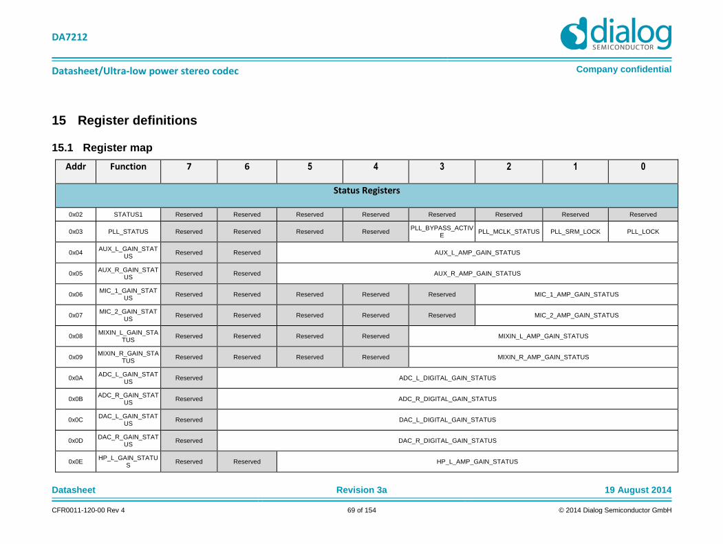
DA7212
Datasheet/Ultra-low power stereo codec Company confidential
Datasheet Revision 3a 19 August 2014
CFR0011-120-00 Rev 4 69 of 154 © 2014 Dialog Semiconductor GmbH
15 Register definitions
Register map 15.1
Addr Function 7 6 5 4 3 2 1 0
Status Registers
0x02 STATUS1 Reserved Reserved Reserved Reserved Reserved Reserved Reserved Reserved
0x03 PLL_STATUS Reserved Reserved Reserved Reserved PLL_BYPASS_ACTIV
E PLL_MCLK_STATUS PLL_SRM_LOCK PLL_LOCK
0x04 AUX_L_GAIN_STAT
US Reserved Reserved AUX_L_AMP_GAIN_STATUS
0x05 AUX_R_GAIN_STAT
US Reserved Reserved AUX_R_AMP_GAIN_STATUS
0x06 MIC_1_GAIN_STAT
US Reserved Reserved Reserved Reserved Reserved MIC_1_AMP_GAIN_STATUS
0x07 MIC_2_GAIN_STAT
US Reserved Reserved Reserved Reserved Reserved MIC_2_AMP_GAIN_STATUS
0x08 MIXIN_L_GAIN_STA
TUS Reserved Reserved Reserved Reserved MIXIN_L_AMP_GAIN_STATUS
0x09 MIXIN_R_GAIN_STA
TUS Reserved Reserved Reserved Reserved MIXIN_R_AMP_GAIN_STATUS
0x0A ADC_L_GAIN_STAT
US Reserved ADC_L_DIGITAL_GAIN_STATUS
0x0B ADC_R_GAIN_STAT
US Reserved ADC_R_DIGITAL_GAIN_STATUS
0x0C DAC_L_GAIN_STAT
US Reserved DAC_L_DIGITAL_GAIN_STATUS
0x0D DAC_R_GAIN_STAT
US Reserved DAC_R_DIGITAL_GAIN_STATUS
0x0E HP_L_GAIN_STATU
S Reserved Reserved HP_L_AMP_GAIN_STATUS

DA7212
Datasheet/Ultra-low power stereo codec Company confidential
Datasheet Revision 3a 19 August 2014
CFR0011-120-00 Rev 4 70 of 154 © 2014 Dialog Semiconductor GmbH
Addr Function 7 6 5 4 3 2 1 0
0x0F HP_R_GAIN_STATU
S Reserved Reserved HP_R_AMP_GAIN_STATUS
0x10 LINE_GAIN_STATU
S Reserved Reserved LINE_AMP_GAIN_STATUS
System Initialisation Registers
0x1D CIF_CTRL CIF_REG_SOFT_
RESET Reserved Reserved Reserved Reserved Reserved Reserved
CIF_I2C_WRITE_MODE
0x21 DIG_ROUTING_DAI Reserved Reserved DAI_R_SRC Reserved Reserved DAI_L_SRC
0x22 SR Reserved Reserved Reserved Reserved SR
0x23 REFERENCES Reserved Reserved VMID_FAST_DISCH
ARGE VMID_FAST_CHARG
E BIAS_EN Reserved Reserved Reserved
0x24 PLL_FRAC_TOP Reserved Reserved Reserved PLL_FBDIV_FRAC_TOP
0x25 PLL_FRAC_BOT PLL_FBDIV_FRAC_BOT
0x26 PLL_INTEGER Reserved PLL_FBDIV_INTEGER
0x27 PLL_CTRL PLL_EN PLL_SRM_EN PLL_32K_MODE PLL_MCLK_SQR_EN PLL_INDIV Reserved Reserved
0x28 DAI_CLK_MODE DAI_CLK_EN Reserved Reserved Reserved DAI_WCLK_POL DAI_CLK_POL DAI_BCLKS_PER_WCLK
0x29 DAI_CTRL DAI_EN DAI_OE DAI_TDM_MODE_EN DAI_MONO_MODE_
EN DAI_WORD_LENGTH DAI_FORMAT
0x2A DIG_ROUTING_DAC DAC_R_MONO Reserved DAC_R_SRC DAC_L_MONO Reserved DAC_L_SRC
0x2B ALC_CTRL1 ALC_R_EN Reserved ALC_CALIB_OVERF
LOW ALC_AUTO_CALIB_
EN ALC_L_EN ALC_CALIB_MODE ALC_SYNC_MODE ALC_OFFSET_EN
Input Gain / Select Filter Registers
0x30 AUX_L_GAIN Reserved Reserved AUX_L_AMP_GAIN
0x31 AUX_R_GAIN Reserved Reserved AUX_R_AMP_GAIN
0x32 MIXIN_L_SELECT DMIC_L_EN Reserved Reserved MIXIN_L_SEL MIC2_SEL MIC1_SEL AUX_L_SEL
0x33 MIXIN_R_SELECT DMIC_R_EN Reserved Reserved MIXIN_L_SEL MIC1_SEL MIC2_SEL AUX_R_SEL
0x34 MIXIN_L_GAIN Reserved Reserved Reserved Reserved MIXIN_L_AMP_GAIN

DA7212
Datasheet/Ultra-low power stereo codec Company confidential
Datasheet Revision 3a 19 August 2014
CFR0011-120-00 Rev 4 71 of 154 © 2014 Dialog Semiconductor GmbH
Addr Function 7 6 5 4 3 2 1 0
0x35 MIXIN_R_GAIN Reserved Reserved Reserved Reserved MIXIN_R_AMP_GAIN
0x36 ADC_L_GAIN Reserved ADC_L_DIGITAL_GAIN
0x37 ADC_R_GAIN Reserved ADC_R_DIGITAL_GAIN
0x38 ADC_FILTERS1 ADC_HPF_EN Reserved ADC_AUDIO_HPF_CORNER ADC_VOICE_EN ADC_VOICE_HPF_CORNER
0x39 MIC_1_GAIN Reserved Reserved Reserved Reserved Reserved MIC_1_AMP_GAIN
0x3A MIC_2_GAIN Reserved Reserved Reserved Reserved Reserved MIC_2_AMP_GAIN
Output Gain / Select Filter Registers
0x40 DAC_FILTERS5 DAC_SOFTMUTE
_EN DAC_SOFTMUTE_RATE Reserved Reserved Reserved Reserved
0x41 DAC_FILTERS2 DAC_EQ_BAND2 DAC_EQ_BAND1
0x42 DAC_FILTERS3 DAC_EQ_BAND4 DAC_EQ_BAND3
0x43 DAC_FILTERS4 DAC_EQ_EN Reserved Reserved Reserved DAC_EQ_BAND5
0x44 DAC_FILTERS1 DAC_HPF_EN Reserved DAC_AUDIO_HPF_CORNER DAC_VOICE_EN DAC_VOICE_HPF_CORNER
0x45 DAC_L_GAIN Reserved DAC_L_DIGITAL_GAIN
0x46 DAC_R_GAIN Reserved DAC_R_DIGITAL_GAIN
0x47 CP_CTRL CP_EN CP_SMALL_SWIT
CH_FREQ_EN CP_MCHANGE CP_MOD CP_ANALOGUE_LVL
0x48 HP_L_GAIN Reserved Reserved HP_L_AMP_GAIN
0x49 HP_R_GAIN Reserved Reserved HP_R_AMP_GAIN
0x4A LINE_GAIN Reserved Reserved LINE_AMP_GAIN
0x4B MIXOUT_L_SELECT Reserved MIXIN_R_INV MIXIN_L_INV AUX_L_INV DAC_L MIXIN_R MIXIN_L AUX_L
0x4C MIXOUT_R_SELECT Reserved MIXIN_L_INV MIXIN_R_INV AUX_R_INV DAC_R MIXIN_L MIXIN_R AUX_R
System Controller Registers (1)
0x50 SYSTEM_MODES_I
NPUT ADC_R ADC_L MIXIN_R MIXIN_L MIC_2 MIC_1 Reserved MODE_SUBMIT
0x51 SYSTEM_MODES_O DAC_R DAC_L HP_R HP_L LINE AUX_R AUX_L MODE_SUBMIT

DA7212
Datasheet/Ultra-low power stereo codec Company confidential
Datasheet Revision 3a 19 August 2014
CFR0011-120-00 Rev 4 72 of 154 © 2014 Dialog Semiconductor GmbH
Addr Function 7 6 5 4 3 2 1 0
UTPUT
Control Registers (2)
0x60 AUX_L_CTRL AUX_L_AMP_EN AUX_L_AMP_MUT
E_EN AUX_L_AMP_RAMP_
EN AUX_L_AMP_ZC_EN AUX_L_AMP_ZC_SEL Reserved Reserved
0x61 AUX_R_CTRL AUX_R_AMP_EN AUX_R_AMP_MUT
E_EN AUX_R_AMP_RAMP
_EN AUX_R_AMP_ZC_EN AUX_R_AMP_ZC_SEL Reserved Reserved
0x62 MICBIAS_CTRL MICBIAS2_EN Reserved MICBIAS2_LEVEL MICBIAS1_EN Reserved MICBIAS1_LVL
0x63 MIC_1_CTRL MIC_1_AMP_EN MIC_1_AMP_MUT
E_EN Reserved Reserved MIC_1_AMP_IN_SEL Reserved Reserved
0x64 MIC_2_CTRL MIC_2_AMP_EN MIC_2_AMP_MUT
E_EN Reserved Reserved MIC_2_AMP_IN_SEL Reserved Reserved
0x65 MIXIN_L_CTRL MIXIN_L_AMP_E
N
MIXIN_L_AMP_MUTE_EN
MIXIN_L_AMP_RAMP_EN
MIXIN_L_AMP_ZC_EN
MIXIN_L_MIX_EN Reserved Reserved Reserved
0x66 MIXIN_R_CTRL MIXIN_R_AMP_E
N MIXIN_R_AMP_M
UTE_EN MIXIN_R_AMP_RAM
P_EN MIXIN_R_AMP_ZC_E
N MIXIN_R_MIX_EN Reserved Reserved Reserved
0x67 ADC_L_CTRL ADC_L_EN ADC_L_MUTE_EN ADC_L_RAMP_EN Reserved Reserved Reserved Reserved Reserved
0x68 ADC_R_CTRL ADC_R_EN ADC_R_MUTE_EN ADC_R_RAMP_EN Reserved Reserved Reserved Reserved Reserved
0x69 DAC_L_CTRL DAC_L_EN DAC_L_MUTE_EN DAC_L_RAMP_EN Reserved Reserved Reserved Reserved Reserved
0x6A DAC_R_CTRL DAC_R_EN DAC_R_MUTE_EN DAC_R_RAMP_EN Reserved Reserved Reserved Reserved Reserved
0x6B HP_L_CTRL HP_L_AMP_EN HP_L_AMP_MUTE
_EN HP_L_AMP_RAMP_E
N HP_L_AMP_ZC_EN HP_L_AMP_OE
HP_L_AMP_MIN_GAIN_EN
Reserved Reserved
0x6C HP_R_CTRL HP_R_AMP_EN HP_R_AMP_MUTE
_EN HP_R_AMP_RAMP_
EN HP_R_AMP_ZC_EN HP_R_AMP_OE
HP_R_AMP_MIN_GAIN_EN
Reserved Reserved
0x6D LINE_CTRL LINE_AMP_EN LINE_AMP_MUTE
_EN LINE_AMP_RAMP_E
N Reserved LINE_AMP_OE
LINE_AMP_MIN_GAIN_EN
Reserved Reserved
0x6E MIXOUT_L_CTRL MIXOUT_L_AMP_
EN Reserved Reserved
MIXOUT_L_SOFTMIX_EN
MIXOUT_L_MIX_EN Reserved Reserved Reserved
0x6F MIXOUT_R_CTRL MIXOUT_R_AMP
_EN Reserved Reserved
MIXOUT_R_SOFTMI
X_EN MIXOUT_R_MIX_EN Reserved Reserved Reserved
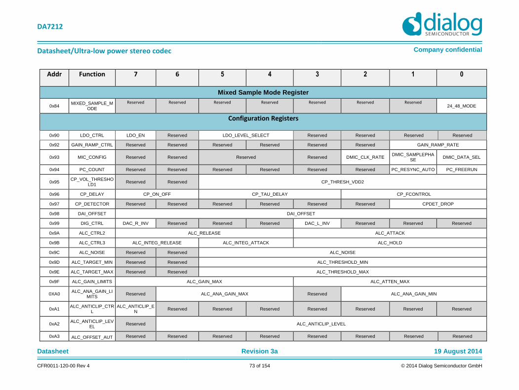
DA7212
Datasheet/Ultra-low power stereo codec Company confidential
Datasheet Revision 3a 19 August 2014
CFR0011-120-00 Rev 4 73 of 154 © 2014 Dialog Semiconductor GmbH
Addr Function 7 6 5 4 3 2 1 0
Mixed Sample Mode Register
0x84 MIXED_SAMPLE_M
ODE
Reserved Reserved Reserved Reserved Reserved Reserved Reserved 24_48_MODE
Configuration Registers
0x90 LDO_CTRL LDO_EN Reserved LDO_LEVEL_SELECT Reserved Reserved Reserved Reserved
0x92 GAIN_RAMP_CTRL Reserved Reserved Reserved Reserved Reserved Reserved GAIN_RAMP_RATE
0x93 MIC_CONFIG Reserved Reserved Reserved Reserved DMIC_CLK_RATE DMIC_SAMPLEPHA
SE DMIC_DATA_SEL
0x94 PC_COUNT Reserved Reserved Reserved Reserved Reserved Reserved PC_RESYNC_AUTO PC_FREERUN
0x95 CP_VOL_THRESHO
LD1 Reserved Reserved CP_THRESH_VDD2
0x96 CP_DELAY CP_ON_OFF CP_TAU_DELAY CP_FCONTROL
0x97 CP_DETECTOR Reserved Reserved Reserved Reserved Reserved Reserved CPDET_DROP
0x98 DAI_OFFSET DAI_OFFSET
0x99 DIG_CTRL DAC_R_INV Reserved Reserved Reserved DAC_L_INV Reserved Reserved Reserved
0x9A ALC_CTRL2 ALC_RELEASE ALC_ATTACK
0x9B ALC_CTRL3 ALC_INTEG_RELEASE ALC_INTEG_ATTACK ALC_HOLD
0x9C ALC_NOISE Reserved Reserved ALC_NOISE
0x9D ALC_TARGET_MIN Reserved Reserved ALC_THRESHOLD_MIN
0x9E ALC_TARGET_MAX Reserved Reserved ALC_THRESHOLD_MAX
0x9F ALC_GAIN_LIMITS ALC_GAIN_MAX ALC_ATTEN_MAX
0XA0 ALC_ANA_GAIN_LI
MITS Reserved ALC_ANA_GAIN_MAX Reserved ALC_ANA_GAIN_MIN
0xA1 ALC_ANTICLIP_CTR
L ALC_ANTICLIP_E
N Reserved Reserved Reserved Reserved Reserved Reserved Reserved
0xA2 ALC_ANTICLIP_LEV
EL Reserved ALC_ANTICLIP_LEVEL
0xA3 ALC_OFFSET_AUT Reserved Reserved Reserved Reserved Reserved Reserved Reserved Reserved

DA7212
Datasheet/Ultra-low power stereo codec Company confidential
Datasheet Revision 3a 19 August 2014
CFR0011-120-00 Rev 4 74 of 154 © 2014 Dialog Semiconductor GmbH
Addr Function 7 6 5 4 3 2 1 0
O_M_L
0xA4 ALC_OFFSET_AUT
O_U_L Reserved Reserved Reserved Reserved Reserved Reserved Reserved Reserved
0xA6 ALC_OFFSET_MAN
_M_L Reserved Reserved Reserved Reserved Reserved Reserved Reserved Reserved
0xA7 ALC_OFFSET_MAN
_U_L Reserved Reserved Reserved Reserved Reserved Reserved Reserved Reserved
0xA8 ALC_OFFSET_AUT
O_M_R Reserved Reserved Reserved Reserved Reserved Reserved Reserved Reserved
0xA9 ALC_OFFSET_AUT
O_U_R Reserved Reserved Reserved Reserved Reserved Reserved Reserved Reserved
0xAB ALC_OFFSET_MAN
_M_R Reserved Reserved Reserved Reserved Reserved Reserved Reserved Reserved
0xAC ALC_OFFSET_MAN
_U_R Reserved Reserved Reserved Reserved Reserved Reserved Reserved Reserved
0xAD ALC_CIC_OP_LVL_
CTRL Reserved Reserved Reserved Reserved Reserved Reserved Reserved Reserved
0xAE ALC_CIC_OP_LVL_
DATA Reserved Reserved Reserved Reserved Reserved Reserved Reserved Reserved
0xAF DAC_NG_SETUP_TI
ME Reserved Reserved Reserved Reserved
DAC_NG_RAMPDN_RATE
DAC_NG_RAMPUP_RATE
DAC_NG_SETUP_TIME
0xB0 DAC_NG_OFF_THR
ESHOLD Reserved Reserved Reserved Reserved Reserved DAC_NG_OFF_THRESHOLD
0xB1 DAC_NG_ON_THRE
SHOLD Reserved Reserved Reserved Reserved Reserved DAC_NG_ON_THRESHOLD
0xB2 DAC_NG_CTRL DAC_NG_EN Reserved Reserved Reserved Reserved Reserved Reserved Reserved
Tone Generation & Beep Registers
0xB4 TONE_GEN_CFG1 START_STOPN Reserved Reserved DTMF_EN DTMF_REG
0xB5 TONE_GEN_CFG2 GAIN Reserved Reserved SWG_SEL
0xB6 TONE_GEN_CYCLE
S Reserved Reserved Reserved Reserved Reserved BEEP_CYCLES

DA7212
Datasheet/Ultra-low power stereo codec Company confidential
Datasheet Revision 3a 19 August 2014
CFR0011-120-00 Rev 4 75 of 154 © 2014 Dialog Semiconductor GmbH
Addr Function 7 6 5 4 3 2 1 0
0xB7 TONE_GEN_FREQ1
_L FREQ1_L
0xB8 TONE_GEN_FREQ1
_U FREQ1_U
0xB9 TONE_GEN_FREQ2
_L FREQ2_L
0xBA TONE_GEN_FREQ2
_U FREQ2_U
0xBB TONE_GEN_ON_PE
R Reserved Reserved BEEP_ON_PER
0xBC TONE_GEN_OFF_P
ER Reserved Reserved BEEP_OFF_PER
System Controller Registers (2)
0xE0 SYSTEM_STATUS Reserved Reserved Reserved Reserved Reserved Reserved SC2_BUSY SC1_BUSY
0xFD SYSTEM_ACTIVE Reserved Reserved Reserved Reserved Reserved Reserved Reserved SYSTEM_ACTIVE

DA7212
Datasheet/Ultra-low power stereo codec Company confidential
Datasheet Revision 3a 19 August 2014
CFR0011-120-00 Rev 4 76 of 154 © 2014 Dialog Semiconductor GmbH
Status registers 15.2
Register
address Bit Type Label Default Description
0x02 STATUS1
7:0 R (reserved) 00000000
Register
address Bit Type Label Default Description
0x03 PLL_STATU
S
7:4 R (reserved) 0000
3 R PLL_BYPASS_A
CTIVE 0
Indicates whether the PLL is in bypass mode
0 = not in bypass mode
1 = bypass mode
2 R PLL_MCLK_STA
TUS 0
Indicates if the frequency on MCLK is greater than 1 MHz
0 = MCLK frequency 1 MHz or less
1 = MCLK frequency greater than 1 MHz
1 R PLL_SRM_LOCK 0
Asserted if the SRM is locked to the reference signal
0 = SRM not locked to reference signal
1 = SRM locked to reference signal
0 R PLL_LOCK 0
Asserted if the PLL is locked to the reference clock
0 = PLL not locked to reference clock
1 = PLL locked to reference clock

DA7212
Datasheet/Ultra-low power stereo codec Company confidential
Datasheet Revision 3a 19 August 2014
CFR0011-120-00 Rev 4 77 of 154 © 2014 Dialog Semiconductor GmbH
Register
address Bit Type Label Default Description
0x04 AUX_L_GAIN_STATUS
7:6 R (reserved) 00
5:0 R AUX_L_AMP_GAIN_STATUS
000000
Actual AUX_L amplifier gain
<010001 = -54 dB
010010 = -52.5 dB
010011 = -51 dB
continuing in +1.5 dB steps to
111110 = 13.5 dB
111111 = 15 dB
Register address
Bit Type Label Default Description
0x05 AUX_R_GAIN_STATUS
7:6 R (reserved) 00
5:0 R AUX_R_AMP_G
AIN_STATUS 000000
Actual AUX_R amplifier gain
<010001 = -54 dB
010010 = -52.5 dB
010011 = -51 dB
continuing in +1.5 dB steps to
111110 = 13.5 dB
111111 = 15 dB

DA7212
Datasheet/Ultra-low power stereo codec Company confidential
Datasheet Revision 3a 19 August 2014
CFR0011-120-00 Rev 4 78 of 154 © 2014 Dialog Semiconductor GmbH
Register
address Bit Type Label Default Description
0x06 MIC_1_GAIN_STATUS
7:3 R (reserved) 00000
2:0 R MIC_1_AMP_GA
IN_STATUS 001
Actual MIC_1 amplifier gain
000 = -6 dB
001 = 0 dB
010 = 6 dB
and continuing in +6 dB steps to
111 = 36 dB
Register
address Bit Type Label Default Description
0x07 MIC_2_GAIN_STATUS
7:3 R (reserved) 00000
2:0 R MIC_2_AMP_GA
IN_STATUS 001
Actual MIC_2 amplifier gain
000 = -6 dB
001 = 0 dB
010 = 6 dB
and continuing in +6 dB steps to
111 = 36 dB

DA7212
Datasheet/Ultra-low power stereo codec Company confidential
Datasheet Revision 3a 19 August 2014
CFR0011-120-00 Rev 4 79 of 154 © 2014 Dialog Semiconductor GmbH
Register
address Bit Type Label Default Description
0x08 MIXIN_L_GAIN_STATUS
7:4 R (reserved) 0000
3:0 R MIXIN_L_AMP_GAIN_STATUS
0000
Actual IN_L amplifier gain
0000 = -4.5 dB
0001 = -3 dB
0010 = -1.5 dB
0011 = 0 dB
continuing in +1.5 dB steps to
1111 = 18 dB
Register
address Bit Type Label Default Description
0x09 MIXIN_R_GAIN_STATU
S
7:4 R (reserved) 0000
3:0 R MIXIN_R_AMP_GAIN_STATUS
0000
Actual IN_R amplifier gain
0000 = -4.5 dB
0001 = -3 dB
0010 = -1.5 dB
0011 = 0 dB
continuing in +1.5 dB steps to
1111 = 18 dB

DA7212
Datasheet/Ultra-low power stereo codec Company confidential
Datasheet Revision 3a 19 August 2014
CFR0011-120-00 Rev 4 80 of 154 © 2014 Dialog Semiconductor GmbH
Register
address Bit Type Label Default Description
0x0A ADC_L_GAIN_STATUS
7 R (reserved) 0
6:0 R ADC_L_DIGITAL_GAIN_STATUS
0000000
Actual ADC_L digital gain
0000000 = -83.25 dB
0000001 = -82.50 dB
0000010 = -81.75 dB
continuing in +0.75 dB steps to
1111110 = 11.25 dB
1111111 = 12 dB
Note: 1101111 = 0 dB
Register
address Bit Type Label Default Description
0x0B ADC_R_GAIN_STATUS
7 R (reserved) 0
6:0 R ADC_R_DIGITAL_GAIN_STATUS
0000000
Actual ADC_R digital gain
0000000 = -83.25 dB
0000001 = -82.50 dB
0000010 = -81.75 dB
continuing in +0.75 dB steps to
1111110 = 11.25 dB
1111111 = 12 dB
Note: 1101111 = 0 dB

DA7212
Datasheet/Ultra-low power stereo codec Company confidential
Datasheet Revision 3a 19 August 2014
CFR0011-120-00 Rev 4 81 of 154 © 2014 Dialog Semiconductor GmbH
Register
address Bit Type Label Default Description
0x0C DAC_L_GAIN_STATUS
7 R (reserved) 0
6:0 R DAC_L_DIGITAL_GAIN_STATUS
0000000
Actual DAC_L digital gain
0000000 to 0000111 = mute
0001000 = -77.25 dB
0001001 = -76.50 dB
0001010 = -75.75 dB
continuing in +0.75 dB steps to
1111110 = 11.25 dB
1111111 = 12.00 dB
Note: 1101111 = 0 dB
Register
address Bit Type Label Default Description
0x0D DAC_R_GAIN_STATUS
7 R (reserved) 0
6:0 R DAC_R_DIGITAL_GAIN_STATUS
0000000
Actual DAC_R digital gain
0000000 to 0000111 = mute
0001000 = -77.25 dB
0001001 = -76.50 dB
0001010 = -75.75 dB
continuing in +0.75 dB steps to
1111110 = 11.25 dB
1111111 = 12.00 dB
Note: 1101111 = 0 dB

DA7212
Datasheet/Ultra-low power stereo codec Company confidential
Datasheet Revision 3a 19 August 2014
CFR0011-120-00 Rev 4 82 of 154 © 2014 Dialog Semiconductor GmbH
Register
address Bit Type Label Default Description
0x0E HP_L_GAIN_STATUS
7:6 R (reserved) 00
5:0 R HP_L_AMP_GAI
N_STATUS 000000
Actual HP_L amplifier gain
000000 = -57 dB
000001 = -56 dB
000010 = -55 dB
continuing in +1 dB steps to
111110 = 5 dB
111111 = 6 dB
Note: 111001 = 0 dB
Register
address Bit Type Label Default Description
0x0F HP_R_GAIN
_STATUS
7:6 R (reserved) 00
5:0 R HP_R_AMP_GAI
N_STATUS 000000
Actual HP_R amplifier gain
000000 = -57 dB
000001 = -56 dB
000010 = -55 dB
continuing in +1 dB steps to
111110 = 5 dB
111111 = 6 dB
Note: 111001 = 0 dB

DA7212
Datasheet/Ultra-low power stereo codec Company confidential
Datasheet Revision 3a 19 August 2014
CFR0011-120-00 Rev 4 83 of 154 © 2014 Dialog Semiconductor GmbH
Register
address Bit Type Label Default Description
0x10 LINE_GAIN_
STATUS
7:6 R (reserved) 00
5:0 R LINE_AMP_GAI
N_STATUS 000000
Actual LINE amplifier gain
000000 = -48 dB
000001 = -47 dB
continuing in +1 dB steps to
111110 = 14 dB
111111 = 15 dB
Note: 110000 = 0 dB

DA7212
Datasheet/Ultra-low power stereo codec Company confidential
Datasheet Revision 3a 19 August 2014
CFR0011-120-00 Rev 4 84 of 154 © 2014 Dialog Semiconductor GmbH
System initialisation registers 15.3
Register
address Bit Type Label Default Description
0x1D CIF_CTRL
7 R/W CIF_REG_SOFT
_RESET 0
Software reset that returns all the registers back to the default. Writing to this bit causes all the registers to reset
6:1 R/W (reserved) 000000
0 R/W CIF_I2C_WRITE
_MODE 0
Mode of operation for the I2C interface
0 = Page Mode
1 = Repeat Mode
Note: Page Mode supports both Page Mode and Repeat Mode reads and writes. Repeat Mode only supports Repeat Mode reads and writes.
Register
address Bit Type Label Default Description
0x21 DIG_ROUTI
NG_DAI
7:6 R/W (reserved) 00
5:4 R/W DAI_R_SRC 01
Data select for the DAI right output stream
00 = ADC left
01 = ADC right
10 = DAI input left data
11 = DAI input right data
3:2 R/W (reserved) 00
1:0 R/W DAI_L_SRC 00
Data select for the DAI left output stream
00 = ADC left
01 = ADC right
10 = DAI input left data
11 = DAI input right data

DA7212
Datasheet/Ultra-low power stereo codec Company confidential
Datasheet Revision 3a 19 August 2014
CFR0011-120-00 Rev 4 85 of 154 © 2014 Dialog Semiconductor GmbH
Register
address Bit Type Label Default Description
0x22 SR
7:4 R/W (reserved) 0000
3:0 R/W SR 1010
Sample rate control
0001 = 8 kHz
0010 = 11.025 kHz
0011 = 12 kHz
0100 = reserved
0101 = 16 kHz
0110 = 22 kHz
0111 = 24 kHz
1000 = reserved
1001 = 32 kHz
1010 = 44.1 kHz (Note 37)
1011 = 48 kHz
1110 = 88.2 kHz
1111 = 96 kHz
Note 37 b1011 (48kHz) is the only valid setting when using 24-48 mode (24_48_MODE = 1)
Register
address Bit Type Label Default Description
0x23 REFERENC
ES
7 R/W (reserved) 1
6 R/W (reserved) 0
5 R/W VMID_FAST_DIS
CHARGE 0
VMID fast discharge enable:
0 = low noise slow discharge mode
1 = high noise fast discharge mode
4 R/W VMID_FAST_CH
ARGE 0
VMID fast charge enable:
0 = low noise slow charge mode
1 = high noise fast charge mode
3 R/W BIAS_EN 0
Master bias enable:
0 = disabled
1 = enabled
2 R/W (reserved) 0
1:0 R/W (reserved) 00

DA7212
Datasheet/Ultra-low power stereo codec Company confidential
Datasheet Revision 3a 19 August 2014
CFR0011-120-00 Rev 4 86 of 154 © 2014 Dialog Semiconductor GmbH
Register
address Bit Type Label Default Description
0x24 PLL_FRAC_
TOP
7:5 R/W (reserved) 000
4:0 R/W PLL_FBDIV_FRA
C_TOP 00000
PLL fractional division value (top bits). The full PLL fractional division value is a concatenation of these bits (MSB) and PLL_FBDIV_FRAC_BOT (LSB)
Register
address Bit Type Label Default Description
0x25 PLL_FRAC_
BOT 7:0 R/W
PLL_FBDIV_FRAC_BOT
00000000
PLL fractional division value (bottom bits). The full PLL fractional division value is a concatenation of PLL_FBDIV_FRAC_TOP (MSB) and these bits (LSB)
Register
address Bit Type Label Default Description
0x26 PLL_INTEG
ER
7 R/W (reserved) 0
6:0 R/W PLL_FBDIV_INT
EGER 0100000 PLL integer division value
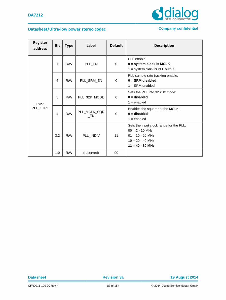
DA7212
Datasheet/Ultra-low power stereo codec Company confidential
Datasheet Revision 3a 19 August 2014
CFR0011-120-00 Rev 4 87 of 154 © 2014 Dialog Semiconductor GmbH
Register
address Bit Type Label Default Description
0x27 PLL_CTRL
7 R/W PLL_EN 0
PLL enable:
0 = system clock is MCLK
1 = system clock is PLL output
6 R/W PLL_SRM_EN 0
PLL sample rate tracking enable:
0 = SRM disabled
1 = SRM enabled
5 R/W PLL_32K_MODE 0
Sets the PLL into 32 kHz mode:
0 = disabled
1 = enabled
4 R/W PLL_MCLK_SQR
_EN 0
Enables the squarer at the MCLK:
0 = disabled
1 = enabled
3:2 R/W PLL_INDIV 11
Sets the input clock range for the PLL:
00 = 2 - 10 MHz
01 = 10 - 20 MHz
10 = 20 - 40 MHz
11 = 40 - 80 MHz
1:0 R/W (reserved) 00

DA7212
Datasheet/Ultra-low power stereo codec Company confidential
Datasheet Revision 3a 19 August 2014
CFR0011-120-00 Rev 4 88 of 154 © 2014 Dialog Semiconductor GmbH
Register
address Bit Type Label Default Description
0x28 DAI_CLK_M
ODE
7 R/W DAI_CLK_EN 0
DAI master mode enable:
0 = slave mode (BCLK/WCLK inputs)
1 = master mode (BCLK/WCLK outputs)
6:4 R/W (reserved) 000
3 R/W DAI_WCLK_POL 0
DAI word clock polarity:
0 = normal polarity
1 = inverted polarity
2 R/W DAI_CLK_POL 0 DAI bit clock polarity: 0 = normal
1 = inverted
1:0 R/W DAI_BCLKS_PE
R_WCLK 01
DAI master mode BCLK number per WCLK period: 00 = BCLK = 32 01 = BCLK = 64
10 = BCLK = 128 11 = BCLK = 256

DA7212
Datasheet/Ultra-low power stereo codec Company confidential
Datasheet Revision 3a 19 August 2014
CFR0011-120-00 Rev 4 89 of 154 © 2014 Dialog Semiconductor GmbH
Register
address Bit Type Label Default Description
0x29 DAI_CTRL
7 R/W DAI_EN 0 DAI enable: 0 = disabled 1 = enabled
6 R/W DAI_OE 0 DAI output enable: 0 = DATOUT pin is high impedence 1 = DATOUT pin is driven when required
5 R/W DAI_TDM_MOD
E_EN 0
DAI TDM mode enable: 0 = DAI normal mode 1 = DAI TDM mode
4 R/W DAI_MONO_MO
DE_EN 0
DAI mono mode enable: 0 = DAI stereo mode 1 = DAI mono mode
Note: DAI mono mode can only be enabled when the DSP data format = DSP Mode (DAI_FORMAT = 11)
3:2 R/W DAI_WORD_LE
NGTH 10
DAI data word length: 00 = 16 bits per channel 01 = 20 bits per channel 10 = 24 bits per channel 11 = 32 bits per channel
1:0 R/W DAI_FORMAT 00
DAI data format: 00 = I2S mode 01 = left justified mode 10 = right justified mode 11 = DSP mode

DA7212
Datasheet/Ultra-low power stereo codec Company confidential
Datasheet Revision 3a 19 August 2014
CFR0011-120-00 Rev 4 90 of 154 © 2014 Dialog Semiconductor GmbH
Register
address Bit Type Label Default Description
0x2A DIG_ROUTI
NG_DAC
7 R/W DAC_R_MONO 0
When asserted, the DAI right input stream is replaced with a mono mix of left and right
0 = Right input stream
1 = Mono mix of left and right input streams
6 R/W (reserved) 0
5:4 R/W DAC_R_SRC 11
Data select to the DAC_R path: 00 = ADC left output 01 = ADC right output 10 = Determined by DAC_L_MONO (bit [3] of this register) 11 = Determined by DAC_R_MONO (bit [7] of this register)
Note: The beep generator is omited from the signal path if this is set to ‘00’ or ‘01’
3 R/W DAC_L_MONO 0
When asserted, the DAI left input stream is replaced with a mono mix of left and right
0 = Left input stream
1 = Mono mix of left and right input streams
2 R/W (reserved) 0
1:0 R/W DAC_L_SRC 10
Data select to the DAC_L path: 00 = ADC left output 01 = ADC right output 10 = Determined by DAC_L_MONO (bit [3] of this register)
11 = Determined by DAC_R_MONO (bit [7] of this register)
Note: The beep generator is omited from the signal path if this is set to ‘00’ or ‘01’

DA7212
Datasheet/Ultra-low power stereo codec Company confidential
Datasheet Revision 3a 19 August 2014
CFR0011-120-00 Rev 4 91 of 154 © 2014 Dialog Semiconductor GmbH
Register
address Bit Type Label Default Description
0x2B ALC_CTRL1
7 R/W ALC_R_EN 0
Enables the ALC operation on the right ADC channel:
0 = disabled
1 = enabled
6 R/W (reserved) 0
5 R ALC_CALIB_OV
ERFLOW 0
Offset overflow during calibration
0 = no offset overflow
1 = offset overflow
4 R/W ALC_AUTO_CAL
IB_EN 0
Automatic calibration enable (self clearing bit)
0 = disabled
1 = enabled
3 R/W ALC_L_EN 0
Enables the ALC operation on the left ADC channel:
0 = disabled
1 = enabled
2 R/W ALC_CALIB_MO
DE 0
Calibration mode 0 = Automatic calibration
1 = Manual calibration
1 R/W ALC_SYNC_MO
DE 0
Selects the ALC Operation Mode:
0 = Full digital gain solution
1 = Mixed digital/analogue gain solution
0 R/W ALC_OFFSET_E
N 0
Enable DC Offset cancellation:
0 = disabled
1 = enabled

DA7212
Datasheet/Ultra-low power stereo codec Company confidential
Datasheet Revision 3a 19 August 2014
CFR0011-120-00 Rev 4 92 of 154 © 2014 Dialog Semiconductor GmbH
Input gain/select filter registers 15.4
Register address
Bit Type Label Default Description
0x30 AUX_L_GAI
N
7:6 R/W (reserved) 00
5:0 R/W AUX_L_AMP_G
AIN 110101
Gain setting for the AUX left amplifier (1.5 dB step):
<010001 = -54 dB
010010 = -52.5 dB
010011 = -51 dB
continuing in +1.5 dB steps to
111110 = 13.5 dB
111111 = 15 dB
Note: 110101 = 0 dB (default)
Register address
Bit Type Label Default Description
0x31 AUX_R_GAI
N
7:6 R/W (reserved) 00
5:0 R/W AUX_R_AMP_G
AIN 110101
Gain setting for the AUX right amplifier (1.5 dB step):
<010001 = -54 dB
010010 = -52.5 dB
010011 = -51 dB
continuing in +1.5 dB steps to
111110 = 13.5 dB
111111 = 15 dB
Note: 110101 = 0 dB (default)

DA7212
Datasheet/Ultra-low power stereo codec Company confidential
Datasheet Revision 3a 19 August 2014
CFR0011-120-00 Rev 4 93 of 154 © 2014 Dialog Semiconductor GmbH
Register address
Bit Type Label Default Description
0x32 MIXIN_L_SE
LECT
7 R/W DMIC_L_EN 0
Enable the left DMIC input:
0 = disabled
1 = enabled
6 R/W (reserved) 0
5:4 R/W (reserved) 00
3 R/W MIXIN_R 0 0 = MIXIN_R not mixed in
1 = MIXIN_R mixed in
2 R/W MIC2_SEL 0 0 = MIC2 input not mixed in
1 = MIC2 input mixed in
1 R/W MIC1_SEL 0 0 = MIC1 input not mixed in
1 = MIC1 input mixed in
0 R/W AUX_L_SEL 0 0 = AUX_L input not mixed in
1 = AUX_L input mixed in
Register address
Bit Type Label Default Description
0x33 MIXIN_R_S
ELECT
7 R/W DMIC_R_EN 0
Enable the right DMIC input:
0 = disabled
1 = enabled
6 R/W (reserved) 0
5:4 R/W (reserved) 00
3 R/W MIXIN_L_SEL 0 0 = MIXIN_L input not mixed in
1 = MIXIN_L input mixed in
2 R/W MIC1_SEL 0 0 = MIC_1 input not mixed in
1 = MIC_1 input mixed in
1 R/W MIC2_SEL
0 0 = MIC_2 input not mixed in
1 = MIC_2 input mixed in
0 R/W AUX_R_SEL 0 0 = AUX_R input not mixed in
1 = AUX_R input mixed in

DA7212
Datasheet/Ultra-low power stereo codec Company confidential
Datasheet Revision 3a 19 August 2014
CFR0011-120-00 Rev 4 94 of 154 © 2014 Dialog Semiconductor GmbH
Register address
Bit Type Label Default Description
0x34 MIXIN_L_GA
IN
7:4 R/W (reserved) 0000
3:0 R/W MIXIN_L_AMP_
GAIN 0011
Gain setting for the IN left amplifier (1.5 dB step):
0000 = -4.5 dB
0001 = -3 dB
0010 = -1.5 dB
0011 = 0 dB
continuing in +1.5 dB steps to
1111 = 18 dB
Register address
Bit Type Label Default Description
0x35 MIXIN_R_G
AIN
7:4 R/W (reserved) 0000
3:0 R/W MIXIN_R_AMP_
GAIN 0011
Gain setting for the IN right amplifier (1.5 dB step):
0000 = -4.5 dB
0001 = -3 dB
0010 = -1.5 dB
0011 = 0 dB
continuing in +1.5 dB steps to
1111 = 18 dB

DA7212
Datasheet/Ultra-low power stereo codec Company confidential
Datasheet Revision 3a 19 August 2014
CFR0011-120-00 Rev 4 95 of 154 © 2014 Dialog Semiconductor GmbH
Register address
Bit Type Label Default Description
0x36 ADC_L_GAI
N
7 R/W (reserved) 0
6:0 R/W ADC_L_DIGITAL
_GAIN 1101111
ADC left digital gain (0.75 dB step):
0000000 = -83.25 dB
0000001 = -82.50 dB
0000010 = -81.75 dB
continuing in +0.75 dB steps to
1111110 = 11.25 dB
1111111 = 12 dB
Note: 1101111 = 0 dB (default)
Register address
Bit Type Label Default Description
0x37 ADC_R_GAI
N
7 R/W (reserved) 0
6:0 R/W ADC_R_DIGITAL
_GAIN 1101111
ADC right digital gain (0.75 dB step):
0000000 = -83.25 dB
0000001 = -82.50 dB
0000010 = -81.75 dB
continuing in +0.75 dB steps to
1111110 = 11.25 dB
1111111 = 12 dB
Note: 1101111 = 0 dB (default)

DA7212
Datasheet/Ultra-low power stereo codec Company confidential
Datasheet Revision 3a 19 August 2014
CFR0011-120-00 Rev 4 96 of 154 © 2014 Dialog Semiconductor GmbH
Register address
Bit Type Label Default Description
0x38 ADC_FILTE
RS1
7 R/W ADC_HPF_EN 1
ADC high pass filter enable:
0 = disabled
1 = enabled
6 R/W (reserved) 0
5:4 R/W ADC_AUDIO_HP
F_CORNER 00
Cut-off frequency at the 3 dB for the High Pass Filter at 48 kHz (for other frequencies see Table 30):
00 = 2 Hz
01 = 4 Hz
10 = 8 Hz
11 = 16 Hz
3 R/W ADC_VOICE_EN 0
ADC voice filter enable:
0 = disabled
1 = enabled
2:0 R/W ADC_VOICE_HPF_CORNER
000
Cutoff frequency at the 3 dB for the Voice Filter at 8 kHz (for other frequencies see Table 31):
000 = 2.5 Hz
001 = 25 Hz,
010 = 50 Hz
011 = 100 Hz
100 = 150 Hz
101 = 200 Hz
110 = 300 Hz
111 = 400 Hz

DA7212
Datasheet/Ultra-low power stereo codec Company confidential
Datasheet Revision 3a 19 August 2014
CFR0011-120-00 Rev 4 97 of 154 © 2014 Dialog Semiconductor GmbH
Register address
Bit Type Label Default Description
0x39 MIC_1_GAI
N
7:3 R/W (reserved) 00000
2:0 R/W MIC_1_AMP_GA
IN 001
Gain setting for the MIC left amplifier (6 dB step):
000 = -6 dB
001 = 0 dB
010 = 6 dB
continuing in 6 dB steps to
111 = 36 dB
Note: This setting is ignored if the ALC is enabled (ALC_R_EN or ALC_L_EN= 1) and the ALC is running in Syncronised Mode (ALC_SYNC_MODE = 1)
Register address
Bit Type Label Default Description
0x3A MIC_2_GAI
N
7:3 R/W (reserved) 00000
2:0 R/W MIC_2_AMP_GA
IN 001
Gain setting for the MIC right amplifier (6 dB step):
000 = -6 dB
001 = 0 dB
010 = 6 dB
continuing in 6 dB steps to
111 = 36 dB
Note: This setting is ignored if the ALC is enabled (ALC_R_EN or ALC_L_EN= 1) and the ALC is running in Syncronised Mode (ALC_SYNC_MODE = 1)

DA7212
Datasheet/Ultra-low power stereo codec Company confidential
Datasheet Revision 3a 19 August 2014
CFR0011-120-00 Rev 4 98 of 154 © 2014 Dialog Semiconductor GmbH
Output Gain-Filter Registers 15.4.1
Register address
Bit Type Label Default Description
0x40 DAC_FILTE
RS5
7 R/W DAC_SOFTMUT
E_EN 0
DAC soft mute enable on both channels:
0 = disabled
1 = enabled
6:4 R/W DAC_SOFTMUT
E_RATE 000
Softmute gain update rate (samples per 0.1875 dB):
000 = 1
001 = 2
010 = 4
011 = 8
100 = 16
101 = 32
110 = 64
111 = reserved
3:0 R/W (reserved) 0000

DA7212
Datasheet/Ultra-low power stereo codec Company confidential
Datasheet Revision 3a 19 August 2014
CFR0011-120-00 Rev 4 99 of 154 © 2014 Dialog Semiconductor GmbH
Register address
Bit Type Label Default Description
0x41 DAC_FILTE
RS2
7:4 R/W DAC_EQ_BAND
2 1000
Gain setting for the DAC 5-Band EQ band 2 (1.5 dB steps).
0000 = -10.5 dB
0001 = -9 dB
continuing in +1.5 dB steps to
1110 = 10.5 dB
1111 = 12 dB
Note: 0111 = 0 dB
Note: 1000 = 1.5 dB (default)
3:0 R/W DAC_EQ_BAND
1 1000
Gain setting for the DAC 5-Band EQ band 1 (1.5 dB steps):
0000 = -10.5 dB
0001 = -9 dB
continuing in +1.5 dB steps to
1110 = 10.5 dB
1111 = 12 dB
Note: 0111 = 0 dB
Note: 1000 = 1.5 dB (default)

DA7212
Datasheet/Ultra-low power stereo codec Company confidential
Datasheet Revision 3a 19 August 2014
CFR0011-120-00 Rev 4 100 of 154 © 2014 Dialog Semiconductor GmbH
Register address
Bit Type Label Default Description
0x42 DAC_FILTE
RS3
7:4 R/W DAC_EQ_BAND
4 1000
Gain setting for the DAC 5-Band EQ band 4 (1.5 dB steps).
0000 = -10.5 dB
0001 = -9 dB
continuing in +1.5 dB steps to
1110 = 10.5 dB
1111 = 12 dB
Note: 0111 = 0 dB
Note: 1000 = 1.5 dB (default)
3:0 R/W DAC_EQ_BAND
3 1000
Gain setting for the DAC 5-Band EQ band 3 (1.5 dB steps):
0000 = -10.5 dB
0001 = -9 dB
continuing in +1.5 dB steps to
1110 = 10.5 dB
1111 = 12 dB
Note: 0111 = 0 dB
Note: 1000 = 1.5 dB (default)

DA7212
Datasheet/Ultra-low power stereo codec Company confidential
Datasheet Revision 3a 19 August 2014
CFR0011-120-00 Rev 4 101 of 154 © 2014 Dialog Semiconductor GmbH
Register address
Bit Type Label Default Description
0x43 DAC_FILTE
RS4
7 R/W DAC_EQ_EN 0
DAC 5-band equaliser enable:
0 = disabled
1 = enabled
6:4 R/W (reserved) 000
3:0 R/W DAC_EQ_BAND
5 1000
Gain setting for the DAC 5-Band EQ band 5 (1.5 dB steps):
0000 = -10.5 dB
0001 = -9 dB
continuing in +1.5 dB steps to
1110 = 10.5 dB
1111 = 12 dB
Note: 0111 = 0 dB
Note: 1000 = 1.5 dB (default)

DA7212
Datasheet/Ultra-low power stereo codec Company confidential
Datasheet Revision 3a 19 August 2014
CFR0011-120-00 Rev 4 102 of 154 © 2014 Dialog Semiconductor GmbH
Register address
Bit Type Label Default Description
0x44 DAC_FILTE
RS1
7 R/W DAC_HPF_EN 1
DAC High Pass filter enable:
0 = disabled
1 = enabled
6 R/W (reserved) 0
5:4 R/W DAC_AUDIO_HP
F_CORNER 00
Cutoff frequency at the 3 dB for the High Pass Filter at 48 kHz (for other frequencies see Table 30):
00 = 2 Hz
01 = 4 Hz
10 = 8 Hz
11 = 16 Hz
3 R/W DAC_VOICE_EN 0
DAC voice filter enable:
0 = disabled
1 = enabled
2:0 R/W DAC_VOICE_HP
F_CORNER 000
Cutoff frequency at the 3 dB for the Voice Filter at 8 kHz (for other frequencies see Table 31):
000 = 2.5 Hz
001 = 25 Hz
010 = 50 Hz
011 = 100 Hz
100 = 150 Hz
101 = 200 Hz
110 = 300 Hz
111 = 400 Hz
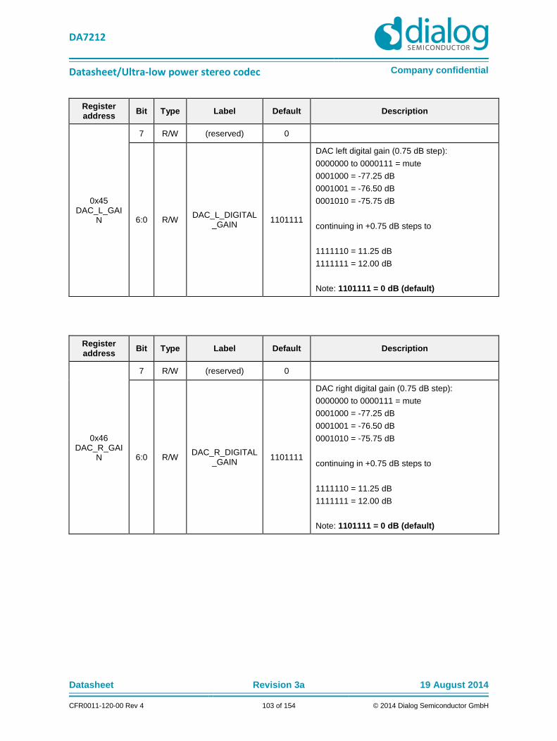
DA7212
Datasheet/Ultra-low power stereo codec Company confidential
Datasheet Revision 3a 19 August 2014
CFR0011-120-00 Rev 4 103 of 154 © 2014 Dialog Semiconductor GmbH
Register address
Bit Type Label Default Description
0x45 DAC_L_GAI
N
7 R/W (reserved) 0
6:0 R/W DAC_L_DIGITAL
_GAIN 1101111
DAC left digital gain (0.75 dB step):
0000000 to 0000111 = mute
0001000 = -77.25 dB
0001001 = -76.50 dB
0001010 = -75.75 dB
continuing in +0.75 dB steps to
1111110 = 11.25 dB
1111111 = 12.00 dB
Note: 1101111 = 0 dB (default)
Register address
Bit Type Label Default Description
0x46 DAC_R_GAI
N
7 R/W (reserved) 0
6:0 R/W DAC_R_DIGITAL
_GAIN 1101111
DAC right digital gain (0.75 dB step):
0000000 to 0000111 = mute
0001000 = -77.25 dB
0001001 = -76.50 dB
0001010 = -75.75 dB
continuing in +0.75 dB steps to
1111110 = 11.25 dB
1111111 = 12.00 dB
Note: 1101111 = 0 dB (default)

DA7212
Datasheet/Ultra-low power stereo codec Company confidential
Datasheet Revision 3a 19 August 2014
CFR0011-120-00 Rev 4 104 of 154 © 2014 Dialog Semiconductor GmbH
Register address
Bit Type Label Default Description
0x47 CP_CTRL
7 R/W CP_EN 0
Charge pump enable:
0 = disabled
1 = enabled
6 R/W CP_SMALL_SWITCH_FREQ_EN
1
Charge pump low-load low-power mode enable:
0 = disabled
1 = enabled
5:4 R/W CP_MCHANGE 10
Charge pump tracking mode select:
00 = voltage level is controlled by CP_MOD
01 = voltage level is controlled by the output PGA gain setting
10 = voltage level is controlled by the DAC signal level
11 = voltage level is controlled by the output signal magnitude
3:2 R/W CP_MOD 00
Charge pump manual mode level control:
00 = standby
01 = reserved
10 = CPVDD/2
11 = CPVDD/1
1:0 R/W CP_ANALOGUE
_LVL 01
Charge pump analogue feedback control mode:
00 = no feedback
01 = low voltage indicator boosts charge pump
10 = low voltage indicator restarts charge pump cycle
11 = Reserved

DA7212
Datasheet/Ultra-low power stereo codec Company confidential
Datasheet Revision 3a 19 August 2014
CFR0011-120-00 Rev 4 105 of 154 © 2014 Dialog Semiconductor GmbH
Register address
Bit Type Label Default Description
0x48 HP_L_GAIN
7:6 R/W (reserved) 00
5:0 R/W HP_L_AMP_GAI
N 111001
Headphone left amplifier gain (1 dB step):
000000 = -57 dB
000001 = -56 dB
000010 = -55 dB
continuing in +1 dB steps to
111110 = 5 dB
111111 = 6 dB
Note: 111001 = 0 dB (default)
Register address
Bit Type Label Default Description
0x49 HP_R_GAIN
7:6 R/W (reserved) 00
5:0 R/W HP_R_AMP_GAI
N 111001
Headphone right amplifier gain (1 dB step):
000000 = -57 dB
000001 = -56 dB
000010 = -55 dB
continuing in +1 dB steps to
111110 = 5 dB
111111 = 6 dB
Note: 111001 = 0 dB (default)
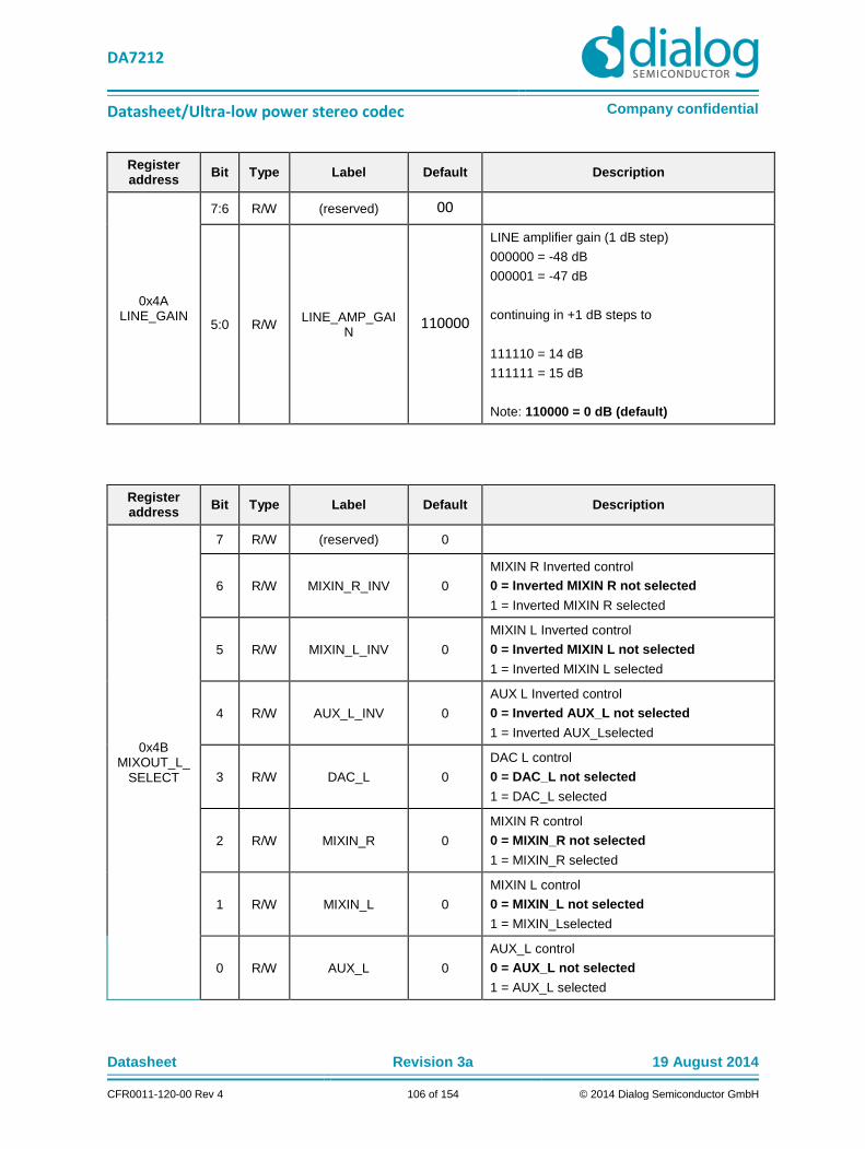
DA7212
Datasheet/Ultra-low power stereo codec Company confidential
Datasheet Revision 3a 19 August 2014
CFR0011-120-00 Rev 4 106 of 154 © 2014 Dialog Semiconductor GmbH
Register address
Bit Type Label Default Description
0x4A LINE_GAIN
7:6 R/W (reserved) 00
5:0 R/W LINE_AMP_GAI
N 110000
LINE amplifier gain (1 dB step)
000000 = -48 dB
000001 = -47 dB
continuing in +1 dB steps to
111110 = 14 dB
111111 = 15 dB
Note: 110000 = 0 dB (default)
Register address
Bit Type Label Default Description
0x4B MIXOUT_L_
SELECT
7 R/W (reserved) 0
6 R/W MIXIN_R_INV 0
MIXIN R Inverted control
0 = Inverted MIXIN R not selected
1 = Inverted MIXIN R selected
5 R/W MIXIN_L_INV 0
MIXIN L Inverted control
0 = Inverted MIXIN L not selected
1 = Inverted MIXIN L selected
4 R/W AUX_L_INV 0
AUX L Inverted control
0 = Inverted AUX_L not selected
1 = Inverted AUX_Lselected
3 R/W DAC_L 0
DAC L control
0 = DAC_L not selected
1 = DAC_L selected
2 R/W MIXIN_R 0
MIXIN R control
0 = MIXIN_R not selected
1 = MIXIN_R selected
1 R/W MIXIN_L 0
MIXIN L control
0 = MIXIN_L not selected
1 = MIXIN_Lselected
0 R/W AUX_L 0
AUX_L control
0 = AUX_L not selected
1 = AUX_L selected

DA7212
Datasheet/Ultra-low power stereo codec Company confidential
Datasheet Revision 3a 19 August 2014
CFR0011-120-00 Rev 4 107 of 154 © 2014 Dialog Semiconductor GmbH
Register address
Bit Type Label Default Description
0x4C MIXOUT_R_
SELECT
7 R/W (reserved) 0
6 R/W MIXIN_L_INV 0
MIXIN L Inverted control
0 = Inverted MIXIN L not selected
1 = Inverted MIXIN L selected
5 R/W MIXIN_R_INV 0
MIXIN R Inverted control
0 = Inverted MIXIN R not selected
1 = Inverted MIXIN R selected
4 R/W AUX_R_INV 0
AUX R Inverted control
0 = Inverted AUX_R not selected
1 = Inverted AUX_R selected
3 R/W DAC_R 0
DAC R control
0 = DAC_R not selected
1 = DAC_R selected
2 R/W MIXIN_L 0
MIXIN L control
0 = MIXIN_L not selected
1 = MIXIN_L selected
1 R/W MIXIN_R 0
MIXIN R control
0 = MIXIN_R not selected
1 = MIXIN_R selected
0 R/W AUX_R 0
AUX_R control
0 = AUX_R not selected
1 = AUX_R selected
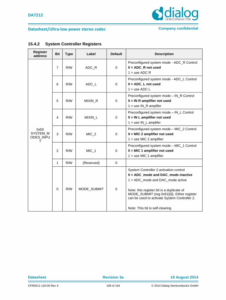
DA7212
Datasheet/Ultra-low power stereo codec Company confidential
Datasheet Revision 3a 19 August 2014
CFR0011-120-00 Rev 4 108 of 154 © 2014 Dialog Semiconductor GmbH
System Controller Registers 15.4.2
Register address
Bit Type Label Default Description
0x50 SYSTEM_MODES_INPU
T
7 R/W ADC_R 0
Preconfigured system mode - ADC_R Control
0 = ADC_R not used
1 = use ADC R
6 R/W ADC_L 0
Preconfigured system mode - ADC_L Control
0 = ADC_L not used
1 = use ADC L
5 R/W MIXIN_R 0
Preconfigured system mode – IN_R Control
0 = IN R amplifier not used
1 = use IN_R amplifer
4 R/W MIXIN_L 0
Preconfigured system mode – IN_L Control
0 = IN L amplifier not used
1 = use IN_L amplifer
3 R/W MIC_2 0
Preconfigured system mode – MIC_2 Control
0 = MIC 2 amplifier not used
1 = use MIC 2 amplifier
2 R/W MIC_1 0
Preconfigured system mode – MIC_1 Control
0 = MIC 1 amplifier not used
1 = use MIC 1 amplifier
1 R/W (Reserved) 0
0 R/W MODE_SUBMIT 0
System Controller 2 activation control
0 = ADC_mode and DAC_mode inactive
1 = ADC_mode and DAC_mode active
Note: this register bit is a duplicate of MODE_SUBMIT (reg 0x51[0]). Either register can be used to activate System Controller 2.
Note: This bit is self-clearing.

DA7212
Datasheet/Ultra-low power stereo codec Company confidential
Datasheet Revision 3a 19 August 2014
CFR0011-120-00 Rev 4 109 of 154 © 2014 Dialog Semiconductor GmbH
Register address
Bit Type Label Default Description
0x51 SYSTEM_MODES_OUT
PUT
7:3 R/W DAC_R 0
Preconfigured system mode – DAC_R Control
0 = DAC_R not used
1 = use DAC R
6 R/W DAC_L 0
Preconfigured system mode – DAC_L Control
0 = DAC_L not used
1 = use DAC L
5 R/W HP_R 0
Preconfigured system mode – HP_R Control
0 = HP_R not used
1 = use HP_R amplifier
4 R/W HP_L 0
Preconfigured system mode – HP_L Control
0 = HP_L not used
1 = use HP_L amplifier
3 R/W LINE 0
Preconfigured system mode – LINE Control
0 = LINE not used
1 = use LINE amplifier
2 R/W AUX_R 0
Preconfigured system mode – AUX_R Control
0 = AUX_R amplifer not used
1 = use AUX_R amplifier
1 R/W AUX_L 0
Preconfigured system mode – AUX_L Control
0 = AUX_L amplifier not used
1 = use AUX_L amplifier
0 R/W MODE_SUBMIT 0
System Controller 2 activation control
0 = ADC_mode and DAC_mode inactive
1 = ADC_mode and DAC_mode active
Note: this register bit is a duplicate of MODE_SUBMIT (reg 0x51[0]). Either register can be used to activate System Controller 2.
Note: This bit is self-clearing.

DA7212
Datasheet/Ultra-low power stereo codec Company confidential
Datasheet Revision 3a 19 August 2014
CFR0011-120-00 Rev 4 110 of 154 © 2014 Dialog Semiconductor GmbH
Control Registers 15.4.3
Register address
Bit Type Label Default Description
0x60 AUX_L_CTR
L
7 R/W AUX_L_AMP_EN 0
AUX_L amplifier enable:
0 = disabled
1 = enabled
6 R/W AUX_L_AMP_M
UTE_EN 1
AUX_L amplifier mute enable:
0 = disabled
1 = enabled
5 R/W AUX_L_AMP_RA
MP_EN 0
AUX_L amplifier gain ramping enable (overrides zero crossing):
0 = disabled
1 = enabled
4 R/W AUX_L_AMP_ZC
_EN 0
AUX_L amplifier zero cross gain update mode enable:
0 = disabled
1 = enabled
3:2 R/W AUX_L_AMP_ZC
_SEL 01
Selects where the zero cross detection on the AUX_L input is measured:
00 = Input of AUX_L amplifier
01 = input of AUX_L amplifier if gain 4.5 dB otherwise on the output
10 = Neither (no zero cross possible)
11 = Output of AUX_L amplifier
1:0 R/W (reserved) 00

DA7212
Datasheet/Ultra-low power stereo codec Company confidential
Datasheet Revision 3a 19 August 2014
CFR0011-120-00 Rev 4 111 of 154 © 2014 Dialog Semiconductor GmbH
Register address
Bit Type Label Default Description
0x61 AUX_R_CT
RL
7 R/W AUX_R_AMP_E
N 0
AUX_R amplifier enable:
0 = disabled
1 = enabled
6 R/W AUX_R_AMP_M
UTE_EN 1
AUX_R amplifier mute enable:
0 = disabled
1 = enabled
5 R/W AUX_R_AMP_R
AMP_EN 0
AUX_R amplifier gain ramping enable (overrides zero crossing):
0 = disabled
1 = enabled
4 R/W AUX_R_AMP_Z
C_EN 0
AUX_R amplifier zero cross gain update mode enable:
0 = disabled
1 = enabled
3:2 R/W AUX_R_AMP_Z
C_SEL 01
Selects where the zero cross detection on the AUX_R input is measured:
00 = Input of AUX_R amplifier
01 = input of AUX_R amplifier if gain 4.5 dB otherwise on the output
10 = Neither (no zero cross possible)
11 = Output of AUX_R amplifier
1:0 R/W (reserved) 00

DA7212
Datasheet/Ultra-low power stereo codec Company confidential
Datasheet Revision 3a 19 August 2014
CFR0011-120-00 Rev 4 112 of 154 © 2014 Dialog Semiconductor GmbH
Register address
Bit Type Label Default Description
0x62 MICBIAS_C
TRL
7 R/W MICBIAS2_EN 0
Microphone 2 bias enable:
0 = Disable
1 = Enable
6 R/W (reserved) 0
5:4 R/W MICBIAS2_LEVE
L 01
Microphone 2 bias level
00 = 1.6 V
01 = 2.2 V
10 = 2.5 V
11 = 3.0 V
3 R/W MICBIAS1_EN 0
Microphone 1 bias enable:
0 = Disable
1 = Enable
2 R/W (reserved) 0
1:0 R/W MICBIAS1_LEVE
L 01
Microphone 1 bias level
00 = 1.6 V
01 = 2.2 V
10 = 2.5 V
11 = 3.0 V

DA7212
Datasheet/Ultra-low power stereo codec Company confidential
Datasheet Revision 3a 19 August 2014
CFR0011-120-00 Rev 4 113 of 154 © 2014 Dialog Semiconductor GmbH
Register address
Bit Type Label Default Description
0x63 MIC_1_CTR
L
7 R/W MIC_1_AMP_EN 0
MIC_1 amplifier enable:
0 = disabled
1 = enabled
6 R/W MIC_1_AMP_MU
TE_EN 1
MIC_1 amplifier mute enable:
0 = amplifier unmuted
1 = amplifier muted
5 R/W (reserved) 0
4 R/W (reserved) 0
3:2 R/W MIC_1_AMP_IN_
SEL 00
MIC_1 input source select: 00 = differential
01 = MIC_1_P single-ended 10 = MIC_1_N single-ended 11 = reserved
1:0 R/W
(reserved) 00
Register address
Bit Type Label Default Description
0x64 MIC_2_CTR
L
7 R/W MIC_2_AMP_EN 0
MIC_2 amplifier enable:
0 = disabled
1 = enabled
6 R/W MIC_2_AMP_MU
TE_EN 1
MIC_2 amplifier mute enable:
0 = amplifier unmuted
1 = amplifier muted
5 R/W (reserved) 0
4 R/W (reserved) 0
3:2 R/W MIC_2_AMP_IN_
SEL 00
MIC_2 input source select: 00 = differential
01 = MIC_2_P single-ended 10 = MIC_2_N single-ended 11 = reserved
1:0 R/W (reserved) 00

DA7212
Datasheet/Ultra-low power stereo codec Company confidential
Datasheet Revision 3a 19 August 2014
CFR0011-120-00 Rev 4 114 of 154 © 2014 Dialog Semiconductor GmbH
Register address
Bit Type Label Default Description
0x65 MIXIN_L_CT
RL
7 R/W MIXIN_L_AMP_E
N 0
MIXIN_L amplifier enable:
0 = disabled
1 = enabled
6 R/W MIXIN_L_AMP_
MUTE_EN 1
MIXIN_L amplifier mute enable:
0 = disabled
1 = enabled
5 R/W MIXIN_L_AMP_
RAMP_EN 0
MIXIN_L amplifier gain ramping enable (overrides zero crossing):
0 = disabled
1 = enabled
4 R/W MIXIN_L_AMP_Z
C_EN 0
MIXIN_L amplifier zero cross gain update mode enable:
0 = disabled
1 = enabled
3 R/W MIXIN_L_MIX_E
N 0
MIXIN_L mixer enable. When disabled all inputs are deselected:
0 = mixer disabled
1 = mixer enabled
2 R/W (reserved) 0
1:0 R/W (reserved) 00

DA7212
Datasheet/Ultra-low power stereo codec Company confidential
Datasheet Revision 3a 19 August 2014
CFR0011-120-00 Rev 4 115 of 154 © 2014 Dialog Semiconductor GmbH
Register address
Bit Type Label Default Description
0x66 MIXIN_R_C
TRL
7 R/W MIXIN_R_AMP_
EN 0
MIXIN_R amplifier enable:
0 = disabled
1 = enabled
6 R/W MIXIN_R_AMP_
MUTE_EN 1
MIXIN_R amplifier mute enable:
0 = disabled
1 = enabled
5 R/W MIXIN_R_AMP_
RAMP_EN 0
MIXIN_R amplifier gain ramping enable (overrides zero crossing):
0 = disabled
1 = enabled
4 R/W MIXIN_R_AMP_
ZC_EN 0
MIXIN_R amplifier zero cross gain update mode enable:
0 = disabled
1 = enabled
3 R/W MIXIN_R_MIX_E
N 0
MIXIN_R mixer enable. When disabled all inputs are deselected:
0 = mixer disabled
1 = mixer enabled
2 R/W (reserved) 0
1:0 R/W (reserved) 00
Register address
Bit Type Label Default Description
0x67 ADC_L_CTR
L
7 R/W ADC_L_EN 0
ADC_L enable:
0 = disabled
1 = enabled
6 R/W ADC_L_MUTE_E
N 1
ADC_L mute enable:
0 = disabled
1 = enabled
5 R/W ADC_L_RAMP_
EN 0
ADC_L digital gain ramping enable (overrides zero crossing):
0 = disabled
1 = enabled
4:2 R/W (reserved) 000
1:0 R/W
(reserved) 00

DA7212
Datasheet/Ultra-low power stereo codec Company confidential
Datasheet Revision 3a 19 August 2014
CFR0011-120-00 Rev 4 116 of 154 © 2014 Dialog Semiconductor GmbH
Register address
Bit Type Label Default Description
0x68 ADC_R_CT
RL
7 R/W ADC_R_EN 0
ADC_R enable:
0 = disabled
1 = enabled
6 R/W ADC_R_MUTE_
EN 1
ADC_R mute enable:
0 = disabled
1 = enabled
5 R/W ADC_R_RAMP_
EN 0
ADC_R digital gain ramping enable (overrides zero crossing):
0 = disabled
1 = enabled
4:2 R/W (reserved) 000
1:0 R/W (reserved) 00
Register address
Bit Type Label Default Description
0x69 DAC_L_CTR
L
7 R/W DAC_L_EN 0
DAC_L enable:
0 = disabled
1 = enabled
6 R/W DAC_L_MUTE_E
N 1
DAC_L mute enable:
0 = disabled
1 = enabled
5 R/W DAC_L_RAMP_
EN 0
DAC_L digital gain ramping enable (overrides zero crossing):
0 = disabled
1 = enabled
4 R/W (reserved) 0
3 R/W (reserved) 1
2:0 R/W (reserved) 000

DA7212
Datasheet/Ultra-low power stereo codec Company confidential
Datasheet Revision 3a 19 August 2014
CFR0011-120-00 Rev 4 117 of 154 © 2014 Dialog Semiconductor GmbH
Register address
Bit Type Label Default Description
0x6A DAC_R_CT
RL
7 R/W DAC_R_EN 0
DAC_R enable:
0 = disabled
1 = enabled
6 R/W DAC_R_MUTE_
EN 1
DAC_R mute enable:
0 = disabled
1 = enabled
5 R/W DAC_R_RAMP_
EN 0
DAC_R digital gain ramping enable (overrides zero crossing):
0 = disabled
1 = enabled
4 R/W (reserved) 0
3:0 R/W (reserved) 000
Register address
Bit Type Label Default Description
0x6B HP_L_CTRL
7 R/W HP_L_AMP_EN 0
HP_L amplifier enable:
0 = disabled
1 = enabled
6 R/W HP_L_AMP_MU
TE_EN 1
HP_L amplifier mute enable:
0 = disabled
1 = enabled
5 R/W HP_L_AMP_RA
MP_EN 0
HP_L amplifier gain ramping enable (overrides zero crossing):
0 = disabled
1 = enabled
4 R/W HP_L_AMP_ZC_
EN 0
HP_L amplifier zero cross gain update mode enable:
0 = disabled
1 = enabled
3 R/W HP_L_AMP_OE 0
HP_L amplfier output enable:
0 = output is high impedence
1 = output is driven
2 R/W HP_L_AMP_MIN
_GAIN_EN 0
HP_L amplifiers gain held at the minimum value:
0 = normal gain operation
1 = minimum gain
1:0 R/W (reserved) 01
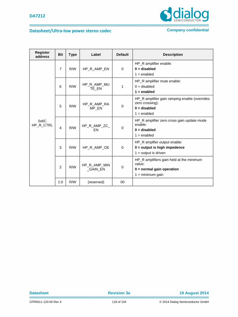
DA7212
Datasheet/Ultra-low power stereo codec Company confidential
Datasheet Revision 3a 19 August 2014
CFR0011-120-00 Rev 4 118 of 154 © 2014 Dialog Semiconductor GmbH
Register address
Bit Type Label Default Description
0x6C HP_R_CTRL
7 R/W HP_R_AMP_EN 0
HP_R amplifier enable:
0 = disabled
1 = enabled
6 R/W HP_R_AMP_MU
TE_EN 1
HP_R amplifier mute enable:
0 = disabled
1 = enabled
5 R/W HP_R_AMP_RA
MP_EN 0
HP_R amplifier gain ramping enable (overrides zero crossing):
0 = disabled
1 = enabled
4 R/W HP_R_AMP_ZC_
EN 0
HP_R amplifier zero cross gain update mode enable:
0 = disabled
1 = enabled
3 R/W HP_R_AMP_OE 0
HP_R amplfier output enable:
0 = output is high impedence
1 = output is driven
2 R/W HP_R_AMP_MIN
_GAIN_EN 0
HP_R amplifiers gain held at the minimum value:
0 = normal gain operation
1 = minimum gain
1:0 R/W (reserved) 00

DA7212
Datasheet/Ultra-low power stereo codec Company confidential
Datasheet Revision 3a 19 August 2014
CFR0011-120-00 Rev 4 119 of 154 © 2014 Dialog Semiconductor GmbH
Register address
Bit Type Label Default Description
0x6D LINE_CTRL
7 R/W LINE_AMP_EN 0
LINE amplifier enable:
0 = disabled
1 = enabled
6 R/W LINE_AMP_MUT
E_EN 1
LINE amplifier mute enable:
0 = disabled
1 = enabled
5 R/W LINE_AMP_RAM
P_EN 0
LINE amplifier gain ramping enable (overrides zero crossing):
0 = disabled
1 = enabled
4 R/W (reserved) 0
3 R/W LINE_AMP_OE 0
LINE amplfier output enable:
0 = output is high impedence
1 = output is driven
2 R/W LINE_AMP_MIN
_GAIN_EN 0
LINE amplifiers gain held at the minimum value:
0 = normal gain operation
1 = minimum gain
1:0 R/W (reserved) 00

DA7212
Datasheet/Ultra-low power stereo codec Company confidential
Datasheet Revision 3a 19 August 2014
CFR0011-120-00 Rev 4 120 of 154 © 2014 Dialog Semiconductor GmbH
Register address
Bit Type Label Default Description
0x6E MIXOUT_L_
CTRL
7 R/W MIXOUT_L_AMP
_EN 0
MIXOUT_L mixer amp enable:
0 = disabled
1 = enabled
6 R/W (reserved) 0
5 R/W (reserved) 0
4 R/W MIXOUT_L_SOF
TMIX_EN 1
MIXOUT L soft mix enable.
When enabled, the gain of any signal that is added to the mixer is ramped up or down at a rate determined by the GAIN_RAMP_RATE (0x92[1:0]) setting
0 = disabled
1 = enabled
3 R/W MIXOUT_L_MIX
_EN 0
MIXOUT L mixer enable:
0 = disabled
1 = enabled
2 R/W (reserved) 0
1:0 R/W (reserved) 00
Register address
Bit Type Label Default Description
0x6F MIXOUT_R_
CTRL
7 R/W MIXOUT_R_AM
P_EN 0
MIXOUT_R mixer amp enable:
0 = disabled
1 = enabled
6:5 R/W (reserved) 00
4 R/W MIXOUT_R_SOF
TMIX_EN 1
MIXOUT R soft mix enable.
When enabled, the gain of any signal that is added to the mixer is ramped up or down at a rate determined by the GAIN_RAMP_RATE (0x92[1:0]) setting
0 = disabled
1 = enabled
3 R/W MIXOUT_R_MIX
_EN 0
MIXOUT R mixer enable:
0 = disabled
1 = enabled
2:0 R/W (reserved) 000

DA7212
Datasheet/Ultra-low power stereo codec Company confidential
Datasheet Revision 3a 19 August 2014
CFR0011-120-00 Rev 4 121 of 154 © 2014 Dialog Semiconductor GmbH
Mixed Sample Mode Registers 15.4.4
Register Address
Bit Type Label Default Description
0x84 MIXED_SA
MPLE_MODE
7:1 R/W (reserved) 0000000
0 R/W 24_48_MODE 0
Enables the 24_48_MODE of operation. When this bit is asserted, 24_48_MODE is activated. The ADC path runs at 24kHz and the rest of the system, including the DAC path, at 48kHz.
Note: in 24_48_MODE, the system sample rate, which is controlled by bit SR at register address 0x22[3:0], must be set to 1010, or 48kHz. This will make the I2S also run at 48kHz and so the ADC output, running at 24 kHz, will be double sampled.
0 = Both ADC and DAC paths run at a speed determined by the setting of SR at 0x22[3:0]
1 = The ADC path runs at 24 kHz, and the DAC path at 48 kHz

DA7212
Datasheet/Ultra-low power stereo codec Company confidential
Datasheet Revision 3a 19 August 2014
CFR0011-120-00 Rev 4 122 of 154 © 2014 Dialog Semiconductor GmbH
Configuration Registers 15.4.5
Register address
Bit Type Label Defau
lt Description
0x90 LDO_CTRL
7 R/W LDO_EN 0
Audio sub-system digital LDO control. The master bias must be enabled for the LDO to operate. 0 = LDO bypassed
1 = LDO active
After powering up from Off or from Powerdown Mode, you must wait for a minimum of 40 ms after the first I2C access before enabling the LDO.
Failure to wait 40 ms can cause the chip to reset. All other I2C accesses are unaffected.
6 R/W (reserved) 0
5:4 R/W LDO_LEVEL_SELECT 00
Audio sub-system digital LDO level select: 0 = 1.05 V
1 = 1.10 V 2 = 1.20 V 3 = 1.40 V
3:0 R/W (reserved) 0

DA7212
Datasheet/Ultra-low power stereo codec Company confidential
Datasheet Revision 3a 19 August 2014
CFR0011-120-00 Rev 4 123 of 154 © 2014 Dialog Semiconductor GmbH
Register address
Bit Type Label Default Description
0x92 GAIN_RAMP_
CTRL
7:2 R/W (reserved) 000000
1:0 R/W GAIN_RAMP_RATE 00
Speed of the gain-ramping when activated.
00 = nominal rate / 8
(ramps from zero to maximum in about 1/128 second)
01 = nominal rate / 16
(fastest ramp rate. Ramps from zero to maximum in about 1/256 second)
10 = nominal rate * 16
(approximately 1 second fade-in from zero to maximum)
11 = nominal rate * 32
(slowest ramp rate, with approximately 2 second fade-in from zero to maximum)
The nominal rate is targeted to be approx 1.28ms per dB for the AUX, HP and LINE, and 0.64ms per 0.75 dB for the ADC, DAC and MIXOUT
Register address
Bit Type Label Default Description
0x93 MIC_CONFI
G
7 R/W (reserved) 0
6 R/W (reserved) 0
5:4 R/W (reserved) 00
3 R/W (reserved) 0
2 R/W DMIC_CLK_RAT
E 0
Clock rate for the digital microphone is:
0 = 3 MHz
1 = 1.5 MHz
1 R/W DMIC_SAMPLEP
HASE 0
Phase of the digital microphone:
0 = sample on DMICCLK edges
1 = sample between DMICCLK edges
0 R/W DMIC_DATA_SE
L 0
DMIC channel select
0 = rising L, falling R
1 = falling L, rising R

DA7212
Datasheet/Ultra-low power stereo codec Company confidential
Datasheet Revision 3a 19 August 2014
CFR0011-120-00 Rev 4 124 of 154 © 2014 Dialog Semiconductor GmbH
Register address
Bit Type Label Default Description
0x94 PC_COUNT
7:2 R/W (reserved) 000000
1 R/W PC_RESYNC_A
UTO 1
PC resync mode.
If the DAI clock drifts away from the system clock, this determines whether the system attempts to resynchronise the clocks (=1) or whether it skips a sample/samples twice (=0).
0 = freerun - double sample if the DAI clock is fast, or skip a sample if the DAI clock is slow
1 = autoresync upon detection of DAI drift with respect to the system clock
Note: Resynchronising (PC_RESYNC_AUTO = 1) can reduce the artifacts caused by jitter on either MCLK or BCLK
0 R/W PC_FREERUN 0
Enables the filter operation when DAI is not enabled or no DAI clocks are available (ADC to DAC processing path):
0 = ADC and DAC Filters synchronised to the DAI
1 = Filters free running
Note: This should be set to 1 if the ADC is feeding the DAC directly and no DAI clocks are present
Register address
Bit Type Label Default Description
0x95 CP_VOL_THRESHOLD1
7:6 R/W (reserved) 00
5:0 R/W CP_THRESH_V
DD2 100000
Threshold at and below which the charge pump can use the CPVDD/2 rail. Full details are given in section 14.15 on page 42
Note: This setting is only effective when CP_MCHANGE = 10 or CP_MCHANGE = 11. It is ignored for CP_MCHANGE settings of 00 and 01
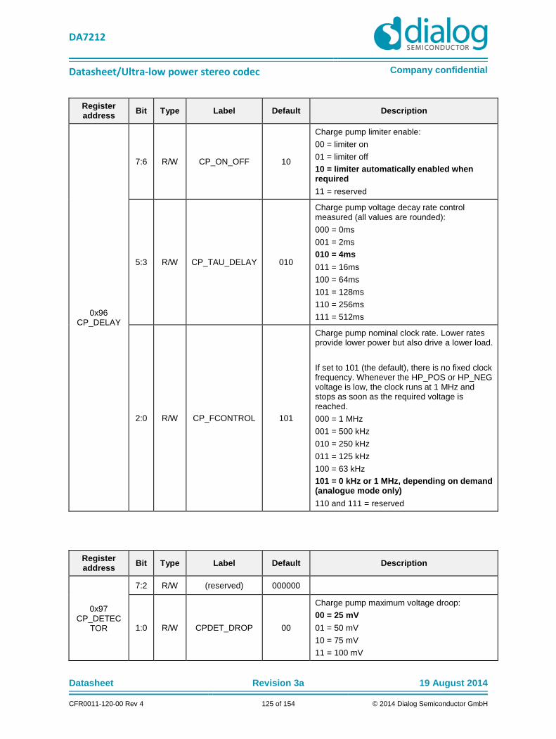
DA7212
Datasheet/Ultra-low power stereo codec Company confidential
Datasheet Revision 3a 19 August 2014
CFR0011-120-00 Rev 4 125 of 154 © 2014 Dialog Semiconductor GmbH
Register address
Bit Type Label Default Description
0x96 CP_DELAY
7:6 R/W CP_ON_OFF 10
Charge pump limiter enable:
00 = limiter on
01 = limiter off
10 = limiter automatically enabled when required
11 = reserved
5:3 R/W CP_TAU_DELAY 010
Charge pump voltage decay rate control measured (all values are rounded):
000 = 0ms
001 = 2ms
010 = 4ms
011 = 16ms
100 = 64ms
101 = 128ms
110 = 256ms
111 = 512ms
2:0 R/W CP_FCONTROL 101
Charge pump nominal clock rate. Lower rates provide lower power but also drive a lower load.
If set to 101 (the default), there is no fixed clock frequency. Whenever the HP_POS or HP_NEG voltage is low, the clock runs at 1 MHz and stops as soon as the required voltage is reached.
000 = 1 MHz
001 = 500 kHz
010 = 250 kHz
011 = 125 kHz
100 = 63 kHz
101 = 0 kHz or 1 MHz, depending on demand (analogue mode only)
110 and 111 = reserved
Register address
Bit Type Label Default Description
0x97 CP_DETEC
TOR
7:2 R/W (reserved) 000000
1:0 R/W CPDET_DROP 00
Charge pump maximum voltage droop:
00 = 25 mV
01 = 50 mV
10 = 75 mV
11 = 100 mV

DA7212
Datasheet/Ultra-low power stereo codec Company confidential
Datasheet Revision 3a 19 August 2014
CFR0011-120-00 Rev 4 126 of 154 © 2014 Dialog Semiconductor GmbH
Register address
Bit Type Label Default Description
0x98 DAI_OFFSE
T 7:0 R/W DAI_OFFSET
00000000
DAI data offset with respect to WCLK. If set to 0, no offset will be inserted relative to the normal formatting.
The DAI data offset is measured in BCLK cycles.
Register address
Bit Type Label Default Description
0x99 DIG_CTRL
7 R/W DAC_R_INV 0 0 = DAI right input stream is not inverted
1 = DAI right input stream is inverted
6:4 R/W (reserved) 000
3 R/W DAC_L_INV 0 0 = DAI left input stream is not inverted
1 = DAI left input stream is inverted
2:0 R/W (reserved) 000

DA7212
Datasheet/Ultra-low power stereo codec Company confidential
Datasheet Revision 3a 19 August 2014
CFR0011-120-00 Rev 4 127 of 154 © 2014 Dialog Semiconductor GmbH
Register address
Bit Type Label Default Description
0x9A ALC_CTRL2
7:4 R/W ALC_RELEASE 0000
Sets the ALC release rate. This is the speed at which the ALC can increase the gain by 1 dB.
0000 = 29/fs (0.6ms/dB @48 kHz)
0001 = 57/fs (1.2ms/dB @48 kHz)
0010 = 115/fs (2.4ms/dB @48 kHz)
0011 = 229/fs (4.8ms/dB @48 kHz)
0100 = 459/fs (9.6ms/dB @48 kHz)
0101 = 917/fs (19.1ms/dB @48 kHz)
0110 = 1834/fs (38.2ms/dB @48 kHz)
0111 = 3669/fs (76.4ms/dB @48 kHz)
1000 = 7338/fs (153ms/dB @48 kHz)
1001 = 14676/fs (306ms/dB @48 kHz)
1010 to 11111 = 29347/fs (611ms/dB @48 kHz)
3:0 R/W ALC_ATTACK 0000
Sets the ALC attack rate, which is the speed at which the ALC can decrease the gain by 1 dB.
0000 = 7.3/fs (0.15ms/dB @48 kHz)
0011 = 15/fs (0.31ms/dB @48 kHz)
0010 = 29/fs (0.61ms/dB @48 kHz)
0011 = 59/fs (1.2ms/dB @48 kHz)
0100 = 117/fs (2.4ms/dB @48 kHz)
0101 = 235/fs (4.9ms/dB @48 kHz)
0110 = 469/fs (9.8ms/dB @48 kHz)
0111 = 938/fs (20ms/dB @48 kHz)
1000 = 1876/fs (39ms/dB @48 kHz)
1001 = 3753/fs (78ms/dB @48 kHz)
1010 = 7506/fs (156ms/dB @48 kHz)
1011 = 15012/fs (312ms/dB @48 kHz)
1100 to 1111 = 30024/fs (625ms/dB @48 kHz)

DA7212
Datasheet/Ultra-low power stereo codec Company confidential
Datasheet Revision 3a 19 August 2014
CFR0011-120-00 Rev 4 128 of 154 © 2014 Dialog Semiconductor GmbH
Register address
Bit Type Label Default Description
0x9B ALC_CTRL3
7:6 R/W ALC_INTEG_RE
LEASE 00
Sets the rate at which the input signal envelope is tracked as the signal gets smaller
00 = 1/4
01 = 1/16
10 = 1/256
11 = Reserved (Do not use)
5:4 R/W ALC_INTEG_AT
TACK 00
Sets the rate at which the input signal envelope is tracked as the signal gets larger:
00 = 1/4
01 = 1/16
10 = 1/256
11 = Reserved (Do not use)
3:0 R/W ALC_HOLD 0000
Sets the ALC hold time, which is the the length of time that the ALC waits before releasing
0000 = 62/fs (1.3ms @48 kHz)
0001 = 124/fs (2.6ms @48 kHz)
0010 = 248/fs (5.2ms @48 kHz)
0011 = 496/fs (10.3ms @48 kHz)
0100 = 992/fs (20.7ms @48 kHz)
0101 = 1984/fs (41.3ms @48 kHz)
0110 = 3968/fs (82.7ms @48 kHz)
0111 = 7936/fs (165ms @48 kHz)
1000 = 15872/fs (331ms @48 kHz)
1001 = 31744/fs (661ms @48 kHz)
1010 = 63488/fs (1.3s @48 kHz)
1011 = 126976/fs (2.6s @48 kHz)
1100 = 253952/fs (5.3s @48 kHz)
1101 = 507904/fs (10.6s @48 kHz)
1110 = 1015808/fs (21s @48 kHz)
1111 = 2031616/fs (42s @48 kHz)

DA7212
Datasheet/Ultra-low power stereo codec Company confidential
Datasheet Revision 3a 19 August 2014
CFR0011-120-00 Rev 4 129 of 154 © 2014 Dialog Semiconductor GmbH
Register address
Bit Type Label Default Description
0x9C ALC_NOISE
7:6 R/W (reserved) 00
5:0 R/W ALC_NOISE 111111
Sets the threshold below which input signals will not cause the ALC to change gain:
000000 = 0 dBFS
000001 = -1.5 dBFS
continuing in -1.5 dBFS steps to
111111 = -94.5 dBFS
Register address
Bit Type Label Default Description
0x9D ALC_TARG
ET_MIN
7:6 R/W (reserved) 00
5:0 R/W ALC_THRESHO
LD_MIN 111111
Sets the minimum amplitude of the ALC output signal before the ALC increases the gain. If the maximum allowable gain level is reached then the ALC will not increase the gain even if this threshold is breached:
000000 = 0 dBFS
000001 = -1.5 dBFS
continuing in -1.5 dBFS steps to
111111 = -94.5 dBFS

DA7212
Datasheet/Ultra-low power stereo codec Company confidential
Datasheet Revision 3a 19 August 2014
CFR0011-120-00 Rev 4 130 of 154 © 2014 Dialog Semiconductor GmbH
Register address
Bit Type Label Default Description
0x9E ALC_TARG
ET_MAX
7:6 R/W (reserved) 00
5:0 R/W ALC_THRESHO
LD_MAX 000000
Sets the maximum amplitude of the ALC output signal before the ALC decreases the gain. If the maximum attenution level allowed is reached then the ALC will not reduce the gain even if this threshold is exceeded:
000000 = 0 dBFS
000001 = -1.5 dBFS
continuing in -1.5 dB steps to
111111 = -94.5 dBFS
Register address
Bit Type Label Default Description
0x9F ALC_GAIN_
LIMITS
7:4 R/W ALC_GAIN_MAX 1111
Sets the maximum amount of gain that can be applied to the input signal by the ALC when the input signal amplitude is smaller than ALC_THRESHOLD_MIN:
0000 = 0 dB
0001 = 6 dB
continuing in +6 dB steps to
1111 = 90 dB
3:0 R/W ALC_ATTEN_MA
X 1111
Sets the maximum amount of attenuation that can be applied to the input signal by the ALC when the input signal amplitude is larger than ALC_THRESHOLD_MAX:
0000 = 0 dB
0001 = 6 dB
continuing in +6 dB steps to
1111 = 90 dB

DA7212
Datasheet/Ultra-low power stereo codec Company confidential
Datasheet Revision 3a 19 August 2014
CFR0011-120-00 Rev 4 131 of 154 © 2014 Dialog Semiconductor GmbH
Register address
Bit Type Label Default Description
7 R/W (reserved) 0
0XA0 ALC_ANA_GAIN_LIMITS
6:4 R/W ALC_ANA_GAIN
_MAX 111
Sets the maximum amount of analogue gain that can be applied to the input signal by the ALC when the input signal amplitude is smaller than ALC_THRESHOLD_MIN:
000 = reserved
001 = 0 dB
010 = 6 dB
continuing in +6 dB steps to
111 = 36 dB
3 R/W (reserved) 0
2:0 R/W ALC_ANA_GAIN
_MIN 001
Sets the minimum amount of analogue gain that can be applied to the input signal by the ALC when the input signal amplitude is larger than ALC_THRESHOLD_MAX:
000 = reserved
001 = 0 dB
010 = 6 dB
continuing in +6 dB steps to
111 = 36 dB
Register address
Bit Type Label Default Description
0xA1 ALC_ANTICLIP_CTRL
7 R/W ALC_ANTICLIP_
EN 0
Enables the ALC signal clip prevention mechanism:
0 = Disabled
1 = Enabled
6:2 R/W (reserved) 00000
1:0 R/W (reserved) 00

DA7212
Datasheet/Ultra-low power stereo codec Company confidential
Datasheet Revision 3a 19 August 2014
CFR0011-120-00 Rev 4 132 of 154 © 2014 Dialog Semiconductor GmbH
Register address
Bit Type Label Default Description
0xA2 ALC_ANTICLIP_LEVEL
7 R/W (reserved) 0
6:0 R/W ALC_ANTICLIP_
LEVEL 0000000
Sets the threshold above which the ALC enters anti-clip operation. The formula for determining the anti-clip level is:
(ALC_ANTICLIP_LEVEL+1)*Full Scale/128
0000000 = 0.0078*Full Scale
0000001 = 0.015*Full Scale
continuing in 0.0078 steps to
1111111 = 1.0000*Full Scale
Register address
Bit Type Label Default Description
0xAF DAC_NG_SETUP_TIME
7:4 R/W (reserved) 0000
3 R/W DAC_NG_RAMP
DN_RATE 0
Attack rate at which the gain of the output amplifier (HP or LINE) is reduced:
0 = 0.64 ms/dB
1 = 20.48 ms/dB
2 R/W DAC_NG_RAMP
UP_RATE 0
Release rate at which the gain of the ouput amplifier (HP or LINE) is increased:
0 = 0.02 ms/dB
1 = 0.16 ms/dB
1:0 R/W DAC_NG_SETU
P_TIME 00
Time for which the largest signal through the DACs must be below DAC_NG_ON_THRESHOLD for the noise-gate to mute the data:
00 = 256 samples
01 = 512 samples
10 = 1024 samples
11 = 2048 samples

DA7212
Datasheet/Ultra-low power stereo codec Company confidential
Datasheet Revision 3a 19 August 2014
CFR0011-120-00 Rev 4 133 of 154 © 2014 Dialog Semiconductor GmbH
Register address
Bit Type Label Default Description
0xB0 DAC_NG_OFF_THRESH
OLD
7:3 R/W (reserved) 00000
2:0 R/W DAC_NG_OFF_
THRESHOLD 000
Threshold above which the noise-gate will be deactivated:
000 = -90 dB
001 = -84 dB
…
111 = -48 dB
Register address
Bit Type Label Default Description
0xB1 DAC_NG_ON_THRESH
OLD
7:3 R/W (reserved) 00000
2:0 R/W DAC_NG_ON_T
HRESHOLD 000
Threshold below which the noise-gate starts to activate:
000 = -90 dB
001 = -84 dB
…
111 = -48 dB
Register address
Bit Type Label Default Description
0xB2 DAC_NG_C
TRL
7 R/W DAC_NG_EN 0
DAC noise-gate enable:
0 = disabled
1 = enabled
6:0 R/W (reserved) 0000000

DA7212
Datasheet/Ultra-low power stereo codec Company confidential
Datasheet Revision 3a 19 August 2014
CFR0011-120-00 Rev 4 134 of 154 © 2014 Dialog Semiconductor GmbH
Register address
Bit Type Label Default Description
0xB4 TONE_GEN
_CFG1
7 R/W START_STOPN 0
Tone generator stop and start control.
Setting this to high will start the tone-generator. After the tone-generator has finished it will reset the register to 0. In Continuous mode, setting it to 0 will stop the tone generation.
6:5 R/W (reserved) 00
4 R/W DMTF_EN 0
DTMF enable 0 = Use values in the FREQ1 and FREQ2 registers to generate sine wave(s)
1 = Use values from the DMTF_REG to generate sine-waves
3:0 R/W DMTF_REG 0000 The DTMF key pad values 0 to 15.
Register address
Bit Type Label Default Description
0xB5 TONE_GEN
_CFG2
7:4 R/W GAIN 0000
0000 = 0 dB
0001 = -3 dB 0010 = -6 dB 0011 = -9 dB
continuing in -3 dB steps to
1111 = -45 dB
3:2 R/W (reserved) 00
1:0 R/W SWG_SEL 00
Sine wave select: 00 = Sum of both SWG values is mixed into the audio
01 = Only SWG1 value is output 10 = Only SWG2 value is output 11 = Sum of both SWG values is mixed into the audio.

DA7212
Datasheet/Ultra-low power stereo codec Company confidential
Datasheet Revision 3a 19 August 2014
CFR0011-120-00 Rev 4 135 of 154 © 2014 Dialog Semiconductor GmbH
Register address
Bit Type Label Default Description
0xB6 TONE_GEN_CYCLES
7:3 R/W (reserved) 00000
2:0 R/W BEEP_CYCLES 000
Number of beep cycles required.
000 = 1 cycle
001 = 2 cycles
010 = 4 cycles
011 = 8 cycles
100 = 16 cycles
101 = 32 cycles
110 and 111 = infinite (until START_STOPN is set to 0)
Register address
Bit Type Label Default Description
0xB7 TONE_GEN_FREQ1_L
7:0 R/W FREQ1_L 0x55
Lower two bytes of the four-byte number used to calculate the output frequency for the first Sine Wave Generator (SWG1). The output frequency is dependent on the sample rate
For sample rates (SR) = 8/12/16/24/32/48/96 kHz:
FREQ1_U & FREQ1_L = (2^16 * (fHZ/12000)) -1
For sample rates (SR) = 11.025/22.05/44.4/88.2 kHz:
FREQ1_U & FREQ1_L =(2^16 * (fHZ/11025)) -1

DA7212
Datasheet/Ultra-low power stereo codec Company confidential
Datasheet Revision 3a 19 August 2014
CFR0011-120-00 Rev 4 136 of 154 © 2014 Dialog Semiconductor GmbH
Register address
Bit Type Label Default Description
0xB8 TONE_GEN_FREQ1_U
7:0 R/W FREQ1_U 0x15
Upper two bytes of the four-byte number used to calculate the output frequency for the first Sine Wave Generator (SWG1). The output frequency is dependent on the sample rate
For sample rates (SR) = 8/12/16/24/32/48/96 kHz:
FREQ1_U & FREQ1_L = (2^16 * (fHZ/12000)) -1
For sample rates (SR) = 11.025/22.05/44.4/88.2 kHz:
FREQ1_U & FREQ1_L =(2^16 * (fHZ/11025)) -1
Register address
Bit Type Label Default Description
0xB9 TONE_GEN_FREQ2_L
7:0 R/W FREQ2_L 0x00
Lower two bytes of the four-byte number used to calculate the output frequency for the second Sine Wave Generator (SWG2). The output frequency is dependent on the sample rate
For sample rates (SR) = 8/12/16/24/32/48/96 kHz:
FREQ2_U & FREQ2_L = (2^16 * (fHZ/12000)) -1
For sample rates (SR) = 11.025/22.05/44.4/88.2 kHz
FREQ2_U & FREQ2_L =(2^16 * (fHZ/11025)) -1

DA7212
Datasheet/Ultra-low power stereo codec Company confidential
Datasheet Revision 3a 19 August 2014
CFR0011-120-00 Rev 4 137 of 154 © 2014 Dialog Semiconductor GmbH
Register address
Bit Type Label Default Description
0xBA TONE_GEN_FREQ2_U
7:0 R/W FREQ2_U 0x40
Upper two bytes of the four-byte number used to calculate the output frequency for the second Sine Wave Generator (SWG2). The output frequency is dependent on the sample rate
For sample rates (SR) = 8/12/16/24/32/48/96 kHz:
FREQ2_U & FREQ2_L = (2^16 * (fHZ/12000)) -1
For sample rates (SR) = 11.025/22.05/44.4/88.2 kHz
FREQ2_U & FREQ2_L =(2^16 * (fHZ/11025)) -1
Register address
Bit Type Label Default Description
0xBB TONE_GEN_ON_PER
7:6 R/W (reserved) 00
5:0 R/W BEEP_ON_PER 02
Beep ‘On’ period
0x00 = Reserved
0x01 = 10ms 0x02 = 20ms
0x03 = 30ms
Continuing in 10ms steps to
0x20 = 200ms
0x21 = Reserved
0x22 = Reserved
0x23 = Reserved
0x24 = Reserved
Then in 50ms steps from
0x25 = 250ms
to 0x60 = 2000msec
0x61 = Reserved
0x62 = Reserved
0x63 = continuous
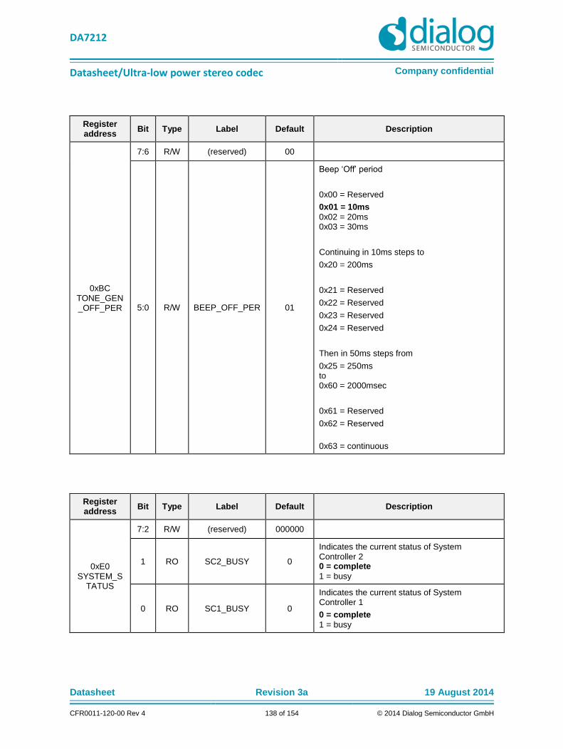
DA7212
Datasheet/Ultra-low power stereo codec Company confidential
Datasheet Revision 3a 19 August 2014
CFR0011-120-00 Rev 4 138 of 154 © 2014 Dialog Semiconductor GmbH
Register address
Bit Type Label Default Description
0xBC TONE_GEN_OFF_PER
7:6 R/W (reserved) 00
5:0 R/W BEEP_OFF_PER 01
Beep ‘Off’ period
0x00 = Reserved
0x01 = 10ms
0x02 = 20ms 0x03 = 30ms
Continuing in 10ms steps to
0x20 = 200ms
0x21 = Reserved
0x22 = Reserved
0x23 = Reserved
0x24 = Reserved
Then in 50ms steps from
0x25 = 250ms to 0x60 = 2000msec
0x61 = Reserved
0x62 = Reserved
0x63 = continuous
Register address
Bit Type Label Default Description
0xE0 SYSTEM_S
TATUS
7:2 R/W (reserved) 000000
1 RO SC2_BUSY 0
Indicates the current status of System Controller 2 0 = complete
1 = busy
0 RO SC1_BUSY 0
Indicates the current status of System Controller 1
0 = complete
1 = busy

DA7212
Datasheet/Ultra-low power stereo codec Company confidential
Datasheet Revision 3a 19 August 2014
CFR0011-120-00 Rev 4 139 of 154 © 2014 Dialog Semiconductor GmbH
Register address
Bit Type Label Default Description
0xFD SYSTEM_A
CTIVE
7:1 R/W (reserved) 0000000
0 R/W SYSTEM_ACTIV
E 0
Switch off the oscillator 0 = oscillator off
1 = oscillator on

DA7212
Datasheet/Ultra-low power stereo codec Company confidential
Datasheet Revision 3a 19 August 2014
CFR0011-120-00 Rev 4 140 of 154 © 2014 Dialog Semiconductor GmbH
16 Package information
Figure 35: DA7212 package outline drawing

DA7212
Datasheet/Ultra-low power stereo codec Company confidential
Datasheet Revision 3a 19 August 2014
CFR0011-120-00 Rev 4 141 of 154 © 2014 Dialog Semiconductor GmbH
17 Ordering information
The ordering number consists of the part number followed by a suffix indicating the packing method. For details and availability, please consult your local sales representative.
Table 36: Ordering information
Part Number Package Shipment Form Pack quantity
DA7212-01UM2 34-bump CSP Pb-free/green
T & R 4500

DA7212
Datasheet/Ultra-low power stereo codec Company confidential
Datasheet Revision 3a 19 August 2014
CFR0011-120-00 Rev 4 142 of 154 © 2014 Dialog Semiconductor GmbH
Appendix A Applications information
A.1 Codec initialisation
Depending on the specific application, some general settings need to be set. Examples of these settings include the sample rate, the PLL, and the Digital Audio Interface. Then the amplifiers, the mixers and channels of the ADC/DAC have to be configured and enabled via their respective control registers.
An example sequence is shown below:
1. Configure clock mode as required for operation, (e.g. PLL bypass / PLL etc…)
2. Configure the digital audio interface
3. Configure the charge pump if the headphone path is in use.
4. Set input and output mixer paths and gains
5. Enable Input and Output paths using the Level 2 System Controller (SLC2)
A.2 Automatic ALC calibration
When using the automatic level control (ALC) in sync-mode the DC offset between the digital and analogue PGAs must be cancelled. This is performed automatically if the following procedure is performed:
1. Enable Microphone amplifiers unmuted
2. Mute microphones
3. Enable Input mixer and ADC unmuted
4. Enable AIF interface
5. Set ALC_AUTO_CALIB_EN in ALC_CTRL1 to ‘1’ (ALC_CTRL1 = 0x10). This bit will auto-clear when calibration is complete.
6. When calibration is complete, enable the ALC with ALC_SYNC_MODE and ALC_OFFSET_EN enabled (ALC_CTRL1 = 0x8b).
7. Unmute microphones

DA7212
Datasheet/Ultra-low power stereo codec Company confidential
Datasheet Revision 3a 19 August 2014
CFR0011-120-00 Rev 4 143 of 154 © 2014 Dialog Semiconductor GmbH
Appendix B Components
The following recommended components are examples selected from requirements of a typical application. The electrical characteristics (that is, the supported voltage/current ranges) have to be cross-checked and component types may need to be adapted from the individual needs of the target circuitry.
B.1 Audio inputs
Table 37: Audio inputs
Pin Name Bump/Pin Power Domain Description Type
MIC1_P
C17 VDD_A Differential mic. input 1 (positive) / Single-ended mic. Input 1 (left)
Analogue Input
MIC1_N
B16 VDD_A Differential mic. input 1 (negative) / Single-ended mic. Input 2 (left)
Analogue Input
MIC2_P D16 VDD_A Differential mic. input 2 (positive) / Single-ended mic. Input 1 (right)
Analogue Input
MIC2_N C15 VDD_A Differential mic. input 2 (negative) / Single-ended mic. Input 2 (right)
Analogue Input
AUX_L C13 VDD_A Single-ended auxiliary input (left) Analogue Input
AUX_R D14 VDD_A Single-ended auxiliary input (right)
Analogue Input
The DA7212 microphone inputs can be configured to accommodate single-ended or differential microphones and line inputs. These are accompanied by two dedicated single ended auxiliary input pins.
The internal input mixer allows all inputs to be mixed prior to the ADC. Analogue bypass paths exist directly from the AUX inputs to the output mixers and from the input mixer to the output mixer should the ADC not be required.
A DC blocking capacitor is required for each used analogue input bump used in the target application. The choice of capacitor is determined by the filter that is formed between that capacitor and the input impedance of the input pin which can be found in the ‘Input Mixing Units’ section of the datasheet.
Where Fc is the 3 dB cut off frequency of the low pass filter (typically 20Hz for audio applications). A 1µF capacitor is suitable for most applications.
Due to their high stability tantalum capacitors are particularly suitable for this application. Ceramic equivalents with an X5R dielectric are recommended as a cost effective alternative. Care should be taken to ensure that the desired capacitance is maintained over operating temperature and voltage.

DA7212
Datasheet/Ultra-low power stereo codec Company confidential
Datasheet Revision 3a 19 August 2014
CFR0011-120-00 Rev 4 144 of 154 © 2014 Dialog Semiconductor GmbH
Z5U dielectric ceramics should be avoided due to their susceptibility to microphonic effects.
Unused input bumps can be left floating or connected via a capacitor to ground.
B.2 Microphone Bias
Table 38: Microphone bias
Pin Name Bump/Pin Power Domain Description Type
MICBIAS1
A15 VDD_MIC Microphone bias output 1 Analogue Output
MICBIAS2 A17 VDD_MIC Microphone bias output 2 Analogue Output
A 1µF capacitor to GND_A should be used to decouple the MICBIAS output.
MICBIAS1M11MICBIAS1µF
MICBIAS2A17MICBIAS 21µF
A15MICBIAS 1
Figure 36 Micbias decoupling
B.3 Digital Microphone
Table 39: Digital microphones
Pin Name Bump/Pin Power Domain Description Type
DMICCLK
C17 VDD_MIC Digital Microphone Clock Digital Output
DMICIN
B16 VDD_MIC Digital Microphone Data Digital Input
These pins can be routed directly to a digital microphone. In stereo mode they can be connected to two digital microphones with one configured to send data on the rising clock edge and the other on the falling edge. The clock output operates at 1.5 MHz or 3 MHz. The appropriate layout considerations for clock signals should be followed.

DA7212
Datasheet/Ultra-low power stereo codec Company confidential
Datasheet Revision 3a 19 August 2014
CFR0011-120-00 Rev 4 145 of 154 © 2014 Dialog Semiconductor GmbH
B.4 Audio Outputs
Table 40: Headphone outputs
Pin Name Bump/Pin Power Domain Description Type
HP_L A3 VDD_A True-ground headphone output (left)
Analogue Output
HP_R A5 VDD_A True-ground headphone output (right)
Analogue Output
GND_SENSE B4 VDD_A Ground reference for headphone output
Analogue Input
DA7212 contains a capless true-ground Class-G headphone amplifier with a ground sense connection. For optimum noise immunity the headphone ground sense should be tracked between the HP_L and HP_R signals before being grounded at the headphone connector. In this configuration the ground sense connector cancels common mode noise on the headphone from the PCB.
M11MICBIAS
A5HP_R
A3HP_LGND_SENSE B4
Figure 37 Recommended Headphone layout
Table 41: Speaker outputs
Pin Name Bump/Pin Power Domain Description Type
SP_P
B12 VDD_SP Differential speaker output (pos) Analogue Output
SP_N
A13 VDD_SP Differential speaker output (neg) Analogue Output
The DA7212 has a differential Class-AB speaker driver that can output 1.2W into an 8ohm speaker.
These pins can be connected directly to an external speaker or receiver or as a differential line
output. For common mode noise immunity SP_P and SP_N should be treated as a differential pair
where possible.
A DC blocking capacitor is required when the speaker is being used to drive a line level output. The
choice of capacitor is determined by the filter that is formed between that capacitor and the
impedance of the load.

DA7212
Datasheet/Ultra-low power stereo codec Company confidential
Datasheet Revision 3a 19 August 2014
CFR0011-120-00 Rev 4 146 of 154 © 2014 Dialog Semiconductor GmbH
Where Fc is the 3 dB cut off frequency of the low pass filter (typically 20Hz for audio applications). A
1µF capacitor is suitable for most applications.
Due to their high stability tantalum capacitors are particularly suitable for this application. Ceramic
equivalents with an X5R dielectric are recommended as a cost effective alternative. Care should be
taken to ensure that the desired capacitance is maintained over operating temperature and voltage.
If the speaker/line output is unused the output pins can be left floating or connected via a capacitor
to ground.
B.5 Headphone Charge pump
Table 42: Headphone charge pump
Pin Name Bump/Pin Power Domain Description Type
HPCSP A1 VDD_A Chargepump reservoir capacitor (pos) Charge Pump
HPCSN C1 VDD_A Chargepump reservoir capacitor (neg) Charge Pump
HPCFP D2 VDD_A Chargepump flying capacitor (pos) Charge Pump
HPCFN C3 VDD_A Chargepump flying capacitor (neg) Charge Pump
A 1µF reservoir capacitor is required between the HPCSP and GND_CP and between HPCSN and GND_CP. For best performance the capacitors should be fitted as near to the device as possible.
M11MICBIAS1µF
C1HPCSN1µF
A1HPCSP
Figure 38 Charge Pump Decoupling
A 1µF flying capacitor is required between HPCFP and HPCFN. For best performance the capacitor should be fitted as near to the device as possible.
M11MICBIAS1µF
C3HPCFN
D2HPCFP
Figure 39 Charge Pump Flying Capacitor

DA7212
Datasheet/Ultra-low power stereo codec Company confidential
Datasheet Revision 3a 19 August 2014
CFR0011-120-00 Rev 4 147 of 154 © 2014 Dialog Semiconductor GmbH
To ensure stable charge pump operation the effective series resistance of the flying capacitor should be kept to a minimum. This can be achieved by selecting an appropriate capacitor dielectric (X5R, X7R) and ensuring that the capacitor is placed as near to the device as possible. Ideally the connection between the pins and the capacitor should not run through Vias (connected on top layer of PCB only).
B.6 Digital Interfaces
Table 43: Digital interfaces – I2C
Pin Name Bump/Pin Power Domain Description Type
SDA C9 VDD_IO I2C bidirectional data Digital Input / Output
SCL D8 VDD_IO I2C clock input Digital Input
The I2C data and clock lines are powered from VDD_IO. Both I2C line require a pull up to VDD_IO. The value of this pull up is dependent on I2C bus speed, bus length and supply voltage. A 2.2 kΩ resistor is satisfactory in most applications.
SCLSDA C9
D8
VDD_IO
2k2Ω 2k2Ω
Figure 40 I2C pull ups
B.7 Capacitor Selection
Ceramic capacitors are manufactured with a variety of dielectrics, each with a different behaviour over temperature and applied voltage. Capacitors must have a dielectric adequate to ensure the minimum capacitance over the necessary temperature range, dc bias conditions and low Equivalent Series Resistance (ESR). X5R or X7R dielectrics with a voltage rating of 6.3 V or 10 V are recommended for best performance. Y5V and Z5U dielectrics are not recommended for use because of their poor temperature and dc bias characteristics.
The worst-case capacitance accounting for capacitor variation over temperature, component tolerance, and voltage is calculated using the following equation:
( ) ( )
where: CEFF is the effective capacitance at the operating voltage. TEMPCO is the worst-case capacitor temperature coefficient. TOL is the worst-case component tolerance. These figures can be found in the manufacturer’s datasheet.
In the example below, the worst-case temperature coefficient (TEMPCO) over −55°C to +85°C is assumed to be 15 %. The tolerance of the capacitor (TOL) is assumed to be 10 %, and COUT is 0.65 μF at 1.8 V.
Substituting these values in the equation yields

DA7212
Datasheet/Ultra-low power stereo codec Company confidential
Datasheet Revision 3a 19 August 2014
CFR0011-120-00 Rev 4 148 of 154 © 2014 Dialog Semiconductor GmbH
( ) ( )
Below is a table with recommended capacitor types:
Application Value Size Temp.
Char. Tolerance
Rated
Voltage Type
VDD_IO, VREF, VDD_MIC, VDD_SP,
VDD_A, VDIG, DACREF, VMID, HPCFP/HPCFN,
HPCSP, HPCSN,
MICBIAS1, MICBIAS2,
AUX_L, AUX_R
14x 1µF 0201 X5R +/-
15 % +/-10 % 6.3V Murata GRM033R60J105M

DA7212
Datasheet/Ultra-low power stereo codec Company confidential
Datasheet Revision 3a 19 August 2014
CFR0011-120-00 Rev 4 149 of 154 © 2014 Dialog Semiconductor GmbH
Appendix C Calibration Routine
The calibration routine requires the full signal path from microphone to ADC to be enabled and a clock to be present. The calibration routine using MIC1_P and MIC2_P and with the device in slave mode is outlined in Table 44.
Table 44: Offset calibration, MIC1_P and MIC2_P single ended, slave mode
Instruction Registers
affected Value
1. Enable Master Bias 0x23 0x80
2. Enable AIF and setup clocks (for 44.1 kHz, I2S, slave mode) 0x29 0xC8
3. Enable the Microphones unmuted 0x63
0x64
0x84
0x84
4. Mute the microphones 0x63
0x64
0xC4
0xC4
5. Enable the Input mixers unmuted 0x65
0x66
0xA8
0xA8
6. Route the microphone to the mixers 0x32
0x33
0x04
0x04
7. Enable the ADC unmuted 0x67
0x68
0xA0
0xA0
8. Calibrate Offset 0x2B 0x10
9. Wait until offset bit has been cleared Wait until 0x2B = 0x00
10. Enable ALC 0x2B 0x8B
11. Unmute Microphones 0x63
0x64
0xA8
0xA8
Other clocking and microphone setups are also possible by changing their respective registers. Once this calibration is complete the record path with Automatic Level Control is active.
C.1 Troubleshooting
0x2B should automatically clear after 256 samples (5.33ms at 48 kHz). If 0x2B does not return 0x00 after 256 samples this indicates a setup error. If this occurs check that the microphone is enabled and muted, the mixer is enabled with the microphone input selected and unmuted and that the ADC is enabled and unmuted. It is also critical that an MCLK and BCLK are present on the device. BCLK can be provided either from the AIF interface in slave mode or generated internally by having the device in master mode.
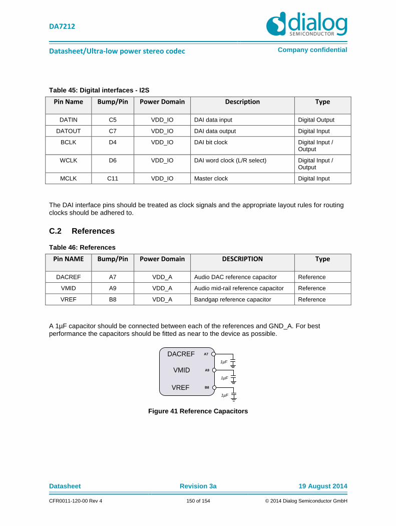
DA7212
Datasheet/Ultra-low power stereo codec Company confidential
Datasheet Revision 3a 19 August 2014
CFR0011-120-00 Rev 4 150 of 154 © 2014 Dialog Semiconductor GmbH
Table 45: Digital interfaces - I2S
Pin Name Bump/Pin Power Domain Description Type
DATIN C5 VDD_IO DAI data input Digital Output
DATOUT C7 VDD_IO DAI data output Digital Input
BCLK D4 VDD_IO DAI bit clock Digital Input / Output
WCLK D6 VDD_IO DAI word clock (L/R select) Digital Input / Output
MCLK C11 VDD_IO Master clock Digital Input
The DAI interface pins should be treated as clock signals and the appropriate layout rules for routing clocks should be adhered to.
C.2 References
Table 46: References
Pin NAME Bump/Pin Power Domain DESCRIPTION Type
DACREF A7 VDD_A Audio DAC reference capacitor Reference
VMID A9 VDD_A Audio mid-rail reference capacitor Reference
VREF B8 VDD_A Bandgap reference capacitor Reference
A 1µF capacitor should be connected between each of the references and GND_A. For best performance the capacitors should be fitted as near to the device as possible.
M11MICBIAS1µF
B8VREF1µF
A9VMID
A7
1µF
DACREF
Figure 41 Reference Capacitors

DA7212
Datasheet/Ultra-low power stereo codec Company confidential
Datasheet Revision 3a 19 August 2014
CFR0011-120-00 Rev 4 151 of 154 © 2014 Dialog Semiconductor GmbH
C.3 Supplies
Table 47: Power supplies
Pin NAME Bump/Pi
n
Power Domain DESCRIPTION Type
VDD_A B6 Min: 1.7 V
Max: 2.5 V
Supply for analogue circuits / Supply for headphone chargepump
Power Supply
VDD_IO D10 Min: 1.6 V
Max: 3.6 V Supply for digital interfaces Power Supply
VDD_SP A11 Min: 0.95 V
Max: 5.25 V Supply for speaker driver Power Supply
VDD_MIC B14 Min: 1.8 V
Max: 3.6 V Supply for microphone bias circuits Power Supply
VDIG D12 Output of internal regulator. Power Supply
Decoupling capacitors are recommended between all supplies and GND_A. These capacitors should be located as near to the device as possible.
M11MICBIAS
1µF
D12VDIG1µF
B14VDD_MIC
A11
1µF
VDD_SP
D10
1µF
VDD_IO
B6
1µF
VDD_A 1.7 V - 2.5 V
0.95 V - 5.25 V
1.8 V - 3.6 V
1.6 V - 3.6 V
Figure 42 Power Supply Decoupling
C.4 Ground
Table 48: Ground
Pin NAME Bump/Pin Power Domain DESCRIPTION Type
GND_A B10 Analogue ground Power Ground
GND_CP B2 Chargepump/digital ground Power Ground
GND_A and GND_CP should be connected directly to the system ground.

DA7212
Datasheet/Ultra-low power stereo codec Company confidential
Datasheet Revision 3a 19 August 2014
CFR0011-120-00 Rev 4 152 of 154 © 2014 Dialog Semiconductor GmbH
Appendix D PCB Layout Guidelines
DA7212 uses Dialog Semiconductor’s ‘Route Easy™’ technology allowing the device to be routed using conventional, low cost, PCB technology. All device balls are routable on the top level and conventional plated through hole vias can be used throughout.
This design is fully realisable using a 2-layer PCB however for optimum performance it is recommended that a 4-layer PCB is used with layers 2 and 3 as solid ground planes.
Decoupling and reference capacitors should be located as close to the device as possible and appropriately sized tracks should be used for all power connections.
Figure 43 DA7212 Example Layout
D.1 Layout and Schematic support
Copies of the evaluation board schematics and layout are available on request to aid in PCB development. Dialog Semiconductor also offer a schematic and layout review service for all designs utilising Dialog’s devices. Please contact your local Dialog Semiconductor Office if you wish to utilise this service.
D.2 General Recommendations
Appropriate trace width and number of vias should be used for all power supply paths
A common ground plane should be used, which allows proper electrical and thermal performance
Noise-sensitive analogue signals such as feedback lines or clock connections should be kept away from traces carrying pulsed analogue or digital signals. This can be achieved by separation (distance) or by shielding with quiet signals or ground traces
Decoupling capacitors should be X5R ceramics and should be placed as near to the device as possible
Charge pump capacitors should be X5R ceramics and should be placed as near to the device as possible

DA7212
Datasheet/Ultra-low power stereo codec Company confidential
Datasheet Revision 3a 19 August 2014
CFR0011-120-00 Rev 4 153 of 154 © 2014 Dialog Semiconductor GmbH
Status definitions
Revision Datasheet status Product status Definition
1.<n> Target Development This datasheet contains the design specifications for product
development. Specifications may be changed in any manner without
notice.
2.<n> Preliminary Qualification This datasheet contains the specifications and preliminary
characterisation data for products in pre-production. Specifications
may be changed at any time without notice in order to improve the
design.
3.<n> Final Production This datasheet contains the final specifications for products in
volume production. The specifications may be changed at any time
in order to improve the design, manufacturing and supply. Relevant
changes will be communicated via Customer Product Notifications.
4.<n> Obsolete Archived This datasheet contains the specifications for discontinued products.
The information is provided for reference only.

DA7212
Datasheet/Ultra-low power stereo codec Company confidential
Datasheet Revision 3a 19 August 2014
CFR0011-120-00 Rev 4 154 of 154 © 2014 Dialog Semiconductor GmbH
Disclaimer
Information in this document is believed to be accurate and reliable. However, Dialog Semiconductor does not give any representations or warranties, expressed or implied, as to the accuracy or completeness of such information. Dialog Semiconductor furthermore takes no responsibility whatsoever for the content in this document if provided by any information source outside of Dialog Semiconductor.
Dialog Semiconductor reserves the right to change without notice the information published in this document, including without limitation the specification and the design of the related semiconductor products, software and applications.
Applications, software, and semiconductor products described in this document are for illustrative purposes only. Dialog Semiconductor makes no representation or warranty that such applications, software and semiconductor products will be suitable for the specified use without further testing or modification. Unless otherwise agreed in writing, such testing or modification is the sole responsibility of the customer and Dialog Semiconductor excludes all liability in this respect.
Customer notes that nothing in this document may be construed as a license for customer to use the Dialog Semiconductor products, software and applications referred to in this document. Such license must be separately sought by customer with Dialog Semiconductor.
All use of Dialog Semiconductor products, software and applications referred to in this document are subject to Dialog Semiconductor’s Standard Terms and Conditions of Sale, unless otherwise stated.
© Dialog Semiconductor GmbH. All rights reserved.
RoHS compliance
Dialog Semiconductor complies to European Directive 2001/95/EC and from 2 January 2013 onwards to European Directive 2011/65/EU concerning Restriction of Hazardous Substances (RoHS/RoHS2). Dialog Semiconductor’s statement on RoHS can be found on the customer portal https://support.diasemi.com/. RoHS certificates from our suppliers are available on request.
Contacting Dialog Semiconductor
Germany Headquarters
Dialog Semiconductor GmbH
Phone: +49 7021 805-0
United Kingdom
Dialog Semiconductor (UK) Ltd
Phone: +44 1793 757700
The Netherlands
Dialog Semiconductor B.V.
Phone: +31 73 640 8822
North America
Dialog Semiconductor Inc.
Phone: +1 408 845 8500
Japan
Dialog Semiconductor K. K.
Phone: +81 3 5425 4567
Taiwan
Dialog Semiconductor Taiwan
Phone: +886 281 786 222
Singapore
Dialog Semiconductor Singapore
Phone: +65 64 849929
China
Dialog Semiconductor China
Phone: +86 21 5178 2561
Korea
Dialog Semiconductor Korea
Phone: +82 2 3469 8291
Email:
Web site:
www.dialog-semiconductor.com