Embed Size (px)
Citation preview
This is information on a product in full production.
May 2018 DS11450 Rev 4 1/157
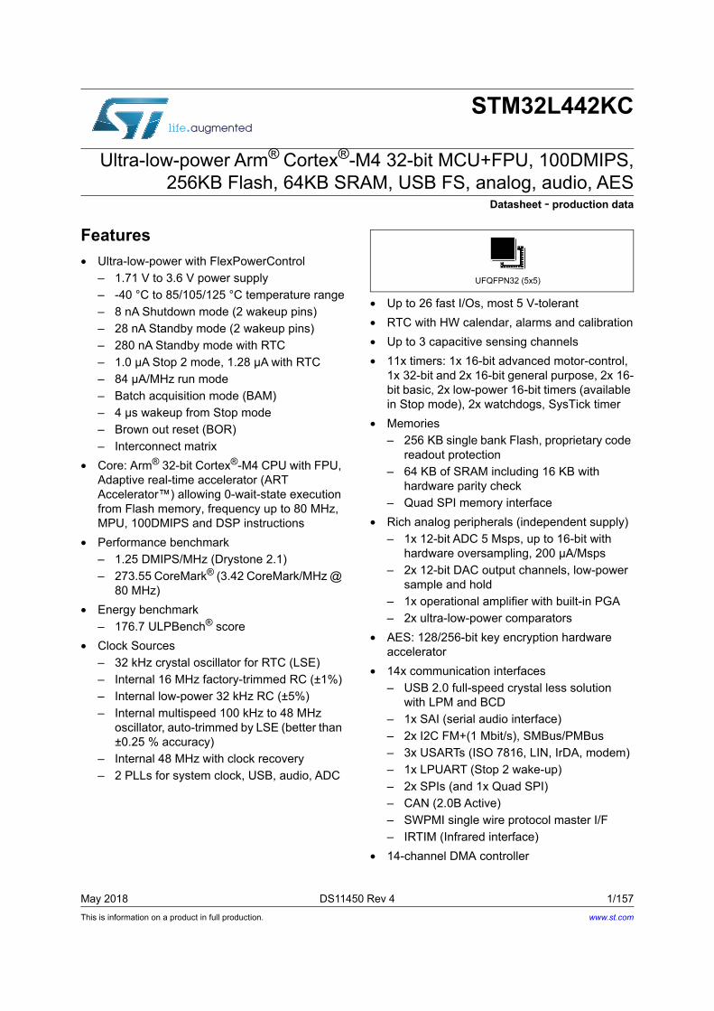
STM32L442KC
Ultra-low-power Arm® Cortex®-M4 32-bit MCU+FPU, 100DMIPS, 256KB Flash, 64KB SRAM, USB FS, analog, audio, AES
Datasheet - production data
Features
• Ultra-low-power with FlexPowerControl
– 1.71 V to 3.6 V power supply
– -40 °C to 85/105/125 °C temperature range
– 8 nA Shutdown mode (2 wakeup pins)
– 28 nA Standby mode (2 wakeup pins)
– 280 nA Standby mode with RTC
– 1.0 µA Stop 2 mode, 1.28 µA with RTC
– 84 µA/MHz run mode
– Batch acquisition mode (BAM)
– 4 µs wakeup from Stop mode
– Brown out reset (BOR)
– Interconnect matrix
• Core: Arm® 32-bit Cortex®-M4 CPU with FPU, Adaptive real-time accelerator (ART Accelerator™) allowing 0-wait-state execution from Flash memory, frequency up to 80 MHz, MPU, 100DMIPS and DSP instructions
• Performance benchmark
– 1.25 DMIPS/MHz (Drystone 2.1)
– 273.55 CoreMark® (3.42 CoreMark/MHz @ 80 MHz)
• Energy benchmark
– 176.7 ULPBench® score
• Clock Sources
– 32 kHz crystal oscillator for RTC (LSE)
– Internal 16 MHz factory-trimmed RC (±1%)
– Internal low-power 32 kHz RC (±5%)
– Internal multispeed 100 kHz to 48 MHz oscillator, auto-trimmed by LSE (better than ±0.25 % accuracy)
– Internal 48 MHz with clock recovery
– 2 PLLs for system clock, USB, audio, ADC
• Up to 26 fast I/Os, most 5 V-tolerant
• RTC with HW calendar, alarms and calibration
• Up to 3 capacitive sensing channels
• 11x timers: 1x 16-bit advanced motor-control, 1x 32-bit and 2x 16-bit general purpose, 2x 16-bit basic, 2x low-power 16-bit timers (available in Stop mode), 2x watchdogs, SysTick timer
• Memories
– 256 KB single bank Flash, proprietary code readout protection
– 64 KB of SRAM including 16 KB with hardware parity check
– Quad SPI memory interface
• Rich analog peripherals (independent supply)
– 1x 12-bit ADC 5 Msps, up to 16-bit with hardware oversampling, 200 µA/Msps
– 2x 12-bit DAC output channels, low-power sample and hold
– 1x operational amplifier with built-in PGA
– 2x ultra-low-power comparators
• AES: 128/256-bit key encryption hardware accelerator
• 14x communication interfaces
– USB 2.0 full-speed crystal less solution with LPM and BCD
– 1x SAI (serial audio interface)
– 2x I2C FM+(1 Mbit/s), SMBus/PMBus
– 3x USARTs (ISO 7816, LIN, IrDA, modem)
– 1x LPUART (Stop 2 wake-up)
– 2x SPIs (and 1x Quad SPI)
– CAN (2.0B Active)
– SWPMI single wire protocol master I/F
– IRTIM (Infrared interface)
• 14-channel DMA controller
UFQFPN32 (5x5)
www.st.com

STM32L442KC
2/157 DS11450 Rev 4
• True random number generator
• CRC calculation unit, 96-bit unique ID
• Development support: serial wire debug (SWD), JTAG, Embedded Trace Macrocell™
• All packages are ECOPACK2® compliant
DS11450 Rev 4 3/157
STM32L442KC Contents
6
Contents
1 Introduction . . . . . . . . . . . . . . . . . . . . . . . . . . . . . . . . . . . . . . . . . . . . . . . 10
2 Description . . . . . . . . . . . . . . . . . . . . . . . . . . . . . . . . . . . . . . . . . . . . . . . . 11
3 Functional overview . . . . . . . . . . . . . . . . . . . . . . . . . . . . . . . . . . . . . . . . 14
3.1 Arm® Cortex®-M4 core with FPU . . . . . . . . . . . . . . . . . . . . . . . . . . . . . . . 14
3.2 Adaptive real-time memory accelerator (ART Accelerator™) . . . . . . . . . 14
3.3 Memory protection unit . . . . . . . . . . . . . . . . . . . . . . . . . . . . . . . . . . . . . . . 14
3.4 Embedded Flash memory . . . . . . . . . . . . . . . . . . . . . . . . . . . . . . . . . . . . 15
3.5 Embedded SRAM . . . . . . . . . . . . . . . . . . . . . . . . . . . . . . . . . . . . . . . . . . . 16
3.6 Firewall . . . . . . . . . . . . . . . . . . . . . . . . . . . . . . . . . . . . . . . . . . . . . . . . . . . 16
3.7 Boot modes . . . . . . . . . . . . . . . . . . . . . . . . . . . . . . . . . . . . . . . . . . . . . . . 17
3.8 Cyclic redundancy check calculation unit (CRC) . . . . . . . . . . . . . . . . . . . 17
3.9 Power supply management . . . . . . . . . . . . . . . . . . . . . . . . . . . . . . . . . . . 17
3.9.1 Power supply schemes . . . . . . . . . . . . . . . . . . . . . . . . . . . . . . . . . . . . . 17
3.9.2 Power supply supervisor . . . . . . . . . . . . . . . . . . . . . . . . . . . . . . . . . . . . 19
3.9.3 Voltage regulator . . . . . . . . . . . . . . . . . . . . . . . . . . . . . . . . . . . . . . . . . . 20
3.9.4 Low-power modes . . . . . . . . . . . . . . . . . . . . . . . . . . . . . . . . . . . . . . . . . 20
3.9.5 Reset mode . . . . . . . . . . . . . . . . . . . . . . . . . . . . . . . . . . . . . . . . . . . . . . 28
3.10 Interconnect matrix . . . . . . . . . . . . . . . . . . . . . . . . . . . . . . . . . . . . . . . . . . 28
3.11 Clocks and startup . . . . . . . . . . . . . . . . . . . . . . . . . . . . . . . . . . . . . . . . . . 30
3.12 General-purpose inputs/outputs (GPIOs) . . . . . . . . . . . . . . . . . . . . . . . . . 33
3.13 Direct memory access controller (DMA) . . . . . . . . . . . . . . . . . . . . . . . . . . 33
3.14 Interrupts and events . . . . . . . . . . . . . . . . . . . . . . . . . . . . . . . . . . . . . . . . 34
3.14.1 Nested vectored interrupt controller (NVIC) . . . . . . . . . . . . . . . . . . . . . . 34
3.14.2 Extended interrupt/event controller (EXTI) . . . . . . . . . . . . . . . . . . . . . . 34
3.15 Analog to digital converter (ADC) . . . . . . . . . . . . . . . . . . . . . . . . . . . . . . . 35
3.15.1 Temperature sensor . . . . . . . . . . . . . . . . . . . . . . . . . . . . . . . . . . . . . . . . 35
3.15.2 Internal voltage reference (VREFINT) . . . . . . . . . . . . . . . . . . . . . . . . . . 36
3.16 Digital to analog converter (DAC) . . . . . . . . . . . . . . . . . . . . . . . . . . . . . . . 36
3.17 Comparators (COMP) . . . . . . . . . . . . . . . . . . . . . . . . . . . . . . . . . . . . . . . 37
3.18 Operational amplifier (OPAMP) . . . . . . . . . . . . . . . . . . . . . . . . . . . . . . . . 37
Contents STM32L442KC
4/157 DS11450 Rev 4
3.19 Touch sensing controller (TSC) . . . . . . . . . . . . . . . . . . . . . . . . . . . . . . . . 37
3.20 Random number generator (RNG) . . . . . . . . . . . . . . . . . . . . . . . . . . . . . . 38
3.21 Advanced encryption standard hardware accelerator (AES) . . . . . . . . . . 38
3.22 Timers and watchdogs . . . . . . . . . . . . . . . . . . . . . . . . . . . . . . . . . . . . . . . 39
3.22.1 Advanced-control timer (TIM1) . . . . . . . . . . . . . . . . . . . . . . . . . . . . . . . 40
3.22.2 General-purpose timers (TIM2, TIM15, TIM16) . . . . . . . . . . . . . . . . . . . 41
3.22.3 Basic timers (TIM6 and TIM7) . . . . . . . . . . . . . . . . . . . . . . . . . . . . . . . . 41
3.22.4 Low-power timer (LPTIM1 and LPTIM2) . . . . . . . . . . . . . . . . . . . . . . . . 41
3.22.5 Infrared interface (IRTIM) . . . . . . . . . . . . . . . . . . . . . . . . . . . . . . . . . . . 42
3.22.6 Independent watchdog (IWDG) . . . . . . . . . . . . . . . . . . . . . . . . . . . . . . . 42
3.22.7 System window watchdog (WWDG) . . . . . . . . . . . . . . . . . . . . . . . . . . . 42
3.22.8 SysTick timer . . . . . . . . . . . . . . . . . . . . . . . . . . . . . . . . . . . . . . . . . . . . . 42
3.23 Real-time clock (RTC) and backup registers . . . . . . . . . . . . . . . . . . . . . . 43
3.24 Inter-integrated circuit interface (I2C) . . . . . . . . . . . . . . . . . . . . . . . . . . . . 44
3.25 Universal synchronous/asynchronous receiver transmitter (USART) . . . 45
3.26 Low-power universal asynchronous receiver transmitter (LPUART) . . . . 46
3.27 Serial peripheral interface (SPI) . . . . . . . . . . . . . . . . . . . . . . . . . . . . . . . . 47
3.28 Serial audio interfaces (SAI) . . . . . . . . . . . . . . . . . . . . . . . . . . . . . . . . . . . 47
3.29 Single wire protocol master interface (SWPMI) . . . . . . . . . . . . . . . . . . . . 48
3.30 Controller area network (CAN) . . . . . . . . . . . . . . . . . . . . . . . . . . . . . . . . . 48
3.31 Universal serial bus (USB) . . . . . . . . . . . . . . . . . . . . . . . . . . . . . . . . . . . . 49
3.32 Clock recovery system (CRS) . . . . . . . . . . . . . . . . . . . . . . . . . . . . . . . . . 49
3.33 Quad SPI memory interface (QUADSPI) . . . . . . . . . . . . . . . . . . . . . . . . . 50
3.34 Development support . . . . . . . . . . . . . . . . . . . . . . . . . . . . . . . . . . . . . . . . 51
3.34.1 Serial wire JTAG debug port (SWJ-DP) . . . . . . . . . . . . . . . . . . . . . . . . . 51
3.34.2 Embedded Trace Macrocell™ . . . . . . . . . . . . . . . . . . . . . . . . . . . . . . . . 51
4 Pinouts and pin description . . . . . . . . . . . . . . . . . . . . . . . . . . . . . . . . . . 52
5 Memory mapping . . . . . . . . . . . . . . . . . . . . . . . . . . . . . . . . . . . . . . . . . . . 60
6 Electrical characteristics . . . . . . . . . . . . . . . . . . . . . . . . . . . . . . . . . . . . 64
6.1 Parameter conditions . . . . . . . . . . . . . . . . . . . . . . . . . . . . . . . . . . . . . . . . 64
6.1.1 Minimum and maximum values . . . . . . . . . . . . . . . . . . . . . . . . . . . . . . . 64
6.1.2 Typical values . . . . . . . . . . . . . . . . . . . . . . . . . . . . . . . . . . . . . . . . . . . . 64
DS11450 Rev 4 5/157
STM32L442KC Contents
6
6.1.3 Typical curves . . . . . . . . . . . . . . . . . . . . . . . . . . . . . . . . . . . . . . . . . . . . 64
6.1.4 Loading capacitor . . . . . . . . . . . . . . . . . . . . . . . . . . . . . . . . . . . . . . . . . 64
6.1.5 Pin input voltage . . . . . . . . . . . . . . . . . . . . . . . . . . . . . . . . . . . . . . . . . . 64
6.1.6 Power supply scheme . . . . . . . . . . . . . . . . . . . . . . . . . . . . . . . . . . . . . . 65
6.1.7 Current consumption measurement . . . . . . . . . . . . . . . . . . . . . . . . . . . 66
6.2 Absolute maximum ratings . . . . . . . . . . . . . . . . . . . . . . . . . . . . . . . . . . . . 66
6.3 Operating conditions . . . . . . . . . . . . . . . . . . . . . . . . . . . . . . . . . . . . . . . . 68
6.3.1 General operating conditions . . . . . . . . . . . . . . . . . . . . . . . . . . . . . . . . . 68
6.3.2 Operating conditions at power-up / power-down . . . . . . . . . . . . . . . . . . 69
6.3.3 Embedded reset and power control block characteristics . . . . . . . . . . . 69
6.3.4 Embedded voltage reference . . . . . . . . . . . . . . . . . . . . . . . . . . . . . . . . . 71
6.3.5 Supply current characteristics . . . . . . . . . . . . . . . . . . . . . . . . . . . . . . . . 73
6.3.6 Wakeup time from low-power modes and voltage scaling transition times . . . . . . . . . . . . . . . . . . . . . . . . . . . . . . . . . . . . . . . . . . . . 90
6.3.7 External clock source characteristics . . . . . . . . . . . . . . . . . . . . . . . . . . . 93
6.3.8 Internal clock source characteristics . . . . . . . . . . . . . . . . . . . . . . . . . . . 96
6.3.9 PLL characteristics . . . . . . . . . . . . . . . . . . . . . . . . . . . . . . . . . . . . . . . . 103
6.3.10 Flash memory characteristics . . . . . . . . . . . . . . . . . . . . . . . . . . . . . . . 104
6.3.11 EMC characteristics . . . . . . . . . . . . . . . . . . . . . . . . . . . . . . . . . . . . . . . 105
6.3.12 Electrical sensitivity characteristics . . . . . . . . . . . . . . . . . . . . . . . . . . . 106
6.3.13 I/O current injection characteristics . . . . . . . . . . . . . . . . . . . . . . . . . . . 107
6.3.14 I/O port characteristics . . . . . . . . . . . . . . . . . . . . . . . . . . . . . . . . . . . . . 108
6.3.15 NRST pin characteristics . . . . . . . . . . . . . . . . . . . . . . . . . . . . . . . . . . . 113
6.3.16 Extended interrupt and event controller input (EXTI) characteristics . . 114
6.3.17 Analog switches booster . . . . . . . . . . . . . . . . . . . . . . . . . . . . . . . . . . . 114
6.3.18 Analog-to-Digital converter characteristics . . . . . . . . . . . . . . . . . . . . . 115
6.3.19 Digital-to-Analog converter characteristics . . . . . . . . . . . . . . . . . . . . . 128
6.3.20 Comparator characteristics . . . . . . . . . . . . . . . . . . . . . . . . . . . . . . . . . 133
6.3.21 Operational amplifiers characteristics . . . . . . . . . . . . . . . . . . . . . . . . . 134
6.3.22 Temperature sensor characteristics . . . . . . . . . . . . . . . . . . . . . . . . . . . 137
6.3.23 Timer characteristics . . . . . . . . . . . . . . . . . . . . . . . . . . . . . . . . . . . . . . 137
6.3.24 Communication interfaces characteristics . . . . . . . . . . . . . . . . . . . . . . 139
7 Package information . . . . . . . . . . . . . . . . . . . . . . . . . . . . . . . . . . . . . . . 150
7.1 UFQFPN32 package information . . . . . . . . . . . . . . . . . . . . . . . . . . . . . . 150
7.2 Thermal characteristics . . . . . . . . . . . . . . . . . . . . . . . . . . . . . . . . . . . . . 153
7.2.1 Reference document . . . . . . . . . . . . . . . . . . . . . . . . . . . . . . . . . . . . . . 153
Contents STM32L442KC
6/157 DS11450 Rev 4
8 Ordering information . . . . . . . . . . . . . . . . . . . . . . . . . . . . . . . . . . . . . . 154
9 Revision history . . . . . . . . . . . . . . . . . . . . . . . . . . . . . . . . . . . . . . . . . . 155
DS11450 Rev 4 7/157
STM32L442KC List of tables
8
List of tables
Table 1. STM32L442KC family device features and peripheral counts . . . . . . . . . . . . . . . . . . . . . . 11Table 2. Access status versus readout protection level and execution modes. . . . . . . . . . . . . . . . . 15Table 3. STM32L442KC modes overview . . . . . . . . . . . . . . . . . . . . . . . . . . . . . . . . . . . . . . . . . . . . 21Table 4. Functionalities depending on the working mode. . . . . . . . . . . . . . . . . . . . . . . . . . . . . . . . . 26Table 5. STM32L442KC peripherals interconnect matrix . . . . . . . . . . . . . . . . . . . . . . . . . . . . . . . . . 29Table 6. DMA implementation . . . . . . . . . . . . . . . . . . . . . . . . . . . . . . . . . . . . . . . . . . . . . . . . . . . . . 33Table 7. Temperature sensor calibration values. . . . . . . . . . . . . . . . . . . . . . . . . . . . . . . . . . . . . . . . 36Table 8. Internal voltage reference calibration values . . . . . . . . . . . . . . . . . . . . . . . . . . . . . . . . . . . 36Table 9. Timer feature comparison. . . . . . . . . . . . . . . . . . . . . . . . . . . . . . . . . . . . . . . . . . . . . . . . . . 39Table 10. I2C implementation. . . . . . . . . . . . . . . . . . . . . . . . . . . . . . . . . . . . . . . . . . . . . . . . . . . . . . . 44Table 11. STM32L442KC USART/LPUART features. . . . . . . . . . . . . . . . . . . . . . . . . . . . . . . . . . . . . 45Table 12. SAI implementation. . . . . . . . . . . . . . . . . . . . . . . . . . . . . . . . . . . . . . . . . . . . . . . . . . . . . . . 48Table 13. Legend/abbreviations used in the pinout table . . . . . . . . . . . . . . . . . . . . . . . . . . . . . . . . . . 52Table 14. STM32L442KC pin definitions . . . . . . . . . . . . . . . . . . . . . . . . . . . . . . . . . . . . . . . . . . . . . . 53Table 15. Alternate function AF0 to AF7. . . . . . . . . . . . . . . . . . . . . . . . . . . . . . . . . . . . . . . . . . . . . . . 56Table 16. Alternate function AF8 to AF15. . . . . . . . . . . . . . . . . . . . . . . . . . . . . . . . . . . . . . . . . . . . . . 58Table 17. STM32L442KC memory map and peripheral register boundary addresses. . . . . . . . . . . . 61Table 18. Voltage characteristics . . . . . . . . . . . . . . . . . . . . . . . . . . . . . . . . . . . . . . . . . . . . . . . . . . . . 66Table 19. Current characteristics . . . . . . . . . . . . . . . . . . . . . . . . . . . . . . . . . . . . . . . . . . . . . . . . . . . . 67Table 20. Thermal characteristics. . . . . . . . . . . . . . . . . . . . . . . . . . . . . . . . . . . . . . . . . . . . . . . . . . . . 67Table 21. General operating conditions . . . . . . . . . . . . . . . . . . . . . . . . . . . . . . . . . . . . . . . . . . . . . . . 68Table 22. Operating conditions at power-up / power-down . . . . . . . . . . . . . . . . . . . . . . . . . . . . . . . . 69Table 23. Embedded reset and power control block characteristics. . . . . . . . . . . . . . . . . . . . . . . . . . 69Table 24. Embedded internal voltage reference. . . . . . . . . . . . . . . . . . . . . . . . . . . . . . . . . . . . . . . . . 71Table 25. Current consumption in Run and Low-power run modes, code with data processing
running from Flash, ART enable (Cache ON Prefetch OFF) . . . . . . . . . . . . . . . . . . . . . . . 74Table 26. Current consumption in Run and Low-power run modes, code with data processing
running from Flash, ART disable . . . . . . . . . . . . . . . . . . . . . . . . . . . . . . . . . . . . . . . . . . . . 75Table 27. Current consumption in Run and Low-power run modes, code with data processing
running from SRAM1 . . . . . . . . . . . . . . . . . . . . . . . . . . . . . . . . . . . . . . . . . . . . . . . . . . . . . 76Table 28. Typical current consumption in Run and Low-power run modes, with different codes
running from Flash, ART enable (Cache ON Prefetch OFF) . . . . . . . . . . . . . . . . . . . . . . . 77Table 29. Typical current consumption in Run and Low-power run modes, with different codes
running from Flash, ART disable . . . . . . . . . . . . . . . . . . . . . . . . . . . . . . . . . . . . . . . . . . . . 78Table 30. Typical current consumption in Run and Low-power run modes, with different codes
running from SRAM1 . . . . . . . . . . . . . . . . . . . . . . . . . . . . . . . . . . . . . . . . . . . . . . . . . . . . . 78Table 31. Current consumption in Sleep and Low-power sleep modes, Flash ON . . . . . . . . . . . . . . 79Table 32. Current consumption in Low-power sleep modes, Flash in power-down . . . . . . . . . . . . . . 80Table 33. Current consumption in Stop 2 mode . . . . . . . . . . . . . . . . . . . . . . . . . . . . . . . . . . . . . . . . . 80Table 34. Current consumption in Stop 1 mode . . . . . . . . . . . . . . . . . . . . . . . . . . . . . . . . . . . . . . . . . 82Table 35. Current consumption in Stop 0 . . . . . . . . . . . . . . . . . . . . . . . . . . . . . . . . . . . . . . . . . . . . . . 83Table 36. Current consumption in Standby mode . . . . . . . . . . . . . . . . . . . . . . . . . . . . . . . . . . . . . . . 84Table 37. Current consumption in Shutdown mode . . . . . . . . . . . . . . . . . . . . . . . . . . . . . . . . . . . . . . 85Table 38. Peripheral current consumption . . . . . . . . . . . . . . . . . . . . . . . . . . . . . . . . . . . . . . . . . . . . . 88Table 39. Low-power mode wakeup timings . . . . . . . . . . . . . . . . . . . . . . . . . . . . . . . . . . . . . . . . . . . 90Table 40. Regulator modes transition times . . . . . . . . . . . . . . . . . . . . . . . . . . . . . . . . . . . . . . . . . . . . 92Table 41. Wakeup time using USART/LPUART. . . . . . . . . . . . . . . . . . . . . . . . . . . . . . . . . . . . . . . . . 92Table 42. High-speed external user clock characteristics. . . . . . . . . . . . . . . . . . . . . . . . . . . . . . . . . . 93
List of tables STM32L442KC
8/157 DS11450 Rev 4
Table 43. Low-speed external user clock characteristics . . . . . . . . . . . . . . . . . . . . . . . . . . . . . . . . . . 94Table 44. LSE oscillator characteristics (fLSE = 32.768 kHz) . . . . . . . . . . . . . . . . . . . . . . . . . . . . . . . 95Table 45. HSI16 oscillator characteristics. . . . . . . . . . . . . . . . . . . . . . . . . . . . . . . . . . . . . . . . . . . . . . 96Table 46. MSI oscillator characteristics . . . . . . . . . . . . . . . . . . . . . . . . . . . . . . . . . . . . . . . . . . . . . . . . . . . . . . . .98Table 47. HSI48 oscillator characteristics. . . . . . . . . . . . . . . . . . . . . . . . . . . . . . . . . . . . . . . . . . . . . 101Table 48. LSI oscillator characteristics . . . . . . . . . . . . . . . . . . . . . . . . . . . . . . . . . . . . . . . . . . . . . . . 102Table 49. PLL, PLLSAI1 characteristics . . . . . . . . . . . . . . . . . . . . . . . . . . . . . . . . . . . . . . . . . . . . . . 103Table 50. Flash memory characteristics . . . . . . . . . . . . . . . . . . . . . . . . . . . . . . . . . . . . . . . . . . . . . . 104Table 51. Flash memory endurance and data retention . . . . . . . . . . . . . . . . . . . . . . . . . . . . . . . . . . 104Table 52. EMS characteristics . . . . . . . . . . . . . . . . . . . . . . . . . . . . . . . . . . . . . . . . . . . . . . . . . . . . . 105Table 53. EMI characteristics . . . . . . . . . . . . . . . . . . . . . . . . . . . . . . . . . . . . . . . . . . . . . . . . . . . . . . 106Table 54. ESD absolute maximum ratings . . . . . . . . . . . . . . . . . . . . . . . . . . . . . . . . . . . . . . . . . . . . 106Table 55. Electrical sensitivities . . . . . . . . . . . . . . . . . . . . . . . . . . . . . . . . . . . . . . . . . . . . . . . . . . . . 107Table 56. I/O current injection susceptibility . . . . . . . . . . . . . . . . . . . . . . . . . . . . . . . . . . . . . . . . . . . 107Table 57. I/O static characteristics . . . . . . . . . . . . . . . . . . . . . . . . . . . . . . . . . . . . . . . . . . . . . . . . . . 108Table 58. Output voltage characteristics . . . . . . . . . . . . . . . . . . . . . . . . . . . . . . . . . . . . . . . . . . . . . 110Table 59. I/O AC characteristics . . . . . . . . . . . . . . . . . . . . . . . . . . . . . . . . . . . . . . . . . . . . . . . . . . . . 111Table 60. NRST pin characteristics . . . . . . . . . . . . . . . . . . . . . . . . . . . . . . . . . . . . . . . . . . . . . . . . . 113Table 61. EXTI Input Characteristics . . . . . . . . . . . . . . . . . . . . . . . . . . . . . . . . . . . . . . . . . . . . . . . . 114Table 62. Analog switches booster characteristics . . . . . . . . . . . . . . . . . . . . . . . . . . . . . . . . . . . . . . 114Table 63. ADC characteristics . . . . . . . . . . . . . . . . . . . . . . . . . . . . . . . . . . . . . . . . . . . . . . . . . . . . 115Table 64. Maximum ADC RAIN . . . . . . . . . . . . . . . . . . . . . . . . . . . . . . . . . . . . . . . . . . . . . . . . . . . . 117Table 65. ADC accuracy - limited test conditions 1 . . . . . . . . . . . . . . . . . . . . . . . . . . . . . . . . . . . . . 119Table 66. ADC accuracy - limited test conditions 2 . . . . . . . . . . . . . . . . . . . . . . . . . . . . . . . . . . . . . 121Table 67. ADC accuracy - limited test conditions 3 . . . . . . . . . . . . . . . . . . . . . . . . . . . . . . . . . . . . . 123Table 68. ADC accuracy - limited test conditions 4 . . . . . . . . . . . . . . . . . . . . . . . . . . . . . . . . . . . . . 125Table 69. DAC characteristics . . . . . . . . . . . . . . . . . . . . . . . . . . . . . . . . . . . . . . . . . . . . . . . . . . . . . 128Table 70. DAC accuracy. . . . . . . . . . . . . . . . . . . . . . . . . . . . . . . . . . . . . . . . . . . . . . . . . . . . . . . . . . 131Table 71. COMP characteristics . . . . . . . . . . . . . . . . . . . . . . . . . . . . . . . . . . . . . . . . . . . . . . . . . . . . 133Table 72. OPAMP characteristics . . . . . . . . . . . . . . . . . . . . . . . . . . . . . . . . . . . . . . . . . . . . . . . . . . 134Table 73. TS characteristics . . . . . . . . . . . . . . . . . . . . . . . . . . . . . . . . . . . . . . . . . . . . . . . . . . . . . . . 137Table 74. TIMx characteristics . . . . . . . . . . . . . . . . . . . . . . . . . . . . . . . . . . . . . . . . . . . . . . . . . . . . . 138Table 75. IWDG min/max timeout period at 32 kHz (LSI). . . . . . . . . . . . . . . . . . . . . . . . . . . . . . . . . 138Table 76. WWDG min/max timeout value at 80 MHz (PCLK). . . . . . . . . . . . . . . . . . . . . . . . . . . . . . 138Table 77. I2C analog filter characteristics. . . . . . . . . . . . . . . . . . . . . . . . . . . . . . . . . . . . . . . . . . . . . 139Table 78. SPI characteristics . . . . . . . . . . . . . . . . . . . . . . . . . . . . . . . . . . . . . . . . . . . . . . . . . . . . . . 140Table 79. Quad SPI characteristics in SDR mode . . . . . . . . . . . . . . . . . . . . . . . . . . . . . . . . . . . . . . 143Table 80. QUADSPI characteristics in DDR mode . . . . . . . . . . . . . . . . . . . . . . . . . . . . . . . . . . . . . . 144Table 81. SAI characteristics . . . . . . . . . . . . . . . . . . . . . . . . . . . . . . . . . . . . . . . . . . . . . . . . . . . . . . 146Table 82. USB electrical characteristics . . . . . . . . . . . . . . . . . . . . . . . . . . . . . . . . . . . . . . . . . . . . . . 148Table 83. SWPMI electrical characteristics . . . . . . . . . . . . . . . . . . . . . . . . . . . . . . . . . . . . . . . . . . . 149Table 84. UFQFPN32 - 32-pin, 5x5 mm, 0.5 mm pitch ultra thin fine pitch quad flat
package mechanical data . . . . . . . . . . . . . . . . . . . . . . . . . . . . . . . . . . . . . . . . . . . . . . . . . 151Table 85. Package thermal characteristics . . . . . . . . . . . . . . . . . . . . . . . . . . . . . . . . . . . . . . . . . . . . 153Table 86. STM32L442KC ordering information scheme. . . . . . . . . . . . . . . . . . . . . . . . . . . . . . . . . . 154Table 87. Document revision history . . . . . . . . . . . . . . . . . . . . . . . . . . . . . . . . . . . . . . . . . . . . . . . . 155
DS11450 Rev 4 9/157
STM32L442KC List of figures
9
List of figures
Figure 1. STM32L442KC block diagram . . . . . . . . . . . . . . . . . . . . . . . . . . . . . . . . . . . . . . . . . . . . . . 13Figure 2. Power supply overview . . . . . . . . . . . . . . . . . . . . . . . . . . . . . . . . . . . . . . . . . . . . . . . . . . . . 18Figure 3. Power-up/down sequence . . . . . . . . . . . . . . . . . . . . . . . . . . . . . . . . . . . . . . . . . . . . . . . . . 19Figure 4. Clock tree . . . . . . . . . . . . . . . . . . . . . . . . . . . . . . . . . . . . . . . . . . . . . . . . . . . . . . . . . . . . . . 32Figure 5. STM32L442KC UFQFPN32 pinout(1) . . . . . . . . . . . . . . . . . . . . . . . . . . . . . . . . . . . . . . . . . 52Figure 6. STM32L442KC memory map . . . . . . . . . . . . . . . . . . . . . . . . . . . . . . . . . . . . . . . . . . . . . . . 60Figure 7. Pin loading conditions. . . . . . . . . . . . . . . . . . . . . . . . . . . . . . . . . . . . . . . . . . . . . . . . . . . . . 64Figure 8. Pin input voltage . . . . . . . . . . . . . . . . . . . . . . . . . . . . . . . . . . . . . . . . . . . . . . . . . . . . . . . . . 64Figure 9. Power supply scheme. . . . . . . . . . . . . . . . . . . . . . . . . . . . . . . . . . . . . . . . . . . . . . . . . . . . . 65Figure 10. Current consumption measurement scheme . . . . . . . . . . . . . . . . . . . . . . . . . . . . . . . . . . . 66Figure 11. VREFINT versus temperature . . . . . . . . . . . . . . . . . . . . . . . . . . . . . . . . . . . . . . . . . . . . . . 72Figure 12. High-speed external clock source AC timing diagram . . . . . . . . . . . . . . . . . . . . . . . . . . . . 93Figure 13. Low-speed external clock source AC timing diagram. . . . . . . . . . . . . . . . . . . . . . . . . . . . . 94Figure 14. Typical application with a 32.768 kHz crystal . . . . . . . . . . . . . . . . . . . . . . . . . . . . . . . . . . . 95Figure 15. HSI16 frequency versus temperature . . . . . . . . . . . . . . . . . . . . . . . . . . . . . . . . . . . . . . . . . 97Figure 16. Typical current consumption versus MSI frequency . . . . . . . . . . . . . . . . . . . . . . . . . . . . . 101Figure 17. HSI48 frequency versus temperature . . . . . . . . . . . . . . . . . . . . . . . . . . . . . . . . . . . . . . . . 102Figure 18. I/O input characteristics . . . . . . . . . . . . . . . . . . . . . . . . . . . . . . . . . . . . . . . . . . . . . . . . . . 109Figure 19. I/O AC characteristics definition(1) . . . . . . . . . . . . . . . . . . . . . . . . . . . . . . . . . . . . . . . . . . 113Figure 20. Recommended NRST pin protection . . . . . . . . . . . . . . . . . . . . . . . . . . . . . . . . . . . . . . . . 114Figure 21. ADC accuracy characteristics . . . . . . . . . . . . . . . . . . . . . . . . . . . . . . . . . . . . . . . . . . . . . . 126Figure 22. Typical connection diagram using the ADC . . . . . . . . . . . . . . . . . . . . . . . . . . . . . . . . . . . 127Figure 23. 12-bit buffered / non-buffered DAC. . . . . . . . . . . . . . . . . . . . . . . . . . . . . . . . . . . . . . . . . . 130Figure 24. SPI timing diagram - slave mode and CPHA = 0 . . . . . . . . . . . . . . . . . . . . . . . . . . . . . . . 141Figure 25. SPI timing diagram - slave mode and CPHA = 1 . . . . . . . . . . . . . . . . . . . . . . . . . . . . . . . 142Figure 26. SPI timing diagram - master mode . . . . . . . . . . . . . . . . . . . . . . . . . . . . . . . . . . . . . . . . . . 142Figure 27. Quad SPI timing diagram - SDR mode. . . . . . . . . . . . . . . . . . . . . . . . . . . . . . . . . . . . . . . 145Figure 28. Quad SPI timing diagram - DDR mode. . . . . . . . . . . . . . . . . . . . . . . . . . . . . . . . . . . . . . . 145Figure 29. SAI master timing waveforms . . . . . . . . . . . . . . . . . . . . . . . . . . . . . . . . . . . . . . . . . . . . . . 147Figure 30. SAI slave timing waveforms . . . . . . . . . . . . . . . . . . . . . . . . . . . . . . . . . . . . . . . . . . . . . . . 148Figure 31. UFQFPN32 - 32-pin, 5x5 mm, 0.5 mm pitch ultra thin fine pitch quad flat
package outline. . . . . . . . . . . . . . . . . . . . . . . . . . . . . . . . . . . . . . . . . . . . . . . . . . . . . . . . . 150Figure 32. UFQFPN32 - 32-pin, 5x5 mm, 0.5 mm pitch ultra thin fine pitch quad flat
package recommended footprint . . . . . . . . . . . . . . . . . . . . . . . . . . . . . . . . . . . . . . . . . . . 151Figure 33. UFQFPN32 marking (package top view) . . . . . . . . . . . . . . . . . . . . . . . . . . . . . . . . . . . . . 152
Introduction STM32L442KC
10/157 DS11450 Rev 4
1 Introduction
This datasheet provides the ordering information and mechanical device characteristics of the STM32L442KC microcontrollers.
This document should be read in conjunction with the STM32L43xxx/44xxx/45xxx/46xxx reference manual (RM0394). The reference manual is available from the STMicroelectronics website www.st.com.
For information on the Arm®(a) Cortex®-M4 core, please refer to the Cortex®-M4 Technical Reference Manual, available from the www.arm.com website.
a. Arm is a registered trademark of Arm Limited (or its subsidiaries) in the US and/or elsewhere.
DS11450 Rev 4 11/157
STM32L442KC Description
51
2 Description
The STM32L442KC devices are the ultra-low-power microcontrollers based on the high-performance Arm® Cortex®-M4 32-bit RISC core operating at a frequency of up to 80 MHz. The Cortex-M4 core features a Floating point unit (FPU) single precision which supports all Arm® single-precision data-processing instructions and data types. It also implements a full set of DSP instructions and a memory protection unit (MPU) which enhances application security.
The STM32L442KC devices embed high-speed memories (256 Kbyte of Flash memory, 64 Kbyte of SRAM), a Quad SPI flash memories interface and an extensive range of enhanced I/Os and peripherals connected to two APB buses, two AHB buses and a 32-bit multi-AHB bus matrix.
The STM32L442KC devices embed several protection mechanisms for embedded Flash memory and SRAM: readout protection, write protection, proprietary code readout protection and Firewall.
The devices offer a fast 12-bit ADC (5 Msps), two comparators, one operational amplifier, two DAC channels, a low-power RTC, one general-purpose 32-bit timer, one 16-bit PWM timer dedicated to motor control, four general-purpose 16-bit timers, and two 16-bit low-power timers.
In addition, up to 3 capacitive sensing channels are available.
They also feature standard and advanced communication interfaces.
• Two I2Cs
• Two SPIs
• Two USARTs and one Low-Power UART.
• One SAI (Serial Audio Interfaces)
• One CAN
• One USB full-speed device crystal less
• One SWPMI (Single Wire Protocol Master Interface)
The STM32L442KC devices embed AES hardware accelerator.
The STM32L442KC operates in the -40 to +85 °C (+105 °C junction), -40 to +105 °C (+125 °C junction) and -40 to +125 °C (+130 °C junction) temperature ranges from a 1.71 to 3.6 V power supply. A comprehensive set of power-saving modes allows the design of low-power applications.
Some independent power supplies are supported: analog independent supply input for ADC, DAC, OPAMP and comparators
The STM32L442KC family offers a single 32-pin package.
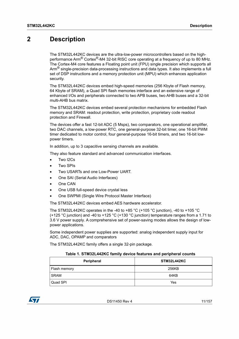
Table 1. STM32L442KC family device features and peripheral counts
Peripheral STM32L442KC
Flash memory 256KB
SRAM 64KB
Quad SPI Yes
Description STM32L442KC
12/157 DS11450 Rev 4
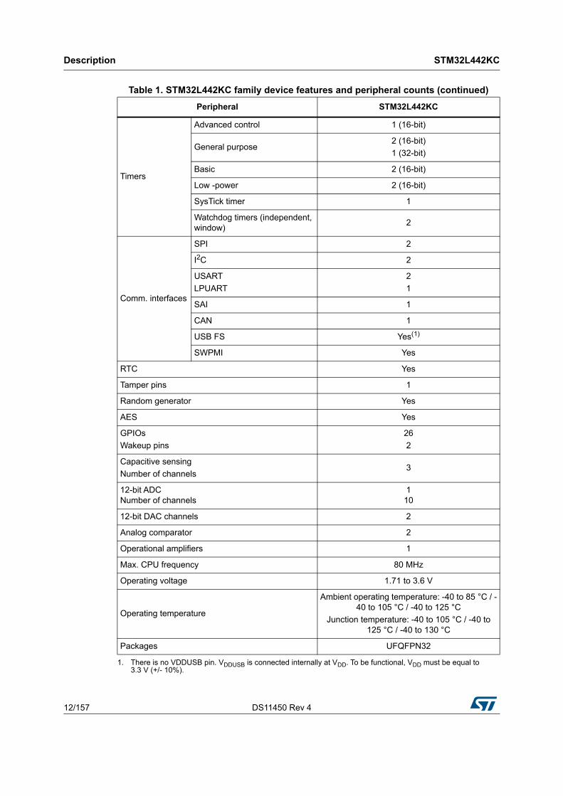
Timers
Advanced control 1 (16-bit)
General purpose2 (16-bit)
1 (32-bit)
Basic 2 (16-bit)
Low -power 2 (16-bit)
SysTick timer 1
Watchdog timers (independent, window)
2
Comm. interfaces
SPI 2
I2C 2
USART
LPUART
2
1
SAI 1
CAN 1
USB FS Yes(1)
SWPMI Yes
RTC Yes
Tamper pins 1
Random generator Yes
AES Yes
GPIOs
Wakeup pins
26
2
Capacitive sensing
Number of channels3
12-bit ADC Number of channels
110
12-bit DAC channels 2
Analog comparator 2
Operational amplifiers 1
Max. CPU frequency 80 MHz
Operating voltage 1.71 to 3.6 V
Operating temperature
Ambient operating temperature: -40 to 85 °C / -40 to 105 °C / -40 to 125 °C
Junction temperature: -40 to 105 °C / -40 to 125 °C / -40 to 130 °C
Packages UFQFPN32
1. There is no VDDUSB pin. VDDUSB is connected internally at VDD. To be functional, VDD must be equal to 3.3 V (+/- 10%).
Table 1. STM32L442KC family device features and peripheral counts (continued)
Peripheral STM32L442KC
DS11450 Rev 4 13/157
STM32L442KC Description
51
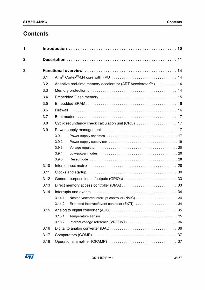
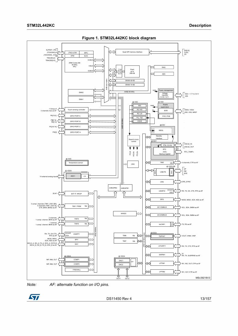
Figure 1. STM32L442KC block diagram
Note: AF: alternate function on I/O pins.
MSv39218V3
Flashup to
256 KB
USB FS
GPIO PORT A
AHB/APB2
PA[15:0]
AP
B2
60M
Hz
AP
B1
30
MH
z
OUT1
ITF
WWDG
OSC32_IN
OSC32_OUT
JTAG & SW
ARM Cortex-M480 MHz
FPU
NVICETM
MPU
DMA2
AR
T A
CC
EL/
CA
CH
E
RNG
@ VDDA
BOR
Supplysupervision
PVD, PVM
Int
reset
XTAL 32 kHz
M AN A G T
RTC
FCLK
Standbyinterface
IWDG
@VBAT
@ VDD
@VDD
AWU
Reset & clockcontrol
PC
LKx
Voltageregulator
3.3 to 1.2 V
VDD Power management
@ VDD
RTC_TAMPxBackup register
AH
B b
us-m
atrix
DAC1
DAC2
TIM6
TIM7
TIM2
D-BUS
SRAM 48 KB
AP
B1
80 M
Hz
(max
)
SRAM 16 KB
I-BUS
S-BUS
DMA1
PB[7:3],PB[1:0]
PC[15:14]
GPIO PORT B
GPIO PORT C
GPIO PORT H
OUT2
16b
16b
32b 4 channels, ETR as AF
AHB/APB1
HC
LKx
10 external analog inputs
U S AR T 2 M B p sTemperature sensor
@ VDDA
Touch sensing controller1 Group of3 channels max as AF
RC HSI
RC LSI
PLL 1&2
MSI
Quad SPI memory interfaceD0[3:0],CLK0,CS
@ VDDUSB
COMP1INP, INM, OUT
COMP2INP, INM, OUT
@ VDDA
FIFO
PH
Y
AH
B1
80 M
Hz
CRC
AP
B2
80M
Hz
AHB2 80 MHz
FIREWALL
@ VDD
DPDM
VDD = 1.71 to 3.6 VVSS
TRACECLKTRACED[3:0]
NJTRST, JTDI,JTCK/SWCLK
JTDO/SWD, JTDO
ITFADC1
NOE
HSI48
LPTIM2 IN1, OUT, ETR as AF
LPTIM1 IN1, IN2, OUT, ETR as AF
SWPMI1 IORX, TX, SUSPEND as AF
LPUART1 RX, TX, CTS, RTS as AF
VOUT, VINM, VINPOpAmp1
@VDDA
FIFO TX, RX as AFbxCAN1
SCL, SDA, SMBA as AFI2C3/SMBUS
I2C1/SMBUS SCL, SDA, SMBA as AF
MOSI, MISO, SCK, NSS as AFSPI3
USART2 RX, TX, CK, CTS, RTS as AFsmcard
IrDA
CRS CRS_SYNC
VDDA, VSSAVDD, VSS, NRST
PH[3]
EXT IT. WKUP26 AF
TIM1 / PWM3 compl. channels (TIM1_CH[1:3]N),
4 channels (TIM1_CH[1:4]),ETR, BKIN, BKIN2 as AF
16b
TIM152 channels,
1 compl. channel, BKIN as AF16b
TIM16 16b1 channel,
1 compl. channel, BKIN as AF
USART1RX, TX, CK,CTS, RTS as AF
smcardIrDA
SPI1MOSI, MISO,SCK, NSS as AF
SAI1MCLK_A, SD_A, FS_A, SCK_A, EXTCLKMCLK_B, SD_B, FS_B, SCK_B as AF
AES
Functional overview STM32L442KC
14/157 DS11450 Rev 4
3 Functional overview
3.1 Arm® Cortex®-M4 core with FPU
The Arm® Cortex®-M4 with FPU processor is the latest generation of Arm® processors for embedded systems. It was developed to provide a low-cost platform that meets the needs of MCU implementation, with a reduced pin count and low-power consumption, while delivering outstanding computational performance and an advanced response to interrupts.
The Arm® Cortex®-M4 with FPU 32-bit RISC processor features exceptional code-efficiency, delivering the high-performance expected from an Arm® core in the memory size usually associated with 8- and 16-bit devices.
The processor supports a set of DSP instructions which allow efficient signal processing and complex algorithm execution.
Its single precision FPU speeds up software development by using metalanguage development tools, while avoiding saturation.
With its embedded Arm® core, the STM32L442KC family is compatible with all Arm® tools and software.
Figure 1 shows the general block diagram of the STM32L442KC family devices.
3.2 Adaptive real-time memory accelerator (ART Accelerator™)
The ART Accelerator™ is a memory accelerator which is optimized for STM32 industry-standard Arm® Cortex®-M4 processors. It balances the inherent performance advantage of the Arm® Cortex®-M4 over Flash memory technologies, which normally requires the processor to wait for the Flash memory at higher frequencies.
To release the processor near 100 DMIPS performance at 80MHz, the accelerator implements an instruction prefetch queue and branch cache, which increases program execution speed from the 64-bit Flash memory. Based on CoreMark benchmark, the performance achieved thanks to the ART accelerator is equivalent to 0 wait state program execution from Flash memory at a CPU frequency up to 80 MHz.
3.3 Memory protection unit
The memory protection unit (MPU) is used to manage the CPU accesses to memory to prevent one task to accidentally corrupt the memory or resources used by any other active task. This memory area is organized into up to 8 protected areas that can in turn be divided up into 8 subareas. The protection area sizes are between 32 bytes and the whole 4 gigabytes of addressable memory.
The MPU is especially helpful for applications where some critical or certified code has to be protected against the misbehavior of other tasks. It is usually managed by an RTOS (real-time operating system). If a program accesses a memory location that is prohibited by the MPU, the RTOS can detect it and take action. In an RTOS environment, the kernel can dynamically update the MPU area setting, based on the process to be executed.
The MPU is optional and can be bypassed for applications that do not need it.
DS11450 Rev 4 15/157
STM32L442KC Functional overview
51
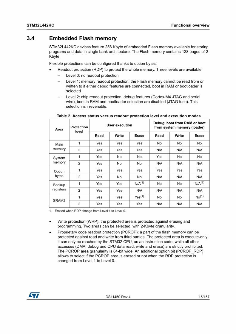
3.4 Embedded Flash memory
STM32L442KC devices feature 256 Kbyte of embedded Flash memory available for storing programs and data in single bank architecture. The Flash memory contains 128 pages of 2 Kbyte.
Flexible protections can be configured thanks to option bytes:
• Readout protection (RDP) to protect the whole memory. Three levels are available:
– Level 0: no readout protection
– Level 1: memory readout protection: the Flash memory cannot be read from or written to if either debug features are connected, boot in RAM or bootloader is selected
– Level 2: chip readout protection: debug features (Cortex-M4 JTAG and serial wire), boot in RAM and bootloader selection are disabled (JTAG fuse). This selection is irreversible.
• Write protection (WRP): the protected area is protected against erasing and programming. Two areas can be selected, with 2-Kbyte granularity.
• Proprietary code readout protection (PCROP): a part of the flash memory can be protected against read and write from third parties. The protected area is execute-only: it can only be reached by the STM32 CPU, as an instruction code, while all other accesses (DMA, debug and CPU data read, write and erase) are strictly prohibited. The PCROP area granularity is 64-bit wide. An additional option bit (PCROP_RDP) allows to select if the PCROP area is erased or not when the RDP protection is changed from Level 1 to Level 0.
Table 2. Access status versus readout protection level and execution modes
AreaProtection
level
User executionDebug, boot from RAM or boot from system memory (loader)
Read Write Erase Read Write Erase
Main memory
1 Yes Yes Yes No No No
2 Yes Yes Yes N/A N/A N/A
System memory
1 Yes No No Yes No No
2 Yes No No N/A N/A N/A
Option bytes
1 Yes Yes Yes Yes Yes Yes
2 Yes No No N/A N/A N/A
Backup registers
1 Yes Yes N/A(1)
1. Erased when RDP change from Level 1 to Level 0.
No No N/A(1)
2 Yes Yes N/A N/A N/A N/A
SRAM21 Yes Yes Yes(1) No No No(1)
2 Yes Yes Yes N/A N/A N/A
Functional overview STM32L442KC
16/157 DS11450 Rev 4
The whole non-volatile memory embeds the error correction code (ECC) feature supporting:
• single error detection and correction
• double error detection.
• The address of the ECC fail can be read in the ECC register
3.5 Embedded SRAM
STM32L442KC devices feature 64 Kbyte of embedded SRAM. This SRAM is split into two blocks:
• 48 Kbyte mapped at address 0x2000 0000 (SRAM1)
• 16 Kbyte located at address 0x1000 0000 with hardware parity check (SRAM2).
This memory is also mapped at address 0x2000 C000, offering a contiguous address space with the SRAM1 (16 Kbyte aliased by bit band)
This block is accessed through the ICode/DCode buses for maximum performance. These 16 Kbyte SRAM can also be retained in Standby mode.
The SRAM2 can be write-protected with 1 Kbyte granularity.
The memory can be accessed in read/write at CPU clock speed with 0 wait states.
3.6 Firewall
The device embeds a Firewall which protects code sensitive and secure data from any access performed by a code executed outside of the protected areas.
Each illegal access generates a reset which kills immediately the detected intrusion.
The Firewall main features are the following:
• Three segments can be protected and defined thanks to the Firewall registers:
– Code segment (located in Flash or SRAM1 if defined as executable protected area)
– Non-volatile data segment (located in Flash)
– Volatile data segment (located in SRAM1)
• The start address and the length of each segments are configurable:
– Code segment: up to 1024 Kbyte with granularity of 256 bytes
– Non-volatile data segment: up to 1024 Kbyte with granularity of 256 bytes
– Volatile data segment: up to 48 Kbyte with a granularity of 64 bytes
• Specific mechanism implemented to open the Firewall to get access to the protected areas (call gate entry sequence)
• Volatile data segment can be shared or not with the non-protected code
• Volatile data segment can be executed or not depending on the Firewall configuration
The Flash readout protection must be set to level 2 in order to reach the expected level of protection.
DS11450 Rev 4 17/157
STM32L442KC Functional overview
51
3.7 Boot modes
At startup, BOOT0 pin or nSWBOOT0 option bit, and BOOT1 option bit are used to select one of three boot options:
• Boot from user Flash
• Boot from system memory
• Boot from embedded SRAM
BOOT0 value may come from the PH3-BOOT0 pin or from an option bit depending on the value of a user option bit to free the GPIO pad if needed.
A Flash empty check mechanism is implemented to force the boot from system flash if the first flash memory location is not programmed and if the boot selection is configured to boot from main flash.
The boot loader is located in system memory. It is used to reprogram the Flash memory by using USART, I2C, SPI or USB FS in Device mode through DFU (device firmware upgrade).
3.8 Cyclic redundancy check calculation unit (CRC)
The CRC (cyclic redundancy check) calculation unit is used to get a CRC code using a configurable generator polynomial value and size.
Among other applications, CRC-based techniques are used to verify data transmission or storage integrity. In the scope of the EN/IEC 60335-1 standard, they offer a means of verifying the Flash memory integrity. The CRC calculation unit helps compute a signature of the software during runtime, to be compared with a reference signature generated at link-time and stored at a given memory location.
3.9 Power supply management
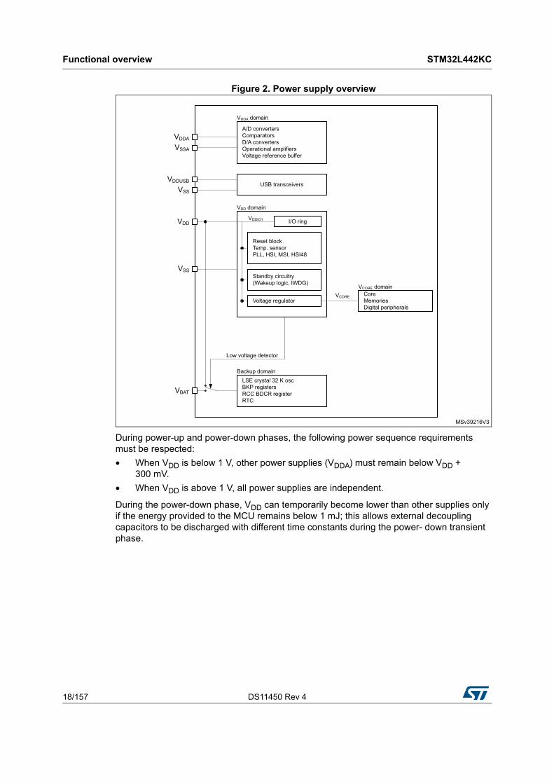
3.9.1 Power supply schemes
• VDD = 1.71 to 3.6 V: external power supply for I/Os (VDDIO1), the internal regulator and the system analog such as reset, power management and internal clocks. It is provided externally through VDD pins.
• VDDA = 1.62 V (ADCs/COMPs) / 1.8 (DAC/OPAMP) to 3.6 V: external analog power supply for ADCs, DAC, OPAMPs, Comparators and Voltage reference buffer. The VDDA voltage level is independent from the VDD voltage.
Note: When the functions supplied by VDDA or VDDUSB are not used, these supplies should preferably be shorted to VDD.
Note: If these supplies are tied to ground, the I/Os supplied by these power supplies are not 5 V tolerant (refer to Table 18: Voltage characteristics).
Note: VDDIOx is the I/Os general purpose digital functions supply. VDDIOx represents VDDIO1, with VDDIO1 = VDD.
Functional overview STM32L442KC
18/157 DS11450 Rev 4
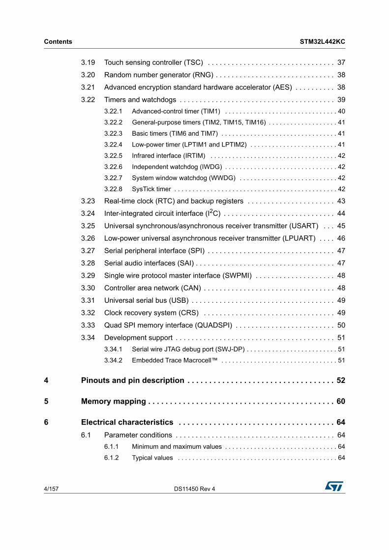
Figure 2. Power supply overview
During power-up and power-down phases, the following power sequence requirements must be respected:
• When VDD is below 1 V, other power supplies (VDDA) must remain below VDD + 300 mV.
• When VDD is above 1 V, all power supplies are independent.
During the power-down phase, VDD can temporarily become lower than other supplies only if the energy provided to the MCU remains below 1 mJ; this allows external decoupling capacitors to be discharged with different time constants during the power- down transient phase.
MSv39216V3
Low voltage detector
VDDA
VDDA domain
VSS
VDD
VBAT
A/D convertersComparatorsD/A convertersOperational amplifiersVoltage reference buffer
VDD domain
I/O ring
VSSA
Reset blockTemp. sensorPLL, HSI, MSI, HSI48
Standby circuitry(Wakeup logic, IWDG)
Voltage regulator
VDDIO1
LSE crystal 32 K oscBKP registersRCC BDCR registerRTC
Backup domain
CoreMemoriesDigital peripherals
VCORE domainVCORE
USB transceiversVDDUSB
VSS
DS11450 Rev 4 19/157
STM32L442KC Functional overview
51
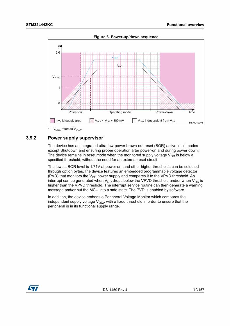
Figure 3. Power-up/down sequence
1. VDDX refers to VDDA.
3.9.2 Power supply supervisor
The device has an integrated ultra-low-power brown-out reset (BOR) active in all modes except Shutdown and ensuring proper operation after power-on and during power down. The device remains in reset mode when the monitored supply voltage VDD is below a specified threshold, without the need for an external reset circuit.
The lowest BOR level is 1.71V at power on, and other higher thresholds can be selected through option bytes.The device features an embedded programmable voltage detector (PVD) that monitors the VDD power supply and compares it to the VPVD threshold. An interrupt can be generated when VDD drops below the VPVD threshold and/or when VDD is higher than the VPVD threshold. The interrupt service routine can then generate a warning message and/or put the MCU into a safe state. The PVD is enabled by software.
In addition, the device embeds a Peripheral Voltage Monitor which compares the independent supply voltage VDDA with a fixed threshold in order to ensure that the peripheral is in its functional supply range.
MSv47490V1
0.3
1
VBOR0
3.6
Operating modePower-on Power-down time
V
VDDX(1)
VDD
Invalid supply area VDDX < VDD + 300 mV VDDX independent from VDD
Functional overview STM32L442KC
20/157 DS11450 Rev 4
3.9.3 Voltage regulator
Two embedded linear voltage regulators supply most of the digital circuitries: the main regulator (MR) and the low-power regulator (LPR).
• The MR is used in the Run and Sleep modes and in the Stop 0 mode.
• The LPR is used in Low-Power Run, Low-Power Sleep, Stop 1 and Stop 2 modes. It is also used to supply the 16 Kbyte SRAM2 in Standby with SRAM2 retention.
• Both regulators are in power-down in Standby and Shutdown modes: the regulator output is in high impedance, and the kernel circuitry is powered down thus inducing zero consumption.
The ultralow-power STM32L442KC supports dynamic voltage scaling to optimize its power consumption in run mode. The voltage from the Main Regulator that supplies the logic (VCORE) can be adjusted according to the system’s maximum operating frequency.
There are two power consumption ranges:
• Range 1 with the CPU running at up to 80 MHz.
• Range 2 with a maximum CPU frequency of 26 MHz. All peripheral clocks are also limited to 26 MHz.
The VCORE can be supplied by the low-power regulator, the main regulator being switched off. The system is then in Low-power run mode.
• Low-power run mode with the CPU running at up to 2 MHz. Peripherals with independent clock can be clocked by HSI16.
3.9.4 Low-power modes
The ultra-low-power STM32L442KC supports seven low-power modes to achieve the best compromise between low-power consumption, short startup time, available peripherals and available wakeup sources.
ST
M3
2L4
42K
CF
un
ction
al ove
rview
DS
11450 R
ev 421/157
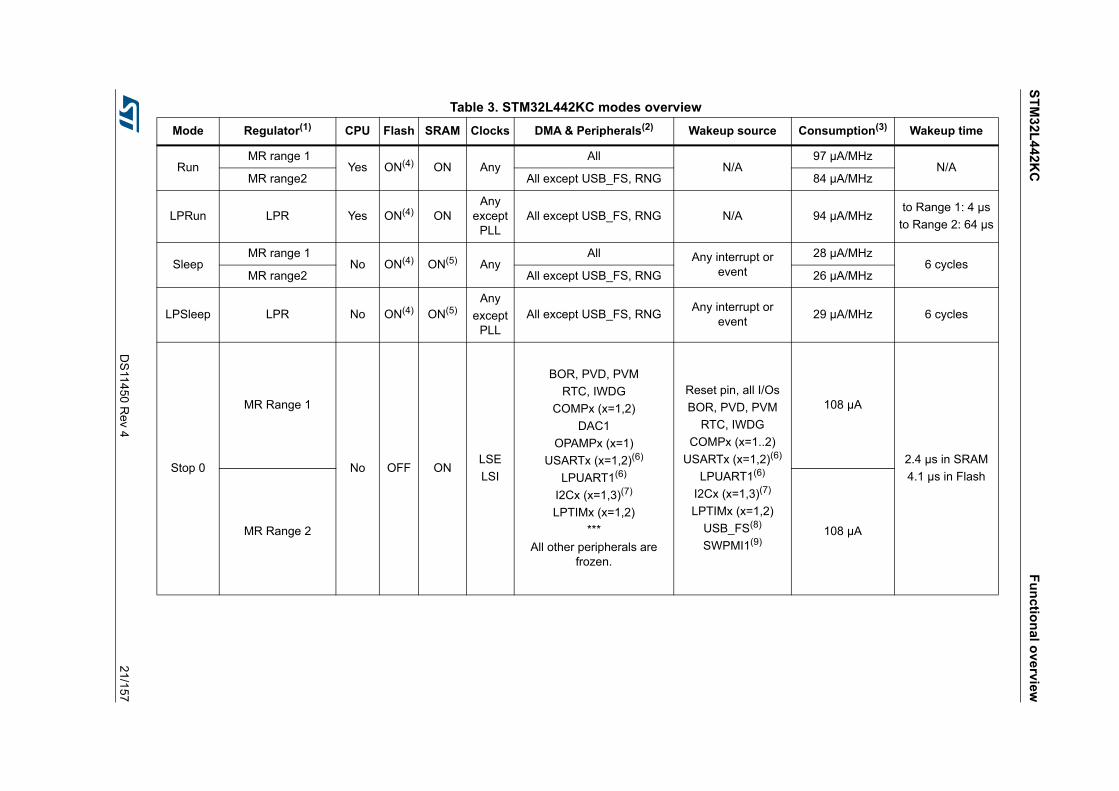
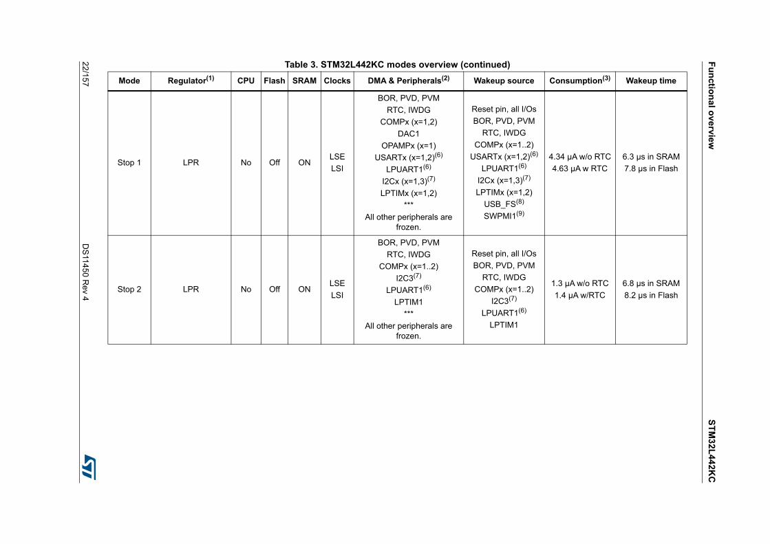
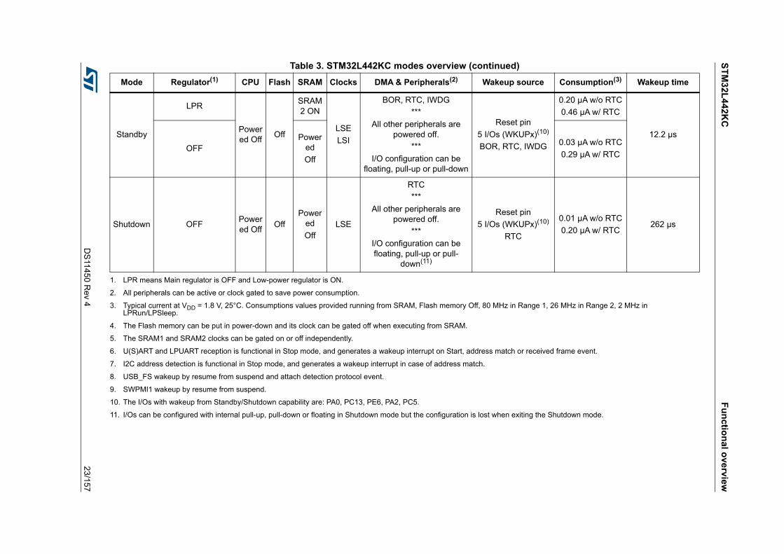
Table 3. STM32L442KC modes overview
Mode Regulator(1) CPU Flash SRAM Clocks DMA & Peripherals(2) Wakeup source Consumption(3) Wakeup time
Run MR range 1
Yes ON(4) ON AnyAll
N/A97 µA/MHz
N/AMR range2 All except USB_FS, RNG 84 µA/MHz
LPRun LPR Yes ON(4) ONAny
except PLL
All except USB_FS, RNG N/A 94 µA/MHzto Range 1: 4 µs
to Range 2: 64 µs
Sleep MR range 1
No ON(4) ON(5) AnyAll Any interrupt or
event
28 µA/MHz6 cycles
MR range2 All except USB_FS, RNG 26 µA/MHz
LPSleep LPR No ON(4) ON(5)Any
except PLL
All except USB_FS, RNGAny interrupt or
event29 µA/MHz 6 cycles
Stop 0
MR Range 1
No OFF ONLSE
LSI
BOR, PVD, PVM
RTC, IWDG
COMPx (x=1,2)
DAC1
OPAMPx (x=1)
USARTx (x=1,2)(6)
LPUART1(6)
I2Cx (x=1,3)(7)
LPTIMx (x=1,2)
***
All other peripherals are frozen.
Reset pin, all I/Os
BOR, PVD, PVM
RTC, IWDG
COMPx (x=1..2)
USARTx (x=1,2)(6)
LPUART1(6)
I2Cx (x=1,3)(7)
LPTIMx (x=1,2)
USB_FS(8)
SWPMI1(9)
108 µA
2.4 µs in SRAM
4.1 µs in Flash
MR Range 2 108 µA
Fu
nctio
nal o
verview
ST
M3
2L
44
2KC
22/1
57D
S114
50 Rev 4
Stop 1 LPR No Off ONLSE
LSI
BOR, PVD, PVM
RTC, IWDG
COMPx (x=1,2)
DAC1
OPAMPx (x=1)
USARTx (x=1,2)(6)
LPUART1(6)
I2Cx (x=1,3)(7)
LPTIMx (x=1,2)
***
All other peripherals are frozen.
Reset pin, all I/Os
BOR, PVD, PVM
RTC, IWDG
COMPx (x=1..2)
USARTx (x=1,2)(6)
LPUART1(6)
I2Cx (x=1,3)(7)
LPTIMx (x=1,2)
USB_FS(8)
SWPMI1(9)
4.34 µA w/o RTC
4.63 µA w RTC
6.3 µs in SRAM
7.8 µs in Flash
Stop 2 LPR No Off ONLSE
LSI
BOR, PVD, PVM
RTC, IWDG
COMPx (x=1..2)
I2C3(7)
LPUART1(6)
LPTIM1
***
All other peripherals are frozen.
Reset pin, all I/Os
BOR, PVD, PVM
RTC, IWDG
COMPx (x=1..2)
I2C3(7)
LPUART1(6)
LPTIM1
1.3 µA w/o RTC
1.4 µA w/RTC
6.8 µs in SRAM
8.2 µs in Flash
Table 3. STM32L442KC modes overview (continued)
Mode Regulator(1) CPU Flash SRAM Clocks DMA & Peripherals(2) Wakeup source Consumption(3) Wakeup time
ST
M3
2L4
42K
CF
un
ction
al ove
rview
DS
11450 R
ev 423/157
Standby
LPR
Powered Off
Off
SRAM2 ON
LSE
LSI
BOR, RTC, IWDG
***
All other peripherals are powered off.
***
I/O configuration can be floating, pull-up or pull-down
Reset pin
5 I/Os (WKUPx)(10)
BOR, RTC, IWDG
0.20 µA w/o RTC
0.46 µA w/ RTC
12.2 µs
OFFPower
ed
Off
0.03 µA w/o RTC
0.29 µA w/ RTC
Shutdown OFFPowered Off
OffPower
ed
OffLSE
RTC
***
All other peripherals are powered off.
***
I/O configuration can be floating, pull-up or pull-
down(11)
Reset pin
5 I/Os (WKUPx)(10)
RTC
0.01 µA w/o RTC
0.20 µA w/ RTC262 µs
1. LPR means Main regulator is OFF and Low-power regulator is ON.
2. All peripherals can be active or clock gated to save power consumption.
3. Typical current at VDD = 1.8 V, 25°C. Consumptions values provided running from SRAM, Flash memory Off, 80 MHz in Range 1, 26 MHz in Range 2, 2 MHz in LPRun/LPSleep.
4. The Flash memory can be put in power-down and its clock can be gated off when executing from SRAM.
5. The SRAM1 and SRAM2 clocks can be gated on or off independently.
6. U(S)ART and LPUART reception is functional in Stop mode, and generates a wakeup interrupt on Start, address match or received frame event.
7. I2C address detection is functional in Stop mode, and generates a wakeup interrupt in case of address match.
8. USB_FS wakeup by resume from suspend and attach detection protocol event.
9. SWPMI1 wakeup by resume from suspend.
10. The I/Os with wakeup from Standby/Shutdown capability are: PA0, PC13, PE6, PA2, PC5.
11. I/Os can be configured with internal pull-up, pull-down or floating in Shutdown mode but the configuration is lost when exiting the Shutdown mode.
Table 3. STM32L442KC modes overview (continued)
Mode Regulator(1) CPU Flash SRAM Clocks DMA & Peripherals(2) Wakeup source Consumption(3) Wakeup time
Functional overview STM32L442KC
24/157 DS11450 Rev 4
By default, the microcontroller is in Run mode after a system or a power Reset. It is up to the user to select one of the low-power modes described below:
• Sleep mode
In Sleep mode, only the CPU is stopped. All peripherals continue to operate and can wake up the CPU when an interrupt/event occurs.
• Low-power run mode
This mode is achieved with VCORE supplied by the low-power regulator to minimize the regulator's operating current. The code can be executed from SRAM or from Flash, and the CPU frequency is limited to 2 MHz. The peripherals with independent clock can be clocked by HSI16.
• Low-power sleep mode
This mode is entered from the low-power run mode. Only the CPU clock is stopped. When wakeup is triggered by an event or an interrupt, the system reverts to the low-power run mode.
• Stop 0, Stop 1 and Stop 2 modes
Stop mode achieves the lowest power consumption while retaining the content of SRAM and registers. All clocks in the VCORE domain are stopped, the PLL, the MSI RC and the HSI16 RC are disabled. The LSE or LSI is still running.
The RTC can remain active (Stop mode with RTC, Stop mode without RTC).
Some peripherals with wakeup capability can enable the HSI16 RC during Stop mode to detect their wakeup condition.
Three Stop modes are available: Stop 0, Stop 1 and Stop 2 modes. In Stop 2 mode, most of the VCORE domain is put in a lower leakage mode.
Stop 1 offers the largest number of active peripherals and wakeup sources, a smaller wakeup time but a higher consumption than Stop 2. In Stop 0 mode, the main regulator remains ON, allowing a very fast wakeup time but with much higher consumption.
The system clock when exiting from Stop 0, Stop 1 or Stop 2 modes can be either MSI up to 48 MHz or HSI16, depending on software configuration.
• Standby mode
The Standby mode is used to achieve the lowest power consumption with BOR. The internal regulator is switched off so that the VCORE domain is powered off. The PLL, the MSI RC and the HSI16 RC are also switched off.
The RTC can remain active (Standby mode with RTC, Standby mode without RTC).
The brown-out reset (BOR) always remains active in Standby mode.
The state of each I/O during standby mode can be selected by software: I/O with internal pull-up, internal pull-down or floating.
After entering Standby mode, SRAM1 and register contents are lost except for registers in the Backup domain and Standby circuitry. Optionally, SRAM2 can be retained in Standby mode, supplied by the low-power Regulator (Standby with SRAM2 retention mode).
The device exits Standby mode when an external reset (NRST pin), an IWDG reset, WKUP pin event (configurable rising or falling edge), or an RTC event occurs (alarm, periodic wakeup, timestamp, tamper) or a failure is detected on LSE (CSS on LSE).
The system clock after wakeup is MSI up to 8 MHz.
DS11450 Rev 4 25/157
STM32L442KC Functional overview
51
• Shutdown mode
The Shutdown mode allows to achieve the lowest power consumption. The internal regulator is switched off so that the VCORE domain is powered off. The PLL, the HSI16, the MSI and the LSI oscillators are also switched off.
The RTC can remain active (Shutdown mode with RTC, Shutdown mode without RTC).
The BOR is not available in Shutdown mode. No power voltage monitoring is possible in this mode, therefore the switch to Backup domain is not supported.
SRAM1, SRAM2 and register contents are lost except for registers in the Backup domain.
The device exits Shutdown mode when an external reset (NRST pin), a WKUP pin event (configurable rising or falling edge), or an RTC event occurs (alarm, periodic wakeup, timestamp, tamper).
The system clock after wakeup is MSI at 4 MHz.
Functional overview STM32L442KC
26/157 DS11450 Rev 4
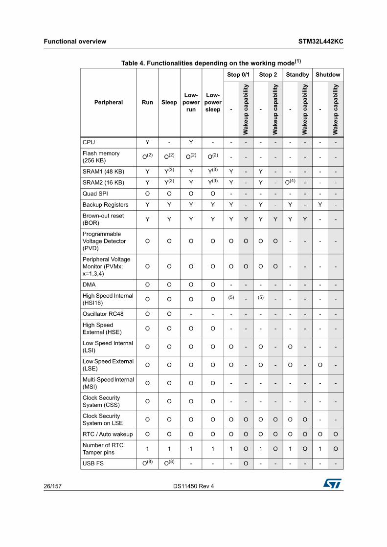
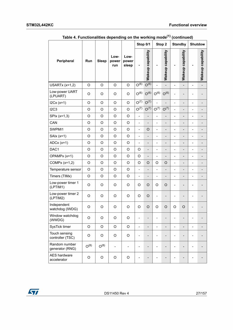
Table 4. Functionalities depending on the working mode(1)
Peripheral Run SleepLow-
power run
Low-power sleep
Stop 0/1 Stop 2 Standby Shutdow
-
Wak
eup
cap
abili
ty
-
Wak
eup
cap
abili
ty
-
Wak
eup
cap
abili
ty
-
Wak
eup
cap
abili
ty
CPU Y - Y - - - - - - - - -
Flash memory (256 KB)
O(2) O(2) O(2) O(2) - - - - - - - -
SRAM1 (48 KB) Y Y(3) Y Y(3) Y - Y - - - - -
SRAM2 (16 KB) Y Y(3) Y Y(3) Y - Y - O(4) - - -
Quad SPI O O O O - - - - - - - -
Backup Registers Y Y Y Y Y - Y - Y - Y -
Brown-out reset (BOR)
Y Y Y Y Y Y Y Y Y Y - -
Programmable Voltage Detector (PVD)
O O O O O O O O - - - -
Peripheral Voltage Monitor (PVMx; x=1,3,4)
O O O O O O O O - - - -
DMA O O O O - - - - - - - -
High Speed Internal (HSI16)
O O O O (5) - (5) - - - - -
Oscillator RC48 O O - - - - - - - - - -
High Speed External (HSE)
O O O O - - - - - - - -
Low Speed Internal (LSI)
O O O O O - O - O - - -
Low Speed External (LSE)
O O O O O - O - O - O -
Multi-Speed Internal (MSI)
O O O O - - - - - - - -
Clock Security System (CSS)
O O O O - - - - - - - -
Clock Security System on LSE
O O O O O O O O O O - -
RTC / Auto wakeup O O O O O O O O O O O O
Number of RTC Tamper pins
1 1 1 1 1 O 1 O 1 O 1 O
USB FS O(8) O(8) - - - O - - - - - -
DS11450 Rev 4 27/157
STM32L442KC Functional overview
51
USARTx (x=1,2) O O O O O(6) O(6) - - - - - -
Low-power UART (LPUART)
O O O O O(6) O(6) O(6) O(6) - - - -
I2Cx (x=1) O O O O O(7) O(7) - - - - - -
I2C3 O O O O O(7) O(7) O(7) O(7) - - - -
SPIx (x=1,3) O O O O - - - - - - - -
CAN O O O O - - - - - - - -
SWPMI1 O O O O - O - - - - - -
SAIx (x=1) O O O O - - - - - - - -
ADCx (x=1) O O O O - - - - - - - -
DAC1 O O O O O - - - - - - -
OPAMPx (x=1) O O O O O - - - - - - -
COMPx (x=1,2) O O O O O O O O - - - -
Temperature sensor O O O O - - - - - - - -
Timers (TIMx) O O O O - - - - - - - -
Low-power timer 1 (LPTIM1)
O O O O O O O O - - - -
Low-power timer 2 (LPTIM2)
O O O O O O - - - - - -
Independent watchdog (IWDG)
O O O O O O O O O O - -
Window watchdog (WWDG)
O O O O - - - - - - - -
SysTick timer O O O O - - - - - - - -
Touch sensing controller (TSC)
O O O O - - - - - - - -
Random number generator (RNG)
O(8) O(8) - - - - - - - - - -
AES hardware accelerator
O O O O - - - - - - - -
Table 4. Functionalities depending on the working mode(1) (continued)
Peripheral Run SleepLow-
power run
Low-power sleep
Stop 0/1 Stop 2 Standby Shutdow
-
Wa
keu
p c
ap
abili
ty
-
Wa
keu
p c
ap
abili
ty
-
Wa
keu
p c
ap
abili
ty
-
Wa
keu
p c
ap
abili
ty
Functional overview STM32L442KC
28/157 DS11450 Rev 4
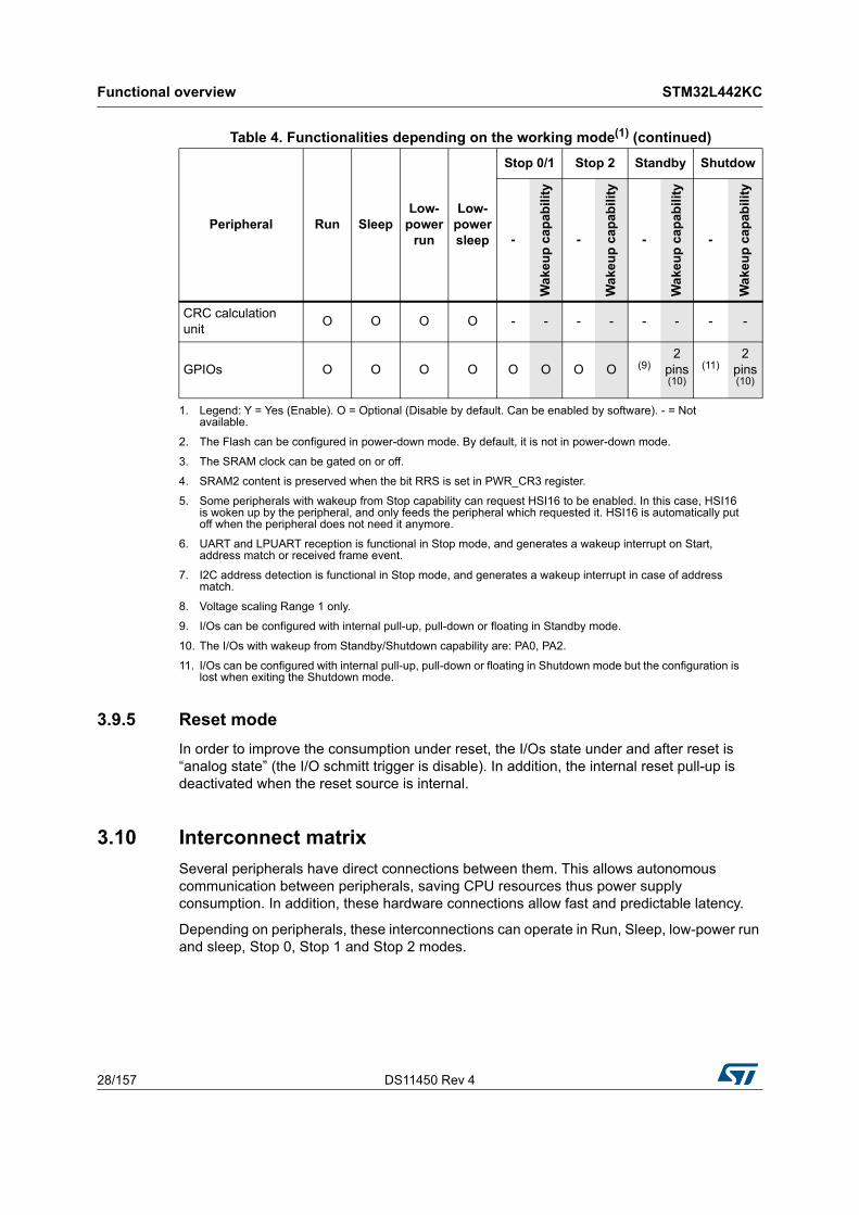
3.9.5 Reset mode
In order to improve the consumption under reset, the I/Os state under and after reset is “analog state” (the I/O schmitt trigger is disable). In addition, the internal reset pull-up is deactivated when the reset source is internal.
3.10 Interconnect matrix
Several peripherals have direct connections between them. This allows autonomous communication between peripherals, saving CPU resources thus power supply consumption. In addition, these hardware connections allow fast and predictable latency.
Depending on peripherals, these interconnections can operate in Run, Sleep, low-power run and sleep, Stop 0, Stop 1 and Stop 2 modes.
CRC calculation unit
O O O O - - - - - - - -
GPIOs O O O O O O O O (9)2
pins(10)
(11)2
pins(10)
1. Legend: Y = Yes (Enable). O = Optional (Disable by default. Can be enabled by software). - = Not available.
2. The Flash can be configured in power-down mode. By default, it is not in power-down mode.
3. The SRAM clock can be gated on or off.
4. SRAM2 content is preserved when the bit RRS is set in PWR_CR3 register.
5. Some peripherals with wakeup from Stop capability can request HSI16 to be enabled. In this case, HSI16 is woken up by the peripheral, and only feeds the peripheral which requested it. HSI16 is automatically put off when the peripheral does not need it anymore.
6. UART and LPUART reception is functional in Stop mode, and generates a wakeup interrupt on Start, address match or received frame event.
7. I2C address detection is functional in Stop mode, and generates a wakeup interrupt in case of address match.
8. Voltage scaling Range 1 only.
9. I/Os can be configured with internal pull-up, pull-down or floating in Standby mode.
10. The I/Os with wakeup from Standby/Shutdown capability are: PA0, PA2.
11. I/Os can be configured with internal pull-up, pull-down or floating in Shutdown mode but the configuration is lost when exiting the Shutdown mode.
Table 4. Functionalities depending on the working mode(1) (continued)
Peripheral Run SleepLow-
power run
Low-power sleep
Stop 0/1 Stop 2 Standby Shutdow
-
Wa
keu
p c
ap
abili
ty
-
Wa
keu
p c
ap
abili
ty
-
Wa
keu
p c
ap
abili
ty
-
Wa
keu
p c
ap
abili
ty
DS11450 Rev 4 29/157
STM32L442KC Functional overview
51
Table 5. STM32L442KC peripherals interconnect matrix
Interconnect sourceInterconnect destination
Interconnect action
Ru
n
Sle
ep
Lo
w-p
ow
er r
un
Lo
w-p
ow
er s
leep
Sto
p 0
/ S
top
1
Sto
p 2
TIMx
TIMx Timers synchronization or chaining Y Y Y Y - -
ADCx
DAC1Conversion triggers Y Y Y Y - -
DMA Memory to memory transfer trigger Y Y Y Y - -
COMPx Comparator output blanking Y Y Y Y - -
TIM15/TIM16 IRTIM Infrared interface output generation Y Y Y Y - -
COMPx
TIM1
TIM2Timer input channel, trigger, break from analog signals comparison
Y Y Y Y - -
LPTIMERxLow-power timer triggered by analog signals comparison
Y Y Y Y YY(1)
ADCx TIM1 Timer triggered by analog watchdog Y Y Y Y - -
RTC
TIM16 Timer input channel from RTC events Y Y Y Y - -
LPTIMERxLow-power timer triggered by RTC alarms or tampers
Y Y Y Y YY(1)
All clocks sources (internal and external)
TIM2
TIM15, 16Clock source used as input channel for RC measurement and trimming
Y Y Y Y - -
USB TIM2 Timer triggered by USB SOF Y Y - - - -
CSS
CPU (hard fault)
RAM (parity error)
Flash memory (ECC error)
COMPx
PVD
TIM1
TIM15,16Timer break Y Y Y Y - -
GPIO
TIMx External trigger Y Y Y Y - -
LPTIMERx External trigger Y Y Y Y YY(1)
ADCx
DAC1Conversion external trigger Y Y Y Y - -
1. LPTIM1 only.
Functional overview STM32L442KC
30/157 DS11450 Rev 4
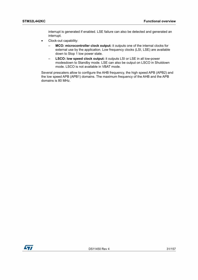
3.11 Clocks and startup
The clock controller (see Figure 4) distributes the clocks coming from different oscillators to the core and the peripherals. It also manages clock gating for low-power modes and ensures clock robustness. It features:
• Clock prescaler: to get the best trade-off between speed and current consumption, the clock frequency to the CPU and peripherals can be adjusted by a programmable prescaler
• Safe clock switching: clock sources can be changed safely on the fly in run mode through a configuration register.
• Clock management: to reduce power consumption, the clock controller can stop the clock to the core, individual peripherals or memory.
• System clock source: four different clock sources can be used to drive the master clock SYSCLK:
– High Speed External clock (HSE) can supply a PLL.
– 16 MHz high-speed internal RC oscillator (HSI16), trimmable by software, that can supply a PLL
– Multispeed internal RC oscillator (MSI), trimmable by software, able to generate 12 frequencies from 100 kHz to 48 MHz. When a 32.768 kHz clock source is available in the system (LSE), the MSI frequency can be automatically trimmed by hardware to reach better than ±0.25% accuracy. In this mode the MSI can feed the USB device. The MSI can supply a PLL.
– System PLL which can be fed by HSE, HSI16 or MSI, with a maximum frequency at 80 MHz.
• RC48 with clock recovery system (HSI48): internal RC48 MHz clock source can be used to drive the USB or the RNG peripherals. This clock can be output on the MCO.
• Auxiliary clock source: two ultralow-power clock sources that can be used to drive the real-time clock:
– 32.768 kHz low-speed external crystal (LSE), supporting four drive capability modes. The LSE can also be configured in bypass mode for an external clock.
– 32 kHz low-speed internal RC (LSI), also used to drive the independent watchdog. The LSI clock accuracy is ±5% accuracy.
• Peripheral clock sources: Several peripherals (USB, RNG, SAI, USARTs, I2Cs, LPTimers, ADC, SWPMI) have their own independent clock whatever the system clock. Two PLLs, each having three independent outputs allowing the highest flexibility, can generate independent clocks for the ADC, the USB/RNG and the SAI.
• Startup clock: after reset, the microcontroller restarts by default with an internal 4 MHz clock (MSI). The prescaler ratio and clock source can be changed by the application program as soon as the code execution starts.
• Clock security system (CSS): this feature can be enabled by software. If a HSE clock failure occurs, the master clock is automatically switched to HSI16 and a software
DS11450 Rev 4 31/157
STM32L442KC Functional overview
51
interrupt is generated if enabled. LSE failure can also be detected and generated an interrupt.
• Clock-out capability:
– MCO: microcontroller clock output: it outputs one of the internal clocks for external use by the application. Low frequency clocks (LSI, LSE) are available down to Stop 1 low power state.
– LSCO: low speed clock output: it outputs LSI or LSE in all low-power modesdown to Standby mode. LSE can also be output on LSCO in Shutdown mode. LSCO is not available in VBAT mode.
Several prescalers allow to configure the AHB frequency, the high speed APB (APB2) and the low speed APB (APB1) domains. The maximum frequency of the AHB and the APB domains is 80 MHz.
Functional overview STM32L442KC
32/157 DS11450 Rev 4
Figure 4. Clock tree
MSv39217V4
SYSCLK
MCO
LSCO
48 MHz clock to USB, RNG
to IWDG
to RTC
to PWR
HCLK
to AHB bus, core, memory and DMA
FCLK Cortex free running clock
to Cortex system timer
to APB1 peripherals
to APB2 peripherals
PCLK1
PCLK2
LSEHSI16
SYSCLKto USARTx
x=2..3to LPUART1
to I2Cxx=1,2,3
to LPTIMxx=1,2
SAI1_EXTCLK
to SWPMI
to TIMxx=2,6,7
OSC32_OUT
OSC32_IN
MSIHSI16
HSE
HSI16
LSI
LSE
HSE
SYSCLK
HSE
MSI
HSI16
LSE OSC32.768 kHz /32
AHB PRESC/ 1,2,..512
/ 8
APB1 PRESC/ 1,2,4,8,16
x1 or x2
HSI16SYSCLK
LSILSE
HSI16
HSI16
APB2 PRESC/ 1,2,4,8,16
to TIMxx=1,15,16
x1 or x2
to USART1LSE
HSI16SYSCLK
/ M
MSI RC100 kHz – 48 MHz
HSI RC16 MHz
Clock detectorCK_IN
/ 1
LSI RC 32 kHz
Clock source control
PLLSAI1CLK
PLL48M1CLK
PLLCLK
PLLSAI2CLK
PLL48M2CLK
PLLADC1CLK
HSI48
PLL
PLLSAI1
VCO FVCO / P
/ R
/ Q
/ P
/ Q
/ R
VCO FVCO
MSI
PLLCLK
to ADC
to SAI1
MSI
SYSCLK
HSI16
HSI RC48 MHz
CRS
HSI16
DS11450 Rev 4 33/157
STM32L442KC Functional overview
51
3.12 General-purpose inputs/outputs (GPIOs)
Each of the GPIO pins can be configured by software as output (push-pull or open-drain), as input (with or without pull-up or pull-down) or as peripheral alternate function. Most of the GPIO pins are shared with digital or analog alternate functions. Fast I/O toggling can be achieved thanks to their mapping on the AHB2 bus.
The I/Os alternate function configuration can be locked if needed following a specific sequence in order to avoid spurious writing to the I/Os registers.
3.13 Direct memory access controller (DMA)
The device embeds 2 DMAs. Refer to Table 6: DMA implementation for the features implementation.
Direct memory access (DMA) is used in order to provide high-speed data transfer between peripherals and memory as well as memory to memory. Data can be quickly moved by DMA without any CPU actions. This keeps CPU resources free for other operations.
The two DMA controllers have 14 channels in total, each dedicated to managing memory access requests from one or more peripherals. Each has an arbiter for handling the priority between DMA requests.
The DMA supports:
• 14 independently configurable channels (requests)
• Each channel is connected to dedicated hardware DMA requests, software trigger is also supported on each channel. This configuration is done by software.
• Priorities between requests from channels of one DMA are software programmable (4 levels consisting of very high, high, medium, low) or hardware in case of equality (request 1 has priority over request 2, etc.)
• Independent source and destination transfer size (byte, half word, word), emulating packing and unpacking. Source/destination addresses must be aligned on the data size.
• Support for circular buffer management
• 3 event flags (DMA Half Transfer, DMA Transfer complete and DMA Transfer Error) logically ORed together in a single interrupt request for each channel
• Memory-to-memory transfer
• Peripheral-to-memory and memory-to-peripheral, and peripheral-to-peripheral transfers
• Access to Flash, SRAM, APB and AHB peripherals as source and destination
• Programmable number of data to be transferred: up to 65536.
Table 6. DMA implementation
DMA features DMA1 DMA2
Number of regular channels 7 7
Functional overview STM32L442KC
34/157 DS11450 Rev 4
3.14 Interrupts and events
3.14.1 Nested vectored interrupt controller (NVIC)
The devices embed a nested vectored interrupt controller able to manage 16 priority levels, and handle up to 61 maskable interrupt channels plus the 16 interrupt lines of the Cortex®-M4.
The NVIC benefits are the following:
• Closely coupled NVIC gives low latency interrupt processing
• Interrupt entry vector table address passed directly to the core
• Allows early processing of interrupts
• Processing of late arriving higher priority interrupts
• Support for tail chaining
• Processor state automatically saved on interrupt entry, and restored on interrupt exit, with no instruction overhead
The NVIC hardware block provides flexible interrupt management features with minimal interrupt latency.
3.14.2 Extended interrupt/event controller (EXTI)
The extended interrupt/event controller consists of 34 edge detector lines used to generate interrupt/event requests and wake-up the system from Stop mode. Each external line can be independently configured to select the trigger event (rising edge, falling edge, both) and can be masked independently. A pending register maintains the status of the interrupt requests. The internal lines are connected to peripherals with wakeup from Stop mode capability. The EXTI can detect an external line with a pulse width shorter than the internal clock period. Up to 26 GPIOs can be connected to the 16 external interrupt lines.
DS11450 Rev 4 35/157
STM32L442KC Functional overview
51
3.15 Analog to digital converter (ADC)
The device embeds a successive approximation analog-to-digital converter with the following features:
• 12-bit native resolution, with built-in calibration
• 5.33 Msps maximum conversion rate with full resolution
– Down to 18.75 ns sampling time
– Increased conversion rate for lower resolution (up to 8.88 Msps for 6-bit resolution)
• Up to 10 external channels.
• 4 internal channels: internal reference voltage, temperature sensor, DAC1_OUT1 and DAC1_OUT2.
• Single-ended and differential mode inputs
• Low-power design
– Capable of low-current operation at low conversion rate (consumption decreases linearly with speed)
– Dual clock domain architecture: ADC speed independent from CPU frequency
• Highly versatile digital interface
– Single-shot or continuous/discontinuous sequencer-based scan mode: 2 groups of analog signals conversions can be programmed to differentiate background and high-priority real-time conversions
– ADC supports multiple trigger inputs for synchronization with on-chip timers and external signals
– Results stored into data register or in RAM with DMA controller support
– Data pre-processing: left/right alignment and per channel offset compensation
– Built-in oversampling unit for enhanced SNR
– Channel-wise programmable sampling time
– Three analog watchdog for automatic voltage monitoring, generating interrupts and trigger for selected timers
– Hardware assistant to prepare the context of the injected channels to allow fast context switching
3.15.1 Temperature sensor
The temperature sensor (TS) generates a voltage VTS that varies linearly with temperature.
The temperature sensor is internally connected to the ADC1_IN17 input channel which is used to convert the sensor output voltage into a digital value.
The sensor provides good linearity but it has to be calibrated to obtain good overall accuracy of the temperature measurement. As the offset of the temperature sensor varies from chip to chip due to process variation, the uncalibrated internal temperature sensor is suitable for applications that detect temperature changes only.
To improve the accuracy of the temperature sensor measurement, each device is individually factory-calibrated by ST. The temperature sensor factory calibration data are stored by ST in the system memory area, accessible in read-only mode.
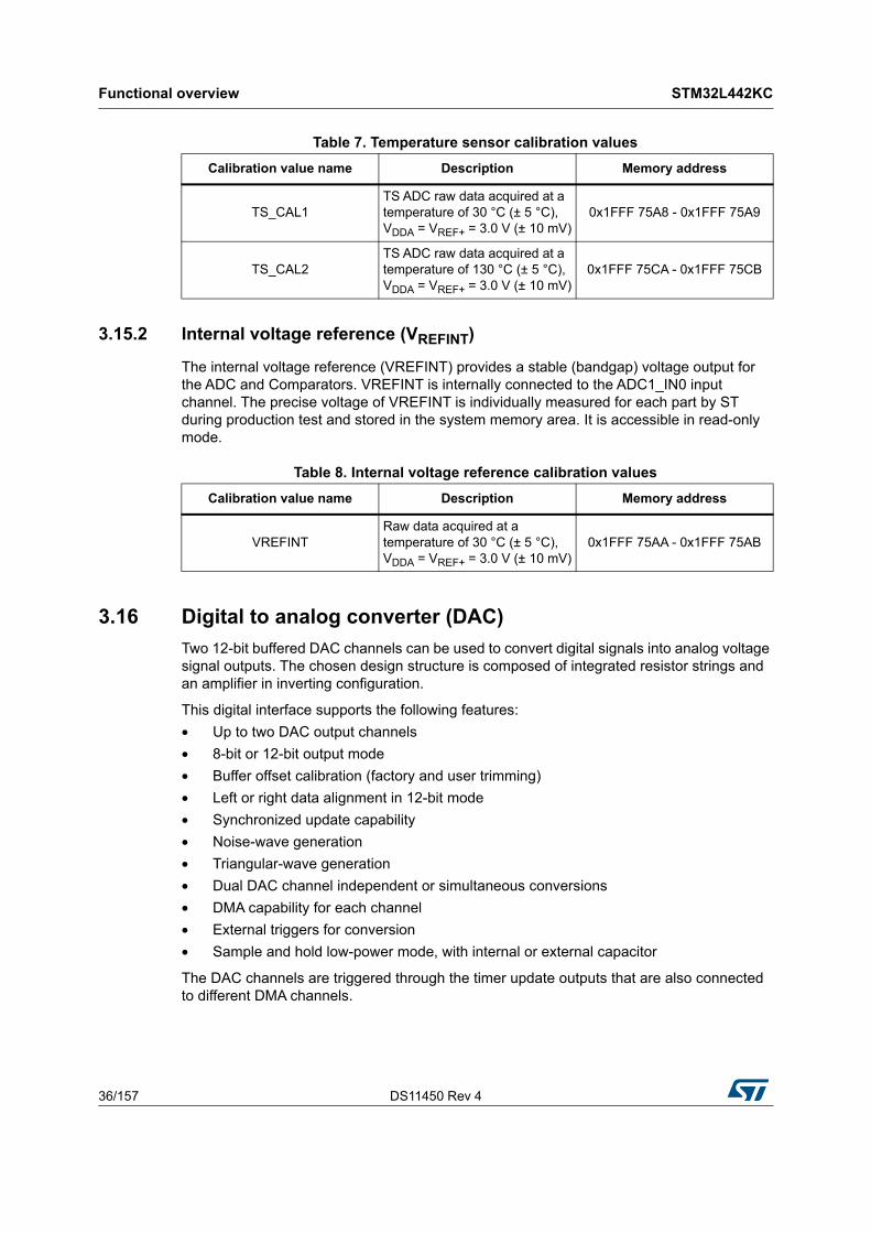
Functional overview STM32L442KC
36/157 DS11450 Rev 4
3.15.2 Internal voltage reference (VREFINT)
The internal voltage reference (VREFINT) provides a stable (bandgap) voltage output for the ADC and Comparators. VREFINT is internally connected to the ADC1_IN0 input channel. The precise voltage of VREFINT is individually measured for each part by ST during production test and stored in the system memory area. It is accessible in read-only mode.
3.16 Digital to analog converter (DAC)
Two 12-bit buffered DAC channels can be used to convert digital signals into analog voltage signal outputs. The chosen design structure is composed of integrated resistor strings and an amplifier in inverting configuration.
This digital interface supports the following features:
• Up to two DAC output channels
• 8-bit or 12-bit output mode
• Buffer offset calibration (factory and user trimming)
• Left or right data alignment in 12-bit mode
• Synchronized update capability
• Noise-wave generation
• Triangular-wave generation
• Dual DAC channel independent or simultaneous conversions
• DMA capability for each channel
• External triggers for conversion
• Sample and hold low-power mode, with internal or external capacitor
The DAC channels are triggered through the timer update outputs that are also connected to different DMA channels.
Table 7. Temperature sensor calibration values
Calibration value name Description Memory address
TS_CAL1TS ADC raw data acquired at a temperature of 30 °C (± 5 °C), VDDA = VREF+ = 3.0 V (± 10 mV)
0x1FFF 75A8 - 0x1FFF 75A9
TS_CAL2TS ADC raw data acquired at a temperature of 130 °C (± 5 °C), VDDA = VREF+ = 3.0 V (± 10 mV)
0x1FFF 75CA - 0x1FFF 75CB
Table 8. Internal voltage reference calibration values
Calibration value name Description Memory address
VREFINTRaw data acquired at a temperature of 30 °C (± 5 °C), VDDA = VREF+ = 3.0 V (± 10 mV)
0x1FFF 75AA - 0x1FFF 75AB
DS11450 Rev 4 37/157
STM32L442KC Functional overview
51
3.17 Comparators (COMP)
The STM32L442KC devices embed two rail-to-rail comparators with programmable reference voltage (internal or external), hysteresis and speed (low speed for low-power) and with selectable output polarity.
The reference voltage can be one of the following:
• External I/O
• DAC output channels
• Internal reference voltage or submultiple (1/4, 1/2, 3/4).
All comparators can wake up from Stop mode, generate interrupts and breaks for the timers and can be also combined into a window comparator.
3.18 Operational amplifier (OPAMP)
The STM32L442KC embeds one operational amplifier with external or internal follower routing and PGA capability.
The operational amplifier features:
• Low input bias current
• Low offset voltage
• Low-power mode
• Rail-to-rail input
3.19 Touch sensing controller (TSC)
The touch sensing controller provides a simple solution for adding capacitive sensing functionality to any application. Capacitive sensing technology is able to detect finger presence near an electrode which is protected from direct touch by a dielectric (glass, plastic, ...). The capacitive variation introduced by the finger (or any conductive object) is measured using a proven implementation based on a surface charge transfer acquisition principle.
The touch sensing controller is fully supported by the STMTouch touch sensing firmware library which is free to use and allows touch sensing functionality to be implemented reliably in the end application.

Functional overview STM32L442KC
38/157 DS11450 Rev 4
The main features of the touch sensing controller are the following:
• Proven and robust surface charge transfer acquisition principle
• Supports up to 3 capacitive sensing channels
• Up to 3 capacitive sensing channels can be acquired in parallel offering a very good response time
• Spread spectrum feature to improve system robustness in noisy environments
• Full hardware management of the charge transfer acquisition sequence
• Programmable charge transfer frequency
• Programmable sampling capacitor I/O pin
• Programmable channel I/O pin
• Programmable max count value to avoid long acquisition when a channel is faulty
• Dedicated end of acquisition and max count error flags with interrupt capability
• One sampling capacitor for up to 3 capacitive sensing channels to reduce the system components
• Compatible with proximity, touchkey, linear and rotary touch sensor implementation
• Designed to operate with STMTouch touch sensing firmware library
Note: The number of capacitive sensing channels is dependent on the size of the packages and subject to I/O availability.
3.20 Random number generator (RNG)
All devices embed an RNG that delivers 32-bit random numbers generated by an integrated analog circuit.
3.21 Advanced encryption standard hardware accelerator (AES)
The devices embed an AES hardware accelerator can be used to both encipher and
decipher data using AES algorithm.
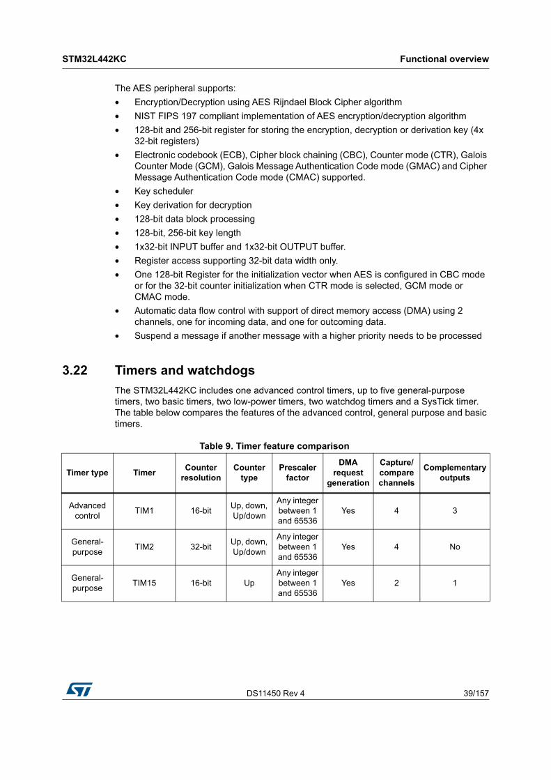
DS11450 Rev 4 39/157
STM32L442KC Functional overview
51
The AES peripheral supports:
• Encryption/Decryption using AES Rijndael Block Cipher algorithm
• NIST FIPS 197 compliant implementation of AES encryption/decryption algorithm
• 128-bit and 256-bit register for storing the encryption, decryption or derivation key (4x 32-bit registers)
• Electronic codebook (ECB), Cipher block chaining (CBC), Counter mode (CTR), Galois Counter Mode (GCM), Galois Message Authentication Code mode (GMAC) and Cipher Message Authentication Code mode (CMAC) supported.
• Key scheduler
• Key derivation for decryption
• 128-bit data block processing
• 128-bit, 256-bit key length
• 1x32-bit INPUT buffer and 1x32-bit OUTPUT buffer.
• Register access supporting 32-bit data width only.
• One 128-bit Register for the initialization vector when AES is configured in CBC mode or for the 32-bit counter initialization when CTR mode is selected, GCM mode or CMAC mode.
• Automatic data flow control with support of direct memory access (DMA) using 2 channels, one for incoming data, and one for outcoming data.
• Suspend a message if another message with a higher priority needs to be processed
3.22 Timers and watchdogs
The STM32L442KC includes one advanced control timers, up to five general-purpose timers, two basic timers, two low-power timers, two watchdog timers and a SysTick timer. The table below compares the features of the advanced control, general purpose and basic timers.
Table 9. Timer feature comparison
Timer type TimerCounter
resolutionCounter
typePrescaler
factor
DMA request
generation
Capture/compare channels
Complementary outputs
Advanced control
TIM1 16-bitUp, down, Up/down
Any integer between 1 and 65536
Yes 4 3
General-purpose
TIM2 32-bitUp, down, Up/down
Any integer between 1 and 65536
Yes 4 No
General-purpose
TIM15 16-bit UpAny integer between 1 and 65536
Yes 2 1
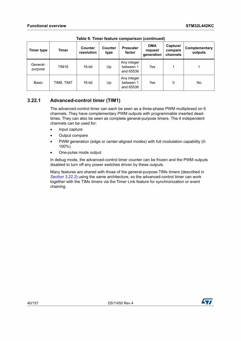
Functional overview STM32L442KC
40/157 DS11450 Rev 4
3.22.1 Advanced-control timer (TIM1)
The advanced-control timer can each be seen as a three-phase PWM multiplexed on 6 channels. They have complementary PWM outputs with programmable inserted dead-times. They can also be seen as complete general-purpose timers. The 4 independent channels can be used for:
• Input capture
• Output compare
• PWM generation (edge or center-aligned modes) with full modulation capability (0-100%)
• One-pulse mode output
In debug mode, the advanced-control timer counter can be frozen and the PWM outputs disabled to turn off any power switches driven by these outputs.
Many features are shared with those of the general-purpose TIMx timers (described in Section 3.22.2) using the same architecture, so the advanced-control timer can work together with the TIMx timers via the Timer Link feature for synchronization or event chaining.
General-purpose
TIM16 16-bit UpAny integer between 1 and 65536
Yes 1 1
Basic TIM6, TIM7 16-bit UpAny integer between 1 and 65536
Yes 0 No
Table 9. Timer feature comparison (continued)
Timer type TimerCounter
resolutionCounter
typePrescaler
factor
DMA request
generation
Capture/compare channels
Complementary outputs
DS11450 Rev 4 41/157
STM32L442KC Functional overview
51
3.22.2 General-purpose timers (TIM2, TIM15, TIM16)
There are up to three synchronizable general-purpose timers embedded in the STM32L442KC (see Table 9 for differences). Each general-purpose timer can be used to generate PWM outputs, or act as a simple time base.
• TIM2
It is a full-featured general-purpose timer:
TIM2 has a 32-bit auto-reload up/downcounter and 32-bit prescaler.
This timer features 4 independent channels for input capture/output compare, PWM or one-pulse mode output. It can work with the other general-purpose timers via the Timer Link feature for synchronization or event chaining.
The counter can be frozen in debug mode.
It has independent DMA request generation and support quadrature encoder.
• TIM15 and 16
They are general-purpose timers with mid-range features:
They have 16-bit auto-reload upcounters and 16-bit prescalers.
– TIM15 has 2 channels and 1 complementary channel
– TIM16 has 1 channel and 1 complementary channel
All channels can be used for input capture/output compare, PWM or one-pulse mode output.
The timers can work together via the Timer Link feature for synchronization or event chaining. The timers have independent DMA request generation.
The counters can be frozen in debug mode.
3.22.3 Basic timers (TIM6 and TIM7)
The basic timers are mainly used for DAC trigger generation. They can also be used as generic 16-bit timebases.
3.22.4 Low-power timer (LPTIM1 and LPTIM2)
The devices embed two low-power timers. These timers have an independent clock and are running in Stop mode if they are clocked by LSE, LSI or an external clock. They are able to wakeup the system from Stop mode.
LPTIM1 is active in Stop 0, Stop 1 and Stop 2 modes.
LPTIM2 is active in Stop 0 and Stop 1 mode.
Functional overview STM32L442KC
42/157 DS11450 Rev 4
This low-power timer supports the following features:
• 16-bit up counter with 16-bit autoreload register
• 16-bit compare register
• Configurable output: pulse, PWM
• Continuous/ one shot mode
• Selectable software/hardware input trigger
• Selectable clock source
– Internal clock sources: LSE, LSI, HSI16 or APB clock
– External clock source over LPTIM input (working even with no internal clock source running, used by pulse counter application).
• Programmable digital glitch filter
• Encoder mode (LPTIM1 only)
3.22.5 Infrared interface (IRTIM)
The STM32L442KC includes one infrared interface (IRTIM). It can be used with an infrared LED to perform remote control functions. It uses TIM15 and TIM16 output channels to generate output signal waveforms on IR_OUT pin.
3.22.6 Independent watchdog (IWDG)
The independent watchdog is based on a 12-bit downcounter and 8-bit prescaler. It is clocked from an independent 32 kHz internal RC (LSI) and as it operates independently from the main clock, it can operate in Stop and Standby modes. It can be used either as a watchdog to reset the device when a problem occurs, or as a free running timer for application timeout management. It is hardware or software configurable through the option bytes. The counter can be frozen in debug mode.
3.22.7 System window watchdog (WWDG)
The window watchdog is based on a 7-bit downcounter that can be set as free running. It can be used as a watchdog to reset the device when a problem occurs. It is clocked from the main clock. It has an early warning interrupt capability and the counter can be frozen in debug mode.
3.22.8 SysTick timer
This timer is dedicated to real-time operating systems, but could also be used as a standard down counter. It features:
• A 24-bit down counter
• Autoreload capability
• Maskable system interrupt generation when the counter reaches 0.
• Programmable clock source
DS11450 Rev 4 43/157
STM32L442KC Functional overview
51
3.23 Real-time clock (RTC) and backup registers
The RTC is an independent BCD timer/counter. It supports the following features:
• Calendar with subsecond, seconds, minutes, hours (12 or 24 format), week day, date, month, year, in BCD (binary-coded decimal) format.
• Automatic correction for 28, 29 (leap year), 30, and 31 days of the month.
• Two programmable alarms.
• On-the-fly correction from 1 to 32767 RTC clock pulses. This can be used to synchronize it with a master clock.
• Reference clock detection: a more precise second source clock (50 or 60 Hz) can be used to enhance the calendar precision.
• Digital calibration circuit with 0.95 ppm resolution, to compensate for quartz crystal inaccuracy.
• One anti-tamper detection pin with programmable filter.
• Timestamp feature which can be used to save the calendar content. This function can be triggered by an event on the timestamp pin, or by a tamper event.
• 17-bit auto-reload wakeup timer (WUT) for periodic events with programmable resolution and period.
The RTC and the 32 backup registers are supplied through a switch that takes power from the VDD supply.
The backup registers are 32-bit registers used to store 128 bytes of user application data when VDD power is not present. They are not reset by a system or power reset, or when the device wakes up from Standby or Shutdown mode.
The RTC clock sources can be:
• A 32.768 kHz external crystal (LSE)
• An external resonator or oscillator (LSE)
• The internal low power RC oscillator (LSI, with typical frequency of 32 kHz)
• The high-speed external clock (HSE) divided by 32.
The RTC is functional in all low-power modes when it is clocked by the LSE. When clocked by the LSI, the RTC is functional in all low-power modes except Shutdown mode.
All RTC events (Alarm, WakeUp Timer, Timestamp or Tamper) can generate an interrupt and wakeup the device from the low-power modes.
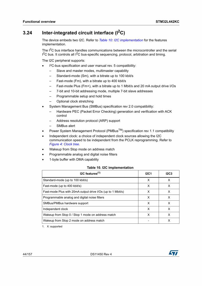
Functional overview STM32L442KC
44/157 DS11450 Rev 4
3.24 Inter-integrated circuit interface (I2C)
The device embeds two I2C. Refer to Table 10: I2C implementation for the features implementation.
The I2C bus interface handles communications between the microcontroller and the serial I2C bus. It controls all I2C bus-specific sequencing, protocol, arbitration and timing.
The I2C peripheral supports:
• I2C-bus specification and user manual rev. 5 compatibility:
– Slave and master modes, multimaster capability
– Standard-mode (Sm), with a bitrate up to 100 kbit/s
– Fast-mode (Fm), with a bitrate up to 400 kbit/s
– Fast-mode Plus (Fm+), with a bitrate up to 1 Mbit/s and 20 mA output drive I/Os
– 7-bit and 10-bit addressing mode, multiple 7-bit slave addresses
– Programmable setup and hold times
– Optional clock stretching
• System Management Bus (SMBus) specification rev 2.0 compatibility:
– Hardware PEC (Packet Error Checking) generation and verification with ACK control
– Address resolution protocol (ARP) support
– SMBus alert
• Power System Management Protocol (PMBusTM) specification rev 1.1 compatibility
• Independent clock: a choice of independent clock sources allowing the I2C communication speed to be independent from the PCLK reprogramming. Refer to Figure 4: Clock tree.
• Wakeup from Stop mode on address match
• Programmable analog and digital noise filters
• 1-byte buffer with DMA capability
Table 10. I2C implementation
I2C features(1)
1. X: supported
I2C1 I2C3
Standard-mode (up to 100 kbit/s) X X
Fast-mode (up to 400 kbit/s) X X
Fast-mode Plus with 20mA output drive I/Os (up to 1 Mbit/s) X X
Programmable analog and digital noise filters X X
SMBus/PMBus hardware support X X
Independent clock X X
Wakeup from Stop 0 / Stop 1 mode on address match X X
Wakeup from Stop 2 mode on address match - X
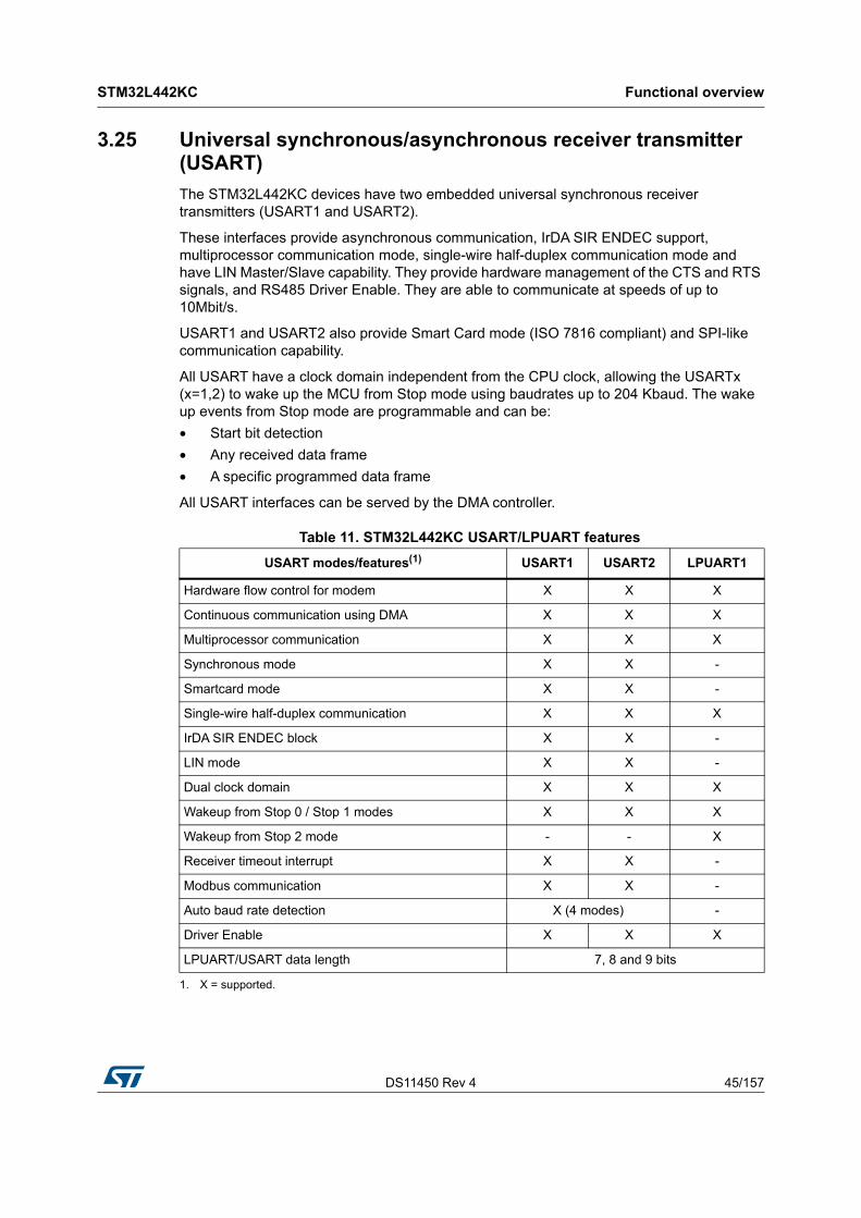
DS11450 Rev 4 45/157
STM32L442KC Functional overview
51
3.25 Universal synchronous/asynchronous receiver transmitter (USART)
The STM32L442KC devices have two embedded universal synchronous receiver transmitters (USART1 and USART2).
These interfaces provide asynchronous communication, IrDA SIR ENDEC support, multiprocessor communication mode, single-wire half-duplex communication mode and have LIN Master/Slave capability. They provide hardware management of the CTS and RTS signals, and RS485 Driver Enable. They are able to communicate at speeds of up to 10Mbit/s.
USART1 and USART2 also provide Smart Card mode (ISO 7816 compliant) and SPI-like communication capability.
All USART have a clock domain independent from the CPU clock, allowing the USARTx (x=1,2) to wake up the MCU from Stop mode using baudrates up to 204 Kbaud. The wake up events from Stop mode are programmable and can be:
• Start bit detection
• Any received data frame
• A specific programmed data frame
All USART interfaces can be served by the DMA controller.
Table 11. STM32L442KC USART/LPUART features
USART modes/features(1)
1. X = supported.
USART1 USART2 LPUART1
Hardware flow control for modem X X X
Continuous communication using DMA X X X
Multiprocessor communication X X X
Synchronous mode X X -
Smartcard mode X X -
Single-wire half-duplex communication X X X
IrDA SIR ENDEC block X X -
LIN mode X X -
Dual clock domain X X X
Wakeup from Stop 0 / Stop 1 modes X X X
Wakeup from Stop 2 mode - - X
Receiver timeout interrupt X X -
Modbus communication X X -
Auto baud rate detection X (4 modes) -
Driver Enable X X X
LPUART/USART data length 7, 8 and 9 bits
Functional overview STM32L442KC
46/157 DS11450 Rev 4
3.26 Low-power universal asynchronous receiver transmitter (LPUART)
The device embeds one Low-Power UART. The LPUART supports asynchronous serial communication with minimum power consumption. It supports half duplex single wire communication and modem operations (CTS/RTS). It allows multiprocessor communication.
The LPUART has a clock domain independent from the CPU clock, and can wakeup the system from Stop mode using baudrates up to 220 Kbaud. The wake up events from Stop mode are programmable and can be:
• Start bit detection
• Any received data frame
• A specific programmed data frame
Only a 32.768 kHz clock (LSE) is needed to allow LPUART communication up to 9600 baud. Therefore, even in Stop mode, the LPUART can wait for an incoming frame while having an extremely low energy consumption. Higher speed clock can be used to reach higher baudrates.
LPUART interface can be served by the DMA controller.
DS11450 Rev 4 47/157
STM32L442KC Functional overview
51
3.27 Serial peripheral interface (SPI)
Two SPI interfaces allow communication up to 40 Mbits/s in master and up to 24 Mbits/s slave modes, in half-duplex, full-duplex and simplex modes. The 3-bit prescaler gives 8 master mode frequencies and the frame size is configurable from 4 bits to 16 bits. The SPI interfaces support NSS pulse mode, TI mode and Hardware CRC calculation.
All SPI interfaces can be served by the DMA controller.
3.28 Serial audio interfaces (SAI)
The device embeds 1 SAI. Refer to Table 12: SAI implementation for the features implementation. The SAI bus interface handles communications between the microcontroller and the serial audio protocol.
The SAI peripheral supports:
• Two independent audio sub-blocks which can be transmitters or receivers with their respective FIFO.
• 8-word integrated FIFOs for each audio sub-block.
• Synchronous or asynchronous mode between the audio sub-blocks.
• Master or slave configuration independent for both audio sub-blocks.
• Clock generator for each audio block to target independent audio frequency sampling when both audio sub-blocks are configured in master mode.
• Data size configurable: 8-, 10-, 16-, 20-, 24-, 32-bit.
• Peripheral with large configurability and flexibility allowing to target as example the following audio protocol: I2S, LSB or MSB-justified, PCM/DSP, TDM, AC’97 and SPDIF out.
• Up to 16 slots available with configurable size and with the possibility to select which ones are active in the audio frame.
• Number of bits by frame may be configurable.
• Frame synchronization active level configurable (offset, bit length, level).
• First active bit position in the slot is configurable.
• LSB first or MSB first for data transfer.
• Mute mode.
• Stereo/Mono audio frame capability.
• Communication clock strobing edge configurable (SCK).
• Error flags with associated interrupts if enabled respectively.
– Overrun and underrun detection.
– Anticipated frame synchronization signal detection in slave mode.
– Late frame synchronization signal detection in slave mode.
– Codec not ready for the AC’97 mode in reception.
• Interruption sources when enabled:
– Errors.
– FIFO requests.
• DMA interface with 2 dedicated channels to handle access to the dedicated integrated FIFO of each SAI audio sub-block.
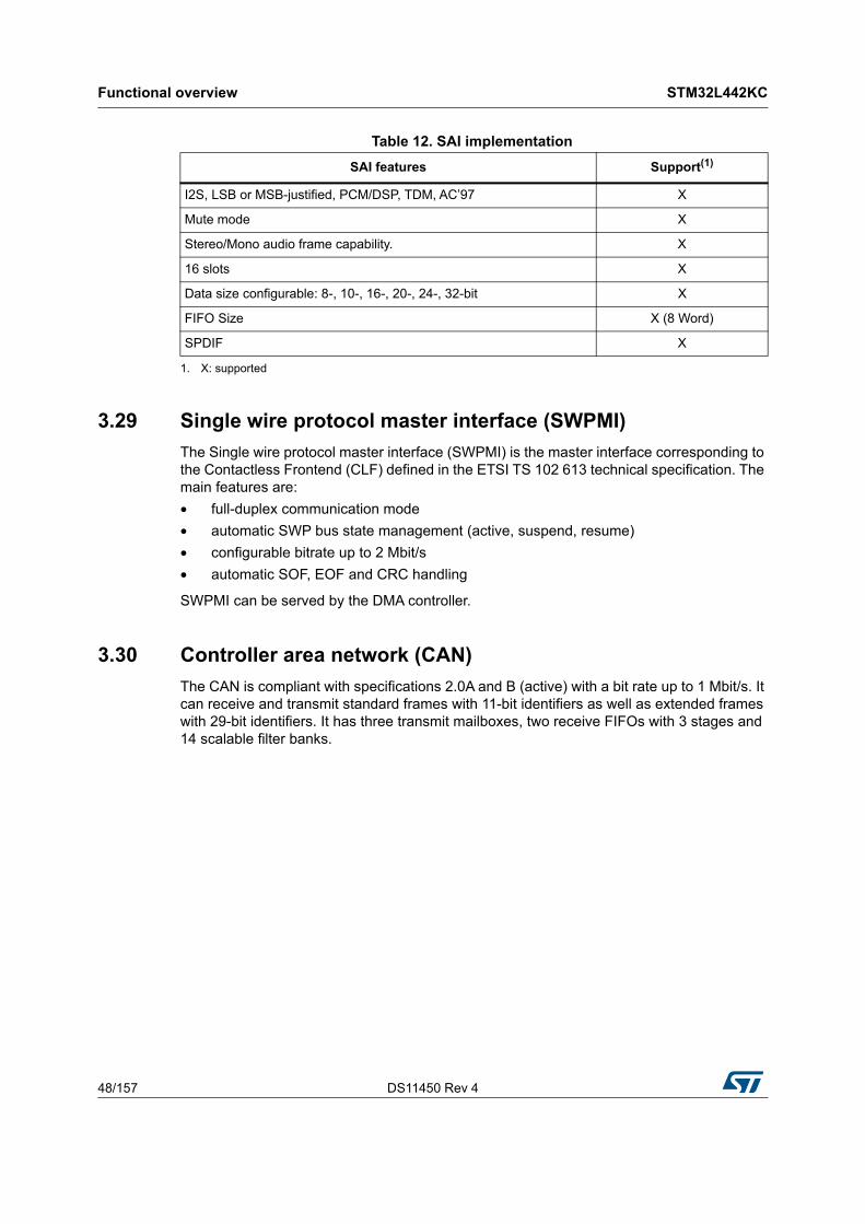
Functional overview STM32L442KC
48/157 DS11450 Rev 4
3.29 Single wire protocol master interface (SWPMI)
The Single wire protocol master interface (SWPMI) is the master interface corresponding to the Contactless Frontend (CLF) defined in the ETSI TS 102 613 technical specification. The main features are:
• full-duplex communication mode
• automatic SWP bus state management (active, suspend, resume)
• configurable bitrate up to 2 Mbit/s
• automatic SOF, EOF and CRC handling
SWPMI can be served by the DMA controller.
3.30 Controller area network (CAN)
The CAN is compliant with specifications 2.0A and B (active) with a bit rate up to 1 Mbit/s. It can receive and transmit standard frames with 11-bit identifiers as well as extended frames with 29-bit identifiers. It has three transmit mailboxes, two receive FIFOs with 3 stages and 14 scalable filter banks.
Table 12. SAI implementation
SAI features Support(1)
1. X: supported
I2S, LSB or MSB-justified, PCM/DSP, TDM, AC’97 X
Mute mode X
Stereo/Mono audio frame capability. X
16 slots X
Data size configurable: 8-, 10-, 16-, 20-, 24-, 32-bit X
FIFO Size X (8 Word)
SPDIF X
DS11450 Rev 4 49/157
STM32L442KC Functional overview
51
The CAN peripheral supports:
• Supports CAN protocol version 2.0 A, B Active
• Bit rates up to 1 Mbit/s
• Transmission
– Three transmit mailboxes
– Configurable transmit priority
• Reception
– Two receive FIFOs with three stages
– 14 Scalable filter banks
– Identifier list feature
– Configurable FIFO overrun
• Time-triggered communication option
– Disable automatic retransmission mode
– 16-bit free running timer
– Time Stamp sent in last two data bytes
• Management
– Maskable interrupts
– Software-efficient mailbox mapping at a unique address space
3.31 Universal serial bus (USB)
The STM32L442KC devices embed a full-speed USB device peripheral compliant with the USB specification version 2.0. The internal USB PHY supports USB FS signaling, embedded DP pull-up and also battery charging detection according to Battery Charging Specification Revision 1.2. The USB interface implements a full-speed (12 Mbit/s) function interface with added support for USB 2.0 Link Power Management. It has software-configurable endpoint setting with packet memory up-to 1 KB and suspend/resume support. It requires a precise 48 MHz clock which can be generated from the internal main PLL or by the internal 48 MHz oscillator in automatic trimming mode. The synchronization for this oscillator can be taken from the USB data stream itself (SOF signalization) which allows crystal less operation.
3.32 Clock recovery system (CRS)
The STM32L442KC devices embed a special block which allows automatic trimming of the internal 48 MHz oscillator to guarantee its optimal accuracy over the whole device operational range. This automatic trimming is based on the external synchronization signal, which could be either derived from USB SOF signalization, from LSE oscillator, from an external signal on CRS_SYNC pin or generated by user software. For faster lock-in during startup it is also possible to combine automatic trimming with manual trimming action.
Functional overview STM32L442KC
50/157 DS11450 Rev 4
3.33 Quad SPI memory interface (QUADSPI)
The Quad SPI is a specialized communication interface targeting single, dual or quad SPI flash memories. It can operate in any of the three following modes:
• Indirect mode: all the operations are performed using the QUADSPI registers
• Status polling mode: the external flash status register is periodically read and an interrupt can be generated in case of flag setting
• Memory-mapped mode: the external Flash is memory mapped and is seen by the system as if it were an internal memory
Both throughput and capacity can be increased two-fold using dual-flash mode, where two Quad SPI flash memories are accessed simultaneously.
The Quad SPI interface supports:
• Three functional modes: indirect, status-polling, and memory-mapped
• SDR and DDR support
• Fully programmable opcode for both indirect and memory mapped mode
• Fully programmable frame format for both indirect and memory mapped mode
• Each of the 5 following phases can be configured independently (enable, length, single/dual/quad communication)
– Instruction phase
– Address phase
– Alternate bytes phase
– Dummy cycles phase
– Data phase
• Integrated FIFO for reception and transmission
• 8, 16, and 32-bit data accesses are allowed
• DMA channel for indirect mode operations
• Programmable masking for external flash flag management
• Timeout management
• Interrupt generation on FIFO threshold, timeout, status match, operation complete, and access error

DS11450 Rev 4 51/157
STM32L442KC Functional overview
51
3.34 Development support
3.34.1 Serial wire JTAG debug port (SWJ-DP)
The Arm® SWJ-DP interface is embedded, and is a combined JTAG and serial wire debug port that enables either a serial wire debug or a JTAG probe to be connected to the target.
Debug is performed using 2 pins only instead of 5 required by the JTAG (JTAG pins could be re-use as GPIO with alternate function): the JTAG TMS and TCK pins are shared with SWDIO and SWCLK, respectively, and a specific sequence on the TMS pin is used to switch between JTAG-DP and SW-DP.
3.34.2 Embedded Trace Macrocell™
The Arm® Embedded Trace Macrocell™ provides a greater visibility of the instruction and data flow inside the CPU core by streaming compressed data at a very high rate from the STM32L442KC through a small number of ETM pins to an external hardware trace port analyzer (TPA) device. Real-time instruction and data flow activity be recorded and then formatted for display on the host computer that runs the debugger software. TPA hardware is commercially available from common development tool vendors.
The Embedded Trace Macrocell™ operates with third party debugger software tools.
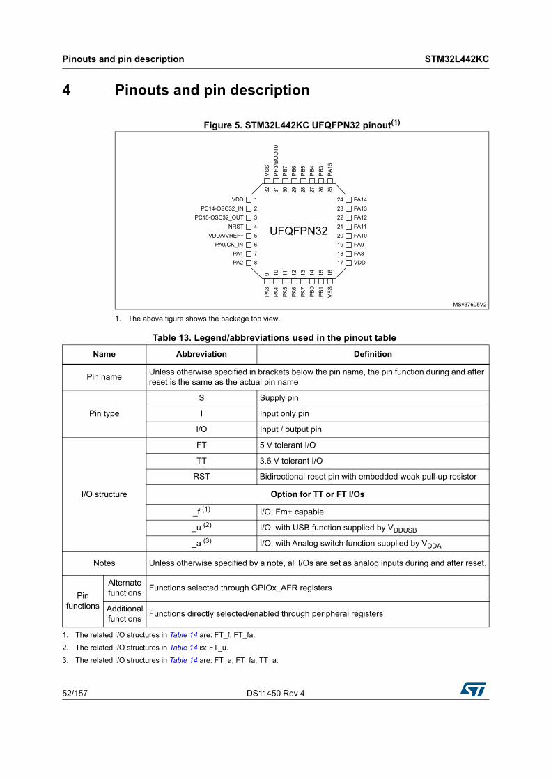
Pinouts and pin description STM32L442KC
52/157 DS11450 Rev 4
4 Pinouts and pin description
Figure 5. STM32L442KC UFQFPN32 pinout(1)
1. The above figure shows the package top view.
MSv37605V2
UFQFPN32
12345678
VDDPC14-OSC32_IN
PC15-OSC32_OUTNRST
VDDA/VREF+PA0/CK_IN
PA1PA2
2423222120191817
29 27 2532 31 30 28 26
12 14 169 10 11 13 15
PA3
PA4
PA7
VS
S
PA5
PA6
PB
0P
B1
PA14PA13PA12PA11PA10PA9PA8VDD
VS
SP
H3/
BO
OT0
PB
5
PA15
PB
7P
B6
PB
4P
B3
Table 13. Legend/abbreviations used in the pinout table
Name Abbreviation Definition
Pin nameUnless otherwise specified in brackets below the pin name, the pin function during and after reset is the same as the actual pin name
Pin type
S Supply pin
I Input only pin
I/O Input / output pin
I/O structure
FT 5 V tolerant I/O
TT 3.6 V tolerant I/O
RST Bidirectional reset pin with embedded weak pull-up resistor
Option for TT or FT I/Os
_f (1) I/O, Fm+ capable
_u (2) I/O, with USB function supplied by VDDUSB
_a (3) I/O, with Analog switch function supplied by VDDA
Notes Unless otherwise specified by a note, all I/Os are set as analog inputs during and after reset.
Pin functions
Alternate functions
Functions selected through GPIOx_AFR registers
Additional functions
Functions directly selected/enabled through peripheral registers
1. The related I/O structures in Table 14 are: FT_f, FT_fa.
2. The related I/O structures in Table 14 is: FT_u.
3. The related I/O structures in Table 14 are: FT_a, FT_fa, TT_a.
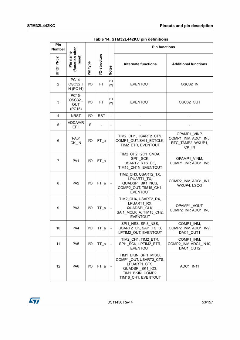
DS11450 Rev 4 53/157
STM32L442KC Pinouts and pin description
63
Table 14. STM32L442KC pin definitions Pin
Number
Pin
nam
e(f
un
ctio
n a
fter
res
et)
Pin
typ
e
I/O s
tru
ctu
re
No
tes
Pin functions
UF
QF
PN
32
Alternate functions Additional functions
2PC14-
OSC32_IN (PC14)
I/O FT(1)
(2) EVENTOUT OSC32_IN
3
PC15-OSC32_
OUT (PC15)
I/O FT(1)
(2) EVENTOUT OSC32_OUT
4 NRST I/O RST - - -
5VDDA/VR
EF+S - - - -
6PA0/
CK_INI/O FT_a -
TIM2_CH1, USART2_CTS, COMP1_OUT, SAI1_EXTCLK,
TIM2_ETR, EVENTOUT
OPAMP1_VINP, COMP1_INM, ADC1_IN5,
RTC_TAMP2, WKUP1, CK_IN
7 PA1 I/O FT_a -
TIM2_CH2, I2C1_SMBA, SPI1_SCK,
USART2_RTS_DE, TIM15_CH1N, EVENTOUT
OPAMP1_VINM, COMP1_INP, ADC1_IN6
8 PA2 I/O FT_a -
TIM2_CH3, USART2_TX, LPUART1_TX,
QUADSPI_BK1_NCS, COMP2_OUT, TIM15_CH1,
EVENTOUT
COMP2_INM, ADC1_IN7, WKUP4, LSCO
9 PA3 I/O TT_a -
TIM2_CH4, USART2_RX, LPUART1_RX,
QUADSPI_CLK, SAI1_MCLK_A, TIM15_CH2,
EVENTOUT
OPAMP1_VOUT, COMP2_INP, ADC1_IN8
10 PA4 I/O TT_a -SPI1_NSS, SPI3_NSS,
USART2_CK, SAI1_FS_B, LPTIM2_OUT, EVENTOUT
COMP1_INM, COMP2_INM, ADC1_IN9,
DAC1_OUT1
11 PA5 I/O TT_a -TIM2_CH1, TIM2_ETR,
SPI1_SCK, LPTIM2_ETR, EVENTOUT
COMP1_INM, COMP2_INM, ADC1_IN10,
DAC1_OUT2
12 PA6 I/O FT_a -
TIM1_BKIN, SPI1_MISO, COMP1_OUT, USART3_CTS,
LPUART1_CTS, QUADSPI_BK1_IO3, TIM1_BKIN_COMP2,
TIM16_CH1, EVENTOUT
ADC1_IN11
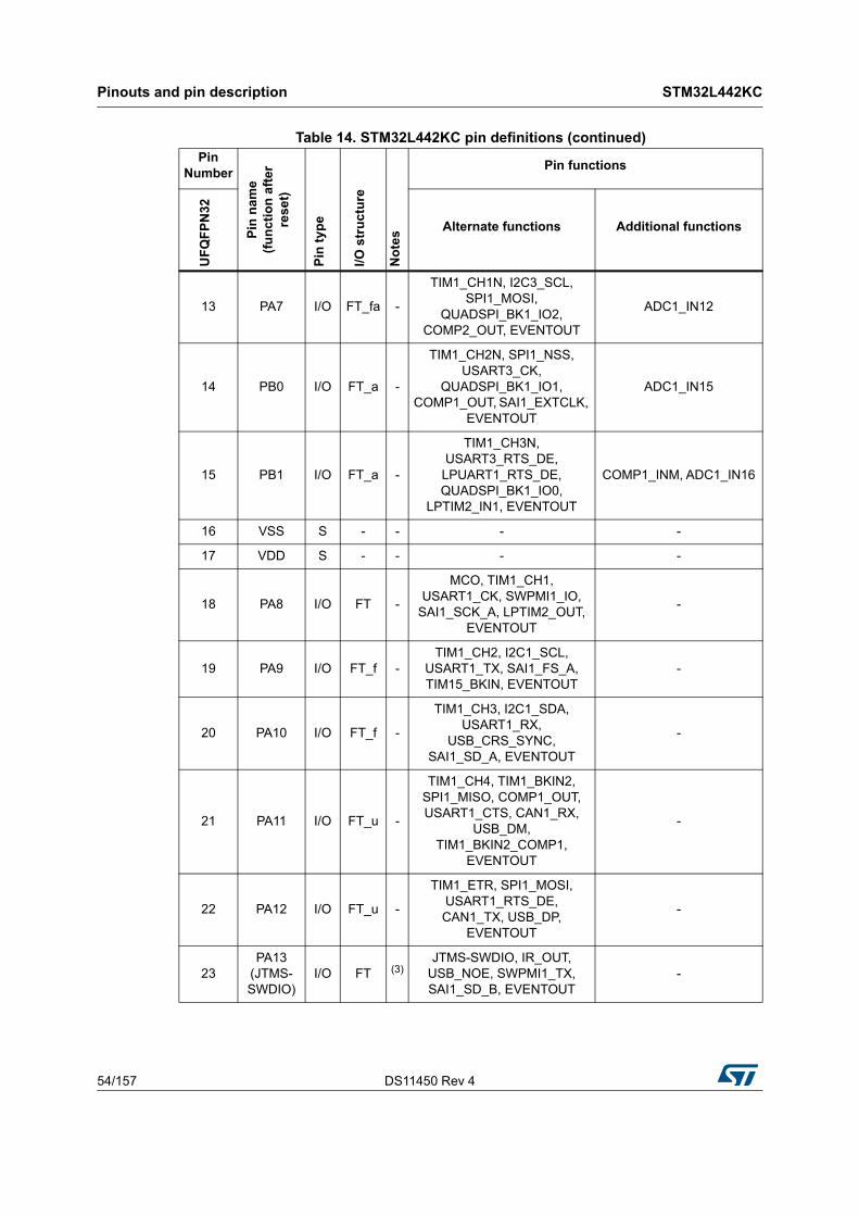
Pinouts and pin description STM32L442KC
54/157 DS11450 Rev 4
13 PA7 I/O FT_fa -
TIM1_CH1N, I2C3_SCL, SPI1_MOSI,
QUADSPI_BK1_IO2, COMP2_OUT, EVENTOUT
ADC1_IN12
14 PB0 I/O FT_a -
TIM1_CH2N, SPI1_NSS, USART3_CK,
QUADSPI_BK1_IO1, COMP1_OUT, SAI1_EXTCLK,
EVENTOUT
ADC1_IN15
15 PB1 I/O FT_a -
TIM1_CH3N, USART3_RTS_DE,
LPUART1_RTS_DE, QUADSPI_BK1_IO0,
LPTIM2_IN1, EVENTOUT
COMP1_INM, ADC1_IN16
16 VSS S - - - -
17 VDD S - - - -
18 PA8 I/O FT -
MCO, TIM1_CH1, USART1_CK, SWPMI1_IO,
SAI1_SCK_A, LPTIM2_OUT, EVENTOUT
-
19 PA9 I/O FT_f -TIM1_CH2, I2C1_SCL,
USART1_TX, SAI1_FS_A, TIM15_BKIN, EVENTOUT
-
20 PA10 I/O FT_f -
TIM1_CH3, I2C1_SDA, USART1_RX,
USB_CRS_SYNC, SAI1_SD_A, EVENTOUT
-
21 PA11 I/O FT_u -
TIM1_CH4, TIM1_BKIN2, SPI1_MISO, COMP1_OUT, USART1_CTS, CAN1_RX,
USB_DM, TIM1_BKIN2_COMP1,
EVENTOUT
-
22 PA12 I/O FT_u -
TIM1_ETR, SPI1_MOSI, USART1_RTS_DE, CAN1_TX, USB_DP,
EVENTOUT
-
23PA13
(JTMS-SWDIO)
I/O FT (3)JTMS-SWDIO, IR_OUT,
USB_NOE, SWPMI1_TX, SAI1_SD_B, EVENTOUT
-
Table 14. STM32L442KC pin definitions (continued)Pin
Number
Pin
na
me
(fu
nct
ion
aft
erre
set)
Pin
typ
e
I/O s
tru
ctu
re
No
tes
Pin functions
UF
QF
PN
32
Alternate functions Additional functions
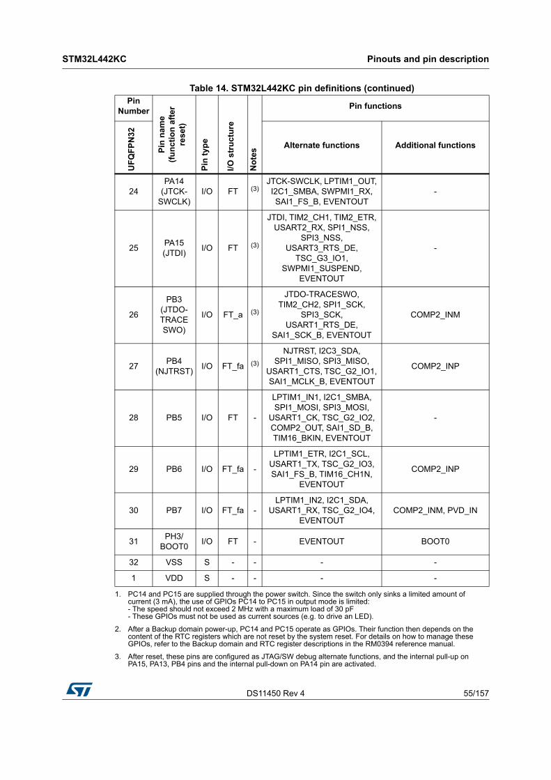
DS11450 Rev 4 55/157
STM32L442KC Pinouts and pin description
63
24PA14
(JTCK-SWCLK)
I/O FT (3)JTCK-SWCLK, LPTIM1_OUT, I2C1_SMBA, SWPMI1_RX, SAI1_FS_B, EVENTOUT
-
25PA15 (JTDI)
I/O FT (3)
JTDI, TIM2_CH1, TIM2_ETR, USART2_RX, SPI1_NSS,
SPI3_NSS, USART3_RTS_DE,
TSC_G3_IO1, SWPMI1_SUSPEND,
EVENTOUT
-
26
PB3 (JTDO-TRACESWO)
I/O FT_a (3)
JTDO-TRACESWO, TIM2_CH2, SPI1_SCK,
SPI3_SCK, USART1_RTS_DE,
SAI1_SCK_B, EVENTOUT
COMP2_INM
27PB4
(NJTRST)I/O FT_fa (3)
NJTRST, I2C3_SDA, SPI1_MISO, SPI3_MISO,
USART1_CTS, TSC_G2_IO1, SAI1_MCLK_B, EVENTOUT
COMP2_INP
28 PB5 I/O FT -
LPTIM1_IN1, I2C1_SMBA, SPI1_MOSI, SPI3_MOSI,
USART1_CK, TSC_G2_IO2, COMP2_OUT, SAI1_SD_B, TIM16_BKIN, EVENTOUT
-
29 PB6 I/O FT_fa -
LPTIM1_ETR, I2C1_SCL, USART1_TX, TSC_G2_IO3, SAI1_FS_B, TIM16_CH1N,
EVENTOUT
COMP2_INP
30 PB7 I/O FT_fa -LPTIM1_IN2, I2C1_SDA,
USART1_RX, TSC_G2_IO4, EVENTOUT
COMP2_INM, PVD_IN
31PH3/
BOOT0I/O FT - EVENTOUT BOOT0
32 VSS S - - - -
1 VDD S - - - -
1. PC14 and PC15 are supplied through the power switch. Since the switch only sinks a limited amount of current (3 mA), the use of GPIOs PC14 to PC15 in output mode is limited: - The speed should not exceed 2 MHz with a maximum load of 30 pF - These GPIOs must not be used as current sources (e.g. to drive an LED).
2. After a Backup domain power-up, PC14 and PC15 operate as GPIOs. Their function then depends on the content of the RTC registers which are not reset by the system reset. For details on how to manage these GPIOs, refer to the Backup domain and RTC register descriptions in the RM0394 reference manual.
3. After reset, these pins are configured as JTAG/SW debug alternate functions, and the internal pull-up on PA15, PA13, PB4 pins and the internal pull-down on PA14 pin are activated.
Table 14. STM32L442KC pin definitions (continued)Pin
Number
Pin
na
me
(fu
nct
ion
aft
erre
set)
Pin
typ
e
I/O s
tru
ctu
re
No
tes
Pin functions
UF
QF
PN
32
Alternate functions Additional functions
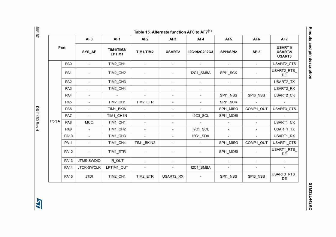
Pin
ou
ts a
nd
pin
de
scrip
tion
ST
M3
2L
44
2KC
56/1
57D
S114
50 Rev 4
Table 15. Alternate function AF0 to AF7(1)
Port
AF0 AF1 AF2 AF3 AF4 AF5 AF6 AF7
SYS_AFTIM1/TIM2/
LPTIM1TIM1/TIM2 USART2 I2C1/I2C2/I2C3 SPI1/SPI2 SPI3
USART1/USART2/USART3
Port A
PA0 - TIM2_CH1 - - - - - USART2_CTS
PA1 - TIM2_CH2 - - I2C1_SMBA SPI1_SCK -USART2_RTS_
DE
PA2 - TIM2_CH3 - - - - - USART2_TX
PA3 - TIM2_CH4 - - - - - USART2_RX
PA4 - - - - - SPI1_NSS SPI3_NSS USART2_CK
PA5 - TIM2_CH1 TIM2_ETR - - SPI1_SCK - -
PA6 - TIM1_BKIN - - - SPI1_MISO COMP1_OUT USART3_CTS
PA7 - TIM1_CH1N - - I2C3_SCL SPI1_MOSI - -
PA8 MCO TIM1_CH1 - - - - - USART1_CK
PA9 - TIM1_CH2 - - I2C1_SCL - - USART1_TX
PA10 - TIM1_CH3 - - I2C1_SDA - - USART1_RX
PA11 - TIM1_CH4 TIM1_BKIN2 - - SPI1_MISO COMP1_OUT USART1_CTS
PA12 - TIM1_ETR - - - SPI1_MOSI -USART1_RTS_
DE
PA13 JTMS-SWDIO IR_OUT - - - - - -
PA14 JTCK-SWCLK LPTIM1_OUT - - I2C1_SMBA - - -
PA15 JTDI TIM2_CH1 TIM2_ETR USART2_RX - SPI1_NSS SPI3_NSSUSART3_RTS_
DE
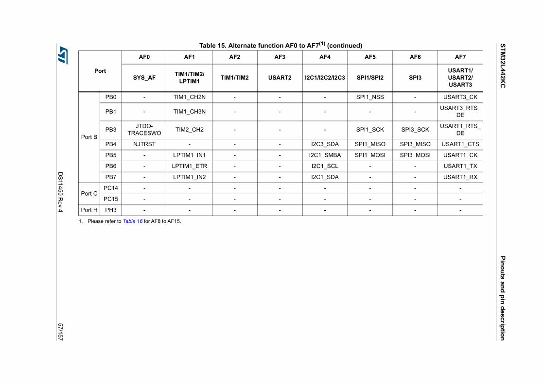
ST
M3
2L4
42K
CP
ino
uts
an
d p
in d
esc
riptio
n
DS
11450 R
ev 457/157
Port B
PB0 - TIM1_CH2N - - - SPI1_NSS - USART3_CK
PB1 - TIM1_CH3N - - - - -USART3_RTS_
DE
PB3JTDO-
TRACESWOTIM2_CH2 - - - SPI1_SCK SPI3_SCK
USART1_RTS_DE
PB4 NJTRST - - - I2C3_SDA SPI1_MISO SPI3_MISO USART1_CTS
PB5 - LPTIM1_IN1 - - I2C1_SMBA SPI1_MOSI SPI3_MOSI USART1_CK
PB6 - LPTIM1_ETR - - I2C1_SCL - - USART1_TX
PB7 - LPTIM1_IN2 - - I2C1_SDA - - USART1_RX
Port CPC14 - - - - - - - -
PC15 - - - - - - - -
Port H PH3 - - - - - - - -
1. Please refer to Table 16 for AF8 to AF15.
Table 15. Alternate function AF0 to AF7(1) (continued)
Port
AF0 AF1 AF2 AF3 AF4 AF5 AF6 AF7
SYS_AFTIM1/TIM2/
LPTIM1TIM1/TIM2 USART2 I2C1/I2C2/I2C3 SPI1/SPI2 SPI3
USART1/USART2/USART3

Pin
ou
ts a
nd
pin
de
scrip
tion
ST
M3
2L
44
2KC
58/1
57D
S114
50 Rev 4
Table 16. Alternate function AF8 to AF15(1)
Port
AF8 AF9 AF10 AF11 AF12 AF13 AF14 AF15
LPUART1 CAN1/TSC USB/QUADSPI -COMP1/COMP2/SWPMI1
SAI1TIM2/TIM15/
TIM16/LPTIM2EVENTOUT
Port A
PA0 - - - - COMP1_OUT SAI1_EXTCLK TIM2_ETR EVENTOUT
PA1 - - - - - - TIM15_CH1N EVENTOUT
PA2 LPUART1_TX -QUADSPI_BK1_NCS
- COMP2_OUT - TIM15_CH1 EVENTOUT
PA3 LPUART1_RX - QUADSPI_CLK - - SAI1_MCLK_A TIM15_CH2 EVENTOUT
PA4 - - - - - SAI1_FS_B LPTIM2_OUT EVENTOUT
PA5 - - - - - - LPTIM2_ETR EVENTOUT
PA6 LPUART1_CTS -QUADSPI_BK1_IO3
-TIM1_BKIN_
COMP2- TIM16_CH1 EVENTOUT
PA7 - -QUADSPI_BK1_IO2
- COMP2_OUT - - EVENTOUT
PA8 - - - - SWPMI1_IO SAI1_SCK_A LPTIM2_OUT EVENTOUT
PA9 - - - - - SAI1_FS_A TIM15_BKIN EVENTOUT
PA10 - -USB_CRS_
SYNC- - SAI1_SD_A - EVENTOUT
PA11 - CAN1_RX USB_DM -TIM1_BKIN2_
COMP1- - EVENTOUT
PA12 - CAN1_TX USB_DP - - - - EVENTOUT
PA13 - - USB_NOE - SWPMI1_TX SAI1_SD_B - EVENTOUT
PA14 - - - - SWPMI1_RX SAI1_FS_B - EVENTOUT
PA15 - TSC_G3_IO1 - -SWPMI1_SUSPEND
- - EVENTOUT
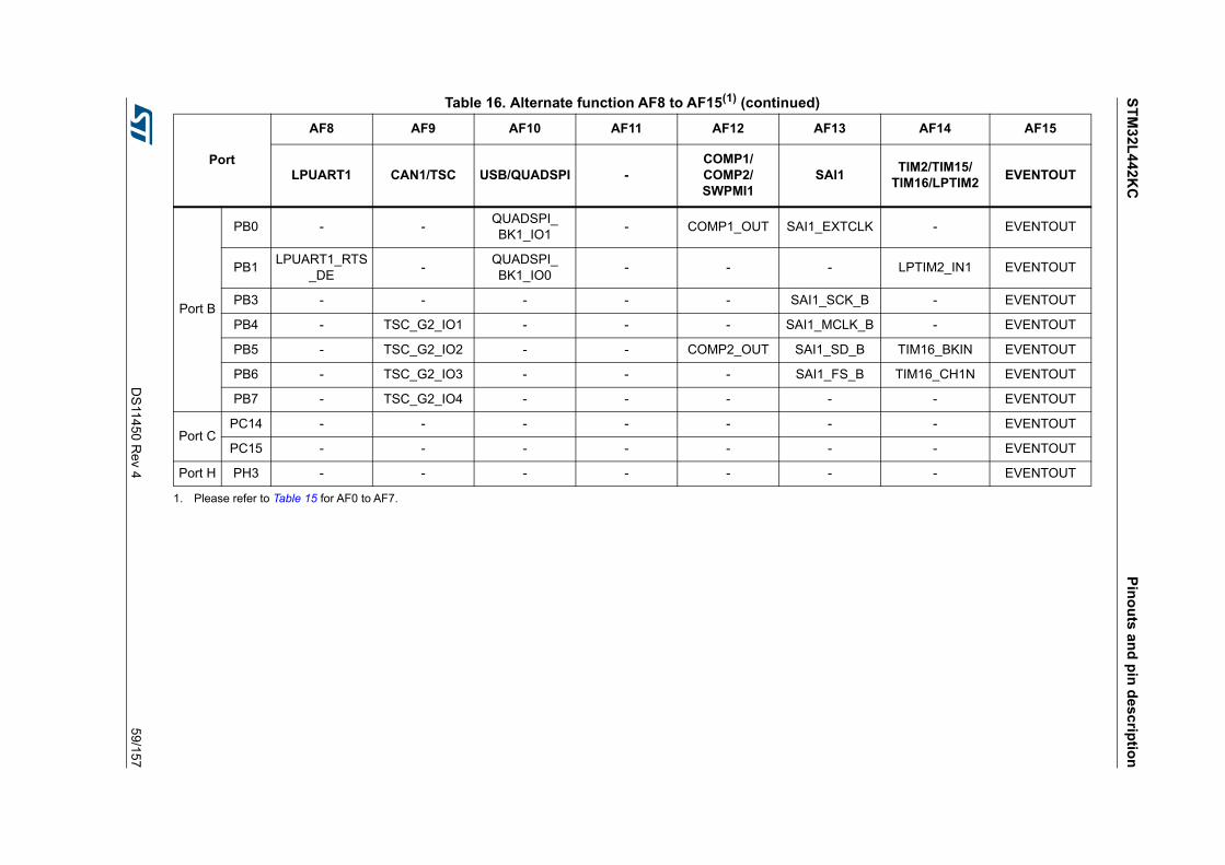
ST
M3
2L4
42K
CP
ino
uts
an
d p
in d
esc
riptio
n
DS
11450 R
ev 459/157
Port B
PB0 - -QUADSPI_BK1_IO1
- COMP1_OUT SAI1_EXTCLK - EVENTOUT
PB1LPUART1_RTS
_DE-
QUADSPI_BK1_IO0
- - - LPTIM2_IN1 EVENTOUT
PB3 - - - - - SAI1_SCK_B - EVENTOUT
PB4 - TSC_G2_IO1 - - - SAI1_MCLK_B - EVENTOUT
PB5 - TSC_G2_IO2 - - COMP2_OUT SAI1_SD_B TIM16_BKIN EVENTOUT
PB6 - TSC_G2_IO3 - - - SAI1_FS_B TIM16_CH1N EVENTOUT
PB7 - TSC_G2_IO4 - - - - - EVENTOUT
Port CPC14 - - - - - - - EVENTOUT
PC15 - - - - - - - EVENTOUT
Port H PH3 - - - - - - - EVENTOUT
1. Please refer to Table 15 for AF0 to AF7.
Table 16. Alternate function AF8 to AF15(1) (continued)
Port
AF8 AF9 AF10 AF11 AF12 AF13 AF14 AF15
LPUART1 CAN1/TSC USB/QUADSPI -COMP1/COMP2/SWPMI1
SAI1TIM2/TIM15/
TIM16/LPTIM2EVENTOUT
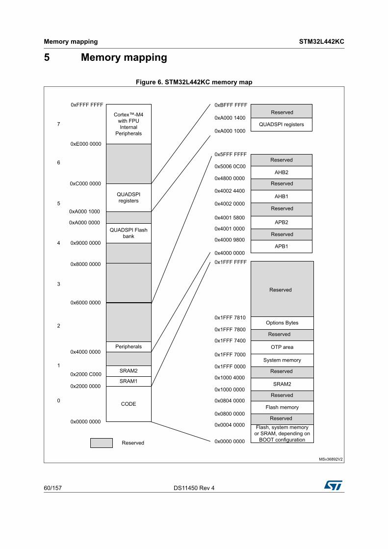
Memory mapping STM32L442KC
60/157 DS11450 Rev 4
5 Memory mapping
Figure 6. STM32L442KC memory map
MSv36892V2
0xFFFF FFFF
0xE000 0000
0xC000 0000
0xA000 1000
0x8000 0000
0x6000 0000
0x4000 0000
0x2000 0000
0x0000 0000
0
1
2
3
4
5
6
7
Cortex™-M4with FPU Internal
Peripherals
Peripherals
SRAM1
CODE
OTP area
System memory
Flash memory
Flash, system memory or SRAM, depending on
BOOT configuration
AHB2
AHB1
APB2
APB1
0x5006 0C00
0x4800 0000
0x4002 4400
0x4002 0000
0x4001 5800
0x4001 0000
0x4000 9800
0x4000 0000
0x1FFF FFFF
0x1FFF 0000
0x0804 0000
0x0800 0000
0x0004 0000
0x0000 0000Reserved
Reserved
Reserved
Reserved
Reserved
Reserved
Reserved0x1000 4000
0x1000 0000SRAM2
QUADSPI registers
Options Bytes
0x1FFF 7000
0x1FFF 7400
0x1FFF 7800
0x1FFF 7810
Reserved
QUADSPI registers
0xBFFF FFFF
0xA000 1400
0xA000 1000
Reserved
Reserved
Reserved0x5FFF FFFF
0x9000 0000
QUADSPI Flash bank
SRAM20x2000 C000
0xA000 0000
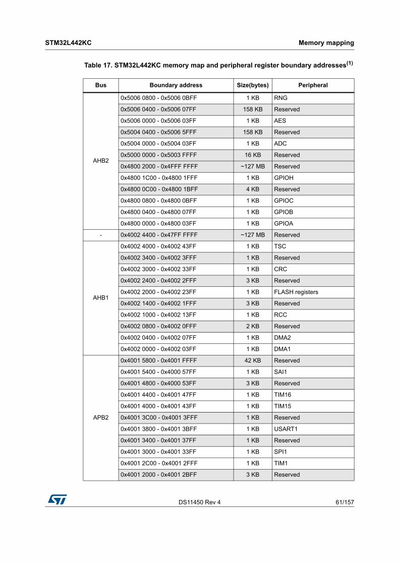
DS11450 Rev 4 61/157
STM32L442KC Memory mapping
63
Table 17. STM32L442KC memory map and peripheral register boundary addresses(1)
Bus Boundary address Size(bytes) Peripheral
AHB2
0x5006 0800 - 0x5006 0BFF 1 KB RNG
0x5006 0400 - 0x5006 07FF 158 KB Reserved
0x5006 0000 - 0x5006 03FF 1 KB AES
0x5004 0400 - 0x5006 5FFF 158 KB Reserved
0x5004 0000 - 0x5004 03FF 1 KB ADC
0x5000 0000 - 0x5003 FFFF 16 KB Reserved
0x4800 2000 - 0x4FFF FFFF ~127 MB Reserved
0x4800 1C00 - 0x4800 1FFF 1 KB GPIOH
0x4800 0C00 - 0x4800 1BFF 4 KB Reserved
0x4800 0800 - 0x4800 0BFF 1 KB GPIOC
0x4800 0400 - 0x4800 07FF 1 KB GPIOB
0x4800 0000 - 0x4800 03FF 1 KB GPIOA
- 0x4002 4400 - 0x47FF FFFF ~127 MB Reserved
AHB1
0x4002 4000 - 0x4002 43FF 1 KB TSC
0x4002 3400 - 0x4002 3FFF 1 KB Reserved
0x4002 3000 - 0x4002 33FF 1 KB CRC
0x4002 2400 - 0x4002 2FFF 3 KB Reserved
0x4002 2000 - 0x4002 23FF 1 KB FLASH registers
0x4002 1400 - 0x4002 1FFF 3 KB Reserved
0x4002 1000 - 0x4002 13FF 1 KB RCC
0x4002 0800 - 0x4002 0FFF 2 KB Reserved
0x4002 0400 - 0x4002 07FF 1 KB DMA2
0x4002 0000 - 0x4002 03FF 1 KB DMA1
APB2
0x4001 5800 - 0x4001 FFFF 42 KB Reserved
0x4001 5400 - 0x4000 57FF 1 KB SAI1
0x4001 4800 - 0x4000 53FF 3 KB Reserved
0x4001 4400 - 0x4001 47FF 1 KB TIM16
0x4001 4000 - 0x4001 43FF 1 KB TIM15
0x4001 3C00 - 0x4001 3FFF 1 KB Reserved
0x4001 3800 - 0x4001 3BFF 1 KB USART1
0x4001 3400 - 0x4001 37FF 1 KB Reserved
0x4001 3000 - 0x4001 33FF 1 KB SPI1
0x4001 2C00 - 0x4001 2FFF 1 KB TIM1
0x4001 2000 - 0x4001 2BFF 3 KB Reserved
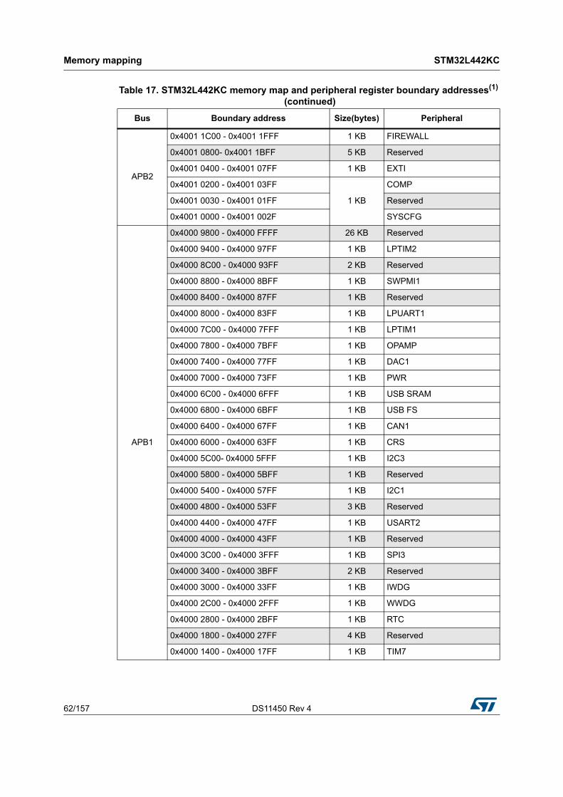
Memory mapping STM32L442KC
62/157 DS11450 Rev 4
APB2
0x4001 1C00 - 0x4001 1FFF 1 KB FIREWALL
0x4001 0800- 0x4001 1BFF 5 KB Reserved
0x4001 0400 - 0x4001 07FF 1 KB EXTI
0x4001 0200 - 0x4001 03FF
1 KB
COMP
0x4001 0030 - 0x4001 01FF Reserved
0x4001 0000 - 0x4001 002F SYSCFG
APB1
0x4000 9800 - 0x4000 FFFF 26 KB Reserved
0x4000 9400 - 0x4000 97FF 1 KB LPTIM2
0x4000 8C00 - 0x4000 93FF 2 KB Reserved
0x4000 8800 - 0x4000 8BFF 1 KB SWPMI1
0x4000 8400 - 0x4000 87FF 1 KB Reserved
0x4000 8000 - 0x4000 83FF 1 KB LPUART1
0x4000 7C00 - 0x4000 7FFF 1 KB LPTIM1
0x4000 7800 - 0x4000 7BFF 1 KB OPAMP
0x4000 7400 - 0x4000 77FF 1 KB DAC1
0x4000 7000 - 0x4000 73FF 1 KB PWR
0x4000 6C00 - 0x4000 6FFF 1 KB USB SRAM
0x4000 6800 - 0x4000 6BFF 1 KB USB FS
0x4000 6400 - 0x4000 67FF 1 KB CAN1
0x4000 6000 - 0x4000 63FF 1 KB CRS
0x4000 5C00- 0x4000 5FFF 1 KB I2C3
0x4000 5800 - 0x4000 5BFF 1 KB Reserved
0x4000 5400 - 0x4000 57FF 1 KB I2C1
0x4000 4800 - 0x4000 53FF 3 KB Reserved
0x4000 4400 - 0x4000 47FF 1 KB USART2
0x4000 4000 - 0x4000 43FF 1 KB Reserved
0x4000 3C00 - 0x4000 3FFF 1 KB SPI3
0x4000 3400 - 0x4000 3BFF 2 KB Reserved
0x4000 3000 - 0x4000 33FF 1 KB IWDG
0x4000 2C00 - 0x4000 2FFF 1 KB WWDG
0x4000 2800 - 0x4000 2BFF 1 KB RTC
0x4000 1800 - 0x4000 27FF 4 KB Reserved
0x4000 1400 - 0x4000 17FF 1 KB TIM7
Table 17. STM32L442KC memory map and peripheral register boundary addresses(1)
(continued)
Bus Boundary address Size(bytes) Peripheral
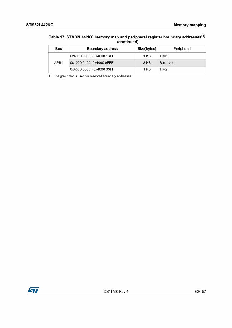
DS11450 Rev 4 63/157
STM32L442KC Memory mapping
63
APB1
0x4000 1000 - 0x4000 13FF 1 KB TIM6
0x4000 0400- 0x4000 0FFF 3 KB Reserved
0x4000 0000 - 0x4000 03FF 1 KB TIM2
1. The gray color is used for reserved boundary addresses.
Table 17. STM32L442KC memory map and peripheral register boundary addresses(1)
(continued)
Bus Boundary address Size(bytes) Peripheral
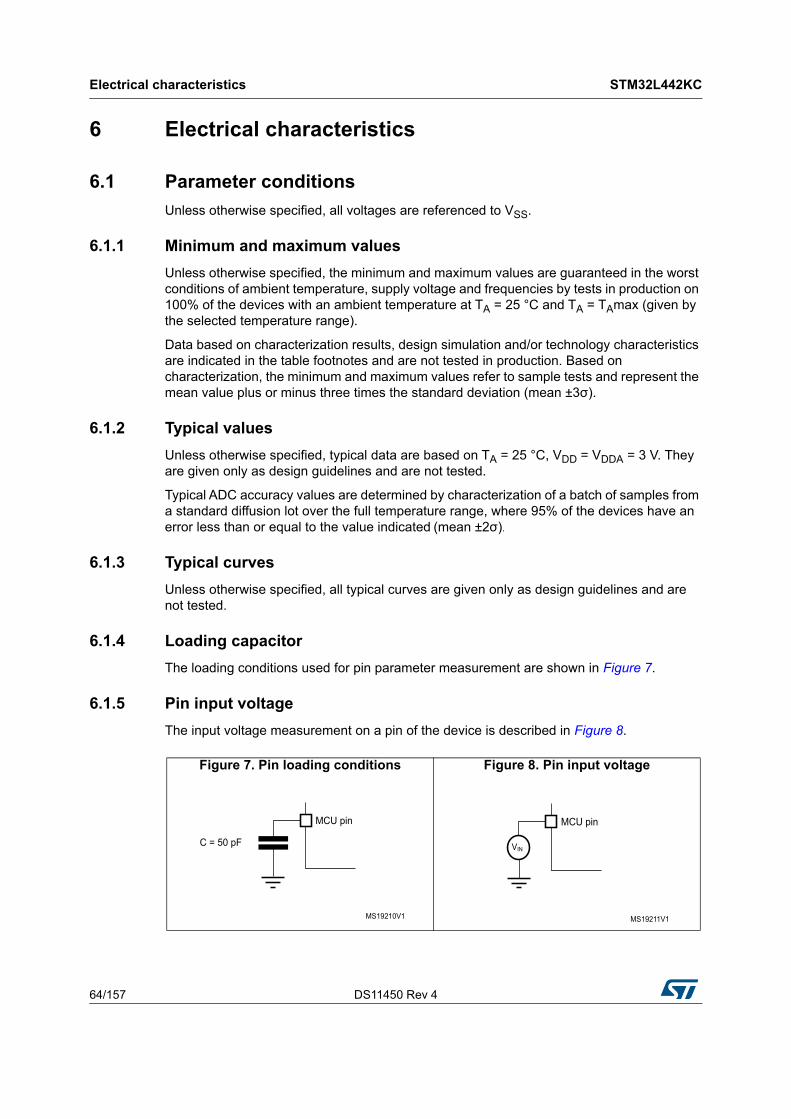
Electrical characteristics STM32L442KC
64/157 DS11450 Rev 4
6 Electrical characteristics
6.1 Parameter conditions
Unless otherwise specified, all voltages are referenced to VSS.
6.1.1 Minimum and maximum values
Unless otherwise specified, the minimum and maximum values are guaranteed in the worst conditions of ambient temperature, supply voltage and frequencies by tests in production on 100% of the devices with an ambient temperature at TA = 25 °C and TA = TAmax (given by the selected temperature range).
Data based on characterization results, design simulation and/or technology characteristics are indicated in the table footnotes and are not tested in production. Based on characterization, the minimum and maximum values refer to sample tests and represent the mean value plus or minus three times the standard deviation (mean ±3σ).
6.1.2 Typical values
Unless otherwise specified, typical data are based on TA = 25 °C, VDD = VDDA = 3 V. They are given only as design guidelines and are not tested.
Typical ADC accuracy values are determined by characterization of a batch of samples from a standard diffusion lot over the full temperature range, where 95% of the devices have an error less than or equal to the value indicated (mean ±2σ).
6.1.3 Typical curves
Unless otherwise specified, all typical curves are given only as design guidelines and are not tested.
6.1.4 Loading capacitor
The loading conditions used for pin parameter measurement are shown in Figure 7.
6.1.5 Pin input voltage
The input voltage measurement on a pin of the device is described in Figure 8.
Figure 7. Pin loading conditions Figure 8. Pin input voltage
MS19210V1
MCU pin
C = 50 pF
MS19211V1
MCU pin
VIN
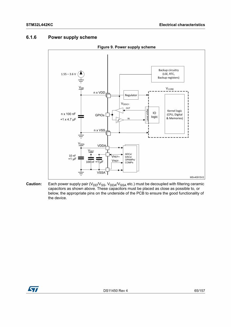
DS11450 Rev 4 65/157
STM32L442KC Electrical characteristics
149
6.1.6 Power supply scheme
Figure 9. Power supply scheme
Caution: Each power supply pair (VDD/VSS, VDDA/VSSA etc.) must be decoupled with filtering ceramic capacitors as shown above. These capacitors must be placed as close as possible to, or below, the appropriate pins on the underside of the PCB to ensure the good functionality of the device.
MSv40915V2
VDD
Leve
l shi
fter
IOlogic
Kernel logic(CPU, Digital& Memories)
Backup circuitry(LSE, RTC,
Backup registers)
IN
OUT
Regulator
GPIOs
1.55 – 3.6 V
n x 100 nF
+1 x 4.7 μF
n x VSS
n x VDDVCORE
VDDIO1
ADCs/DACs/OPAMPs/COMPs
VREF+
VREF-
VDDA
10 nF+1 μF
VDDA
VSSA
VREF
100 nF +1 μF
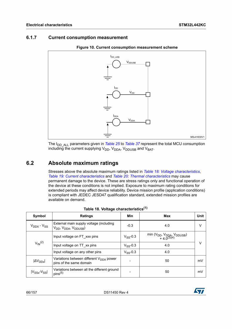
Electrical characteristics STM32L442KC
66/157 DS11450 Rev 4
6.1.7 Current consumption measurement
Figure 10. Current consumption measurement scheme
The IDD_ALL parameters given in Table 25 to Table 37 represent the total MCU consumption including the current supplying VDD, VDDA, VDDUSB and VBAT.
6.2 Absolute maximum ratings
Stresses above the absolute maximum ratings listed in Table 18: Voltage characteristics, Table 19: Current characteristics and Table 20: Thermal characteristics may cause permanent damage to the device. These are stress ratings only and functional operation of the device at these conditions is not implied. Exposure to maximum rating conditions for extended periods may affect device reliability. Device mission profile (application conditions) is compliant with JEDEC JESD47 qualification standard, extended mission profiles are available on demand.
MSv41630V1
IDD_USB
VDDUSB
IDD
VDD
IDDA
VDDA
Table 18. Voltage characteristics(1)
Symbol Ratings Min Max Unit
VDDX - VSSExternal main supply voltage (including VDD, VDDA, VDDUSB)
-0.3 4.0 V
VIN(2)
Input voltage on FT_xxx pins VSS-0.3min (VDD, VDDA, VDDUSB)
+ 4.0(3)(4)
VInput voltage on TT_xx pins VSS-0.3 4.0
Input voltage on any other pins VSS-0.3 4.0
|∆VDDx|Variations between different VDDX power pins of the same domain
- 50 mV
|VSSx-VSS|Variations between all the different ground pins(5) - 50 mV

DS11450 Rev 4 67/157
STM32L442KC Electrical characteristics
149
1. All main power (VDD, VDDA, VDDUSB) and ground (VSS, VSSA) pins must always be connected to the external power supply, in the permitted range.
2. VIN maximum must always be respected. Refer to Table 19: Current characteristics for the maximum allowed injected current values.
3. This formula has to be applied only on the power supplies related to the IO structure described in the pin definition table.
4. To sustain a voltage higher than 4 V the internal pull-up/pull-down resistors must be disabled.
5. Include VREF- pin.
Table 19. Current characteristics
Symbol Ratings Max Unit
∑IVDD Total current into sum of all VDD power lines (source)(1) 140
mA
∑IVSS Total current out of sum of all VSS ground lines (sink)(1) 140
IVDD(PIN) Maximum current into each VDD power pin (source)(1) 100
IVSS(PIN) Maximum current out of each VSS ground pin (sink)(1) 100
IIO(PIN)
Output current sunk by any I/O and control pin except FT_f 20
Output current sunk by any FT_f pin 20
Output current sourced by any I/O and control pin 20
∑IIO(PIN)
Total output current sunk by sum of all I/Os and control pins(2) 100
Total output current sourced by sum of all I/Os and control pins(2) 100
IINJ(PIN)(3)
Injected current on FT_xxx, TT_xx, RST and B pins, except PA4, PA5
-5/+0(4)
Injected current on PA4, PA5 -5/0
∑|IINJ(PIN)| Total injected current (sum of all I/Os and control pins)(5) 25
1. All main power (VDD, VDDA, VDDUSB) and ground (VSS, VSSA) pins must always be connected to the external power supplies, in the permitted range.
2. This current consumption must be correctly distributed over all I/Os and control pins. The total output current must not be sunk/sourced between two consecutive power supply pins referring to high pin count QFP packages.
3. Positive injection (when VIN > VDDIOx) is not possible on these I/Os and does not occur for input voltages lower than the specified maximum value.
4. A negative injection is induced by VIN < VSS. IINJ(PIN) must never be exceeded. Refer also to Table 18: Voltage characteristics for the maximum allowed input voltage values.
5. When several inputs are submitted to a current injection, the maximum ∑|IINJ(PIN)| is the absolute sum of the negative injected currents (instantaneous values).
Table 20. Thermal characteristics
Symbol Ratings Value Unit
TSTG Storage temperature range –65 to +150 °C
TJ Maximum junction temperature 150 °C
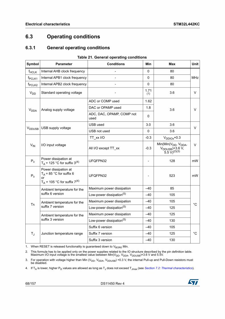
Electrical characteristics STM32L442KC
68/157 DS11450 Rev 4
6.3 Operating conditions
6.3.1 General operating conditions
Table 21. General operating conditions
Symbol Parameter Conditions Min Max Unit
fHCLK Internal AHB clock frequency - 0 80
MHzfPCLK1 Internal APB1 clock frequency - 0 80
fPCLK2 Internal APB2 clock frequency - 0 80
VDD Standard operating voltage -1.71
(1) 3.6 V
VDDA Analog supply voltage
ADC or COMP used 1.62
3.6 VDAC or OPAMP used 1.8
ADC, DAC, OPAMP, COMP not used
0
VDDUSB USB supply voltageUSB used 3.0 3.6
VUSB not used 0 3.6
VIN I/O input voltage
TT_xx I/O -0.3 VDDIOx+0.3
VAll I/O except TT_xx -0.3
Min(Min(VDD, VDDA, VDDUSB)+3.6 V,
5.5 V)(2)(3)
PDPower dissipation at TA = 125 °C for suffix 3(4) UFQFPN32 - 128 mW
PD
Power dissipation at TA = 85 °C for suffix 6 or TA = 105 °C for suffix 7(4)
UFQFPN32 - 523 mW
TA
Ambient temperature for the suffix 6 version
Maximum power dissipation –40 85
°C
Low-power dissipation(5) –40 105
Ambient temperature for the suffix 7 version
Maximum power dissipation –40 105
Low-power dissipation(5) –40 125
Ambient temperature for the suffix 3 version
Maximum power dissipation –40 125
Low-power dissipation(5) –40 130
TJ Junction temperature range
Suffix 6 version –40 105
°CSuffix 7 version –40 125
Suffix 3 version –40 130
1. When RESET is released functionality is guaranteed down to VBOR0 Min.
2. This formula has to be applied only on the power supplies related to the IO structure described by the pin definition table. Maximum I/O input voltage is the smallest value between Min(VDD, VDDA, VDDUSB)+3.6 V and 5.5V.
3. For operation with voltage higher than Min (VDD, VDDA, VDDUSB) +0.3 V, the internal Pull-up and Pull-Down resistors must be disabled.
4. If TA is lower, higher PD values are allowed as long as TJ does not exceed TJmax (see Section 7.2: Thermal characteristics).
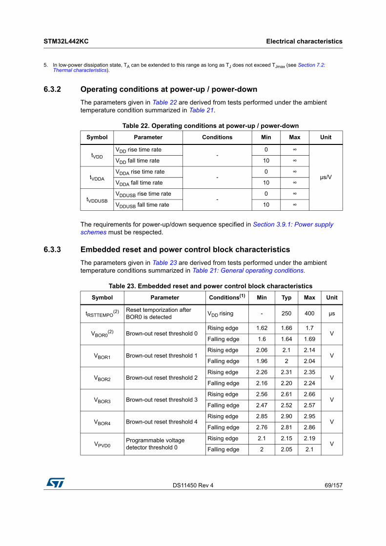
DS11450 Rev 4 69/157
STM32L442KC Electrical characteristics
149
6.3.2 Operating conditions at power-up / power-down
The parameters given in Table 22 are derived from tests performed under the ambient temperature condition summarized in Table 21.
The requirements for power-up/down sequence specified in Section 3.9.1: Power supply schemes must be respected.
6.3.3 Embedded reset and power control block characteristics
The parameters given in Table 23 are derived from tests performed under the ambient temperature conditions summarized in Table 21: General operating conditions.
5. In low-power dissipation state, TA can be extended to this range as long as TJ does not exceed TJmax (see Section 7.2: Thermal characteristics).
Table 22. Operating conditions at power-up / power-down
Symbol Parameter Conditions Min Max Unit
tVDD
VDD rise time rate-
0 ∞
µs/V
VDD fall time rate 10 ∞
tVDDA
VDDA rise time rate-
0 ∞
VDDA fall time rate 10 ∞
tVDDUSB
VDDUSB rise time rate-
0 ∞
VDDUSB fall time rate 10 ∞
Table 23. Embedded reset and power control block characteristics
Symbol Parameter Conditions(1) Min Typ Max Unit
tRSTTEMPO(2) Reset temporization after
BOR0 is detectedVDD rising - 250 400 μs
VBOR0(2) Brown-out reset threshold 0
Rising edge 1.62 1.66 1.7V
Falling edge 1.6 1.64 1.69
VBOR1 Brown-out reset threshold 1Rising edge 2.06 2.1 2.14
VFalling edge 1.96 2 2.04
VBOR2 Brown-out reset threshold 2Rising edge 2.26 2.31 2.35
VFalling edge 2.16 2.20 2.24
VBOR3 Brown-out reset threshold 3Rising edge 2.56 2.61 2.66
VFalling edge 2.47 2.52 2.57
VBOR4 Brown-out reset threshold 4Rising edge 2.85 2.90 2.95
VFalling edge 2.76 2.81 2.86
VPVD0Programmable voltage detector threshold 0
Rising edge 2.1 2.15 2.19V
Falling edge 2 2.05 2.1
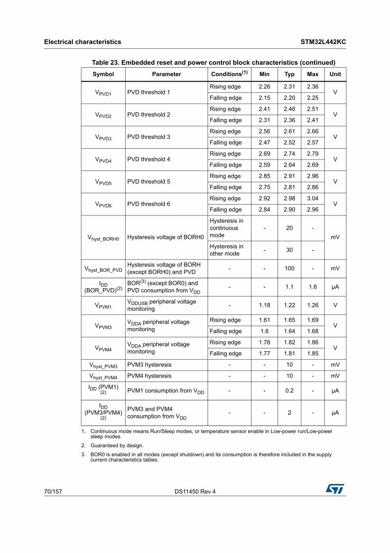
Electrical characteristics STM32L442KC
70/157 DS11450 Rev 4
VPVD1 PVD threshold 1Rising edge 2.26 2.31 2.36
VFalling edge 2.15 2.20 2.25
VPVD2 PVD threshold 2Rising edge 2.41 2.46 2.51
VFalling edge 2.31 2.36 2.41
VPVD3 PVD threshold 3Rising edge 2.56 2.61 2.66
VFalling edge 2.47 2.52 2.57
VPVD4 PVD threshold 4Rising edge 2.69 2.74 2.79
VFalling edge 2.59 2.64 2.69
VPVD5 PVD threshold 5Rising edge 2.85 2.91 2.96
VFalling edge 2.75 2.81 2.86
VPVD6 PVD threshold 6Rising edge 2.92 2.98 3.04
VFalling edge 2.84 2.90 2.96
Vhyst_BORH0 Hysteresis voltage of BORH0
Hysteresis in continuous mode
- 20 -
mV
Hysteresis in other mode
- 30 -
Vhyst_BOR_PVDHysteresis voltage of BORH (except BORH0) and PVD
- - 100 - mV
IDD (BOR_PVD)(2)
BOR(3) (except BOR0) and PVD consumption from VDD
- - 1.1 1.6 µA
VPVM1VDDUSB peripheral voltage monitoring
- 1.18 1.22 1.26 V
VPVM3VDDA peripheral voltage monitoring
Rising edge 1.61 1.65 1.69V
Falling edge 1.6 1.64 1.68
VPVM4VDDA peripheral voltage monitoring
Rising edge 1.78 1.82 1.86V
Falling edge 1.77 1.81 1.85
Vhyst_PVM3 PVM3 hysteresis - - 10 - mV
Vhyst_PVM4 PVM4 hysteresis - - 10 - mV
IDD (PVM1)(2) PVM1 consumption from VDD - - 0.2 - µA
IDD (PVM3/PVM4)
(2)
PVM3 and PVM4 consumption from VDD
- - 2 - µA
1. Continuous mode means Run/Sleep modes, or temperature sensor enable in Low-power run/Low-power sleep modes.
2. Guaranteed by design.
3. BOR0 is enabled in all modes (except shutdown) and its consumption is therefore included in the supply current characteristics tables.
Table 23. Embedded reset and power control block characteristics (continued)
Symbol Parameter Conditions(1) Min Typ Max Unit
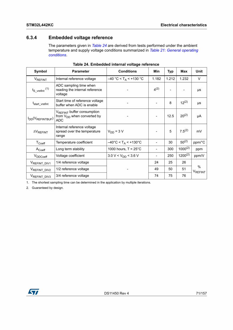
DS11450 Rev 4 71/157
STM32L442KC Electrical characteristics
149
6.3.4 Embedded voltage reference
The parameters given in Table 24 are derived from tests performed under the ambient temperature and supply voltage conditions summarized in Table 21: General operating conditions.
Table 24. Embedded internal voltage reference
Symbol Parameter Conditions Min Typ Max Unit
VREFINT Internal reference voltage –40 °C < TA < +130 °C 1.182 1.212 1.232 V
tS_vrefint (1)
ADC sampling time when reading the internal reference voltage
- 4(2) - - µs
tstart_vrefintStart time of reference voltage buffer when ADC is enable
- - 8 12(2) µs
IDD(VREFINTBUF)
VREFINT buffer consumption from VDD when converted by ADC
- - 12.5 20(2) µA
∆VREFINT
Internal reference voltage spread over the temperature range
VDD = 3 V - 5 7.5(2) mV
TCoeff Temperature coefficient –40°C < TA < +130°C - 30 50(2) ppm/°C
ACoeff Long term stability 1000 hours, T = 25°C - 300 1000(2) ppm
VDDCoeff Voltage coefficient 3.0 V < VDD < 3.6 V - 250 1200(2) ppm/V
VREFINT_DIV1 1/4 reference voltage
-
24 25 26%
VREFINTVREFINT_DIV2 1/2 reference voltage 49 50 51
VREFINT_DIV3 3/4 reference voltage 74 75 76
1. The shortest sampling time can be determined in the application by multiple iterations.
2. Guaranteed by design.
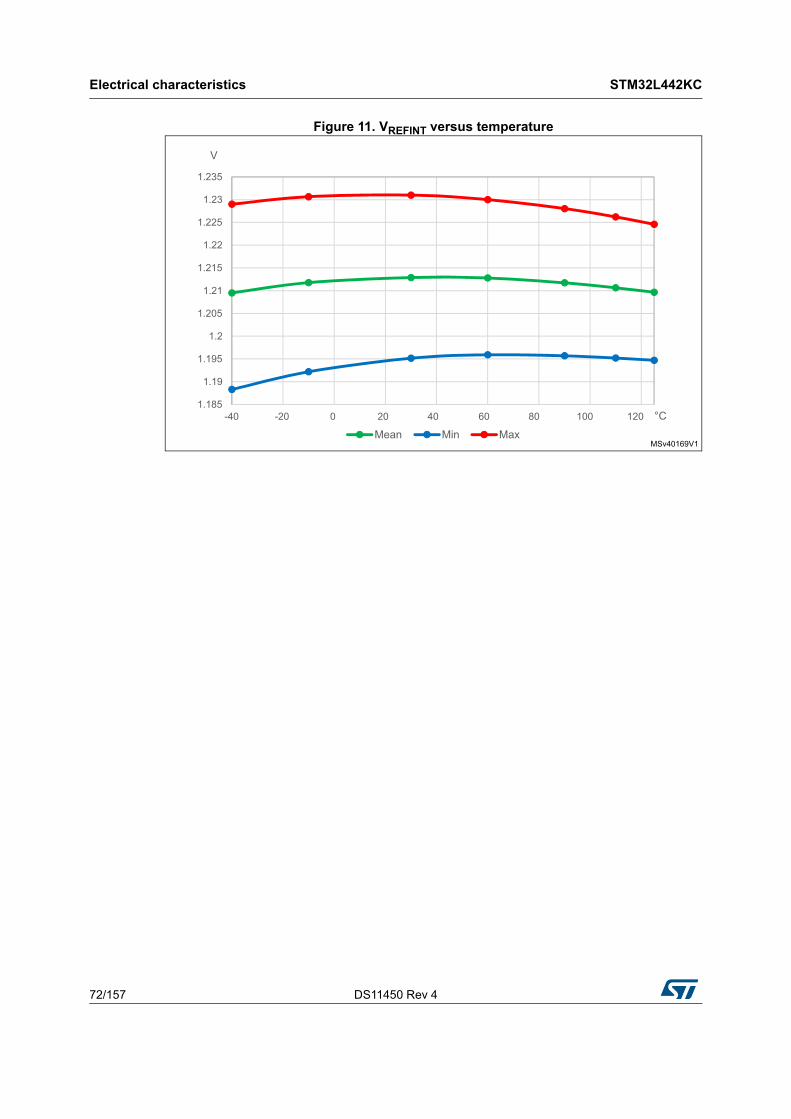
Electrical characteristics STM32L442KC
72/157 DS11450 Rev 4
Figure 11. VREFINT versus temperature
MSv40169V1
1.185
1.19
1.195
1.2
1.205
1.21
1.215
1.22
1.225
1.23
1.235
-40 -20 0 20 40 60 80 100 120
V
°C
Mean Min Max
DS11450 Rev 4 73/157
STM32L442KC Electrical characteristics
149
6.3.5 Supply current characteristics
The current consumption is a function of several parameters and factors such as the operating voltage, ambient temperature, I/O pin loading, device software configuration, operating frequencies, I/O pin switching rate, program location in memory and executed binary code.
The current consumption is measured as described in Figure 10: Current consumption measurement scheme.
Typical and maximum current consumption
The MCU is placed under the following conditions:
• All I/O pins are in analog input mode
• All peripherals are disabled except when explicitly mentioned
• The Flash memory access time is adjusted with the minimum wait states number, depending on the fHCLK frequency (refer to the table “Number of wait states according to CPU clock (HCLK) frequency” available in the RM0394 reference manual).
• When the peripherals are enabled fPCLK = fHCLK
The parameters given in Table 25 to Table 37 are derived from tests performed under ambient temperature and supply voltage conditions summarized in Table 21: General operating conditions.
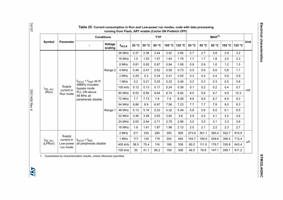
Elec
trical c
hara
cteristic
sS
TM
32
L4
42K
C
74/1
57D
S114
50 Rev 4
Table 25. Current consumption in Run and Low-power run modes, code with data processing running from Flash, ART enable (Cache ON Prefetch OFF)
Symbol Parameter
Conditions TYP MAX(1)
Unit- Voltage
scalingfHCLK 25 °C 55 °C 85 °C 105 °C 125 °C 25 °C 55 °C 85 °C 105 °C 125 °C
IDD_ALL(Run)
Supply current in Run mode
fHCLK = fHSE up to 48MHz included, bypass mode PLL ON above 48 MHz all peripherals disable
Range 2
26 MHz 2.37 2.38 2.44 2.52 2.66 2.7 2.7 2.8 2.9 3.2
mA
16 MHz 1.5 1.52 1.57 1.64 1.79 1.7 1.7 1.8 2.0 2.3
8 MHz 0.81 0.82 0.87 0.94 1.08 0.9 0.9 1.0 1.2 1.5
4 MHz 0.46 0.47 0.52 0.59 0.73 0.5 0.6 0.6 0.8 1.1
2 MHz 0.29 0.3 0.34 0.41 0.55 0.3 0.4 0.4 0.6 0.9
1 MHz 0.2 0.21 0.25 0.32 0.46 0.2 0.3 0.3 0.5 0.8
100 kHz 0.12 0.13 0.17 0.24 0.38 0.1 0.2 0.2 0.4 0.7
Range 1
80 MHz 8.53 8.56 8.64 8.74 8.92 9.5 9.6 9.7 9.9 10.3
72 MHz 7.7 7.73 7.8 7.9 8.08 8.6 8.6 8.7 8.9 9.3
64 MHz 6.86 6.9 6.97 7.06 7.23 7.7 7.7 7.8 8.0 8.3
48 MHz 5.13 5.16 5.23 5.32 5.49 5.8 5.8 6.0 6.1 6.5
32 MHz 3.46 3.48 3.55 3.64 3.8 3.9 4.0 4.1 4.2 4.6
24 MHz 2.63 2.64 2.71 2.79 2.96 3.0 3.0 3.1 3.3 3.6
16 MHz 1.8 1.81 1.87 1.96 2.12 2.0 2.1 2.2 2.3 2.7
IDD_ALL(LPRun)
Supply current in
Low-power run mode
fHCLK = fMSI all peripherals disable
2 MHz 211 230 280 355 506 273.8 301.1 360.4 502.7 815.9
µA1 MHz 117 134 179 254 404 154.7 184.6 249.6 398.4 712.4
400 kHz 58.5 70.4 116 189 338 80.2 111.5 179.7 330.8 643.4
100 kHz 30 41.1 85.2 159 308 46.5 76.6 147.1 299.1 611.2
1. Guaranteed by characterization results, unless otherwise specified.
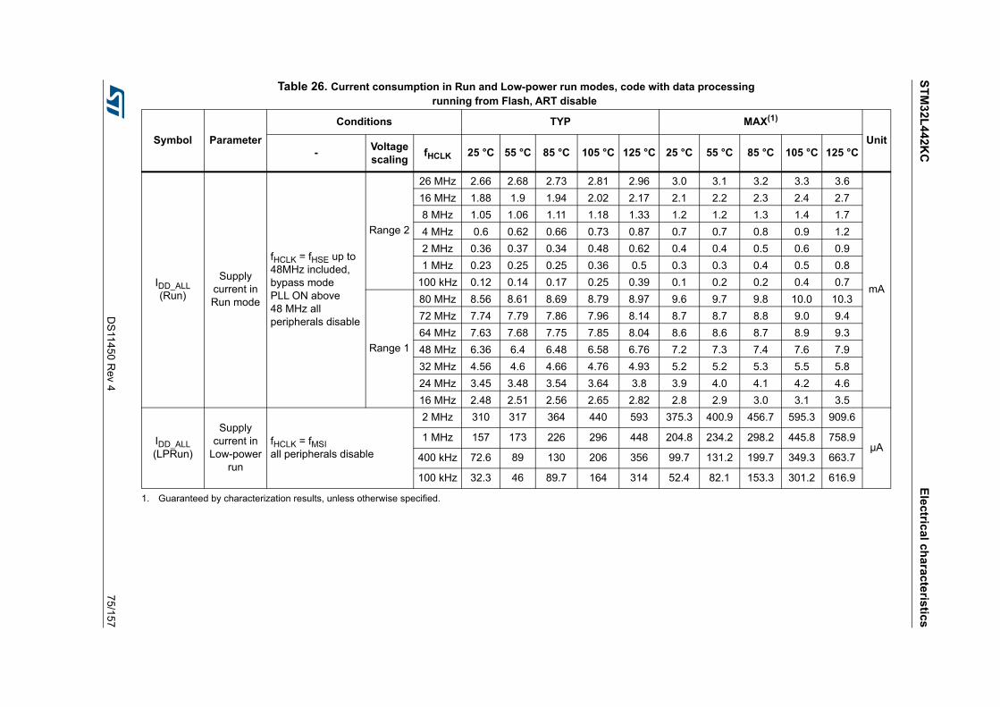
ST
M3
2L4
42K
CE
lectric
al cha
racte
ristic
s
DS
11450 R
ev 475/157
Table 26. Current consumption in Run and Low-power run modes, code with data processingrunning from Flash, ART disable
Symbol Parameter
Conditions TYP MAX(1)
Unit-
Voltage scaling
fHCLK 25 °C 55 °C 85 °C 105 °C 125 °C 25 °C 55 °C 85 °C 105 °C 125 °C
IDD_ALL(Run)
Supply current in Run mode
fHCLK = fHSE up to 48MHz included, bypass mode PLL ON above 48 MHz all peripherals disable
Range 2
26 MHz 2.66 2.68 2.73 2.81 2.96 3.0 3.1 3.2 3.3 3.6
mA
16 MHz 1.88 1.9 1.94 2.02 2.17 2.1 2.2 2.3 2.4 2.7
8 MHz 1.05 1.06 1.11 1.18 1.33 1.2 1.2 1.3 1.4 1.7
4 MHz 0.6 0.62 0.66 0.73 0.87 0.7 0.7 0.8 0.9 1.2
2 MHz 0.36 0.37 0.34 0.48 0.62 0.4 0.4 0.5 0.6 0.9
1 MHz 0.23 0.25 0.25 0.36 0.5 0.3 0.3 0.4 0.5 0.8
100 kHz 0.12 0.14 0.17 0.25 0.39 0.1 0.2 0.2 0.4 0.7
Range 1
80 MHz 8.56 8.61 8.69 8.79 8.97 9.6 9.7 9.8 10.0 10.3
72 MHz 7.74 7.79 7.86 7.96 8.14 8.7 8.7 8.8 9.0 9.4
64 MHz 7.63 7.68 7.75 7.85 8.04 8.6 8.6 8.7 8.9 9.3
48 MHz 6.36 6.4 6.48 6.58 6.76 7.2 7.3 7.4 7.6 7.9
32 MHz 4.56 4.6 4.66 4.76 4.93 5.2 5.2 5.3 5.5 5.8
24 MHz 3.45 3.48 3.54 3.64 3.8 3.9 4.0 4.1 4.2 4.6
16 MHz 2.48 2.51 2.56 2.65 2.82 2.8 2.9 3.0 3.1 3.5
IDD_ALL(LPRun)
Supply current in
Low-power run
fHCLK = fMSI all peripherals disable
2 MHz 310 317 364 440 593 375.3 400.9 456.7 595.3 909.6
µA1 MHz 157 173 226 296 448 204.8 234.2 298.2 445.8 758.9
400 kHz 72.6 89 130 206 356 99.7 131.2 199.7 349.3 663.7
100 kHz 32.3 46 89.7 164 314 52.4 82.1 153.3 301.2 616.9
1. Guaranteed by characterization results, unless otherwise specified.
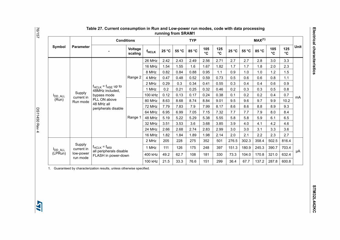
Elec
trical c
hara
cteristic
sS
TM
32
L4
42K
C
76/1
57D
S114
50 Rev 4
Table 27. Current consumption in Run and Low-power run modes, code with data processing running from SRAM1
Symbol Parameter
Conditions TYP MAX(1)
Unit-
Voltage scaling
fHCLK 25 °C 55 °C 85 °C105 °C
125 °C
25 °C 55 °C 85 °C105 °C
125 °C
IDD_ALL(Run)
Supply current in Run mode
fHCLK = fHSE up to 48MHz included, bypass mode PLL ON above 48 MHz all peripherals disable
Range 2
26 MHz 2.42 2.43 2.49 2.56 2.71 2.7 2.7 2.8 3.0 3.3
mA
16 MHz 1.54 1.55 1.6 1.67 1.82 1.7 1.7 1.8 2.0 2.3
8 MHz 0.82 0.84 0.88 0.95 1.1 0.9 1.0 1.0 1.2 1.5
4 MHz 0.47 0.48 0.52 0.59 0.73 0.5 0.6 0.6 0.8 1.1
2 MHz 0.29 0.3 0.34 0.41 0.55 0.3 0.4 0.4 0.6 0.9
1 MHz 0.2 0.21 0.25 0.32 0.46 0.2 0.3 0.3 0.5 0.8
100 kHz 0.12 0.13 0.17 0.24 0.38 0.1 0.2 0.2 0.4 0.7
Range 1
80 MHz 8.63 8.68 8.74 8.84 9.01 9.5 9.6 9.7 9.9 10.2
72 MHz 7.79 7.83 7.9 7.99 8.17 8.6 8.6 8.8 8.9 9.3
64 MHz 6.95 6.99 7.05 7.15 7.32 7.7 7.7 7.9 8.0 8.4
48 MHz 5.19 5.22 5.29 5.38 5.55 5.8 5.8 5.9 6.1 6.5
32 MHz 3.51 3.53 3.6 3.68 3.85 3.9 4.0 4.1 4.2 4.6
24 MHz 2.66 2.68 2.74 2.83 2.99 3.0 3.0 3.1 3.3 3.6
16 MHz 1.82 1.84 1.89 1.98 2.14 2.0 2.1 2.2 2.3 2.7
IDD_ALL(LPRun)
Supply current in low-power run mode
fHCLK = fMSI all peripherals disable FLASH in power-down
2 MHz 205 228 275 352 501 276.5 302.3 358.4 502.5 816.4
µA1 MHz 111 126 175 248 397 151.3 180.9 245.3 390.7 703.4
400 kHz 49.2 62.7 108 181 330 73.3 104.0 170.8 321.0 632.4
100 kHz 21.5 33.3 76.6 151 299 36.4 67.7 137.2 287.8 600.8
1. Guaranteed by characterization results, unless otherwise specified.
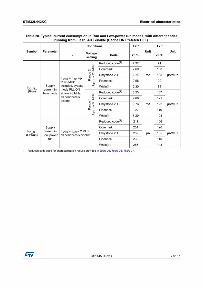
DS11450 Rev 4 77/157
STM32L442KC Electrical characteristics
149
Table 28. Typical current consumption in Run and Low-power run modes, with different codesrunning from Flash, ART enable (Cache ON Prefetch OFF)
Symbol Parameter
Conditions TYP
Unit
TYP
Unit-
Voltage scaling
Code 25 °C 25 °C
IDD_ALL(Run)
Supply current in Run mode
fHCLK = fHSE up to 48 MHz included, bypass mode PLL ON above 48 MHz all peripherals disable
Ra
nge
2f H
CLK
= 2
6 M
Hz Reduced code(1) 2.37
mA
91
µA/MHz
Coremark 2.69 103
Dhrystone 2.1 2.74 105
Fibonacci 2.58 99
While(1) 2.30 88R
ange
1f H
CL
K =
80
MH
z Reduced code(1) 8.53
mA
107
µA/MHz
Coremark 9.68 121
Dhrystone 2.1 9.76 122
Fibonacci 9.27 116
While(1) 8.20 103
IDD_ALL(LPRun)
Supply current in
Low-power run
fHCLK = fMSI = 2 MHz all peripherals disable
Reduced code(1) 211
µA
106
µA/MHz
Coremark 251 126
Dhrystone 2.1 269 135
Fibonacci 230 115
While(1) 286 143
1. Reduced code used for characterization results provided in Table 25, Table 26, Table 27.
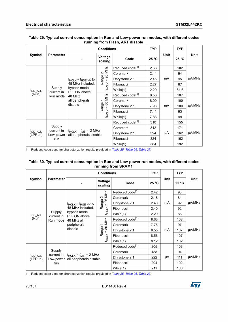
Electrical characteristics STM32L442KC
78/157 DS11450 Rev 4
Table 29. Typical current consumption in Run and Low-power run modes, with different codesrunning from Flash, ART disable
Symbol Parameter
Conditions TYP
Unit
TYP
Unit-
Voltage scaling
Code 25 °C 25 °C
IDD_ALL(Run)
Supply current in Run mode
fHCLK = fHSE up to 48 MHz included, bypass mode PLL ON above 48 MHz all peripherals disable
Ran
ge
2f H
CL
K =
26
MH
z Reduced code(1) 2.66
mA
102
µA/MHz
Coremark 2.44 94
Dhrystone 2.1 2.46 95
Fibonacci 2.27 87
While(1) 2.20 84.6
Ran
ge 1
f HC
LK =
80
MH
z Reduced code(1) 8.56
mA
107
µA/MHz
Coremark 8.00 100
Dhrystone 2.1 7.98 100
Fibonacci 7.41 93
While(1) 7.83 98
IDD_ALL(LPRun)
Supply current in
Low-power run
fHCLK = fMSI = 2 MHz all peripherals disable
Reduced code(1) 310
µA
155
µA/MHz
Coremark 342 171
Dhrystone 2.1 324 162
Fibonacci 324 162
While(1) 384 192
1. Reduced code used for characterization results provided in Table 25, Table 26, Table 27.
Table 30. Typical current consumption in Run and Low-power run modes, with different codesrunning from SRAM1
Symbol Parameter
Conditions TYP
Unit
TYP
Unit-
Voltage scaling
Code 25 °C 25 °C
IDD_ALL(Run)
Supply current in Run mode
fHCLK = fHSE up to 48 MHz included, bypass mode PLL ON above 48 MHz all peripherals disable
Ran
ge 2
f HC
LK =
26
MH
z Reduced code(1) 2.42
mA
93
µA/MHz
Coremark 2.18 84
Dhrystone 2.1 2.40 92
Fibonacci 2.40 92
While(1) 2.29 88
Ran
ge
1f H
CL
K =
80
MH
z Reduced code(1) 8.63
mA
108
µA/MHz
Coremark 7.76 97
Dhrystone 2.1 8.55 107
Fibonacci 8.56 107
While(1) 8.12 102
IDD_ALL(LPRun)
Supply current in
Low-power run
fHCLK = fMSI = 2 MHz all peripherals disable
Reduced code(1) 205
µA
103
µA/MHz
Coremark 188 94
Dhrystone 2.1 222 111
Fibonacci 204 102
While(1) 211 106
1. Reduced code used for characterization results provided in Table 25, Table 26, Table 27.
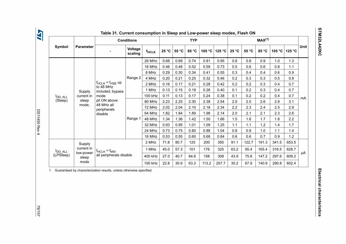
ST
M3
2L4
42K
CE
lectric
al cha
racte
ristic
s
DS
11450 R
ev 479/157
Table 31. Current consumption in Sleep and Low-power sleep modes, Flash ON
Symbol Parameter
Conditions TYP MAX(1)
Unit-
Voltage scaling
fHCLK 25 °C 55 °C 85 °C 105 °C 125 °C 25 °C 55 °C 85 °C 105 °C 125 °C
IDD_ALL(Sleep)
Supply current in
sleep mode,
fHCLK = fHSE up to 48 MHz included, bypass mode pll ON above 48 MHz all peripherals disable
Range 2
26 MHz 0.68 0.69 0.74 0.81 0.95 0.8 0.8 0.9 1.0 1.3
mA
16 MHz 0.46 0.48 0.52 0.59 0.73 0.5 0.6 0.6 0.8 1.1
8 MHz 0.29 0.30 0.34 0.41 0.55 0.3 0.4 0.4 0.6 0.9
4 MHz 0.20 0.21 0.25 0.32 0.46 0.2 0.3 0.3 0.5 0.8
2 MHz 0.16 0.17 0.21 0.28 0.42 0.2 0.2 0.3 0.4 0.7
1 MHz 0.13 0.15 0.19 0.26 0.40 0.1 0.2 0.3 0.4 0.7
100 kHz 0.11 0.13 0.17 0.24 0.38 0.1 0.2 0.2 0.4 0.7
Range 1
80 MHz 2.23 2.25 2.30 2.38 2.54 2.5 2.5 2.6 2.8 3.1
72 MHz 2.02 2.04 2.10 2.18 2.34 2.2 2.3 2.4 2.5 2.9
64 MHz 1.82 1.84 1.89 1.98 2.14 2.0 2.1 2.1 2.3 2.6
48 MHz 1.34 1.36 1.42 1.50 1.66 1.5 1.6 1.7 1.8 2.2
32 MHz 0.93 0.95 1.01 1.09 1.25 1.1 1.1 1.2 1.4 1.7
24 MHz 0.73 0.75 0.80 0.88 1.04 0.8 0.9 1.0 1.1 1.4
16 MHz 0.53 0.55 0.60 0.68 0.84 0.6 0.6 0.7 0.9 1.2
IDD_ALL(LPSleep)
Supply current in low-power
sleep mode
fHCLK = fMSI all peripherals disable
2 MHz 71.8 80.7 125 200 350 91.1 122.7 191.3 341.5 653.5
µA1 MHz 45.0 57.3 101 176 325 63.2 95.4 165.4 316.5 628.7
400 kHz 27.0 40.7 84.6 158 308 43.9 75.8 147.2 297.6 609.2
100 kHz 22.8 30.9 63.3 113.2 207.7 35.2 67.9 140.9 290.8 602.4
1. Guaranteed by characterization results, unless otherwise specified.
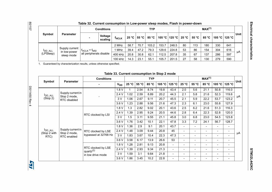
Elec
trical c
hara
cteristic
sS
TM
32
L4
42K
C
80/1
57D
S114
50 Rev 4
Table 32. Current consumption in Low-power sleep modes, Flash in power-down
Symbol Parameter
Conditions TYP MAX(1)
Unit-
Voltage scaling
fHCLK 25 °C 55 °C 85 °C 105 °C 125 °C 25 °C 55 °C 85 °C 105 °C 125 °C
IDD_ALL(LPSleep)
Supply current in low-power sleep mode
fHCLK = fMSI all peripherals disable
2 MHz 58.7 70.7 103.2 153.7 248.5 80 113 180 330 641
µA1 MHz 39.4 47.2 79.3 129.6 224.8 53 86 154 304 616
400 kHz 20.8 30.8 62.1 112.5 207.8 35 67 137 286 597
100 kHz 14.3 23.1 55.1 105.7 201.5 27 58 130 279 590
1. Guaranteed by characterization results, unless otherwise specified.
Table 33. Current consumption in Stop 2 mode
Symbol ParameterConditions TYP MAX(1)
Unit- VDD 25 °C 55 °C 85 °C 105 °C 125 °C 25 °C 55 °C 85 °C 105 °C 125 °C
IDD_ALL(Stop 2)
Supply current in Stop 2 mode, RTC disabled
-
1.8 V 1 2.54 8.74 19.8 43.4 2.0 5.6 21.1 50.8 116.0
µA2.4 V 1.02 2.59 8.89 20.2 44.3 2.1 5.8 21.6 52.3 119.6
3 V 1.06 2.67 9.11 20.7 45.5 2.1 5.9 22.2 53.7 123.2
3.6 V 1.23 2.88 9.56 21.6 47.3 2.3 6.1 23.0 55.8 127.9
IDD_ALL(Stop 2 with
RTC)
Supply current in Stop 2 mode, RTC enabled
RTC clocked by LSI
1.8 V 1.3 2.82 9.02 20.1 43.6 2.5 6.2 21.6 51.3 116.3
µA
2.4 V 1.39 2.95 9.24 20.5 44.6 2.8 6.4 22.3 52.8 120.0
3 V 1.5 3.11 9.55 21.1 45.8 3.0 6.8 23.0 54.5 123.8
3.6 V 1.76 3.42 10.1 22.1 47.8 3.3 7.2 24.1 56.7 128.7
RTC clocked by LSE bypassed at 32768 Hz
1.8 V 1.36 2.9 9.1 20.1 43.7 - - - - -
2.4 V 1.48 3.09 9.44 20.8 45 - - - - -
3 V 1.83 3.67 10.4 22.3 47.3 - - - - -
3.6 V 3.58 6.17 13.9 26.6 53 - - - - -
RTC clocked by LSE quartz(2) in low drive mode
1.8 V 1.28 2.81 9.13 20.8 - - - - - -
2.4 V 1.39 2.93 9.34 21.3 - - - - - -
3 V 1.59 3.1 9.64 21.8 - - - - - -
3.6 V 1.86 3.45 10.2 22.8 - - - - - -
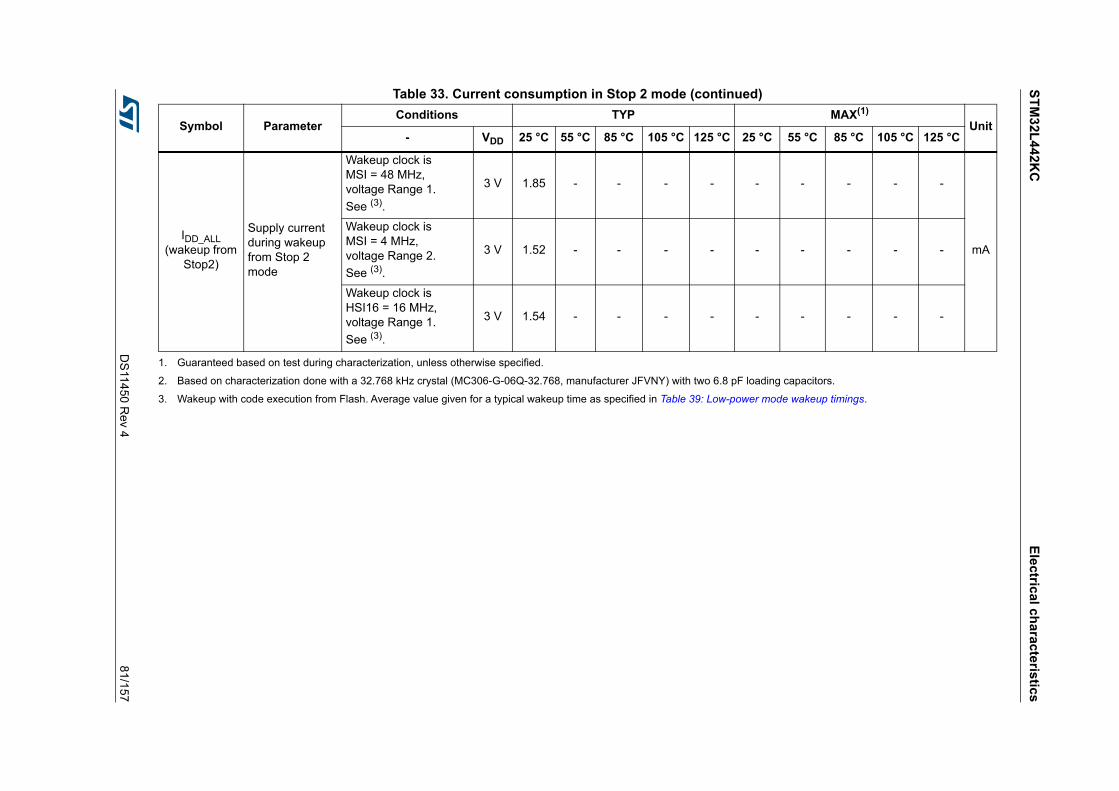
ST
M3
2L4
42K
CE
lectric
al cha
racte
ristic
s
DS
11450 R
ev 481/157
IDD_ALL(wakeup from
Stop2)
Supply current during wakeup from Stop 2 mode
Wakeup clock is MSI = 48 MHz, voltage Range 1.
See (3).
3 V 1.85 - - - - - - - - -
mA
Wakeup clock is MSI = 4 MHz, voltage Range 2.
See (3).
3 V 1.52 - - - - - - - - -
Wakeup clock is HSI16 = 16 MHz, voltage Range 1.
See (3).
3 V 1.54 - - - - - - - - -
1. Guaranteed based on test during characterization, unless otherwise specified.
2. Based on characterization done with a 32.768 kHz crystal (MC306-G-06Q-32.768, manufacturer JFVNY) with two 6.8 pF loading capacitors.
3. Wakeup with code execution from Flash. Average value given for a typical wakeup time as specified in Table 39: Low-power mode wakeup timings.
Table 33. Current consumption in Stop 2 mode (continued)
Symbol ParameterConditions TYP MAX(1)
Unit- VDD 25 °C 55 °C 85 °C 105 °C 125 °C 25 °C 55 °C 85 °C 105 °C 125 °C
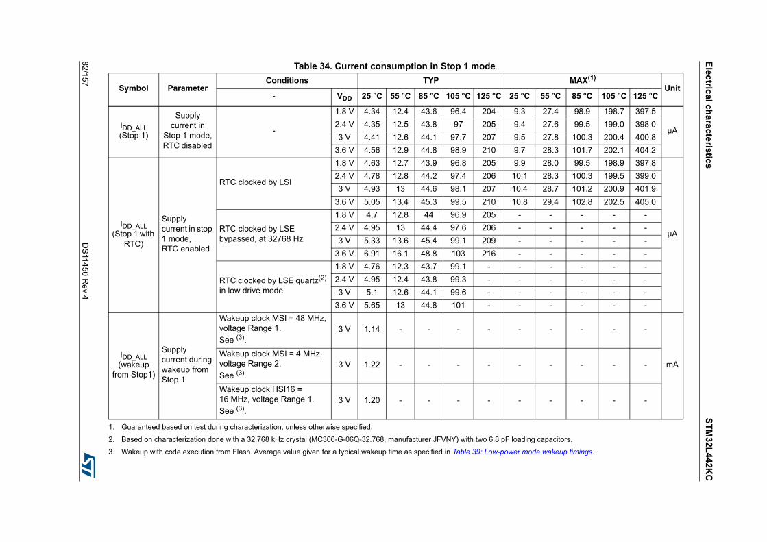
Elec
trical c
hara
cteristic
sS
TM
32
L4
42K
C
82/1
57D
S114
50 Rev 4
Table 34. Current consumption in Stop 1 mode
Symbol ParameterConditions TYP MAX(1)
Unit- VDD 25 °C 55 °C 85 °C 105 °C 125 °C 25 °C 55 °C 85 °C 105 °C 125 °C
IDD_ALL(Stop 1)
Supply current in
Stop 1 mode,RTC disabled
-
1.8 V 4.34 12.4 43.6 96.4 204 9.3 27.4 98.9 198.7 397.5
µA2.4 V 4.35 12.5 43.8 97 205 9.4 27.6 99.5 199.0 398.0
3 V 4.41 12.6 44.1 97.7 207 9.5 27.8 100.3 200.4 400.8
3.6 V 4.56 12.9 44.8 98.9 210 9.7 28.3 101.7 202.1 404.2
IDD_ALL(Stop 1 with
RTC)
Supply current in stop 1 mode, RTC enabled
RTC clocked by LSI
1.8 V 4.63 12.7 43.9 96.8 205 9.9 28.0 99.5 198.9 397.8
µA
2.4 V 4.78 12.8 44.2 97.4 206 10.1 28.3 100.3 199.5 399.0
3 V 4.93 13 44.6 98.1 207 10.4 28.7 101.2 200.9 401.9
3.6 V 5.05 13.4 45.3 99.5 210 10.8 29.4 102.8 202.5 405.0
RTC clocked by LSE bypassed, at 32768 Hz
1.8 V 4.7 12.8 44 96.9 205 - - - - -
2.4 V 4.95 13 44.4 97.6 206 - - - - -
3 V 5.33 13.6 45.4 99.1 209 - - - - -
3.6 V 6.91 16.1 48.8 103 216 - - - - -
RTC clocked by LSE quartz(2) in low drive mode
1.8 V 4.76 12.3 43.7 99.1 - - - - - -
2.4 V 4.95 12.4 43.8 99.3 - - - - - -
3 V 5.1 12.6 44.1 99.6 - - - - - -
3.6 V 5.65 13 44.8 101 - - - - - -
IDD_ALL(wakeup
from Stop1)
Supply current during wakeup from Stop 1
Wakeup clock MSI = 48 MHz, voltage Range 1.
See (3).3 V 1.14 - - - - - - - - -
mAWakeup clock MSI = 4 MHz, voltage Range 2.
See (3).3 V 1.22 - - - - - - - - -
Wakeup clock HSI16 = 16 MHz, voltage Range 1.
See (3).3 V 1.20 - - - - - - - - -
1. Guaranteed based on test during characterization, unless otherwise specified.
2. Based on characterization done with a 32.768 kHz crystal (MC306-G-06Q-32.768, manufacturer JFVNY) with two 6.8 pF loading capacitors.
3. Wakeup with code execution from Flash. Average value given for a typical wakeup time as specified in Table 39: Low-power mode wakeup timings.
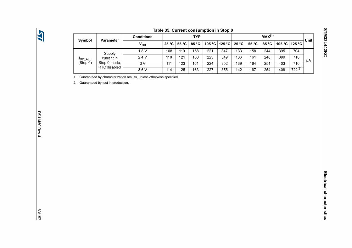
ST
M3
2L4
42K
CE
lectric
al cha
racte
ristic
s
DS
11450 R
ev 483/157
Table 35. Current consumption in Stop 0
Symbol ParameterConditions TYP MAX(1)
1. Guaranteed by characterization results, unless otherwise specified.
UnitVDD 25 °C 55 °C 85 °C 105 °C 125 °C 25 °C 55 °C 85 °C 105 °C 125 °C
IDD_ALL(Stop 0)
Supply current in
Stop 0 mode,RTC disabled
1.8 V 108 119 158 221 347 133 158 244 395 704
µA2.4 V 110 121 160 223 349 136 161 248 399 710
3 V 111 123 161 224 352 139 164 251 403 716
3.6 V 114 125 163 227 355 142 167 254 408 722(2)
2. Guaranteed by test in production.

Elec
trical c
hara
cteristic
sS
TM
32
L4
42K
C
84/1
57D
S114
50 Rev 4
Table 36. Current consumption in Standby mode
Symbol ParameterConditions TYP MAX(1)
Unit- VDD 25 °C 55 °C 85 °C 105 °C 125 °C 25 °C 55 °C 85 °C 105 °C 125 °C
IDD_ALL(Standby)
Supply current in Standby mode (backup registers retained), RTC disabled
no independent watchdog
1.8 V 27.7 144 758 2 072 5 425 119 425 2866 7524 20510
nA
2.4 V 50.9 187 892 2 408 6 247 183 564 3383 8778 23768
3 V 90.2 253 1 090 2 884 7 409 225 681 3912 10071 26976
3.6 V 253 459 1 474 3 575 8 836 292 877 4638 11659 30758
with independent watchdog
1.8 V 216 - - - - - - - - -
2.4 V 342 - - - - - - - - -
3 V 416 - - - - - - - - -
3.6 V 551 - - - - - - - - -
IDD_ALL(Standby with RTC)
Supply current in Standby mode (backup registers retained), RTC enabled
RTC clocked by LSI, no independent watchdog
1.8 V 287 407 989 2 230 5 396 585 944 3344 7866 20504
nA
2.4 V 386 526 1 201 2 638 6 274 811 1230 4007 9246 23824
3 V 513 679 1 478 3 167 7 414 1022 1521 4683 10671 27124
3.6 V 771 978 1 963 3 992 9 039 1284 1924 5577 1238330954
(2)
RTC clocked by LSI, with independent watchdog
1.8 V 342 - - - - - - - - -
2.4 V 521 - - - - - - - - -
3 V 655 - - - - - - - - -
3.6 V 865 - - - - - - - - -
RTC clocked by LSE bypassed at 32768Hz
1.8 V 142 126 865 2 220 5 650 - - - - -
nA
2.4 V 249 219 1 090 2 660 6 600 - - - - -
3 V 404 364 1 410 3 260 7 850 - - - - -
3.6 V 742 670 2 000 4 230 9 700 - - - - -
RTC clocked by LSE quartz (3) in low drive mode
1.8 V 281 423 1 046 2 410 5 700 - - - - -
2.4 V 388 548 1 268 2 847 6 564 - - - - -
3 V 535 715 1 565 3 420 7 694 - - - - -
3.6 V 836 1 048 2 081 4 311 9 338 - - - - -
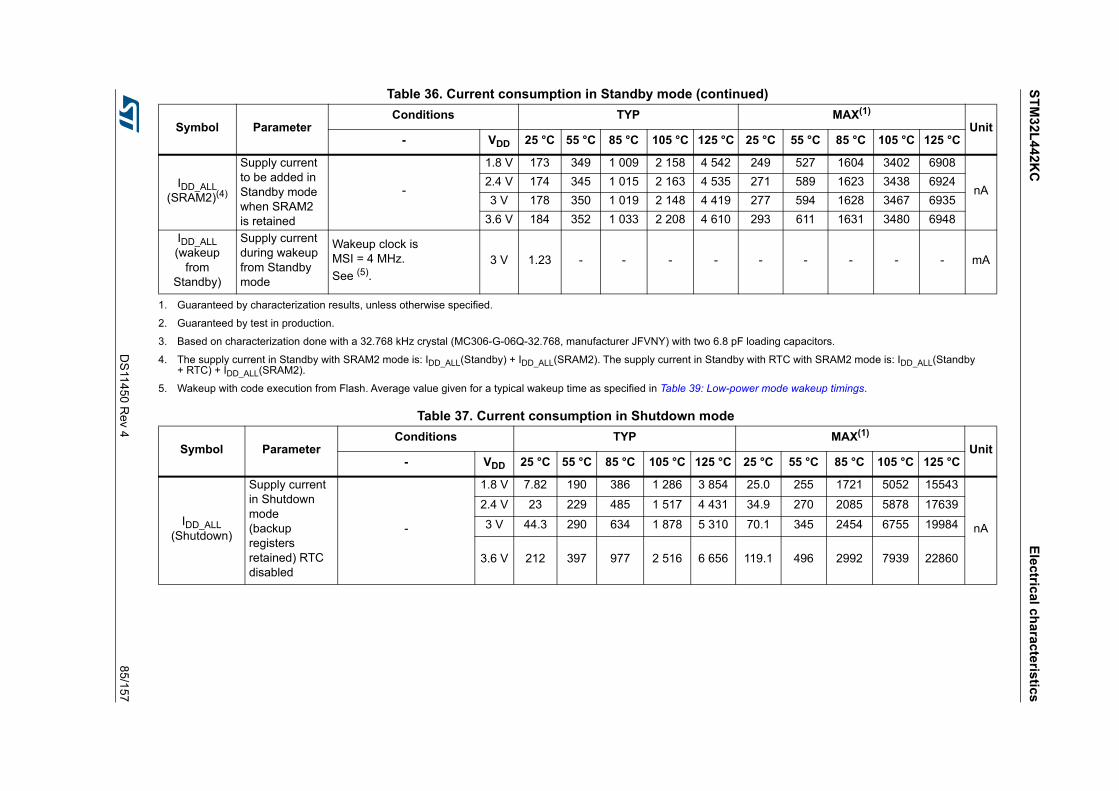
ST
M3
2L4
42K
CE
lectric
al cha
racte
ristic
s
DS
11450 R
ev 485/157
IDD_ALL(SRAM2)(4)
Supply current to be added in Standby mode when SRAM2 is retained
-
1.8 V 173 349 1 009 2 158 4 542 249 527 1604 3402 6908
nA2.4 V 174 345 1 015 2 163 4 535 271 589 1623 3438 6924
3 V 178 350 1 019 2 148 4 419 277 594 1628 3467 6935
3.6 V 184 352 1 033 2 208 4 610 293 611 1631 3480 6948
IDD_ALL(wakeup
from Standby)
Supply current during wakeup from Standby mode
Wakeup clock is MSI = 4 MHz.
See (5).3 V 1.23 - - - - - - - - - mA
1. Guaranteed by characterization results, unless otherwise specified.
2. Guaranteed by test in production.
3. Based on characterization done with a 32.768 kHz crystal (MC306-G-06Q-32.768, manufacturer JFVNY) with two 6.8 pF loading capacitors.
4. The supply current in Standby with SRAM2 mode is: IDD_ALL(Standby) + IDD_ALL(SRAM2). The supply current in Standby with RTC with SRAM2 mode is: IDD_ALL(Standby + RTC) + IDD_ALL(SRAM2).
5. Wakeup with code execution from Flash. Average value given for a typical wakeup time as specified in Table 39: Low-power mode wakeup timings.
Table 36. Current consumption in Standby mode (continued)
Symbol ParameterConditions TYP MAX(1)
Unit- VDD 25 °C 55 °C 85 °C 105 °C 125 °C 25 °C 55 °C 85 °C 105 °C 125 °C
Table 37. Current consumption in Shutdown mode
Symbol ParameterConditions TYP MAX(1)
Unit- VDD 25 °C 55 °C 85 °C 105 °C 125 °C 25 °C 55 °C 85 °C 105 °C 125 °C
IDD_ALL(Shutdown)
Supply current in Shutdown mode (backup registers retained) RTC disabled
-
1.8 V 7.82 190 386 1 286 3 854 25.0 255 1721 5052 15543
nA
2.4 V 23 229 485 1 517 4 431 34.9 270 2085 5878 17639
3 V 44.3 290 634 1 878 5 310 70.1 345 2454 6755 19984
3.6 V 212 397 977 2 516 6 656 119.1 496 2992 7939 22860
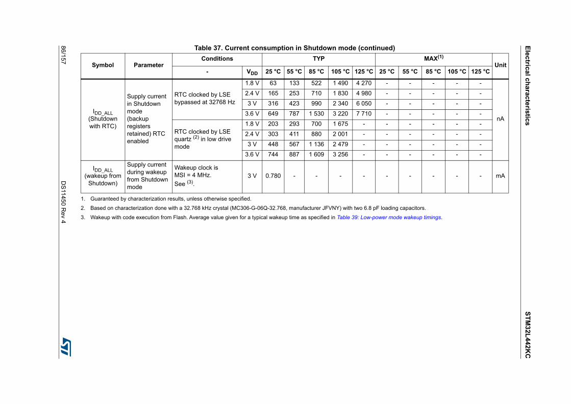
Elec
trical c
hara
cteristic
sS
TM
32
L4
42K
C
86/1
57D
S114
50 Rev 4
IDD_ALL(Shutdown with RTC)
Supply current in Shutdown mode (backup registers retained) RTC enabled
RTC clocked by LSE bypassed at 32768 Hz
1.8 V 63 133 522 1 490 4 270 - - - - -
nA
2.4 V 165 253 710 1 830 4 980 - - - - -
3 V 316 423 990 2 340 6 050 - - - - -
3.6 V 649 787 1 530 3 220 7 710 - - - - -
RTC clocked by LSE quartz (2) in low drive mode
1.8 V 203 293 700 1 675 - - - - - -
2.4 V 303 411 880 2 001 - - - - - -
3 V 448 567 1 136 2 479 - - - - - -
3.6 V 744 887 1 609 3 256 - - - - - -
IDD_ALL(wakeup from
Shutdown)
Supply current during wakeup from Shutdown mode
Wakeup clock is MSI = 4 MHz.
See (3).3 V 0.780 - - - - - - - - - mA
1. Guaranteed by characterization results, unless otherwise specified.
2. Based on characterization done with a 32.768 kHz crystal (MC306-G-06Q-32.768, manufacturer JFVNY) with two 6.8 pF loading capacitors.
3. Wakeup with code execution from Flash. Average value given for a typical wakeup time as specified in Table 39: Low-power mode wakeup timings.
Table 37. Current consumption in Shutdown mode (continued)
Symbol ParameterConditions TYP MAX(1)
Unit- VDD 25 °C 55 °C 85 °C 105 °C 125 °C 25 °C 55 °C 85 °C 105 °C 125 °C
DS11450 Rev 4 87/157
STM32L442KC Electrical characteristics
149
I/O system current consumption
The current consumption of the I/O system has two components: static and dynamic.
I/O static current consumption
All the I/Os used as inputs with pull-up generate current consumption when the pin is externally held low. The value of this current consumption can be simply computed by using the pull-up/pull-down resistors values given in Table 57: I/O static characteristics.
For the output pins, any external pull-down or external load must also be considered to estimate the current consumption.
Additional I/O current consumption is due to I/Os configured as inputs if an intermediate voltage level is externally applied. This current consumption is caused by the input Schmitt trigger circuits used to discriminate the input value. Unless this specific configuration is required by the application, this supply current consumption can be avoided by configuring these I/Os in analog mode. This is notably the case of ADC input pins which should be configured as analog inputs.
Caution: Any floating input pin can also settle to an intermediate voltage level or switch inadvertently, as a result of external electromagnetic noise. To avoid current consumption related to floating pins, they must either be configured in analog mode, or forced internally to a definite digital value. This can be done either by using pull-up/down resistors or by configuring the pins in output mode.
I/O dynamic current consumption
In addition to the internal peripheral current consumption measured previously (see Table 38: Peripheral current consumption), the I/Os used by an application also contribute to the current consumption. When an I/O pin switches, it uses the current from the I/O supply voltage to supply the I/O pin circuitry and to charge/discharge the capacitive load (internal or external) connected to the pin:
where
ISW is the current sunk by a switching I/O to charge/discharge the capacitive load
VDDIOx is the I/O supply voltage
fSW is the I/O switching frequency
C is the total capacitance seen by the I/O pin: C = CINT+ CEXT + CS
CS is the PCB board capacitance including the pad pin.
The test pin is configured in push-pull output mode and is toggled by software at a fixed frequency.
ISW VDDIOx fSW C××=

Electrical characteristics STM32L442KC
88/157 DS11450 Rev 4
On-chip peripheral current consumption
The current consumption of the on-chip peripherals is given in Table 38. The MCU is placed under the following conditions:
• All I/O pins are in Analog mode
• The given value is calculated by measuring the difference of the current consumptions:
– when the peripheral is clocked on
– when the peripheral is clocked off
• Ambient operating temperature and supply voltage conditions summarized in Table 18: Voltage characteristics
• The power consumption of the digital part of the on-chip peripherals is given in Table 38. The power consumption of the analog part of the peripherals (where applicable) is indicated in each related section of the datasheet.
Table 38. Peripheral current consumption
Peripheral Range 1 Range 2Low-power run
and sleepUnit
AHB
Bus Matrix(1) 3.2 2.9 3.1
µA/MHz
ADC independent clock domain 0.4 0.1 0.2
ADC clock domain 2.1 1.9 1.9
AES 1.7 1.5 1.6
CRC 0.4 0.2 0.3
DMA1 1.4 1.3 1.4
DMA2 1.5 1.3 1.4
FLASH 6.2 5.2 5.8
GPIOA(2) 1.7 1.4 1.6
GPIOB(2)) 1.6 1.3 1.6
GPIOC(2) 1.7 1.5 1.6
GPIOH(2) 0.6 0.6 0.5
QSPI 7.0 5.8 7.3
RNG independent clock domain 2.2 N/A N/A
RNG clock domain 0.5 N/A N/A
SRAM1 0.8 0.9 0.7
SRAM2 1.0 0.8 0.8
TSC 1.6 1.3 1.3
All AHB Peripherals 21.7 18.5 20.3
APB1
AHB to APB1 bridge(3) 0.9 0.7 0.9
CAN1 4.1 3.2 3.9
DAC1 2.4 1.8 2.2
RTCA 1.7 1.1 2.1
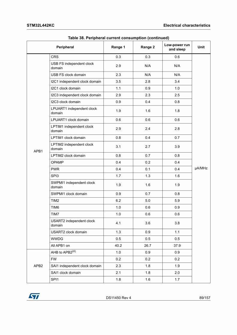
DS11450 Rev 4 89/157
STM32L442KC Electrical characteristics
149
APB1
CRS 0.3 0.3 0.6
µA/MHz
USB FS independent clock domain
2.9 N/A N/A
USB FS clock domain 2.3 N/A N/A
I2C1 independent clock domain 3.5 2.8 3.4
I2C1 clock domain 1.1 0.9 1.0
I2C3 independent clock domain 2.9 2.3 2.5
I2C3 clock domain 0.9 0.4 0.8
LPUART1 independent clock domain
1.9 1.6 1.8
LPUART1 clock domain 0.6 0.6 0.6
LPTIM1 independent clock domain
2.9 2.4 2.8
LPTIM1 clock domain 0.8 0.4 0.7
LPTIM2 independent clock domain
3.1 2.7 3.9
LPTIM2 clock domain 0.8 0.7 0.8
OPAMP 0.4 0.2 0.4
PWR 0.4 0.1 0.4
SPI3 1.7 1.3 1.6
SWPMI1 independent clock domain
1.9 1.6 1.9
SWPMI1 clock domain 0.9 0.7 0.8
TIM2 6.2 5.0 5.9
TIM6 1.0 0.6 0.9
TIM7 1.0 0.6 0.6
USART2 independent clock domain
4.1 3.6 3.8
USART2 clock domain 1.3 0.9 1.1
WWDG 0.5 0.5 0.5
All APB1 on 40.2 26.7 37.9
APB2
AHB to APB2(4) 1.0 0.9 0.9
FW 0.2 0.2 0.2
SAI1 independent clock domain 2.3 1.8 1.9
SAI1 clock domain 2.1 1.8 2.0
SPI1 1.8 1.6 1.7
Table 38. Peripheral current consumption (continued)
Peripheral Range 1 Range 2Low-power run
and sleepUnit
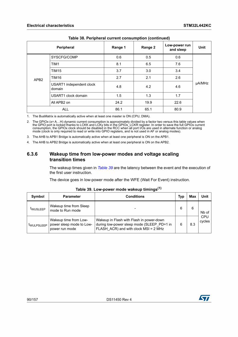
Electrical characteristics STM32L442KC
90/157 DS11450 Rev 4
6.3.6 Wakeup time from low-power modes and voltage scaling transition times
The wakeup times given in Table 39 are the latency between the event and the execution of the first user instruction.
The device goes in low-power mode after the WFE (Wait For Event) instruction.
APB2
SYSCFG/COMP 0.6 0.5 0.6
µA/MHz
TIM1 8.1 6.5 7.6
TIM15 3.7 3.0 3.4
TIM16 2.7 2.1 2.6
USART1 independent clock domain
4.8 4.2 4.6
USART1 clock domain 1.5 1.3 1.7
All APB2 on 24.2 19.9 22.6
ALL 86.1 65.1 80.9
1. The BusMatrix is automatically active when at least one master is ON (CPU, DMA).
2. The GPIOx (x= A…H) dynamic current consumption is approximately divided by a factor two versus this table values when the GPIO port is locked thanks to LCKK and LCKy bits in the GPIOx_LCKR register. In order to save the full GPIOx current consumption, the GPIOx clock should be disabled in the RCC when all port I/Os are used in alternate function or analog mode (clock is only required to read or write into GPIO registers, and is not used in AF or analog modes).
3. The AHB to APB1 Bridge is automatically active when at least one peripheral is ON on the APB1.
4. The AHB to APB2 Bridge is automatically active when at least one peripheral is ON on the APB2.
Table 38. Peripheral current consumption (continued)
Peripheral Range 1 Range 2Low-power run
and sleepUnit
Table 39. Low-power mode wakeup timings(1)
Symbol Parameter Conditions Typ Max Unit
tWUSLEEPWakeup time from Sleep mode to Run mode
- 6 6Nb of CPU
cyclestWULPSLEEP
Wakeup time from Low-power sleep mode to Low-power run mode
Wakeup in Flash with Flash in power-down during low-power sleep mode (SLEEP_PD=1 in FLASH_ACR) and with clock MSI = 2 MHz
6 8.3
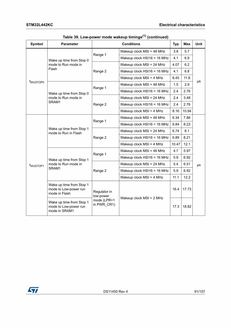
DS11450 Rev 4 91/157
STM32L442KC Electrical characteristics
149
tWUSTOP0
Wake up time from Stop 0 mode to Run mode in Flash
Range 1Wakeup clock MSI = 48 MHz 3.8 5.7
µs
Wakeup clock HSI16 = 16 MHz 4.1 6.9
Range 2
Wakeup clock MSI = 24 MHz 4.07 6.2
Wakeup clock HSI16 = 16 MHz 4.1 6.8
Wakeup clock MSI = 4 MHz 8.45 11.8
Wake up time from Stop 0 mode to Run mode in SRAM1
Range 1Wakeup clock MSI = 48 MHz 1.5 2.9
Wakeup clock HSI16 = 16 MHz 2.4 2.76
Range 2
Wakeup clock MSI = 24 MHz 2.4 3.48
Wakeup clock HSI16 = 16 MHz 2.4 2.76
Wakeup clock MSI = 4 MHz 8.16 10.94
tWUSTOP1
Wake up time from Stop 1 mode to Run in Flash
Range 1Wakeup clock MSI = 48 MHz 6.34 7.86
µs
Wakeup clock HSI16 = 16 MHz 6.84 8.23
Range 2
Wakeup clock MSI = 24 MHz 6.74 8.1
Wakeup clock HSI16 = 16 MHz 6.89 8.21
Wakeup clock MSI = 4 MHz 10.47 12.1
Wake up time from Stop 1 mode to Run mode in SRAM1
Range 1Wakeup clock MSI = 48 MHz 4.7 5.97
Wakeup clock HSI16 = 16 MHz 5.9 6.92
Range 2
Wakeup clock MSI = 24 MHz 5.4 6.51
Wakeup clock HSI16 = 16 MHz 5.9 6.92
Wakeup clock MSI = 4 MHz 11.1 12.2
Wake up time from Stop 1 mode to Low-power run mode in Flash Regulator in
low-power mode (LPR=1 in PWR_CR1)
Wakeup clock MSI = 2 MHz
16.4 17.73
Wake up time from Stop 1 mode to Low-power run mode in SRAM1
17.3 18.82
Table 39. Low-power mode wakeup timings(1) (continued)
Symbol Parameter Conditions Typ Max Unit
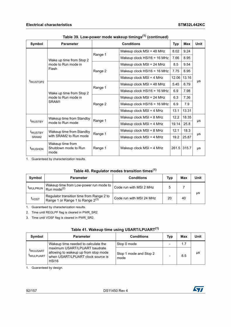
Electrical characteristics STM32L442KC
92/157 DS11450 Rev 4
tWUSTOP2
Wake up time from Stop 2 mode to Run mode in Flash
Range 1Wakeup clock MSI = 48 MHz 8.02 9.24
µs
Wakeup clock HSI16 = 16 MHz 7.66 8.95
Range 2
Wakeup clock MSI = 24 MHz 8.5 9.54
Wakeup clock HSI16 = 16 MHz 7.75 8.95
Wakeup clock MSI = 4 MHz 12.06 13.16
Wake up time from Stop 2 mode to Run mode in SRAM1
Range 1Wakeup clock MSI = 48 MHz 5.45 6.79
Wakeup clock HSI16 = 16 MHz 6.9 7.98
Range 2
Wakeup clock MSI = 24 MHz 6.3 7.36
Wakeup clock HSI16 = 16 MHz 6.9 7.9
Wakeup clock MSI = 4 MHz 13.1 13.31
tWUSTBYWakeup time from Standby mode to Run mode
Range 1Wakeup clock MSI = 8 MHz 12.2 18.35
µsWakeup clock MSI = 4 MHz 19.14 25.8
tWUSTBY
SRAM2
Wakeup time from Standby with SRAM2 to Run mode
Range 1Wakeup clock MSI = 8 MHz 12.1 18.3
µsWakeup clock MSI = 4 MHz 19.2 25.87
tWUSHDN
Wakeup time from Shutdown mode to Run mode
Range 1 Wakeup clock MSI = 4 MHz 261.5 315.7 µs
1. Guaranteed by characterization results.
Table 39. Low-power mode wakeup timings(1) (continued)
Symbol Parameter Conditions Typ Max Unit
Table 40. Regulator modes transition times(1)
Symbol Parameter Conditions Typ Max Unit
tWULPRUNWakeup time from Low-power run mode to Run mode(2) Code run with MSI 2 MHz 5 7
µs
tVOSTRegulator transition time from Range 2 to Range 1 or Range 1 to Range 2(3) Code run with MSI 24 MHz 20 40
1. Guaranteed by characterization results.
2. Time until REGLPF flag is cleared in PWR_SR2.
3. Time until VOSF flag is cleared in PWR_SR2.
Table 41. Wakeup time using USART/LPUART(1)
Symbol Parameter Conditions Typ Max Unit
tWUUSART
tWULPUART
Wakeup time needed to calculate the maximum USART/LPUART baudrate allowing to wakeup up from stop mode when USART/LPUART clock source is HSI16
Stop 0 mode - 1.7
µsStop 1 mode and Stop 2 mode
- 8.5
1. Guaranteed by design.

DS11450 Rev 4 93/157
STM32L442KC Electrical characteristics
149
6.3.7 External clock source characteristics
High-speed external user clock generated from an external source
In bypass mode the HSE oscillator is switched off and the input pin is a standard GPIO.
The external clock signal has to respect the I/O characteristics in Section 6.3.14. However, the recommended clock input waveform is shown in Figure 12: High-speed external clock source AC timing diagram.
Figure 12. High-speed external clock source AC timing diagram
Table 42. High-speed external user clock characteristics(1)
Symbol Parameter Conditions Min Typ Max Unit
fHSE_ext User external clock source frequency
Voltage scaling Range 1
- 8 48
MHzVoltage scaling Range 2
- 8 26
VHSEH CK_IN input pin high level voltage - 0.7 VDDIOx - VDDIOxV
VHSEL CK_IN input pin low level voltage - VSS - 0.3 VDDIOx
tw(HSEH)tw(HSEL)
CK_IN high or low time
Voltage scaling Range 1
7 - -
nsVoltage scaling Range 2
18 - -
1. Guaranteed by design.
MS19214V2
VHSEH
tf(HSE)
90%10%
THSE
ttr(HSE)
VHSEL
tw(HSEH)
tw(HSEL)
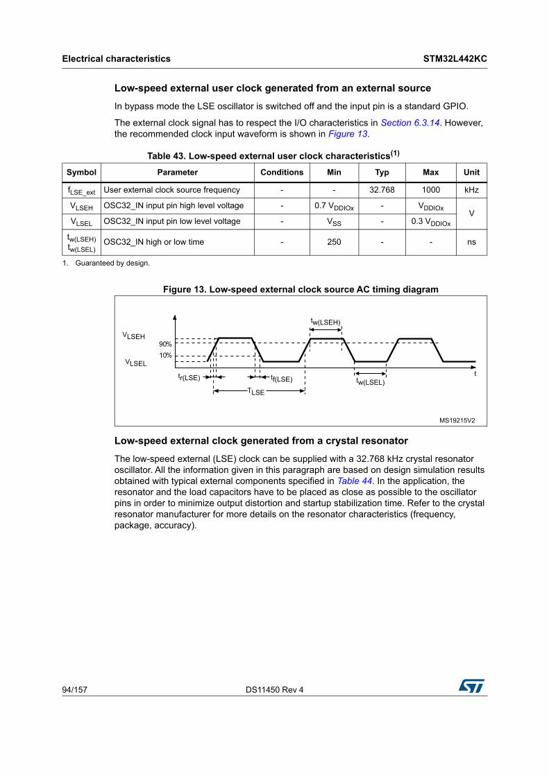
Electrical characteristics STM32L442KC
94/157 DS11450 Rev 4
Low-speed external user clock generated from an external source
In bypass mode the LSE oscillator is switched off and the input pin is a standard GPIO.
The external clock signal has to respect the I/O characteristics in Section 6.3.14. However, the recommended clock input waveform is shown in Figure 13.
Figure 13. Low-speed external clock source AC timing diagram
Low-speed external clock generated from a crystal resonator
The low-speed external (LSE) clock can be supplied with a 32.768 kHz crystal resonator oscillator. All the information given in this paragraph are based on design simulation results obtained with typical external components specified in Table 44. In the application, the resonator and the load capacitors have to be placed as close as possible to the oscillator pins in order to minimize output distortion and startup stabilization time. Refer to the crystal resonator manufacturer for more details on the resonator characteristics (frequency, package, accuracy).
Table 43. Low-speed external user clock characteristics(1)
Symbol Parameter Conditions Min Typ Max Unit
fLSE_ext User external clock source frequency - - 32.768 1000 kHz
VLSEH OSC32_IN input pin high level voltage - 0.7 VDDIOx - VDDIOxV
VLSEL OSC32_IN input pin low level voltage - VSS - 0.3 VDDIOx
tw(LSEH)tw(LSEL)
OSC32_IN high or low time - 250 - - ns
1. Guaranteed by design.
MS19215V2
VLSEH
tf(LSE)
90%10%
TLSE
ttr(LSE)
VLSEL
tw(LSEH)
tw(LSEL)
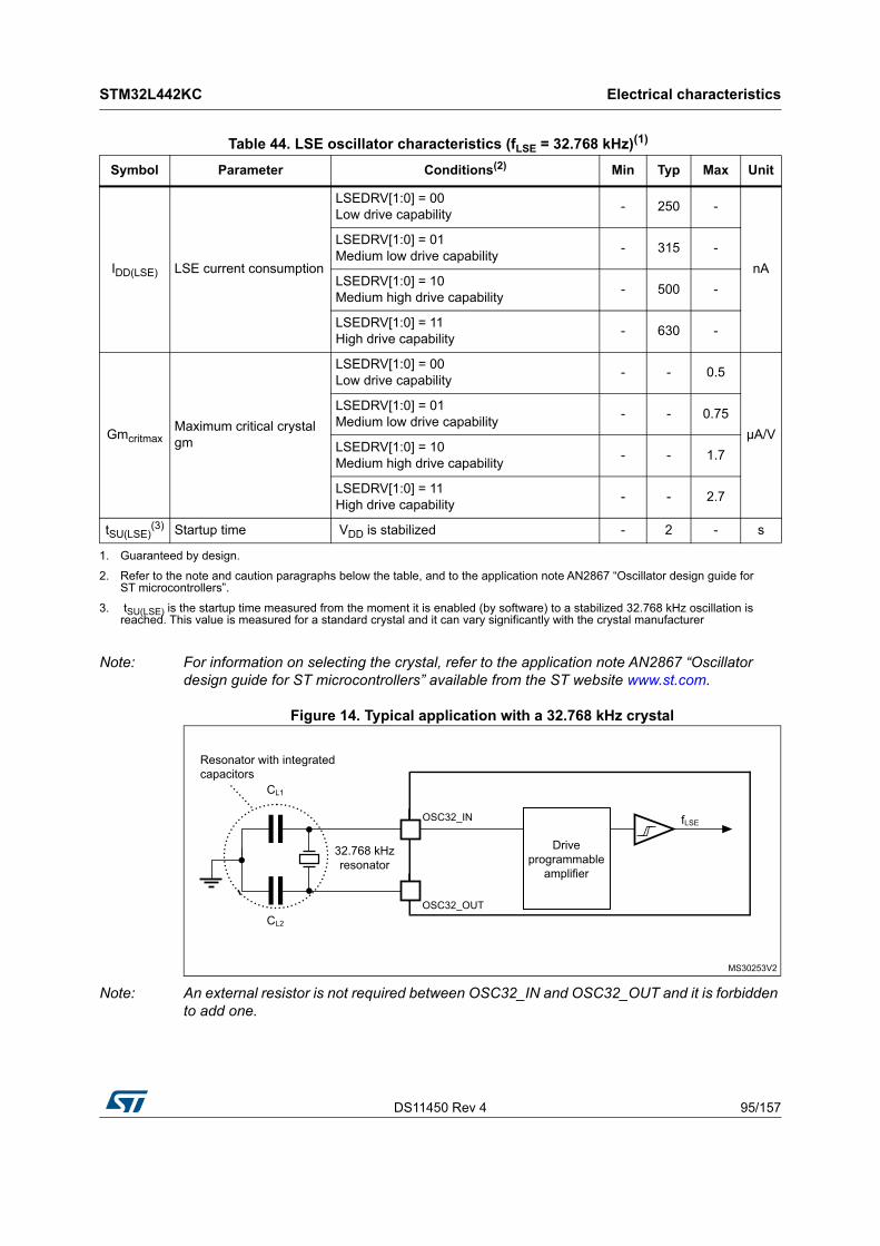
DS11450 Rev 4 95/157
STM32L442KC Electrical characteristics
149
Note: For information on selecting the crystal, refer to the application note AN2867 “Oscillator design guide for ST microcontrollers” available from the ST website www.st.com.
Figure 14. Typical application with a 32.768 kHz crystal
Note: An external resistor is not required between OSC32_IN and OSC32_OUT and it is forbidden to add one.
Table 44. LSE oscillator characteristics (fLSE = 32.768 kHz)(1)
Symbol Parameter Conditions(2) Min Typ Max Unit
IDD(LSE) LSE current consumption
LSEDRV[1:0] = 00 Low drive capability
- 250 -
nA
LSEDRV[1:0] = 01 Medium low drive capability
- 315 -
LSEDRV[1:0] = 10 Medium high drive capability
- 500 -
LSEDRV[1:0] = 11 High drive capability
- 630 -
GmcritmaxMaximum critical crystal gm
LSEDRV[1:0] = 00 Low drive capability
- - 0.5
µA/V
LSEDRV[1:0] = 01 Medium low drive capability
- - 0.75
LSEDRV[1:0] = 10 Medium high drive capability
- - 1.7
LSEDRV[1:0] = 11 High drive capability
- - 2.7
tSU(LSE)(3) Startup time VDD is stabilized - 2 - s
1. Guaranteed by design.
2. Refer to the note and caution paragraphs below the table, and to the application note AN2867 “Oscillator design guide for ST microcontrollers”.
3. tSU(LSE) is the startup time measured from the moment it is enabled (by software) to a stabilized 32.768 kHz oscillation is reached. This value is measured for a standard crystal and it can vary significantly with the crystal manufacturer
MS30253V2
OSC32_IN
OSC32_OUT
Drive programmable
amplifier
fLSE
32.768 kHz resonator
Resonator with integrated capacitors
CL1
CL2
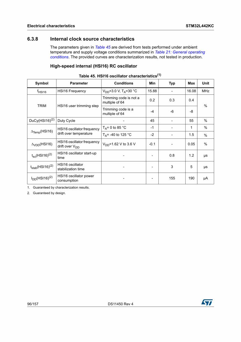
Electrical characteristics STM32L442KC
96/157 DS11450 Rev 4
6.3.8 Internal clock source characteristics
The parameters given in Table 45 are derived from tests performed under ambient temperature and supply voltage conditions summarized in Table 21: General operating conditions. The provided curves are characterization results, not tested in production.
High-speed internal (HSI16) RC oscillator
Table 45. HSI16 oscillator characteristics(1)
Symbol Parameter Conditions Min Typ Max Unit
fHSI16 HSI16 Frequency VDD=3.0 V, TA=30 °C 15.88 - 16.08 MHz
TRIM HSI16 user trimming step
Trimming code is not a multiple of 64
0.2 0.3 0.4
%Trimming code is a multiple of 64
-4 -6 -8
DuCy(HSI16)(2) Duty Cycle - 45 - 55 %
∆Temp(HSI16)HSI16 oscillator frequency drift over temperature
TA= 0 to 85 °C -1 - 1 %
TA= -40 to 125 °C -2 - 1.5 %
∆VDD(HSI16)HSI16 oscillator frequency drift over VDD
VDD=1.62 V to 3.6 V -0.1 - 0.05 %
tsu(HSI16)(2) HSI16 oscillator start-up time
- - 0.8 1.2 μs
tstab(HSI16)(2) HSI16 oscillator stabilization time
- - 3 5 μs
IDD(HSI16)(2) HSI16 oscillator power consumption
- - 155 190 μA
1. Guaranteed by characterization results.
2. Guaranteed by design.
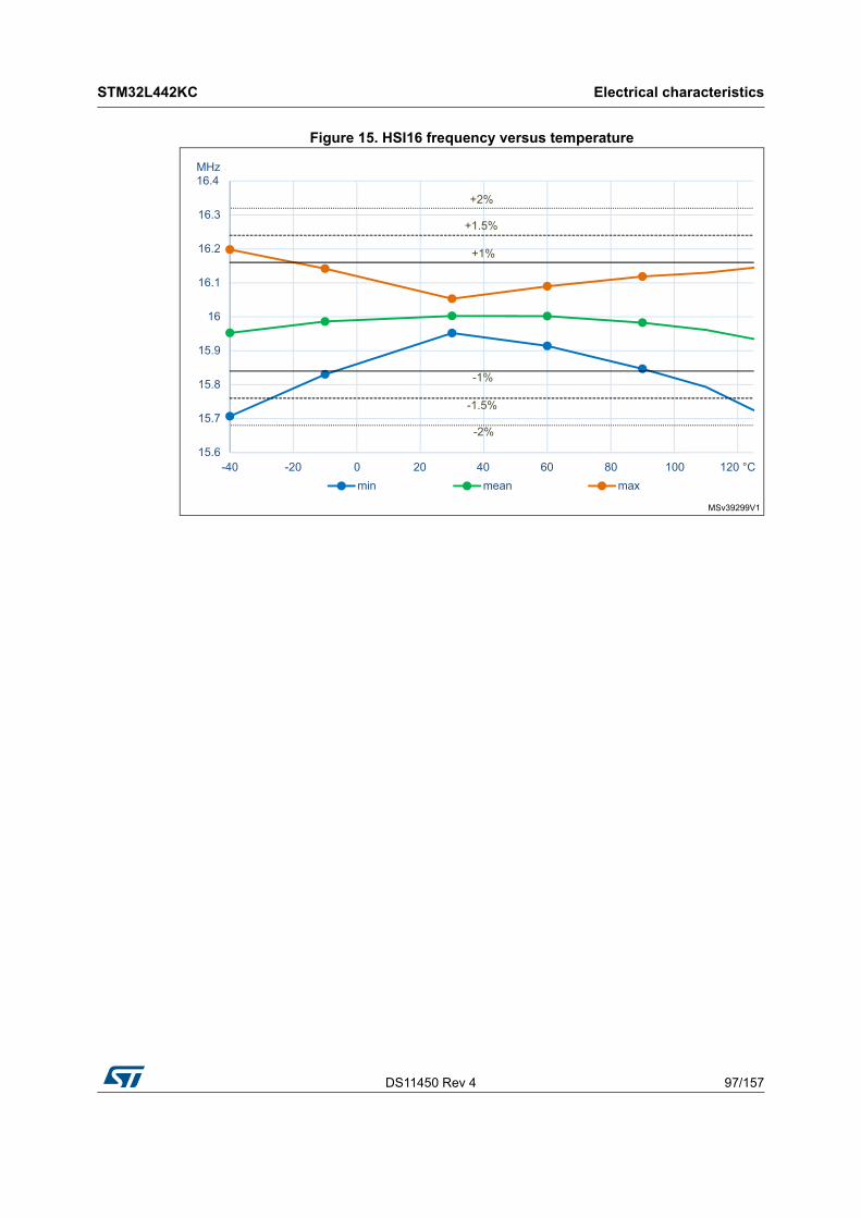
DS11450 Rev 4 97/157
STM32L442KC Electrical characteristics
149
Figure 15. HSI16 frequency versus temperature
MSv39299V1
15.6
15.7
15.8
15.9
16
16.1
16.2
16.3
16.4MHz
min mean max
+1%
-1%
+2%
-2%
+1.5%
-1.5%
-40 -20 0 20 40 60 80 100 120 °C
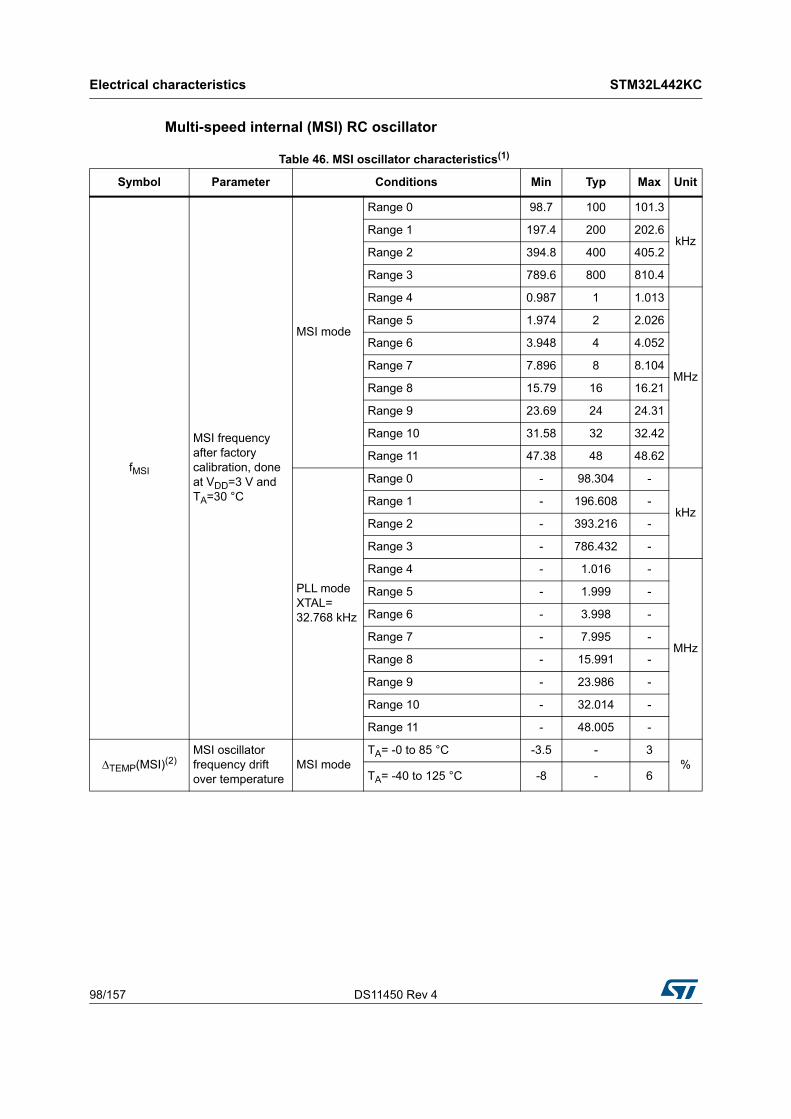
Electrical characteristics STM32L442KC
98/157 DS11450 Rev 4
Multi-speed internal (MSI) RC oscillator
Table 46. MSI oscillator characteristics(1)
Symbol Parameter Conditions Min Typ Max Unit
fMSI
MSI frequency after factory calibration, done at VDD=3 V and TA=30 °C
MSI mode
Range 0 98.7 100 101.3
kHzRange 1 197.4 200 202.6
Range 2 394.8 400 405.2
Range 3 789.6 800 810.4
Range 4 0.987 1 1.013
MHz
Range 5 1.974 2 2.026
Range 6 3.948 4 4.052
Range 7 7.896 8 8.104
Range 8 15.79 16 16.21
Range 9 23.69 24 24.31
Range 10 31.58 32 32.42
Range 11 47.38 48 48.62
PLL mode XTAL= 32.768 kHz
Range 0 - 98.304 -
kHzRange 1 - 196.608 -
Range 2 - 393.216 -
Range 3 - 786.432 -
Range 4 - 1.016 -
MHz
Range 5 - 1.999 -
Range 6 - 3.998 -
Range 7 - 7.995 -
Range 8 - 15.991 -
Range 9 - 23.986 -
Range 10 - 32.014 -
Range 11 - 48.005 -
∆TEMP(MSI)(2)MSI oscillator frequency drift over temperature
MSI modeTA= -0 to 85 °C -3.5 - 3
%TA= -40 to 125 °C -8 - 6
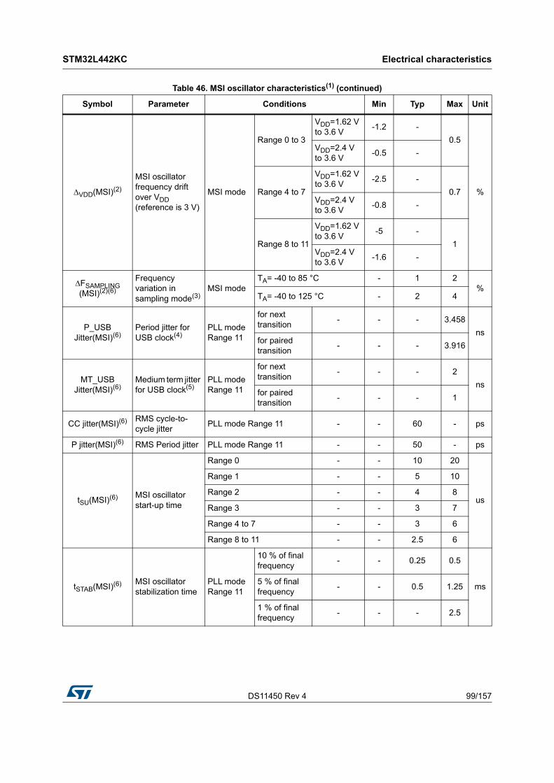
DS11450 Rev 4 99/157
STM32L442KC Electrical characteristics
149
∆VDD(MSI)(2)
MSI oscillator frequency drift over VDD (reference is 3 V)
MSI mode
Range 0 to 3
VDD=1.62 V to 3.6 V
-1.2 -
0.5
%
VDD=2.4 V to 3.6 V
-0.5 -
Range 4 to 7
VDD=1.62 V to 3.6 V
-2.5 -
0.7VDD=2.4 V to 3.6 V
-0.8 -
Range 8 to 11
VDD=1.62 V to 3.6 V
-5 -
1VDD=2.4 V to 3.6 V
-1.6 -
∆FSAMPLING(MSI)(2)(6)
Frequency variation in sampling mode(3)
MSI modeTA= -40 to 85 °C - 1 2
%TA= -40 to 125 °C - 2 4
P_USB Jitter(MSI)(6)
Period jitter for USB clock(4)
PLL mode Range 11
for next transition
- - - 3.458
nsfor paired transition
- - - 3.916
MT_USB Jitter(MSI)(6)
Medium term jitter for USB clock(5)
PLL mode Range 11
for next transition
- - - 2
nsfor paired transition
- - - 1
CC jitter(MSI)(6) RMS cycle-to-cycle jitter
PLL mode Range 11 - - 60 - ps
P jitter(MSI)(6) RMS Period jitter PLL mode Range 11 - - 50 - ps
tSU(MSI)(6) MSI oscillator start-up time
Range 0 - - 10 20
us
Range 1 - - 5 10
Range 2 - - 4 8
Range 3 - - 3 7
Range 4 to 7 - - 3 6
Range 8 to 11 - - 2.5 6
tSTAB(MSI)(6) MSI oscillator stabilization time
PLL mode Range 11
10 % of final frequency
- - 0.25 0.5
ms5 % of final frequency
- - 0.5 1.25
1 % of final frequency
- - - 2.5
Table 46. MSI oscillator characteristics(1) (continued)
Symbol Parameter Conditions Min Typ Max Unit
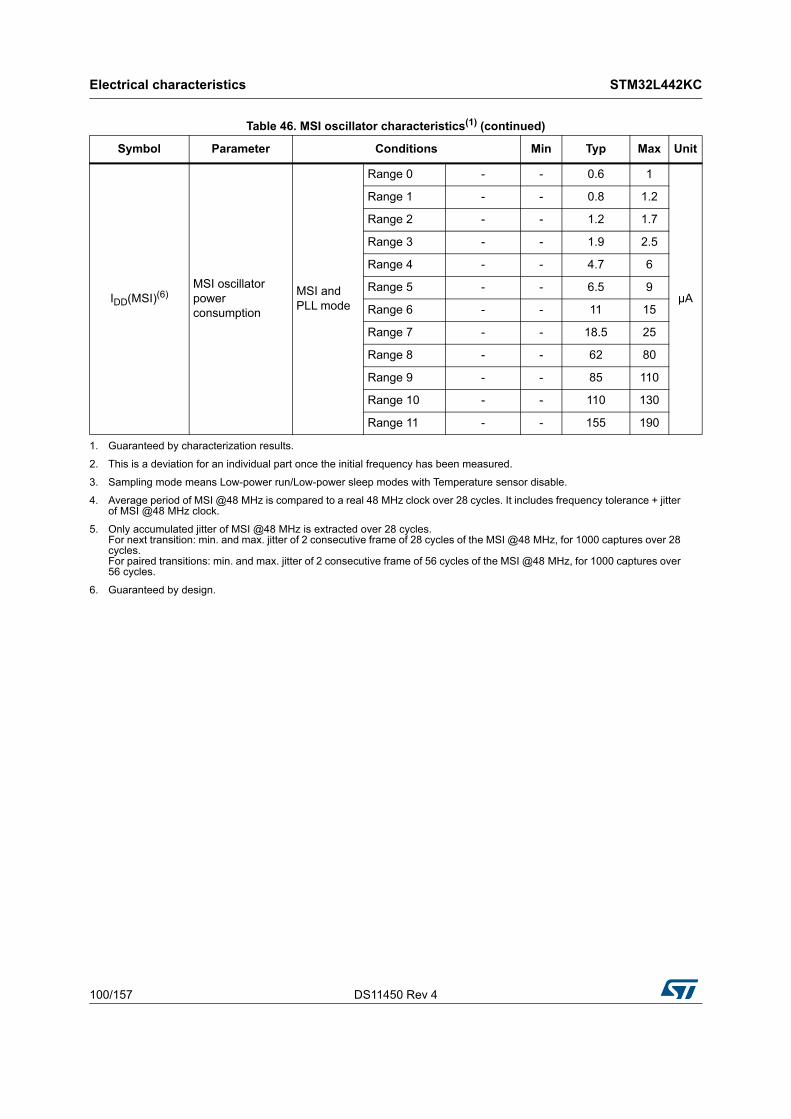
Electrical characteristics STM32L442KC
100/157 DS11450 Rev 4
IDD(MSI)(6)MSI oscillator power consumption
MSI and PLL mode
Range 0 - - 0.6 1
µA
Range 1 - - 0.8 1.2
Range 2 - - 1.2 1.7
Range 3 - - 1.9 2.5
Range 4 - - 4.7 6
Range 5 - - 6.5 9
Range 6 - - 11 15
Range 7 - - 18.5 25
Range 8 - - 62 80
Range 9 - - 85 110
Range 10 - - 110 130
Range 11 - - 155 190
1. Guaranteed by characterization results.
2. This is a deviation for an individual part once the initial frequency has been measured.
3. Sampling mode means Low-power run/Low-power sleep modes with Temperature sensor disable.
4. Average period of MSI @48 MHz is compared to a real 48 MHz clock over 28 cycles. It includes frequency tolerance + jitter of MSI @48 MHz clock.
5. Only accumulated jitter of MSI @48 MHz is extracted over 28 cycles. For next transition: min. and max. jitter of 2 consecutive frame of 28 cycles of the MSI @48 MHz, for 1000 captures over 28 cycles. For paired transitions: min. and max. jitter of 2 consecutive frame of 56 cycles of the MSI @48 MHz, for 1000 captures over 56 cycles.
6. Guaranteed by design.
Table 46. MSI oscillator characteristics(1) (continued)
Symbol Parameter Conditions Min Typ Max Unit
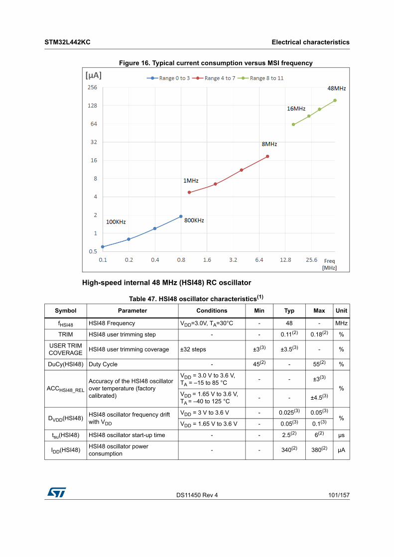
DS11450 Rev 4 101/157
STM32L442KC Electrical characteristics
149
Figure 16. Typical current consumption versus MSI frequency
High-speed internal 48 MHz (HSI48) RC oscillator
Table 47. HSI48 oscillator characteristics(1)
Symbol Parameter Conditions Min Typ Max Unit
fHSI48 HSI48 Frequency VDD=3.0V, TA=30°C - 48 - MHz
TRIM HSI48 user trimming step - - 0.11(2) 0.18(2) %
USER TRIM COVERAGE
HSI48 user trimming coverage ±32 steps ±3(3) ±3.5(3) - %
DuCy(HSI48) Duty Cycle - 45(2) - 55(2) %
ACCHSI48_REL
Accuracy of the HSI48 oscillator over temperature (factory calibrated)
VDD = 3.0 V to 3.6 V, TA = –15 to 85 °C
- - ±3(3)
%VDD = 1.65 V to 3.6 V, TA = –40 to 125 °C
- - ±4.5(3)
DVDD(HSI48)HSI48 oscillator frequency drift with VDD
VDD = 3 V to 3.6 V - 0.025(3) 0.05(3)
%VDD = 1.65 V to 3.6 V - 0.05(3) 0.1(3)
tsu(HSI48) HSI48 oscillator start-up time - - 2.5(2) 6(2) μs
IDD(HSI48)HSI48 oscillator power consumption
- - 340(2) 380(2) μA
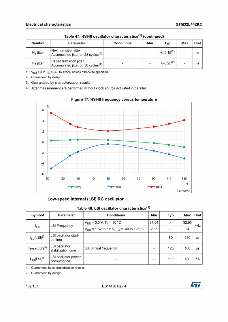
Electrical characteristics STM32L442KC
102/157 DS11450 Rev 4
Figure 17. HSI48 frequency versus temperature
Low-speed internal (LSI) RC oscillator
NT jitterNext transition jitter Accumulated jitter on 28 cycles(4) - - +/-0.15(2) - ns
PT jitterPaired transition jitter Accumulated jitter on 56 cycles(4) - - +/-0.25(2) - ns
1. VDD = 3 V, TA = –40 to 125°C unless otherwise specified.
2. Guaranteed by design.
3. Guaranteed by characterization results.
4. Jitter measurement are performed without clock source activated in parallel.
Table 47. HSI48 oscillator characteristics(1) (continued)
Symbol Parameter Conditions Min Typ Max Unit
MSv40989V1
-6
-4
-2
0
2
4
6
-50 -30 -10 10 30 50 70 90 110 130
Avg min max°C
%
Table 48. LSI oscillator characteristics(1)
Symbol Parameter Conditions Min Typ Max Unit
fLSI LSI FrequencyVDD = 3.0 V, TA = 30 °C 31.04 - 32.96
kHzVDD = 1.62 to 3.6 V, TA = -40 to 125 °C 29.5 - 34
tSU(LSI)(2) LSI oscillator start-up time
- - 80 130 μs
tSTAB(LSI)(2) LSI oscillator stabilization time
5% of final frequency - 125 180 μs
IDD(LSI)(2) LSI oscillator power consumption
- - 110 180 nA
1. Guaranteed by characterization results.
2. Guaranteed by design.
DS11450 Rev 4 103/157
STM32L442KC Electrical characteristics
149
6.3.9 PLL characteristics
The parameters given in Table 49 are derived from tests performed under temperature and VDD supply voltage conditions summarized in Table 21: General operating conditions.
Table 49. PLL, PLLSAI1 characteristics(1)
Symbol Parameter Conditions Min Typ Max Unit
fPLL_IN
PLL input clock(2) - 4 - 16 MHz
PLL input clock duty cycle - 45 - 55 %
fPLL_P_OUT PLL multiplier output clock PVoltage scaling Range 1 3.0968 - 80
MHzVoltage scaling Range 2 3.0968 - 26
fPLL_Q_OUT PLL multiplier output clock QVoltage scaling Range 1 12 - 80
MHzVoltage scaling Range 2 12 - 26
fPLL_R_OUT PLL multiplier output clock RVoltage scaling Range 1 12 - 80
MHzVoltage scaling Range 2 12 - 26
fVCO_OUT PLL VCO outputVoltage scaling Range 1 96 - 344
MHzVoltage scaling Range 2 96 - 128
tLOCK PLL lock time - - 15 40 μs
JitterRMS cycle-to-cycle jitter
System clock 80 MHz- 40 -
±psRMS period jitter - 30 -
IDD(PLL)PLL power consumption on VDD
(1)
VCO freq = 96 MHz - 200 260
μAVCO freq = 192 MHz - 300 380
VCO freq = 344 MHz - 520 650
1. Guaranteed by design.
2. Take care of using the appropriate division factor M to obtain the specified PLL input clock values. The M factor is shared between the 2 PLLs.
Electrical characteristics STM32L442KC
104/157 DS11450 Rev 4
6.3.10 Flash memory characteristics
Table 50. Flash memory characteristics(1)
1. Guaranteed by design.
Symbol Parameter Conditions Typ Max Unit
tprog 64-bit programming time - 81.69 90.76 µs
tprog_rowone row (32 double word) programming time
normal programming 2.61 2.90
ms
fast programming 1.91 2.12
tprog_pageone page (2 Kbyte) programming time
normal programming 20.91 23.24
fast programming 15.29 16.98
tERASE Page (2 KB) erase time - 22.02 24.47
tprog_bankone bank (512 Kbyte) programming time
normal programming 5.35 5.95s
fast programming 3.91 4.35
tMEMass erase time (one or two banks)
- 22.13 24.59 ms
IDD
Average consumption from VDD
Write mode 3.4 -
mAErase mode 3.4 -
Maximum current (peak)Write mode 7 (for 2 μs) -
Erase mode 7 (for 41 μs) -
Table 51. Flash memory endurance and data retention
Symbol Parameter Conditions Min(1)
1. Guaranteed by characterization results.
Unit
NEND Endurance TA = –40 to +105 °C 10 kcycles
tRET Data retention
1 kcycle(2) at TA = 85 °C
2. Cycling performed over the whole temperature range.
30
Years
1 kcycle(2) at TA = 105 °C 15
1 kcycle(2) at TA = 125 °C 7
10 kcycles(2) at TA = 55 °C 30
10 kcycles(2) at TA = 85 °C 15
10 kcycles(2) at TA = 105 °C 10
DS11450 Rev 4 105/157
STM32L442KC Electrical characteristics
149
6.3.11 EMC characteristics
Susceptibility tests are performed on a sample basis during device characterization.
Functional EMS (electromagnetic susceptibility)
While a simple application is executed on the device (toggling 2 LEDs through I/O ports). the device is stressed by two electromagnetic events until a failure occurs. The failure is indicated by the LEDs:
• Electrostatic discharge (ESD) (positive and negative) is applied to all device pins until a functional disturbance occurs. This test is compliant with the IEC 61000-4-2 standard.
• FTB: A Burst of Fast Transient voltage (positive and negative) is applied to VDD and VSS through a 100 pF capacitor, until a functional disturbance occurs. This test is compliant with the IEC 61000-4-4 standard.
A device reset allows normal operations to be resumed.
The test results are given in Table 52. They are based on the EMS levels and classes defined in application note AN1709.
Designing hardened software to avoid noise problems
EMC characterization and optimization are performed at component level with a typical application environment and simplified MCU software. It should be noted that good EMC performance is highly dependent on the user application and the software in particular.
Therefore it is recommended that the user applies EMC software optimization and prequalification tests in relation with the EMC level requested for his application.
Software recommendations
The software flowchart must include the management of runaway conditions such as:
• Corrupted program counter
• Unexpected reset
• Critical Data corruption (control registers...)
Table 52. EMS characteristics
Symbol Parameter ConditionsLevel/Class
VFESDVoltage limits to be applied on any I/O pin to induce a functional disturbance
VDD = 3.3 V, TA = +25 °C, fHCLK = 80 MHz, conforming to IEC 61000-4-2
2B
VEFTB
Fast transient voltage burst limits to be applied through 100 pF on VDD and VSS pins to induce a functional disturbance
VDD = 3.3 V, TA = +25 °C, fHCLK = 80 MHz, conforming to IEC 61000-4-4
5A
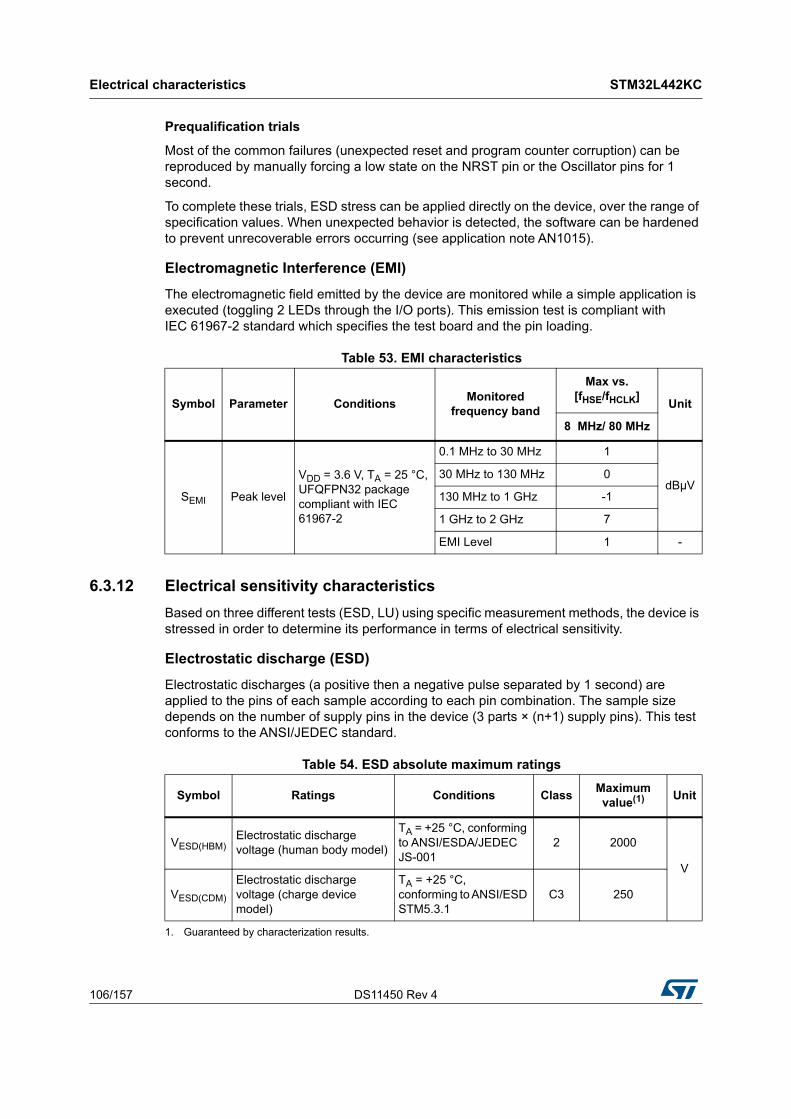
Electrical characteristics STM32L442KC
106/157 DS11450 Rev 4
Prequalification trials
Most of the common failures (unexpected reset and program counter corruption) can be reproduced by manually forcing a low state on the NRST pin or the Oscillator pins for 1 second.
To complete these trials, ESD stress can be applied directly on the device, over the range of specification values. When unexpected behavior is detected, the software can be hardened to prevent unrecoverable errors occurring (see application note AN1015).
Electromagnetic Interference (EMI)
The electromagnetic field emitted by the device are monitored while a simple application is executed (toggling 2 LEDs through the I/O ports). This emission test is compliant with IEC 61967-2 standard which specifies the test board and the pin loading.
6.3.12 Electrical sensitivity characteristics
Based on three different tests (ESD, LU) using specific measurement methods, the device is stressed in order to determine its performance in terms of electrical sensitivity.
Electrostatic discharge (ESD)
Electrostatic discharges (a positive then a negative pulse separated by 1 second) are applied to the pins of each sample according to each pin combination. The sample size depends on the number of supply pins in the device (3 parts × (n+1) supply pins). This test conforms to the ANSI/JEDEC standard.
Table 53. EMI characteristics
Symbol Parameter ConditionsMonitored
frequency band
Max vs. [fHSE/fHCLK]
Unit
8 MHz/ 80 MHz
SEMI Peak level
VDD = 3.6 V, TA = 25 °C, UFQFPN32 package compliant with IEC 61967-2
0.1 MHz to 30 MHz 1
dBµV30 MHz to 130 MHz 0
130 MHz to 1 GHz -1
1 GHz to 2 GHz 7
EMI Level 1 -
Table 54. ESD absolute maximum ratings
Symbol Ratings Conditions ClassMaximum value(1)
1. Guaranteed by characterization results.
Unit
VESD(HBM)Electrostatic discharge voltage (human body model)
TA = +25 °C, conforming to ANSI/ESDA/JEDEC JS-001
2 2000
V
VESD(CDM)
Electrostatic discharge voltage (charge device model)
TA = +25 °C, conforming to ANSI/ESD STM5.3.1
C3 250
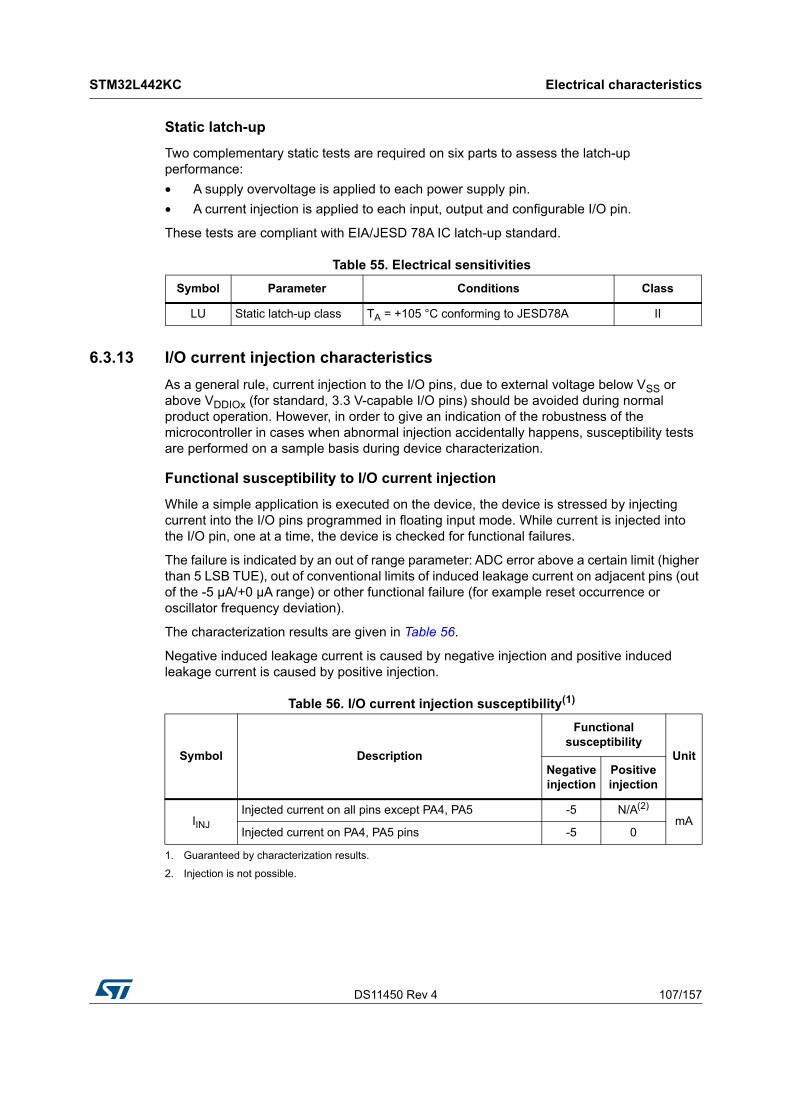
DS11450 Rev 4 107/157
STM32L442KC Electrical characteristics
149
Static latch-up
Two complementary static tests are required on six parts to assess the latch-up performance:
• A supply overvoltage is applied to each power supply pin.
• A current injection is applied to each input, output and configurable I/O pin.
These tests are compliant with EIA/JESD 78A IC latch-up standard.
6.3.13 I/O current injection characteristics
As a general rule, current injection to the I/O pins, due to external voltage below VSS or above VDDIOx (for standard, 3.3 V-capable I/O pins) should be avoided during normal product operation. However, in order to give an indication of the robustness of the microcontroller in cases when abnormal injection accidentally happens, susceptibility tests are performed on a sample basis during device characterization.
Functional susceptibility to I/O current injection
While a simple application is executed on the device, the device is stressed by injecting current into the I/O pins programmed in floating input mode. While current is injected into the I/O pin, one at a time, the device is checked for functional failures.
The failure is indicated by an out of range parameter: ADC error above a certain limit (higher than 5 LSB TUE), out of conventional limits of induced leakage current on adjacent pins (out of the -5 µA/+0 µA range) or other functional failure (for example reset occurrence or oscillator frequency deviation).
The characterization results are given in Table 56.
Negative induced leakage current is caused by negative injection and positive induced leakage current is caused by positive injection.
Table 55. Electrical sensitivities
Symbol Parameter Conditions Class
LU Static latch-up class TA = +105 °C conforming to JESD78A II
Table 56. I/O current injection susceptibility(1)
1. Guaranteed by characterization results.
Symbol Description
Functional susceptibility
UnitNegative injection
Positive injection
IINJ
Injected current on all pins except PA4, PA5 -5 N/A(2)
2. Injection is not possible.
mAInjected current on PA4, PA5 pins -5 0
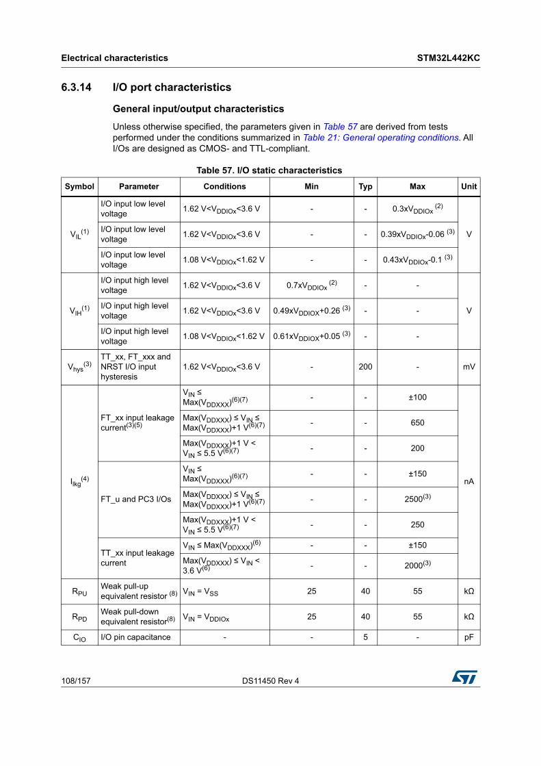
Electrical characteristics STM32L442KC
108/157 DS11450 Rev 4
6.3.14 I/O port characteristics
General input/output characteristics
Unless otherwise specified, the parameters given in Table 57 are derived from tests performed under the conditions summarized in Table 21: General operating conditions. All I/Os are designed as CMOS- and TTL-compliant.
Table 57. I/O static characteristics
Symbol Parameter Conditions Min Typ Max Unit
VIL(1)
I/O input low level voltage
1.62 V<VDDIOx<3.6 V - - 0.3xVDDIOx (2)
VI/O input low level voltage
1.62 V<VDDIOx<3.6 V - - 0.39xVDDIOx-0.06 (3)
I/O input low level voltage
1.08 V<VDDIOx<1.62 V - - 0.43xVDDIOx-0.1 (3)
VIH(1)
I/O input high level voltage
1.62 V<VDDIOx<3.6 V 0.7xVDDIOx (2) - -
VI/O input high level voltage
1.62 V<VDDIOx<3.6 V 0.49xVDDIOX+0.26 (3) - -
I/O input high level voltage
1.08 V<VDDIOx<1.62 V 0.61xVDDIOX+0.05 (3) - -
Vhys(3)
TT_xx, FT_xxx and NRST I/O input hysteresis
1.62 V<VDDIOx<3.6 V - 200 - mV
Ilkg(4)
FT_xx input leakage current(3)(5)
VIN ≤ Max(VDDXXX)(6)(7) - - ±100
nA
Max(VDDXXX) ≤ VIN ≤ Max(VDDXXX)+1 V(6)(7) - - 650
Max(VDDXXX)+1 V < VIN ≤ 5.5 V(6)(7) - - 200
FT_u and PC3 I/Os
VIN ≤ Max(VDDXXX)(6)(7) - - ±150
Max(VDDXXX) ≤ VIN ≤ Max(VDDXXX)+1 V(6)(7) - - 2500(3)
Max(VDDXXX)+1 V < VIN ≤ 5.5 V(6)(7) - - 250
TT_xx input leakage current
VIN ≤ Max(VDDXXX)(6) - - ±150
Max(VDDXXX) ≤ VIN < 3.6 V(6) - - 2000(3)
RPUWeak pull-up equivalent resistor (8) VIN = VSS 25 40 55 kΩ
RPDWeak pull-down equivalent resistor(8) VIN = VDDIOx 25 40 55 kΩ
CIO I/O pin capacitance - - 5 - pF
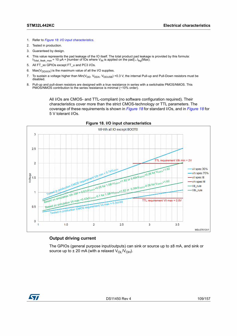
DS11450 Rev 4 109/157
STM32L442KC Electrical characteristics
149
All I/Os are CMOS- and TTL-compliant (no software configuration required). Their characteristics cover more than the strict CMOS-technology or TTL parameters. The coverage of these requirements is shown in Figure 18 for standard I/Os, and in Figure 18 for 5 V tolerant I/Os.
Figure 18. I/O input characteristics
Output driving current
The GPIOs (general purpose input/outputs) can sink or source up to ±8 mA, and sink or source up to ± 20 mA (with a relaxed VOL/VOH).
1. Refer to Figure 18: I/O input characteristics.
2. Tested in production.
3. Guaranteed by design.
4. This value represents the pad leakage of the IO itself. The total product pad leakage is provided by this formula: ITotal_Ileak_max = 10 µA + [number of IOs where VIN is applied on the pad] ₓ Ilkg(Max).
5. All FT_xx GPIOs except FT_u and PC3 I/Os.
6. Max(VDDXXX) is the maximum value of all the I/O supplies.
7. To sustain a voltage higher than Min(VDD, VDDA, VDDUSB) +0.3 V, the internal Pull-up and Pull-Down resistors must be disabled.
8. Pull-up and pull-down resistors are designed with a true resistance in series with a switchable PMOS/NMOS. This PMOS/NMOS contribution to the series resistance is minimal (~10% order).
MSv37613V1
Tested in production CMOS requirement Vih min = 0.7xVDDIOx
Based on simulation Vih min = 0.61xVDDIOx+0.05 for 1.08<VDDIOx<1.62 or 0.49xVDDIOx+0.26 for VDDIOx>1.62
Based on simulation Vil max =0.43xVDDIOx-0.1 for 1.08<VDDIOx<1.62 or 0.39xVDDIOx-0.06 for VDDIOx>1.62
Tested in production CMOS requirement Vil max = 0.3xVdd
TTL requirement Vih min = 2V
TTL requirement Vil max = 0.8V
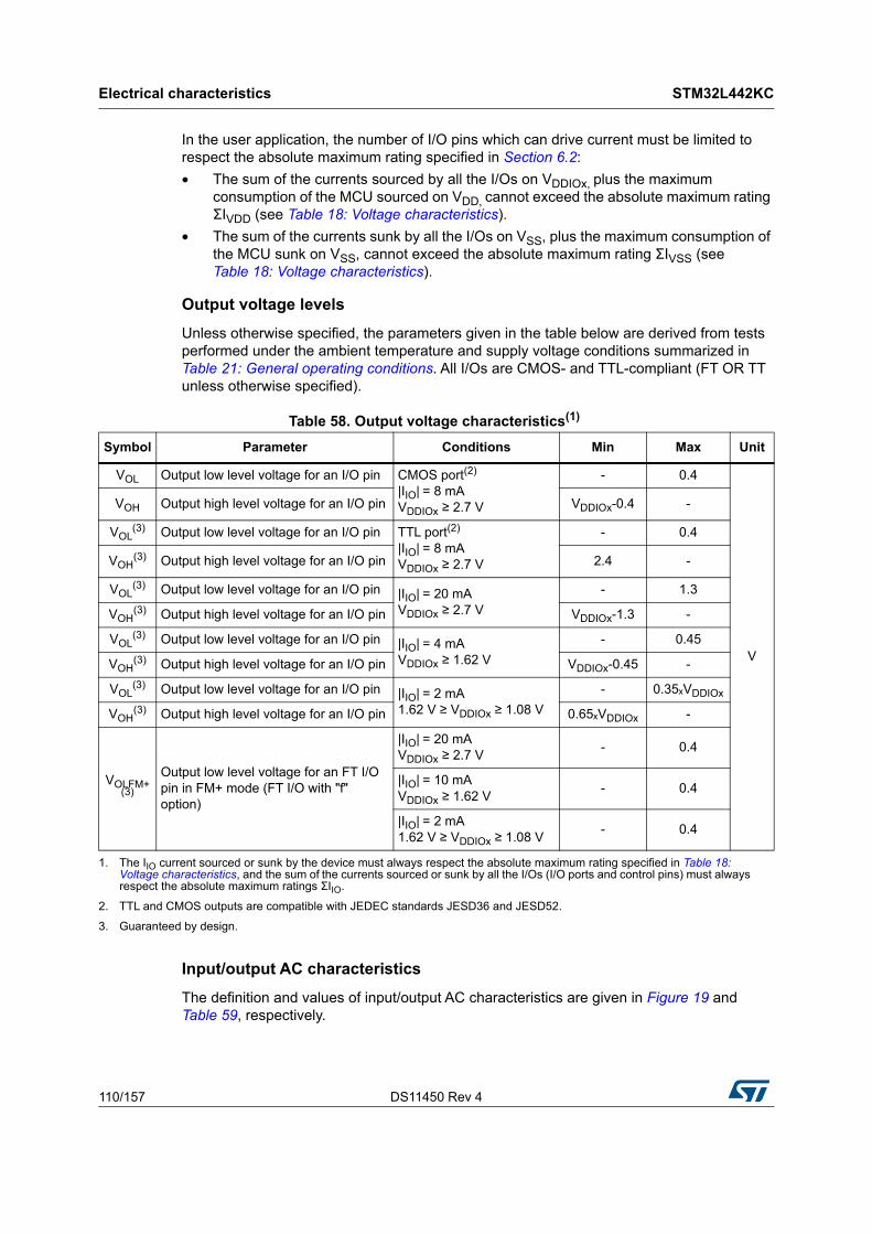
Electrical characteristics STM32L442KC
110/157 DS11450 Rev 4
In the user application, the number of I/O pins which can drive current must be limited to respect the absolute maximum rating specified in Section 6.2:
• The sum of the currents sourced by all the I/Os on VDDIOx, plus the maximum consumption of the MCU sourced on VDD, cannot exceed the absolute maximum rating ΣIVDD (see Table 18: Voltage characteristics).
• The sum of the currents sunk by all the I/Os on VSS, plus the maximum consumption of the MCU sunk on VSS, cannot exceed the absolute maximum rating ΣIVSS (see Table 18: Voltage characteristics).
Output voltage levels
Unless otherwise specified, the parameters given in the table below are derived from tests performed under the ambient temperature and supply voltage conditions summarized in Table 21: General operating conditions. All I/Os are CMOS- and TTL-compliant (FT OR TT unless otherwise specified).
Input/output AC characteristics
The definition and values of input/output AC characteristics are given in Figure 19 and Table 59, respectively.
Table 58. Output voltage characteristics(1)
Symbol Parameter Conditions Min Max Unit
VOL Output low level voltage for an I/O pin CMOS port(2) |IIO| = 8 mA VDDIOx ≥ 2.7 V
- 0.4
V
VOH Output high level voltage for an I/O pin VDDIOx-0.4 -
VOL(3) Output low level voltage for an I/O pin TTL port(2)
|IIO| = 8 mA VDDIOx ≥ 2.7 V
- 0.4
VOH(3) Output high level voltage for an I/O pin 2.4 -
VOL(3) Output low level voltage for an I/O pin |IIO| = 20 mA
VDDIOx ≥ 2.7 V
- 1.3
VOH(3) Output high level voltage for an I/O pin VDDIOx-1.3 -
VOL(3) Output low level voltage for an I/O pin |IIO| = 4 mA
VDDIOx ≥ 1.62 V
- 0.45
VOH(3) Output high level voltage for an I/O pin VDDIOx-0.45 -
VOL(3) Output low level voltage for an I/O pin |IIO| = 2 mA
1.62 V ≥ VDDIOx ≥ 1.08 V
- 0.35ₓVDDIOx
VOH(3) Output high level voltage for an I/O pin 0.65ₓVDDIOx -
VOLFM+(3)
Output low level voltage for an FT I/O pin in FM+ mode (FT I/O with "f" option)
|IIO| = 20 mA VDDIOx ≥ 2.7 V
- 0.4
|IIO| = 10 mA VDDIOx ≥ 1.62 V
- 0.4
|IIO| = 2 mA 1.62 V ≥ VDDIOx ≥ 1.08 V
- 0.4
1. The IIO current sourced or sunk by the device must always respect the absolute maximum rating specified in Table 18: Voltage characteristics, and the sum of the currents sourced or sunk by all the I/Os (I/O ports and control pins) must always respect the absolute maximum ratings ΣIIO.
2. TTL and CMOS outputs are compatible with JEDEC standards JESD36 and JESD52.
3. Guaranteed by design.
DS11450 Rev 4 111/157
STM32L442KC Electrical characteristics
149
Unless otherwise specified, the parameters given are derived from tests performed under the ambient temperature and supply voltage conditions summarized in Table 21: General operating conditions.
Table 59. I/O AC characteristics(1)(2)
Speed Symbol Parameter Conditions Min Max Unit
00
Fmax Maximum frequency
C=50 pF, 2.7 V≤VDDIOx≤3.6 V - 5
MHz
C=50 pF, 1.62 V≤VDDIOx≤2.7 V - 1
C=50 pF, 1.08 V≤VDDIOx≤1.62 V - 0.1
C=10 pF, 2.7 V≤VDDIOx≤3.6 V - 10
C=10 pF, 1.62 V≤VDDIOx≤2.7 V - 1.5
C=10 pF, 1.08 V≤VDDIOx≤1.62 V - 0.1
Tr/Tf Output rise and fall time
C=50 pF, 2.7 V≤VDDIOx≤3.6 V - 25
ns
C=50 pF, 1.62 V≤VDDIOx≤2.7 V - 52
C=50 pF, 1.08 V≤VDDIOx≤1.62 V - 140
C=10 pF, 2.7 V≤VDDIOx≤3.6 V - 17
C=10 pF, 1.62 V≤VDDIOx≤2.7 V - 37
C=10 pF, 1.08 V≤VDDIOx≤1.62 V - 110
01
Fmax Maximum frequency
C=50 pF, 2.7 V≤VDDIOx≤3.6 V - 25
MHz
C=50 pF, 1.62 V≤VDDIOx≤2.7 V - 10
C=50 pF, 1.08 V≤VDDIOx≤1.62 V - 1
C=10 pF, 2.7 V≤VDDIOx≤3.6 V - 50
C=10 pF, 1.62 V≤VDDIOx≤2.7 V - 15
C=10 pF, 1.08 V≤VDDIOx≤1.62 V - 1
Tr/Tf Output rise and fall time
C=50 pF, 2.7 V≤VDDIOx≤3.6 V - 9
ns
C=50 pF, 1.62 V≤VDDIOx≤2.7 V - 16
C=50 pF, 1.08 V≤VDDIOx≤1.62 V - 40
C=10 pF, 2.7 V≤VDDIOx≤3.6 V - 4.5
C=10 pF, 1.62 V≤VDDIOx≤2.7 V - 9
C=10 pF, 1.08 V≤VDDIOx≤1.62 V - 21
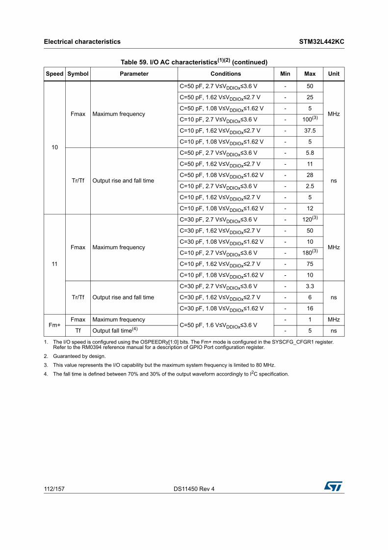
Electrical characteristics STM32L442KC
112/157 DS11450 Rev 4
10
Fmax Maximum frequency
C=50 pF, 2.7 V≤VDDIOx≤3.6 V - 50
MHz
C=50 pF, 1.62 V≤VDDIOx≤2.7 V - 25
C=50 pF, 1.08 V≤VDDIOx≤1.62 V - 5
C=10 pF, 2.7 V≤VDDIOx≤3.6 V - 100(3)
C=10 pF, 1.62 V≤VDDIOx≤2.7 V - 37.5
C=10 pF, 1.08 V≤VDDIOx≤1.62 V - 5
Tr/Tf Output rise and fall time
C=50 pF, 2.7 V≤VDDIOx≤3.6 V - 5.8
ns
C=50 pF, 1.62 V≤VDDIOx≤2.7 V - 11
C=50 pF, 1.08 V≤VDDIOx≤1.62 V - 28
C=10 pF, 2.7 V≤VDDIOx≤3.6 V - 2.5
C=10 pF, 1.62 V≤VDDIOx≤2.7 V - 5
C=10 pF, 1.08 V≤VDDIOx≤1.62 V - 12
11
Fmax Maximum frequency
C=30 pF, 2.7 V≤VDDIOx≤3.6 V - 120(3)
MHz
C=30 pF, 1.62 V≤VDDIOx≤2.7 V - 50
C=30 pF, 1.08 V≤VDDIOx≤1.62 V - 10
C=10 pF, 2.7 V≤VDDIOx≤3.6 V - 180(3)
C=10 pF, 1.62 V≤VDDIOx≤2.7 V - 75
C=10 pF, 1.08 V≤VDDIOx≤1.62 V - 10
Tr/Tf Output rise and fall time
C=30 pF, 2.7 V≤VDDIOx≤3.6 V - 3.3
nsC=30 pF, 1.62 V≤VDDIOx≤2.7 V - 6
C=30 pF, 1.08 V≤VDDIOx≤1.62 V - 16
Fm+Fmax Maximum frequency
C=50 pF, 1.6 V≤VDDIOx≤3.6 V- 1 MHz
Tf Output fall time(4) - 5 ns
1. The I/O speed is configured using the OSPEEDRy[1:0] bits. The Fm+ mode is configured in the SYSCFG_CFGR1 register. Refer to the RM0394 reference manual for a description of GPIO Port configuration register.
2. Guaranteed by design.
3. This value represents the I/O capability but the maximum system frequency is limited to 80 MHz.
4. The fall time is defined between 70% and 30% of the output waveform accordingly to I2C specification.
Table 59. I/O AC characteristics(1)(2) (continued)
Speed Symbol Parameter Conditions Min Max Unit
DS11450 Rev 4 113/157
STM32L442KC Electrical characteristics
149
Figure 19. I/O AC characteristics definition(1)
1. Refer to Table 59: I/O AC characteristics.
6.3.15 NRST pin characteristics
The NRST pin input driver uses the CMOS technology. It is connected to a permanent pull-up resistor, RPU.
Unless otherwise specified, the parameters given in the table below are derived from tests performed under the ambient temperature and supply voltage conditions summarized in Table 21: General operating conditions.
MS32132V2
T
10%
50%
90% 10%
50%
90%
Maximum frequency is achieved if (t + t (≤ 2/3)T and if the duty cycle is (45-55%)when loaded by the specified capacitance.
r f
r(IO)outt f(IO)outt
Table 60. NRST pin characteristics(1)
Symbol Parameter Conditions Min Typ Max Unit
VIL(NRST)NRST input low level voltage
- - - 0.3ₓVDDIOx
V
VIH(NRST)NRST input high level voltage
- 0.7ₓVDDIOx - -
Vhys(NRST)NRST Schmitt trigger voltage hysteresis
- - 200 - mV
RPUWeak pull-up equivalent resistor(2) VIN = VSS 25 40 55 kΩ
VF(NRST) NRST input filtered
pulse- - - 70 ns
VNF(NRST)NRST input not filtered pulse
1.71 V ≤ VDD ≤ 3.6 V 350 - - ns
1. Guaranteed by design.
2. The pull-up is designed with a true resistance in series with a switchable PMOS. This PMOS contribution to the series resistance is minimal (~10% order).
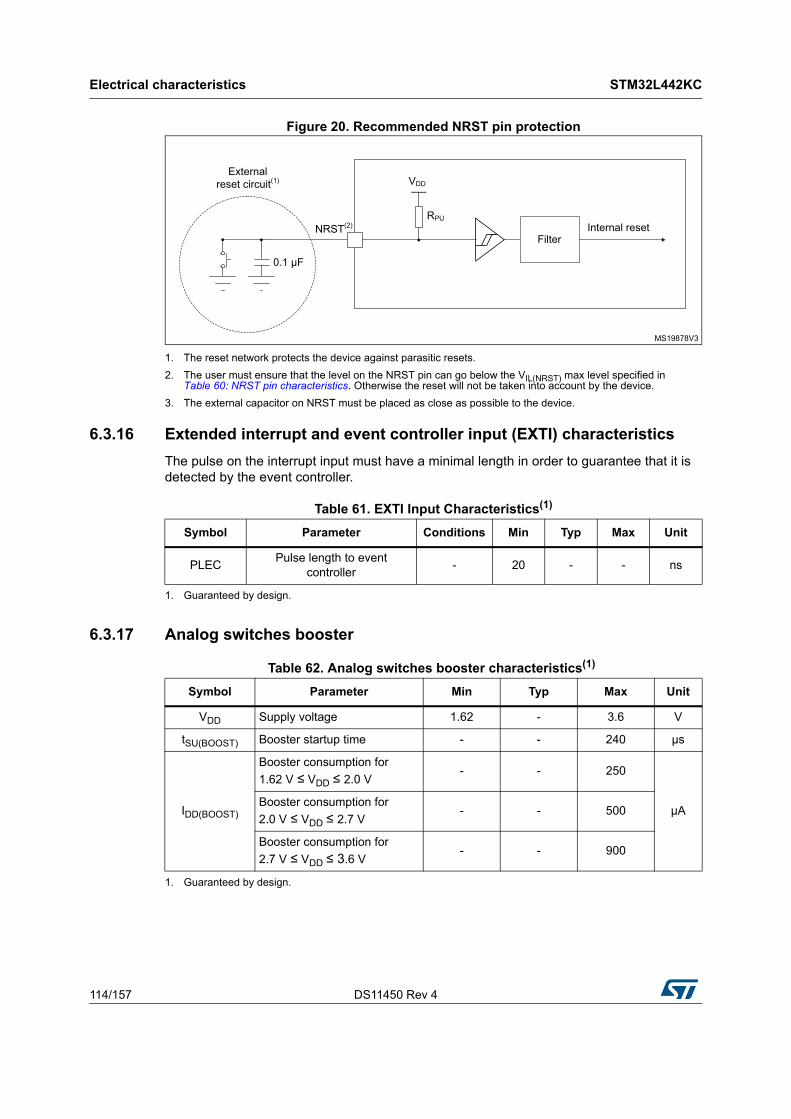
Electrical characteristics STM32L442KC
114/157 DS11450 Rev 4
Figure 20. Recommended NRST pin protection
1. The reset network protects the device against parasitic resets.
2. The user must ensure that the level on the NRST pin can go below the VIL(NRST) max level specified in Table 60: NRST pin characteristics. Otherwise the reset will not be taken into account by the device.
3. The external capacitor on NRST must be placed as close as possible to the device.
6.3.16 Extended interrupt and event controller input (EXTI) characteristics
The pulse on the interrupt input must have a minimal length in order to guarantee that it is detected by the event controller.
6.3.17 Analog switches booster
MS19878V3
RPU
VDD
Internal reset
Externalreset circuit(1)
NRST(2)
Filter
0.1 μF
Table 61. EXTI Input Characteristics(1)
1. Guaranteed by design.
Symbol Parameter Conditions Min Typ Max Unit
PLECPulse length to event
controller- 20 - - ns
Table 62. Analog switches booster characteristics(1)
1. Guaranteed by design.
Symbol Parameter Min Typ Max Unit
VDD Supply voltage 1.62 - 3.6 V
tSU(BOOST) Booster startup time - - 240 µs
IDD(BOOST)
Booster consumption for
1.62 V ≤ VDD ≤ 2.0 V- - 250
µABooster consumption for
2.0 V ≤ VDD ≤ 2.7 V- - 500
Booster consumption for
2.7 V ≤ VDD ≤ 3.6 V- - 900
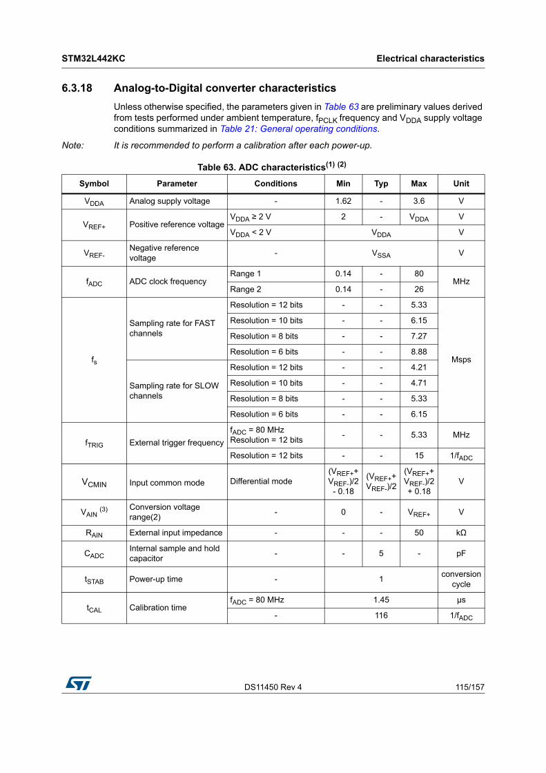
DS11450 Rev 4 115/157
STM32L442KC Electrical characteristics
149
6.3.18 Analog-to-Digital converter characteristics
Unless otherwise specified, the parameters given in Table 63 are preliminary values derived from tests performed under ambient temperature, fPCLK frequency and VDDA supply voltage conditions summarized in Table 21: General operating conditions.
Note: It is recommended to perform a calibration after each power-up.
Table 63. ADC characteristics(1) (2)
Symbol Parameter Conditions Min Typ Max Unit
VDDA Analog supply voltage - 1.62 - 3.6 V
VREF+ Positive reference voltageVDDA ≥ 2 V 2 - VDDA V
VDDA < 2 V VDDA V
VREF-Negative reference voltage
- VSSA V
fADC ADC clock frequencyRange 1 0.14 - 80
MHzRange 2 0.14 - 26
fs
Sampling rate for FAST channels
Resolution = 12 bits - - 5.33
Msps
Resolution = 10 bits - - 6.15
Resolution = 8 bits - - 7.27
Resolution = 6 bits - - 8.88
Sampling rate for SLOW channels
Resolution = 12 bits - - 4.21
Resolution = 10 bits - - 4.71
Resolution = 8 bits - - 5.33
Resolution = 6 bits - - 6.15
fTRIG External trigger frequency
fADC = 80 MHz Resolution = 12 bits
- - 5.33 MHz
Resolution = 12 bits - - 15 1/fADC
VCMIN Input common mode Differential mode(VREF++VREF-)/2
- 0.18
(VREF++VREF-)/2
(VREF++VREF-)/2 + 0.18
V
VAIN (3) Conversion voltage range(2)
- 0 - VREF+ V
RAIN External input impedance - - - 50 kΩ
CADCInternal sample and hold capacitor
- - 5 - pF
tSTAB Power-up time - 1conversion
cycle
tCAL Calibration timefADC = 80 MHz 1.45 µs
- 116 1/fADC
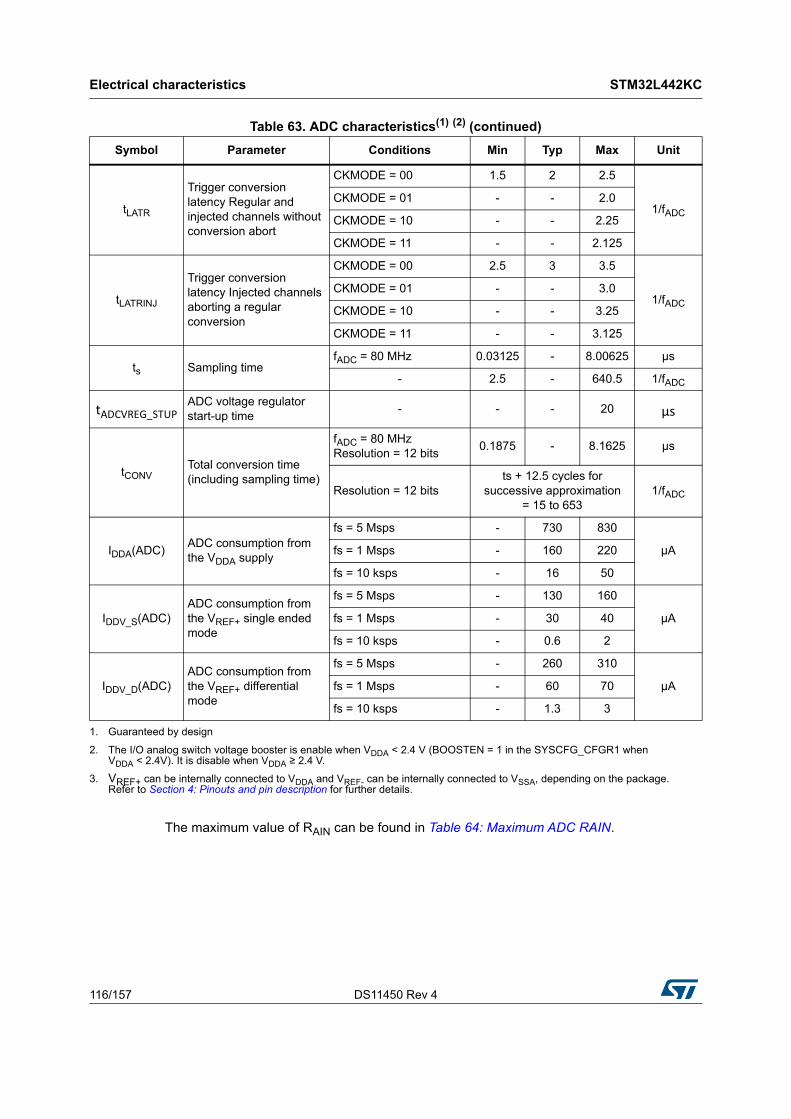
Electrical characteristics STM32L442KC
116/157 DS11450 Rev 4
The maximum value of RAIN can be found in Table 64: Maximum ADC RAIN.
tLATR
Trigger conversion latency Regular and injected channels without conversion abort
CKMODE = 00 1.5 2 2.5
1/fADC
CKMODE = 01 - - 2.0
CKMODE = 10 - - 2.25
CKMODE = 11 - - 2.125
tLATRINJ
Trigger conversion latency Injected channels aborting a regular conversion
CKMODE = 00 2.5 3 3.5
1/fADC
CKMODE = 01 - - 3.0
CKMODE = 10 - - 3.25
CKMODE = 11 - - 3.125
ts Sampling timefADC = 80 MHz 0.03125 - 8.00625 µs
- 2.5 - 640.5 1/fADC
tADCVREG_STUPADC voltage regulator start-up time
- - - 20 µs
tCONVTotal conversion time (including sampling time)
fADC = 80 MHz Resolution = 12 bits
0.1875 - 8.1625 µs
Resolution = 12 bitsts + 12.5 cycles for
successive approximation= 15 to 653
1/fADC
IDDA(ADC)ADC consumption from the VDDA supply
fs = 5 Msps - 730 830
µAfs = 1 Msps - 160 220
fs = 10 ksps - 16 50
IDDV_S(ADC)ADC consumption from the VREF+ single ended mode
fs = 5 Msps - 130 160
µAfs = 1 Msps - 30 40
fs = 10 ksps - 0.6 2
IDDV_D(ADC)ADC consumption from the VREF+ differential mode
fs = 5 Msps - 260 310
µAfs = 1 Msps - 60 70
fs = 10 ksps - 1.3 3
1. Guaranteed by design
2. The I/O analog switch voltage booster is enable when VDDA < 2.4 V (BOOSTEN = 1 in the SYSCFG_CFGR1 when VDDA < 2.4V). It is disable when VDDA ≥ 2.4 V.
3. VREF+ can be internally connected to VDDA and VREF- can be internally connected to VSSA, depending on the package. Refer to Section 4: Pinouts and pin description for further details.
Table 63. ADC characteristics(1) (2) (continued)
Symbol Parameter Conditions Min Typ Max Unit
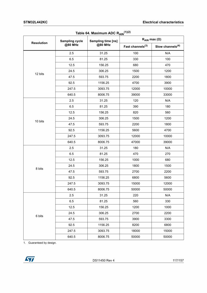
DS11450 Rev 4 117/157
STM32L442KC Electrical characteristics
149
Table 64. Maximum ADC RAIN(1)(2)
ResolutionSampling cycle
@80 MHzSampling time [ns]
@80 MHz
RAIN max (Ω)
Fast channels(3) Slow channels(4)
12 bits
2.5 31.25 100 N/A
6.5 81.25 330 100
12.5 156.25 680 470
24.5 306.25 1500 1200
47.5 593.75 2200 1800
92.5 1156.25 4700 3900
247.5 3093.75 12000 10000
640.5 8006.75 39000 33000
10 bits
2.5 31.25 120 N/A
6.5 81.25 390 180
12.5 156.25 820 560
24.5 306.25 1500 1200
47.5 593.75 2200 1800
92.5 1156.25 5600 4700
247.5 3093.75 12000 10000
640.5 8006.75 47000 39000
8 bits
2.5 31.25 180 N/A
6.5 81.25 470 270
12.5 156.25 1000 680
24.5 306.25 1800 1500
47.5 593.75 2700 2200
92.5 1156.25 6800 5600
247.5 3093.75 15000 12000
640.5 8006.75 50000 50000
6 bits
2.5 31.25 220 N/A
6.5 81.25 560 330
12.5 156.25 1200 1000
24.5 306.25 2700 2200
47.5 593.75 3900 3300
92.5 1156.25 8200 6800
247.5 3093.75 18000 15000
640.5 8006.75 50000 50000
1. Guaranteed by design.
Electrical characteristics STM32L442KC
118/157 DS11450 Rev 4
2. The I/O analog switch voltage booster is enable when VDDA < 2.4 V (BOOSTEN = 1 in the SYSCFG_CFGR1 when VDDA < 2.4V). It is disable when VDDA ≥ 2.4 V.
3. Fast channels are: PC0, PC1, PC2, PC3, PA0, PA1.
4. Slow channels are: all ADC inputs except the fast channels.
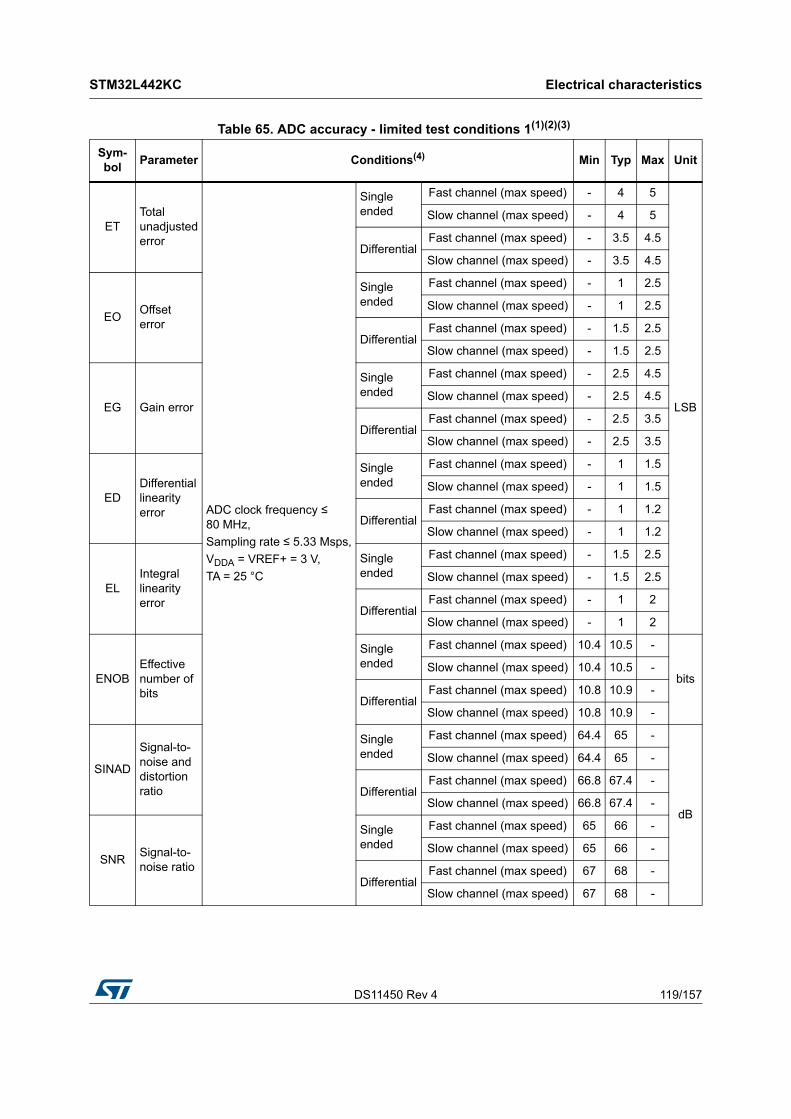
DS11450 Rev 4 119/157
STM32L442KC Electrical characteristics
149
Table 65. ADC accuracy - limited test conditions 1(1)(2)(3)
Sym-bol
Parameter Conditions(4) Min Typ Max Unit
ETTotal unadjusted error
ADC clock frequency ≤ 80 MHz,
Sampling rate ≤ 5.33 Msps,
VDDA = VREF+ = 3 V,
TA = 25 °C
Single ended
Fast channel (max speed) - 4 5
LSB
Slow channel (max speed) - 4 5
DifferentialFast channel (max speed) - 3.5 4.5
Slow channel (max speed) - 3.5 4.5
EOOffset error
Single ended
Fast channel (max speed) - 1 2.5
Slow channel (max speed) - 1 2.5
DifferentialFast channel (max speed) - 1.5 2.5
Slow channel (max speed) - 1.5 2.5
EG Gain error
Single ended
Fast channel (max speed) - 2.5 4.5
Slow channel (max speed) - 2.5 4.5
DifferentialFast channel (max speed) - 2.5 3.5
Slow channel (max speed) - 2.5 3.5
EDDifferential linearity error
Single ended
Fast channel (max speed) - 1 1.5
Slow channel (max speed) - 1 1.5
DifferentialFast channel (max speed) - 1 1.2
Slow channel (max speed) - 1 1.2
ELIntegral linearity error
Single ended
Fast channel (max speed) - 1.5 2.5
Slow channel (max speed) - 1.5 2.5
DifferentialFast channel (max speed) - 1 2
Slow channel (max speed) - 1 2
ENOBEffective number of bits
Single ended
Fast channel (max speed) 10.4 10.5 -
bitsSlow channel (max speed) 10.4 10.5 -
DifferentialFast channel (max speed) 10.8 10.9 -
Slow channel (max speed) 10.8 10.9 -
SINAD
Signal-to-noise and distortion ratio
Single ended
Fast channel (max speed) 64.4 65 -
dB
Slow channel (max speed) 64.4 65 -
DifferentialFast channel (max speed) 66.8 67.4 -
Slow channel (max speed) 66.8 67.4 -
SNRSignal-to-noise ratio
Single ended
Fast channel (max speed) 65 66 -
Slow channel (max speed) 65 66 -
DifferentialFast channel (max speed) 67 68 -
Slow channel (max speed) 67 68 -

Electrical characteristics STM32L442KC
120/157 DS11450 Rev 4
THDTotal harmonic distortion
ADC clock frequency ≤ 80 MHz,
Sampling rate ≤ 5.33 Msps,
VDDA = VREF+ = 3 V,
TA = 25 °C
Single ended
Fast channel (max speed) - -74 -73
dBSlow channel (max speed) - -74 -73
DifferentialFast channel (max speed) - -79 -76
Slow channel (max speed) - -79 -76
1. Guaranteed by design.
2. ADC DC accuracy values are measured after internal calibration.
3. ADC accuracy vs. negative Injection Current: Injecting negative current on any analog input pins should be avoided as this significantly reduces the accuracy of the conversion being performed on another analog input. It is recommended to add a Schottky diode (pin to ground) to analog pins which may potentially inject negative current.
4. The I/O analog switch voltage booster is enable when VDDA < 2.4 V (BOOSTEN = 1 in the SYSCFG_CFGR1 when VDDA < 2.4 V). It is disable when VDDA ≥ 2.4 V. No oversampling.
Table 65. ADC accuracy - limited test conditions 1(1)(2)(3) (continued)
Sym-bol
Parameter Conditions(4) Min Typ Max Unit

DS11450 Rev 4 121/157
STM32L442KC Electrical characteristics
149
Table 66. ADC accuracy - limited test conditions 2(1)(2)(3)
Sym-bol
Parameter Conditions(4) Min Typ Max Unit
ETTotal unadjusted error
ADC clock frequency ≤ 80 MHz,
Sampling rate ≤ 5.33 Msps,
2 V ≤ VDDA
Single ended
Fast channel (max speed) - 4 6.5
LSB
Slow channel (max speed) - 4 6.5
DifferentialFast channel (max speed) - 3.5 5.5
Slow channel (max speed) - 3.5 5.5
EOOffset error
Single ended
Fast channel (max speed) - 1 4.5
Slow channel (max speed) - 1 5
DifferentialFast channel (max speed) - 1.5 3
Slow channel (max speed) - 1.5 3
EG Gain error
Single ended
Fast channel (max speed) - 2.5 6
Slow channel (max speed) - 2.5 6
DifferentialFast channel (max speed) - 2.5 3.5
Slow channel (max speed) - 2.5 3.5
EDDifferential linearity error
Single ended
Fast channel (max speed) - 1 1.5
Slow channel (max speed) - 1 1.5
DifferentialFast channel (max speed) - 1 1.2
Slow channel (max speed) - 1 1.2
ELIntegral linearity error
Single ended
Fast channel (max speed) - 1.5 3.5
Slow channel (max speed) - 1.5 3.5
DifferentialFast channel (max speed) - 1 3
Slow channel (max speed) - 1 2.5
ENOBEffective number of bits
Single ended
Fast channel (max speed) 10 10.5 -
bitsSlow channel (max speed) 10 10.5 -
DifferentialFast channel (max speed) 10.7 10.9 -
Slow channel (max speed) 10.7 10.9 -
SINAD
Signal-to-noise and distortion ratio
Single ended
Fast channel (max speed) 62 65 -
dB
Slow channel (max speed) 62 65 -
DifferentialFast channel (max speed) 66 67.4 -
Slow channel (max speed) 66 67.4 -
SNRSignal-to-noise ratio
Single ended
Fast channel (max speed) 64 66 -
Slow channel (max speed) 64 66 -
DifferentialFast channel (max speed) 66.5 68 -
Slow channel (max speed) 66.5 68 -
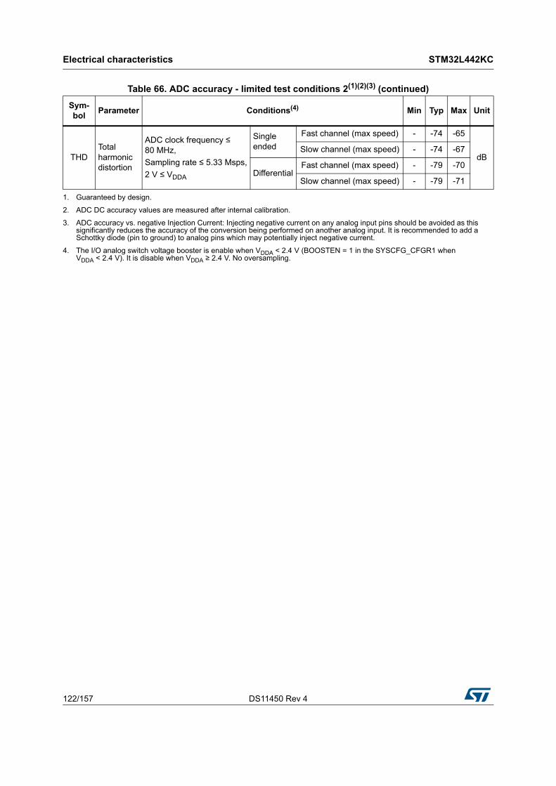
Electrical characteristics STM32L442KC
122/157 DS11450 Rev 4
THDTotal harmonic distortion
ADC clock frequency ≤ 80 MHz,
Sampling rate ≤ 5.33 Msps,
2 V ≤ VDDA
Single ended
Fast channel (max speed) - -74 -65
dBSlow channel (max speed) - -74 -67
DifferentialFast channel (max speed) - -79 -70
Slow channel (max speed) - -79 -71
1. Guaranteed by design.
2. ADC DC accuracy values are measured after internal calibration.
3. ADC accuracy vs. negative Injection Current: Injecting negative current on any analog input pins should be avoided as this significantly reduces the accuracy of the conversion being performed on another analog input. It is recommended to add a Schottky diode (pin to ground) to analog pins which may potentially inject negative current.
4. The I/O analog switch voltage booster is enable when VDDA < 2.4 V (BOOSTEN = 1 in the SYSCFG_CFGR1 when VDDA < 2.4 V). It is disable when VDDA ≥ 2.4 V. No oversampling.
Table 66. ADC accuracy - limited test conditions 2(1)(2)(3) (continued)
Sym-bol
Parameter Conditions(4) Min Typ Max Unit
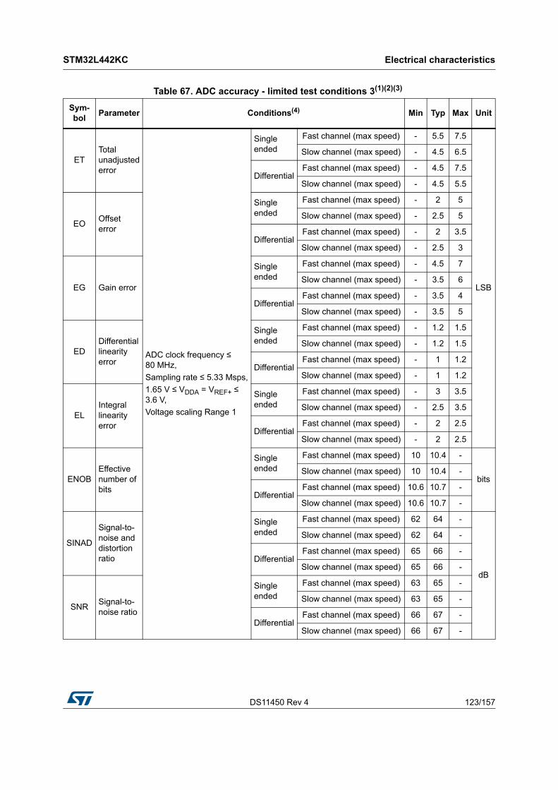
DS11450 Rev 4 123/157
STM32L442KC Electrical characteristics
149
Table 67. ADC accuracy - limited test conditions 3(1)(2)(3)
Sym-bol
Parameter Conditions(4) Min Typ Max Unit
ETTotal unadjusted error
ADC clock frequency ≤ 80 MHz,
Sampling rate ≤ 5.33 Msps,
1.65 V ≤ VDDA = VREF+ ≤ 3.6 V,
Voltage scaling Range 1
Single ended
Fast channel (max speed) - 5.5 7.5
LSB
Slow channel (max speed) - 4.5 6.5
DifferentialFast channel (max speed) - 4.5 7.5
Slow channel (max speed) - 4.5 5.5
EOOffset error
Single ended
Fast channel (max speed) - 2 5
Slow channel (max speed) - 2.5 5
DifferentialFast channel (max speed) - 2 3.5
Slow channel (max speed) - 2.5 3
EG Gain error
Single ended
Fast channel (max speed) - 4.5 7
Slow channel (max speed) - 3.5 6
DifferentialFast channel (max speed) - 3.5 4
Slow channel (max speed) - 3.5 5
EDDifferential linearity error
Single ended
Fast channel (max speed) - 1.2 1.5
Slow channel (max speed) - 1.2 1.5
DifferentialFast channel (max speed) - 1 1.2
Slow channel (max speed) - 1 1.2
ELIntegral linearity error
Single ended
Fast channel (max speed) - 3 3.5
Slow channel (max speed) - 2.5 3.5
DifferentialFast channel (max speed) - 2 2.5
Slow channel (max speed) - 2 2.5
ENOBEffective number of bits
Single ended
Fast channel (max speed) 10 10.4 -
bitsSlow channel (max speed) 10 10.4 -
DifferentialFast channel (max speed) 10.6 10.7 -
Slow channel (max speed) 10.6 10.7 -
SINAD
Signal-to-noise and distortion ratio
Single ended
Fast channel (max speed) 62 64 -
dB
Slow channel (max speed) 62 64 -
DifferentialFast channel (max speed) 65 66 -
Slow channel (max speed) 65 66 -
SNRSignal-to-noise ratio
Single ended
Fast channel (max speed) 63 65 -
Slow channel (max speed) 63 65 -
DifferentialFast channel (max speed) 66 67 -
Slow channel (max speed) 66 67 -
Electrical characteristics STM32L442KC
124/157 DS11450 Rev 4
THDTotal harmonic distortion
ADC clock frequency ≤ 80 MHz,
Sampling rate ≤ 5.33 Msps,
1.65 V ≤ VDDA = VREF+ ≤ 3.6 V,
Voltage scaling Range 1
Single ended
Fast channel (max speed) - -69 -67
dB
Slow channel (max speed) - -71 -67
Differential
Fast channel (max speed) - -72 -71
Slow channel (max speed) - -72 -71
1. Guaranteed by design.
2. ADC DC accuracy values are measured after internal calibration.
3. ADC accuracy vs. negative Injection Current: Injecting negative current on any analog input pins should be avoided as this significantly reduces the accuracy of the conversion being performed on another analog input. It is recommended to add a Schottky diode (pin to ground) to analog pins which may potentially inject negative current.
4. The I/O analog switch voltage booster is enable when VDDA < 2.4 V (BOOSTEN = 1 in the SYSCFG_CFGR1 when VDDA < 2.4 V). It is disable when VDDA ≥ 2.4 V. No oversampling.
Table 67. ADC accuracy - limited test conditions 3(1)(2)(3) (continued)
Sym-bol
Parameter Conditions(4) Min Typ Max Unit
DS11450 Rev 4 125/157
STM32L442KC Electrical characteristics
149
Table 68. ADC accuracy - limited test conditions 4(1)(2)(3)
Sym-bol
Parameter Conditions(4) Min Typ Max Unit
ETTotal unadjusted error
ADC clock frequency ≤ 26 MHz,
1.65 V ≤ VDDA = VREF+ ≤ 3.6 V,
Voltage scaling Range 2
Single ended
Fast channel (max speed) - 5 5.4
LSB
Slow channel (max speed) - 4 5
DifferentialFast channel (max speed) - 4 5
Slow channel (max speed) - 3.5 4.5
EOOffset error
Single ended
Fast channel (max speed) - 2 4
Slow channel (max speed) - 2 4
DifferentialFast channel (max speed) - 2 3.5
Slow channel (max speed) - 2 3.5
EG Gain error
Single ended
Fast channel (max speed) - 4 4.5
Slow channel (max speed) - 4 4.5
DifferentialFast channel (max speed) - 3 4
Slow channel (max speed) - 3 4
EDDifferential linearity error
Single ended
Fast channel (max speed) - 1 1.5
Slow channel (max speed) - 1 1.5
DifferentialFast channel (max speed) - 1 1.2
Slow channel (max speed) - 1 1.2
ELIntegral linearity error
Single ended
Fast channel (max speed) - 2.5 3
Slow channel (max speed) - 2.5 3
DifferentialFast channel (max speed) - 2 2.5
Slow channel (max speed) - 2 2.5
ENOBEffective number of bits
Single ended
Fast channel (max speed) 10.2 10.5 -
bitsSlow channel (max speed) 10.2 10.5 -
DifferentialFast channel (max speed) 10.6 10.7 -
Slow channel (max speed) 10.6 10.7 -
SINAD
Signal-to-noise and distortion ratio
Single ended
Fast channel (max speed) 63 65 -
dB
Slow channel (max speed) 63 65 -
DifferentialFast channel (max speed) 65 66 -
Slow channel (max speed) 65 66 -
SNRSignal-to-noise ratio
Single ended
Fast channel (max speed) 64 65 -
Slow channel (max speed) 64 65 -
DifferentialFast channel (max speed) 66 67 -
Slow channel (max speed) 66 67 -
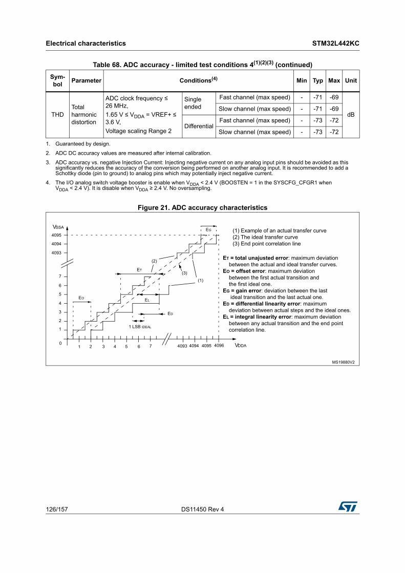
Electrical characteristics STM32L442KC
126/157 DS11450 Rev 4
Figure 21. ADC accuracy characteristics
THDTotal harmonic distortion
ADC clock frequency ≤ 26 MHz,
1.65 V ≤ VDDA = VREF+ ≤ 3.6 V,
Voltage scaling Range 2
Single ended
Fast channel (max speed) - -71 -69
dBSlow channel (max speed) - -71 -69
DifferentialFast channel (max speed) - -73 -72
Slow channel (max speed) - -73 -72
1. Guaranteed by design.
2. ADC DC accuracy values are measured after internal calibration.
3. ADC accuracy vs. negative Injection Current: Injecting negative current on any analog input pins should be avoided as this significantly reduces the accuracy of the conversion being performed on another analog input. It is recommended to add a Schottky diode (pin to ground) to analog pins which may potentially inject negative current.
4. The I/O analog switch voltage booster is enable when VDDA < 2.4 V (BOOSTEN = 1 in the SYSCFG_CFGR1 when VDDA < 2.4 V). It is disable when VDDA ≥ 2.4 V. No oversampling.
Table 68. ADC accuracy - limited test conditions 4(1)(2)(3) (continued)
Sym-bol
Parameter Conditions(4) Min Typ Max Unit
ET = total unajusted error: maximum deviation between the actual and ideal transfer curves.EO = offset error: maximum deviation between the first actual transition and the first ideal one.EG = gain error: deviation between the last ideal transition and the last actual one.ED = differential linearity error: maximum deviation between actual steps and the ideal ones.EL = integral linearity error: maximum deviation between any actual transition and the end point correlation line.
(1) Example of an actual transfer curve(2) The ideal transfer curve(3) End point correlation line
4095
4094
4093
7
6
5
4
3
2
1
02 3 4 5 61 7 4093 4094 4095 4096 VDDA
VSSA
EO
ET
EL
EG
ED
1 LSB IDEAL
(1)
(3)
(2)
MS19880V2
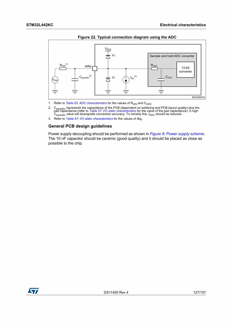
DS11450 Rev 4 127/157
STM32L442KC Electrical characteristics
149
Figure 22. Typical connection diagram using the ADC
1. Refer to Table 63: ADC characteristics for the values of RAIN and CADC.
2. Cparasitic represents the capacitance of the PCB (dependent on soldering and PCB layout quality) plus the pad capacitance (refer to Table 57: I/O static characteristics for the value of the pad capacitance). A high Cparasitic value will downgrade conversion accuracy. To remedy this, fADC should be reduced.
3. Refer to Table 57: I/O static characteristics for the values of Ilkg.
General PCB design guidelines
Power supply decoupling should be performed as shown in Figure 9: Power supply scheme. The 10 nF capacitor should be ceramic (good quality) and it should be placed as close as possible to the chip.
MS33900V5
Sample and hold ADC converter
12-bit converter
Cparasitic(2) Ilkg
(3) VT CADC
VDDA
RAIN(1)
VAIN
VT
AINx RADC
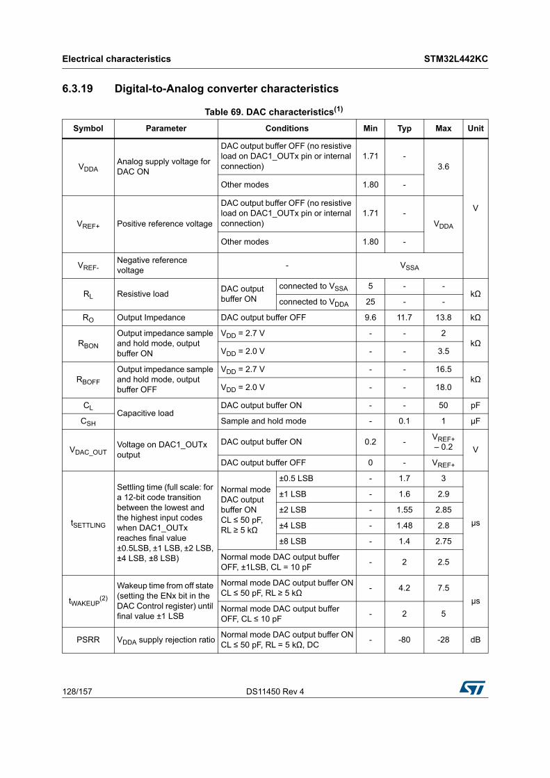
Electrical characteristics STM32L442KC
128/157 DS11450 Rev 4
6.3.19 Digital-to-Analog converter characteristics
Table 69. DAC characteristics(1)
Symbol Parameter Conditions Min Typ Max Unit
VDDAAnalog supply voltage for DAC ON
DAC output buffer OFF (no resistive load on DAC1_OUTx pin or internal connection)
1.71 -3.6
V
Other modes 1.80 -
VREF+ Positive reference voltage
DAC output buffer OFF (no resistive load on DAC1_OUTx pin or internal connection)
1.71 -VDDA
Other modes 1.80 -
VREF-Negative reference voltage
- VSSA
RL Resistive loadDAC output buffer ON
connected to VSSA 5 - -kΩ
connected to VDDA 25 - -
RO Output Impedance DAC output buffer OFF 9.6 11.7 13.8 kΩ
RBON
Output impedance sample and hold mode, output buffer ON
VDD = 2.7 V - - 2kΩ
VDD = 2.0 V - - 3.5
RBOFF
Output impedance sample and hold mode, output buffer OFF
VDD = 2.7 V - - 16.5kΩ
VDD = 2.0 V - - 18.0
CLCapacitive load
DAC output buffer ON - - 50 pF
CSH Sample and hold mode - 0.1 1 µF
VDAC_OUTVoltage on DAC1_OUTx output
DAC output buffer ON 0.2 -VREF+ – 0.2 V
DAC output buffer OFF 0 - VREF+
tSETTLING
Settling time (full scale: for a 12-bit code transition between the lowest and the highest input codes when DAC1_OUTx reaches final value ±0.5LSB, ±1 LSB, ±2 LSB, ±4 LSB, ±8 LSB)
Normal mode DAC output buffer ON CL ≤ 50 pF, RL ≥ 5 kΩ
±0.5 LSB - 1.7 3
µs
±1 LSB - 1.6 2.9
±2 LSB - 1.55 2.85
±4 LSB - 1.48 2.8
±8 LSB - 1.4 2.75
Normal mode DAC output buffer OFF, ±1LSB, CL = 10 pF
- 2 2.5
tWAKEUP(2)
Wakeup time from off state (setting the ENx bit in the DAC Control register) until final value ±1 LSB
Normal mode DAC output buffer ON CL ≤ 50 pF, RL ≥ 5 kΩ
- 4.2 7.5
µsNormal mode DAC output buffer OFF, CL ≤ 10 pF
- 2 5
PSRR VDDA supply rejection ratioNormal mode DAC output buffer ON CL ≤ 50 pF, RL = 5 kΩ, DC
- -80 -28 dB
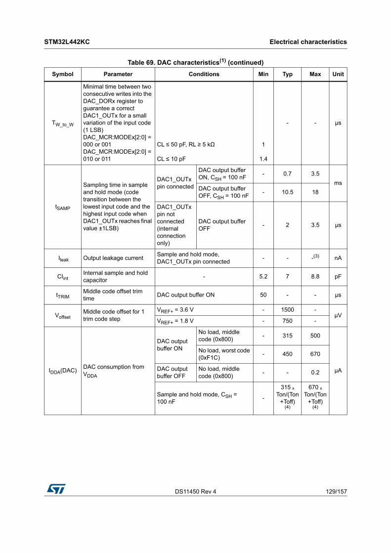
DS11450 Rev 4 129/157
STM32L442KC Electrical characteristics
149
TW_to_W
Minimal time between two consecutive writes into the DAC_DORx register to guarantee a correct DAC1_OUTx for a small variation of the input code (1 LSB) DAC_MCR:MODEx[2:0] = 000 or 001 DAC_MCR:MODEx[2:0] = 010 or 011
CL ≤ 50 pF, RL ≥ 5 kΩ CL ≤ 10 pF
1
1.4
- - µs
tSAMP
Sampling time in sample and hold mode (code transition between the lowest input code and the highest input code when DAC1_OUTx reaches final value ±1LSB)
DAC1_OUTx pin connected
DAC output buffer ON, CSH = 100 nF
- 0.7 3.5
msDAC output buffer OFF, CSH = 100 nF
- 10.5 18
DAC1_OUTx pin not connected (internal connection only)
DAC output buffer OFF
- 2 3.5 µs
Ileak Output leakage currentSample and hold mode, DAC1_OUTx pin connected
- - -(3) nA
CIintInternal sample and hold capacitor
- 5.2 7 8.8 pF
tTRIMMiddle code offset trim time
DAC output buffer ON 50 - - µs
VoffsetMiddle code offset for 1 trim code step
VREF+ = 3.6 V - 1500 -µV
VREF+ = 1.8 V - 750 -
IDDA(DAC)DAC consumption from VDDA
DAC output buffer ON
No load, middle code (0x800)
- 315 500
µA
No load, worst code (0xF1C)
- 450 670
DAC output buffer OFF
No load, middle code (0x800)
- - 0.2
Sample and hold mode, CSH = 100 nF
-
315 ₓ Ton/(Ton
+Toff)(4)
670 ₓTon/(Ton
+Toff)(4)
Table 69. DAC characteristics(1) (continued)
Symbol Parameter Conditions Min Typ Max Unit
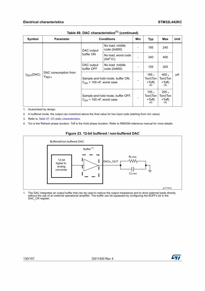
Electrical characteristics STM32L442KC
130/157 DS11450 Rev 4
Figure 23. 12-bit buffered / non-buffered DAC
1. The DAC integrates an output buffer that can be used to reduce the output impedance and to drive external loads directly without the use of an external operational amplifier. The buffer can be bypassed by configuring the BOFFx bit in the DAC_CR register.
IDDV(DAC)DAC consumption from VREF+
DAC output buffer ON
No load, middle code (0x800)
- 185 240
µA
No load, worst code (0xF1C)
- 340 400
DAC output buffer OFF
No load, middle code (0x800)
- 155 205
Sample and hold mode, buffer ON, CSH = 100 nF, worst case
-
185 ₓTon/(Ton
+Toff)(4)
400 ₓTon/(Ton
+Toff)(4)
Sample and hold mode, buffer OFF, CSH = 100 nF, worst case
-
155 ₓTon/(Ton
+Toff)(4)
205 ₓTon/(Ton
+Toff)(4)
1. Guaranteed by design.
2. In buffered mode, the output can overshoot above the final value for low input code (starting from min value).
3. Refer to Table 57: I/O static characteristics.
4. Ton is the Refresh phase duration. Toff is the Hold phase duration. Refer to RM0394 reference manual for more details.
Table 69. DAC characteristics(1) (continued)
Symbol Parameter Conditions Min Typ Max Unit
(1)Buffer
12-bitdigital to analog
converter
Buffered/non-buffered DAC
DACx_OUT
RLOAD
CLOAD
ai17157d
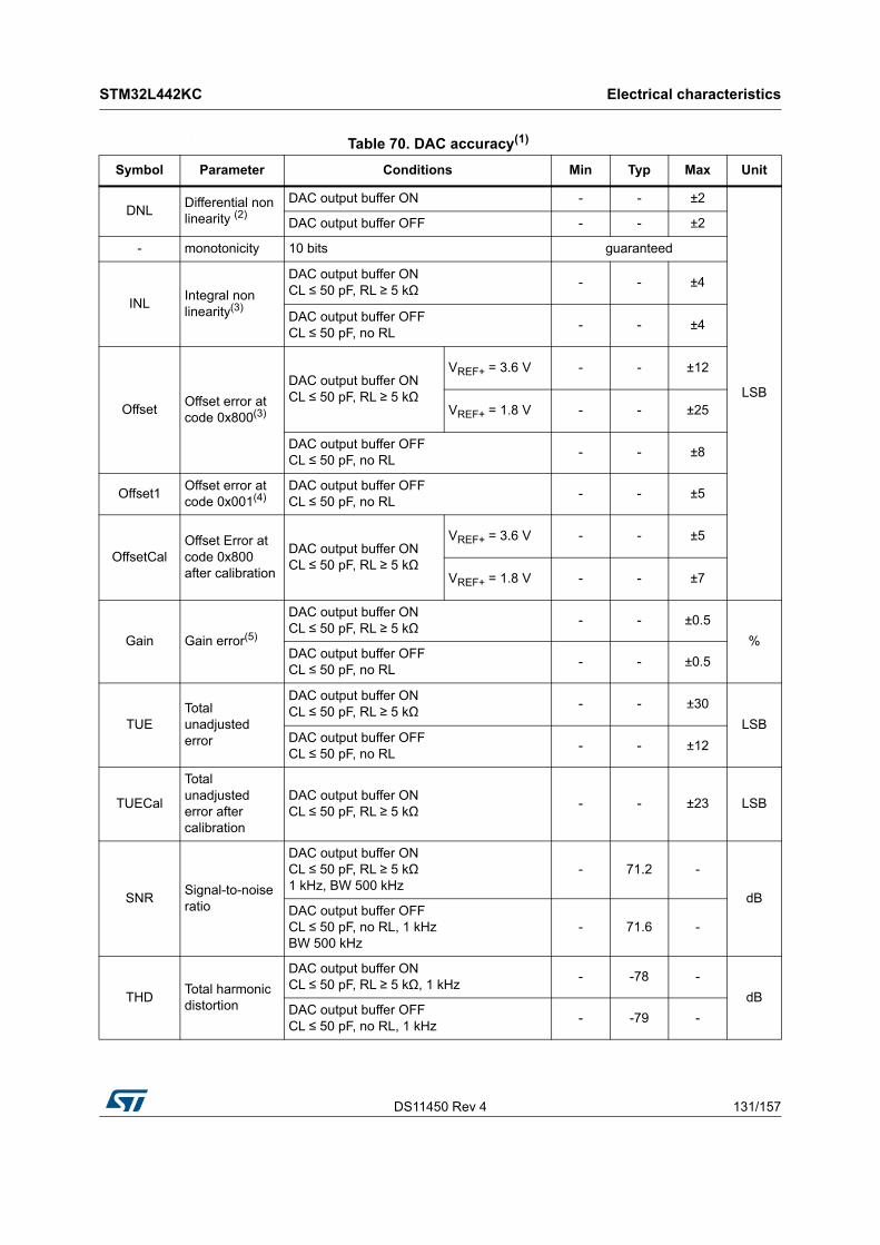
DS11450 Rev 4 131/157
STM32L442KC Electrical characteristics
149
.
Table 70. DAC accuracy(1)
Symbol Parameter Conditions Min Typ Max Unit
DNLDifferential non linearity (2)
DAC output buffer ON - - ±2
LSB
DAC output buffer OFF - - ±2
- monotonicity 10 bits guaranteed
INLIntegral non linearity(3)
DAC output buffer ON CL ≤ 50 pF, RL ≥ 5 kΩ
- - ±4
DAC output buffer OFF CL ≤ 50 pF, no RL
- - ±4
OffsetOffset error at code 0x800(3)
DAC output buffer ON CL ≤ 50 pF, RL ≥ 5 kΩ
VREF+ = 3.6 V - - ±12
VREF+ = 1.8 V - - ±25
DAC output buffer OFF CL ≤ 50 pF, no RL
- - ±8
Offset1Offset error at code 0x001(4)
DAC output buffer OFF CL ≤ 50 pF, no RL
- - ±5
OffsetCalOffset Error at code 0x800 after calibration
DAC output buffer ON CL ≤ 50 pF, RL ≥ 5 kΩ
VREF+ = 3.6 V - - ±5
VREF+ = 1.8 V - - ±7
Gain Gain error(5)
DAC output buffer ON CL ≤ 50 pF, RL ≥ 5 kΩ
- - ±0.5
%DAC output buffer OFF CL ≤ 50 pF, no RL
- - ±0.5
TUETotal unadjusted error
DAC output buffer ON CL ≤ 50 pF, RL ≥ 5 kΩ
- - ±30
LSBDAC output buffer OFF CL ≤ 50 pF, no RL
- - ±12
TUECal
Total unadjusted error after calibration
DAC output buffer ON CL ≤ 50 pF, RL ≥ 5 kΩ
- - ±23 LSB
SNRSignal-to-noise ratio
DAC output buffer ON CL ≤ 50 pF, RL ≥ 5 kΩ 1 kHz, BW 500 kHz
- 71.2 -
dBDAC output buffer OFF CL ≤ 50 pF, no RL, 1 kHz BW 500 kHz
- 71.6 -
THDTotal harmonic distortion
DAC output buffer ON CL ≤ 50 pF, RL ≥ 5 kΩ, 1 kHz
- -78 -
dBDAC output buffer OFF CL ≤ 50 pF, no RL, 1 kHz
- -79 -
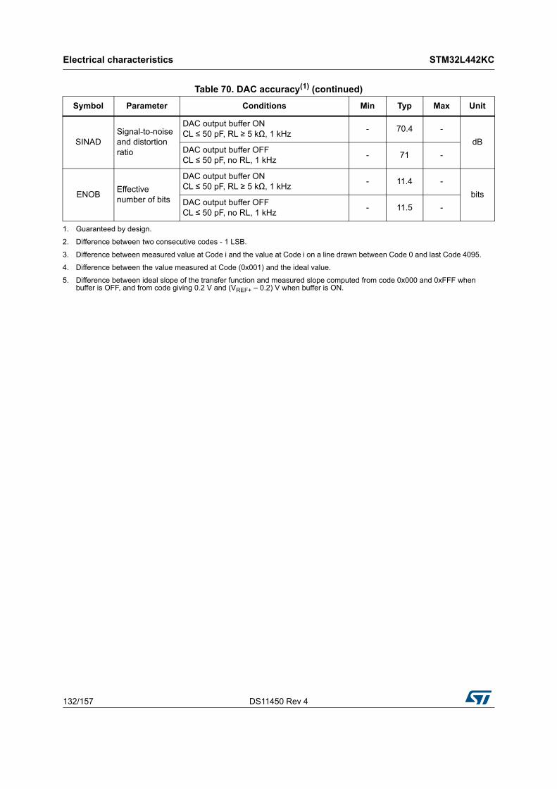
Electrical characteristics STM32L442KC
132/157 DS11450 Rev 4
SINADSignal-to-noise and distortion ratio
DAC output buffer ON CL ≤ 50 pF, RL ≥ 5 kΩ, 1 kHz
- 70.4 -
dBDAC output buffer OFF CL ≤ 50 pF, no RL, 1 kHz
- 71 -
ENOBEffective number of bits
DAC output buffer ON CL ≤ 50 pF, RL ≥ 5 kΩ, 1 kHz
- 11.4 -
bitsDAC output buffer OFF CL ≤ 50 pF, no RL, 1 kHz
- 11.5 -
1. Guaranteed by design.
2. Difference between two consecutive codes - 1 LSB.
3. Difference between measured value at Code i and the value at Code i on a line drawn between Code 0 and last Code 4095.
4. Difference between the value measured at Code (0x001) and the ideal value.
5. Difference between ideal slope of the transfer function and measured slope computed from code 0x000 and 0xFFF when buffer is OFF, and from code giving 0.2 V and (VREF+ – 0.2) V when buffer is ON.
Table 70. DAC accuracy(1) (continued)
Symbol Parameter Conditions Min Typ Max Unit
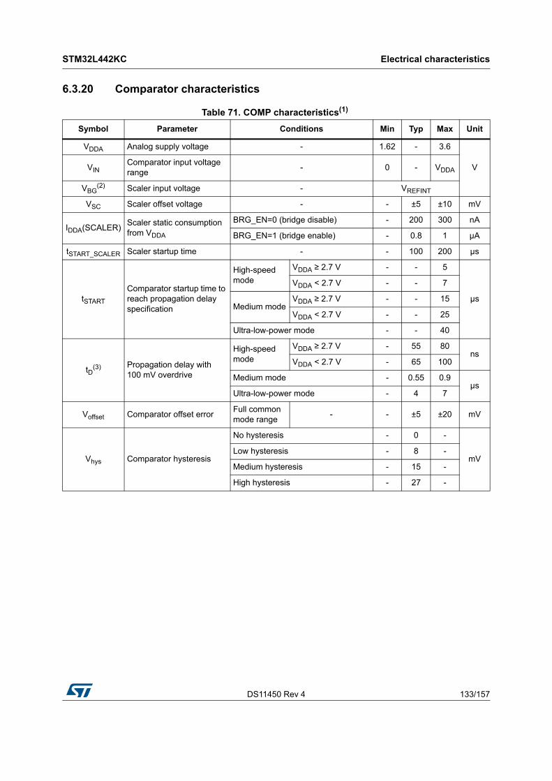
DS11450 Rev 4 133/157
STM32L442KC Electrical characteristics
149
6.3.20 Comparator characteristics
Table 71. COMP characteristics(1)
Symbol Parameter Conditions Min Typ Max Unit
VDDA Analog supply voltage - 1.62 - 3.6
VVINComparator input voltage range
- 0 - VDDA
VBG(2) Scaler input voltage - VREFINT
VSC Scaler offset voltage - - ±5 ±10 mV
IDDA(SCALER)Scaler static consumption from VDDA
BRG_EN=0 (bridge disable) - 200 300 nA
BRG_EN=1 (bridge enable) - 0.8 1 µA
tSTART_SCALER Scaler startup time - - 100 200 µs
tSTART
Comparator startup time to reach propagation delay specification
High-speed mode
VDDA ≥ 2.7 V - - 5
µs
VDDA < 2.7 V - - 7
Medium modeVDDA ≥ 2.7 V - - 15
VDDA < 2.7 V - - 25
Ultra-low-power mode - - 40
tD(3) Propagation delay with
100 mV overdrive
High-speed mode
VDDA ≥ 2.7 V - 55 80ns
VDDA < 2.7 V - 65 100
Medium mode - 0.55 0.9µs
Ultra-low-power mode - 4 7
Voffset Comparator offset errorFull common mode range
- - ±5 ±20 mV
Vhys Comparator hysteresis
No hysteresis - 0 -
mVLow hysteresis - 8 -
Medium hysteresis - 15 -
High hysteresis - 27 -
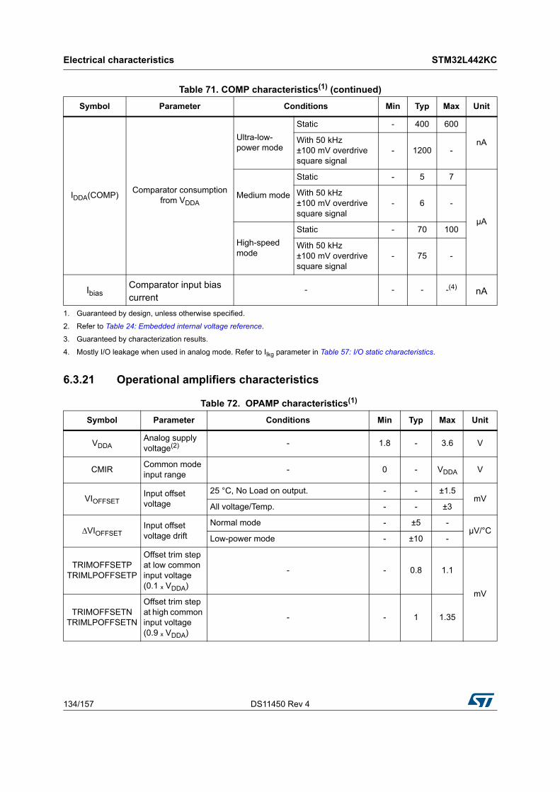
Electrical characteristics STM32L442KC
134/157 DS11450 Rev 4
6.3.21 Operational amplifiers characteristics
IDDA(COMP)Comparator consumption
from VDDA
Ultra-low-power mode
Static - 400 600
nAWith 50 kHz ±100 mV overdrive square signal
- 1200 -
Medium mode
Static - 5 7
µA
With 50 kHz ±100 mV overdrive square signal
- 6 -
High-speed mode
Static - 70 100
With 50 kHz ±100 mV overdrive square signal
- 75 -
IbiasComparator input bias current
- - - -(4) nA
1. Guaranteed by design, unless otherwise specified.
2. Refer to Table 24: Embedded internal voltage reference.
3. Guaranteed by characterization results.
4. Mostly I/O leakage when used in analog mode. Refer to Ilkg parameter in Table 57: I/O static characteristics.
Table 71. COMP characteristics(1) (continued)
Symbol Parameter Conditions Min Typ Max Unit
Table 72. OPAMP characteristics(1)
Symbol Parameter Conditions Min Typ Max Unit
VDDAAnalog supply voltage(2) - 1.8 - 3.6 V
CMIRCommon mode input range
- 0 - VDDA V
VIOFFSETInput offset voltage
25 °C, No Load on output. - - ±1.5mV
All voltage/Temp. - - ±3
∆VIOFFSETInput offset voltage drift
Normal mode - ±5 -μV/°C
Low-power mode - ±10 -
TRIMOFFSETPTRIMLPOFFSETP
Offset trim step at low common input voltage (0.1 ₓ VDDA)
- - 0.8 1.1
mV
TRIMOFFSETNTRIMLPOFFSETN
Offset trim step at high common input voltage (0.9 ₓ VDDA)
- - 1 1.35
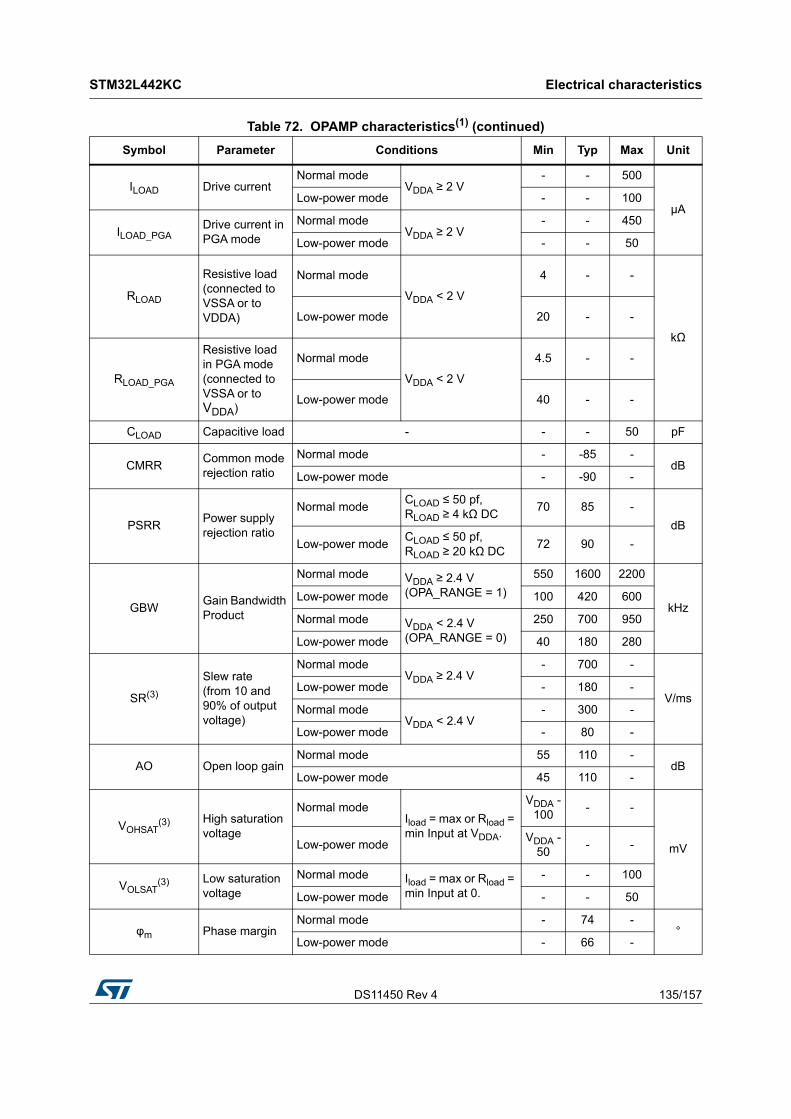
DS11450 Rev 4 135/157
STM32L442KC Electrical characteristics
149
ILOAD Drive currentNormal mode
VDDA ≥ 2 V- - 500
µALow-power mode - - 100
ILOAD_PGADrive current in PGA mode
Normal modeVDDA ≥ 2 V
- - 450
Low-power mode - - 50
RLOAD
Resistive load (connected to VSSA or to VDDA)
Normal mode
VDDA < 2 V
4 - -
kΩ
Low-power mode 20 - -
RLOAD_PGA
Resistive load in PGA mode (connected to VSSA or to VDDA)
Normal mode
VDDA < 2 V
4.5 - -
Low-power mode 40 - -
CLOAD Capacitive load - - - 50 pF
CMRRCommon mode rejection ratio
Normal mode - -85 -dB
Low-power mode - -90 -
PSRRPower supply rejection ratio
Normal modeCLOAD ≤ 50 pf, RLOAD ≥ 4 kΩ DC
70 85 -
dB
Low-power modeCLOAD ≤ 50 pf, RLOAD ≥ 20 kΩ DC
72 90 -
GBWGain Bandwidth Product
Normal mode VDDA ≥ 2.4 V (OPA_RANGE = 1)
550 1600 2200
kHzLow-power mode 100 420 600
Normal mode VDDA < 2.4 V (OPA_RANGE = 0)
250 700 950
Low-power mode 40 180 280
SR(3)
Slew rate (from 10 and 90% of output voltage)
Normal modeVDDA ≥ 2.4 V
- 700 -
V/msLow-power mode - 180 -
Normal modeVDDA < 2.4 V
- 300 -
Low-power mode - 80 -
AO Open loop gainNormal mode 55 110 -
dBLow-power mode 45 110 -
VOHSAT(3) High saturation
voltage
Normal modeIload = max or Rload = min Input at VDDA.
VDDA -100
- -
mVLow-power modeVDDA -
50- -
VOLSAT(3) Low saturation
voltage
Normal mode Iload = max or Rload = min Input at 0.
- - 100
Low-power mode - - 50
φm Phase marginNormal mode - 74 -
°Low-power mode - 66 -
Table 72. OPAMP characteristics(1) (continued)
Symbol Parameter Conditions Min Typ Max Unit
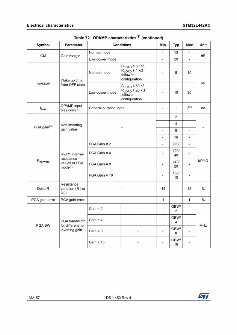
Electrical characteristics STM32L442KC
136/157 DS11450 Rev 4
GM Gain marginNormal mode - 13 -
dBLow-power mode - 20 -
tWAKEUPWake up time from OFF state.
Normal mode
CLOAD ≤ 50 pf, RLOAD ≥ 4 kΩ follower configuration
- 5 10
µs
Low-power mode
CLOAD ≤ 50 pf, RLOAD ≥ 20 kΩ follower configuration
- 10 30
IbiasOPAMP input bias current
General purpose input - - -(4) nA
PGA gain(3) Non inverting gain value
-
- 2 -
-- 4 -
- 8 -
- 16 -
Rnetwork
R2/R1 internal resistance values in PGA mode(5)
PGA Gain = 2 - 80/80 -
kΩ/kΩ
PGA Gain = 4 -120/40
-
PGA Gain = 8 -140/20
-
PGA Gain = 16 -150/10
-
Delta RResistance variation (R1 or R2)
- -15 - 15 %
PGA gain error PGA gain error - -1 - 1 %
PGA BWPGA bandwidth for different non inverting gain
Gain = 2 - -GBW/
2-
MHz
Gain = 4 - -GBW/
4-
Gain = 8 - -GBW/
8-
Gain = 16 - -GBW/
16-
Table 72. OPAMP characteristics(1) (continued)
Symbol Parameter Conditions Min Typ Max Unit
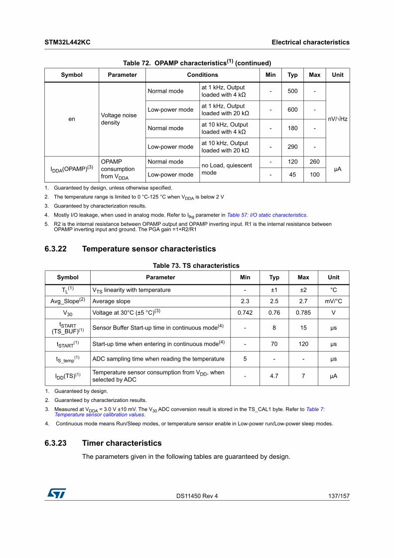
DS11450 Rev 4 137/157
STM32L442KC Electrical characteristics
149
6.3.22 Temperature sensor characteristics
6.3.23 Timer characteristics
The parameters given in the following tables are guaranteed by design.
enVoltage noise density
Normal modeat 1 kHz, Output loaded with 4 kΩ
- 500 -
nV/√Hz
Low-power modeat 1 kHz, Output loaded with 20 kΩ
- 600 -
Normal modeat 10 kHz, Output loaded with 4 kΩ
- 180 -
Low-power modeat 10 kHz, Output loaded with 20 kΩ
- 290 -
IDDA(OPAMP)(3)OPAMP consumption from VDDA
Normal modeno Load, quiescent mode
- 120 260µA
Low-power mode - 45 100
1. Guaranteed by design, unless otherwise specified.
2. The temperature range is limited to 0 °C-125 °C when VDDA is below 2 V
3. Guaranteed by characterization results.
4. Mostly I/O leakage, when used in analog mode. Refer to Ilkg parameter in Table 57: I/O static characteristics.
5. R2 is the internal resistance between OPAMP output and OPAMP inverting input. R1 is the internal resistance between OPAMP inverting input and ground. The PGA gain =1+R2/R1
Table 72. OPAMP characteristics(1) (continued)
Symbol Parameter Conditions Min Typ Max Unit
Table 73. TS characteristics
Symbol Parameter Min Typ Max Unit
TL(1) VTS linearity with temperature - ±1 ±2 °C
Avg_Slope(2) Average slope 2.3 2.5 2.7 mV/°C
V30 Voltage at 30°C (±5 °C)(3) 0.742 0.76 0.785 V
tSTART(TS_BUF)(1) Sensor Buffer Start-up time in continuous mode(4) - 8 15 µs
tSTART(1) Start-up time when entering in continuous mode(4) - 70 120 µs
tS_temp(1) ADC sampling time when reading the temperature 5 - - µs
IDD(TS)(1) Temperature sensor consumption from VDD, when selected by ADC
- 4.7 7 µA
1. Guaranteed by design.
2. Guaranteed by characterization results.
3. Measured at VDDA = 3.0 V ±10 mV. The V30 ADC conversion result is stored in the TS_CAL1 byte. Refer to Table 7: Temperature sensor calibration values.
4. Continuous mode means Run/Sleep modes, or temperature sensor enable in Low-power run/Low-power sleep modes.
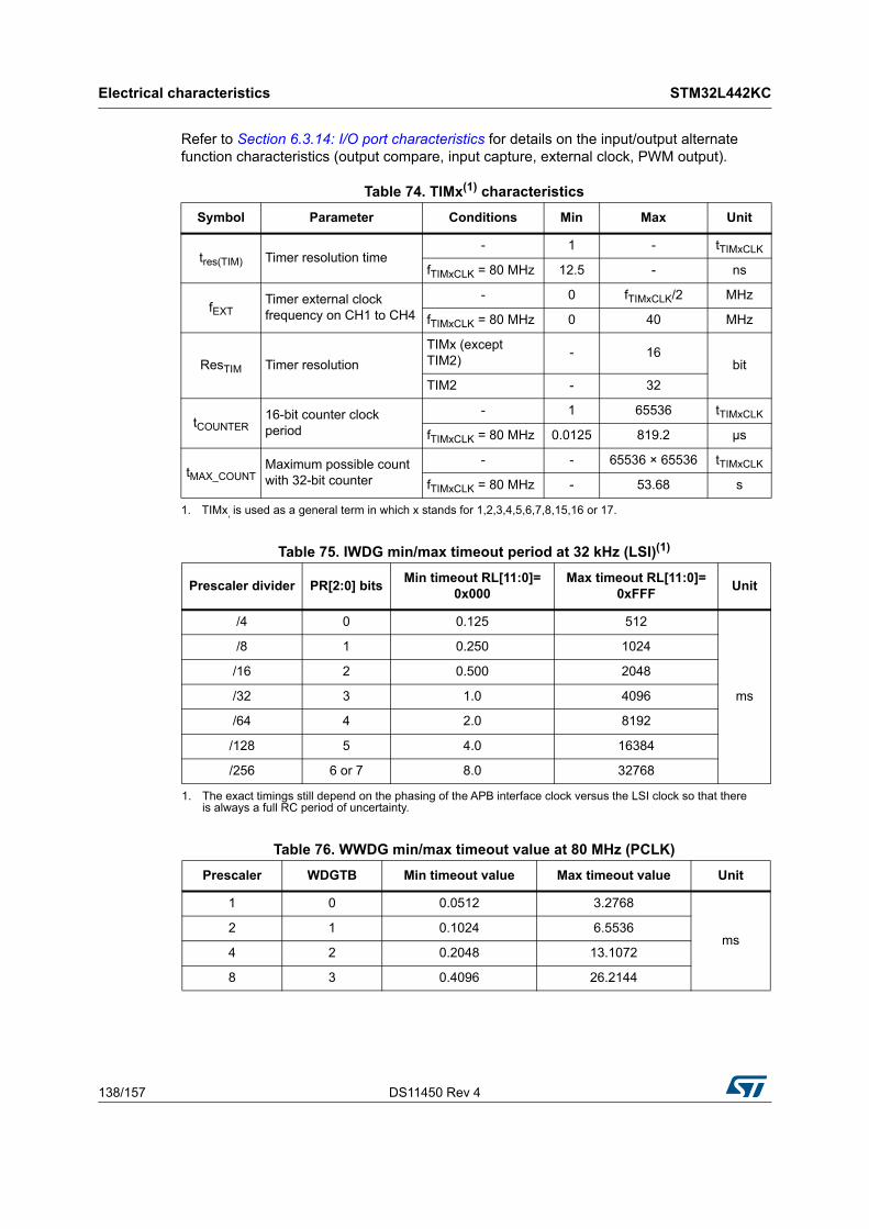
Electrical characteristics STM32L442KC
138/157 DS11450 Rev 4
Refer to Section 6.3.14: I/O port characteristics for details on the input/output alternate function characteristics (output compare, input capture, external clock, PWM output).
Table 74. TIMx(1) characteristics
1. TIMx, is used as a general term in which x stands for 1,2,3,4,5,6,7,8,15,16 or 17.
Symbol Parameter Conditions Min Max Unit
tres(TIM) Timer resolution time- 1 - tTIMxCLK
fTIMxCLK = 80 MHz 12.5 - ns
fEXTTimer external clock frequency on CH1 to CH4
- 0 fTIMxCLK/2 MHz
fTIMxCLK = 80 MHz 0 40 MHz
ResTIM Timer resolution
TIMx (except TIM2)
- 16bit
TIM2 - 32
tCOUNTER16-bit counter clock period
- 1 65536 tTIMxCLK
fTIMxCLK = 80 MHz 0.0125 819.2 µs
tMAX_COUNTMaximum possible count with 32-bit counter
- - 65536 × 65536 tTIMxCLK
fTIMxCLK = 80 MHz - 53.68 s
Table 75. IWDG min/max timeout period at 32 kHz (LSI)(1)
1. The exact timings still depend on the phasing of the APB interface clock versus the LSI clock so that there is always a full RC period of uncertainty.
Prescaler divider PR[2:0] bitsMin timeout RL[11:0]=
0x000Max timeout RL[11:0]=
0xFFFUnit
/4 0 0.125 512
ms
/8 1 0.250 1024
/16 2 0.500 2048
/32 3 1.0 4096
/64 4 2.0 8192
/128 5 4.0 16384
/256 6 or 7 8.0 32768
Table 76. WWDG min/max timeout value at 80 MHz (PCLK)
Prescaler WDGTB Min timeout value Max timeout value Unit
1 0 0.0512 3.2768
ms2 1 0.1024 6.5536
4 2 0.2048 13.1072
8 3 0.4096 26.2144
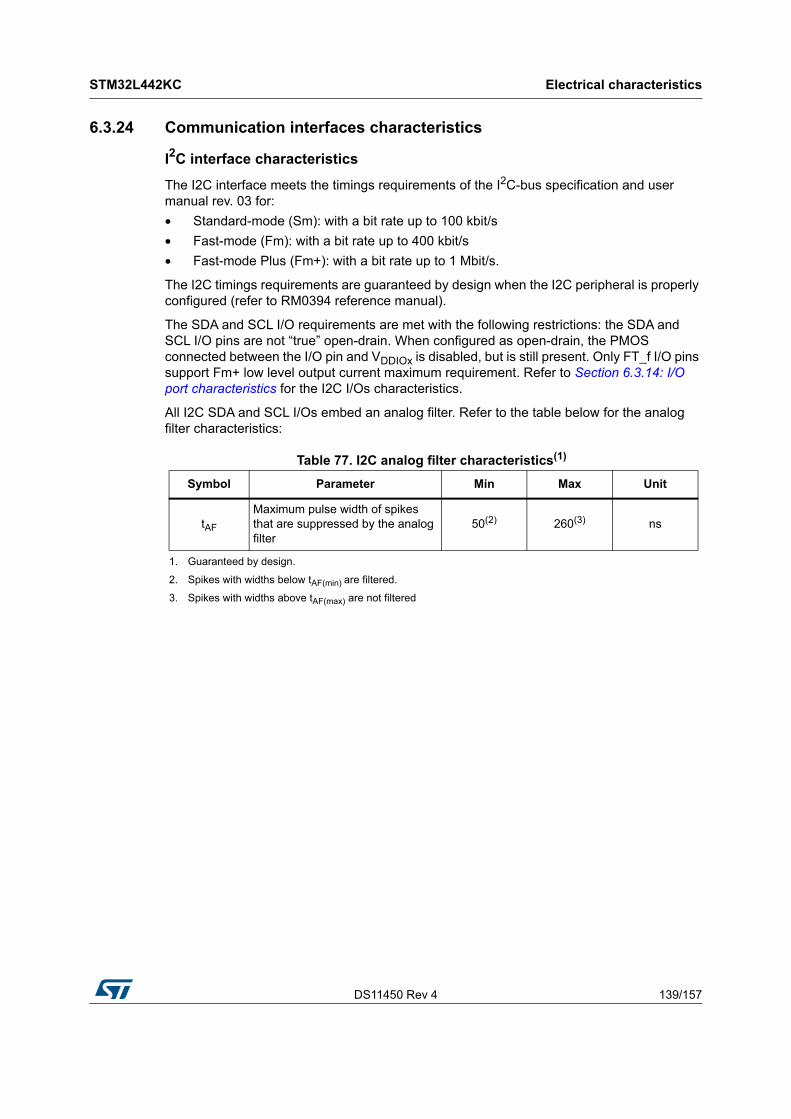
DS11450 Rev 4 139/157
STM32L442KC Electrical characteristics
149
6.3.24 Communication interfaces characteristics
I2C interface characteristics
The I2C interface meets the timings requirements of the I2C-bus specification and user manual rev. 03 for:
• Standard-mode (Sm): with a bit rate up to 100 kbit/s
• Fast-mode (Fm): with a bit rate up to 400 kbit/s
• Fast-mode Plus (Fm+): with a bit rate up to 1 Mbit/s.
The I2C timings requirements are guaranteed by design when the I2C peripheral is properly configured (refer to RM0394 reference manual).
The SDA and SCL I/O requirements are met with the following restrictions: the SDA and SCL I/O pins are not “true” open-drain. When configured as open-drain, the PMOS connected between the I/O pin and VDDIOx is disabled, but is still present. Only FT_f I/O pins support Fm+ low level output current maximum requirement. Refer to Section 6.3.14: I/O port characteristics for the I2C I/Os characteristics.
All I2C SDA and SCL I/Os embed an analog filter. Refer to the table below for the analog filter characteristics:
Table 77. I2C analog filter characteristics(1)
1. Guaranteed by design.
Symbol Parameter Min Max Unit
tAF
Maximum pulse width of spikes that are suppressed by the analog filter
50(2)
2. Spikes with widths below tAF(min) are filtered.
260(3)
3. Spikes with widths above tAF(max) are not filtered
ns
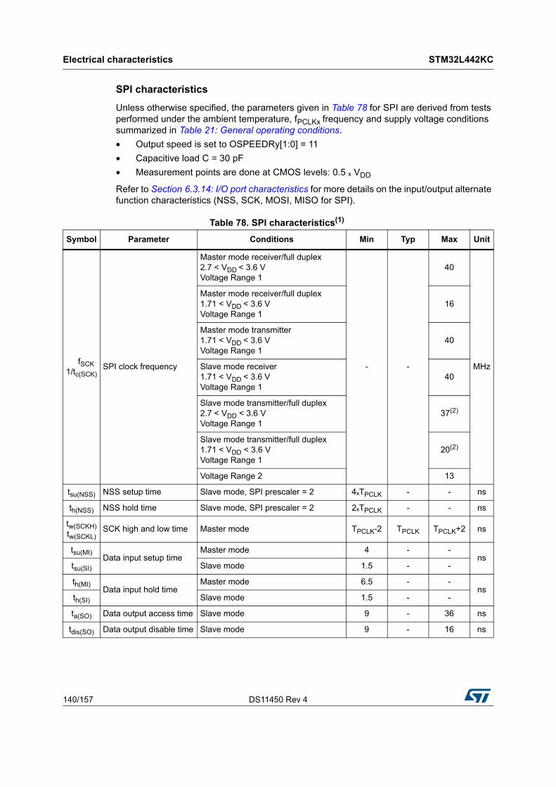
Electrical characteristics STM32L442KC
140/157 DS11450 Rev 4
SPI characteristics
Unless otherwise specified, the parameters given in Table 78 for SPI are derived from tests performed under the ambient temperature, fPCLKx frequency and supply voltage conditions summarized in Table 21: General operating conditions.
• Output speed is set to OSPEEDRy[1:0] = 11
• Capacitive load C = 30 pF
• Measurement points are done at CMOS levels: 0.5 ₓ VDD
Refer to Section 6.3.14: I/O port characteristics for more details on the input/output alternate function characteristics (NSS, SCK, MOSI, MISO for SPI).
Table 78. SPI characteristics(1)
Symbol Parameter Conditions Min Typ Max Unit
fSCK1/tc(SCK)
SPI clock frequency
Master mode receiver/full duplex 2.7 < VDD < 3.6 V Voltage Range 1
- -
40
MHz
Master mode receiver/full duplex 1.71 < VDD < 3.6 V Voltage Range 1
16
Master mode transmitter 1.71 < VDD < 3.6 V Voltage Range 1
40
Slave mode receiver 1.71 < VDD < 3.6 V Voltage Range 1
40
Slave mode transmitter/full duplex 2.7 < VDD < 3.6 V Voltage Range 1
37(2)
Slave mode transmitter/full duplex 1.71 < VDD < 3.6 V Voltage Range 1
20(2)
Voltage Range 2 13
tsu(NSS) NSS setup time Slave mode, SPI prescaler = 2 4ₓTPCLK - - ns
th(NSS) NSS hold time Slave mode, SPI prescaler = 2 2ₓTPCLK - - ns
tw(SCKH)tw(SCKL)
SCK high and low time Master mode TPCLK-2 TPCLK TPCLK+2 ns
tsu(MI)Data input setup time
Master mode 4 - -ns
tsu(SI) Slave mode 1.5 - -
th(MI)Data input hold time
Master mode 6.5 - -ns
th(SI) Slave mode 1.5 - -
ta(SO) Data output access time Slave mode 9 - 36 ns
tdis(SO) Data output disable time Slave mode 9 - 16 ns
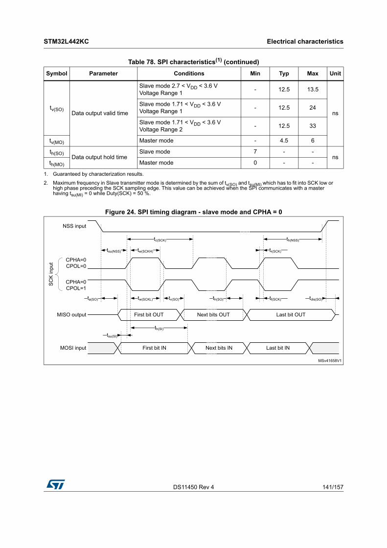
DS11450 Rev 4 141/157
STM32L442KC Electrical characteristics
149
Figure 24. SPI timing diagram - slave mode and CPHA = 0
tv(SO)Data output valid time
Slave mode 2.7 < VDD < 3.6 V Voltage Range 1
- 12.5 13.5
ns
Slave mode 1.71 < VDD < 3.6 V Voltage Range 1
- 12.5 24
Slave mode 1.71 < VDD < 3.6 V Voltage Range 2
- 12.5 33
tv(MO) Master mode - 4.5 6
th(SO)Data output hold time
Slave mode 7 - -ns
th(MO) Master mode 0 - -
1. Guaranteed by characterization results.
2. Maximum frequency in Slave transmitter mode is determined by the sum of tv(SO) and tsu(MI) which has to fit into SCK low or high phase preceding the SCK sampling edge. This value can be achieved when the SPI communicates with a master having tsu(MI) = 0 while Duty(SCK) = 50 %.
Table 78. SPI characteristics(1) (continued)
Symbol Parameter Conditions Min Typ Max Unit
MSv41658V1
NSS input
CPHA=0CPOL=0
SC
K in
put
CPHA=0CPOL=1
MISO output
MOSI input
tsu(SI)
th(SI)
tw(SCKL)
tw(SCKH)
tc(SCK)
tr(SCK)
th(NSS)
tdis(SO)
tsu(NSS)
ta(SO) tv(SO)
Next bits IN
Last bit OUT
First bit IN
First bit OUT Next bits OUT
th(SO) tf(SCK)
Last bit IN
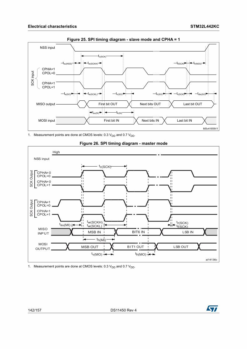
Electrical characteristics STM32L442KC
142/157 DS11450 Rev 4
Figure 25. SPI timing diagram - slave mode and CPHA = 1
1. Measurement points are done at CMOS levels: 0.3 VDD and 0.7 VDD.
Figure 26. SPI timing diagram - master mode
1. Measurement points are done at CMOS levels: 0.3 VDD and 0.7 VDD.
MSv41659V1
NSS input
CPHA=1CPOL=0
SC
K in
put
CPHA=1CPOL=1
MISO output
MOSI input
tsu(SI) th(SI)
tw(SCKL)
tw(SCKH)tsu(NSS)
tc(SCK)
ta(SO) tv(SO)
First bit OUT Next bits OUT
Next bits IN
Last bit OUT
th(SO) tr(SCK)
tf(SCK) th(NSS)
tdis(SO)
First bit IN Last bit IN
ai14136c
SCK
Out
put
CPHA=0
MOSIOUTPUT
MISOINPUT
CPHA=0
LSB OUT
LSB IN
CPOL=0
CPOL=1
BIT1 OUT
NSS input
tc(SCK)
tw(SCKH)tw(SCKL)
tr(SCK)tf(SCK)
th(MI)
High
SCK
Out
put
CPHA=1
CPHA=1
CPOL=0
CPOL=1
tsu(MI)
tv(MO) th(MO)
MSB IN BIT6 IN
MSB OUT
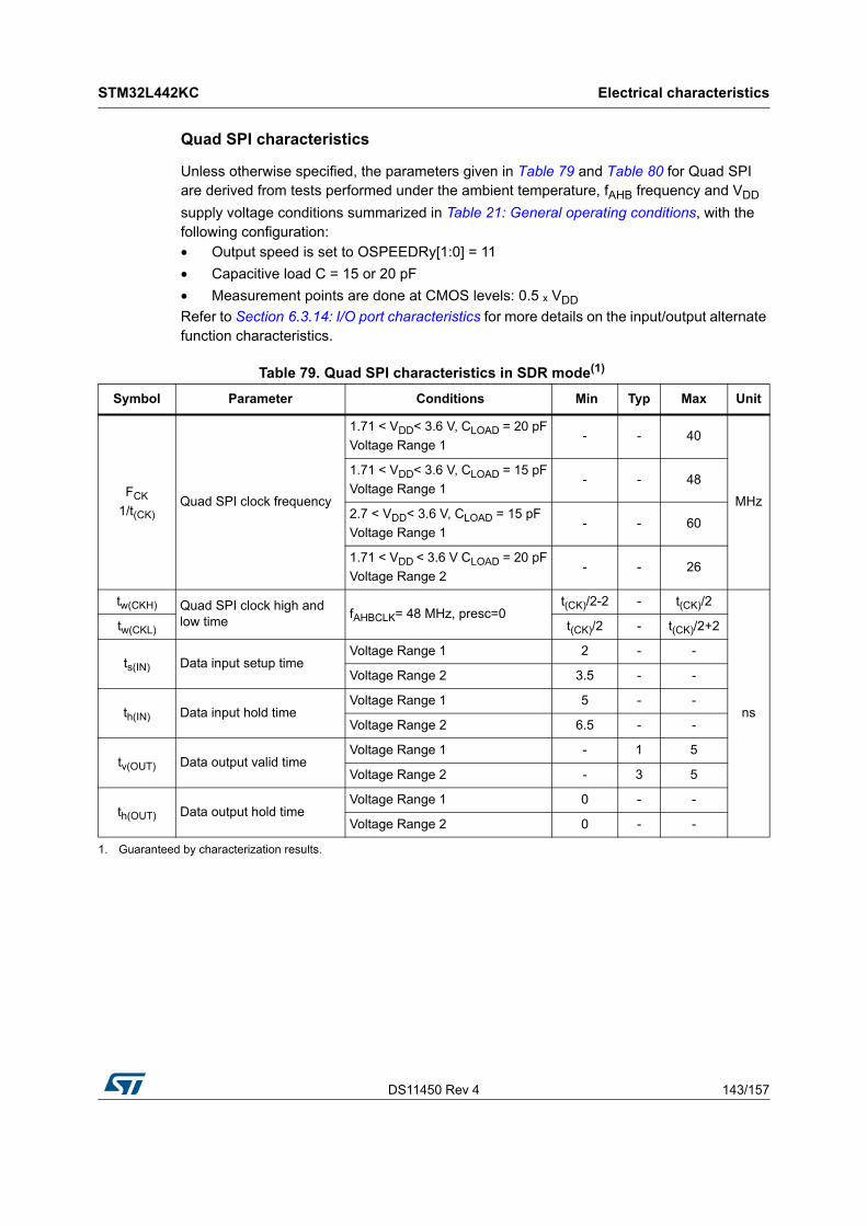
DS11450 Rev 4 143/157
STM32L442KC Electrical characteristics
149
Quad SPI characteristics
Unless otherwise specified, the parameters given in Table 79 and Table 80 for Quad SPI are derived from tests performed under the ambient temperature, fAHB frequency and VDD
supply voltage conditions summarized in Table 21: General operating conditions, with the following configuration:• Output speed is set to OSPEEDRy[1:0] = 11
• Capacitive load C = 15 or 20 pF
• Measurement points are done at CMOS levels: 0.5 ₓ VDD
Refer to Section 6.3.14: I/O port characteristics for more details on the input/output alternate function characteristics.
Table 79. Quad SPI characteristics in SDR mode(1)
Symbol Parameter Conditions Min Typ Max Unit
FCK
1/t(CK)Quad SPI clock frequency
1.71 < VDD< 3.6 V, CLOAD = 20 pF
Voltage Range 1 - - 40
MHz
1.71 < VDD< 3.6 V, CLOAD = 15 pF
Voltage Range 1- - 48
2.7 < VDD< 3.6 V, CLOAD = 15 pF
Voltage Range 1- - 60
1.71 < VDD < 3.6 V CLOAD = 20 pF
Voltage Range 2 - - 26
tw(CKH) Quad SPI clock high and low time
fAHBCLK= 48 MHz, presc=0 t(CK)/2-2 - t(CK)/2
ns
tw(CKL) t(CK)/2 - t(CK)/2+2
ts(IN) Data input setup timeVoltage Range 1 2 - -
Voltage Range 2 3.5 - -
th(IN) Data input hold timeVoltage Range 1 5 - -
Voltage Range 2 6.5 - -
tv(OUT) Data output valid timeVoltage Range 1 - 1 5
Voltage Range 2 - 3 5
th(OUT) Data output hold timeVoltage Range 1 0 - -
Voltage Range 2 0 - -
1. Guaranteed by characterization results.

Electrical characteristics STM32L442KC
144/157 DS11450 Rev 4
Table 80. QUADSPI characteristics in DDR mode(1)
Symbol Parameter Conditions Min Typ Max Unit
FCK
1/t(CK)
Quad SPI clock frequency
1.71 < VDD < 3.6 V, CLOAD = 20 pF
Voltage Range 1 - - 40
MHz
2 < VDD < 3.6 V, CLOAD = 20 pF
Voltage Range 1- - 48
1.71 < VDD < 3.6 V, CLOAD = 15 pF
Voltage Range 1- - 48
1.71 < VDD < 3.6 V CLOAD = 20 pF
Voltage Range 2- - 26
tw(CKH) Quad SPI clock high and low time
fAHBCLK = 48 MHz, presc=0 t(CK)/2-2 - t(CK)/2
ns
tw(CKL) t(CK)/2 - t(CK)/2+2
tsr(IN)Data input setup time on rising edge
Voltage Range 1 1- -
Voltage Range 2 3.5
tsf(IN)Data input setup time on falling edge
Voltage Range 1 1- -
Voltage Range 2 1.5
thr(IN)Data input hold time on rising edge
Voltage Range 1 6- -
Voltage Range 2 6.5
thf(IN)Data input hold time on falling edge
Voltage Range 1 5.5- -
Voltage Range 2 5.5
tvr(OUT)Data output valid time on rising edge
Voltage Range 1-
5 5.5
Voltage Range 2 9.5 14
tvf(OUT)Data output valid time on falling edge
Voltage Range 1-
5 8.5
Voltage Range 2 15 19
thr(OUT)Data output hold time on rising edge
Voltage Range 1 3.5 --
Voltage Range 2 8 -
thf(OUT)Data output hold time on falling edge
Voltage Range 1 3.5 --
Voltage Range 2 13 -
1. Guaranteed by characterization results.
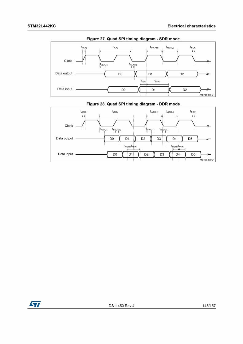
DS11450 Rev 4 145/157
STM32L442KC Electrical characteristics
149
Figure 27. Quad SPI timing diagram - SDR mode
Figure 28. Quad SPI timing diagram - DDR mode
MSv36878V1
Data output D0 D1 D2
Clock
Data input D0 D1 D2
t(CK) tw(CKH) tw(CKL)tr(CK) tf(CK)
ts(IN) th(IN)
tv(OUT) th(OUT)
MSv36879V1
Data output D0 D2 D4
Clock
Data input D0 D2 D4
t(CK) tw(CKH) tw(CKL)tr(CK) tf(CK)
tsf(IN) thf(IN)
tvf(OUT) thr(OUT)
D1 D3 D5
D1 D3 D5
tvr(OUT) thf(OUT)
tsr(IN) thr(IN)

Electrical characteristics STM32L442KC
146/157 DS11450 Rev 4
SAI characteristics
Unless otherwise specified, the parameters given in Table 81 for SAI are derived from tests performed under the ambient temperature, fPCLKx frequency and VDD
supply voltage conditions summarized inTable 21: General operating conditions, with the following configuration:• Output speed is set to OSPEEDRy[1:0] = 10
• Capacitive load C = 30 pF
• Measurement points are done at CMOS levels: 0.5 ₓ VDD
Refer to Section 6.3.14: I/O port characteristics for more details on the input/output alternate function characteristics (CK,SD,FS).
Table 81. SAI characteristics(1)
Symbol Parameter Conditions Min Max Unit
fMCLK SAI Main clock output - - 50 MHz
fCK SAI clock frequency(2)
Master transmitter 2.7 ≤ VDD ≤ 3.6 Voltage Range 1
- 18.5
MHz
Master transmitter 1.71 ≤ VDD ≤ 3.6 Voltage Range 1
- 12.5
Master receiver Voltage Range 1
- 25
Slave transmitter 2.7 ≤ VDD ≤ 3.6 Voltage Range 1
- 22.5
Slave transmitter 1.71 ≤ VDD ≤ 3.6 Voltage Range 1
- 14.5
Slave receiver Voltage Range 1
- 25
Voltage Range 2 - 12.5
tv(FS) FS valid time
Master mode 2.7 ≤ VDD ≤ 3.6
- 22
nsMaster mode 1.71 ≤ VDD ≤ 3.6
- 40
th(FS) FS hold time Master mode 10 - ns
tsu(FS) FS setup time Slave mode 1 - ns
th(FS) FS hold time Slave mode 2 - ns
tsu(SD_A_MR)Data input setup time
Master receiver 2 -ns
tsu(SD_B_SR) Slave receiver 1.5 -
th(SD_A_MR)Data input hold time
Master receiver 5 -ns
th(SD_B_SR) Slave receiver 2.5 -
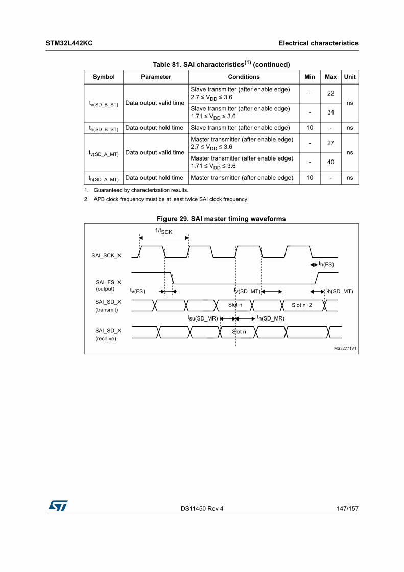
DS11450 Rev 4 147/157
STM32L442KC Electrical characteristics
149
Figure 29. SAI master timing waveforms
tv(SD_B_ST) Data output valid time
Slave transmitter (after enable edge) 2.7 ≤ VDD ≤ 3.6
- 22
nsSlave transmitter (after enable edge) 1.71 ≤ VDD ≤ 3.6
- 34
th(SD_B_ST) Data output hold time Slave transmitter (after enable edge) 10 - ns
tv(SD_A_MT) Data output valid time
Master transmitter (after enable edge) 2.7 ≤ VDD ≤ 3.6
- 27
nsMaster transmitter (after enable edge) 1.71 ≤ VDD ≤ 3.6
- 40
th(SD_A_MT) Data output hold time Master transmitter (after enable edge) 10 - ns
1. Guaranteed by characterization results.
2. APB clock frequency must be at least twice SAI clock frequency.
Table 81. SAI characteristics(1) (continued)
Symbol Parameter Conditions Min Max Unit
MS32771V1
SAI_SCK_X
SAI_FS_X(output)
1/fSCK
SAI_SD_X(transmit)
tv(FS)
Slot n
SAI_SD_X(receive)
th(FS)
Slot n+2
tv(SD_MT) th(SD_MT)
Slot n
tsu(SD_MR) th(SD_MR)
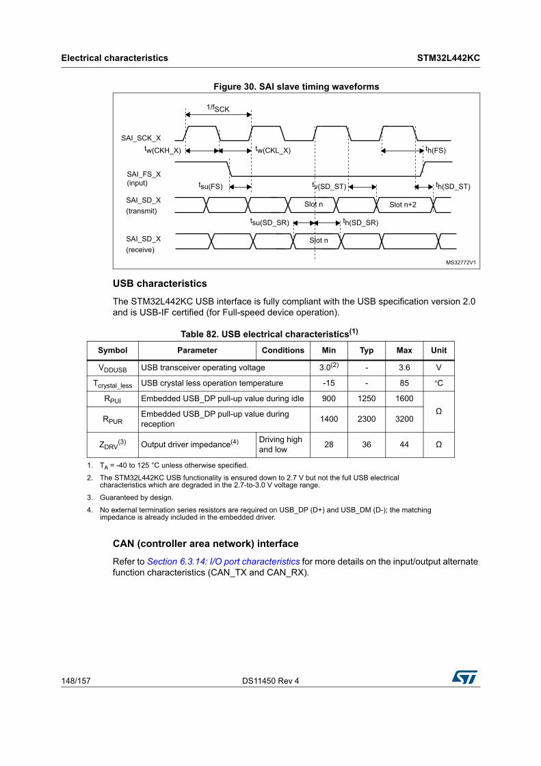
Electrical characteristics STM32L442KC
148/157 DS11450 Rev 4
Figure 30. SAI slave timing waveforms
USB characteristics
The STM32L442KC USB interface is fully compliant with the USB specification version 2.0 and is USB-IF certified (for Full-speed device operation).
CAN (controller area network) interface
Refer to Section 6.3.14: I/O port characteristics for more details on the input/output alternate function characteristics (CAN_TX and CAN_RX).
MS32772V1
SAI_SCK_X
SAI_FS_X(input)
SAI_SD_X(transmit)
tsu(FS)
Slot n
SAI_SD_X(receive)
tw(CKH_X) th(FS)
Slot n+2
tv(SD_ST) th(SD_ST)
Slot n
tsu(SD_SR)
tw(CKL_X)
th(SD_SR)
1/fSCK
Table 82. USB electrical characteristics(1)
Symbol Parameter Conditions Min Typ Max Unit
VDDUSB USB transceiver operating voltage 3.0(2) - 3.6 V
Tcrystal_less USB crystal less operation temperature -15 - 85 °C
RPUI Embedded USB_DP pull-up value during idle 900 1250 1600
ΩRPUR
Embedded USB_DP pull-up value during reception
1400 2300 3200
ZDRV(3) Output driver impedance(4) Driving high
and low28 36 44 Ω
1. TA = -40 to 125 °C unless otherwise specified.
2. The STM32L442KC USB functionality is ensured down to 2.7 V but not the full USB electrical characteristics which are degraded in the 2.7-to-3.0 V voltage range.
3. Guaranteed by design.
4. No external termination series resistors are required on USB_DP (D+) and USB_DM (D-); the matching impedance is already included in the embedded driver.
DS11450 Rev 4 149/157
STM32L442KC Electrical characteristics
149
SWPMI characteristics
The Single Wire Protocol Master Interface (SWPMI) and the associated SWPMI_IO transceiver are compliant with the ETSI TS 102 613 technical specification.
Table 83. SWPMI electrical characteristics
Symbol Parameter Conditions Min Typ Max Unit
tSWPSTART SWPMI regulator startup timeSWP Class B
2.7 V ≤ VDD ≤ 3,3V- - 300 μs
tSWPBIT SWP bit durationVCORE voltage range 1 500 - -
nsVCORE voltage range 2 620 - -
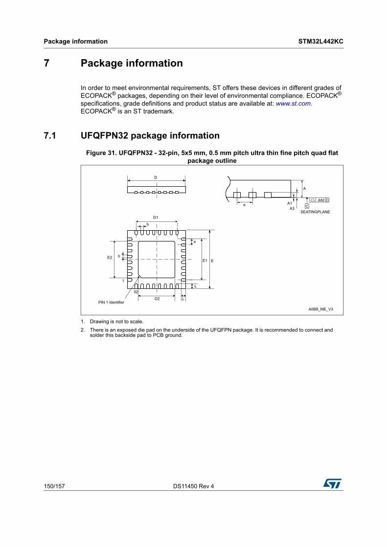
Package information STM32L442KC
150/157 DS11450 Rev 4
7 Package information
In order to meet environmental requirements, ST offers these devices in different grades of ECOPACK® packages, depending on their level of environmental compliance. ECOPACK® specifications, grade definitions and product status are available at: www.st.com. ECOPACK® is an ST trademark.
7.1 UFQFPN32 package information
Figure 31. UFQFPN32 - 32-pin, 5x5 mm, 0.5 mm pitch ultra thin fine pitch quad flat package outline
1. Drawing is not to scale.
2. There is an exposed die pad on the underside of the UFQFPN package. It is recommended to connect and solder this backside pad to PCB ground.
A0B8_ME_V3
1
32
PIN 1 Identifier
SEATINGPLANEC
Cddd
A
A1A3
e
b
D1
bE2
L
e
E1 E
D2 L
D
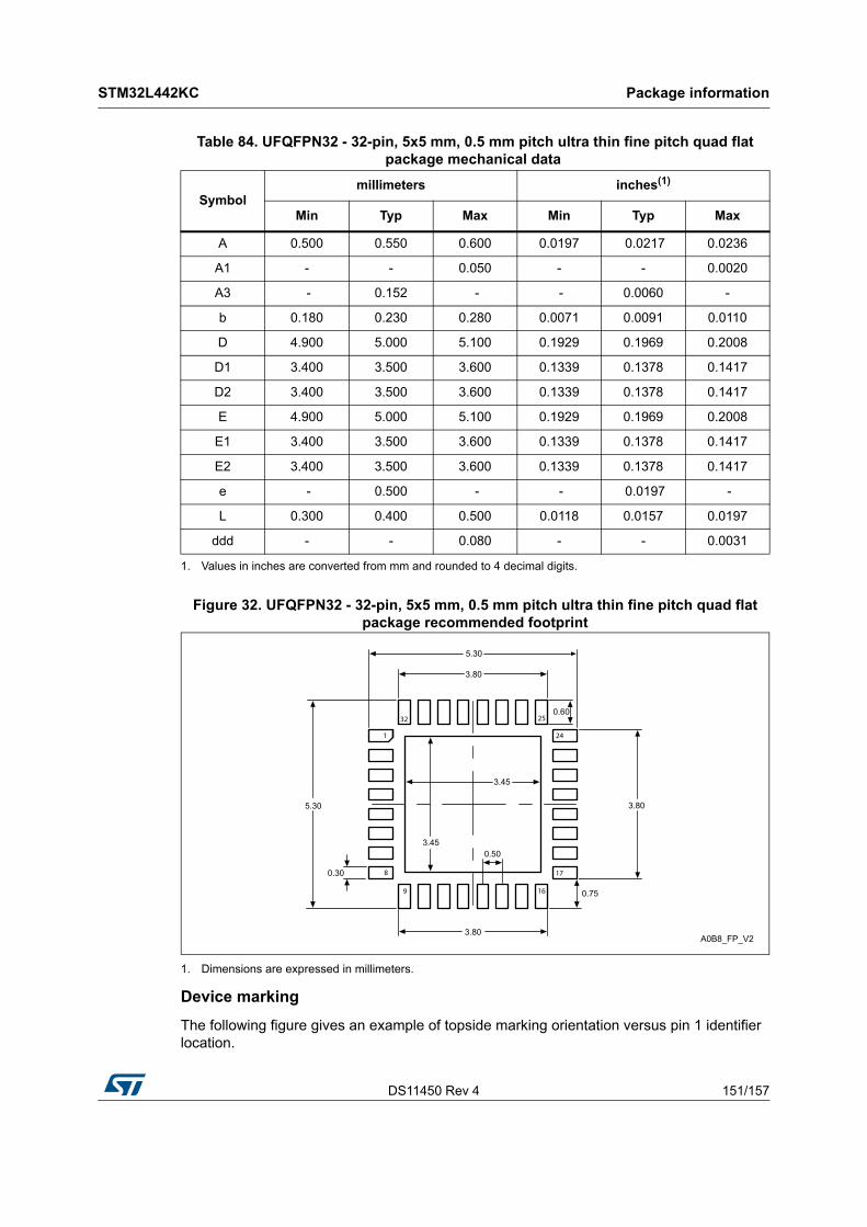
DS11450 Rev 4 151/157
STM32L442KC Package information
153
Figure 32. UFQFPN32 - 32-pin, 5x5 mm, 0.5 mm pitch ultra thin fine pitch quad flat package recommended footprint
1. Dimensions are expressed in millimeters.
Device marking
The following figure gives an example of topside marking orientation versus pin 1 identifier location.
Table 84. UFQFPN32 - 32-pin, 5x5 mm, 0.5 mm pitch ultra thin fine pitch quad flat package mechanical data
Symbolmillimeters inches(1)
1. Values in inches are converted from mm and rounded to 4 decimal digits.
Min Typ Max Min Typ Max
A 0.500 0.550 0.600 0.0197 0.0217 0.0236
A1 - - 0.050 - - 0.0020
A3 - 0.152 - - 0.0060 -
b 0.180 0.230 0.280 0.0071 0.0091 0.0110
D 4.900 5.000 5.100 0.1929 0.1969 0.2008
D1 3.400 3.500 3.600 0.1339 0.1378 0.1417
D2 3.400 3.500 3.600 0.1339 0.1378 0.1417
E 4.900 5.000 5.100 0.1929 0.1969 0.2008
E1 3.400 3.500 3.600 0.1339 0.1378 0.1417
E2 3.400 3.500 3.600 0.1339 0.1378 0.1417
e - 0.500 - - 0.0197 -
L 0.300 0.400 0.500 0.0118 0.0157 0.0197
ddd - - 0.080 - - 0.0031
A0B8_FP_V2
5.30
3.80
0.60
3.45
0.503.45
3.80
0.75
3.80
0.30
5.30
16
17
9
8
1
2532
24
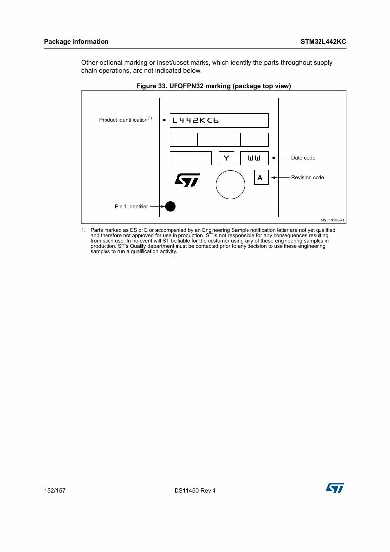
Package information STM32L442KC
152/157 DS11450 Rev 4
Other optional marking or inset/upset marks, which identify the parts throughout supply chain operations, are not indicated below.
Figure 33. UFQFPN32 marking (package top view)
1. Parts marked as ES or E or accompanied by an Engineering Sample notification letter are not yet qualified and therefore not approved for use in production. ST is not responsible for any consequences resulting from such use. In no event will ST be liable for the customer using any of these engineering samples in production. ST’s Quality department must be contacted prior to any decision to use these engineering samples to run a qualification activity.
MSv40150V1
Date code
Pin 1 identifier
Product identification(1)
Revision codeA
WWY
L442KC6

DS11450 Rev 4 153/157
STM32L442KC Package information
153
7.2 Thermal characteristics
The maximum chip junction temperature (TJmax) must never exceed the values given in Table 21: General operating conditions.
The maximum chip-junction temperature, TJ max, in degrees Celsius, may be calculated using the following equation:
TJ max = TA max + (PD max x ΘJA)
Where:
• TA max is the maximum ambient temperature in °C,
• ΘJA is the package junction-to-ambient thermal resistance, in °C/W,
• PD max is the sum of PINT max and PI/O max (PD max = PINT max + PI/Omax),
• PINT max is the product of all IDDXXX and VDDXXX, expressed in Watts. This is the maximum chip internal power.
PI/O max represents the maximum power dissipation on output pins where:
PI/O max = Σ (VOL × IOL) + Σ ((VDDIOx – VOH) × IOH),
taking into account the actual VOL / IOL and VOH / IOH of the I/Os at low and high level in the application.
7.2.1 Reference document
JESD51-2 Integrated Circuits Thermal Test Method Environment Conditions - Natural Convection (Still Air). Available from www.jedec.org
Table 85. Package thermal characteristics
Symbol Parameter Value Unit
ΘJAThermal resistance junction-ambient UFQFPN32 - 5 × 5 mm / 0.5 mm pitch
39 °C/W
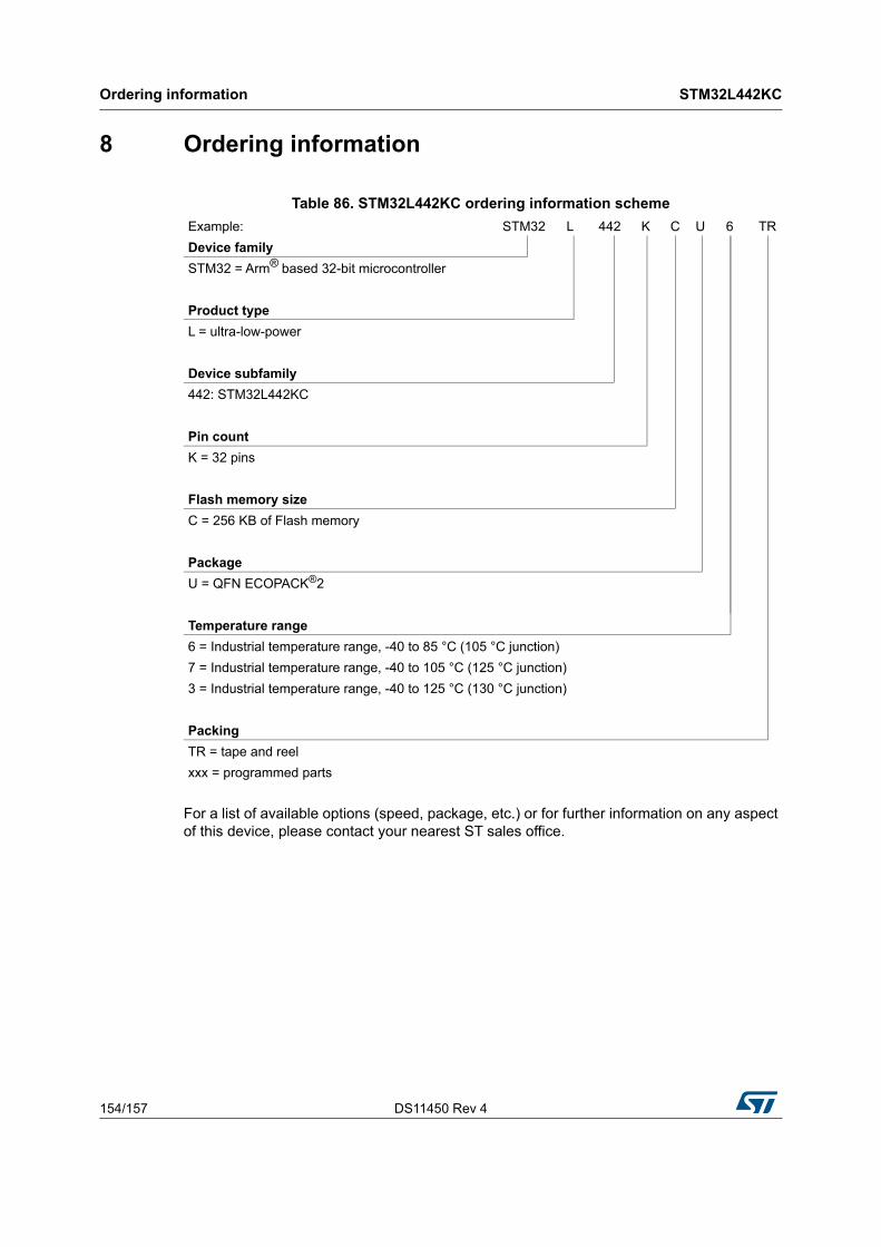
Ordering information STM32L442KC
154/157 DS11450 Rev 4
8 Ordering information
For a list of available options (speed, package, etc.) or for further information on any aspect of this device, please contact your nearest ST sales office.
Table 86. STM32L442KC ordering information scheme
Example: STM32 L 442 K C U 6 TR
Device family
STM32 = Arm® based 32-bit microcontroller
Product type
L = ultra-low-power
Device subfamily
442: STM32L442KC
Pin count
K = 32 pins
Flash memory size
C = 256 KB of Flash memory
Package
U = QFN ECOPACK®2
Temperature range
6 = Industrial temperature range, -40 to 85 °C (105 °C junction)
7 = Industrial temperature range, -40 to 105 °C (125 °C junction)
3 = Industrial temperature range, -40 to 125 °C (130 °C junction)
Packing
TR = tape and reel
xxx = programmed parts
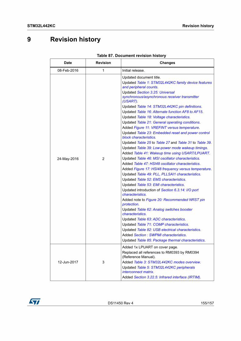
DS11450 Rev 4 155/157
STM32L442KC Revision history
156
9 Revision history
Table 87. Document revision history
Date Revision Changes
08-Feb-2016 1 Initial release.
24-May-2016 2
Updated document title.
Updated Table 1: STM32L442KC family device features and peripheral counts.
Updated Section 3.25: Universal synchronous/asynchronous receiver transmitter (USART).
Updated Table 14: STM32L442KC pin definitions.
Updated Table 16: Alternate function AF8 to AF15.
Updated Table 18: Voltage characteristics.
Updated Table 21: General operating conditions.
Added Figure 11: VREFINT versus temperature.
Updated Table 23: Embedded reset and power control block characteristics.
Updated Table 25 to Table 27 and Table 31 to Table 39.
Updated Table 39: Low-power mode wakeup timings.
Added Table 41: Wakeup time using USART/LPUART.
Updated Table 46: MSI oscillator characteristics.
Added Table 47: HSI48 oscillator characteristics.
Added Figure 17: HSI48 frequency versus temperature.
Updated Table 49: PLL, PLLSAI1 characteristics.
Updated Table 52: EMS characteristics.
Updated Table 53: EMI characteristics.
Updated introduction of Section 6.3.14: I/O port characteristics.
Added note to Figure 20: Recommended NRST pin protection.
Updated Table 62: Analog switches booster characteristics.
Updated Table 63: ADC characteristics.
Updated Table 71: COMP characteristics.
Updated Table 82: USB electrical characteristics.
Added Section : SWPMI characteristics.
Updated Table 85: Package thermal characteristics.
12-Jun-2017 3
Added 1x LPUART on cover page.
Replaced all references to RM0393 by RM0394 (Reference Manual).
Added Table 3: STM32L442KC modes overview.
Updated Table 5: STM32L442KC peripherals interconnect matrix.
Added Section 3.22.5: Infrared interface (IRTIM).
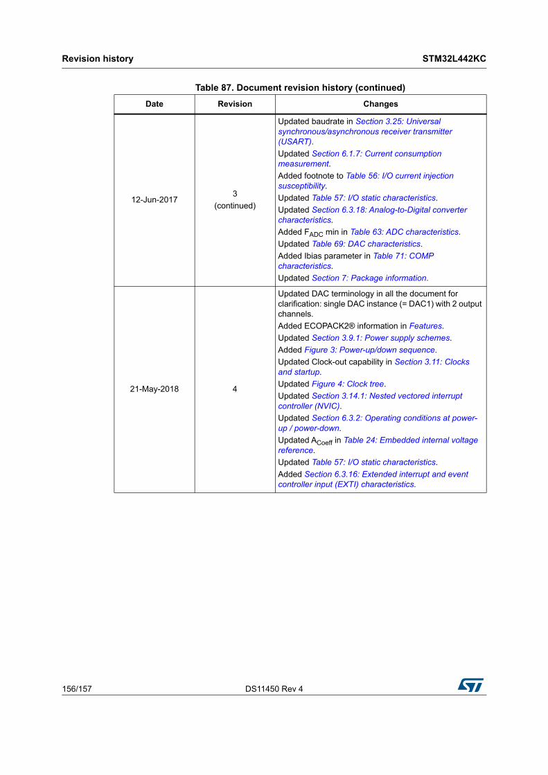
Revision history STM32L442KC
156/157 DS11450 Rev 4
12-Jun-20173
(continued)
Updated baudrate in Section 3.25: Universal synchronous/asynchronous receiver transmitter (USART).
Updated Section 6.1.7: Current consumption measurement.
Added footnote to Table 56: I/O current injection susceptibility.
Updated Table 57: I/O static characteristics.
Updated Section 6.3.18: Analog-to-Digital converter characteristics.
Added FADC min in Table 63: ADC characteristics.
Updated Table 69: DAC characteristics.
Added Ibias parameter in Table 71: COMP characteristics.
Updated Section 7: Package information.
21-May-2018 4
Updated DAC terminology in all the document for clarification: single DAC instance (= DAC1) with 2 output channels.
Added ECOPACK2® information in Features.
Updated Section 3.9.1: Power supply schemes.
Added Figure 3: Power-up/down sequence.
Updated Clock-out capability in Section 3.11: Clocks and startup.
Updated Figure 4: Clock tree.
Updated Section 3.14.1: Nested vectored interrupt controller (NVIC).
Updated Section 6.3.2: Operating conditions at power-up / power-down.
Updated ACoeff in Table 24: Embedded internal voltage reference.
Updated Table 57: I/O static characteristics.
Added Section 6.3.16: Extended interrupt and event controller input (EXTI) characteristics.
Table 87. Document revision history (continued)
Date Revision Changes
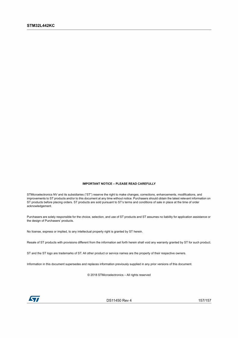
DS11450 Rev 4 157/157
STM32L442KC
157
IMPORTANT NOTICE – PLEASE READ CAREFULLY
STMicroelectronics NV and its subsidiaries (“ST”) reserve the right to make changes, corrections, enhancements, modifications, and improvements to ST products and/or to this document at any time without notice. Purchasers should obtain the latest relevant information on ST products before placing orders. ST products are sold pursuant to ST’s terms and conditions of sale in place at the time of order acknowledgement.
Purchasers are solely responsible for the choice, selection, and use of ST products and ST assumes no liability for application assistance or the design of Purchasers’ products.
No license, express or implied, to any intellectual property right is granted by ST herein.
Resale of ST products with provisions different from the information set forth herein shall void any warranty granted by ST for such product.
ST and the ST logo are trademarks of ST. All other product or service names are the property of their respective owners.
Information in this document supersedes and replaces information previously supplied in any prior versions of this document.
© 2018 STMicroelectronics – All rights reserved