Embed Size (px)
Citation preview
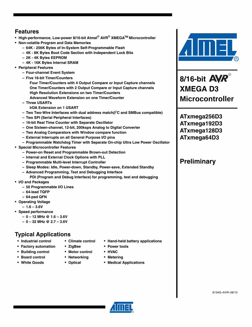
8/16-bitXMEGA D3Microcontroller
ATxmega256D3ATxmega192D3ATxmega128D3ATxmega64D3
Preliminary
8134G–AVR–08/10
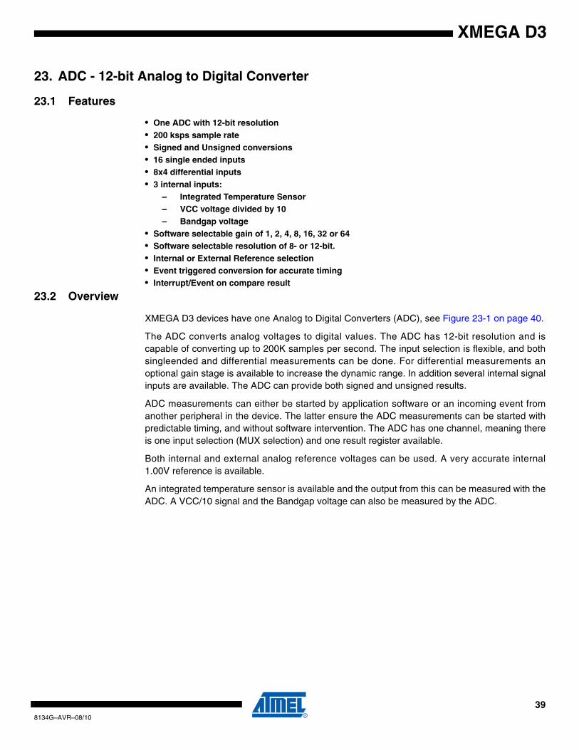
Features• High-performance, Low-power 8/16-bit Atmel® AVR® XMEGATM Microcontroller• Non-volatile Program and Data Memories
– 64K - 256K Bytes of In-System Self-Programmable Flash– 4K - 8K Bytes Boot Code Section with Independent Lock Bits– 2K - 4K Bytes EEPROM– 4K - 16K Bytes Internal SRAM
• Peripheral Features– Four-channel Event System– Five 16-bit Timer/Counters
Four Timer/Counters with 4 Output Compare or Input Capture channelsOne Timer/Counters with 2 Output Compare or Input Capture channelsHigh Resolution Extensions on two Timer/CountersAdvanced Waveform Extension on one Timer/Counter
– Three USARTsIrDA Extension on 1 USART
– Two Two-Wire Interfaces with dual address match(I2C and SMBus compatible)– Two SPI (Serial Peripheral Interfaces)– 16-bit Real Time Counter with Separate Oscillator– One Sixteen-channel, 12-bit, 200ksps Analog to Digital Converter– Two Analog Comparators with Window compare function– External Interrupts on all General Purpose I/O pins– Programmable Watchdog Timer with Separate On-chip Ultra Low Power Oscillator
• Special Microcontroller Features– Power-on Reset and Programmable Brown-out Detection– Internal and External Clock Options with PLL– Programmable Multi-level Interrupt Controller – Sleep Modes: Idle, Power-down, Standby, Power-save, Extended Standby– Advanced Programming, Test and Debugging Interface
PDI (Program and Debug Interface) for programming, test and debugging• I/O and Packages
– 50 Programmable I/O Lines– 64-lead TQFP– 64-pad QFN
• Operating Voltage– 1.6 – 3.6V
• Speed performance– 0 – 12 MHz @ 1.6 – 3.6V– 0 – 32 MHz @ 2.7 – 3.6V
Typical Applications • Industrial control • Climate control • Hand-held battery applications• Factory automation • ZigBee • Power tools• Building control • Motor control • HVAC• Board control • Networking • Metering• White Goods • Optical • Medical Applications
XMEGA D3
1. Ordering Information
Notes: 1. This device can also be supplied in wafer form. Please contact your local Atmel sales office for detailed ordering information.2. Pb-free packaging, complies to the European Directive for Restriction of Hazardous Substances (RoHS directive). Also Halide free and fully Green.3. For packaging information, see ”Packaging information” on page 86.
Ordering Code Flash (B) E2 (B) SRAM (B) Speed (MHz) Power Supply Package(1)(2)(3) Temp
ATxmega256D3-AU 256K + 8K 4K 16K 32 1.6 - 3.6V
64A
-40° - 85°C
ATxmega192D3-AU 192K + 8K 2K 16K 32 1.6 - 3.6V
ATxmega128D3-AU 128K + 8K 2K 8K 32 1.6 - 3.6V
ATxmega64D3-AU 64K + 4K 2K 4K 32 1.6 - 3.6V
ATxmega256D3-MH 256K + 8K 4K 16K 32 1.6 - 3.6V
64M2ATxmega192D3-MH 192K + 8K 2K 16K 32 1.6 - 3.6V
ATxmega128D3-MH 128K + 8K 2K 8K 32 1.6 - 3.6V
ATxmega64D3-MH 64K + 4K 2K 4K 32 1.6 - 3.6V
Package Type
64A 64-lead, 14 x 14 mm Body Size, 1.0 mm Body Thickness, 0.8 mm Lead Pitch, Thin Profile Plastic Quad Flat Package (TQFP)
64M2 64-pad, 9 x 9 x 1.0 mm Body, Lead Pitch 0.50 mm, 7.65 mm Exposed Pad, Quad Flat No-Lead Package (QFN)
28134G–AVR–08/10
XMEGA D3
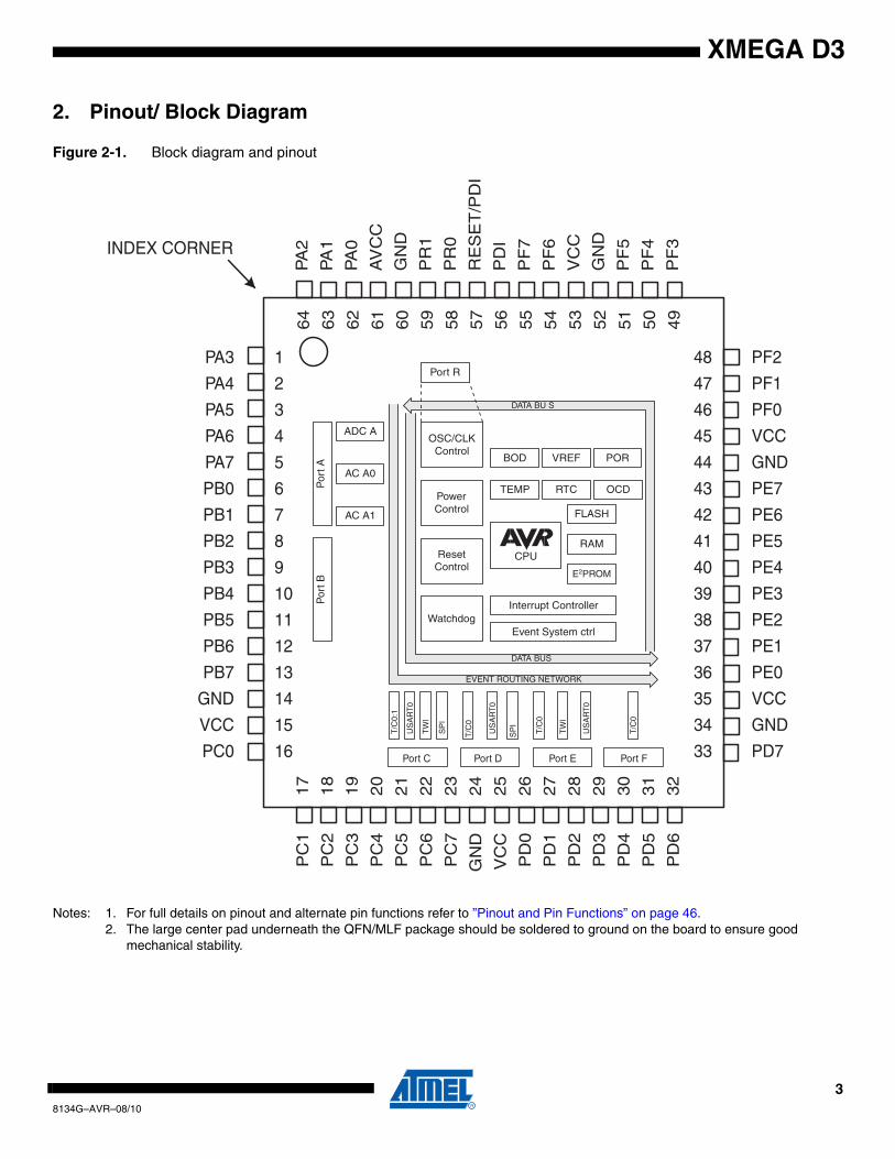
2. Pinout/ Block Diagram
Figure 2-1. Block diagram and pinout
Notes: 1. For full details on pinout and alternate pin functions refer to ”Pinout and Pin Functions” on page 46.2. The large center pad underneath the QFN/MLF package should be soldered to ground on the board to ensure good
mechanical stability.
INDEX CORNER
17
18
19
20
21
22
23
24
25
26
27
28
29
30
31
32
64
63
62
61
60
59
58
57
56
55
54
53
52
51
50
49
48
47
46
45
44
43
42
41
40
39
38
37
36
35
34
33
1
2
3
4
5
6
7
8
9
10
11
12
13
14
15
16
PF2
PF1
PF0
VCC
GND
PE7
PE6
PE5
PE4
PE3
PE2
PE1
PE0
VCC
GND
PD7
PA3
PA4
PA5
PA6
PA7
PB0
PB1
PB2
PB3
PB4
PB5
PB6
PB7
GND
VCC
PC0
PC
1
PC
2
PC
3
PC
4
PC
5
PC
6
PC
7
GN
D
VC
C
PD
0
PD
1
PD
2
PD
3
PD
4
PD
5
PD
6
PA
2
PA
1
PA
0
AV
CC
GN
D
PR
1
PR
0
RE
SE
T/P
DI
PD
I
PF
7
PF
6
VC
C
GN
D
PF
5
PF
4
PF
3
FLASH
RAM
E2PROM
Interrupt Controller
OCD
ADC A
AC A0
AC A1
Por
t AP
ort B
Event System ctrl
Port R
PowerControl
ResetControl
Watchdog
OSC/CLKControl
BOD POR
RTC
EVENT ROUTING NETWORK
DATA BUS
DATA BU S
VREF
TEMP
Port C Port D Port E Port F
CPU
T/C
0:1
US
AR
T0
SP
I
TW
I
T/C
0
US
AR
T0
SP
I
T/C
0
US
AR
T0
T/C
0
TW
I
38134G–AVR–08/10
XMEGA D3
3. Overview
The Atmel® AVR® XMEGA D3 is a family of low power, high performance and peripheral richCMOS 8/16-bit microcontrollers based on the AVR® enhanced RISC architecture. By execugpowerful instructions in a single clock cycle, the XMEGA D3 achieves throughputs approaching1 Million Instructions Per Second (MIPS) per MHz allowing the system designer to optimizepower consumption versus processing speed.
The AVR CPU combines a rich instruction set with 32 general purpose working registers. All the32 registers are directly connected to the Arithmetic Logic Unit (ALU), allowing two independentregisters to be accessed in one single instruction, executed in one clock cycle. The resultingarchitecture is more code efficient while achieving throughputs many times faster than conven-tional single-accumulator or CISC based microcontrollers.
The XMEGA D3 devices provide the following features: In-System Programmable Flash withRead-While-Write capabilities, Internal EEPROM and SRAM, four-channel Event System, Pro-grammable Multi-level Interrupt Controller, 50 general purpose I/O lines, 16-bit Real TimeCounter (RTC), five flexible 16-bit Timer/Counters with compare modes and PWM, threeUSARTs, two Two-Wire Interface (TWIs), two Serial Peripheral Interfaces (SPIs), one 16-chan-nel 12-bit ADC with optional differential input with programmable gain, two analog comparatorswith window mode, programmable Watchdog Timer with separate Internal Oscillator, accurateinternal oscillators with PLL and prescaler and programmable Brown-Out Detection.
The Program and Debug Interface (PDI), a fast 2-pin interface for programming and debugging,is available.
The XMEGA D3 devices have five software selectable power saving modes. The Idle modestops the CPU while allowing the SRAM, Event System, Interrupt Controller and all peripheralsto continue functioning. The Power-down mode saves the SRAM and register contents but stopsthe oscillators, disabling all other functions until the next TWI or pin-change interrupt, or Reset.In Power-save mode, the asynchronous Real Time Counter continues to run, allowing the appli-cation to maintain a timer base while the rest of the device is sleeping. In Standby mode, theCrystal/Resonator Oscillator is kept running while the rest of the device is sleeping. This allowsvery fast start-up from external crystal combined with low power consumption. In ExtendedStandby mode, both the main Oscillator and the Asynchronous Timer continue to run. To furtherreduce power consumption, the peripheral clock for each individual peripheral can optionally bestopped in Active mode and Idle sleep mode.
The device is manufactured using Atmel's high-density nonvolatile memory technology. The pro-gram Flash memory can be reprogrammed in-system through the PDI. A Bootloader running inthe device can use any interface to download the application program to the Flash memory. TheBootloader software in the Boot Flash section will continue to run while the Application Flashsection is updated, providing true Read-While-Write operation. By combining an 8/16-bit RISCCPU with In-System Self-Programmable Flash, the Atmel XMEGA D3 is a powerful microcon-troller family that provides a highly flexible and cost effective solution for many embeddedapplications.
The XMEGA D3 devices are supported with a full suite of program and system developmenttools including: C compilers, macro assemblers, program debugger/simulators, programmers,and evaluation kits.
48134G–AVR–08/10
XMEGA D3
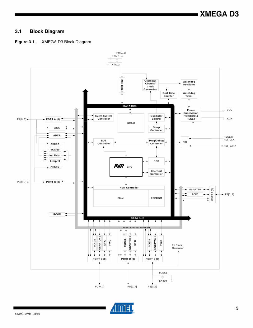
3.1 Block Diagram
Figure 3-1. XMEGA D3 Block Diagram
Power SupervisionPOR/BOD &
RESETPORT A (8)
PORT B (8)
BUS Controller
SRAM
ADCA
ACA
OCD
PDI
CPU
PA[0..7]
PB[0..7]
Watchdog Timer
WatchdogOscillator
Interrupt Controller
DATA BUS
Prog/DebugController
VCC
GNDPO
RT
R (2
)
XTAL1
XTAL2
PR[0..1]
Oscillator Circuits/
Clock Generation
Oscillator Control
Real TimeCounter
Event System Controller
PDI_DATA
RESET/PDI_CLK
Sleep Controller
Flash EEPROM
NVM Controller
IRCOM
PORT C (8)
PC[0..7]
TCC
0:1
USA
RTC
0:1
TWIC
SPIC
PD[0..7] PE[0..7]
PORT D (8)
TCD
0:1
USA
RTD
0:1
SPID
TCE0
:1
USA
RTE
0:1
Int. Refs.
AREFA
AREFB
Tempref
VCC/10
TOSC1
TOSC2
To Clock Generator
TCF0
USARTF0
POR
T F
(8)
PF[0..7]
EVENT ROUTING NETWORK
DATA BUS
PORT E (8)
TWIE
58134G–AVR–08/10
XMEGA D3
4. Resources
A comprehensive set of development tools, application notes and datasheets are available fordownload on http://www.atmel.com/avr.
4.1 Recommended reading
• Atmel® AVR® XMEGATM D Manual
• XMEGA Application Notes
This device data sheet only contains part specific information and a short description of eachperipheral and module. The XMEGA D Manual describes the modules and peripherals in depth.The XMEGA application notes contain example code and show applied use of the modules andperipherals.
The XMEGA Manual and Application Notes are available from http://www.atmel.com/avr.
5. Disclaimer
For devices that are not available yet, typical values contained in this datasheet are based onsimulations and characterization of other AVR XMEGA microcontrollers manufactured on thesame process technology. Min. and Max values will be available after the device ischaracterized.
68134G–AVR–08/10
XMEGA D3
6. AVR CPU
6.1 Features• 8/16-bit high performance AVR RISC Architecture
– 138 instructions– Hardware multiplier
• 32x8-bit registers directly connected to the ALU• Stack in RAM• Stack Pointer accessible in I/O memory space• Direct addressing of up to 16M bytes of program and data memory• True 16/24-bit access to 16/24-bit I/O registers• Support for 8-, 16- and 32-bit Arithmetic• Configuration Change Protection of system critical features
6.2 Overview
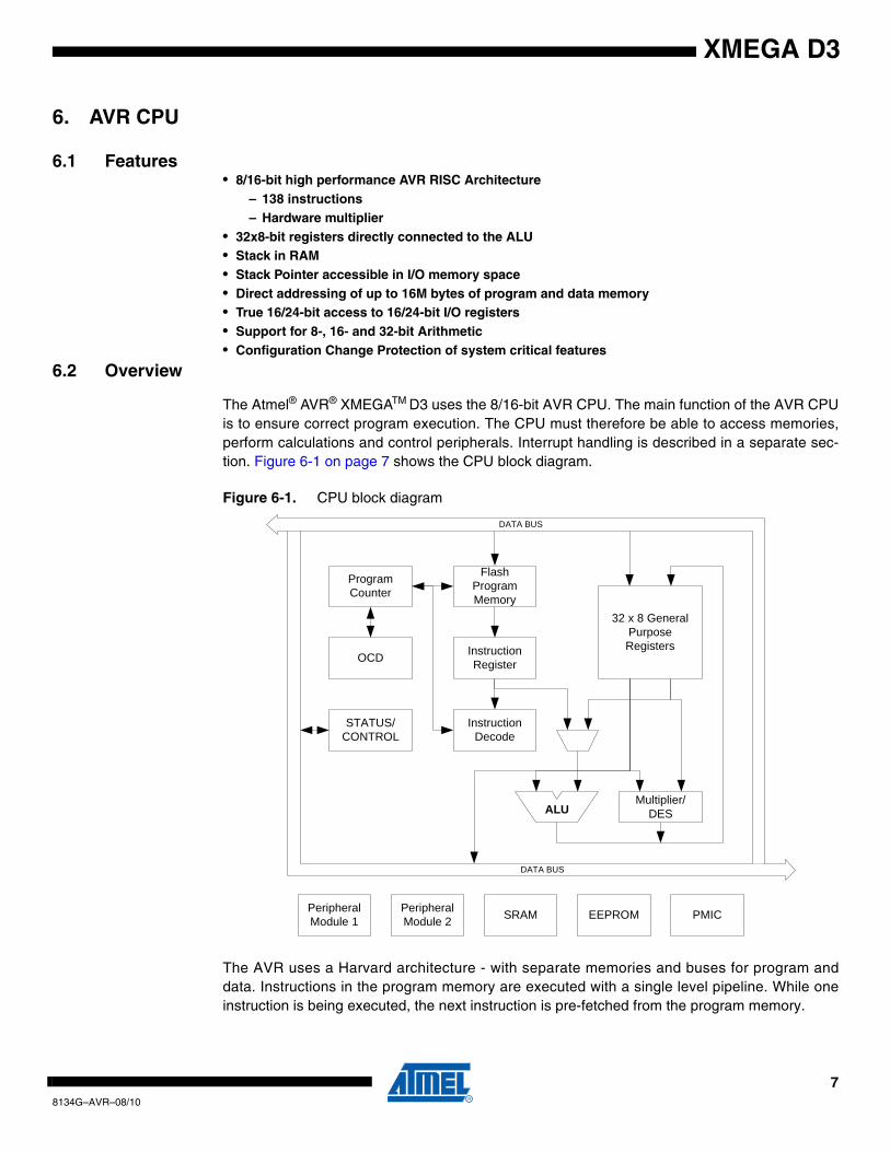
The Atmel® AVR® XMEGATM D3 uses the 8/16-bit AVR CPU. The main function of the AVR CPUis to ensure correct program execution. The CPU must therefore be able to access memories,perform calculations and control peripherals. Interrupt handling is described in a separate sec-tion. Figure 6-1 on page 7 shows the CPU block diagram.
Figure 6-1. CPU block diagram
The AVR uses a Harvard architecture - with separate memories and buses for program anddata. Instructions in the program memory are executed with a single level pipeline. While oneinstruction is being executed, the next instruction is pre-fetched from the program memory.
Flash Program Memory
InstructionDecode
Program Counter
OCD
32 x 8 General Purpose Registers
ALUMultiplier/
DES
InstructionRegister
STATUS/CONTROL
Peripheral Module 1
Peripheral Module 2 EEPROM PMICSRAM
DATA BUS
DATA BUS
78134G–AVR–08/10
XMEGA D3
This concept enables instructions to be executed in every clock cycle. The program memory isIn-System Re-programmable Flash memory.
6.3 Register File
The fast-access Register File contains 32 x 8-bit general purpose working registers with a singleclock cycle access time. This allows single-cycle Arithmetic Logic Unit (ALU) operation. In a typ-ical ALU operation, two operands are output from the Register File, the operation is executed,and the result is stored back in the Register File - in one clock cycle.
Six of the 32 registers can be used as three 16-bit indirect address register pointers for DataSpace addressing - enabling efficient address calculations. One of these address pointers canalso be used as an address pointer for look up tables in Flash program memory.
6.4 ALU - Arithmetic Logic Unit
The high performance Arithmetic Logic Unit (ALU) supports arithmetic and logic operationsbetween registers or between a constant and a register. Single register operations can also beexecuted. Within a single clock cycle, arithmetic operations between general purpose registersor between a register and an immediate are executed. After an arithmetic or logic operation, theStatus Register is updated to reflect information about the result of the operation.
The ALU operations are divided into three main categories – arithmetic, logical, and bit-func-tions. Both 8- and 16-bit arithmetic is supported, and the instruction set allows for easyimplementation of 32-bit arithmetic. The ALU also provides a powerful multiplier supporting bothsigned and unsigned multiplication and fractional format.
6.5 Program Flow
When the device is powered on, the CPU starts to execute instructions from the lowest addressin the Flash Program Memory ‘0’. The Program Counter (PC) addresses the next instruction tobe fetched. After a reset, the PC is set to location ‘0’.
Program flow is provided by conditional and unconditional jump and call instructions, capable ofaddressing the whole address space directly. Most AVR instructions use a 16-bit word format,while a limited number uses a 32-bit format.
During interrupts and subroutine calls, the return address PC is stored on the Stack. The Stackis effectively allocated in the general data SRAM, and consequently the Stack size is only limitedby the total SRAM size and the usage of the SRAM. After reset the Stack Pointer (SP) points tothe highest address in the internal SRAM. The SP is read/write accessible in the I/O memoryspace, enabling easy implementation of multiple stacks or stack areas. The data SRAM caneasily be accessed through the five different addressing modes supported in the AVR CPU.
88134G–AVR–08/10
XMEGA D3
7. Memories
7.1 Features• Flash Program Memory
– One linear address space– In-System Programmable– Self-Programming and Bootloader support– Application Section for application code– Application Table Section for application code or data storage– Boot Section for application code or bootloader code– Separate lock bits and protection for all sections
• Data Memory– One linear address space– Single cycle access from CPU– SRAM– EEPROM
Byte and page accessibleOptional memory mapping for direct load and store
– I/O MemoryConfiguration and Status registers for all peripherals and modules16 bit-accessible General Purpose Register for global variables or flags
• Production Signature Row Memory for factory programmed dataDevice ID for each microcontroller device typeSerial number for each deviceOscillator calibration bytesADC and temperature sensor calibration data
• User Signature RowOne flash page in sizeCan be read and written from softwareContent is kept after chip erase
7.2 Overview
The AVR architecture has two main memory spaces, the Program Memory and the Data Mem-ory. In addition, the XMEGA D3 features an EEPROM Memory for non-volatile data storage. Allthree memory spaces are linear and require no paging. The available memory size configura-tions are shown in ”Ordering Information” on page 2. In addition each device has a Flashmemory signature row for calibration data, device identification, serial number etc.
Non-volatile memory spaces can be locked for further write or read/write operations. This pre-vents unrestricted access to the application software.
7.3 In-System Programmable Flash Program Memory
The XMEGA D3 devices contains On-chip In-System Programmable Flash memory for programstorage, see Figure 7-1 on page 10. Since all AVR instructions are 16- or 32-bits wide, eachFlash address location is 16 bits.
The Program Flash memory space is divided into Application and Boot sections. Both sectionshave dedicated Lock Bits for setting restrictions on write or read/write operations. The Store Pro-
98134G–AVR–08/10
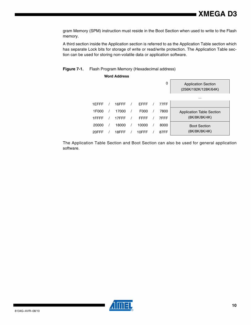
XMEGA D3
gram Memory (SPM) instruction must reside in the Boot Section when used to write to the Flashmemory.
A third section inside the Application section is referred to as the Application Table section whichhas separate Lock bits for storage of write or read/write protection. The Application Table sec-tion can be used for storing non-volatile data or application software.
The Application Table Section and Boot Section can also be used for general applicationsoftware.
Figure 7-1. Flash Program Memory (Hexadecimal address)
Word Address
0 Application Section(256K/192K/128K/64K)
...
1EFFF / 16FFF / EFFF / 77FF
1F000 / 17000 / F000 / 7800 Application Table Section
(8K/8K/8K/4K)1FFFF / 17FFF / FFFF / 7FFF
20000 / 18000 / 10000 / 8000 Boot Section(8K/8K/8K/4K)20FFF / 18FFF / 10FFF / 87FF
108134G–AVR–08/10
XMEGA D3
7.4 Data Memory
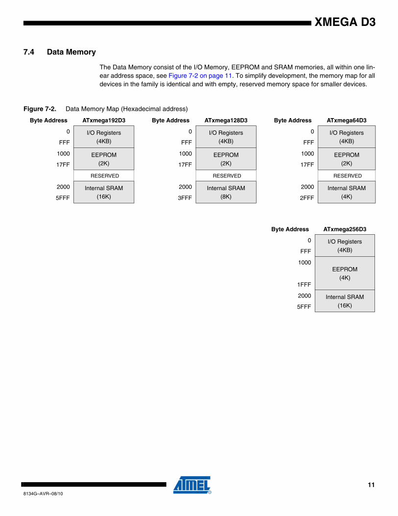
The Data Memory consist of the I/O Memory, EEPROM and SRAM memories, all within one lin-ear address space, see Figure 7-2 on page 11. To simplify development, the memory map for alldevices in the family is identical and with empty, reserved memory space for smaller devices.
Figure 7-2. Data Memory Map (Hexadecimal address)
Byte Address ATxmega192D3 Byte Address ATxmega128D3 Byte Address ATxmega64D3
0 I/O Registers
(4KB)
0 I/O Registers
(4KB)
0 I/O Registers
(4KB)FFF FFF FFF
1000 EEPROM(2K)
1000 EEPROM(2K)
1000 EEPROM(2K)17FF 17FF 17FF
RESERVED RESERVED RESERVED
2000 Internal SRAM(16K)
2000 Internal SRAM(8K)
2000 Internal SRAM(4K)5FFF 3FFF 2FFF
Byte Address ATxmega256D3
0 I/O Registers
(4KB)FFF
1000EEPROM
(4K)1FFF
2000 Internal SRAM
(16K)5FFF
118134G–AVR–08/10
XMEGA D3
7.4.1 I/O Memory
All peripherals and modules are addressable through I/O memory locations in the data memoryspace. All I/O memory locations can be accessed by the Load (LD/LDS/LDD) and Store(ST/STS/STD) instructions, transferring data between the 32 general purpose registers in theCPU and the I/O Memory.
The IN and OUT instructions can address I/O memory locations in the range 0x00 - 0x3Fdirectly.
I/O registers within the address range 0x00 - 0x1F are directly bit-accessible using the SBI andCBI instructions. The value of single bits can be checked by using the SBIS and SBIC instruc-tions on these registers.
The I/O memory address for all peripherals and modules in XMEGA D3 is shown in the ”Periph-eral Module Address Map” on page 51.
7.4.2 SRAM Data Memory
The XMEGA D3 devices have internal SRAM memory for data storage.
7.4.3 EEPROM Data Memory
The XMEGA D3 devices have internal EEPROM memory for non-volatile data storage. It isaddressable either in a separate data space or it can be memory mapped into the normal datamemory space. The EEPROM memory supports both byte and page access.
128134G–AVR–08/10
XMEGA D3
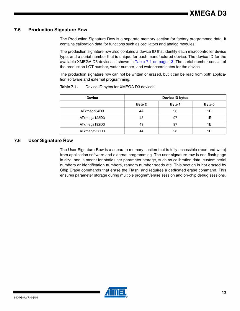
7.5 Production Signature Row
The Production Signature Row is a separate memory section for factory programmed data. Itcontains calibration data for functions such as oscillators and analog modules.
The production signature row also contains a device ID that identify each microcontroller devicetype, and a serial number that is unique for each manufactured device. The device ID for theavailable XMEGA D3 devices is shown in Table 7-1 on page 13. The serial number consist ofthe production LOT number, wafer number, and wafer coordinates for the device.
The production signature row can not be written or erased, but it can be read from both applica-tion software and external programming.
Table 7-1. Device ID bytes for XMEGA D3 devices.
7.6 User Signature Row
The User Signature Row is a separate memory section that is fully accessible (read and write)from application software and external programming. The user signature row is one flash pagein size, and is meant for static user parameter storage, such as calibration data, custom serialnumbers or identification numbers, random number seeds etc. This section is not erased byChip Erase commands that erase the Flash, and requires a dedicated erase command. Thisensures parameter storage during multiple program/erase session and on-chip debug sessions.
Device Device ID bytes
Byte 2 Byte 1 Byte 0
ATxmega64D3 4A 96 1E
ATxmega128D3 48 97 1E
ATxmega192D3 49 97 1E
ATxmega256D3 44 98 1E
138134G–AVR–08/10
XMEGA D3
7.7 Flash and EEPROM Page Size
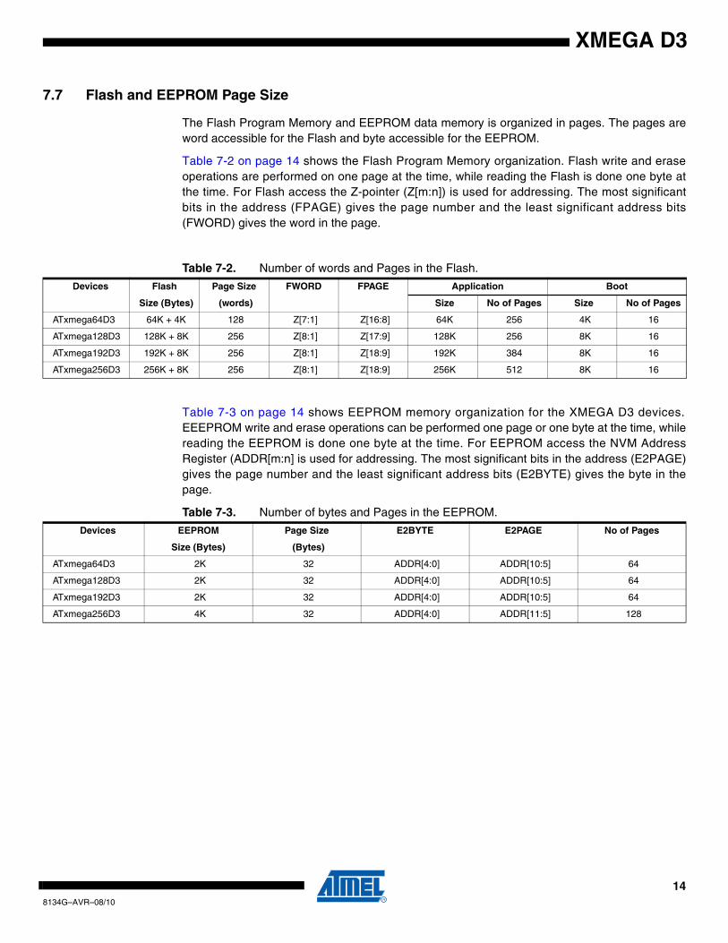
The Flash Program Memory and EEPROM data memory is organized in pages. The pages areword accessible for the Flash and byte accessible for the EEPROM.
Table 7-2 on page 14 shows the Flash Program Memory organization. Flash write and eraseoperations are performed on one page at the time, while reading the Flash is done one byte atthe time. For Flash access the Z-pointer (Z[m:n]) is used for addressing. The most significantbits in the address (FPAGE) gives the page number and the least significant address bits(FWORD) gives the word in the page.
Table 7-2. Number of words and Pages in the Flash.
Table 7-3 on page 14 shows EEPROM memory organization for the XMEGA D3 devices.EEEPROM write and erase operations can be performed one page or one byte at the time, whilereading the EEPROM is done one byte at the time. For EEPROM access the NVM AddressRegister (ADDR[m:n] is used for addressing. The most significant bits in the address (E2PAGE)gives the page number and the least significant address bits (E2BYTE) gives the byte in thepage.
Table 7-3. Number of bytes and Pages in the EEPROM.
Devices Flash Page Size FWORD FPAGE Application Boot
Size (Bytes) (words) Size No of Pages Size No of Pages
ATxmega64D3 64K + 4K 128 Z[7:1] Z[16:8] 64K 256 4K 16
ATxmega128D3 128K + 8K 256 Z[8:1] Z[17:9] 128K 256 8K 16
ATxmega192D3 192K + 8K 256 Z[8:1] Z[18:9] 192K 384 8K 16
ATxmega256D3 256K + 8K 256 Z[8:1] Z[18:9] 256K 512 8K 16
Devices EEPROM Page Size E2BYTE E2PAGE No of Pages
Size (Bytes) (Bytes)
ATxmega64D3 2K 32 ADDR[4:0] ADDR[10:5] 64
ATxmega128D3 2K 32 ADDR[4:0] ADDR[10:5] 64
ATxmega192D3 2K 32 ADDR[4:0] ADDR[10:5] 64
ATxmega256D3 4K 32 ADDR[4:0] ADDR[11:5] 128
148134G–AVR–08/10
XMEGA D3
8. Event System8.1 Features
• Inter-peripheral communication and signalling with minimum latency• CPU independent operation• 4 Event Channels allows for up to 4 signals to be routed at the same time• Events can be generated by
– Timer/Counters (TCxn)– Real Time Counter (RTC)– Analog to Digital Converters (ADC)– Analog Comparators (AC)– Ports (PORTx)– System Clock (ClkSYS)– Software (CPU)
• Events can be used by– Timer/Counters (TCxn)– Analog to Digital Converters (ADC)– Ports (PORTx)– IR Communication Module (IRCOM)
• The same event can be used by multiple peripherals for synchronized timing• Advanced Features
– Manual Event Generation from software (CPU)– Quadrature Decoding– Digital Filtering
• Functions in Active and Idle mode
8.2 Overview
The Event System is a set of features for inter-peripheral communication. It enables the possibil-ity for a change of state in one peripheral to automatically trigger actions in one or moreperipherals. What changes in a peripheral that will trigger actions in other peripherals are config-urable by software. It is a simple, but powerful system as it allows for autonomous control ofperipherals without any use of interrupts or CPU resources.
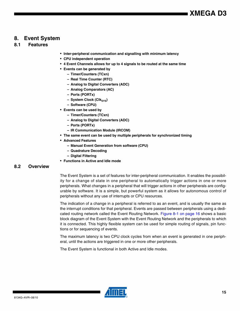
The indication of a change in a peripheral is referred to as an event, and is usually the same asthe interrupt conditions for that peripheral. Events are passed between peripherals using a dedi-cated routing network called the Event Routing Network. Figure 8-1 on page 16 shows a basicblock diagram of the Event System with the Event Routing Network and the peripherals to whichit is connected. This highly flexible system can be used for simple routing of signals, pin func-tions or for sequencing of events.
The maximum latency is two CPU clock cycles from when an event is generated in one periph-eral, until the actions are triggered in one or more other peripherals.
The Event System is functional in both Active and Idle modes.
158134G–AVR–08/10
XMEGA D3
Figure 8-1. Event system block diagram.
The Event Routing Network can directly connect together ADCs, Analog Comparators (AC),I/O ports (PORTx), the Real-time Counter (RTC), Timer/Counters (T/C) and the IR Communica-tion Module (IRCOM). Events can also be generated from software (CPU).
All events from all peripherals are always routed into the Event Routing Network. This consist offour multiplexers where each can be configured in software to select which event to be routedinto that event channel. All four event channels are connected to the peripherals that can useevents, and each of these peripherals can be configured to use events from one or more eventchannels to automatically trigger a software selectable action.
ADCx
Event Routing Network
PORTx
CPU
ACx
RTC
T/CxnIRCOM
ClkSYS
168134G–AVR–08/10
XMEGA D3
9. System Clock and Clock options
9.1 Features
• Fast start-up time• Safe run-time clock switching• Internal Oscillators:
– 32 MHz run-time calibrated RC oscillator– 2 MHz run-time calibrated RC oscillator – 32.768 kHz calibrated RC oscillator– 32 kHz Ultra Low Power (ULP) oscillator
• External clock options– 0.4 - 16 MHz Crystal Oscillator– 32.768 kHz Crystal Oscillator– External clock
• PLL with internal and external clock options with 2 to 31x multiplication• Clock Prescalers with 2 to 2048x division• Fast peripheral clock running at 2 and 4 times the CPU clock speed• Automatic Run-Time Calibration of internal oscillators• Crystal Oscillator failure detection
9.2 Overview
XMEGA D3 has an advanced clock system, supporting a large number of clock sources. It incor-porates both integrated oscillators, external crystal oscillators and resonators. A high frequencyPhase Locked Loop (PLL) and clock prescalers can be controlled from software to generate awide range of clock frequencies from the clock source input.
It is possible to switch between clock sources from software during run-time. After reset thedevice will always start up running from the 2 Mhz internal oscillator.
A calibration feature is available, and can be used for automatic run-time calibration of the inter-nal 2 MHz and 32 MHz oscillators. This reduce frequency drift over voltage and temperature.
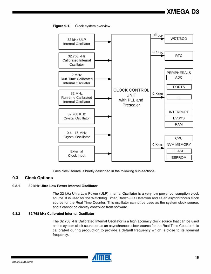
A Crystal Oscillator Failure Monitor can be enabled to issue a Non-Maskable Interrupt andswitch to internal oscillator if the external oscillator fails. Figure 9-1 on page 18 shows the princi-pal clock system in XMEGA D3.
178134G–AVR–08/10
XMEGA D3
Figure 9-1. Clock system overview
Each clock source is briefly described in the following sub-sections.
9.3 Clock Options
9.3.1 32 kHz Ultra Low Power Internal Oscillator
The 32 kHz Ultra Low Power (ULP) Internal Oscillator is a very low power consumption clocksource. It is used for the Watchdog Timer, Brown-Out Detection and as an asynchronous clocksource for the Real Time Counter. This oscillator cannot be used as the system clock source,and it cannot be directly controlled from software.
9.3.2 32.768 kHz Calibrated Internal Oscillator
The 32.768 kHz Calibrated Internal Oscillator is a high accuracy clock source that can be usedas the system clock source or as an asynchronous clock source for the Real Time Counter. It iscalibrated during production to provide a default frequency which is close to its nominalfrequency.
32 MHzRun-time CalibratedInternal Oscillator
32 kHz ULPInternal Oscillator
32.768 kHz Calibrated Internal
Oscillator
32.768 KHz Crystal Oscillator
0.4 - 16 MHzCrystal Oscillator
2 MHzRun-Time Calibrated
Internal Oscillator
ExternalClock Input
CLOCK CONTROL UNIT
with PLL and Prescaler
WDT/BODclkULP
RTCclkRTC
EVSYS
PERIPHERALSADC
PORTS
...clkPER
INTERRUPT
RAM
NVM MEMORY
FLASH
EEPROM
CPU
clkCPU
188134G–AVR–08/10
XMEGA D3
9.3.3 32.768 kHz Crystal Oscillator
The 32.768 kHz Crystal Oscillator is a low power driver for an external watch crystal. It can beused as system clock source or as asynchronous clock source for the Real Time Counter.
9.3.4 0.4 - 16 MHz Crystal Oscillator
The 0.4 - 16 MHz Crystal Oscillator is a driver intended for driving both external resonators andcrystals ranging from 400 kHz to 16 MHz.
9.3.5 2 MHz Run-time Calibrated Internal Oscillator
The 2 MHz Run-time Calibrated Internal Oscillator is a high frequency oscillator. It is calibratedduring production to provide a default frequency which is close to its nominal frequency. Theoscillator can use the 32.768 kHz Calibrated Internal Oscillator or the 32 kHz Crystal Oscillatoras a source for calibrating the frequency run-time to compensate for temperature and voltagedrift hereby optimizing the accuracy of the oscillator.
9.3.6 32 MHz Run-time Calibrated Internal Oscillator
The 32 MHz Run-time Calibrated Internal Oscillator is a high frequency oscillator. It is calibratedduring production to provide a default frequency which is close to its nominal frequency. Theoscillator can use the 32.768 kHz Calibrated Internal Oscillator or the 32 kHz Crystal Oscillatoras a source for calibrating the frequency run-time to compensate for temperature and voltagedrift hereby optimizing the accuracy of the oscillator.
9.3.7 External Clock input
The external clock input gives the possibility to connect a clock from an external source.
9.3.8 PLL with Multiplication factor 2 - 31x
The PLL provides the possibility of multiplying a frequency by any number from 2 to 31. In com-bination with the prescalers, this gives a wide range of output frequencies from all clock sources.
198134G–AVR–08/10
XMEGA D3
10. Power Management and Sleep Modes
10.1 Features
• 5 sleep modes– Idle– Power-down– Power-save– Standby– Extended standby
• Power Reduction registers to disable clocks to unused peripherals
10.2 Overview
The XMEGA D3 provides various sleep modes tailored to reduce power consumption to a mini-mum. All sleep modes are available and can be entered from Active mode. In Active mode theCPU is executing application code. The application code decides when and what sleep mode toenter. Interrupts from enabled peripherals and all enabled reset sources can restore the micro-controller from sleep to Active mode.
In addition, Power Reduction registers provide a method to stop the clock to individual peripher-als from software. When this is done, the current state of the peripheral is frozen and there is nopower consumption from that peripheral. This reduces the power consumption in Active modeand Idle sleep mode.
10.3 Sleep Modes
10.3.1 Idle Mode
In Idle mode the CPU and Non-Volatile Memory are stopped, but all peripherals including theInterrupt Controller and Event System are kept running. Interrupt requests from all enabled inter-rupts will wake the device.
10.3.2 Power-down Mode
In Power-down mode all system clock sources, and the asynchronous Real Time Counter (RTC)clock source, are stopped. This allows operation of asynchronous modules only. The only inter-rupts that can wake up the MCU are the Two Wire Interface address match interrupts, andasynchronous port interrupts, e.g pin change.
10.3.3 Power-save Mode
Power-save mode is identical to Power-down, with one exception: If the RTC is enabled, it willkeep running during sleep and the device can also wake up from RTC interrupts.
10.3.4 Standby Mode
Standby mode is identical to Power-down with the exception that all enabled system clocksources are kept running, while the CPU, Peripheral and RTC clocks are stopped. This reducesthe wake-up time when external crystals or resonators are used.
208134G–AVR–08/10
XMEGA D3
10.3.5 Extended Standby Mode
Extended Standby mode is identical to Power-save mode with the exception that all enabledsystem clock sources are kept running while the CPU and Peripheral clocks are stopped. Thisreduces the wake-up time when external crystals or resonators are used.
218134G–AVR–08/10
XMEGA D3
11. System Control and Reset
11.1 Features
• Multiple reset sources for safe operation and device reset– Power-On Reset – External Reset– Watchdog Reset
The Watchdog Timer runs from separate, dedicated oscillator– Brown-Out Reset
Accurate, programmable Brown-Out levels– PDI reset– Software reset
• Asynchronous reset– No running clock in the device is required for reset
• Reset status register
11.2 Resetting the AVR
During reset, all I/O registers are set to their initial values. The SRAM content is not reset. Appli-cation execution starts from the Reset Vector. The instruction placed at the Reset Vector shouldbe an Absolute Jump (JMP) instruction to the reset handling routine. By default the Reset Vectoraddress is the lowest Flash program memory address, ‘0’, but it is possible to move the ResetVector to the first address in the Boot Section.
The I/O ports of the AVR are immediately tri-stated when a reset source goes active.
The reset functionality is asynchronous, so no running clock is required to reset the device.
After the device is reset, the reset source can be determined by the application by reading theReset Status Register.
11.3 Reset Sources
11.3.1 Power-On Reset
The MCU is reset when the supply voltage VCC is below the Power-on Reset threshold voltage.
11.3.2 External Reset
The MCU is reset when a low level is present on the RESET pin.
11.3.3 Watchdog Reset
The MCU is reset when the Watchdog Timer period expires and the Watchdog Reset is enabled.The Watchdog Timer runs from a dedicated oscillator independent of the System Clock. Formore details see ”WDT - Watchdog Timer” on page 23.
11.3.4 Brown-Out Reset
The MCU is reset when the supply voltage VCC is below the Brown-Out Reset threshold voltageand the Brown-out Detector is enabled. The Brown-out threshold voltage is programmable.
11.3.5 PDI reset
The MCU can be reset through the Program and Debug Interface (PDI).
228134G–AVR–08/10
XMEGA D3
11.3.6 Software reset
The MCU can be reset by the CPU writing to a special I/O register through a timed sequence.
12. WDT - Watchdog Timer
12.1 Features
• 11 selectable timeout periods, from 8 ms to 8s.• Two operation modes
– Standard mode– Window mode
• Runs from the 1 kHz output of the 32 kHz Ultra Low Power oscillator• Configuration lock to prevent unwanted changes
12.2 Overview
The XMEGA D3 has a Watchdog Timer (WDT). The WDT will run continuously when turned onand if the Watchdog Timer is not reset within a software configurable time-out period, the micro-controller will be reset. The Watchdog Reset (WDR) instruction must be run by software to resetthe WDT, and prevent microcontroller reset.
The WDT has a Window mode. In this mode the WDR instruction must be run within a specifiedperiod called a window. Application software can set the minimum and maximum limits for thiswindow. If the WDR instruction is not executed inside the window limits, the microcontroller willbe reset.
A protection mechanism using a timed write sequence is implemented in order to preventunwanted enabling, disabling or change of WDT settings.
For maximum safety, the WDT also has an Always-on mode. This mode is enabled by program-ming a fuse. In Always-on mode, application software can not disable the WDT.
238134G–AVR–08/10
XMEGA D3
13. PMIC - Programmable Multi-level Interrupt Controller
13.1 Features
• Separate interrupt vector for each interrupt• Short, predictable interrupt response time• Programmable Multi-level Interrupt Controller
– 3 programmable interrupt levels– Selectable priority scheme within low level interrupts (round-robin or fixed)– Non-Maskable Interrupts (NMI)
• Interrupt vectors can be moved to the start of the Boot Section
13.2 Overview
XMEGA D3 has a Programmable Multi-level Interrupt Controller (PMIC). All peripherals candefine three different priority levels for interrupts; high, medium or low. Medium level interruptsmay interrupt low level interrupt service routines. High level interrupts may interrupt both low-and medium level interrupt service routines. Low level interrupts have an optional round robinscheme to make sure all interrupts are serviced within a certain amount of time.
The built in oscillator failure detection mechanism can issue a Non-Maskable Interrupt (NMI).
13.3 Interrupt vectors
When an interrupt is serviced, the program counter will jump to the interrupt vector address. Theinterrupt vector is the sum of the peripheral’s base interrupt address and the offset address forspecific interrupts in each peripheral. The base addresses for the XMEGA D3 devices areshown in Table 13-1. Offset addresses for each interrupt available in the peripheral aredescribed for each peripheral in the XMEGA A manual. For peripherals or modules that haveonly one interrupt, the interrupt vector is shown in Table 13-1. The program address is the wordaddress.
Table 13-1. Reset and Interrupt Vectors
Program Address(Base Address) Source Interrupt Description
0x000 RESET
0x002 OSCF_INT_vect Crystal Oscillator Failure Interrupt vector (NMI)
0x004 PORTC_INT_base Port C Interrupt base
0x008 PORTR_INT_base Port R Interrupt base
0x014 RTC_INT_base Real Time Counter Interrupt base
0x018 TWIC_INT_base Two-Wire Interface on Port C Interrupt base
0x01C TCC0_INT_base Timer/Counter 0 on port C Interrupt base
0x028 TCC1_INT_base Timer/Counter 1 on port C Interrupt base
0x030 SPIC_INT_vect SPI on port C Interrupt vector
0x032 USARTC0_INT_base USART 0 on port C Interrupt base
0x040 NVM_INT_base Non-Volatile Memory Interrupt base
0x044 PORTB_INT_base Port B Interrupt base
0x056 PORTE_INT_base Port E INT base
248134G–AVR–08/10
XMEGA D3
0x05A TWIE_INT_base Two-Wire Interface on Port E Interrupt base
0x05E TCE0_INT_base Timer/Counter 0 on port E Interrupt base
0x074 USARTE0_INT_base USART 0 on port E Interrupt base
0x080 PORTD_INT_base Port D Interrupt base
0x084 PORTA_INT_base Port A Interrupt base
0x088 ACA_INT_base Analog Comparator on Port A Interrupt base
0x08E ADCA_INT_base Analog to Digital Converter on Port A Interrupt base
0x09A TCD0_INT_base Timer/Counter 0 on port D Interrupt base
0x0AE SPID_INT_vector SPI D Interrupt vector
0x0B0 USARTD0_INT_base USART 0 on port D Interrupt base
0x0D0 PORTF_INT_base Port F Interrupt base
0x0D8 TCF0_INT_base Timer/Counter 0 on port F Interrupt base
Table 13-1. Reset and Interrupt Vectors (Continued)
Program Address(Base Address) Source Interrupt Description
258134G–AVR–08/10
XMEGA D3
14. I/O Ports
14.1 Features
• Selectable input and output configuration for each pin individually• Flexible pin configuration through dedicated Pin Configuration Register• Synchronous and/or asynchronous input sensing with port interrupts and events
– Sense both edges– Sense rising edges– Sense falling edges– Sense low level
• Asynchronous wake-up from all input sensing configurations• Two port interrupts with flexible pin masking• Highly configurable output driver and pull settings:
– Totem-pole– Pull-up/-down– Wired-AND– Wired-OR– Bus-keeper– Inverted I/O
• Optional Slew rate control• Configuration of multiple pins in a single operation• Read-Modify-Write (RMW) support• Toggle/clear/set registers for Output and Direction registers• Clock output on port pin• Event Channel 0 output on port pin 7• Mapping of port registers (virtual ports) into bit accessible I/O memory space
14.2 Overview
The XMEGA D3 devices have flexible General Purpose I/O Ports. A port consists of up to 8 pins,ranging from pin 0 to pin 7. The ports implement several functions, including synchronous/asyn-chronous input sensing, pin change interrupts and configurable output settings. All functions areindividual per pin, but several pins may be configured in a single operation.
14.3 I/O configuration
All port pins (Pn) have programmable output configuration. In addition, all port pins have aninverted I/O function. For an input, this means inverting the signal between the port pin and thepin register. For an output, this means inverting the output signal between the port register andthe port pin. The inverted I/O function can be used also when the pin is used for alternatefunctions.
268134G–AVR–08/10
XMEGA D3
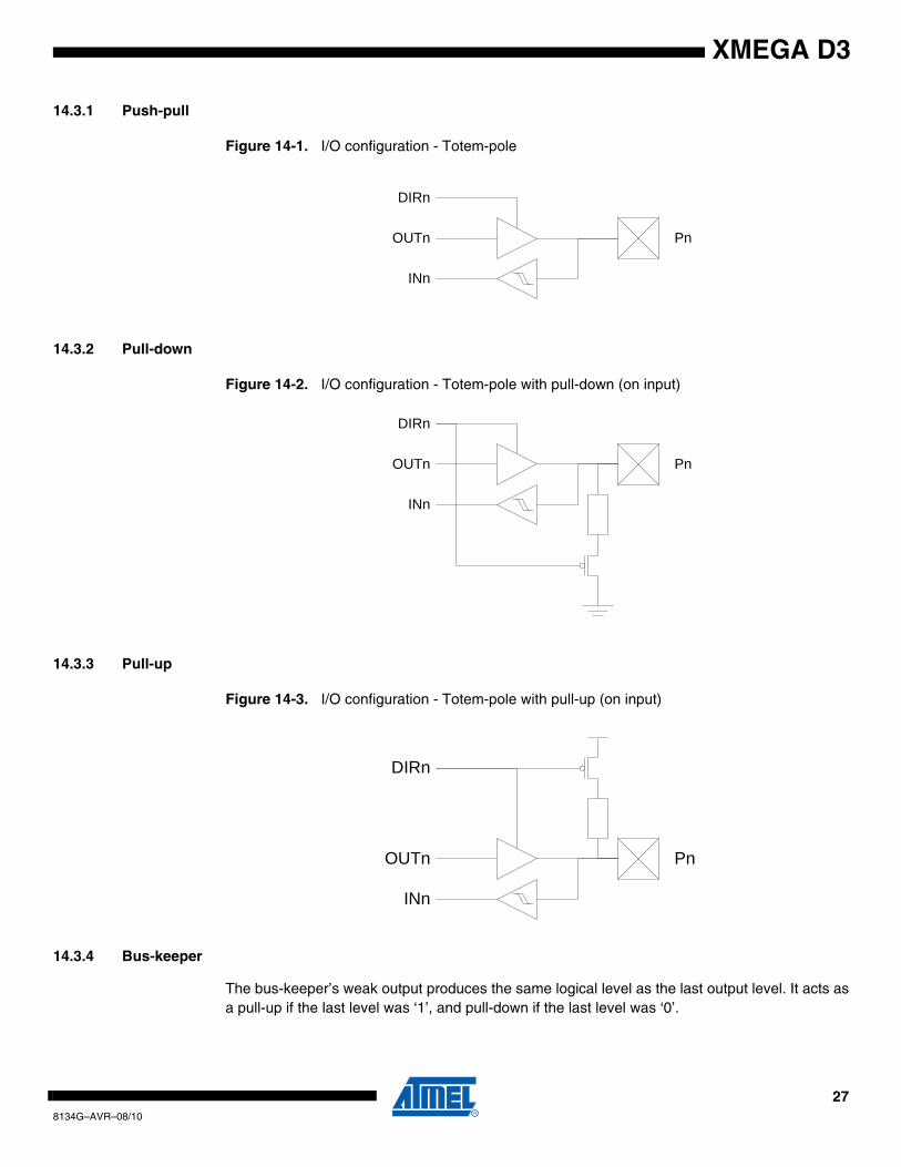
14.3.1 Push-pull
Figure 14-1. I/O configuration - Totem-pole
14.3.2 Pull-down
Figure 14-2. I/O configuration - Totem-pole with pull-down (on input)
14.3.3 Pull-up
Figure 14-3. I/O configuration - Totem-pole with pull-up (on input)
14.3.4 Bus-keeper
The bus-keeper’s weak output produces the same logical level as the last output level. It acts asa pull-up if the last level was ‘1’, and pull-down if the last level was ‘0’.
INn
OUTn
DIRn
Pn
INn
OUTn
DIRn
Pn
INn
OUTn
DIRn
Pn
278134G–AVR–08/10
XMEGA D3
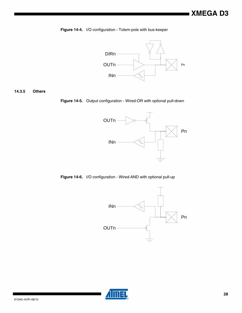
Figure 14-4. I/O configuration - Totem-pole with bus-keeper
14.3.5 Others
Figure 14-5. Output configuration - Wired-OR with optional pull-down
Figure 14-6. I/O configuration - Wired-AND with optional pull-up
INn
OUTn
DIRn
Pn
INn
OUTn
Pn
INn
OUTn
Pn
288134G–AVR–08/10
XMEGA D3
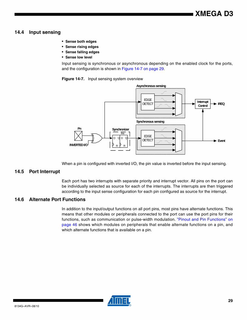
14.4 Input sensing
• Sense both edges• Sense rising edges• Sense falling edges• Sense low level
Input sensing is synchronous or asynchronous depending on the enabled clock for the ports,and the configuration is shown in Figure 14-7 on page 29.
Figure 14-7. Input sensing system overview
When a pin is configured with inverted I/O, the pin value is inverted before the input sensing.
14.5 Port Interrupt
Each port has two interrupts with separate priority and interrupt vector. All pins on the port canbe individually selected as source for each of the interrupts. The interrupts are then triggeredaccording to the input sense configuration for each pin configured as source for the interrupt.
14.6 Alternate Port Functions
In addition to the input/output functions on all port pins, most pins have alternate functions. Thismeans that other modules or peripherals connected to the port can use the port pins for theirfunctions, such as communication or pulse-width modulation. ”Pinout and Pin Functions” onpage 46 shows which modules on peripherals that enable alternate functions on a pin, andwhich alternate functions that is available on a pin.
INVERTED I/O
Interrupt Control IREQ
Event
Pn
D Q
R
D Q
R
SynchronizerINn
EDGE DETECT
Asynchronous sensing
Synchronous sensing
EDGE DETECT
298134G–AVR–08/10
XMEGA D3
15. T/C - 16-bits Timer/Counter with PWM
15.1 Features
• Five 16-bit Timer/Counters– Four Timer/Counters of type 0– One Timer/Counters of type 1
• Four Compare or Capture (CC) Channels in Timer/Counter 0• Two Compare or Capture (CC) Channels in Timer/Counter 1• Double Buffered Timer Period Setting• Double Buffered Compare or Capture Channels• Waveform Generation:
– Single Slope Pulse Width Modulation– Dual Slope Pulse Width Modulation– Frequency Generation
• Input Capture:– Input Capture with Noise Cancelling– Frequency capture – Pulse width capture– 32-bit input capture
• Event Counter with Direction Control• Timer Overflow and Timer Error Interrupts and Events• One Compare Match or Capture Interrupt and Event per CC Channel• Hi-Resolution Extension (Hi-Res)• Advanced Waveform Extension (AWEX)
15.2 Overview
XMEGA D3 has five Timer/Counters, four Timer/Counter 0 and one Timer/Counter 1. The differ-ence between them is that Timer/Counter 0 has four Compare/Capture channels, whileTimer/Counter 1 has two Compare/Capture channels.
The Timer/Counters (T/C) are 16-bit and can count any clock, event or external input in themicrocontroller. A programmable prescaler is available to get a useful T/C resolution. Updates ofTimer and Compare registers are double buffered to ensure glitch free operation. Single slopePWM, dual slope PWM and frequency generation waveforms can be generated using the Com-pare Channels.
Through the Event System, any input pin or event in the microcontroller can be used to triggerinput capture, hence no dedicated pins are required for this. The input capture has a noise can-celler to avoid incorrect capture of the T/C, and can be used to do frequency and pulse widthmeasurements.
A wide range of interrupt or event sources are available, including T/C Overflow, Comparematch and Capture for each Compare/Capture channel in the T/C.
PORTC has one Timer/Counter 0 and one Timer/Counter1. PORTD, PORTE and PORTF eachhave one Timer/Counter 0. Notation of these are TCC0 (Time/Counter C0), TCC1, TCD0, TCE0,and TCF0, respectively.
308134G–AVR–08/10
XMEGA D3
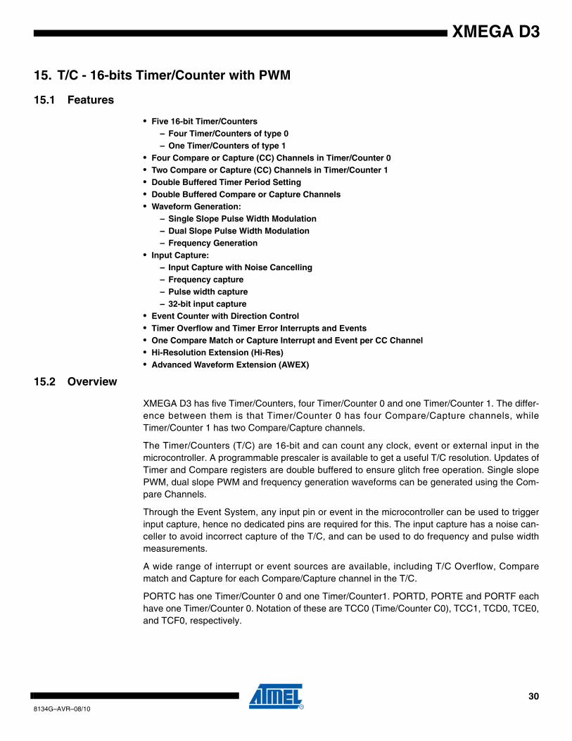
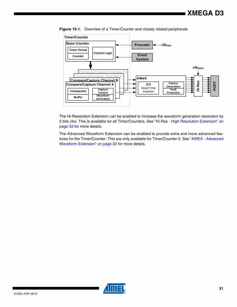
Figure 15-1. Overview of a Timer/Counter and closely related peripherals
The Hi-Resolution Extension can be enabled to increase the waveform generation resolution by2 bits (4x). This is available for all Timer/Counters. See ”Hi-Res - High Resolution Extension” onpage 33 for more details.
The Advanced Waveform Extension can be enabled to provide extra and more advanced fea-tures for the Timer/Counter. This are only available for Timer/Counter 0. See ”AWEX - AdvancedWaveform Extension” on page 32 for more details.
AWeX
Compare/Capture Channel DCompare/Capture Channel C
Compare/Capture Channel BCompare/Capture Channel A
Waveform GenerationBuffer
Comparator Hi-R
es
Fault Protection
Capture Control
Base Counter
CounterControl Logic
Timer PeriodPrescaler
DTIDead-Time
Insertion
Pattern Generation
clkPER4
POR
T
Event System
clkPER
Timer/Counter
318134G–AVR–08/10
XMEGA D3
16. AWEX - Advanced Waveform Extension
16.1 Features
• Output with complementary output from each Capture channel• Four Dead Time Insertion (DTI) Units, one for each Capture channel• 8-bit DTI Resolution• Separate High and Low Side Dead-Time Setting• Double Buffered Dead-Time• Event Controlled Fault Protection• Single Channel Multiple Output Operation (for BLDC motor control)• Double Buffered Pattern Generation
16.2 Overview
The Advanced Waveform Extension (AWEX) provides extra features to the Timer/Counter inWaveform Generation (WG) modes. The AWEX enables easy and safe implementation of forexample, advanced motor control (AC, BLDC, SR, and Stepper) and power control applications.
Any WG output from a Timer/Counter 0 is split into a complimentary pair of outputs when anyAWEX feature is enabled. These output pairs go through a Dead-Time Insertion (DTI) unit thatenables generation of the non-inverted Low Side (LS) and inverted High Side (HS) of the WGoutput with dead time insertion between LS and HS switching. The DTI output will override thenormal port value according to the port override setting. Optionally the final output can beinverted by using the invert I/O setting for the port pin.
The Pattern Generation unit can be used to generate a synchronized bit pattern on the port it isconnected to. In addition, the waveform generator output from Compare Channel A can be dis-tributed to, and override all port pins. When the Pattern Generator unit is enabled, the DTI unit isbypassed.
The Fault Protection unit is connected to the Event System. This enables any event to trigger afault condition that will disable the AWEX output. Several event channels can be used to triggerfault on several different conditions.
The AWEX is available for TCC0. The notation of this is AWEXC.
328134G–AVR–08/10
XMEGA D3
17. Hi-Res - High Resolution Extension
17.1 Features• Increases Waveform Generator resolution by 2-bits (4x)• Supports Frequency, single- and dual-slope PWM operation• Supports the AWEX when this is enabled and used for the same Timer/Counter
17.2 OverviewThe Hi-Resolution (Hi-Res) Extension is able to increase the resolution of the waveform genera-tion output by a factor of 4. When enabled for a Timer/Counter, the Fast Peripheral clock runningat four times the CPU clock speed will be as input to the Timer/Counter.
The High Resolution Extension can also be used when an AWEX is enabled and used with aTimer/Counter.
XMEGA D3 devices have one Hi-Res Extension that can be enabled for each Timer/Counterson PORTC. The notation of this is HIRESC.
338134G–AVR–08/10
XMEGA D3
18. RTC - Real-Time Counter
18.1 Features
• 16-bit Timer• Flexible Tick resolution ranging from 1 Hz to 32.768 kHz• One Compare register• One Period register• Clear timer on Overflow or Compare Match• Overflow or Compare Match event and interrupt generation
18.2 Overview
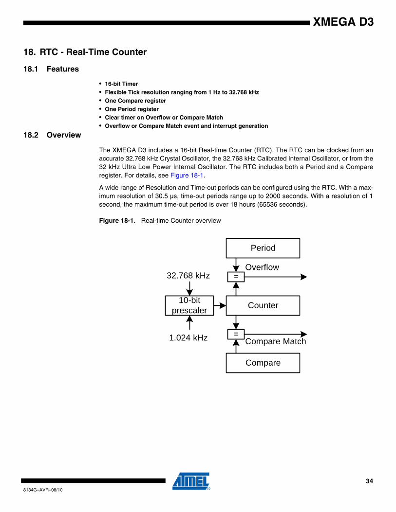
The XMEGA D3 includes a 16-bit Real-time Counter (RTC). The RTC can be clocked from anaccurate 32.768 kHz Crystal Oscillator, the 32.768 kHz Calibrated Internal Oscillator, or from the32 kHz Ultra Low Power Internal Oscillator. The RTC includes both a Period and a Compareregister. For details, see Figure 18-1.
A wide range of Resolution and Time-out periods can be configured using the RTC. With a max-imum resolution of 30.5 µs, time-out periods range up to 2000 seconds. With a resolution of 1second, the maximum time-out period is over 18 hours (65536 seconds).
Figure 18-1. Real-time Counter overview
10-bit prescaler Counter
Period
Compare
=
=
Overflow
Compare Match1.024 kHz
32.768 kHz
348134G–AVR–08/10
XMEGA D3
19. TWI - Two Wire Interface
19.1 Features
• Two Identical TWI peripherals• Simple yet Powerful and Flexible Communication Interface• Both Master and Slave Operation Supported• Device can Operate as Transmitter or Receiver• 7-bit Address Space Allows up to 128 Different Slave Addresses• Multi-master Arbitration Support• Up to 400 kHz Data Transfer Speed• Slew-rate Limited Output Drivers• Noise Suppression Circuitry Rejects Spikes on Bus Lines• Fully Programmable Slave Address with General Call Support• Address Recognition Causes Wake-up when in Sleep Mode• I2C and System Management Bus (SMBus) compatible
19.2 Overview
The Two-Wire Interface (TWI) is a bi-directional wired-AND bus with only two lines, the clock(SCL) line and the data (SDA) line. The protocol makes it possible to interconnect up to 128 indi-vidually addressable devices. Since it is a multi-master bus, one or more devices capable oftaking control of the bus can be connected.
The only external hardware needed to implement the bus is a single pull-up resistor for each ofthe TWI bus lines. Mechanisms for resolving bus contention are inherent in the TWI protocol.
PORTC and PORTE each has one TWI. Notation of these peripherals are TWIC and TWIE,respectively.
358134G–AVR–08/10
XMEGA D3
20. SPI - Serial Peripheral Interface
20.1 Features
• Two Identical SPI peripherals• Full-duplex, Three-wire Synchronous Data Transfer• Master or Slave Operation• LSB First or MSB First Data Transfer• Seven Programmable Bit Rates• End of Transmission Interrupt Flag• Write Collision Flag Protection• Wake-up from Idle Mode• Double Speed (CK/2) Master SPI Mode
20.2 Overview
The Serial Peripheral Interface (SPI) allows high-speed full-duplex, synchronous data transferbetween different devices. Devices can communicate using a master-slave scheme, and data istransferred both to and from the devices simultaneously.
PORTC and PORTD each has one SPI. Notation of these peripherals are SPIC and SPID,respectively.
368134G–AVR–08/10
XMEGA D3
21. USART
21.1 Features
• Three Identical USART peripherals• Full Duplex Operation (Independent Serial Receive and Transmit Registers)• Asynchronous or Synchronous Operation• Master or Slave Clocked Synchronous Operation• High-resolution Arithmetic Baud Rate Generator• Supports Serial Frames with 5, 6, 7, 8, or 9 Data Bits and 1 or 2 Stop Bits• Odd or Even Parity Generation and Parity Check Supported by Hardware• Data OverRun Detection• Framing Error Detection• Noise Filtering Includes False Start Bit Detection and Digital Low Pass Filter• Three Separate Interrupts on TX Complete, TX Data Register Empty and RX Complete• Multi-processor Communication Mode• Double Speed Asynchronous Communication Mode• Master SPI mode for SPI communication• IrDA support through the IRCOM module
21.2 Overview
The Universal Synchronous and Asynchronous serial Receiver and Transmitter (USART) is ahighly flexible serial communication module. The USART supports full duplex communication,and both asynchronous and clocked synchronous operation. The USART can also be set inMaster SPI mode to be used for SPI communication.
Communication is frame based, and the frame format can be customized to support a widerange of standards. The USART is buffered in both direction, enabling continued data transmis-sion without any delay between frames. There are separate interrupt vectors for receive andtransmit complete, enabling fully interrupt driven communication. Frame error and buffer over-flow are detected in hardware and indicated with separate status flags. Even or odd paritygeneration and parity check can also be enabled.
One USART can use the IRCOM module to support IrDA 1.4 physical compliant pulse modula-tion and demodulation for baud rates up to 115.2 kbps.
PORTC, PORTD, and PORTE each has one USART. Notation of these peripherals areUSARTC0, USARTD0 and USARTE0, respectively.
378134G–AVR–08/10
XMEGA D3
22. IRCOM - IR Communication Module
22.1 Features
• Pulse modulation/demodulation for infrared communication• Compatible to IrDA 1.4 physical for baud rates up to 115.2 kbps• Selectable pulse modulation scheme
– 3/16 of baud rate period– Fixed pulse period, 8-bit programmable– Pulse modulation disabled
• Built in filtering• Can be connected to and used by one USART at the time
22.2 Overview
XMEGA contains an Infrared Communication Module (IRCOM) for IrDA communication withbaud rates up to 115.2 kbps. This supports three modulation schemes: 3/16 of baud rate period,fixed programmable pulse time based on the Peripheral Clock speed, or pulse modulation dis-abled. There is one IRCOM available which can be connected to any USART to enable infraredpulse coding/decoding for that USART.
388134G–AVR–08/10
XMEGA D3
23. ADC - 12-bit Analog to Digital Converter
23.1 Features
• One ADC with 12-bit resolution• 200 ksps sample rate• Signed and Unsigned conversions• 16 single ended inputs• 8x4 differential inputs• 3 internal inputs:
– Integrated Temperature Sensor– VCC voltage divided by 10– Bandgap voltage
• Software selectable gain of 1, 2, 4, 8, 16, 32 or 64• Software selectable resolution of 8- or 12-bit.• Internal or External Reference selection• Event triggered conversion for accurate timing• Interrupt/Event on compare result
23.2 Overview
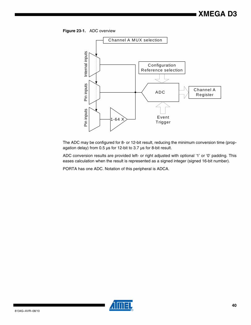
XMEGA D3 devices have one Analog to Digital Converters (ADC), see Figure 23-1 on page 40.
The ADC converts analog voltages to digital values. The ADC has 12-bit resolution and iscapable of converting up to 200K samples per second. The input selection is flexible, and bothsingleended and differential measurements can be done. For differential measurements anoptional gain stage is available to increase the dynamic range. In addition several internal signalinputs are available. The ADC can provide both signed and unsigned results.
ADC measurements can either be started by application software or an incoming event fromanother peripheral in the device. The latter ensure the ADC measurements can be started withpredictable timing, and without software intervention. The ADC has one channel, meaning thereis one input selection (MUX selection) and one result register available.
Both internal and external analog reference voltages can be used. A very accurate internal1.00V reference is available.
An integrated temperature sensor is available and the output from this can be measured with theADC. A VCC/10 signal and the Bandgap voltage can also be measured by the ADC.
398134G–AVR–08/10
XMEGA D3
Figure 23-1. ADC overview
The ADC may be configured for 8- or 12-bit result, reducing the minimum conversion time (prop-agation delay) from 0.5 µs for 12-bit to 3.7 µs for 8-bit result.
ADC conversion results are provided left- or right adjusted with optional ‘1’ or ‘0’ padding. Thiseases calculation when the result is represented as a signed integer (signed 16-bit number).
PORTA has one ADC. Notation of this peripheral is ADCA.
ADC Channel A Register
Pin
inpu
tsP
in in
puts
1-64 X
Inte
rnal
inpu
ts
Channel A MUX selection
Event Trigger
ConfigurationReference selection
408134G–AVR–08/10
XMEGA D3
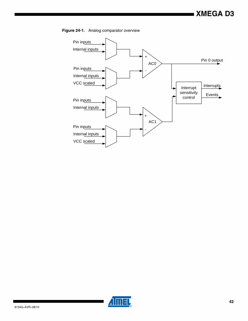
24. AC - Analog Comparator
24.1 Features
• Two Analog Comparators• Selectable hysteresis
– No, Small or Large• Analog Comparator output available on pin• Flexible Input Selection
– All pins on the port– Bandgap reference voltage.– Voltage scaler that can perform a 64-level scaling of the internal VCC voltage.
• Interrupt and event generation on– Rising edge– Falling edge– Toggle
• Window function interrupt and event generation on– Signal above window– Signal inside window– Signal below window
24.2 Overview
XMEGA D3 features two Analog Comparators (AC). An Analog Comparator compares two volt-ages, and the output indicates which input is largest. The Analog Comparator may be configuredto give interrupt requests and/or events upon several different combinations of input change.
Hysteresis can be adjusted in order to find the optimal operation for each application.
A wide range of input selection is available, both external pins and several internal signals canbe used.
The Analog Comparators are always grouped in pairs (AC0 and AC1) on each analog port. Theyhave identical behavior but separate control registers.
Optionally, the state of the comparator is directly available on a pin.
PORTA and has one AC pair. Notations of this peripheral is ACA.
418134G–AVR–08/10
XMEGA D3
Figure 24-1. Analog comparator overview
AC0
+
-
Pin inputs
Internal inputs
Pin inputs
Internal inputs
VCC scaledInterrupt
sensitivity control
Interrupts
AC1+
-
Pin inputs
Internal inputs
Pin inputs
Internal inputs
VCC scaled
Events
Pin 0 output
428134G–AVR–08/10
XMEGA D3
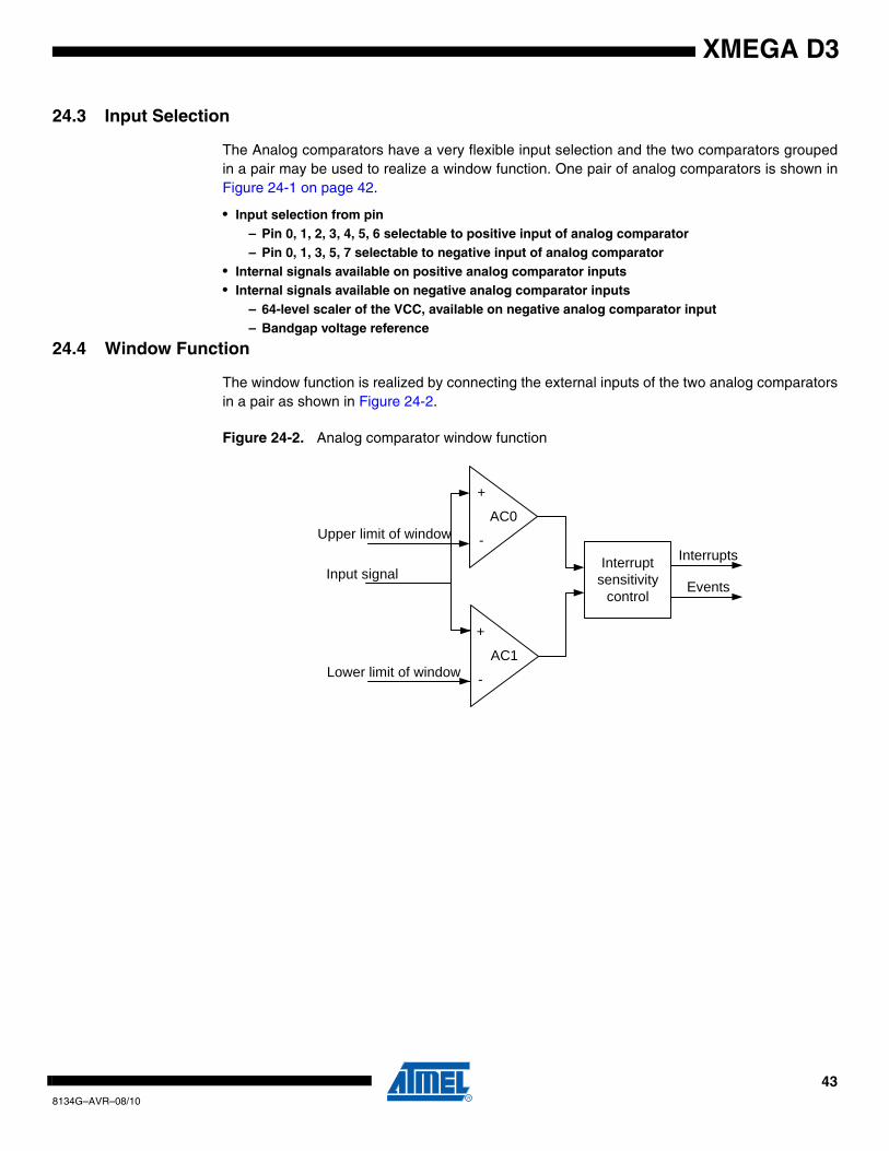
24.3 Input Selection
The Analog comparators have a very flexible input selection and the two comparators groupedin a pair may be used to realize a window function. One pair of analog comparators is shown inFigure 24-1 on page 42.
• Input selection from pin– Pin 0, 1, 2, 3, 4, 5, 6 selectable to positive input of analog comparator– Pin 0, 1, 3, 5, 7 selectable to negative input of analog comparator
• Internal signals available on positive analog comparator inputs• Internal signals available on negative analog comparator inputs
– 64-level scaler of the VCC, available on negative analog comparator input– Bandgap voltage reference
24.4 Window Function
The window function is realized by connecting the external inputs of the two analog comparatorsin a pair as shown in Figure 24-2.
Figure 24-2. Analog comparator window function
AC0
+
-
AC1
+
-
Input signal
Upper limit of window
Lower limit of window
Interrupt sensitivity
control
Interrupts
Events
438134G–AVR–08/10
XMEGA D3
25. OCD - On-chip Debug
25.1 Features
• Complete Program Flow Control– Go, Stop, Reset, Step into, Step over, Step out, Run-to-Cursor
• Debugging on C and high-level language source code level• Debugging on Assembler and disassembler level • 1 dedicated program address or source level breakpoint for AVR Studio / debugger• 4 Hardware Breakpoints• Unlimited Number of User Program Breakpoints• Unlimited Number of User Data Breakpoints, with break on:
– Data location read, write or both read and write– Data location content equal or not equal to a value– Data location content is greater or less than a value– Data location content is within or outside a range– Bits of a data location are equal or not equal to a value
• Non-Intrusive Operation– No hardware or software resources in the device are used
• High Speed Operation– No limitation on debug/programming clock frequency versus system clock frequency
25.2 Overview
The XMEGA D3 has a powerful On-Chip Debug (OCD) system that - in combination with Atmel’sdevelopment tools - provides all the necessary functions to debug an application. It has supportfor program and data breakpoints, and can debug an application from C and high level languagesource code level, as well as assembler and disassembler level. It has full Non-Intrusive Opera-tion and no hardware or software resources in the device are used. The ODC system isaccessed through an external debugging tool which connects to the PDI interface. Refer to ”PDI- Program and Debug Interface” on page 45.
448134G–AVR–08/10
XMEGA D3
26. PDI - Program and Debug Interface
26.1 Features
• PDI - Program and Debug Interface (Atmel proprietary 2-pin interface)• Access to the OCD system• Programming of Flash, EEPROM, Fuses and Lock Bits
26.2 Overview
The programming and debug facilities are accessed through the PDI interface. The PDI physicalinterface uses one dedicated pin together with the Reset pin, and no general purpose pins areused.
The PDI is an Atmel proprietary protocol for communication between the microcontroller andAtmel’s or third party development tools.
458134G–AVR–08/10
XMEGA D3
27. Pinout and Pin Functions
The pinout of XMEGA D3 is shown in ”” on page 2. In addition to general I/O functionality, eachpin may have several function. This will depend on which peripheral is enabled and connected tothe actual pin. Only one of the alternate pin functions can be used at time.
27.1 Alternate Pin Function DescriptionThe tables below show the notation for all pin functions available and describe its function.
27.1.1 Operation/Power Supply
27.1.2 Port Interrupt functions
27.1.3 Analog functions
27.1.4 Timer/Counter and AWEX functions
VCC Digital supply voltage
AVCC Analog supply voltage
GND Ground
SYNC Port pin with full synchronous and limited asynchronous interrupt function
ASYNC Port pin with full synchronous and full asynchronous interrupt function
ACn Analog Comparator input pin n
AC0OUT Analog Comparator 0 Output
ADCn Analog to Digital Converter input pin n
AREF Analog Reference input pin
OCnx Output Compare Channel x for Timer/Counter n
OCnx Inverted Output Compare Channel x for Timer/Counter n
OCnxLS Output Compare Channel x Low Side for Timer/Counter n
OCnxHS Output Compare Channel x High Side for Timer/Counter n
468134G–AVR–08/10
XMEGA D3
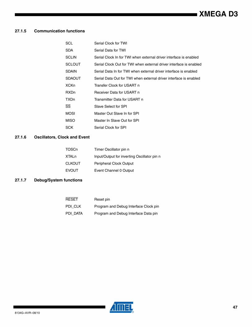
27.1.5 Communication functions
27.1.6 Oscillators, Clock and Event
27.1.7 Debug/System functions
SCL Serial Clock for TWI
SDA Serial Data for TWI
SCLIN Serial Clock In for TWI when external driver interface is enabled
SCLOUT Serial Clock Out for TWI when external driver interface is enabled
SDAIN Serial Data In for TWI when external driver interface is enabled
SDAOUT Serial Data Out for TWI when external driver interface is enabled
XCKn Transfer Clock for USART n
RXDn Receiver Data for USART n
TXDn Transmitter Data for USART n
SS Slave Select for SPI
MOSI Master Out Slave In for SPI
MISO Master In Slave Out for SPI
SCK Serial Clock for SPI
TOSCn Timer Oscillator pin n
XTALn Input/Output for inverting Oscillator pin n
CLKOUT Peripheral Clock Output
EVOUT Event Channel 0 Output
RESET Reset pin
PDI_CLK Program and Debug Interface Clock pin
PDI_DATA Program and Debug Interface Data pin
478134G–AVR–08/10
XMEGA D3
27.2 Alternate Pin FunctionsThe tables below show the main and alternate pin functions for all pins on each port. They alsoshow which peripheral that makes use of or enables the alternate pin function.
Table 27-1. Port A - Alternate functions
PORT A PIN # INTERRUPT ADCA POS ADCA NEGADAA
GAINPOSADCA
GAINNEG ACA POS ACA NEG ACA OUT REFA
GND 60
AVCC 61
PA0 62 SYNC ADC0 ADC0 ADC0 AC0 AC0 AREFA
PA1 63 SYNC ADC1 ADC1 ADC1 AC1 AC1
PA2 64 SYNC/ASYNC ADC2 ADC2 ADC2 AC2
PA3 1 SYNC ADC3 ADC3 ADC3 AC3 AC3
PA4 2 SYNC ADC4 ADC4 ADC4 AC4
PA5 3 SYNC ADC5 ADC5 ADC5 AC5 AC5
PA6 4 SYNC ADC6 ADC6 ADC6 AC6
PA7 5 SYNC ADC7 ADC7 ADC7 AC7 AC0 OUT
Table 27-2. Port B - Alternate functions
PORT B PIN # INTERRUPT ADCA POS REFB
PB0 6 SYNC ADC8 AREFB
PB1 6 SYNC ADC9
PB2 8 SYNC/ASYNC ADC10
PB3 9 SYNC ADC11
PB4 10 SYNC ADC12
PB5 11 SYNC ADC13
PB6 12 SYNC ADC14
PB7 13 SYNC ADC15
GND 14
VCC 15
488134G–AVR–08/10
XMEGA D3
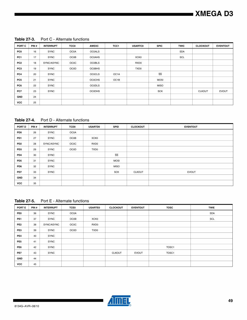
Table 27-3. Port C - Alternate functions
PORT C PIN # INTERRUPT TCC0 AWEXC TCC1 USARTC0 SPIC TWIC CLOCKOUT EVENTOUT
PC0 16 SYNC OC0A OC0ALS SDA
PC1 17 SYNC OC0B OC0AHS XCK0 SCL
PC2 18 SYNC/ASYNC OC0C OC0BLS RXD0
PC3 19 SYNC OC0D OC0BHS TXD0
PC4 20 SYNC OC0CLS OC1A SS
PC5 21 SYNC OC0CHS OC1B MOSI
PC6 22 SYNC OC0DLS MISO
PC7 23 SYNC OC0DHS SCK CLKOUT EVOUT
GND 24
VCC 25
Table 27-4. Port D - Alternate functions
PORT D PIN # INTERRUPT TCD0 USARTD0 SPID CLOCKOUT EVENTOUT
PD0 26 SYNC OC0A
PD1 27 SYNC OC0B XCK0
PD2 28 SYNC/ASYNC OC0C RXD0
PD3 29 SYNC OC0D TXD0
PD4 30 SYNC SS
PD5 31 SYNC MOSI
PD6 32 SYNC MISO
PD7 33 SYNC SCK CLKOUT EVOUT
GND 34
VCC 35
Table 27-5. Port E - Alternate functions
PORT E PIN # INTERRUPT TCE0 USARTE0 CLOCKOUT EVENTOUT TOSC TWIE
PE0 36 SYNC OC0A SDA
PE1 37 SYNC OC0B XCK0 SCL
PE2 38 SYNC/ASYNC OC0C RXD0
PE3 39 SYNC OC0D TXD0
PE4 40 SYNC
PE5 41 SYNC
PE6 42 SYNC TOSC1
PE7 43 SYNC CLKOUT EVOUT TOSC1
GND 44
VCC 45
498134G–AVR–08/10
XMEGA D3
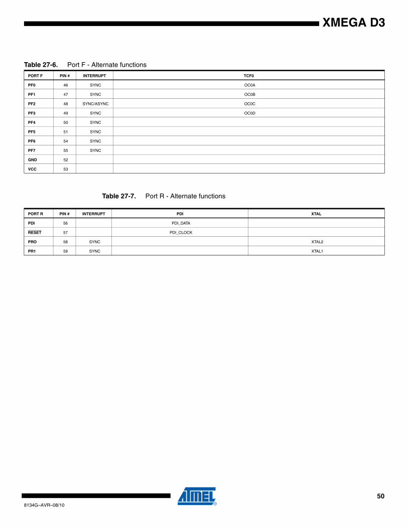
Table 27-7. Port R - Alternate functions
Table 27-6. Port F - Alternate functions
PORT F PIN # INTERRUPT TCF0
PF0 46 SYNC OC0A
PF1 47 SYNC OC0B
PF2 48 SYNC/ASYNC OC0C
PF3 49 SYNC OC0D
PF4 50 SYNC
PF5 51 SYNC
PF6 54 SYNC
PF7 55 SYNC
GND 52
VCC 53
PORT R PIN # INTERRUPT PDI XTAL
PDI 56 PDI_DATA
RESET 57 PDI_CLOCK
PRO 58 SYNC XTAL2
PR1 59 SYNC XTAL1
508134G–AVR–08/10
XMEGA D3
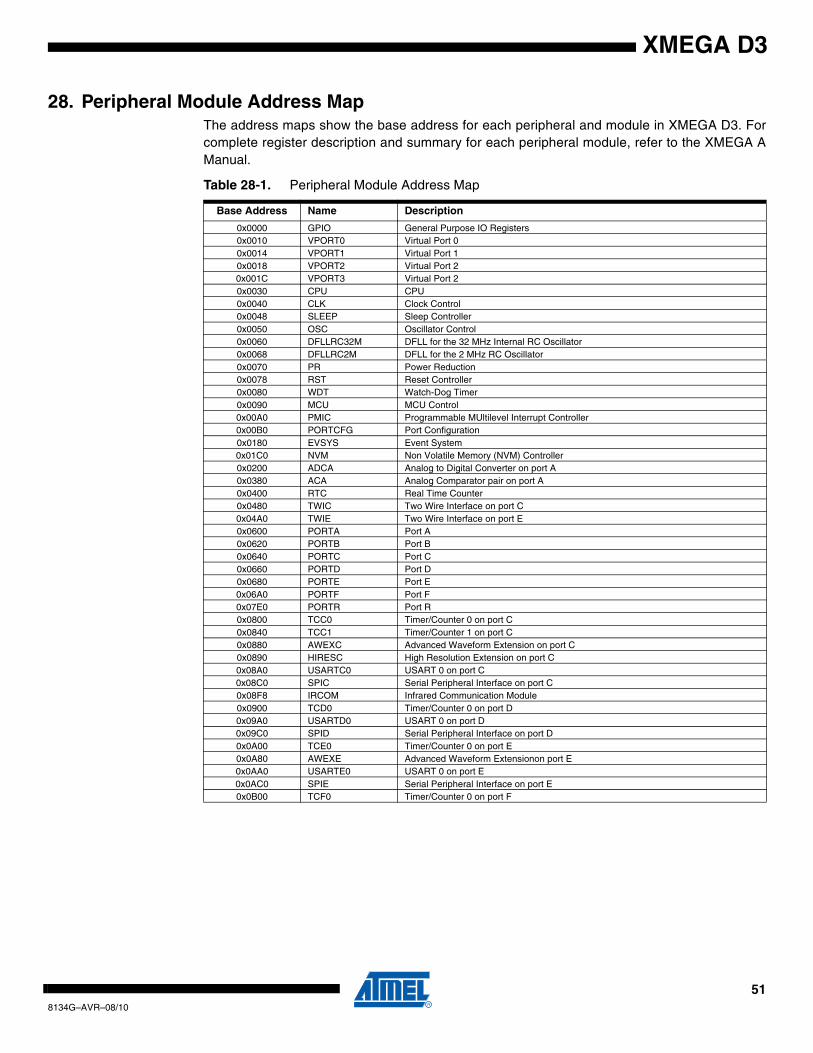
28. Peripheral Module Address MapThe address maps show the base address for each peripheral and module in XMEGA D3. Forcomplete register description and summary for each peripheral module, refer to the XMEGA AManual.
Table 28-1. Peripheral Module Address Map
Base Address Name Description
0x0000 GPIO General Purpose IO Registers0x0010 VPORT0 Virtual Port 00x0014 VPORT1 Virtual Port 10x0018 VPORT2 Virtual Port 20x001C VPORT3 Virtual Port 20x0030 CPU CPU0x0040 CLK Clock Control0x0048 SLEEP Sleep Controller0x0050 OSC Oscillator Control0x0060 DFLLRC32M DFLL for the 32 MHz Internal RC Oscillator0x0068 DFLLRC2M DFLL for the 2 MHz RC Oscillator0x0070 PR Power Reduction0x0078 RST Reset Controller0x0080 WDT Watch-Dog Timer0x0090 MCU MCU Control0x00A0 PMIC Programmable MUltilevel Interrupt Controller0x00B0 PORTCFG Port Configuration0x0180 EVSYS Event System0x01C0 NVM Non Volatile Memory (NVM) Controller0x0200 ADCA Analog to Digital Converter on port A0x0380 ACA Analog Comparator pair on port A0x0400 RTC Real Time Counter0x0480 TWIC Two Wire Interface on port C0x04A0 TWIE Two Wire Interface on port E0x0600 PORTA Port A0x0620 PORTB Port B0x0640 PORTC Port C0x0660 PORTD Port D0x0680 PORTE Port E0x06A0 PORTF Port F0x07E0 PORTR Port R0x0800 TCC0 Timer/Counter 0 on port C0x0840 TCC1 Timer/Counter 1 on port C0x0880 AWEXC Advanced Waveform Extension on port C0x0890 HIRESC High Resolution Extension on port C0x08A0 USARTC0 USART 0 on port C0x08C0 SPIC Serial Peripheral Interface on port C0x08F8 IRCOM Infrared Communication Module0x0900 TCD0 Timer/Counter 0 on port D0x09A0 USARTD0 USART 0 on port D0x09C0 SPID Serial Peripheral Interface on port D0x0A00 TCE0 Timer/Counter 0 on port E0x0A80 AWEXE Advanced Waveform Extensionon port E0x0AA0 USARTE0 USART 0 on port E0x0AC0 SPIE Serial Peripheral Interface on port E0x0B00 TCF0 Timer/Counter 0 on port F
518134G–AVR–08/10
XMEGA D3
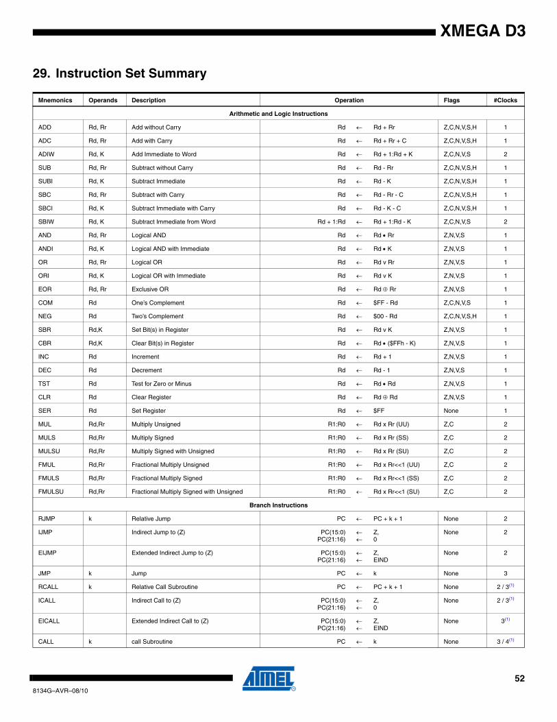
29. Instruction Set Summary
Mnemonics Operands Description Operation Flags #Clocks
Arithmetic and Logic Instructions
ADD Rd, Rr Add without Carry Rd ← Rd + Rr Z,C,N,V,S,H 1
ADC Rd, Rr Add with Carry Rd ← Rd + Rr + C Z,C,N,V,S,H 1
ADIW Rd, K Add Immediate to Word Rd ← Rd + 1:Rd + K Z,C,N,V,S 2
SUB Rd, Rr Subtract without Carry Rd ← Rd - Rr Z,C,N,V,S,H 1
SUBI Rd, K Subtract Immediate Rd ← Rd - K Z,C,N,V,S,H 1
SBC Rd, Rr Subtract with Carry Rd ← Rd - Rr - C Z,C,N,V,S,H 1
SBCI Rd, K Subtract Immediate with Carry Rd ← Rd - K - C Z,C,N,V,S,H 1
SBIW Rd, K Subtract Immediate from Word Rd + 1:Rd ← Rd + 1:Rd - K Z,C,N,V,S 2
AND Rd, Rr Logical AND Rd ← Rd • Rr Z,N,V,S 1
ANDI Rd, K Logical AND with Immediate Rd ← Rd • K Z,N,V,S 1
OR Rd, Rr Logical OR Rd ← Rd v Rr Z,N,V,S 1
ORI Rd, K Logical OR with Immediate Rd ← Rd v K Z,N,V,S 1
EOR Rd, Rr Exclusive OR Rd ← Rd ⊕ Rr Z,N,V,S 1
COM Rd One’s Complement Rd ← $FF - Rd Z,C,N,V,S 1
NEG Rd Two’s Complement Rd ← $00 - Rd Z,C,N,V,S,H 1
SBR Rd,K Set Bit(s) in Register Rd ← Rd v K Z,N,V,S 1
CBR Rd,K Clear Bit(s) in Register Rd ← Rd • ($FFh - K) Z,N,V,S 1
INC Rd Increment Rd ← Rd + 1 Z,N,V,S 1
DEC Rd Decrement Rd ← Rd - 1 Z,N,V,S 1
TST Rd Test for Zero or Minus Rd ← Rd • Rd Z,N,V,S 1
CLR Rd Clear Register Rd ← Rd ⊕ Rd Z,N,V,S 1
SER Rd Set Register Rd ← $FF None 1
MUL Rd,Rr Multiply Unsigned R1:R0 ← Rd x Rr (UU) Z,C 2
MULS Rd,Rr Multiply Signed R1:R0 ← Rd x Rr (SS) Z,C 2
MULSU Rd,Rr Multiply Signed with Unsigned R1:R0 ← Rd x Rr (SU) Z,C 2
FMUL Rd,Rr Fractional Multiply Unsigned R1:R0 ← Rd x Rr<<1 (UU) Z,C 2
FMULS Rd,Rr Fractional Multiply Signed R1:R0 ← Rd x Rr<<1 (SS) Z,C 2
FMULSU Rd,Rr Fractional Multiply Signed with Unsigned R1:R0 ← Rd x Rr<<1 (SU) Z,C 2
Branch Instructions
RJMP k Relative Jump PC ← PC + k + 1 None 2
IJMP Indirect Jump to (Z) PC(15:0)PC(21:16)
←←
Z,0
None 2
EIJMP Extended Indirect Jump to (Z) PC(15:0)PC(21:16)
←←
Z,EIND
None 2
JMP k Jump PC ← k None 3
RCALL k Relative Call Subroutine PC ← PC + k + 1 None 2 / 3(1)
ICALL Indirect Call to (Z) PC(15:0)PC(21:16)
←←
Z,0
None 2 / 3(1)
EICALL Extended Indirect Call to (Z) PC(15:0)PC(21:16)
←←
Z,EIND
None 3(1)
CALL k call Subroutine PC ← k None 3 / 4(1)
528134G–AVR–08/10
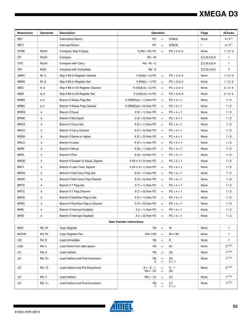
XMEGA D3
RET Subroutine Return PC ← STACK None 4 / 5(1)
RETI Interrupt Return PC ← STACK I 4 / 5(1)
CPSE Rd,Rr Compare, Skip if Equal if (Rd = Rr) PC ← PC + 2 or 3 None 1 / 2 / 3
CP Rd,Rr Compare Rd - Rr Z,C,N,V,S,H 1
CPC Rd,Rr Compare with Carry Rd - Rr - C Z,C,N,V,S,H 1
CPI Rd,K Compare with Immediate Rd - K Z,C,N,V,S,H 1
SBRC Rr, b Skip if Bit in Register Cleared if (Rr(b) = 0) PC ← PC + 2 or 3 None 1 / 2 / 3
SBRS Rr, b Skip if Bit in Register Set if (Rr(b) = 1) PC ← PC + 2 or 3 None 1 / 2 / 3
SBIC A, b Skip if Bit in I/O Register Cleared if (I/O(A,b) = 0) PC ← PC + 2 or 3 None 2 / 3 / 4
SBIS A, b Skip if Bit in I/O Register Set If (I/O(A,b) =1) PC ← PC + 2 or 3 None 2 / 3 / 4
BRBS s, k Branch if Status Flag Set if (SREG(s) = 1) then PC ← PC + k + 1 None 1 / 2
BRBC s, k Branch if Status Flag Cleared if (SREG(s) = 0) then PC ← PC + k + 1 None 1 / 2
BREQ k Branch if Equal if (Z = 1) then PC ← PC + k + 1 None 1 / 2
BRNE k Branch if Not Equal if (Z = 0) then PC ← PC + k + 1 None 1 / 2
BRCS k Branch if Carry Set if (C = 1) then PC ← PC + k + 1 None 1 / 2
BRCC k Branch if Carry Cleared if (C = 0) then PC ← PC + k + 1 None 1 / 2
BRSH k Branch if Same or Higher if (C = 0) then PC ← PC + k + 1 None 1 / 2
BRLO k Branch if Lower if (C = 1) then PC ← PC + k + 1 None 1 / 2
BRMI k Branch if Minus if (N = 1) then PC ← PC + k + 1 None 1 / 2
BRPL k Branch if Plus if (N = 0) then PC ← PC + k + 1 None 1 / 2
BRGE k Branch if Greater or Equal, Signed if (N ⊕ V= 0) then PC ← PC + k + 1 None 1 / 2
BRLT k Branch if Less Than, Signed if (N ⊕ V= 1) then PC ← PC + k + 1 None 1 / 2
BRHS k Branch if Half Carry Flag Set if (H = 1) then PC ← PC + k + 1 None 1 / 2
BRHC k Branch if Half Carry Flag Cleared if (H = 0) then PC ← PC + k + 1 None 1 / 2
BRTS k Branch if T Flag Set if (T = 1) then PC ← PC + k + 1 None 1 / 2
BRTC k Branch if T Flag Cleared if (T = 0) then PC ← PC + k + 1 None 1 / 2
BRVS k Branch if Overflow Flag is Set if (V = 1) then PC ← PC + k + 1 None 1 / 2
BRVC k Branch if Overflow Flag is Cleared if (V = 0) then PC ← PC + k + 1 None 1 / 2
BRIE k Branch if Interrupt Enabled if (I = 1) then PC ← PC + k + 1 None 1 / 2
BRID k Branch if Interrupt Disabled if (I = 0) then PC ← PC + k + 1 None 1 / 2
Data Transfer Instructions
MOV Rd, Rr Copy Register Rd ← Rr None 1
MOVW Rd, Rr Copy Register Pair Rd+1:Rd ← Rr+1:Rr None 1
LDI Rd, K Load Immediate Rd ← K None 1
LDS Rd, k Load Direct from data space Rd ← (k) None 2(1)(2)
LD Rd, X Load Indirect Rd ← (X) None 1(1)(2)
LD Rd, X+ Load Indirect and Post-Increment RdX
←←
(X)X + 1
None 1(1)(2)
LD Rd, -X Load Indirect and Pre-Decrement X ← X - 1,Rd ← (X)
←←
X - 1(X)
None 2(1)(2)
LD Rd, Y Load Indirect Rd ← (Y) ← (Y) None 1(1)(2)
LD Rd, Y+ Load Indirect and Post-Increment RdY
←←
(Y)Y + 1
None 1(1)(2)
Mnemonics Operands Description Operation Flags #Clocks
538134G–AVR–08/10
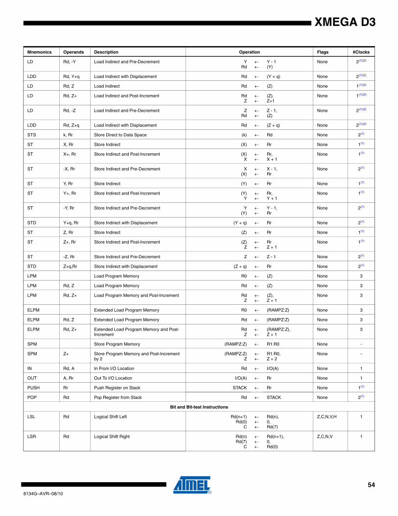
XMEGA D3
LD Rd, -Y Load Indirect and Pre-Decrement YRd
←←
Y - 1(Y)
None 2(1)(2)
LDD Rd, Y+q Load Indirect with Displacement Rd ← (Y + q) None 2(1)(2)
LD Rd, Z Load Indirect Rd ← (Z) None 1(1)(2)
LD Rd, Z+ Load Indirect and Post-Increment RdZ
←←
(Z),Z+1
None 1(1)(2)
LD Rd, -Z Load Indirect and Pre-Decrement ZRd
←←
Z - 1,(Z)
None 2(1)(2)
LDD Rd, Z+q Load Indirect with Displacement Rd ← (Z + q) None 2(1)(2)
STS k, Rr Store Direct to Data Space (k) ← Rd None 2(1)
ST X, Rr Store Indirect (X) ← Rr None 1(1)
ST X+, Rr Store Indirect and Post-Increment (X)X
←←
Rr,X + 1
None 1(1)
ST -X, Rr Store Indirect and Pre-Decrement X(X)
←←
X - 1,Rr
None 2(1)
ST Y, Rr Store Indirect (Y) ← Rr None 1(1)
ST Y+, Rr Store Indirect and Post-Increment (Y)Y
←←
Rr,Y + 1
None 1(1)
ST -Y, Rr Store Indirect and Pre-Decrement Y(Y)
←←
Y - 1,Rr
None 2(1)
STD Y+q, Rr Store Indirect with Displacement (Y + q) ← Rr None 2(1)
ST Z, Rr Store Indirect (Z) ← Rr None 1(1)
ST Z+, Rr Store Indirect and Post-Increment (Z)Z
←←
RrZ + 1
None 1(1)
ST -Z, Rr Store Indirect and Pre-Decrement Z ← Z - 1 None 2(1)
STD Z+q,Rr Store Indirect with Displacement (Z + q) ← Rr None 2(1)
LPM Load Program Memory R0 ← (Z) None 3
LPM Rd, Z Load Program Memory Rd ← (Z) None 3
LPM Rd, Z+ Load Program Memory and Post-Increment RdZ
←←
(Z),Z + 1
None 3
ELPM Extended Load Program Memory R0 ← (RAMPZ:Z) None 3
ELPM Rd, Z Extended Load Program Memory Rd ← (RAMPZ:Z) None 3
ELPM Rd, Z+ Extended Load Program Memory and Post-Increment
RdZ
←←
(RAMPZ:Z),Z + 1
None 3
SPM Store Program Memory (RAMPZ:Z) ← R1:R0 None -
SPM Z+ Store Program Memory and Post-Increment by 2
(RAMPZ:Z)Z
←←
R1:R0,Z + 2
None -
IN Rd, A In From I/O Location Rd ← I/O(A) None 1
OUT A, Rr Out To I/O Location I/O(A) ← Rr None 1
PUSH Rr Push Register on Stack STACK ← Rr None 1(1)
POP Rd Pop Register from Stack Rd ← STACK None 2(1)
Bit and Bit-test Instructions
LSL Rd Logical Shift Left Rd(n+1)Rd(0)
C
←←←
Rd(n),0,Rd(7)
Z,C,N,V,H 1
LSR Rd Logical Shift Right Rd(n)Rd(7)
C
←←←
Rd(n+1),0,Rd(0)
Z,C,N,V 1
Mnemonics Operands Description Operation Flags #Clocks
548134G–AVR–08/10
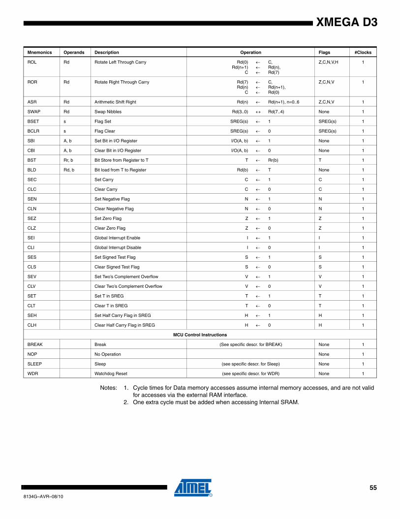
XMEGA D3
Notes: 1. Cycle times for Data memory accesses assume internal memory accesses, and are not valid for accesses via the external RAM interface.
2. One extra cycle must be added when accessing Internal SRAM.
ROL Rd Rotate Left Through Carry Rd(0)Rd(n+1)
C
←←←
C,Rd(n),Rd(7)
Z,C,N,V,H 1
ROR Rd Rotate Right Through Carry Rd(7)Rd(n)
C
←←←
C,Rd(n+1),Rd(0)
Z,C,N,V 1
ASR Rd Arithmetic Shift Right Rd(n) ← Rd(n+1), n=0..6 Z,C,N,V 1
SWAP Rd Swap Nibbles Rd(3..0) ↔ Rd(7..4) None 1
BSET s Flag Set SREG(s) ← 1 SREG(s) 1
BCLR s Flag Clear SREG(s) ← 0 SREG(s) 1
SBI A, b Set Bit in I/O Register I/O(A, b) ← 1 None 1
CBI A, b Clear Bit in I/O Register I/O(A, b) ← 0 None 1
BST Rr, b Bit Store from Register to T T ← Rr(b) T 1
BLD Rd, b Bit load from T to Register Rd(b) ← T None 1
SEC Set Carry C ← 1 C 1
CLC Clear Carry C ← 0 C 1
SEN Set Negative Flag N ← 1 N 1
CLN Clear Negative Flag N ← 0 N 1
SEZ Set Zero Flag Z ← 1 Z 1
CLZ Clear Zero Flag Z ← 0 Z 1
SEI Global Interrupt Enable I ← 1 I 1
CLI Global Interrupt Disable I ← 0 I 1
SES Set Signed Test Flag S ← 1 S 1
CLS Clear Signed Test Flag S ← 0 S 1
SEV Set Two’s Complement Overflow V ← 1 V 1
CLV Clear Two’s Complement Overflow V ← 0 V 1
SET Set T in SREG T ← 1 T 1
CLT Clear T in SREG T ← 0 T 1
SEH Set Half Carry Flag in SREG H ← 1 H 1
CLH Clear Half Carry Flag in SREG H ← 0 H 1
MCU Control Instructions
BREAK Break (See specific descr. for BREAK) None 1
NOP No Operation None 1
SLEEP Sleep (see specific descr. for Sleep) None 1
WDR Watchdog Reset (see specific descr. for WDR) None 1
Mnemonics Operands Description Operation Flags #Clocks
558134G–AVR–08/10
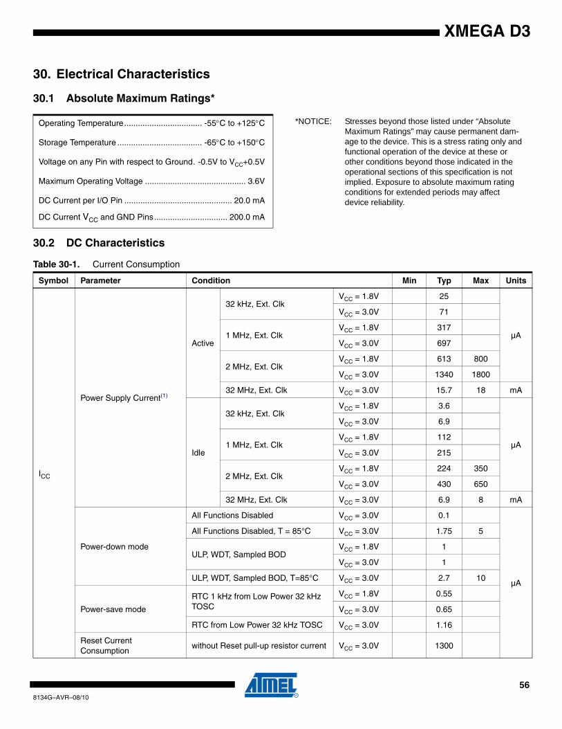
XMEGA D3
30. Electrical Characteristics
30.1 Absolute Maximum Ratings*
30.2 DC Characteristics
Operating Temperature.................................. -55°C to +125°C *NOTICE: Stresses beyond those listed under “Absolute Maximum Ratings” may cause permanent dam-age to the device. This is a stress rating only and functional operation of the device at these or other conditions beyond those indicated in the operational sections of this specification is not implied. Exposure to absolute maximum rating conditions for extended periods may affect device reliability.
Storage Temperature ..................................... -65°C to +150°C
Voltage on any Pin with respect to Ground. -0.5V to VCC+0.5V
Maximum Operating Voltage ............................................ 3.6V
DC Current per I/O Pin ............................................... 20.0 mA
DC Current VCC and GND Pins................................ 200.0 mA
Table 30-1. Current Consumption
Symbol Parameter Condition Min Typ Max Units
ICC
Power Supply Current(1)
Active
32 kHz, Ext. ClkVCC = 1.8V 25
µA
VCC = 3.0V 71
1 MHz, Ext. ClkVCC = 1.8V 317
VCC = 3.0V 697
2 MHz, Ext. ClkVCC = 1.8V 613 800
VCC = 3.0V 1340 1800
32 MHz, Ext. Clk VCC = 3.0V 15.7 18 mA
Idle
32 kHz, Ext. ClkVCC = 1.8V 3.6
µA
VCC = 3.0V 6.9
1 MHz, Ext. ClkVCC = 1.8V 112
VCC = 3.0V 215
2 MHz, Ext. ClkVCC = 1.8V 224 350
VCC = 3.0V 430 650
32 MHz, Ext. Clk VCC = 3.0V 6.9 8 mA
Power-down mode
All Functions Disabled VCC = 3.0V 0.1
µA
All Functions Disabled, T = 85°C VCC = 3.0V 1.75 5
ULP, WDT, Sampled BODVCC = 1.8V 1
VCC = 3.0V 1
ULP, WDT, Sampled BOD, T=85°C VCC = 3.0V 2.7 10
Power-save mode
RTC 1 kHz from Low Power 32 kHz TOSC
VCC = 1.8V 0.55
VCC = 3.0V 0.65
RTC from Low Power 32 kHz TOSC VCC = 3.0V 1.16
Reset Current Consumption
without Reset pull-up resistor current VCC = 3.0V 1300
568134G–AVR–08/10
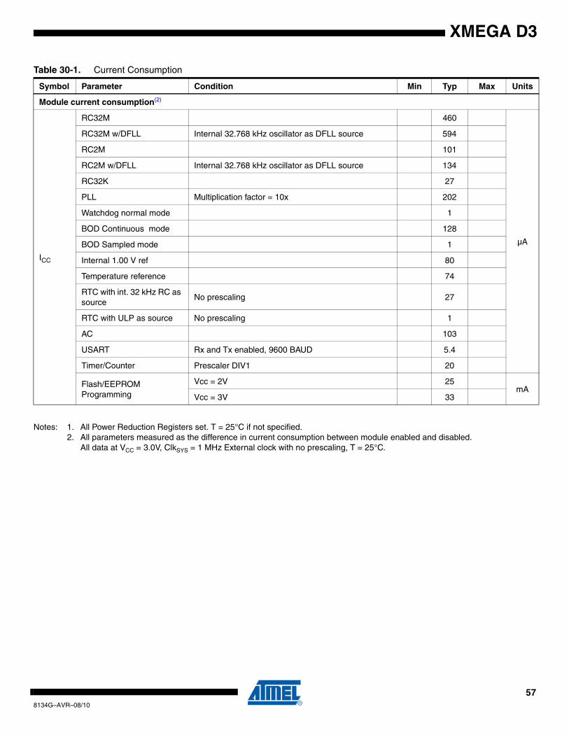
XMEGA D3
Notes: 1. All Power Reduction Registers set. T = 25°C if not specified.2. All parameters measured as the difference in current consumption between module enabled and disabled.
All data at VCC = 3.0V, ClkSYS = 1 MHz External clock with no prescaling, T = 25°C.
Module current consumption(2)
ICC
RC32M 460
µA
RC32M w/DFLL Internal 32.768 kHz oscillator as DFLL source 594
RC2M 101
RC2M w/DFLL Internal 32.768 kHz oscillator as DFLL source 134
RC32K 27
PLL Multiplication factor = 10x 202
Watchdog normal mode 1
BOD Continuous mode 128
BOD Sampled mode 1
Internal 1.00 V ref 80
Temperature reference 74
RTC with int. 32 kHz RC as source
No prescaling 27
RTC with ULP as source No prescaling 1
AC 103
USART Rx and Tx enabled, 9600 BAUD 5.4
Timer/Counter Prescaler DIV1 20
Flash/EEPROM Programming
Vcc = 2V 25mA
Vcc = 3V 33
Table 30-1. Current Consumption
Symbol Parameter Condition Min Typ Max Units
578134G–AVR–08/10
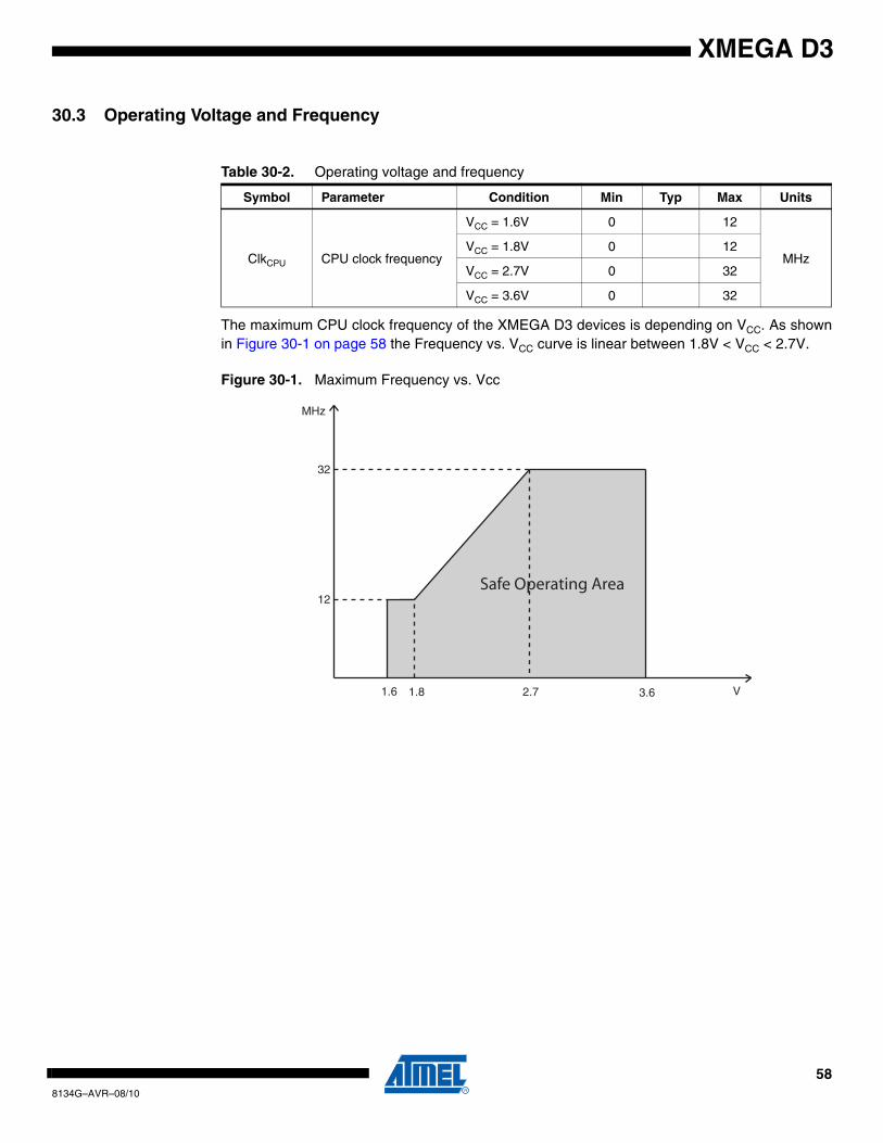
XMEGA D3
30.3 Operating Voltage and Frequency
The maximum CPU clock frequency of the XMEGA D3 devices is depending on VCC. As shownin Figure 30-1 on page 58 the Frequency vs. VCC curve is linear between 1.8V < VCC < 2.7V.
Figure 30-1. Maximum Frequency vs. Vcc
Table 30-2. Operating voltage and frequency
Symbol Parameter Condition Min Typ Max Units
ClkCPU CPU clock frequency
VCC = 1.6V 0 12
MHzVCC = 1.8V 0 12
VCC = 2.7V 0 32
VCC = 3.6V 0 32
1.8
12
32
MHz
V2.7 3.61.6
Safe Operating Area
588134G–AVR–08/10
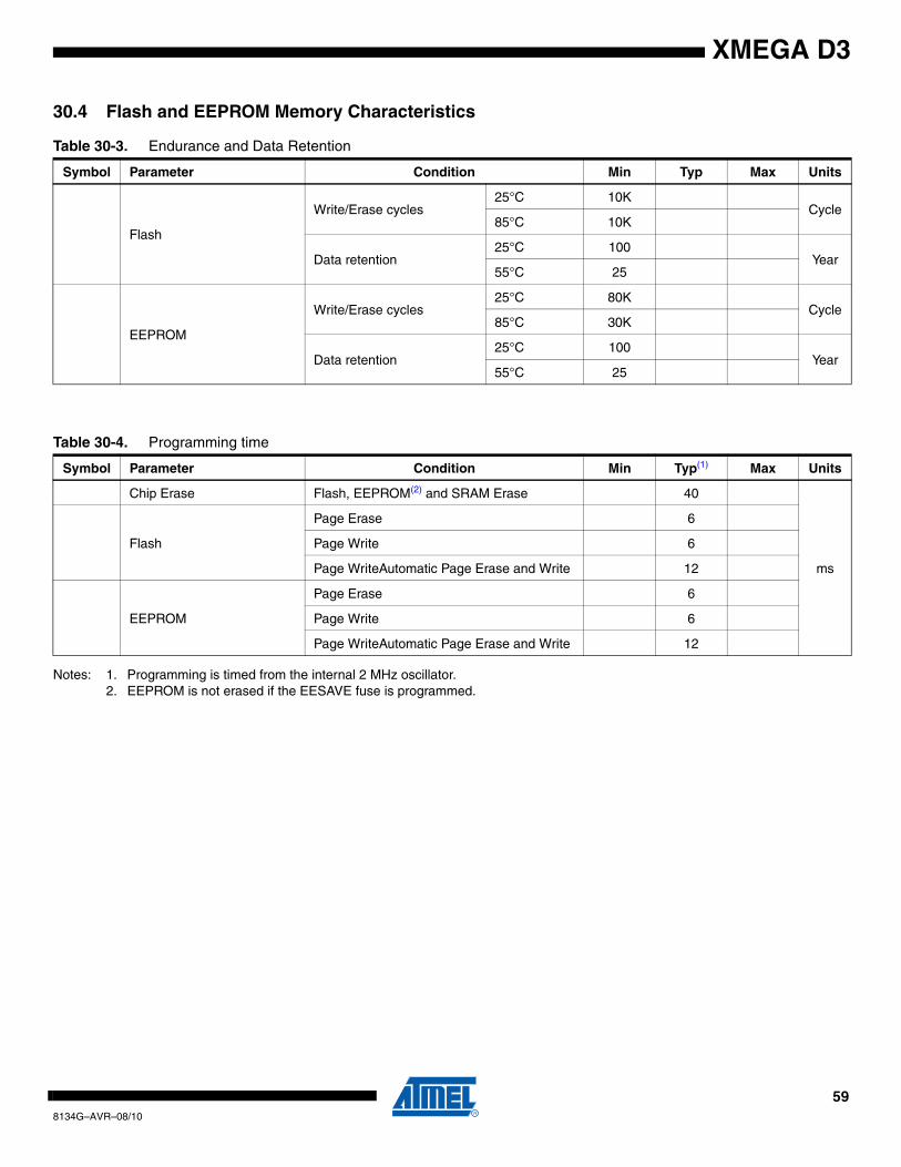
XMEGA D3
30.4 Flash and EEPROM Memory Characteristics
Notes: 1. Programming is timed from the internal 2 MHz oscillator.2. EEPROM is not erased if the EESAVE fuse is programmed.
Table 30-3. Endurance and Data Retention
Symbol Parameter Condition Min Typ Max Units
Flash
Write/Erase cycles25°C 10K
Cycle85°C 10K
Data retention25°C 100
Year55°C 25
EEPROM
Write/Erase cycles25°C 80K
Cycle85°C 30K
Data retention25°C 100
Year55°C 25
Table 30-4. Programming time
Symbol Parameter Condition Min Typ(1) Max Units
Chip Erase Flash, EEPROM(2) and SRAM Erase 40
ms
Flash
Page Erase 6
Page Write 6
Page WriteAutomatic Page Erase and Write 12
EEPROM
Page Erase 6
Page Write 6
Page WriteAutomatic Page Erase and Write 12
598134G–AVR–08/10
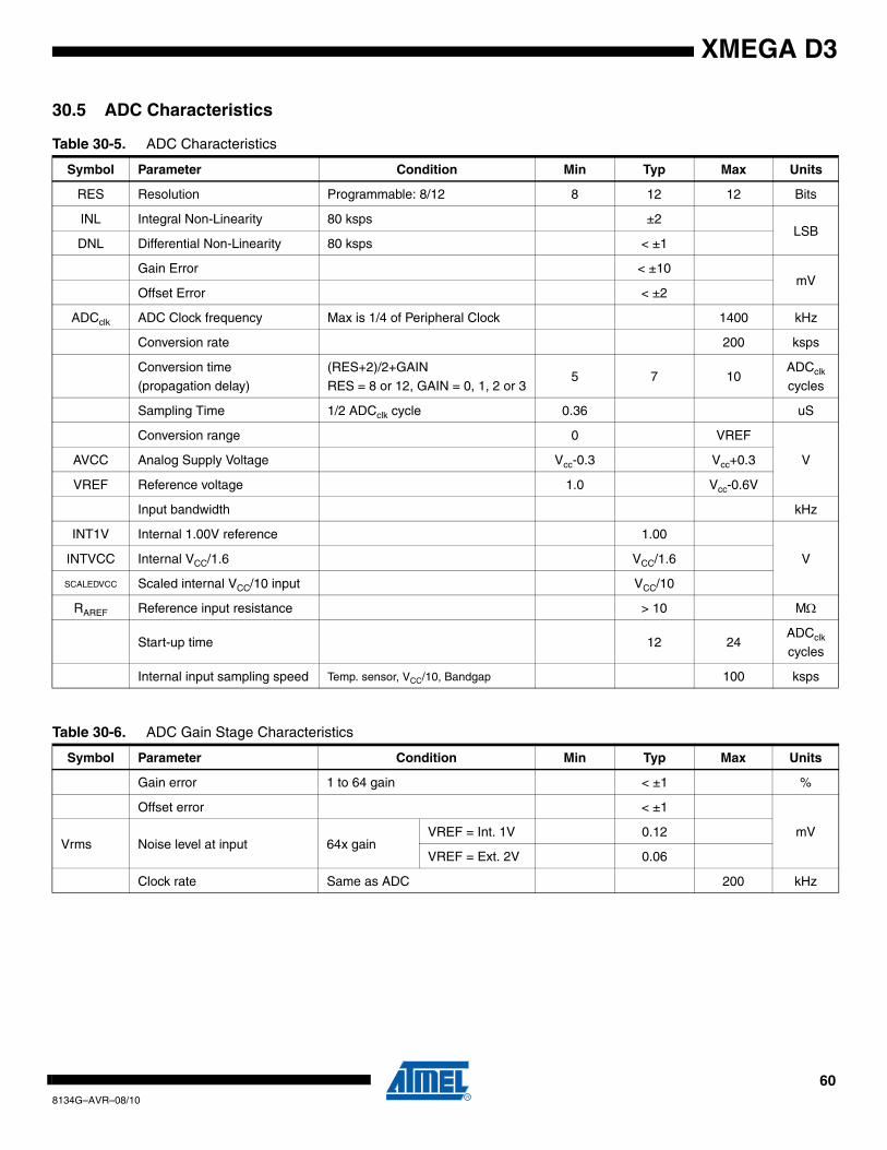
XMEGA D3
30.5 ADC Characteristics
Table 30-5. ADC Characteristics
Symbol Parameter Condition Min Typ Max Units
RES Resolution Programmable: 8/12 8 12 12 Bits
INL Integral Non-Linearity 80 ksps ±2LSB
DNL Differential Non-Linearity 80 ksps < ±1
Gain Error < ±10mV
Offset Error < ±2
ADCclk ADC Clock frequency Max is 1/4 of Peripheral Clock 1400 kHz
Conversion rate 200 ksps
Conversion time(propagation delay)
(RES+2)/2+GAIN RES = 8 or 12, GAIN = 0, 1, 2 or 3
5 7 10ADCclk
cycles
Sampling Time 1/2 ADCclk cycle 0.36 uS
Conversion range 0 VREF
VAVCC Analog Supply Voltage Vcc-0.3 Vcc+0.3
VREF Reference voltage 1.0 Vcc-0.6V
Input bandwidth kHz
INT1V Internal 1.00V reference 1.00
VINTVCC Internal VCC/1.6 VCC/1.6
SCALEDVCC Scaled internal VCC/10 input VCC/10
RAREF Reference input resistance > 10 MΩ
Start-up time 12 24ADCclk
cycles
Internal input sampling speed Temp. sensor, VCC/10, Bandgap 100 ksps
Table 30-6. ADC Gain Stage Characteristics
Symbol Parameter Condition Min Typ Max Units
Gain error 1 to 64 gain < ±1 %
Offset error < ±1
mVVrms Noise level at input 64x gain
VREF = Int. 1V 0.12
VREF = Ext. 2V 0.06
Clock rate Same as ADC 200 kHz
608134G–AVR–08/10
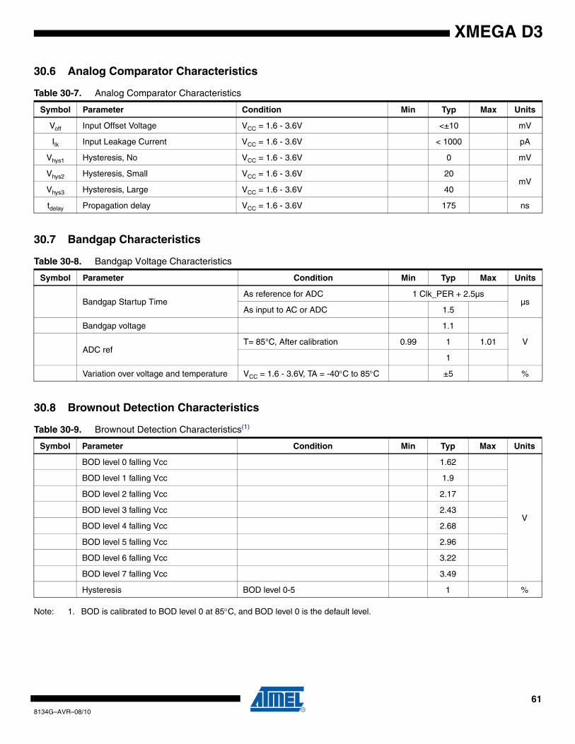
XMEGA D3
30.6 Analog Comparator Characteristics
30.7 Bandgap Characteristics
30.8 Brownout Detection Characteristics
Note: 1. BOD is calibrated to BOD level 0 at 85°C, and BOD level 0 is the default level.
Table 30-7. Analog Comparator Characteristics
Symbol Parameter Condition Min Typ Max Units
Voff Input Offset Voltage VCC = 1.6 - 3.6V <±10 mV
Ilk Input Leakage Current VCC = 1.6 - 3.6V < 1000 pA
Vhys1 Hysteresis, No VCC = 1.6 - 3.6V 0 mV
Vhys2 Hysteresis, Small VCC = 1.6 - 3.6V 20mV
Vhys3 Hysteresis, Large VCC = 1.6 - 3.6V 40
tdelay Propagation delay VCC = 1.6 - 3.6V 175 ns
Table 30-8. Bandgap Voltage Characteristics
Symbol Parameter Condition Min Typ Max Units
Bandgap Startup TimeAs reference for ADC 1 Clk_PER + 2.5µs
µsAs input to AC or ADC 1.5
Bandgap voltage 1.1
VADC ref
T= 85°C, After calibration 0.99 1 1.01
1
Variation over voltage and temperature VCC = 1.6 - 3.6V, TA = -40°C to 85°C ±5 %
Table 30-9. Brownout Detection Characteristics(1)
Symbol Parameter Condition Min Typ Max Units
BOD level 0 falling Vcc 1.62
V
BOD level 1 falling Vcc 1.9
BOD level 2 falling Vcc 2.17
BOD level 3 falling Vcc 2.43
BOD level 4 falling Vcc 2.68
BOD level 5 falling Vcc 2.96
BOD level 6 falling Vcc 3.22
BOD level 7 falling Vcc 3.49
Hysteresis BOD level 0-5 1 %
618134G–AVR–08/10
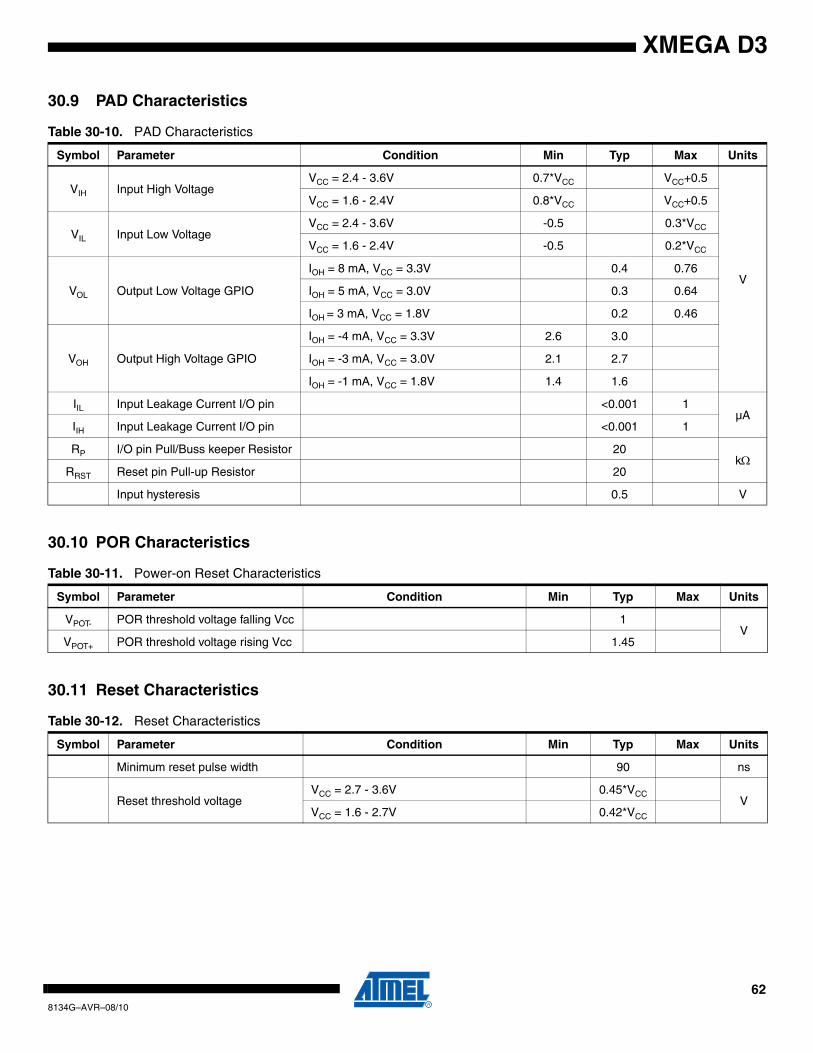
XMEGA D3
30.9 PAD Characteristics
30.10 POR Characteristics
30.11 Reset Characteristics
Table 30-10. PAD Characteristics
Symbol Parameter Condition Min Typ Max Units
VIH Input High VoltageVCC = 2.4 - 3.6V 0.7*VCC VCC+0.5
V
VCC = 1.6 - 2.4V 0.8*VCC VCC+0.5
VIL Input Low VoltageVCC = 2.4 - 3.6V -0.5 0.3*VCC
VCC = 1.6 - 2.4V -0.5 0.2*VCC
VOL Output Low Voltage GPIO
IOH = 8 mA, VCC = 3.3V 0.4 0.76
IOH = 5 mA, VCC = 3.0V 0.3 0.64
IOH = 3 mA, VCC = 1.8V 0.2 0.46
VOH Output High Voltage GPIO
IOH = -4 mA, VCC = 3.3V 2.6 3.0
IOH = -3 mA, VCC = 3.0V 2.1 2.7
IOH = -1 mA, VCC = 1.8V 1.4 1.6
IIL Input Leakage Current I/O pin <0.001 1µA
IIH Input Leakage Current I/O pin <0.001 1
RP I/O pin Pull/Buss keeper Resistor 20kΩ
RRST Reset pin Pull-up Resistor 20
Input hysteresis 0.5 V
Table 30-11. Power-on Reset Characteristics
Symbol Parameter Condition Min Typ Max Units
VPOT- POR threshold voltage falling Vcc 1V
VPOT+ POR threshold voltage rising Vcc 1.45
Table 30-12. Reset Characteristics
Symbol Parameter Condition Min Typ Max Units
Minimum reset pulse width 90 ns
Reset threshold voltageVCC = 2.7 - 3.6V 0.45*VCC
VVCC = 1.6 - 2.7V 0.42*VCC
628134G–AVR–08/10
XMEGA D3
30.12 Oscillator Characteristics
Table 30-13. Internal 32.768 kHz Oscillator Characteristics
Symbol Parameter Condition Min Typ Max Units
AccuracyT = 85°C, VCC = 3V,After production calibration
-0.5 0.5 %
Table 30-14. Internal 2 MHz Oscillator Characteristics
Symbol Parameter Condition Min Typ Max Units
AccuracyT = 85°C, VCC = 3V,After production calibration
-1.5 1.5%
DFLL Calibration step size T = 25°C, VCC = 3V 0.15
Table 30-15. Internal 32 MHz Oscillator Characteristics
Symbol Parameter Condition Min Typ Max Units
AccuracyT = 85°C, VCC = 3V,After production calibration
-1.5 1.5%
DFLL Calibration stepsize T = 25°C, VCC = 3V 0.2
Table 30-16. Internal 32 kHz, ULP Oscillator Characteristics
Symbol Parameter Condition Min Typ Max Units
Output frequency 32 kHz ULP OSC T = 85°C, VCC = 3.0V 26 kHz
Table 30-17. Maximum load capacitance (CL) and ESR recommendation for 32.768 kHz Crystal
Crystal CL [pF] Max ESR [kΩ]
6.5 60
9 35
638134G–AVR–08/10
XMEGA D3
Notes: 1. Non-prescaled System Clock source.2. Time from pin change on external interrupt pin to first available clock cycle. Additional interrupt response time is minimum 5
system clock source cycles
Table 30-18. Device wake-up time from sleep
Symbol Parameter Condition(1) Min Typ(2) Max Units
Idle Sleep, Standby and Extended Standby sleep mode
Int. 32.768 kHz RC 130
µS
Int. 2 MHz RC 2
Ext. 2 MHz Clock 2
Int. 32 MHz RC 0.17
Power-save and Power-down Sleep mode
Int. 32.768 kHz RC 320
Int. 2 MHz RC 10.3
Ext. 2 MHz Clock 4.5
Int. 32 MHz RC 5.8
648134G–AVR–08/10
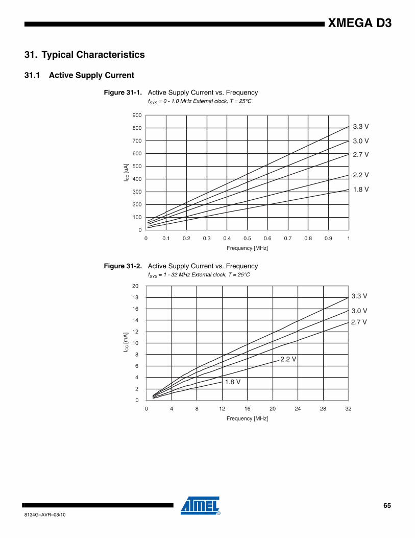
XMEGA D3
31. Typical Characteristics
31.1 Active Supply Current
Figure 31-1. Active Supply Current vs. FrequencyfSYS = 0 - 1.0 MHz External clock, T = 25°C
Figure 31-2. Active Supply Current vs. FrequencyfSYS = 1 - 32 MHz External clock, T = 25°C
3.3 V
3.0 V
2.7 V
2.2 V
1.8 V
0
100
200
300
400
500
600
700
800
900
0 0.1 0.2 0.3 0.4 0.5 0.6 0.7 0.8 0.9 1
Frequency [MHz]
I CC [u
A]
3.3 V
3.0 V
2.7 V
0
2
4
6
8
10
12
14
16
18
20
0 4 8 12 16 20 24 28 32
Frequency [MHz]
I CC [m
A]
2.2 V
1.8 V
658134G–AVR–08/10
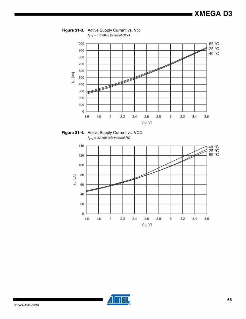
XMEGA D3
Figure 31-3. Active Supply Current vs. VccfSYS = 1.0 MHz External Clock
Figure 31-4. Active Supply Current vs. VCCfSYS = 32.768 kHz internal RC
85 °C25 °C
-40 °C
0
100
200
300
400
500
600
700
800
900
1000
1.6 1.8 2 2.2 2.4 2.6 2.8 3 3.2 3.4 3.6
VCC [V]
I CC [u
A]
85 °C25 °C
-40 °C
0
20
40
60
80
100
120
140
1.6 1.8 2 2.2 2.4 2.6 2.8 3 3.2 3.4 3.6
VCC [V]
I CC [u
A]
668134G–AVR–08/10
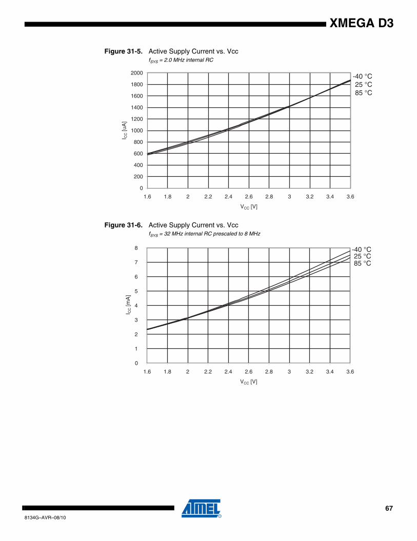
XMEGA D3
Figure 31-5. Active Supply Current vs. VccfSYS = 2.0 MHz internal RC
Figure 31-6. Active Supply Current vs. VccfSYS = 32 MHz internal RC prescaled to 8 MHz
85 °C25 °C
-40 °C
0
200
400
600
800
1000
1200
1400
1600
1800
2000
1.6 1.8 2 2.2 2.4 2.6 2.8 3 3.2 3.4 3.6
VCC [V]
I CC [u
A]
85 °C25 °C
-40 °C
0
1
2
3
4
5
6
7
8
1.6 1.8 2 2.2 2.4 2.6 2.8 3 3.2 3.4 3.6
VCC [V]
I CC [m
A]
678134G–AVR–08/10
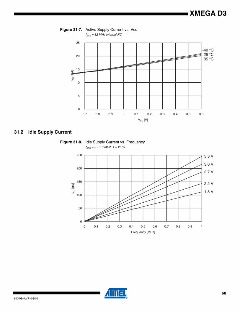
XMEGA D3
Figure 31-7. Active Supply Current vs. VccfSYS = 32 MHz internal RC
31.2 Idle Supply Current
Figure 31-8. Idle Supply Current vs. FrequencyfSYS = 0 - 1.0 MHz, T = 25°C
85 °C25 °C
-40 °C
0
5
10
15
20
25
2.7 2.8 2.9 3 3.1 3.2 3.3 3.4 3.5 3.6
VCC [V]
I CC [m
A]
3.3 V
3.0 V
2.7 V
2.2 V
1.8 V
0
50
100
150
200
250
0 0.1 0.2 0.3 0.4 0.5 0.6 0.7 0.8 0.9 1
Frequency [MHz]
I CC [u
A]
688134G–AVR–08/10
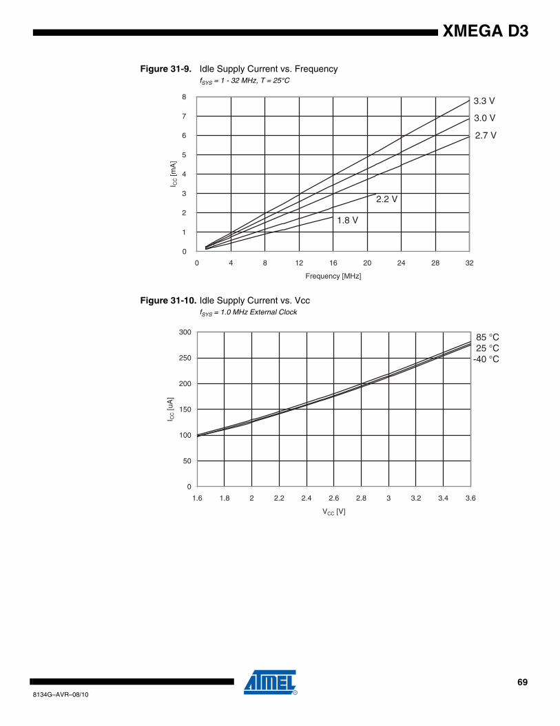
XMEGA D3
Figure 31-9. Idle Supply Current vs. FrequencyfSYS = 1 - 32 MHz, T = 25°C
Figure 31-10. Idle Supply Current vs. VccfSYS = 1.0 MHz External Clock
3.3 V
3.0 V
2.7 V
0
1
2
3
4
5
6
7
8
0 4 8 12 16 20 24 28 32
Frequency [MHz]
I CC [m
A]
1.8 V
2.2 V
85 °C25 °C
-40 °C
0
50
100
150
200
250
300
1.6 1.8 2 2.2 2.4 2.6 2.8 3 3.2 3.4 3.6
VCC [V]
I CC [u
A]
698134G–AVR–08/10
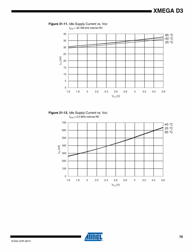
XMEGA D3
Figure 31-11. Idle Supply Current vs. VccfSYS = 32.768 kHz internal RC
Figure 31-12. Idle Supply Current vs. VccfSYS = 2.0 MHz internal RC
85 °C
25 °C-40 °C
0
5
10
15
20
25
30
35
40
1.6 1.8 2 2.2 2.4 2.6 2.8 3 3.2 3.4 3.6
VCC [V]
I CC [u
A]
85 °C25 °C
-40 °C
0
100
200
300
400
500
600
700
1.6 1.8 2 2.2 2.4 2.6 2.8 3 3.2 3.4 3.6
VCC [V]
I CC [u
A]
708134G–AVR–08/10
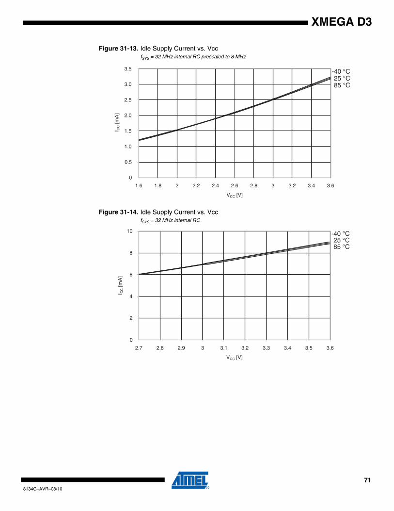
XMEGA D3
Figure 31-13. Idle Supply Current vs. VccfSYS = 32 MHz internal RC prescaled to 8 MHz
Figure 31-14. Idle Supply Current vs. VccfSYS = 32 MHz internal RC
85 °C25 °C
-40 °C
0
0.5
1.0
1.5
2.0
2.5
3.0
3.5
1.6 1.8 2 2.2 2.4 2.6 2.8 3 3.2 3.4 3.6
VCC [V]
I CC [m
A]
85 °C25 °C
-40 °C
0
2
4
6
8
10
2.7 2.8 2.9 3 3.1 3.2 3.3 3.4 3.5 3.6
VCC [V]
I CC [m
A]
718134G–AVR–08/10
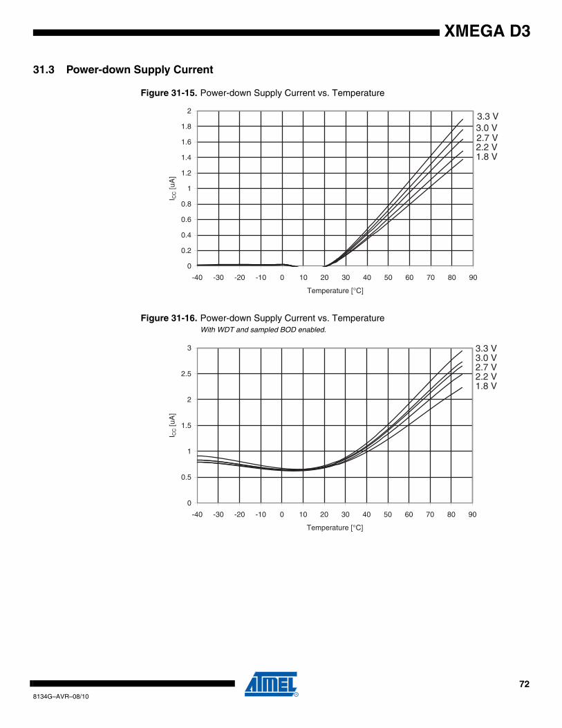
XMEGA D3
31.3 Power-down Supply Current
Figure 31-15. Power-down Supply Current vs. Temperature
Figure 31-16. Power-down Supply Current vs. TemperatureWith WDT and sampled BOD enabled.
3.3 V3.0 V2.7 V2.2 V1.8 V
0
0.2
0.4
0.6
0.8
1
1.2
1.4
1.6
1.8
2
-40 -30 -20 -10 0 10 20 30 40 50 60 70 80 90
Temperature [°C]
I CC [u
A]
3.3 V3.0 V2.7 V2.2 V1.8 V
0
0.5
1
1.5
2
2.5
3
-40 -30 -20 -10 0 10 20 30 40 50 60 70 80 90
Temperature [°C]
I CC [u
A]
728134G–AVR–08/10
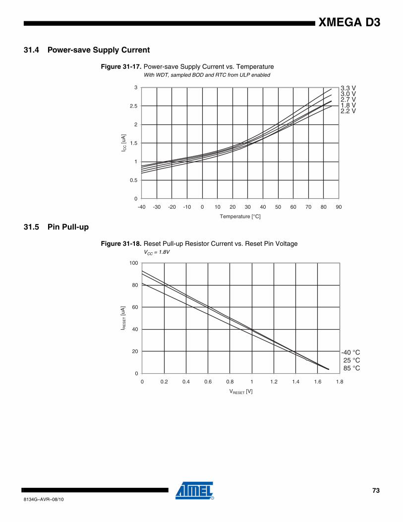
XMEGA D3
31.4 Power-save Supply Current
Figure 31-17. Power-save Supply Current vs. TemperatureWith WDT, sampled BOD and RTC from ULP enabled
31.5 Pin Pull-up
Figure 31-18. Reset Pull-up Resistor Current vs. Reset Pin VoltageVCC = 1.8V
3.3 V3.0 V2.7 V
2.2 V1.8 V
0
0.5
1
1.5
2
2.5
3
-40 -30 -20 -10 0 10 20 30 40 50 60 70 80 90
Temperature [°C]
I CC [u
A]
85 °C25 °C
-40 °C
0
20
40
60
80
100
0 0.2 0.4 0.6 0.8 1 1.2 1.4 1.6 1.8
VRESET [V]
I RE
SE
T [u
A]
738134G–AVR–08/10
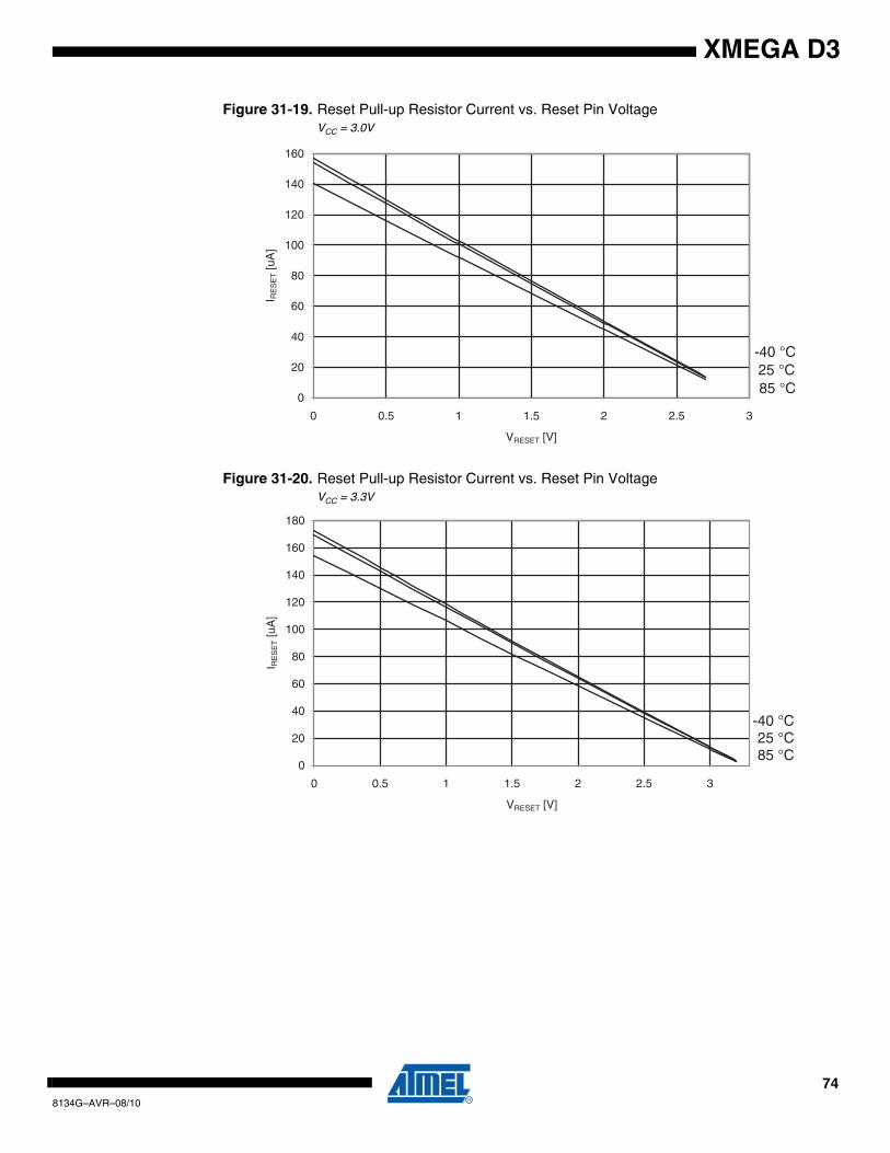
XMEGA D3
Figure 31-19. Reset Pull-up Resistor Current vs. Reset Pin VoltageVCC = 3.0V
Figure 31-20. Reset Pull-up Resistor Current vs. Reset Pin VoltageVCC = 3.3V
85 °C25 °C-40 °C
0
20
40
60
80
100
120
140
160
0 0.5 1 1.5 2 2.5 3
VRESET [V]
I RE
SE
T [u
A]
85 °C25 °C
-40 °C
0
20
40
60
80
100
120
140
160
180
0 0.5 1 1.5 2 2.5 3
VRESET [V]
I RE
SE
T [u
A]
748134G–AVR–08/10
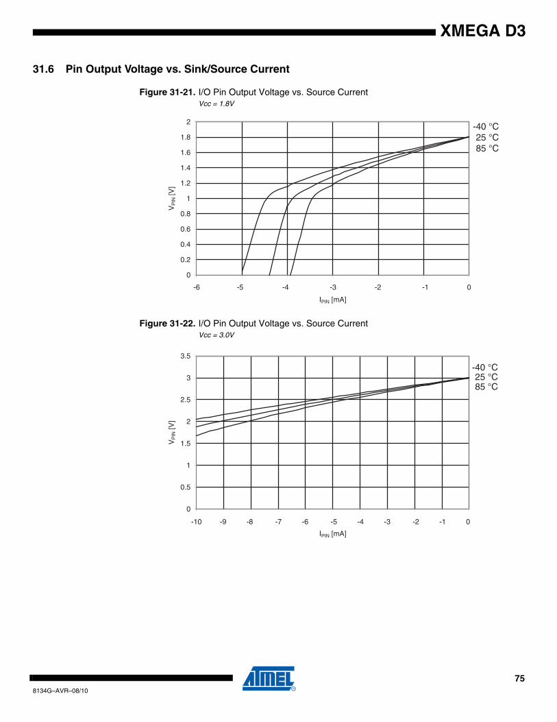
XMEGA D3
31.6 Pin Output Voltage vs. Sink/Source Current
Figure 31-21. I/O Pin Output Voltage vs. Source CurrentVcc = 1.8V
Figure 31-22. I/O Pin Output Voltage vs. Source CurrentVcc = 3.0V
85 °C25 °C
-40 °C
0
0.2
0.4
0.6
0.8
1
1.2
1.4
1.6
1.8
2
IPIN [mA]
VP
IN [V
]
-6 -5 -4 -3 -2 -1 0
85 °C25 °C
-40 °C
0
0.5
1
1.5
2
2.5
3
3.5
IPIN [mA]
VP
IN [V
]
-10 -9 -8 -7 -6 -5 -4 -3 -2 -1 0
758134G–AVR–08/10
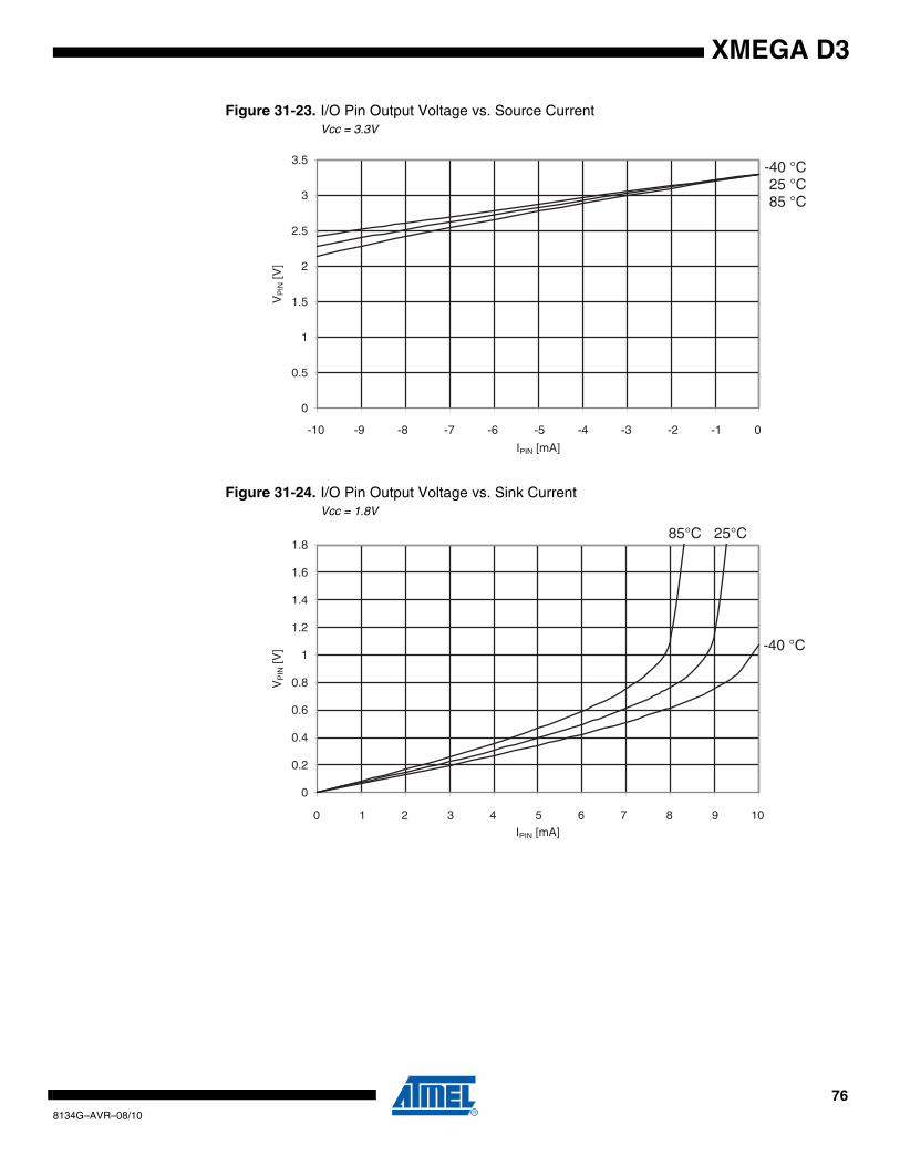
XMEGA D3
Figure 31-23. I/O Pin Output Voltage vs. Source CurrentVcc = 3.3V
Figure 31-24. I/O Pin Output Voltage vs. Sink CurrentVcc = 1.8V
85 °C25 °C
-40 °C
0
0.5
1
1.5
2
2.5
3
3.5
IPIN [mA]
VP
IN [V
]
-10 -9 -8 -7 -6 -5 -4 -3 -2 -1 0
-40 °C
0
0.2
0.4
0.6
0.8
1
1.2
1.4
1.6
1.8
IPIN [mA]
VP
IN [V
]
25°C85°C
0 1 2 3 4 5 6 7 8 9 10
768134G–AVR–08/10
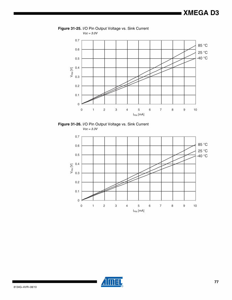
XMEGA D3
Figure 31-25. I/O Pin Output Voltage vs. Sink CurrentVcc = 3.0V
Figure 31-26. I/O Pin Output Voltage vs. Sink CurrentVcc = 3.3V
85 °C
25 °C
-40 °C
0
0.1
0.2
0.3
0.4
0.5
0.6
0.7
IPIN [mA]
VP
IN [V
]
0 1 2 3 4 5 6 7 8 9 10
85 °C
25 °C-40 °C
0
0.1
0.2
0.3
0.4
0.5
0.6
0.7
IPIN [mA]
VP
IN [V
]
0 1 2 3 4 5 6 7 8 9 10
778134G–AVR–08/10
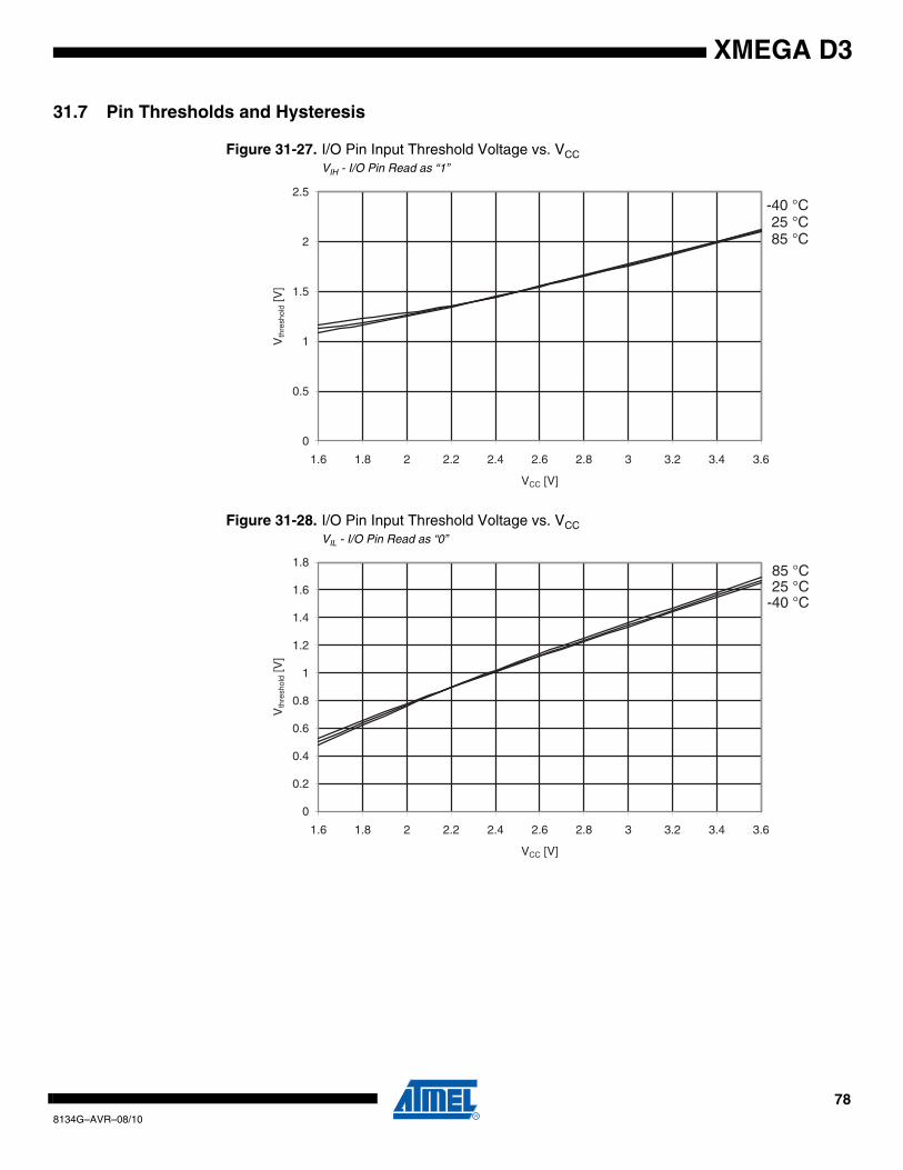
XMEGA D3
31.7 Pin Thresholds and Hysteresis
Figure 31-27. I/O Pin Input Threshold Voltage vs. VCCVIH - I/O Pin Read as “1”
Figure 31-28. I/O Pin Input Threshold Voltage vs. VCCVIL - I/O Pin Read as “0”
85 °C25 °C
-40 °C
0
0.5
1
1.5
2
2.5
1.6 1.8 2 2.2 2.4 2.6 2.8 3 3.2 3.4 3.6
VCC [V]
Vth
resh
old
[V]
85 °C25 °C
-40 °C
0
0.2
0.4
0.6
0.8
1
1.2
1.4
1.6
1.8
1.6 1.8 2 2.2 2.4 2.6 2.8 3 3.2 3.4 3.6
VCC [V]
Vth
resh
old
[V]
788134G–AVR–08/10
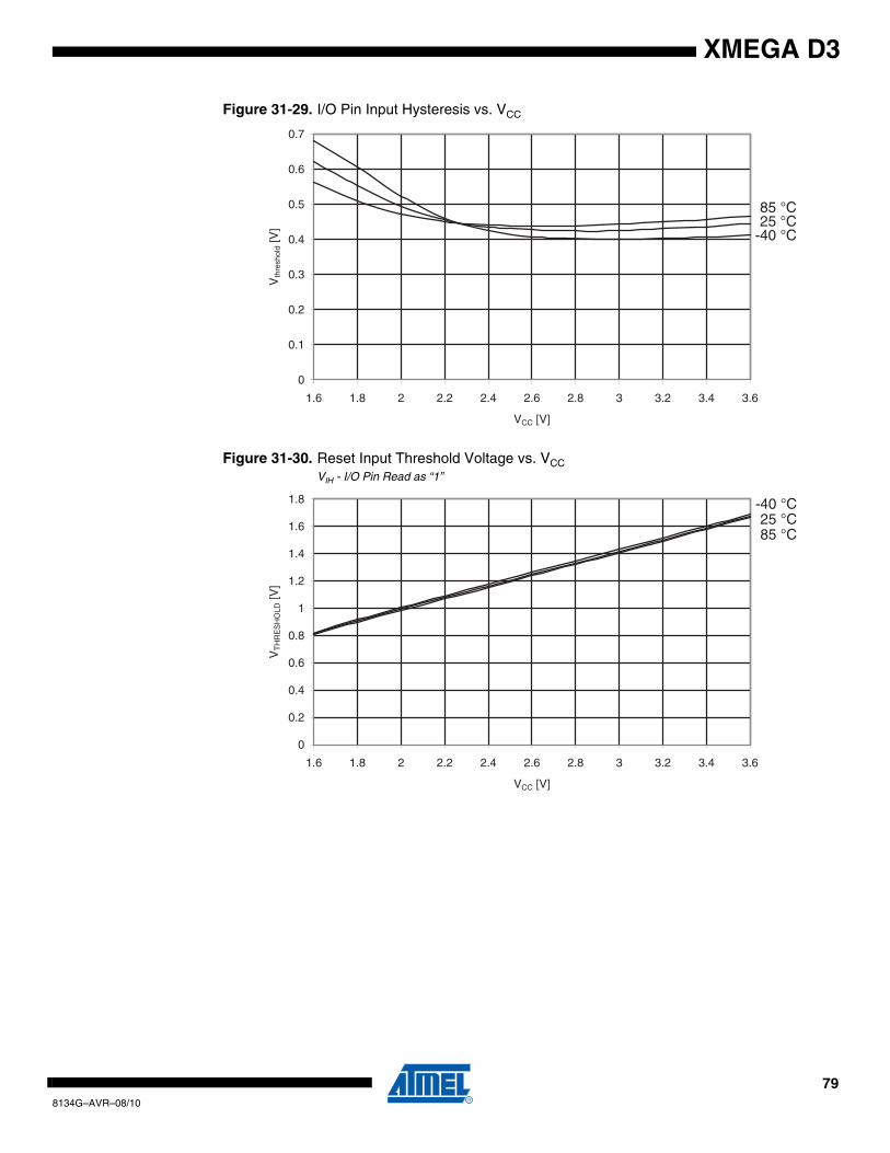
XMEGA D3
Figure 31-29. I/O Pin Input Hysteresis vs. VCC
Figure 31-30. Reset Input Threshold Voltage vs. VCC VIH - I/O Pin Read as “1”
85 °C25 °C
-40 °C
0
0.1
0.2
0.3
0.4
0.5
0.6
0.7
1.6 1.8 2 2.2 2.4 2.6 2.8 3 3.2 3.4 3.6
VCC [V]
Vth
resh
old
[V]
85 °C25 °C
-40 °C
0
0.2
0.4
0.6
0.8
1
1.2
1.4
1.6
1.8
1.6 1.8 2 2.2 2.4 2.6 2.8 3 3.2 3.4 3.6
VCC [V]
VT
HR
ES
HO
LD [V
]
798134G–AVR–08/10
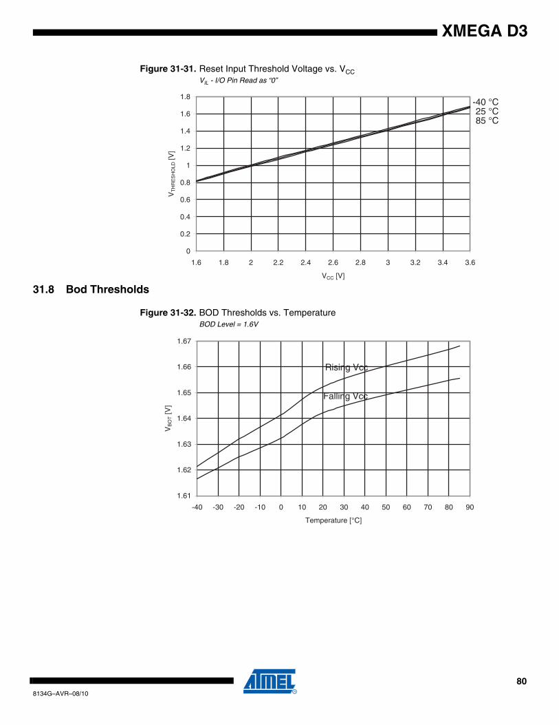
XMEGA D3
Figure 31-31. Reset Input Threshold Voltage vs. VCCVIL - I/O Pin Read as “0”
31.8 Bod Thresholds
Figure 31-32. BOD Thresholds vs. TemperatureBOD Level = 1.6V
85 °C25 °C
-40 °C
0
0.2
0.4
0.6
0.8
1
1.2
1.4
1.6
1.8
1.6 1.8 2 2.2 2.4 2.6 2.8 3 3.2 3.4 3.6
VCC [V]
VT
HR
ES
HO
LD [V
]
Rising Vcc
Falling Vcc
1.61
1.62
1.63
1.64
1.65
1.66
1.67
-40 -30 -20 -10 0 10 20 30 40 50 60 70 80 90
Temperature [°C]
VB
OT [V
]
808134G–AVR–08/10
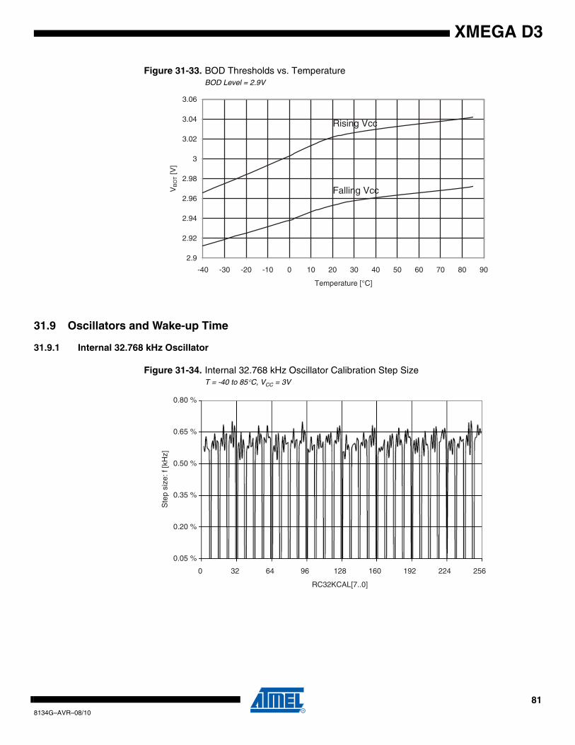
XMEGA D3
Figure 31-33. BOD Thresholds vs. TemperatureBOD Level = 2.9V
31.9 Oscillators and Wake-up Time
31.9.1 Internal 32.768 kHz Oscillator
Figure 31-34. Internal 32.768 kHz Oscillator Calibration Step SizeT = -40 to 85°C, VCC = 3V
Rising Vcc
Falling Vcc
2.9
2.92
2.94
2.96
2.98
3
3.02
3.04
3.06
-40 -30 -20 -10 0 10 20 30 40 50 60 70 80 90
Temperature [°C]
VB
OT [V
]
0 32 64 96 128 160 192 224 256
RC32KCAL[7..0]
0.05 %
0.20 %
0.35 %
0.50 %
0.65 %
0.80 %
Ste
p si
ze: f
[kH
z]
818134G–AVR–08/10
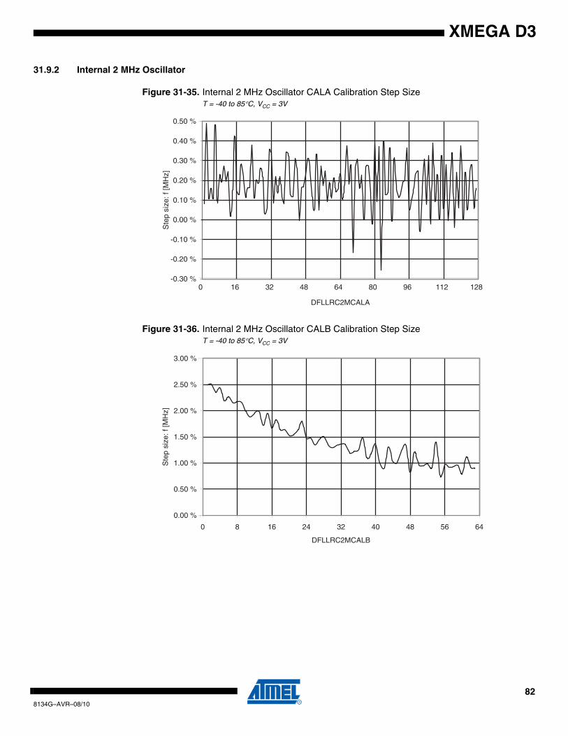
XMEGA D3
31.9.2 Internal 2 MHz Oscillator
Figure 31-35. Internal 2 MHz Oscillator CALA Calibration Step SizeT = -40 to 85°C, VCC = 3V
Figure 31-36. Internal 2 MHz Oscillator CALB Calibration Step SizeT = -40 to 85°C, VCC = 3V
-0.30 %
-0.20 %
-0.10 %
0.00 %
0.10 %
0.20 %
0.30 %
0.40 %
0.50 %
0 16 32 48 64 80 96 112 128
DFLLRC2MCALA
Ste
p si
ze: f
[MH
z]
0.00 %
0.50 %
1.00 %
1.50 %
2.00 %
2.50 %
3.00 %
0 8 16 24 32 40 48 56 64
DFLLRC2MCALB
Ste
p si
ze: f
[MH
z]
828134G–AVR–08/10
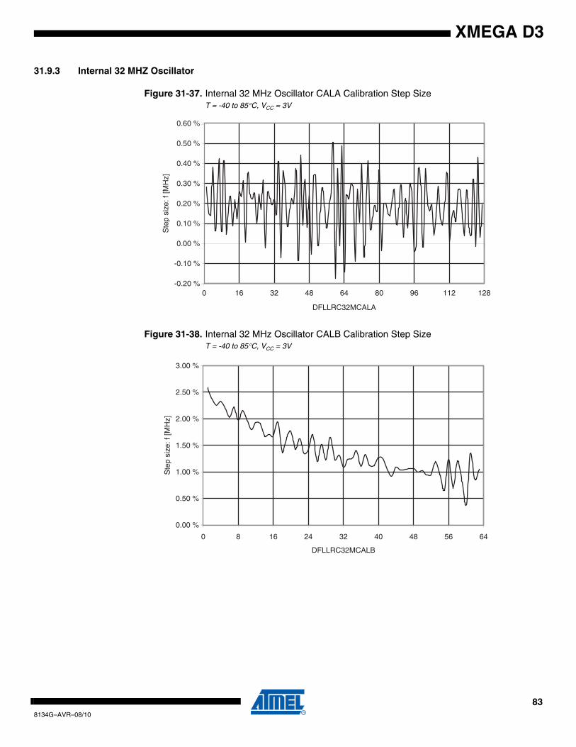
XMEGA D3
31.9.3 Internal 32 MHZ Oscillator
Figure 31-37. Internal 32 MHz Oscillator CALA Calibration Step SizeT = -40 to 85°C, VCC = 3V
Figure 31-38. Internal 32 MHz Oscillator CALB Calibration Step SizeT = -40 to 85°C, VCC = 3V
-0.20 %
-0.10 %
0.00 %
0.10 %
0.20 %
0.30 %
0.40 %
0.50 %
0.60 %
0 16 32 48 64 80 96 112 128
DFLLRC32MCALA
Ste
p si
ze: f
[MH
z]
0.00 %
0.50 %
1.00 %
1.50 %
2.00 %
2.50 %
3.00 %
0 8 16 24 32 40 48 56 64
DFLLRC32MCALB
Ste
p si
ze: f
[MH
z]
838134G–AVR–08/10
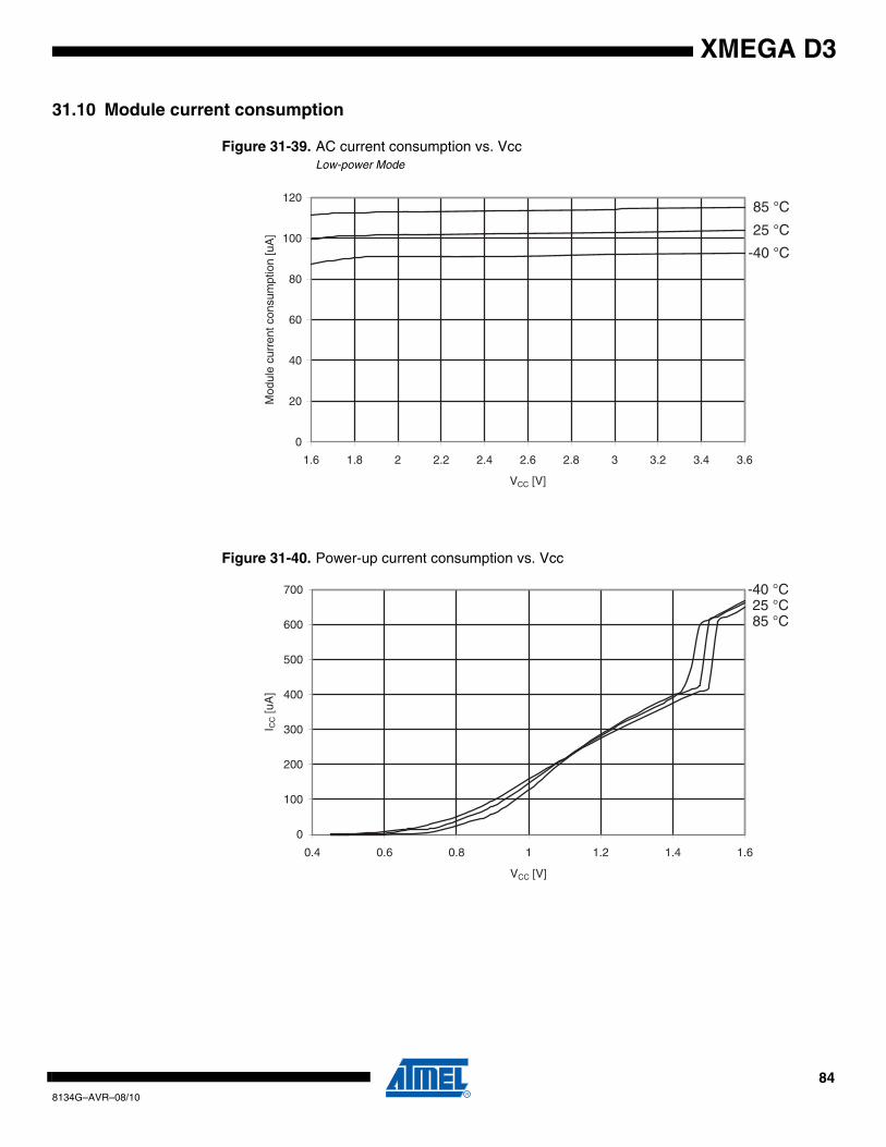
XMEGA D3
31.10 Module current consumption
Figure 31-39. AC current consumption vs. VccLow-power Mode
Figure 31-40. Power-up current consumption vs. Vcc
85 °C
25 °C
-40 °C
0
20
40
60
80
100
120
1.6 1.8 2 2.2 2.4 2.6 2.8 3 3.2 3.4 3.6
VCC [V]
Mod
ule
curr
ent c
onsu
mpt
ion
[uA
]
85 °C25 °C
-40 °C
0
100
200
300
400
500
600
700
0.4 0.6 0.8 1 1.2 1.4 1.6
VCC [V]
I CC [u
A]
848134G–AVR–08/10
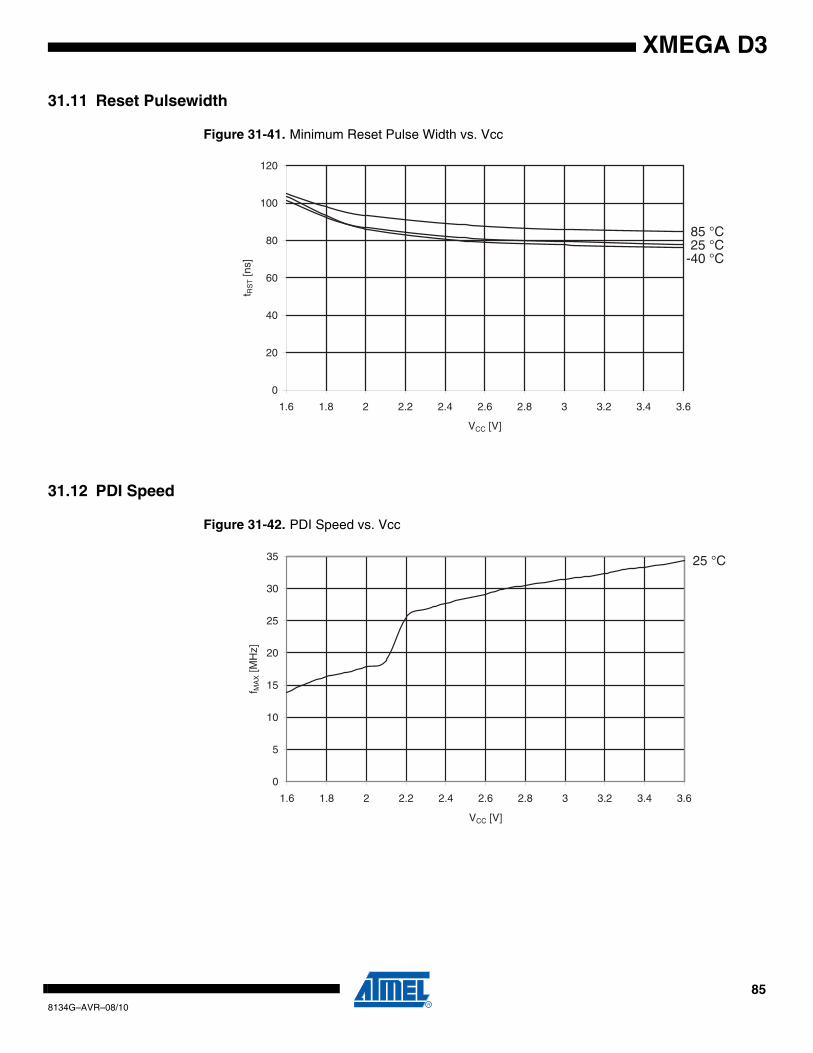
XMEGA D3
31.11 Reset Pulsewidth
Figure 31-41. Minimum Reset Pulse Width vs. Vcc
31.12 PDI Speed
Figure 31-42. PDI Speed vs. Vcc
85 °C25 °C
-40 °C
0
20
40
60
80
100
120
1.6 1.8 2 2.2 2.4 2.6 2.8 3 3.2 3.4 3.6
VCC [V]
t RS
T [n
s]
25 °C
0
5
10
15
20
25
30
35
1.6 1.8 2 2.2 2.4 2.6 2.8 3 3.2 3.4 3.6
VCC [V]
f MA
X [M
Hz]
858134G–AVR–08/10
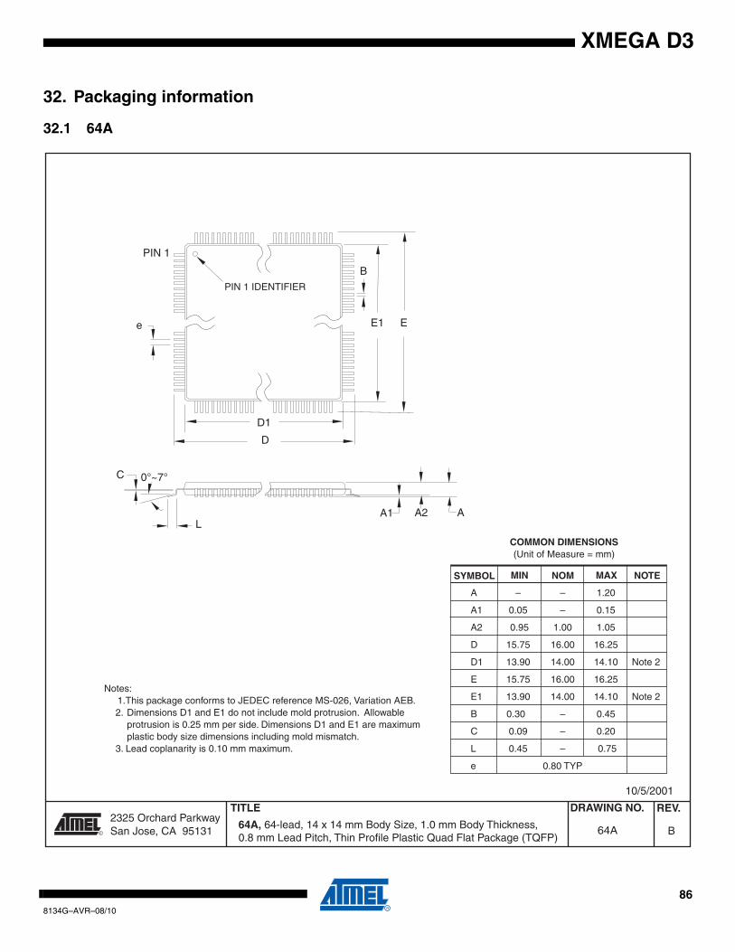
XMEGA D3
32. Packaging information
32.1 64A
2325 Orchard Parkway San Jose, CA 95131
TITLE DRAWING NO.
R
REV.
64A, 64-lead, 14 x 14 mm Body Size, 1.0 mm Body Thickness,0.8 mm Lead Pitch, Thin Profile Plastic Quad Flat Package (TQFP)
B64A
10/5/2001
PIN 1 IDENTIFIER
0°~7°
PIN 1
L
C
A1 A2 A
D1
D
e E1 E
B
COMMON DIMENSIONS(Unit of Measure = mm)
SYMBOL MIN NOM MAX NOTE
Notes: 1.This package conforms to JEDEC reference MS-026, Variation AEB. 2. Dimensions D1 and E1 do not include mold protrusion. Allowable protrusion is 0.25 mm per side. Dimensions D1 and E1 are maximum plastic body size dimensions including mold mismatch. 3. Lead coplanarity is 0.10 mm maximum.
A – – 1.20
A1 0.05 – 0.15
A2 0.95 1.00 1.05
D 15.75 16.00 16.25
D1 13.90 14.00 14.10 Note 2
E 15.75 16.00 16.25
E1 13.90 14.00 14.10 Note 2
B 0.30 – 0.45
C 0.09 – 0.20
L 0.45 – 0.75
e 0.80 TYP
868134G–AVR–08/10
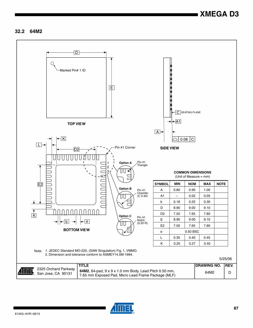
XMEGA D3
32.2 64M2
2325 Orchard Parkway San Jose, CA 95131
TITLE DRAWING NO.
R
REV. 64M2, 64-pad, 9 x 9 x 1.0 mm Body, Lead Pitch 0.50 mm, D64M2
5/25/06
COMMON DIMENSIONS(Unit of Measure = mm)
SYMBOL MIN NOM MAX NOTE
A 0.80 0.90 1.00
A1 – 0.02 0.05
b 0.18 0.25 0.30
D
D2 7.50 7.65 7.80
8.90 9.00 9.10
8.90 9.00 9.10 E
E2 7.50 7.65 7.80
e 0.50 BSC
L 0.35 0.40 0.45
TOP VIEW
SIDE VIEW
BOTTOM VIEW
D
E
Marked Pin# 1 ID
SEATING PLANE
A1
C
A
C0.08
123
K 0.20 0.27 0.40
2. Dimension and tolerance conform to ASMEY14.5M-1994.
E2
D2
b e
Pin #1 CornerL
Pin #1 Triangle
Pin #1 Chamfer(C 0.30)
Option A
Option B
Pin #1 Notch(0.20 R)
Option C
K
K
Note: 1. JEDEC Standard MO-220, (SAW Singulation) Fig. 1, VMMD.
7.65 mm Exposed Pad, Micro Lead Frame Package (MLF)
878134G–AVR–08/10
XMEGA D3
33. Errata
33.1 ATxmega256D3, ATxmega192D3, ATxmega128D3, ATxmega64D3
33.1.1 rev. B
• Bandgap voltage input for the ACs cannot be changed when used for both ACs simultaneously• Bandgap measurement with the ADC is non-functional when VCC is below 2.7V• ADC gain stage cannot be used for single conversions• ADC gain stage output range is limited to 2.4V• ADC propagation delay not correct when 8x-6x gain is used • ADC has increased INL error for some operating conditions• BOD will be enabled after any reset
• Writing EEPROM or Flash while reading any of them will not work• VCC voltage scaler for AC is non-linear• Maximum operating frequency below 1.76V is 8 MHz• TWIE is not available• Inverted I/O enable does not affect Analog Comparator Output
1. Bandgap voltage input for the ACs cannot be changed when used for both ACssimultaneouslyIf the bandgap voltage is selected as input for one Analog Comparator (AC) and thenselected/deselected as input for the another AC, the first comparator will be affected for upto 1 us and could potentially give a wrong comparison result.
Problem fix/WorkaroundIf the Bandgap is required for both ACs simultaneously, configure the input selection for bothACs before enabling any of them.
2. Bandgap measurement with the ADC is non-functional when VCC is below 2.7VThe ADC cannot be used to do bandgap measurements when VCC is below 2.7V.
Problem fix/WorkaroundIf internal voltages must be measured when VCC is below 2.7V, measure the internal 1.00Vreference instead of the bandgap.
3. ADC gain stage cannot be used for single conversionThe ADC gain stage will not output correct result for single conversions that is triggered andstarted from software or the event system.
Problem fix/Workaround
When the gain stage is used, the ADC must be set in free running mode for correct results.
4. ADC gain stage output range is limited to 2.4 VThe amplified output of the ADC gain stage will never go above 2.4 V, hence the differentialinput will only give correct output when below 2.4 V/gain. For the available gain settings, thisgives a differential input range of:
888134G–AVR–08/10
XMEGA D3
Problem fix/WorkaroundKeep the amplified voltage output from the ADC gain stage below 2.4 V in order to get a cor-rect result, or keep ADC voltage reference below 2.4 V.
5. ADC has increased INL error for some operating conditionsSome ADC configurations or operating condition will result in increased INL error.
In signed mode INL is increased to:
– 6 LSB for sample rates above 130 kSPS, and up to 8 LSB for 200 kSPS sample rate.
– 6 LSB for reference voltage below 1.1V when VCC is above 3.0V.
– 20 LSB for ambient temperature below 0 degree C and reference voltage below 1.3V.
In unsigned mode, the INL is increased up to a factor of 3 for the conditions above.
Problem fix/Workaround
None, avoid using the ADC in the above configurations in order to prevent increased INLerror.
6. ADC propagation delay not correct when 8x-64x gain is used The propagation delay will increase by only one ADC clock cycle for the 8x and 16x gain set-ting, and 32x and 64x gain settings.
Problem fix/WorkaroundNone.
7. BOD will be enabled after any resetIf any reset source goes active, the BOD will be enabled and keep the device in reset if theVCC voltage is below the programmed BOD level. During Power-On Reset, reset will not bereleased until VCC is above the programmed BOD level even if the BOD is disabled.
Problem fix/WorkaroundDo not set the BOD level higher than VCC even if the BOD is not used.
8. Writing EEPROM or Flash while reading any of them will not workThe EEPROM and Flash cannot be written while reading EEPROM or Flash, or while exe-cuting code in Active mode.
Problem fix/WorkaroundEnter IDLE sleep mode within 2.5 uS (Five 2 MHz clock cycles and 80 32 MHz clock cycles)after starting an EEPROM or flash write operation. Wake-up source must either be
– 1x gain: 2.4 V
– 2x gain: 1.2 V
– 4x gain: 0.6 V
– 8x gain: 300 mV
– 16x gain: 150 mV
– 32x gain: 75 mV
– 64x gain: 38 mV
898134G–AVR–08/10
XMEGA D3
EEPROM ready or NVM ready interrupt. Alternatively set up a Timer/Counter to give anoverflow interrupt 7 mS after the erase or write operation has started, or 13 mS after atomicerase-and-write operation has started, and then enter IDLE sleep mode.
9. VCC voltage scaler for AC is non-linearThe 6-bit VCC voltage scaler in the Analog Comparators is non-linear.
Problem fix/WorkaroundUse external voltage input for the analog comparator if accurate voltage levels are needed.
10. Maximum operating frequency below 1.76V is 8 MHzTo ensure correct operation, the maximum operating frequency below 1.76V VCC is 8 MHz.
Problem fix/WorkaroundNone, avoid running the device outside this frequency and voltage limitation.
11. TWIE is not availableThe TWI module on PORTE, TWIE is not available.
Problem fix/WorkaroundUse the identical TWI module on PORTC, TWIC instead.
12. Inverted I/O enable does not affect Analog Comparator OutputThe inverted I/O pin function does not affect the Analog Comparator output function.
Problem fix/WorkarundConfigure the analog comparator setup to give a inverted result (i.e. connect positive input tothe negative AC input and vice versa), or use and externel inverter to change polarity ofAnalog Comparator Output.
33.1.2 All rev. A
Not sampled.
908134G–AVR–08/10
XMEGA D3
34. Datasheet Revision History
Please note that the referring page numbers in this section are referred to this document. Thereferring revisions in this section are referring to the document revision.
34.1 8134G – 08/10
34.2 8134F – 02/10
34.3 8134E – 01/10
34.4 8134D – 11/09
1. Updated the Footnote 3 of ”Ordering Information” on page 2.
2. All references to CRC removed. Updated Figure 3-1 on page 5.
3. Updated ”Features” on page 26. Event Channel 0 output on port pin 7.
4. Updated ”DC Characteristics” on page 56 by adding Icc for Flash/EEPROM Programming.
5. Added AVCC in ”ADC Characteristics” on page 60.
6. Updated Start up time in ”ADC Characteristics” on page 60.
7. Updated and fixed typo in “Errata” section.
1. Added ”PDI Speed” on page 85.
1. Updated the device pin-out Figure 2-1 on page 3. PDI_CLK and PDI_DATA renamed only PDI.
2. Updated ”ADC - 12-bit Analog to Digital Converter” on page 39.
3. Updated Figure 23-1 on page 40.
4. Updated ”Alternate Pin Function Description” on page 46.
5. Updated ”Alternate Pin Functions” on page 48.
6. Updated ”Timer/Counter and AWEX functions” on page 46.
7. Added Table 30-17 on page 63.
8. Added Table 30-18 on page 64.
9. Changed Internal Oscillator Speed to ”Oscillators and Wake-up Time” on page 81.
10. Updated ”Errata” on page 88.
1. Added Table 30-3 on page 59, Endurance and Data Retention.
918134G–AVR–08/10
XMEGA D3
34.5 8134C – 10/09
34.6 8134B – 08/09
34.7 8134A – 03/09
2. Updated Table 30-10 on page 62, Input hysteresis is in V and not in mV.
3. Added ”Errata” on page 88.
4. Editing updates.
1. Updated ”Features” on page 1 with Two Two-Wire Interfaces.
2. Updated ”Block diagram and pinout” on page 3.
3. Updated ”Overview” on page 4.
4. Updated ”XMEGA D3 Block Diagram” on page 5.
5. Updated Table 13-1 on page 24.
6. Updated ”Overview” on page 35.
7. Updated Table 27-5 on page 49.
8. Updated ”Peripheral Module Address Map” on page 51.
1. Added ”Electrical Characteristics” on page 56.
2. Added ”Typical Characteristics” on page 65.
1. Initial revision.
928134G–AVR–08/10
XMEGA D3
Table of Contents
Features ..................................................................................................... 1
Typical Applications ................................................................................ 1
1 Ordering Information ............................................................................... 2
2 Pinout/ Block Diagram ............................................................................. 3
3 Overview ................................................................................................... 4
3.1Block Diagram ...........................................................................................................5
4 Resources ................................................................................................. 6
4.1Recommended reading .............................................................................................6
5 Disclaimer ................................................................................................. 6
6 AVR CPU ................................................................................................... 7
6.1Features ....................................................................................................................7
6.2Overview ...................................................................................................................7
6.3Register File ..............................................................................................................8
6.4ALU - Arithmetic Logic Unit .......................................................................................8
6.5Program Flow ............................................................................................................8
7 Memories .................................................................................................. 9
7.1Features ....................................................................................................................9
7.2Overview ...................................................................................................................9
7.3In-System Programmable Flash Program Memory ...................................................9
7.4Data Memory ...........................................................................................................11
7.5Production Signature Row .......................................................................................13
7.6User Signature Row ................................................................................................13
7.7Flash and EEPROM Page Size ...............................................................................14
8 Event System ......................................................................................... 15
8.1Features ..................................................................................................................15
8.2Overview .................................................................................................................15
9 System Clock and Clock options ......................................................... 17
9.1Features ..................................................................................................................17
9.2Overview .................................................................................................................17
9.3Clock Options ..........................................................................................................18
10 Power Management and Sleep Modes ................................................. 20
i8134G–AVR–08/10
XMEGA D3
10.1Features ................................................................................................................20
10.2Overview ...............................................................................................................20
10.3Sleep Modes .........................................................................................................20
11 System Control and Reset .................................................................... 22
11.1Features ................................................................................................................22
11.2Resetting the AVR .................................................................................................22
11.3Reset Sources .......................................................................................................22
12 WDT - Watchdog Timer ......................................................................... 23
12.1Features ................................................................................................................23
12.2Overview ...............................................................................................................23
13 PMIC - Programmable Multi-level Interrupt Controller ....................... 24
13.1Features ................................................................................................................24
13.2Overview ...............................................................................................................24
13.3Interrupt vectors ....................................................................................................24
14 I/O Ports .................................................................................................. 26
14.1Features ................................................................................................................26
14.2Overview ...............................................................................................................26
14.3I/O configuration ....................................................................................................26
14.4Input sensing .........................................................................................................29
14.5Port Interrupt .........................................................................................................29
14.6Alternate Port Functions ........................................................................................29
15 T/C - 16-bits Timer/Counter with PWM ................................................. 30
15.1Features ................................................................................................................30
15.2Overview ...............................................................................................................30
16 AWEX - Advanced Waveform Extension ............................................. 32
16.1Features ................................................................................................................32
16.2Overview ...............................................................................................................32
17 Hi-Res - High Resolution Extension ..................................................... 33
17.1Features ................................................................................................................33
17.2Overview ...............................................................................................................33
18 RTC - Real-Time Counter ...................................................................... 34
18.1Features ................................................................................................................34
18.2Overview ...............................................................................................................34
ii8134G–AVR–08/10
XMEGA D3
19 TWI - Two Wire Interface ....................................................................... 35
19.1Features ................................................................................................................35
19.2Overview ...............................................................................................................35
20 SPI - Serial Peripheral Interface ............................................................ 36
20.1Features ................................................................................................................36
20.2Overview ...............................................................................................................36
21 USART ..................................................................................................... 37
21.1Features ................................................................................................................37
21.2Overview ...............................................................................................................37
22 IRCOM - IR Communication Module .................................................... 38
22.1Features ................................................................................................................38
22.2Overview ...............................................................................................................38
23 ADC - 12-bit Analog to Digital Converter ............................................. 39
23.1Features ................................................................................................................39
23.2Overview ...............................................................................................................39
24 AC - Analog Comparator ....................................................................... 41
24.1Features ................................................................................................................41
24.2Overview ...............................................................................................................41
24.3Input Selection .......................................................................................................43
24.4Window Function ...................................................................................................43
25 OCD - On-chip Debug ............................................................................ 44
25.1Features ................................................................................................................44
25.2Overview ...............................................................................................................44
26 PDI - Program and Debug Interface ..................................................... 45
26.1Features ................................................................................................................45
26.2Overview ...............................................................................................................45
27 Pinout and Pin Functions ...................................................................... 46
27.1Alternate Pin Function Description ........................................................................46
27.2Alternate Pin Functions .........................................................................................48
28 Peripheral Module Address Map .......................................................... 51
29 Instruction Set Summary ...................................................................... 52
30 Electrical Characteristics ...................................................................... 56
iii8134G–AVR–08/10
XMEGA D3
30.1Absolute Maximum Ratings* .................................................................................56
30.2DC Characteristics ................................................................................................56
30.3Operating Voltage and Frequency ........................................................................58
30.4Flash and EEPROM Memory Characteristics .......................................................59
30.5ADC Characteristics ..............................................................................................60
30.6Analog Comparator Characteristics .......................................................................61
30.7Bandgap Characteristics .......................................................................................61
30.8Brownout Detection Characteristics ......................................................................61
30.9PAD Characteristics ..............................................................................................62
30.10POR Characteristics ............................................................................................62
30.11Reset Characteristics ..........................................................................................62
30.12Oscillator Characteristics ....................................................................................63
31 Typical Characteristics .......................................................................... 65
31.1Active Supply Current ............................................................................................65
31.2Idle Supply Current ................................................................................................68
31.3Power-down Supply Current .................................................................................72
31.4Power-save Supply Current ..................................................................................73
31.5Pin Pull-up .............................................................................................................73
31.6Pin Output Voltage vs. Sink/Source Current .........................................................75
31.7Pin Thresholds and Hysteresis ..............................................................................78
31.8Bod Thresholds .....................................................................................................80
31.9Oscillators and Wake-up Time ..............................................................................81
31.10Module current consumption ...............................................................................84
31.11Reset Pulsewidth .................................................................................................85
31.12PDI Speed ...........................................................................................................85
32 Packaging information .......................................................................... 86
32.164A ........................................................................................................................86
32.264M2 .....................................................................................................................87
33 Errata ....................................................................................................... 88
33.1ATxmega256D3, ATxmega192D3, ATxmega128D3, ATxmega64D3 ...................88
34 Datasheet Revision History .................................................................. 91
34.18134G – 08/10 .......................................................................................................91
34.28134F – 02/10 .......................................................................................................91
34.38134E – 01/10 .......................................................................................................91
34.48134D – 11/09 .......................................................................................................91
iv8134G–AVR–08/10

34.58134C – 10/09 .......................................................................................................92
34.68134B – 08/09 .......................................................................................................92
34.78134A – 03/09 .......................................................................................................92
Table of Contents....................................................................................... i
© 2010 Atmel Corporation. All rights reserved. Atmel®, Atmel logo and combinations thereof, AVR®, AVR® logo and others are registered trade-marks, XMEGATM and others are trademarks of Atmel Corporation or its subsidiaries. Other terms and product names may be trademarksof others.
Headquarters International
Atmel Corporation2325 Orchard ParkwaySan Jose, CA 95131USATel: 1(408) 441-0311Fax: 1(408) 487-2600
Atmel AsiaUnit 1-5 & 16, 19/FBEA Tower, Millennium City 5418 Kwun Tong RoadKwun Tong, KowloonHong KongTel: (852) 2245-6100Fax: (852) 2722-1369
Atmel EuropeLe Krebs8, Rue Jean-Pierre TimbaudBP 30978054 Saint-Quentin-en-Yvelines CedexFranceTel: (33) 1-30-60-70-00 Fax: (33) 1-30-60-71-11
Atmel Japan9F, Tonetsu Shinkawa Bldg.1-24-8 ShinkawaChuo-ku, Tokyo 104-0033JapanTel: (81) 3-3523-3551Fax: (81) 3-3523-7581
Product Contact
Web Sitewww.atmel.com
Technical [email protected]
Sales Contactwww.atmel.com/contacts
Literature Requestswww.atmel.com/literature
Disclaimer: The information in this document is provided in connection with Atmel products. No license, express or implied, by estoppel or otherwise, to anyintellectual property right is granted by this document or in connection with the sale of Atmel products. EXCEPT AS SET FORTH IN ATMEL’S TERMS AND CONDI-TIONS OF SALE LOCATED ON ATMEL’S WEB SITE, ATMEL ASSUMES NO LIABILITY WHATSOEVER AND DISCLAIMS ANY EXPRESS, IMPLIED OR STATUTORYWARRANTY RELATING TO ITS PRODUCTS INCLUDING, BUT NOT LIMITED TO, THE IMPLIED WARRANTY OF MERCHANTABILITY, FITNESS FOR A PARTICULARPURPOSE, OR NON-INFRINGEMENT. IN NO EVENT SHALL ATMEL BE LIABLE FOR ANY DIRECT, INDIRECT, CONSEQUENTIAL, PUNITIVE, SPECIAL OR INCIDEN-TAL DAMAGES (INCLUDING, WITHOUT LIMITATION, DAMAGES FOR LOSS OF PROFITS, BUSINESS INTERRUPTION, OR LOSS OF INFORMATION) ARISING OUT OFTHE USE OR INABILITY TO USE THIS DOCUMENT, EVEN IF ATMEL HAS BEEN ADVISED OF THE POSSIBILITY OF SUCH DAMAGES. Atmel makes norepresentations or warranties with respect to the accuracy or completeness of the contents of this document and reserves the right to make changes to specificationsand product descriptions at any time without notice. Atmel does not make any commitment to update the information contained herein. Unless specifically providedotherwise, Atmel products are not suitable for, and shall not be used in, automotive applications. Atmel’s products are not intended, authorized, or warranted for useas components in applications intended to support or sustain life.
8134G–AVR–08/10


![8/16-bit Atmel XMEGA A3BUMicrocontrollerBoard control Sensor control Utility metering White goods Optical Medical applications XMEGA A3BU [DATASHEET] 3 8362F–AVR–02/2013 2. Pinout/Block](https://img.pdfslide.us/doc/110x75/6058809cbed496644520d1ff/816-bit-atmel-xmega-a3-board-control-sensor-control-utility-metering-white-goods.jpg)


![8/16-bit Atmel AVR XMEGA Microcontrollers E5 [DATASHEET] 5 Atmel-8153H–AVR-ATxmega8E5-ATxmega16E5-ATxmega32E5_Datasheet–07/2014 4. Overview The Atmel AVR XMEGA is a family of low](https://img.pdfslide.us/doc/110x75/5ea9d1ba0c5ca912136930b1/816-bit-atmel-avr-xmega-microcontrollers-e5-datasheet-5-atmel-8153haavr-atxmega8e5-atxmega16e5-atxmega32e5datasheeta072014.jpg)


![8/16-bit Atmel AVR XMEGA Microcontrollers - caxapa.rucaxapa.ru/thumbs/406112/...16-bit-AVR-Microcontrol.pdf · XMEGA E5 [DATASHEET] 4 8153B–AVR–04/2013 4. Overview The Atmel AVR](https://img.pdfslide.us/doc/110x75/5ae0c0d27f8b9a8f298e956c/816-bit-atmel-avr-xmega-microcontrollers-e5-datasheet-4-8153bavr042013.jpg)

![Atmel AVR XMEGA C Manual - Microchip Technology · 2017. 5. 5. · XMEGA C [MANUAL] 3 Atmel-8465H-AVR-XMEGA C-12/2014 Atmel-8465H-AVR-XMEGA C-Datasheet_12/2014 2. Overview The AVR](https://img.pdfslide.us/doc/110x75/6111be10dc2737184a43a022/atmel-avr-xmega-c-manual-microchip-technology-2017-5-5-xmega-c-manual-3.jpg)