Embed Size (px)
Citation preview

STV224XH/228XH/223XHI²C BUS-CONTROLLED MULTISTANDARD
SINGLE CHIP TV PROCESSOR
■ I²C Bus Control■ PIF Circuit with PLL Demodulation
(Positive and Negative Video)■ SIF Circuit with QSS Structure, FM
Demodulation and AM Demodulation for France■ Intercarrier Capability■ Built-in Sound Bandpass■ Sound Subcarrier Output for Stereo Chassis
(FM, NICAM)■ Audio FM wide mode■ Audio Switch and Volume Control (Mono
Chassis)■ AVL (Automatic Volume Levelling)■ Integrated Chroma Filters and Luma Delay Line■ Integrated Chroma Delay Line■ Video Switch (3 CVBS In, 2 CVBS Out)■ SVHS Switch (Y Combined with CVBS3 Input)■ OSD RGB Inputs■ External RGB/YCrCb Inputs or YUV Interface■ PAL / SECAM / NTSC Chroma Demodulators■ Auto Flesh Control Capability in NTSC mode■ South America Capability (PAL-M / PAL-N /
NTSC)■ Chroma Subcarrier Output■ Black Stretch Circuit■ Peaking Circuit■ Automatic Cut-off Current Loop■ Manual Cut-off possible for low-cost
applications■ Two Horizontal Deflection PLLs■ Vertical Countdown■ Half Contrast■ APR (Automatic RGB Peak Regulation) or RGB
Peak Limitation Function ■ White Insertion ■ Copy Protection mode ■ Wide Line Blanking mode■ SAW Filter Switch Control (TQFP64 package
only)■ Very Few External Components
TQFP64 (14 x 14 x 1.4 mm)(Full Thin Plastic Quad Flat Pack)
ORDER CODE: STV223XH
SHRINK56(Plastic Package)
ORDER CODE: STV224XH/8XH
April 2004 1/86 1

STV224XH/228XH/223XH
1 GENERAL DESCRIPTION . . . . . . . . . . . . . . . . . . . . . . . . . . . . . . . . . . . . . . . . . . . . . . . . . . . . . . 61.1 INTRODUCTION . . . . . . . . . . . . . . . . . . . . . . . . . . . . . . . . . . . . . . . . . . . . . . . . . . . . . . . . . 6
1.2 PIN DESCRIPTION . . . . . . . . . . . . . . . . . . . . . . . . . . . . . . . . . . . . . . . . . . . . . . . . . . . . . . . 6
2 MAIN FEATURES . . . . . . . . . . . . . . . . . . . . . . . . . . . . . . . . . . . . . . . . . . . . . . . . . . . . . . . . . . . . 193 FUNCTIONAL DESCRIPTION . . . . . . . . . . . . . . . . . . . . . . . . . . . . . . . . . . . . . . . . . . . . . . . . . . 20
3.1 DETAILED FEATURES . . . . . . . . . . . . . . . . . . . . . . . . . . . . . . . . . . . . . . . . . . . . . . . . . . . 20
3.1.1 Power Supplies . . . . . . . . . . . . . . . . . . . . . . . . . . . . . . . . . . . . . . . . . . . . . . . . . . . . 203.1.2 Picture Intermediate Frequency (PIF) . . . . . . . . . . . . . . . . . . . . . . . . . . . . . . . . . . . 203.1.3 Sound Intermediate Frequency (SIF) and Sound Demodulators . . . . . . . . . . . . . . . 203.1.4 Audio Switch . . . . . . . . . . . . . . . . . . . . . . . . . . . . . . . . . . . . . . . . . . . . . . . . . . . . . . 203.1.5 Surface Acoustic Wave (SAW) Filter Switch Control . . . . . . . . . . . . . . . . . . . . . . . . 203.1.6 Video Switches . . . . . . . . . . . . . . . . . . . . . . . . . . . . . . . . . . . . . . . . . . . . . . . . . . . . 20
3.2 DEFLECTION PART . . . . . . . . . . . . . . . . . . . . . . . . . . . . . . . . . . . . . . . . . . . . . . . . . . . . . 21
3.2.1 Synchronization Separator . . . . . . . . . . . . . . . . . . . . . . . . . . . . . . . . . . . . . . . . . . . . 213.2.2 Two Phase-Locked Loops (PLL) . . . . . . . . . . . . . . . . . . . . . . . . . . . . . . . . . . . . . . . 213.2.3 Video Identification . . . . . . . . . . . . . . . . . . . . . . . . . . . . . . . . . . . . . . . . . . . . . . . . . . 213.2.4 Vertical Synchronization . . . . . . . . . . . . . . . . . . . . . . . . . . . . . . . . . . . . . . . . . . . . . 213.2.5 Vertical Blanking . . . . . . . . . . . . . . . . . . . . . . . . . . . . . . . . . . . . . . . . . . . . . . . . . . . 213.2.6 Vertical Oversize Blanking . . . . . . . . . . . . . . . . . . . . . . . . . . . . . . . . . . . . . . . . . . . . 213.2.7 Vertical Output . . . . . . . . . . . . . . . . . . . . . . . . . . . . . . . . . . . . . . . . . . . . . . . . . . . . . 223.2.8 Vertical Control . . . . . . . . . . . . . . . . . . . . . . . . . . . . . . . . . . . . . . . . . . . . . . . . . . . . 223.2.9 Horizontal Output . . . . . . . . . . . . . . . . . . . . . . . . . . . . . . . . . . . . . . . . . . . . . . . . . . . 223.2.10Horizontal Control . . . . . . . . . . . . . . . . . . . . . . . . . . . . . . . . . . . . . . . . . . . . . . . . . . 223.2.11Combined Line Flyback / Super-Sandcastle . . . . . . . . . . . . . . . . . . . . . . . . . . . . . . 223.2.12Line Blanking . . . . . . . . . . . . . . . . . . . . . . . . . . . . . . . . . . . . . . . . . . . . . . . . . . . . . . 223.2.13Copy Protection Mode . . . . . . . . . . . . . . . . . . . . . . . . . . . . . . . . . . . . . . . . . . . . . . . 22
3.3 FILTERS . . . . . . . . . . . . . . . . . . . . . . . . . . . . . . . . . . . . . . . . . . . . . . . . . . . . . . . . . . . . . . 22
3.3.1 Integrated Trap Filter . . . . . . . . . . . . . . . . . . . . . . . . . . . . . . . . . . . . . . . . . . . . . . . 223.3.2 Integrated Chroma Bandpass . . . . . . . . . . . . . . . . . . . . . . . . . . . . . . . . . . . . . . . . 223.3.3 Integrated Bell Filter for SECAM . . . . . . . . . . . . . . . . . . . . . . . . . . . . . . . . . . . . . . 223.3.4 Integrated Luma Delay Line . . . . . . . . . . . . . . . . . . . . . . . . . . . . . . . . . . . . . . . . . 233.3.5 Filter Tuning . . . . . . . . . . . . . . . . . . . . . . . . . . . . . . . . . . . . . . . . . . . . . . . . . . . . . . 23
3.4 VIDEO CIRCUIT . . . . . . . . . . . . . . . . . . . . . . . . . . . . . . . . . . . . . . . . . . . . . . . . . . . . . . . . 23
3.4.1 RGB Inputs . . . . . . . . . . . . . . . . . . . . . . . . . . . . . . . . . . . . . . . . . . . . . . . . . . . . . . . 233.4.2 YCrCb Mode . . . . . . . . . . . . . . . . . . . . . . . . . . . . . . . . . . . . . . . . . . . . . . . . . . . . . . 233.4.3 Half-Contrast Control . . . . . . . . . . . . . . . . . . . . . . . . . . . . . . . . . . . . . . . . . . . . . . . . 233.4.4 YUV to RGB Matrix . . . . . . . . . . . . . . . . . . . . . . . . . . . . . . . . . . . . . . . . . . . . . . . . . 233.4.5 Automatic Cut-off Current Loop . . . . . . . . . . . . . . . . . . . . . . . . . . . . . . . . . . . . . . . . 233.4.6 Warm-up Detector . . . . . . . . . . . . . . . . . . . . . . . . . . . . . . . . . . . . . . . . . . . . . . . . . . 233.4.7 Beam Current Limiter DC Voltage Input . . . . . . . . . . . . . . . . . . . . . . . . . . . . . . . . . 233.4.8 Drive (RGB gain) and DC Adjustment . . . . . . . . . . . . . . . . . . . . . . . . . . . . . . . . . . . 233.4.9 Bus-controlled Contrast & Saturation . . . . . . . . . . . . . . . . . . . . . . . . . . . . . . . . . . . . 243.4.10Bus-controlled Brightness & Sharpness . . . . . . . . . . . . . . . . . . . . . . . . . . . . . . . . . 243.4.11Bus-controlled Coring on Sharpness . . . . . . . . . . . . . . . . . . . . . . . . . . . . . . . . . . . . 243.4.12Black Stretch . . . . . . . . . . . . . . . . . . . . . . . . . . . . . . . . . . . . . . . . . . . . . . . . . . . . . . 243.4.13Bus-controlled Blue Screen . . . . . . . . . . . . . . . . . . . . . . . . . . . . . . . . . . . . . . . . . . . 243.4.14White Insertion . . . . . . . . . . . . . . . . . . . . . . . . . . . . . . . . . . . . . . . . . . . . . . . . . . . . . 243.4.15Automatic RGB Peak Regulation (APR) . . . . . . . . . . . . . . . . . . . . . . . . . . . . . . . . . 24
2/86
1

STV224XH/228XH/223XH
3.4.16RGB Peak Limitation . . . . . . . . . . . . . . . . . . . . . . . . . . . . . . . . . . . . . . . . . . . . . . . . 243.5 CHROMA CIRCUIT . . . . . . . . . . . . . . . . . . . . . . . . . . . . . . . . . . . . . . . . . . . . . . . . . . . . . . 24
3.5.1 PAL/SECAM/NTSC Decoders . . . . . . . . . . . . . . . . . . . . . . . . . . . . . . . . . . . . . . . . 243.5.2 PAL/NTSC Decoder . . . . . . . . . . . . . . . . . . . . . . . . . . . . . . . . . . . . . . . . . . . . . . . . 243.5.3 SECAM Decoder . . . . . . . . . . . . . . . . . . . . . . . . . . . . . . . . . . . . . . . . . . . . . . . . . . . 253.5.4 Chroma Standard Identification . . . . . . . . . . . . . . . . . . . . . . . . . . . . . . . . . . . . . . . . 25
4 ELECTRICAL CHARACTERISTICS . . . . . . . . . . . . . . . . . . . . . . . . . . . . . . . . . . . . . . . . . . . . . . 264.1 ABSOLUTE MAXIMUM RATINGS . . . . . . . . . . . . . . . . . . . . . . . . . . . . . . . . . . . . . . . . . . . 26
4.2 THERMAL DATA . . . . . . . . . . . . . . . . . . . . . . . . . . . . . . . . . . . . . . . . . . . . . . . . . . . . . . . . 26
4.3 SUPPLY . . . . . . . . . . . . . . . . . . . . . . . . . . . . . . . . . . . . . . . . . . . . . . . . . . . . . . . . . . . . . . . 26
4.4 IF SECTION . . . . . . . . . . . . . . . . . . . . . . . . . . . . . . . . . . . . . . . . . . . . . . . . . . . . . . . . . . . . 27
4.4.1 PIF Amplifier . . . . . . . . . . . . . . . . . . . . . . . . . . . . . . . . . . . . . . . . . . . . . . . . . . . . . . 274.4.2 PIFAGC Negative Modulation . . . . . . . . . . . . . . . . . . . . . . . . . . . . . . . . . . . . . . . . . 274.4.3 PIFAGC Positive Modulation . . . . . . . . . . . . . . . . . . . . . . . . . . . . . . . . . . . . . . . . . . 274.4.4 Tuner AGC . . . . . . . . . . . . . . . . . . . . . . . . . . . . . . . . . . . . . . . . . . . . . . . . . . . . . . . 274.4.5 Synchronous Video Demodulator . . . . . . . . . . . . . . . . . . . . . . . . . . . . . . . . . . . . 284.4.6 Demodulated Video Output (INTCVBSOUT Pin) . . . . . . . . . . . . . . . . . . . . . . . . 284.4.7 SIF Amplifier . . . . . . . . . . . . . . . . . . . . . . . . . . . . . . . . . . . . . . . . . . . . . . . . . . . . . . 294.4.8 SIF AGC (FM) . . . . . . . . . . . . . . . . . . . . . . . . . . . . . . . . . . . . . . . . . . . . . . . . . . . . . 294.4.9 SIF AGC (AM) . . . . . . . . . . . . . . . . . . . . . . . . . . . . . . . . . . . . . . . . . . . . . . . . . . . . . 294.4.10FM Demodulator . . . . . . . . . . . . . . . . . . . . . . . . . . . . . . . . . . . . . . . . . . . . . . . . . . . 294.4.11De-emphasis . . . . . . . . . . . . . . . . . . . . . . . . . . . . . . . . . . . . . . . . . . . . . . . . . . . . . . 294.4.12AM Demodulator . . . . . . . . . . . . . . . . . . . . . . . . . . . . . . . . . . . . . . . . . . . . . . . . . . 304.4.13SIF Output (AM/FM or Sound Subcarriers Output) . . . . . . . . . . . . . . . . . . . . . . . 304.4.14SAW Filter Switch Output (TQFP64 only) . . . . . . . . . . . . . . . . . . . . . . . . . . . . . . 304.4.15External Audio Input . . . . . . . . . . . . . . . . . . . . . . . . . . . . . . . . . . . . . . . . . . . . . . . 304.4.16Main Audio Output . . . . . . . . . . . . . . . . . . . . . . . . . . . . . . . . . . . . . . . . . . . . . . . . . 304.4.17AVL . . . . . . . . . . . . . . . . . . . . . . . . . . . . . . . . . . . . . . . . . . . . . . . . . . . . . . . . . . . . . 31
4.5 CVBS, Y/C, RGB INPUTS AND CVBS OUTPUTS . . . . . . . . . . . . . . . . . . . . . . . . . . . . . . 31
4.5.1 Luminance & CVBS Inputs . . . . . . . . . . . . . . . . . . . . . . . . . . . . . . . . . . . . . . . . . . 314.5.2 Combined Chrominance & SVHS Selection Input . . . . . . . . . . . . . . . . . . . . . . . 314.5.3 CVBS1 Output (Pin 29 - SDIP56) . . . . . . . . . . . . . . . . . . . . . . . . . . . . . . . . . . . . . . 314.5.4 CVBS2 Output . . . . . . . . . . . . . . . . . . . . . . . . . . . . . . . . . . . . . . . . . . . . . . . . . . . . 324.5.5 OSD RGB Inputs . . . . . . . . . . . . . . . . . . . . . . . . . . . . . . . . . . . . . . . . . . . . . . . . . . 324.5.6 FBOSD/HC Inputs . . . . . . . . . . . . . . . . . . . . . . . . . . . . . . . . . . . . . . . . . . . . . . . . . 324.5.7 External RGB/YCrCb Inputs . . . . . . . . . . . . . . . . . . . . . . . . . . . . . . . . . . . . . . . . . 334.5.8 External Fast Blanking Input . . . . . . . . . . . . . . . . . . . . . . . . . . . . . . . . . . . . . . . . 33
4.6 LUMA PART . . . . . . . . . . . . . . . . . . . . . . . . . . . . . . . . . . . . . . . . . . . . . . . . . . . . . . . . . . . . 33
4.6.1 Y Delay Line . . . . . . . . . . . . . . . . . . . . . . . . . . . . . . . . . . . . . . . . . . . . . . . . . . . . . . 334.6.2 Peaking Circuit . . . . . . . . . . . . . . . . . . . . . . . . . . . . . . . . . . . . . . . . . . . . . . . . . . . . 334.6.3 Black Stretch Control (Pin BS) . . . . . . . . . . . . . . . . . . . . . . . . . . . . . . . . . . . . . . . 344.6.4 Y Output . . . . . . . . . . . . . . . . . . . . . . . . . . . . . . . . . . . . . . . . . . . . . . . . . . . . . . . . . 34
4.7 FILTERS . . . . . . . . . . . . . . . . . . . . . . . . . . . . . . . . . . . . . . . . . . . . . . . . . . . . . . . . . . . . . . 34
4.7.1 Y Trap Filter . . . . . . . . . . . . . . . . . . . . . . . . . . . . . . . . . . . . . . . . . . . . . . . . . . . . . . 344.7.2 Chrominance Bandpass . . . . . . . . . . . . . . . . . . . . . . . . . . . . . . . . . . . . . . . . . . . . 344.7.3 Bell Filter . . . . . . . . . . . . . . . . . . . . . . . . . . . . . . . . . . . . . . . . . . . . . . . . . . . . . . . . . 35
4.8 CHROMA PART . . . . . . . . . . . . . . . . . . . . . . . . . . . . . . . . . . . . . . . . . . . . . . . . . . . . . . . . . 35
3/86

STV224XH/228XH/223XH
4.8.1 ACC . . . . . . . . . . . . . . . . . . . . . . . . . . . . . . . . . . . . . . . . . . . . . . . . . . . . . . . . . . . . . 354.8.2 ACC Overload . . . . . . . . . . . . . . . . . . . . . . . . . . . . . . . . . . . . . . . . . . . . . . . . . . . . . 354.8.3 Killer . . . . . . . . . . . . . . . . . . . . . . . . . . . . . . . . . . . . . . . . . . . . . . . . . . . . . . . . . . . . 354.8.4 Chroma PLL . . . . . . . . . . . . . . . . . . . . . . . . . . . . . . . . . . . . . . . . . . . . . . . . . . . . . . 354.8.5 PLL Loop Filter (PAL/NTSC) . . . . . . . . . . . . . . . . . . . . . . . . . . . . . . . . . . . . . . . . . . 354.8.6 Hue Control . . . . . . . . . . . . . . . . . . . . . . . . . . . . . . . . . . . . . . . . . . . . . . . . . . . . . . . 354.8.7 Automatic Flesh Control . . . . . . . . . . . . . . . . . . . . . . . . . . . . . . . . . . . . . . . . . . . . . 354.8.8 Color Demodulators . . . . . . . . . . . . . . . . . . . . . . . . . . . . . . . . . . . . . . . . . . . . . . . . . 364.8.9 Chroma Delay Line . . . . . . . . . . . . . . . . . . . . . . . . . . . . . . . . . . . . . . . . . . . . . . . . . 364.8.10Chroma Reference Output . . . . . . . . . . . . . . . . . . . . . . . . . . . . . . . . . . . . . . . . . . . . 36
4.9 SCANNING PART . . . . . . . . . . . . . . . . . . . . . . . . . . . . . . . . . . . . . . . . . . . . . . . . . . . . . . . 36
4.9.1 Synchronization Separator . . . . . . . . . . . . . . . . . . . . . . . . . . . . . . . . . . . . . . . . . . 364.9.2 Horizontal Oscillator . . . . . . . . . . . . . . . . . . . . . . . . . . . . . . . . . . . . . . . . . . . . . . . . . 364.9.3 First Loop Filter . . . . . . . . . . . . . . . . . . . . . . . . . . . . . . . . . . . . . . . . . . . . . . . . . . . . 374.9.4 Second Loop Filter . . . . . . . . . . . . . . . . . . . . . . . . . . . . . . . . . . . . . . . . . . . . . . . . . . 374.9.5 Line Flyback Input/Super-Sandcastle Output . . . . . . . . . . . . . . . . . . . . . . . . . . . . . 374.9.6 Horizontal Output . . . . . . . . . . . . . . . . . . . . . . . . . . . . . . . . . . . . . . . . . . . . . . . . . . . 374.9.7 Vertical Output . . . . . . . . . . . . . . . . . . . . . . . . . . . . . . . . . . . . . . . . . . . . . . . . . . . . 374.9.8 Vertical Amplitude Control . . . . . . . . . . . . . . . . . . . . . . . . . . . . . . . . . . . . . . . . . . . 384.9.9 Crystal Detection . . . . . . . . . . . . . . . . . . . . . . . . . . . . . . . . . . . . . . . . . . . . . . . . . . . 38
4.10 RGB CONTROL PART . . . . . . . . . . . . . . . . . . . . . . . . . . . . . . . . . . . . . . . . . . . . . . . . . . . 38
4.10.1Y Input . . . . . . . . . . . . . . . . . . . . . . . . . . . . . . . . . . . . . . . . . . . . . . . . . . . . . . . . . . . 384.10.2U & V Inputs . . . . . . . . . . . . . . . . . . . . . . . . . . . . . . . . . . . . . . . . . . . . . . . . . . . . . . 384.10.3Contrast Control . . . . . . . . . . . . . . . . . . . . . . . . . . . . . . . . . . . . . . . . . . . . . . . . . . . 384.10.4Saturation Control . . . . . . . . . . . . . . . . . . . . . . . . . . . . . . . . . . . . . . . . . . . . . . . . . . 384.10.5Brightness Control . . . . . . . . . . . . . . . . . . . . . . . . . . . . . . . . . . . . . . . . . . . . . . . . . 394.10.6RGB Matrix . . . . . . . . . . . . . . . . . . . . . . . . . . . . . . . . . . . . . . . . . . . . . . . . . . . . . . . 394.10.7Drive Adjustment (White Point Adjustment) . . . . . . . . . . . . . . . . . . . . . . . . . . . . . . 394.10.8Cut-Off Adjustment (Black Point Adjustment) . . . . . . . . . . . . . . . . . . . . . . . . . . . . . 394.10.9Cathode Current Input . . . . . . . . . . . . . . . . . . . . . . . . . . . . . . . . . . . . . . . . . . . . . . 394.10.10Beam Current Limiter Input . . . . . . . . . . . . . . . . . . . . . . . . . . . . . . . . . . . . . . . . . . 394.10.11Automatic RGB Peak Regulation (APR) / RGB Peak Limitation . . . . . . . . . . . . . . 404.10.12RGB Outputs . . . . . . . . . . . . . . . . . . . . . . . . . . . . . . . . . . . . . . . . . . . . . . . . . . . . . 41
4.11 I²C BUS CHARACTERISTICS . . . . . . . . . . . . . . . . . . . . . . . . . . . . . . . . . . . . . . . . . . . . . . 43
4.11.1SCL . . . . . . . . . . . . . . . . . . . . . . . . . . . . . . . . . . . . . . . . . . . . . . . . . . . . . . . . . . . . . 434.11.2SDA . . . . . . . . . . . . . . . . . . . . . . . . . . . . . . . . . . . . . . . . . . . . . . . . . . . . . . . . . . . . . 434.11.3I²C Timing . . . . . . . . . . . . . . . . . . . . . . . . . . . . . . . . . . . . . . . . . . . . . . . . . . . . . . . . 43
5 I²C BUS SPECIFICATIONS . . . . . . . . . . . . . . . . . . . . . . . . . . . . . . . . . . . . . . . . . . . . . . . . . . . . 446 I²C BUS SELECTION . . . . . . . . . . . . . . . . . . . . . . . . . . . . . . . . . . . . . . . . . . . . . . . . . . . . . . . . . 45
6.1 SUMMARY INPUT SIGNALS (WRITE MODE) . . . . . . . . . . . . . . . . . . . . . . . . . . . . . . . . . 45
6.2 SUMMARY OUTPUT SIGNALS (READ MODE) . . . . . . . . . . . . . . . . . . . . . . . . . . . . . . . 46
6.3 INPUT SIGNALS (WRITE MODE) . . . . . . . . . . . . . . . . . . . . . . . . . . . . . . . . . . . . . . . . . . . 47
6.3.1 PIFVCO Free Running . . . . . . . . . . . . . . . . . . . . . . . . . . . . . . . . . . . . . . . . . . . . . . 476.3.2 PIF Free Running Coarse . . . . . . . . . . . . . . . . . . . . . . . . . . . . . . . . . . . . . . . . . . . . 476.3.3 PIF Features . . . . . . . . . . . . . . . . . . . . . . . . . . . . . . . . . . . . . . . . . . . . . . . . . . . . . . 476.3.4 Tuner Delay . . . . . . . . . . . . . . . . . . . . . . . . . . . . . . . . . . . . . . . . . . . . . . . . . . . . . . . 486.3.5 SIF Features and Audio Switches . . . . . . . . . . . . . . . . . . . . . . . . . . . . . . . . . . . . . . 486.3.6 Video Controls . . . . . . . . . . . . . . . . . . . . . . . . . . . . . . . . . . . . . . . . . . . . . . . . . . . . . 49
4/86

STV224XH/228XH/223XH
6.3.7 Chroma Controls . . . . . . . . . . . . . . . . . . . . . . . . . . . . . . . . . . . . . . . . . . . . . . . . . . . 516.3.8 Scanning Controls . . . . . . . . . . . . . . . . . . . . . . . . . . . . . . . . . . . . . . . . . . . . . . . . . . 526.3.9 Miscellaneous . . . . . . . . . . . . . . . . . . . . . . . . . . . . . . . . . . . . . . . . . . . . . . . . . . . . 53
6.4 OUTPUT SIGNALS (READ MODE) . . . . . . . . . . . . . . . . . . . . . . . . . . . . . . . . . . . . . . . . . 54
6.5 POWER-ON RESET - INITIAL BUS REGISTER CONDITIONS . . . . . . . . . . . . . . . . . . . . 56
7 I²C BUS SPECIFICATION COMPATIBILITY . . . . . . . . . . . . . . . . . . . . . . . . . . . . . . . . . . . . . . . 578 INPUT/OUTPUT SCHEMATIC DIAGRAMS . . . . . . . . . . . . . . . . . . . . . . . . . . . . . . . . . . . . . . . . 589 APPLICATION DIAGRAMS . . . . . . . . . . . . . . . . . . . . . . . . . . . . . . . . . . . . . . . . . . . . . . . . . . . . 7910 THERMAL CONSIDERATIONS FOR TQFP64 PACKAGE . . . . . . . . . . . . . . . . . . . . . . . . . . . 8311 SUMMARY OF CHANGES . . . . . . . . . . . . . . . . . . . . . . . . . . . . . . . . . . . . . . . . . . . . . . . . . . . . 8412 GENERAL PACKAGE INFORMATION . . . . . . . . . . . . . . . . . . . . . . . . . . . . . . . . . . . . . . . . . . 85
12.1 PACKAGE MECHANICAL DATA . . . . . . . . . . . . . . . . . . . . . . . . . . . . . . . . . . . . . . . . . . . . 85
5/86

STV224XH/228XH/223XH - GENERAL DESCRIPTION
1 GENERAL DESCRIPTION
1.1 INTRODUCTION
The STV224XH/228XH/223XH are fully bus-controlled ICs for TV that include PIF, SIF, Luma, Chromaand Deflection processing functions. Used with a vertical frame booster (TDA8174A for a 90° chassis,STV9306 for a 110° chassis), they allow multistandard (BGDKIMNLL’, PAL/SECAM/NTSC) sets to be de-signed with very few external components and no manual adjustments.
1.2 PIN DESCRIPTION
Table 1. Pin Configuration
Package
Application
PAL/NTSCIntercarrier
PAL/NTSCQSS/Intercarrier
PAL/SECAM/NTSCQSS/Intercarrier
AM
PAL/SECAM/NTSCQSS/Intercarrier
SHRINK56 STV2246H/86H STV2247H STV2248H STV2249H
TQFP64 STV2236H STV2237H STV2238H STV2239H
Function 2246H/36H 2286H 2247H/37H 2248H/38H 2249H/39HPAL/SECAM/NTSC X X
PAL/NTSC X X X
QSS/Intercarrier X X XIntercarrier Only X X
AM X
Audio FM Wide mode with QSS Application X X X1 EXT RGB Input (OSD) X
OSD RGB Inputs & RGBEXT/YCrCb Inputs X X X X
PINSymbol DescriptionSTV224XH/228XH STV223XH
SDIP56 TQFP641 8 SIFIN1 SIF Input (Please refer to Note 1)2 9 SIFIN2 SIF Input (Please refer to Note 1)
3 10 AGCSIFCAP AGC SIF Capacitor (Please refer to Note 1)
4 11 VREFIF Voltage Reference Filtering5 12 AGCPIFCAP AGC PIF Capacitor
6 13 PIFIN1 PIF Input
7 14 PIFIN2 PIF Input- 15 SAW Filter Switch Control
8 16 TUNERAGCOUT AGC Tuner Output
9 17 IFPLL IF PLL Filter10 18 GNDIF IF Ground
11 19 AM/FMOUT/SC AM/FM Mono Sound or Stereo Carriers Output
12 20 VCCIF 5 V IF Supply13 21 INTCVBSOUT Internal CVBS Output
14 22 EXTAUDIOIN External Audio Input
15 23 PIFLC1 LC Input16 24 PIFLC2 LC Input
17 25 VCC2 Video/Luma Supply Voltage (8 V)
18 26 CVBSIN1 Internal Video Input
6/86
2

STV224XH/228XH/223XH - GENERAL DESCRIPTION
19 27 GND2 Video/Luma Ground
20 28 CVBSIN2 External Video Input
21 29 BS Black Stretch Capacitor22 34 Y/CVBSIN3 Y(SVHS) or CVBS3 External Input
23 35 CHR Chroma (SVHS) Input
24 36 APR Automatic RGB Peak Regulation
25 37 BEXT/CbExternal Blue Input or external Cb Input(Please refer to Note 2)
26 38 GEXT/YExternal Green Input or external Y Input(Please refer to Note 2)
27 39 REXT/CrExternal Red Input or external Cr Input(Please refer to Note 2)
28 40 FBEXTExternal Fast Blanking Input (Please refer to Note 3)
29 41 NTBC/CVBSOUT1Not To Be Connected or CVBS Output 1(Please refer to Note 4)
30 43 BOUT Blue Output
31 44 GOUT Green Output
32 45 ROUT Red Output33 46 ICATH Cathode Current Measurement Input
34 47 BOSD OSD Blue Input
35 48 GOSD OSD Green Input36 49 ROSD OSD Red Input
37 50 FBOSD/HC OSD Fast Blanking Input / Half Contrast
38 52 XTAL3/BTUN 3.5X MHz Crystal or Bell Filter Tuning Capacitor39 53 XTAL2 3.5X MHz Crystal
40 54 XTAL1 4.43/3.5X MHz Crystal
41 55 CLPF Chroma PLL Filter
42 56 X1/VAMP/CHROUTXTAL1 Control Pin, Vertical Amplitude DAC Output and Chroma Reference Signal Output
43 57 GND1 Chroma/Scanning Ground
44 58 CVBSOUT2 Second Video Switch Output
45 59 VCC1 Chroma/Scanning Power Supply (8 V)
46 61 BCL/SAFBeam Current Limiter Control Voltage and Safe-ty Input (XRAY)
47 62 VERT Vertical Output Pulse
48 63 HOUT Horizontal Output Pulse
49 64 LFB/SSCLine Flyback Input and Super-Sandcastle Out-put
50 1 SLPF Scanning PLL Filter
51 2 SCL I²C Bus Clock Input
52 3 SDA I²C Bus Data Input53 4 VCCD Digital Supply Voltage (5 V)
54 5 GNDD Digital Ground
55 6 AUDIOOUT Main Audio Output56 7 FMCAP FM Demodulation Capacitor
- 30 NC Connection to GND recommended
PINSymbol DescriptionSTV224XH/228XH STV223XH
SDIP56 TQFP64
7/86
2

STV224XH/228XH/223XH - GENERAL DESCRIPTION
Note 1: Input/Output not available in STV2246H/86H versions. This pin must not be connected.Note 2: When REXT, GEXT and BEXT pins are not used, they must not be connected. Register 0Ah must be set (d7 and
d6 = 01). (RGB external inputs disabled.)Note 3: FBEXT to be connected to ground when not used.Note 4: CVBS output 1 on pin 29 (SDIP56), if register 1Dh = 07h.
Figure 1. STV224XH/228XH Pinout (SDIP56)
Note: Underlined pin functions are optional.
- 31 NC Connection to GND recommended
- 32 NC Connection to GND recommended
- 33 NC Connection to GND recommended- 42 NC Connection to GND recommended
- 51 NC Connection to GND recommended
- 60 NC Connection to GND recommended
PINSymbol DescriptionSTV224XH/228XH STV223XH
SDIP56 TQFP64
SIFIN1
SIFIN2
AGCSIFCAP
VREFIF
AGCPIFCAP
PIFIN1
PIFIN2
TUNERAGCOUT
IFPLL
GNDIF
AM/FMOUT/SC
VCCIF
INTCVBSOUT
EXTAUDIOIN
PIFLC1
PIFLC2
VCC2
CVBSIN1
GND2
CVBSIN2
BS
Y/CVBSIN3
CHR
APR
BEXT/Cb
GEXT/Y
REXT/Cr
FBEXT
FMCAP
AUDIOOUT
GNDD
VCCD
SDA
SCL
SLPF
LFB/SSC
HOUT
VERT
BCL/SAF
VCC1
CVBSOUT2
GND1
X1/VAMP/CHROUT
CLPF
XTAL1
XTAL2
XTAL3/BTUN
ROSD
GOSD
BOSD
ICATH
ROUT
GOUT
BOUT
NTBC/CVBSOUT1
FBOSD/HC
1
2
3
4
5
6
7
8
9
10
11
12
13
14
15
16
17
18
19
20
21
22
23
24
25
26
27
28
56
55
54
53
52
51
50
49
48
47
46
45
44
43
42
41
40
39
38
37
36
35
34
33
32
31
30
29
8/86

STV224XH/228XH/223XH - GENERAL DESCRIPTION
Figure 2. STV223Xh Pinout (TQFP64)
TUNERAGCOUT
SAW
PIFIN2
PIFIN1
AGCPIFCAP
VREFIF
AGCSIFCAP
SIFIN2
SIFIN1
FMCAP
AUDIOOUT
GNDD
VCCD
SDA
SCL
SLPF
LFB
/SS
CH
OU
T
VE
RT
BC
L/SA
F
NC
VC
C1
CV
BS
OU
T2
GN
D1
X1/V
AM
P/C
HR
OU
T
CLP
F
XT
AL
1
XT
AL
2
XT
AL
3/BT
UN
NC
FB
OS
D/H
C
RO
SD
NC
Y/CVBSIN3
CHR
APR
BEXT/Cb
GEXT/Y
REXT/Cr
FBEXT
NTBC/CVBSOUT1
NC
BOUT
GOUT
ROUTICATH
BOSD
GOSD
IFP
LL
GN
DIF
AM
/FM
OU
T/S
C
VC
CIF
INT
CV
BS
OU
T
EX
TA
UD
IOIN
PIF
LC1
PIF
LC2
VC
C2
CV
BS
IN1
GN
D2
CV
BS
IN2
BS
NC
NC
NC
9/86

STV224XH/228XH/223XH - GENERAL DESCRIPTION
Figure 3. STV2246H (SDIP56) Block Diagram
ST
V22
46H
AP
R
BC
L/S
AF
RG
BC
ON
TR
AS
T
BR
IGH
T.
DR
IVE
CU
T-O
FF
BLA
NK
ING
RG
BT
O Y
UV
LU
MA
DL
PE
AK
ING
& C
OR
ING
AC
C &
AC
CO
VE
RLO
AD
BA
ND
PA
SS
FIL
TE
R
LFB/SSC
W/B
SP
OT
INV
ER
TE
R
FM
Mon
o
RG
B
AP
R
RO
SD
GO
SD
BO
SD
BC
L/S
AF
I CA
TH
RO
UT
GO
UT
BO
UT
VE
RT
HO
UT
FB
OS
D/H
C3
HO
RIZ
ON
TA
L2n
d LO
OP
HO
RIZ
ON
TA
L1
st L
OO
PA
UT
O ID
EN
T.
KIL
LER
PA
L/N
TS
CD
EM
OD
UL
AT
OR
VE
RT
ICA
LS
CA
NN
ING
SY
NC
.S
EP
CH
RO
MA
DL
VA
MP
DC
CO
NT
RO
L
I²C
BU
SD
EC
OD
ER
AU
DIO
RE
F
4 VREF
SCL
SDA
52
51
BLA
CK
ST
RE
TC
H
CH
RO
MA
TR
AP
FIL
TE
RT
UN
ING
AG
C
TU
NE
R A
GC
SO
UN
D B
PF
M D
EM
OD
DE
EM
P.
Mut
eM
ute
SA
T./C
ON
TM
AT
RIX
53
VC
CD
54
GN
DD
VC
CIF
10
GN
DIF
12
45
VC
C1
43
GN
D1
VC
C2
19
GN
D2
171
NT
BC
2N
TB
C
3N
TB
C
56FMCAP
23CHR
22Y/CVBSIN3
20CVBSIN2
18CVBSIN1
44CVBSOUT2
13INTCVBSOUT
15PIFLC1
16PIFLC2
PLL
I CA
TH
SE
NS
E
7P
IFIN
2
6P
IFIN
1
8T
UN
ER
AG
CO
UT
5A
GC
PIF
CA
P
YU
VS
WIT
CH
AF
C
HA
LFC
ON
TR
AS
T
SLPF
X1/VAMP/CHROUT
FMOUT
EXTAUDIOIN
AUDIOOUT
CLPF
XTAL1
XTAL2
XTAL3
VO
LUM
E
29NTBC/CVBSOUT1
21BS
28FBEXT
27REXT/Cr
26GEXT/Y
25BEXT/Cb
RG
BS
WIT
CH
9IFPLL
55
AV
L
24 37 36 35 34 46 33 32 31 30 47 48
49
50
4241
4039
38
1114
10/86

STV224XH/228XH/223XH - GENERAL DESCRIPTION
Figure 4. STV2247H (SDIP56) Block Diagram
Sound Subcarriers
ST
V22
47H
AP
R
RG
BC
ON
TR
AS
T
RG
BS
WIT
CH
BR
IGH
T.
DR
IVE
CU
T-O
FF
BL
AN
KIN
G
LUM
MA
DL
PE
AK
ING
& C
OR
ING
AC
C &
AC
CO
VE
RL
OA
D
BA
ND
PA
SS
FIL
TE
R
W/B
SP
OT
PLL
Re
fere
nce
Car
rier
INV
ER
TE
R
LFB/SSC
AP
R
RO
SD
FB
OS
D/H
C
GO
SD
BO
SD
BC
L/S
AF
I CA
TH
RO
UT
GO
UT
BO
UT
VE
RT
HO
UT
3
HO
RIZ
ON
TA
L2n
d LO
OP
HO
RIZ
ON
TA
L1s
t LO
OP
AU
TO
IDE
NT
.K
ILLE
RP
AL
/NT
SC
DE
MO
DU
LA
TO
R
VE
RT
ICA
LS
CA
NN
ING
SY
NC
.S
EP
CH
RO
MA
DL
VA
MP
DC
CO
NT
RO
L
I²C
BU
SD
EC
OD
ER
AU
DIO
RE
F
4 VREF
SCL
SDA5251
BLA
CK
ST
RE
TC
H
CH
RO
MA
TR
AP
FIL
TE
RT
UN
ING
AG
C
TU
NE
R A
GC
SO
UN
D B
PF
M D
EM
OD
DE
EM
P.
FM Mono
Mut
eM
ute
SA
T./
CO
NT
MA
TR
IX
53V
CC
D
54G
ND
D
VC
CIF
10G
ND
IF
12 45V
CC
1
43G
ND
1
VC
C2
19G
ND
2
17
56FMCAP
23CHR
22Y/CVBSIN3
20CVBSIN2
18CVBSIN1
44CVBSOUT2
13INTCVBSOUT
15PIFLC1
16PIFLC2
PL
L
AG
C
7P
IFIN
2
6P
IFIN
1
8T
UN
ER
AG
CO
UT
5A
GC
PIF
CA
P
YU
VS
WIT
CH
AF
C
SLPF
X1/VAMP/CHROUT
CLPF
XTAL1
XTAL2
XTAL3
FMOUT/SC
EXTAUDIOIN
VO
LUM
E
AUDIOOUT
29NTBC/CVBSOUT1
21BS
28FBEXT
27REXT/Cr
26GEXT/Y
25BEXT/Cb
IFPLL 9
1S
IFIN
1
2S
IFIN
2
3A
GC
SIF
CA
P
AV
L
RG
BT
O Y
UV
HA
LFC
ON
TR
AS
T
37
36
35
46
24 34
BC
L/S
AF
I CA
TH
SE
NS
E
32
31
30
47
48
33
504
942
41
40
39
3811
14
55
11/86

STV224XH/228XH/223XH - GENERAL DESCRIPTION
Figure 5. STV2248H (SDIP56) Block Diagram
ST
V22
48H
AP
R
BC
L/S
AF
RG
BC
ON
TR
AS
T
BR
IGH
T.
DR
IVE
CU
TO
GG
BL
AN
KIN
G
LUM
A D
LP
EA
KIN
G&
CO
RIN
G
AC
C &
AC
CO
VE
RLO
AD
BA
ND
PA
SS
FIL
TE
R
Sound Subcarrier
W/B
SP
OT
INV
ER
TE
R
PL
L R
efe
ren
ceC
arr
ier
XTAL3/BTUN
RO
SD
FB
OS
D/H
C
GO
SD
BO
SD
BC
L/S
AF
I CA
TH
RO
UT
GO
UT
BO
UT
VE
RT
HO
UT
3
LFB/SSC
SLPF
X1/VAMP/CHROUT
CLPF
XTAL1
XTAL2
AM/FMOUT/SC
EXTAUDIOIN
AUDIOOUT
BLA
CK
ST
RE
TC
H
CH
RO
MA
TR
AP
FIL
TE
RT
UN
ING
BE
LL
TU
NIN
G
SA
T./
CO
NT
MA
TR
IX
YU
VS
WIT
CH
DE
EM
P.
FM Mono
AM
Mon
o
49
Mu
te
SO
UN
D B
P
FM
DE
MO
D
AG
C
AG
C
TU
NE
R A
GC
PLL
AF
C
HO
RIZ
ON
TA
L2
nd L
OO
PH
OR
IZO
NT
AL
1st L
OO
PA
UT
O ID
EN
T.
KIL
LER
PA
L/S
EC
AM
/NT
SC
DE
MO
DU
LA
TO
R
VE
RT
ICA
LS
CA
NN
ING
SY
NC
.S
EP
CH
RO
MA
DL
VA
MP
DC
CO
NT
RO
L
I²C
BU
SD
EC
OD
ER
AU
DIO
RE
F
4 VREF
SCL
SDA5251
53V
CC
D
54G
ND
D
VC
CIF
10G
ND
IF
12 45V
CC
1
43G
ND
1
VC
C2
19G
ND
2
17
56FMCAP
23CHR
22Y/CVBSIN3
20CVBSIN2
18CVBSIN1
44CVBSOUT2
13INTCVBSOUT
29NTBC/CVBSOUT1
15PIFLC1
16PIFLC2
7P
IFIN
2
6P
IFIN
1H
AL
FC
ON
TR
AS
T
VO
LUM
E
21BS
28FBEXT
27REXT/Cr
26GEXT/Y
25BEXT/Cb
IFPLL 9
1S
IFIN
1
2S
IFIN
2
5A
GC
PIF
CA
P
8T
UN
ER
AG
CO
UT
3A
GC
SIF
CA
P
RG
BT
O Y
UV
LIM
ITE
R
I CA
TH
SE
NS
E
AV
L
37
36
35
34
24A
PR
46
33
32
31
30
47
48
50
Mu
te
424
140
393
81
11
45
5
BE
LL
FIL
TE
R
RG
BS
WIT
CH
12/86

STV224XH/228XH/223XH - GENERAL DESCRIPTION
Figure 6. STV2249H (SDIP56) Block Diagram
ST
V22
49H
INTCVBSOUT
AP
R
RG
BC
ON
TR
AS
T
RG
BT
O Y
UV
RG
B
SW
ITC
H
LU
MA
DL
PE
AK
ING
& C
OR
ING
AC
C &
AC
CO
VE
RLO
AD
BA
ND
PA
SS
FIL
TE
R
Sound Subcarrier
XTAL3/BTUN
W/B
SP
OT
PL
L R
efe
ren
ceINV
ER
TE
R
Ca
rrie
r
CVBSOUT2
CVBSIN1
CVBSIN2
Y/CVBSIN3
BR
IGH
T.
DR
IVE
CU
T-O
FF
BL
AN
KIN
G
LFB/SSC
AP
R
RO
SD
FB
OS
D/H
C
GO
SD
BO
SD
BC
L/S
AF
I CA
TH
RO
UT
GO
UT
BO
UT
VE
RT
HO
UT
3
HO
RIZ
ON
TA
L2n
d LO
OP
HO
RIZ
ON
TA
L1s
t LO
OP
AU
TO
IDE
NT
.K
ILL
ER
PA
L/S
EC
AM
/NT
SC
DE
MO
DU
LAT
OR
VE
RT
ICA
LS
CA
NN
ING
SY
NC
.S
EP
CH
RO
MA
DL
VA
MP
DC
CO
NT
RO
L
I²C
BU
SD
EC
OD
ER
AU
DIO
RE
F
4 VREF
SCL
SDA5251
BL
AC
KS
TR
ET
CH
CH
RO
MA
TR
AP
FIL
TE
RT
UN
ING
BE
LL
FIL
TE
R
BE
LLT
UN
ING
AG
C
TU
NE
R A
GC
SO
UN
D B
PF
M D
EM
OD
DE
EM
P.
FMMono
Mut
eM
ute
SA
T./C
ON
TM
AT
RIX
53
VC
CD
54
GN
DD
VC
CIF
10
GN
DIF
12
45
VC
C1
43
GN
D1
VC
C2
19
GN
D2
17
15PIFLC1
16PIFLC2
YU
VS
WIT
CH
AF
C
7P
IFIN
2
6P
IFIN
1
VO
LUM
E
FMOUT/SC
EXTAUDIOIN
AUDIOOUT
22
182
044
NTBC/CVBSOUT1 29
21BS
28FBEXT
27REXT/Cr
26GEXT/Y
25BEXT/CbSLPF
X1/VAMP/CHROUT
CLPF
XTAL1
XTAL2
IFPLL 95
6FMCAP
23CHR
13
1S
IFIN
1
2S
IFIN
2
3A
GC
SIF
CA
P
5A
GC
PIF
CA
P
8T
UN
ER
AG
CO
UT
BC
L/S
AF
I CA
TH
SE
NS
E
HA
LF
CO
NT
RA
ST
AV
L
24 37
36
35
34
46
33
32
30
47
48
31
49
5042
4140
3938
111
455
AG
C
13/86

STV224XH/228XH/223XH - GENERAL DESCRIPTION
Figure 7. STV2286H (SDIP56) Block Diagram
ST
V22
86H
AP
R
RG
BC
ON
TR
AS
T
BC
L/S
AF
RG
BS
WIT
CH
BR
IGH
T.
DR
IVE
CU
T-O
FF
BLA
NK
ING
BA
ND
PA
SS
FIL
TE
R
AC
C &
AC
CO
VE
RLO
AD
LUM
A D
LP
EA
KIN
G&
CO
RIN
G
LFB/SSC
I²C
BU
SD
EC
OD
ER
W/B
SP
OT
INV
ER
TE
R
FM Mono
RO
SD
FB
OS
D/H
C
GO
SD
BO
SD
BC
L/S
AF
I CA
TH
RO
UT
GO
UT
BO
UT
VE
RT
HO
UT
3
HO
RIZ
ON
TA
L2n
d LO
OP
HO
RIZ
ON
TA
L1s
t LO
OP
AU
TO
ID
EN
T.
KIL
LE
RP
AL/
NT
SC
DE
MO
DU
LAT
OR
VE
RT
ICA
LS
CA
NN
ING
SY
NC
.S
EP
CH
RO
MA
DL
VA
MP
DC
CO
NT
RO
L
AU
DIO
RE
F
4 VREF
SCL
SDA5251
BL
AC
KS
TR
ET
CH
FIL
TE
RT
UN
ING
AG
C
TU
NE
R A
GC
SO
UN
D B
PF
M D
EM
OD
DE
EM
P.
Mu
teM
ute
SA
T./
CO
NT
MA
TR
IX
53
VC
CD
54
GN
DD
VC
CIF
10
GN
DIF
12
45
VC
C1
43
GN
D1
VC
C2
19
GN
D2
171
NT
BC
2N
TB
C
3N
TB
C
15PIFLC1
16PIFLC2
AP
R
8T
UN
ER
AG
CO
UT
5A
GC
PIF
CA
P
AF
C
7P
IFIN
2
6P
IFIN
1H
ALF
CO
NT
RA
ST
SLPF
X1/VAMP/CHROUT
CLPF
XTAL1
XTAL2
XTAL3
FMOUT
EXTAUDIOIN
AUDIOOUT
VO
LUM
E
NTBC 27
NTBC 26
NTBC 25
28
BS 21
CVBSOUT2 44
NTBC/CVBSOUT1 29
CVBSIN1
CVBSIN2
Y/CVBSIN3
1820
22
CHR
FMCAP
INTCVBSOUT
23
5613
IFPLL 9
PL
L
4241
403
938
11
14
CH
RO
MA
TR
AP
AV
L
I CA
TH
SE
NS
E
37
36
35
34
46
24 33
32
31
30
47
48
49
50
14/86

STV224XH/228XH/223XH - GENERAL DESCRIPTION
Figure 8. STV2236H (TQFP64) Block Diagram
ST
V22
36H
FB
OS
D/H
C
RO
SD
GO
SD
BO
SD
BC
L/S
AF
I CA
TH
RO
UT
GO
UT
BO
UT
VE
RT
HO
UT
BC
L/S
AF
BR
IGH
T.
DR
IVE
CU
T-O
FF
BLA
NK
ING
LFB/SSC
BA
ND
PA
SS
FIL
TE
R
AC
C &
AC
C
OV
ER
LO
AD
LUM
A D
LP
EA
KIN
G&
CO
RIN
G
FBEXT
RG
B
TO
YU
V
I²C
BU
SD
EC
OD
ER
FM
Mo
no
GN
DD
VREFIF
AP
R
HO
RIZ
ON
TA
L2n
d L
OO
PH
OR
IZO
NT
AL
1st L
OO
PA
UT
O ID
EN
T.
KIL
LER
PA
L/N
TS
CD
EM
OD
UL
AT
OR
VE
RT
ICA
LS
CA
NN
ING
SY
NC
.S
EP
CH
RO
MA
DL
VA
MP
DC
CO
NT
RO
L
AU
DIO
RE
F
BLA
CK
ST
RE
TC
H
CH
RO
MA
TR
AP
FIL
TE
RT
UN
ING
AG
C
TU
NE
R A
GC
SO
UN
D B
PF
M D
EM
OD
Mut
eM
ute
SA
T./C
ON
TM
AT
RIX
10N
TB
C
15S
AW
VC
CIF
18G
ND
IF
20 59V
CC
1
57G
ND
1
VC
C2
27G
ND
2
25
PL
L
23PIFLC1
24PIFLC2
I CA
TH
SE
NS
E
AF
C
SA
W F
ILT
ER
SW
ITC
H C
ON
TR
OL
17IFPLL
35CHR
34Y/CVBSIN3
28CVBSIN2
26CVBSIN1
41CVBSOUT1
58CVBSOUT2
7FMCAP
21INTCVBSOUT
DE
EM
P.
HA
LF C
TR
AP
RSLPF
X1/VAMP/CHROUT
CLPF
XTAL1
XTAL2
XTAL3
FMOUT
EXTAUDIOIN
AUDIOOUT
VO
LU
ME
RG
BS
WIT
CH
YU
VS
WIT
CH
40
36 50 49 48
47 46 45 43
62 634461
RG
BC
ON
TR
AS
T
64
5556
52
5354
19
22
SCL
SDA
26
11
NT
BC
NT
BC
98
W/B
SP
OT
INV
ER
TE
R
4 5 13 14 12 16
VC
CD
PIF
IN1
PIF
IN2
AG
CP
IFC
AP
TU
NE
RA
GO
UT
37BEXT/Cb
38GEXT/Y
39REXT/Cr
29BS
AV
L
1
15/86

STV224XH/228XH/223XH - GENERAL DESCRIPTION
Figure 9. STV2237H (TQFP64) Block Diagram
ST
V22
37H
CVBSOUT2
CVBSOUT1
CVBSIN1
CVBSIN2
Y/CVBSIN3
INTCVBSOUT
FB
OS
D/H
C
RO
SD
GO
SD
BO
SD
BC
L/S
AF
I CA
TH
RO
UT
GO
UT
BO
UT
VE
RT
HO
UT
RG
B
CO
NT
RA
ST
BC
L/S
AF
BR
IGH
T.
DR
IVE
CU
T-O
FF
BLA
NK
ING
RG
BS
WIT
CH
LU
MA
DL
PE
AK
ING
& C
OR
ING
AC
C &
AC
CO
VE
RL
OA
D
BA
ND
PA
SS
FIL
TE
R
LFB/SSC
I²C
BU
SD
EC
OD
ER
PL
L R
efe
renc
eC
arr
ierW
/B S
PO
TIN
VE
RT
ER
VREFIF
AP
RSLPF
X1/VAMP/CHROUT
CLPF
XTAL1
XTAL2
XTAL3
FMOUT/SC
EXTAUDIOIN
HO
RIZ
ON
TA
L2n
d LO
OP
HO
RIZ
ON
TA
L1s
t LO
OP
AU
TO
ID
EN
T.
KIL
LER
PA
L/N
TS
CD
EM
OD
ULA
TO
R
VE
RT
ICA
LS
CA
NN
ING
SY
NC
.S
EP
CH
RO
MA
DL
VA
MP
DC
CO
NT
RO
L
AU
DIO
RE
F
BL
AC
KS
TR
ET
CH
CH
RO
MA
TR
AP
FIL
TE
RT
UN
ING
AG
C
TU
NE
R A
GC
AG
C
SO
UN
D B
PF
M D
EM
OD
DE
EM
P.
FM Mono
Mut
eM
ute
SA
T./C
ON
TM
AT
RIX
Sound Subcarriers
10A
GC
SIF
CA
P
15S
AW
VC
CIF
18G
ND
IF
20 59V
CC
1
57G
ND
1
VC
C2
27G
ND
2
259S
IFIN
2
8S
IFIN
1
PLL
23PIFLC1
24PIFLC2
HA
LF
CT
R
YU
VS
WIT
CH
SA
W F
ILT
ER
SW
ITC
H C
ON
TR
OL
I CA
TH
SE
NS
E
AF
C
VO
LUM
E
AUDIOOUT
SCL
SDA
37BEXT/Cb
38GEXT/Y
39REXT/Cr
40FBEXT
5G
ND
D
4V
CC
D
PIF
IN1
14
PIF
IN2
13 16
TU
NE
RA
GC
OU
T
12
AG
CP
IFC
AP
17IFPLL
7FMCAP
35CHR
29BS
AV
L
36
50
49
48
47
61
46
45
44
43
62
63
AP
R
RG
BT
O Y
UV
164
565
55
45
35
21
922
58
41
26
28
34
611
23
16/86

STV224XH/228XH/223XH - GENERAL DESCRIPTION
Figure 10. STV2238H (TQFP64) Block Diagram
ST
V22
38H
CVBSOUT2
CVBSIN1
INTCVBSOUT
CVBSOUT1
CVBSIN2
Y/CVBSIN3
FB
OS
D/H
C
RO
SD
GO
SD
BO
SD
BC
L/S
AF
I CA
TH
RO
UT
GO
UT
BO
UT
VE
RT
HO
UT
BC
L/S
AF
RG
B
RG
B T
OY
UV
RG
BS
WIT
CH
BR
IGH
T.
DR
IVE
CU
T-O
FF
BL
AN
KIN
G
LFB/SSC
XTAL3/BTUN
BA
ND
PA
SS
FIL
TE
R
AC
C &
AC
CO
VE
RLO
AD
LU
MA
DL
PE
AK
ING
& C
OR
ING
PL
L R
efe
renc
eC
arr
ier
I²C
BU
SD
EC
OD
ER
VREFIF
AP
R
HO
RIZ
ON
TA
L2n
d LO
OP
HO
RIZ
ON
TA
L1s
t LO
OP
AU
TO
ID
EN
T.
KIL
LER
PA
L/S
EC
AM
/NT
SC
DE
MO
DU
LA
TO
R
VE
RT
ICA
LS
CA
NN
ING
SY
NC
.S
EP
CH
RO
MA
DL
VA
MP
DC
CO
NT
RO
L
AU
DIO
RE
F
BL
AC
KS
TR
ET
CH
FIL
TE
RT
UN
ING
CLO
CH
EF
ILT
ER
CL
OC
HE
TU
NIN
G
AG
C
TU
NE
R A
GC
AG
C
FM
Mo
no
Mu
teM
ute
SA
T./C
ON
TM
AT
RIX
Sound Subcarriers
10
AG
CS
IFC
AP
15
SA
W
VC
CIF
18
GN
DIF
20
59
VC
C1
57
GN
D1
VC
C2
27
GN
D2
259
SIF
IN2
8S
IFIN
1
23PIFLC1
24PIFLC2
PL
L
SA
W F
ILT
ER
SW
ITC
H C
ON
TR
OL
I CA
TH
SE
NS
E
YU
VS
WIT
CH
AM
Mon
o
AF
C
AM/FMOUT/SC
EXTAUDIOIN
AUDIOOUT
VO
LUM
E
SCL
SDA
37BEXT/Cb
38GEXT/Y
39REXT/Cr
5G
ND
D
4V
CC
D
PIF
IN1
14P
IFIN
2
13 16
TU
NE
RA
GC
OU
T
12
AG
CP
IFC
AP
17IFPLL
7FMCAP
35CHR
29BS
HA
LF
CT
R
AP
R
CO
NT
RA
ST
SLPF
X1/VAMP/CHROUT
CLPF
XTAL1
XTAL2
LIM
ITE
R
21
AV
L
36
50
49
48
47
61
46
45
44
62
43
63
641
565
55
45
35
21
92
26
11
W/B
SP
OT
INV
ER
TE
R
5841
26
28
34
23
CH
RO
MA
TR
AP
DE
EM
P.
SO
UN
D B
PF
M D
EM
OD
40FBEXT
17/86

STV224XH/228XH/223XH - GENERAL DESCRIPTION
Figure 11. STV2239H (TQFP64) Block Diagram
ST
V22
39H
INTCVBSOUT
AP
R
FB
OS
D/H
C
RO
SD
GO
SD
BO
SD
BC
L/S
AF
I CA
TH
RO
UT
GO
UT
BO
UT
VE
RT
HO
UT
BC
L/S
AF
RG
BC
ON
TR
AS
T
RG
BT
O Y
UV
RG
BS
WIT
CH
BR
IGH
T.
DR
IVE
CU
T-O
FF
BLA
NK
ING
LU
MA
DL
PE
AK
ING
& C
OR
ING
AC
C &
AC
CO
VE
RLO
AD
BA
ND
PA
SS
FIL
TE
R
XTAL3/BTUN
LFB/SSC
I²C
BU
SD
EC
OD
ER
W/B
SP
OT
INV
ER
TE
R
PL
L R
efe
ren
ceC
arrie
r
CVBSOUT2
CVBSOUT1
CVBSIN1
CVBSIN2
Y/CVBSIN3
VREFIF
HO
RIZ
ON
TA
L2n
d LO
OP
HO
RIZ
ON
TA
L1s
t LO
OP
AU
TO
ID
EN
T.
KIL
LE
RP
AL/
SE
CA
M/N
TS
CD
EM
OD
ULA
TO
R
VE
RT
ICA
LS
CA
NN
ING
SY
NC
.S
EP
CH
RO
MA
DL
VA
MP
DC
CO
NT
RO
L
AU
DIO
RE
F
BLA
CK
ST
RE
TC
H
CH
RO
MA
TR
AP
FIL
TE
RT
UN
ING
CLO
CH
EF
ILT
ER
CL
OC
HE
TU
NIN
G
AG
C
TU
NE
R A
GC
AG
C
SO
UN
D B
PF
M D
EM
OD
DE
EM
P.
FM Mono
Mut
eM
ute
SA
T./C
ON
TM
AT
RIX
Sound Subcarriers
10
AG
CS
IFC
AP
15
SA
W
VC
CIF
18
GN
DIF
20
59
VC
C1
57
GN
D1
VC
C2
27
GN
D2
259
SIF
IN2
8S
IFIN
1
23PIFLC1
24PIFLC2
PLL
SA
W F
ILT
ER
SW
ITC
H C
ON
TR
OL
I CA
TH
SE
NS
E
YU
VS
WIT
CH
AF
C
SLPF
X1/VAMP/CHROUT
CLPF
XTAL1
XTAL2
FMOUT/SC
EXTAUDIOIN
AUDIOOUT
VO
LU
ME
SCL
SDA
HA
LF C
TR
AP
R
40FBEXT
37BEXT/Cb
38GEXT/Y
39REXT/Cr
5G
ND
D
4V
CC
D
PIF
IN1
14
PIF
IN2
13
16
TU
NE
RA
GC
OU
T
12
AG
CP
IFC
AP
17IFPLL
7FMCAP
35CHR
2129BS
34
28
2641
AV
L
36 50 49 48 47 61 46 45 44 43 6362
641
5655
545
352
19
226
113
2
58
18/86

STV224XH/228XH/223XH - MAIN FEATURES
2 MAIN FEATURES■ I²C Bus control (Read and Write modes).■ PLL PIF demodulator, bus-controlled VCO
alignment.■ Positive and negative IF modulation.■ Digital AFC.■ Tuner-delayed AGC output.■ White and Black Spot cancellation.■ SIF with QSS structure.■ Intercarrier capability.■ Built-in sound bandpass.■ Multistandard PLL FM Demodulator (4.5, 5.5,
6.0, 6.5 MHz).■ Audio FM Wide mode (BGDKI): Capable of
demodulating ±400 kHz overmodulated audio signals, to be used in QSS architecture.
■ AM demodulator for France.■ Sound subcarrier output for Stereo chassis: FM
and NICAM carriers.■ Audio switch for external audio input, Mono
chassis.■ Digital volume control.■ Audio Mute.■ Automatic Volume Levelling (AVL) on audio
signal (internal or external audio).■ Digital buffer for SAW filter switching.■ Video switch, three Composite Video
Broadcasting Signal (CVBS) inputs and two CVBS outputs (which can be used to drive a teletext decoder).
■ SVHS switch, Y input is combined with CVBS3 input.
■ Capability to output Y+C signal on second CVBS output.
■ OSD RGB analog inputs, fast blanking detection on fast blanking OSD pin, contrast control capability.
■ Half-contrast control pin.■ External analog RGB inputs with contrast and
saturation control (external RGB matrixed in YUV). External analog YCrCb inputs can be connected to the same inputs. In this case, the sync signal must be sent to the CVBS input, and External YCrCb mode must be selected through the I²C bus.
■ Y,U,V inputs outputs: Y,U,V inputs/outputs for the use of enhanced picture ICs.
■ Integrated chroma filters (trap, bandpass, bell) with automatic alignment.
■ Integrated luminance delay line.■ Adjustable peaking on the luminance signal with
coring function.■ Black Stretch circuit.■ Automatic RGB peak regulation (APR) or RGB
peak limitation.■ PAL/SECAM/NTSC color decoder with
automatic identification of standards.■ Integrated chroma delay line.■ Full integrated SECAM decoder.■ Hue control, 2 selectable matrices in NTSC
mode.■ Automatic Flesh Control circuit with two
selectable characteristics (normal and wide).■ Automatic Color Control (ACC) overload circuit.■ Chroma subcarrier output which could be used
to drive a comb filter circuit.■ Automatic digital cut-off current loop with warm-
up detection circuit.■ White point (drive) and cut-off point
adjustments.■ Manual cut-off capability.■ Beam current limiter control stage.■ High-performance sync pulse separator.■ Horizontal synchronization with two phase-
locked loops.■ Integrated VCO, auto-calibration using the
chroma crystal reference frequency.■ Automatic time constant selection for the first
PLL, three selectable time constants.■ Video identification circuit (independent from
PLL1).■ Noise detector circuit.■ Vertical countdown circuit.■ Automatic 50/60 Hz selection circuit.■ Blanking and inserted cut-off pulses position
adapted to standard (50 or 60 Hz).■ Long blanking mode capability in 60 Hz (same
blanking as with 50 Hz standard).■ De-interlace capability.■ Horizontal starting circuit with soft-start
capability.■ Horizontal and vertical position adjustments,
vertical amplitude control voltage (combined with chroma subcarrier output).
■ Oversize Blanking capability on OSD Fast Blanking input.
19/86

STV224XH/228XH/223XH - FUNCTIONAL DESCRIPTION
3 FUNCTIONAL DESCRIPTIONThe STV224XH/228XH is an integrated devicethat processes PIF, SIF, Video and Chroma sig-nals while scanning for PAL, SECAM and NTSCstandards. It includes a base band chroma delayline, Video, SVHS and audio switches.
3.1 DETAILED FEATURES
3.1.1 Power SuppliesVCCIF: 5 V power supply dedicated to IF proces-sors. GNDIF is the ground reference of theseparts.
VCCD: 5 V power supply dedicated to I²C bus anddigital parts. GNDD is the ground reference ofthese parts.
VCC1: 8 V power supply for video switches, scan-ning part and the chroma decoder. GND 1 is theground reference of all these functions.
VCC2: 8 V power supply for the luminance, RGBprocessing parts audio switch and internal CVBSoutput. GND2 is the ground reference of theseparts.
3.1.2 Picture Intermediate Frequency (PIF)– AGC amplifier.
– PLL synchronous demodulator. Bus-controlled VCO for integrated tuning of the external LC res-onator. For a 38.9 MHz VCO, the LC coil specifi-cation has to be:C = 39pF, f = 44 MHz ±2% (LC not connected).For a 33.9 MHz VCO (L’), the VCO can be switched via the bus control.
– Digital AFC via bus.
– IF Automatic Gain Control (AGC)Negative modulation: top sync regulation, regu-lation of overmodulated signals (overmodulation regulation circuit enabled through bus control).Positive modulation: main regulation on white level with black level limitation.
– Tuner-delayed AGC with bus control for AGC gain and threshold. Tuner AGC output status can be read in I²C bus read register.
– CVBS output with two bus-controlled ampli-tudes. CVBS output at 2 VPP if external sound trap is not connected (QSS mode, for example). CVBS output at 2.3 VPP if external sound trap is connected.
3.1.3 Sound Intermediate Frequency (SIF) andSound Demodulators– QSS structure.
– SIF Automatic Gain Control (QSS mode).
– Built-in sound bandpass.
– PLL FM Demodulator for 4.5, 5.5, 6.0 or 6.5 MHz carriers. The Sound Standard is selected by the MCU. The FM demodulator VCO is automatically calibrated using the chroma crystal VCO refer-ence frequency. The FM Demodulator VCO is automatically calibrated for all sound standards independently of the chroma crystal VCO fre-quency, which is either 4.4 MHz or 3.5 MHz. For each sound carrier frequency, the IC sends an indication of the sound subcarrier level to the MCU so that it can select the proper standard. In Normal mode, the maximum FM deviation is 200 kHz. In Audio FM Wide mode (BGDKI), the maximum FM deviation is 400 kHz. The Audio FM Wide mode of the STV224XH must be used in QSS applications only, using standard specific SAW filters (DK SAW filter or BG SAW filter).
– The sound subcarrier level is valid when the FM Demodulation VCO is calibrated. This informa-tion can be read via the I²C Bus.
– Bus controls for FM de-emphasis (50 or 75 µs) and FM deviation ±25 or ±50 kHz).
– AM demodulator.
– Sound demodulator output: either an AM or FM signal can be the output for the Mono chassis
– Sound subcarriers for the Stereo chassis.
3.1.4 Audio Switch– One SCART switch.
– Bus-controlled volume and mute. Zero-crossing function on volume control.
– Automatic Volume Levelling (AVL) function can be enabled via the I²C bus.
– AVL status (Min. or Max. AVL Gain) can be read in I²C bus register.
– The AM sound can be selected on the main au-dio output for the Stereo chassis.
3.1.5 Surface Acoustic Wave (SAW) FilterSwitch Control– SAW filter switch control pin is available in the
TQFP64 package. The SAW filter switch control pin is used to select the correct SAW filter char-acteristics (e.g.: M/N or BGDK characteristics). In a multi-standard chassis, two output voltages are selected via the I²C bus (low level voltage at 0.4 V Max., and high level voltage at 4 V Min.).
3.1.6 Video Switches– Video switch with three CVBS inputs and one
CVBS output (CVBSOUT1) which may be used to drive a teletext decoder.
20/86

STV224XH/228XH/223XH - FUNCTIONAL DESCRIPTION
– A second CVBS output (CVBSOUT2) is able to output recombined Y+C signals.All switches are independently controlled.
– SVHS switch, Y input is combined with CVBS 3 input. CVBS/SVHS modes can be selected ei-ther by bus control (software selection), or by sensing the DC voltage on the Chroma Input pin (hardware selection). If the Chroma Input is grounded, the CVBS mode is selected and the bus control is not active. If the DC level of the Chroma Input is higher than the SVHS threshold, then the bus control for the SVHS switch is ac-tive. Therefore, the SVHS mode can be selected by hardware using a special SVHS connector that includes a mechanical switch. In this type of application, the bus control is set to SVHS mode, and the CVBS mode is selected by grounding the Chroma Input pin.
3.2 DEFLECTION PART
3.2.1 Synchronization Separator– Fully-integrated synchronization separator with a
low pass filter, black level alignment of the CVBS input, and a 50% slicing level for the synchro-nized pulse amplitude.
3.2.2 Two Phase-Locked Loops (PLL)Auto-calibrated VCO using the chroma crystal ref-erence. Crystal control pin X1/VAMP/CHROUT in-dicates the crystal reference value on Pin XTAL1.
When a 4.43 MHz crystal is connected toPin XTAL1, the output load on Pin X1/VAMP/CHROUT must be greater than 80 k�. When a3.58 MHz crystal is connected to Pin XTAL1, theoutput load must be less than 10 k�.
The first PLL locks the VCO to the video line fre-quency and the second PLL compensates the linetransistor storage time.
Three time constants for the first PLL.
– [X,Y]: Line number referring to the internal line counter numbering system.
The long time constant is used for normal opera-tion.
The short time constant is automatically used dur-ing the VCR search mode and frame retrace whenthe frame pulse is outside [258,264] and[309,314].
The very long time constant is used when there isno video recognition (very good OSD stability).
Time constants in normal operation (automatic se-lection of time constants):
– 50 Hz input signal:short time constant: [306,21],long time constant: the rest of the field.
– 60 Hz input signal:short time constant: [0,16],long time constant: the rest of the field.
3.2.2.1 Inhibition of the First PLLThe first PLL is inhibited from line 309 to line 4.5(or 314) in 50 Hz mode and from line 258 to line5.5 (or 264) in 60 Hz mode. The time constant val-ues are chosen by means of external components.
– Possibility of forcing the short time constant dur-ing the all frame via the bus.
– Possibility of forcing the long time constant dur-ing the all frame via the bus.
– Possibility of forcing a very long time constant during the all frame via the bus.
Generation of burst gate pulses and line frequencysignals from the first PLL to drive the Chroma andVideo circuits. The burst gate pulse is also sent tothe super-sandcastle generator.
3.2.3 Video IdentificationThe video identification status is available in theoutput register of the I²C bus decoder (independ-ent from PLL1).
3.2.4 Vertical SynchronizationFrame synchronized window:
– large window: [248,352] in AUTO mode, [248,284] in forced 60 Hz mode, [288,352] in forced 50 Hz mode.
– narrow window: [309,314] in 50 Hz mode, [258,264] in 60 Hz mode.
Field frequency selection windows:
– [248,284] 60 Hz mode selection window.
– [288,352] 50 Hz mode selection window.
Frame blanking pulse adapted to standard:
– from line 309 to line 21 in 50 Hz mode,
– from line 258 to line 16 in 60 Hz mode.
3.2.5 Vertical BlankingLong blanking mode: the end of frame blanking isline 21 both in 50 and 60 Hz modes. This mode isuseful when the flyback time of the vertical outputstage is longer than the 60 Hz blanking time. It isused to optimize the 50/60 Hz vertical amplifier ap-plication due to long frame blanking.
3.2.6 Vertical Oversize BlankingThe Oversized Blanking function is controlled bythe voltage on the FBOSD pin. When the FBOSDvoltage is between the first and the second thresh-
21/86

STV224XH/228XH/223XH - FUNCTIONAL DESCRIPTION
olds, the OSD RGB signals are selected. Whenthe FBOSD voltage is greater than the secondthreshold (4 V blanking threshold), the RGB out-puts are blanked during the whole field, but notduring inserted cut-off lines (the cut-off loop is al-ways active). The blanking feature, via the FBOSDinput pin, enables Vertical Oversize Blankingwhen a 4:3 picture is displayed on a 16:9 screen inZoom mode. The picture outside the screen isblanked by the Oversize Blanking pulse suppliedby the external vertical IC (STV9306).
3.2.7 Vertical OutputThe Vertical output pulse is locked on a pulse thatis twice the horizontal frequency to ensure perfectinterlacing.
The Vertical output pulse duration is 10.5 lines.Horizontal output pulse is a 28 µs line pulse on anopen collector output.
3.2.8 Vertical ControlBus-controlled DC output voltage for adjusting thevertical amplitude (pin VAMP). This voltage supplyis used to adjust the slope of the vertical sawtoothgenerated by the external vertical booster.
Bus-controlled vertical position (pin VERT). Thehigh level of the vertical pulse is used to adjust thevertical position.
The bus-controlled vertical output (pin VERT) lowlevel voltage can be either 0.2 V or 2.0 V.
3.2.9 Horizontal OutputStart-up circuit: the horizontal output is at high lev-el (disabled) when VCC1 increases from 0 to 6.0 Vand when VCCD has not reached 4 V.
Soft mode circuit: it provides a softer operatinghorizontal output with a 75% duty cycle [tHIGH /(tHIGH +tLOW)]. This results in a smaller conductingtime (16 µs instead of 28 µs).
This mode is active at start-up until two frames af-ter the VCC2 reaches 75% of the VCC1. It is alsoactive at shutdown when the VCC1 floats between6 V and 5.4 V. And finally, this mode is used if theVCC2 drops below 75% of the VCC1.
At shutdown, horizontal pulses are disabled whenVCC1 is less than 5.4 V or when VCCD is less than3.5 V.
The horizontal output pulse may be disabled viathe bus (force a high level on HOUT).
The horizontal position adjustment is controlled viathe bus.
3.2.10 Horizontal ControlSafety input on BCL Pin. When the BCL Pin isswitched to ground, the horizontal output pulse isdisabled and the inhibition of horizontal output
pulse is maintained until VCC1 is less than 3 V(VCC1 power supply is switched off). The Safetyfunction can be disabled via the I²C bus. Whenregister 15hex data D7 is set to “1”, the Safetyfunction is reset and no longer active.
3.2.11 Combined Line Flyback / Super-SandcastleCombined Line Flyback input and Super-Sandcas-tle output: The line blanking level is clamped at3 V, the burst key pulse voltage is 5 V and verticalpulse voltage is 2 V. The line pulse is extractedwith a 2.5 V slicing level used for RGB line blank-ing and PLL2 control.
3.2.12 Line BlankingLine blanking at RGB outputs is logical OR of lineflyback pulse and internal line blanking pulse witha 12 µs width.
In Wide Line Blanking mode, line blanking at RGBoutputs is logical OR of line flyback pulse and in-ternal line blanking pulse with a 15.8 µs width.
Wide line blanking is recommended when display-ing a 4:3 image on a 16:9 screen (horizontal scan-ning reduction).
3.2.13 Copy Protection ModeThis mode is used to improve the display of copy-protected video signals.
3.3 FILTERS
3.3.1 Integrated Trap FilterQ = 1.5 (f-3dB = f0 (1-1/2Q)),
Center frequency:
– 4.43 MHz, 3.58 MHz for PAL and NTSC.
– 4.25 MHz, for SECAM(-20 dB rejection between 4.1 MHz and 4.4 MHz).
The chroma trap filter is switched off in SVHSmode, or in color standard search mode (standardnot identified). In external YCrCb mode, the trapand luma delay can be switched off via the I²C bus.
3.3.2 Integrated Chroma BandpassQ = 3.5, Center frequency: 4.43 MHz, 3.58 MHz.The Bus Control Frequency Shift is used to opti-mize the chroma response for the video signalfrom the IF stage.
3.3.3 Integrated Bell Filter for SECAMQ = 16, Center frequency: 4.286 MHz.The Bus Control Frequency Shift is used to opti-mize the chroma response for the video signalfrom the IF stage.
22/86

STV224XH/228XH/223XH - FUNCTIONAL DESCRIPTION
3.3.4 Integrated Luma Delay LineBandwidth: 8 MHz.
The Luma Delay Line is automatically adapted tothe chroma standard. For PAL BG and applica-tions without group delay compensation, a LumaDelay Shift of -140 ns can be selected via the I²Cbus.
3.3.5 Filter TuningAll filters are tuned via a reference phase-lockedloop. The PLL is based on a trap filter, a phasecomparator and an internal loop filter (capacitor).The reference signal is the continuous carrierwave from the Chroma VCO (4.43 MHz or3.58 MHz). The PLL adjusts the center frequencyof the trap until it equals the reference signal.ThePLL tuning voltage is used to adjust all other inte-grated filters. The Bell filter is fine-tuned with asecond PLL during the frame retrace. The Bell fil-ter tuning voltage is memorized on an external ca-pacitor (BTUN Pin).
3.4 VIDEO CIRCUIT
3.4.1 RGB InputsThe RGB (OSD) input has priority over the exter-nal RGB input. The RGB (EXT) source is matrixedinto YUV signals for color and contrast adjust-ments. The brightness is adjusted according to theinternal and external RGB and OSD RGB signals.The Contrast Control regulates both external andinternal RGB signals and has a maximum attenua-tion of -24 dB. It also regulates the OSD RGB sig-nal and its maximum attenuation is limited to-12 dB. The Contrast Control for RGB (OSD) inputcan be disabled via the bus. The brightness of theRGB (OSD) input varies according to the mainbrightness level.
The RGB (EXT) insertion signal can be disabled orforced via the bus. A fast blanking detector on theexternal fast blanking input is able to detect theFast Blanking pulse occurrence at each frame andthen memorizes it until the end of the next frame.RGB Insertion is controlled either by an externalsignal on the FBEXT pin or via the I²C bus. TheFast Blanking detection status is sent to the I²Cbus read register.
3.4.2 YCrCb ModeExternal YCrCb signals can be applied to RGB(EXT) inputs. Two input modes are possible:
– The Sync signal is applied to CVBS input, the Y signal is applied to GEXT, the Cr signal is applied to REXT and the Cb signal is applied to BEXT.
– The Y signal is applied to CVBS input, the Cr sig-nal is applied to REXT and the Cb signal is ap-
plied to GEXT. The trap and luma delay line must be disabled by the I²C bus and peaking must be set to minimum.
The OSD fast blanking input has several functions:OSD Insertion Control, RGB Output Blanking orHalf Contrast Control.
3.4.3 Half-Contrast Control A 6 dB gain reduction will be applied to the internalYUV signals when the half-contrast function isturned ON, and the voltage of the half-contrast in-put exceeds the threshold (0.7 V Typ.).
The Half Contrast input is combined with theFBOSD input.
3.4.4 YUV to RGB MatrixThe PAL/SECAM matrix is provided and a specificNTSC matrix is used when demodulation anglesare (0°,104°).
3.4.5 Automatic Cut-off Current LoopThe Cut-off Loop range is 2 V (the cut-off level ofthe RGB outputs is between 1.5 V and 3.5 V,2.5 V Typ.). The cut-off current is measured se-quentially during the three lines after the internalframe blanking signal (the blue cathode current ismeasured first, then the green and red). The Leak-age cathode current is measured during frameblanking and is memorized on an internal capaci-tor. The Cut-off loop can be frozen via the bus. Toprevent cut-off lines from being visible in 16:9mode, cut-off pulses are not inserted when the cut-off loop is frozen.
3.4.6 Warm-up DetectorAt power on, the cut-off loop is not active and highDC levels are inserted during "cut-off" lines. TheCut-off loop will be active when the cathode cur-rent reaches the warm-up detection threshold.This causes the picture to be displayed from adark screen. The RGB outputs are blanked untilcut-off current is close to the reference voltage.
The manual cut-off mode can be selected via theI²C bus. In this mode, the ICATH input pin is inac-tive and cut-off pulses are not inserted. The RGBblack levels are independently controlled by threeI²C bus registers (8-bit resolution). The black levelof each RGB output can be adjusted within arange of 2.5 V (typ.).
3.4.7 Beam Current Limiter DC Voltage Input The Beam Current Limiter (BCL) will first decreasethe contrast and then the brightness when thecontrast attenuation reaches -5 dB.
3.4.8 Drive (RGB gain) and DC AdjustmentThe red, green, blue channel gain for white pointadjustment takes place via the bus. The red and
23/86

STV224XH/228XH/223XH - FUNCTIONAL DESCRIPTION
green DC levels for black point adjustment takesplace via the bus.
3.4.9 Bus-controlled Contrast & SaturationThe Contrast Control regulates internal RGB, ex-ternal RGB and OSD RGB inputs. The maximumattenuation on internal and external RGB inputs is-24 dB and is limited to -12 dB for OSD RGB in-puts. The bus-controlled saturation range is 50 dB.
3.4.10 Bus-controlled Brightness & SharpnessThe total brightness range is 60% of the black-to-white amplitude at maximum contrast. The bright-ness control regulates all RGB sources (internal,external and OSD). Bus-controlled Sharpness(peaking) is provided in PAL/SECAM/NTSCstandards.
3.4.11 Bus-controlled Coring on SharpnessWhen the Coring-on-sharpness function isswitched ON, the peaking function is not active onlow amplitude signals (below 10 IRE).
3.4.12 Black StretchThe Black Stretch circuit can be disabled via thebus. Two modes are provided, one to be usedwhen the video signal is transmitted with a set-up(7.5IRE set-up in NTSC), the other to be usedwhen the video signal is transmitted without a set-up (PAL/SECAM).
3.4.13 Bus-controlled Blue ScreenThe bus-controlled Blue Screen feature is used toinsert a blue background on the screen when novideo is available. The RGB OSD can be dis-played when the blue screen is active.
3.4.14 White InsertionThis function is used to force a full white screen atRGB output via the I²C bus or during Soft mode atPowerdown.
3.4.15 Automatic RGB Peak Regulation (APR)The APR function is used to take advantage of thetotal RGB output range. APR circuits detect thepeak level of the RGB outputs (before OSD inser-tion) and regulate the RGB gain (contrast) so thatsignals above the APR threshold are limited. Forexample, at maximum drive and contrast levelswith the APR function switched OFF, the 100 IREinput signal gives 3 V(B/W) to the RGB outputs.With APR ON and the APR threshold at 70 IRE,the 70 IRE input signal gives 3 V (B/W) at RGBoutputs. For input signals above 70 IRE, the APRwill decrease the RGB gain so that amplitude atthe RGB output is always 3 V (B/W). The APRgain control voltage is memorized on an externalcapacitor where the gain decrease is very fast andthe gain increase is very slow (several frames).
The APR function can be enabled or disabled viathe I²C bus.
APR ON when register 10 hex d0 = 1 and register07 hex d6 = 0.
3.4.16 RGB Peak Limitation The APR function can be switched into an RGBPeak Limitation function via the I²C bus: register07 hex, data d6 = 1 and register 10 hex d0 = 1.
For this purpose, the APR threshold, tracked withthe contrast for the APR function, is changed in afixed threshold that is independent of the contrast.In this case, the APR threshold I²C control shouldbe set to its maximum value.
3.5 CHROMA CIRCUIT
3.5.1 PAL/SECAM/NTSC DecodersSVHS Chroma input; bus-controlled SVHS mode.
– 30 dB Automatic Color Control (ACC) range. The ACC function is an automatic gain control of the color amplifier.
– Integrated chroma base band delay line and ON/OFF bus control.
– Automatic standard identification, with possibility of forcing the standard via the bus.
– 3-crystal application capability for the South American market:The first crystal on Pin XTAL1 (3.5X MHz only), the second crystal on Pin XTAL2 (3.5X MHz on-ly), and the third crystal on Pin XTAL3/BTUN (3.5X MHz only, used for PAL/NTSC application only).
3.5.2 PAL/NTSC DecoderACC carried out by peak detector on synchronousdemodulation of the burst.
Fully-integrated killer function.
VCO using two standard crystals: 4.43 MHz and3.58 MHz. One crystal is internally selected de-pending on the standard selection. A third crystalcan be used in PAL/NTSC applications only.
VCO reference signal is available on Pin X1.
– 4.433619 MHz Crystal specification.Mode of operation: serial resonance (without load capacity),Motional capacitance: CM = 13fF ±3fF,Shunt capacitance: CP < 7pF,Serial resistance: RS < 70�.
– 3.579545 MHz Crystal specification (NTSC M).Mode of operation: serial resonance (without load capacity),Motional capacitance: CM = 11fF ±3fF,
24/86

STV224XH/228XH/223XH - FUNCTIONAL DESCRIPTION
Shunt capacitance: CP < 7 pF,Serial resistance: RS < 70 �.
– 3.575611 MHz XTAL specification (PAL M).Mode of operation: serial resonance (without load capacity),Motional capacitance: CM = 12fF ±2fF,Shunt capacitance: CP < 7pF,Serial resistance: RS < 70�.
– 3.582056 MHz XTAL specification (PAL N).Mode of operation: serial resonance (without load capacity),Motional capacitance: CM = 12fF ±2fF,Shunt capacitance: CP < 7pF,Serial resistance: RS < 70�.
0° and ± 90° demodulation angles for PAL.
Bus-controlled demodulation angles (0, 90) or (0,104) are available in NTSC mode.
Bus-controlled Hue adjustment is available inNTSC mode.
3.5.2.1 NTSC Automatic Flesh ControlTwo automatic flesh control characteristics areavailable via the bus.The normal flesh control with±10° correction and a total action range of ±60°and the wide flesh control with ±20° correction anda total action range of ±90°.
3.5.3 SECAM DecoderThe following functions are fully-integrated: Killer,PLL demodulator and De-emphasis functions.
3.5.4 Chroma Standard IdentificationR-Y and B-Y outputs are blanked during ColorSearch mode. The color is displayed only whenthe chroma standard has been identified.
3.5.4.1 Sequential IdentificationThree identification sequences:
– XTAL1 (4.43 MHz) mode to identify either PAL or NTSC.
– XTAL2 (3.58 MHz) mode to identify either PAL or NTSC.
– SECAM mode (XTAL1 selection).
In 3-crystal applications, the SECAM sequence isreplaced by XTAL3 selection to identify either PALor NTSC signals.
3.5.4.2 SECAM IdentificationSECAM mode is locked after two identified SE-CAM sequences.
SECAM mode can be selected in 50 Hz mode on-ly. PAL/NTSC has priority over SECAM standard.
25/86

STV224XH/228XH/223XH - ELECTRICAL CHARACTERISTICS
4 ELECTRICAL CHARACTERISTICS
4.1 ABSOLUTE MAXIMUM RATINGS
4.2 THERMAL DATA
Refer to Section 10 for more information about TQFP64 cooling.
4.3 SUPPLY
(Supplies at Typical Values, Tamb = 25° C, I²C bus register at power-on reset value, automatic cut-offmode, unless otherwise specified).
Symbol Parameter Value Unit
VCC_8V 8 V Supply Voltage 10 V
VCC_5V 5 V Supply Voltage 7 V
VESD Capacitor 100 pF discharged via 1.5 k� serial resistance (Human Body Model) ±2 kV
TOPER Operating Temperature 0, +70 °C
TSTG Storage Temperature -55, +150 °C
Symbol Parameter TypicalValue Unit
RthJA Junction-ambient Thermal Resistance at ambient 25°C SDIP56 40 °C/W
RthJA Junction-ambient Thermal Resistance at ambient 25°C TQFP64 50 °C/W
RthJC Junction-case Thermal Resistance at ambient 25°C TQFP64 10 °C/W
Symbol Parameter Test Conditions Min. Typ. Max. UnitVCCIF IF Circuit Supply Voltage 4.75 5 5.25 VVCCD Bus & Digital Supply Voltage 4.75 5 5.25 V
VCC1 Chroma, Scanning Supply Voltage 7.6 8 8.4 V
VCC2 Video Supply Voltage 7.6 8 8.4 VICCIF VCCIF Current Consumption VCCIF = 5 V. No-load at RGB outputs. 58 mA
ICC5F VCC5F Current Consumption VCCD = 5 V. No-load at RGB outputs. 48 mA
ICCI VCCI Current Consumption VCCI = 8 V. No-load at RGB outputs. 40 mAICC2 VCC2 Current Consumption VCC2 = 8 V. No-load at RGB outputs. 56 mA
PD Total Power DissipationVCCI = VCC2 = 8 V, VCCIF = VCC5V = 5 V No-load at RGB outputs.
1300 mW
26/86

STV224XH/228XH/223XH - ELECTRICAL CHARACTERISTICS
4.4 IF SECTION
Tamb = 25°C, VCCIF = 5 V, VCC2 = 8V, IF input =10 mVRMS (at sync level for negative modulation, or atpeak white level for positive modulation).
Video modulation DSB, D = 90% and fSC = 33.4 MHz in B/G, D = 95% in L, fPC = 38.9 MHz.
Video Bandwidth = 5 MHz, AF = 1 kHz, Audio Bandwidth = 20 kHz, FMdev = �27 kHz.
Volume Attenuation = 0 dB, AM carrier input: 10 mVRMS, 54% modulated unless otherwise specified.
4.4.1 PIF Amplifier
4.4.2 PIFAGC Negative Modulation
4.4.3 PIFAGC Positive Modulation
4.4.4 Tuner AGC
Symbol Parameter Test Conditions Min. Typ. Max. UnitVINPIF Input Sensitivity -1dB at Video Output (INTCVBSOUT) 75 85 95 µVRMS
RINPIF Differential Input Resistance PIF Inputs. 1.5 2 2.5 k�
CINPIF Differential Input Capacitance PIF Inputs. 1.5 2 2.5 pF
GR Gain Control Range 65 dBVMax. Maximum Input Signal +1dB at Video Output (INTCVBSOUT) 0.12 0.15 VRMS
Symbol Parameter Test Conditions Min. Typ. Max. UnitIC Charging Current at AGCPIFCAP Pin 450 675 900 µA
IDDischarging Current at AGCPIFCAP Pin
10 15 20 µA
IC/ID Charging/Discharging Current Ratio 41 45 49
Symbol Parameter Test Conditions Min. Typ. Max. UnitIC Charging Current at AGCPIFCAP Pin 1.75 2.5 3.25 mA
IDDischarging Current at AGCPIFCAP Pin
0.15 0.25 0.35 µA
ICPAdditional Charging Current at AGCPIFCAP Pin
L mode in case of missing VITS pulses and no white in Video con-tent
2.8 4 5.2 µA
THICPThreshold for additional charging cur-rent
Referred to nominal black level 2.3 VPP at INTCVBSOUT Pin
160 mV
IDP Additional Discharging Current 20 30 40 µA
THIDP Threshold for additional discharging current
Referred to nominal black level 2.3 VPP at INTCVBSOUT Pin -345 mV
Symbol Parameter Test Conditions Min. Typ. Max. UnitIAGCT Maximum Sinked Current 1.5 2 2.5 mA
SAGCT Tuner AGC Slope (current)
Reg 03 (D7, D6) 00011011
5095170270
µA/dB
IAGCP Maximum Tuner plus Sinked Current (See Note 1) 40 mA
AGCSTTuner AGC Starting Point (IF input related signal)
Reg 03 (D5 to D0 = 10 0000)Reg 03 (D5 to D0 = 00 0000)Reg 03 (D5 to D0 = 11 1111)
12280
mVRMS
STTVariation of take over point with tem-perature
0.03 0.07 dB/K
27/86

STV224XH/228XH/223XH - ELECTRICAL CHARACTERISTICS
Note 1: Additional sinked current for large increasing steps of input signal when: - Voltage at PIFinput > Tuner AGC starting point adjustment given by the WR03(d5 to d0) - Output Signal (IntCVBSout) saturated (VIntCBVSoutVwth) in positive modulation.
4.4.5 Synchronous Video Demodulator
Note 2: This parameter is not tested during production, it is tested during the qualification phase.
4.4.6 Demodulated Video Output (INTCVBSOUT Pin)
Note 3: S/N = 20 log [PIFOUT Black to White / VNOISE(mVRMS) weighted CCIR 567. Note 4: Supply Voltage ripple rejection = 20log (VSUPPLY/VOUTPUT) measured at 100 Hz with VAC Max. = 100 mVpp ap-
plied to VCC IF = 5 V.
Symbol Parameter Test Conditions Min. Typ. Max. UnitDFPC Vision Carrier Capture Range ±2 MHz
fVCOMaximum VCO Frequency for PIF regeneration
With external LC network at 50 MHz (see Note 2)
50 MHz
VILOCK PIF Input Signal for PIF PLL locking 40 70 µVRMS
TVCO PIFVCO Temperature Coefficient ±20 ppm/K
Symbol Parameter Test Conditions Min. Typ. Max. Unit
PIFOUT-QPIFOUT-I
Video Amplitude at INTCVBSOUT Pin
Black-to-White Video amplitude:reg 02 data = 10h
(INTCVBSOUT =2 VPP)reg 02 data = 90h
(INTCVBSOUT =2.3 VPP)
1.19
1.36
1.4
1.6
1.61
1.84V
BG/L BG to L RatioVideo amplitude bus register Typ.: reg 02 data = 10 hex
5 8 %
DG Differential Gain 3 5 %DP Differential Phase 3 5 deg
VPIF Residual Carrier Signal 1 10 mVRMS
VR2IF Residual 2nd Harmonic 1 10 mVRMS
S/N Video Output S/N Ratio See Note 3 55 60 dB
VWTH White Noise Threshold Voltagereg 02 data = 90h
2.3 VPP at INTCVBSOUT Pin6.7 V
VWIL White Noise Insertion Levelreg 02 data = 90h
2.3 VPP at INTCVBSOUT Pin3.7 V
VBTH Black Noise Threshold Voltagereg 02 data = 90h
2.3 VPP at INTCVBSOUT Pin1 V
VBIL Black Noise Insertion Levelreg 02 data = 90h
2.3 VPP at INTCVBSOUT Pin2.6 V
BW Video Bandwidth 6 8 10 MHz
LUMLIN Luminance Non Linearity 5 %
ROUT Internal Output Resistance 50 �
RLOAD Output Load Resistancereg 02 data = 10hex
(INTCVBOUT = 2 VPP)2 3 k�
IVID Video Output Source Currentreg 02 data = 90hex
(INTCVBSOUT = 2.3 VPP)7 10 13 mA
DCOUT DC Output Level Top Sync Level 2 V
Inter Mod. 1.07 MHz Intermodulation Intercarrier Mode 52 dB
PSRR Power Supply Ripple RejectionVideo signal Grey level (see Note 4)BG standard L standard
3530
dB
NHSuppression of Video signals har-monics
35 40 dB
28/86
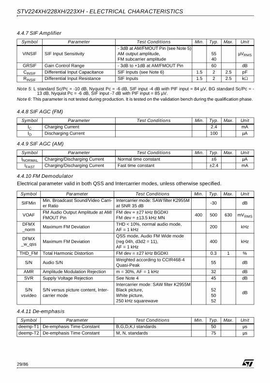
STV224XH/228XH/223XH - ELECTRICAL CHARACTERISTICS
4.4.7 SIF Amplifier
Note 5: L standard Sc/Pc = -10 dB, Nyquist Pc = -6 dB, SIF input -4 dB with PIF input = 84 µV, BG standard Sc/Pc = -13 dB, Nyquist Pc = -6 dB, SIF input -7 dB with PIF input = 85 µV.
Note 6: This parameter is not tested during production. It is tested on the validation bench during the qualification phase.
4.4.8 SIF AGC (FM)
4.4.9 SIF AGC (AM)
4.4.10 FM DemodulatorElectrical parameter valid in both QSS and Intercarrier modes, unless otherwise specified.
4.4.11 De-emphasis
Symbol Parameter Test Conditions Min. Typ. Max. Unit
VINSIF SIF Input Sensitivity- 3dB at AM/FMOUT Pin (see Note 5)AM output amplitude,FM subcarrier amplitude
5540
µVRMS
GRSIF Gain Control Range - 3dB to +1dB at AM/FMOUT Pin 60 dB
CINSIF Differential Input Capacitance SIF Inputs (see Note 6) 1.5 2 2.5 pFRINSIF Differential Input Resistance SIF Inputs 1.5 2 2.5 k�
Symbol Parameter Test Conditions Min. Typ. Max. UnitIC Charging Current 2.4 mA
ID Discharging Current 100 µA
Symbol Parameter Test Conditions Min. Typ. Max. UnitINORMAL Charging/Discharging Current Normal time constant ±6 µA
IFAST Charging/Discharging Current Fast time constant ±2.4 mA
Symbol Parameter Test Conditions Min. Typ. Max. Unit
SIFMinMin. Broadcast Sound/Video Carri-er Ratio
Intercarrier mode: SAW filter K2955M at SNR 35 dB
-30 dB
VOAFFM Audio Output Amplitude at AM/FMOUT Pin
FM dev = ±27 kHz BGDKIFM dev = ±13.5 kHz MN
400 500 630 mVRMS
DFMX_norm
Maximum FM DeviationTHD < 10%, normal audio mode,AF = 1 kHz
200 kHz
DFMX_w_qss
Maximum FM DeviationQSS mode, Audio FM Wide mode(reg 04h, d3d2 = 11),AF = 1 kHz
400 kHz
THD_FM Total Harmonic Distortion FM dev = ±27 kHz BGDKI 0.3 1 %
S/N Audio S/NWeighted according to CCIR468-4 Quasi-Peak
55 dB
AMR Amplitude Modulation Rejection m = 30%, AF = 1 kHz 32 dB
SVR Supply Voltage Rejection See Note 4 45 dB
S/Nvsvideo
S/N versus picture content, Inter-carrier mode
Intercarrier mode: SAW filter K2955MBlack picture,White picture,250 kHz squarewave
525052
dB
Symbol Parameter Test Conditions Min. Typ. Max. Unitdeemp-T1 De-emphasis Time Constant B,G,D,K,I standards 50 µs
deemp-T2 De-emphasis Time Constant M, N, standards 75 µs
29/86

STV224XH/228XH/223XH - ELECTRICAL CHARACTERISTICS
4.4.12 AM Demodulator
4.4.13 SIF Output (AM/FM or Sound Subcarriers Output)
4.4.14 SAW Filter Switch Output (TQFP64 only)
4.4.15 External Audio Input
4.4.16 Main Audio Output (See Figure 17 on page 42 and Figure 18 on page 42)
Symbol Parameter Test Conditions Min. Typ. Max. Unit
AFOUTAM Audio Output Amplitude at AM/FMOUT Pin
54% modulation 400 500 630 mVRMS
AMlowco Low Cut-off Frequency -3 dB compared AFout 40 HzAMhighco High Cut-off Frequency -3 dB compared AFout 30 kHz
AMthd Total Harmonic Distortion 54% modulation 2 %
AMs/n Signal/Noise RatioWeighted according to CCIR468-4 Quasi-Peak
55 dB
AMsvr Supply Voltage Rejection See Note 4 20 dB
Symbol Parameter Test Conditions Min. Typ. Max. UnitSIFout Output Level Sound subcarriers 150 mVRMS
SIFbw Bandwidth Sound subcarriers 7.5 MHz
SIF dcout DC Output Level 4 V
SIFres Residual CarrierFundamental wave (38.9 MHz) and harmonics
0.4 mVRMS
SIFcur Sink Output CurrentAM or FM demod. output selectedSound subcarriers output selected
0.51.5
mA
Symbol Parameter Test Conditions Min. Typ Max. UnitSAW low Low Output Voltage ISINK = 2 mA 0.4 V
SAWcur Maximum allowed Current 2 mASAW high High Output Voltage ISOURCE = 2 mA 4 V
Symbol Parameter Test Conditions Min. Typ. Max. UnitRIN Input Resistance 70 100 130 k�
VIDC DC Input Voltage 2.4 VAFIN maximum Audio Input Signal 2 VRMS
Symbol Parameter Test Conditions Min. Typ. Max. Unit
AMax Maximum Attenuation (Audio Out/AM-FM Out) Register 05hex, data = 7Fhex 78 dB
AMin Minimum Attenuation (Audio Out/AM-FM Out)
VIN = 1 VRMS, f = 1 kHz,Register 05hex, data = 00hex
-1 0 1 dB
ASTEP Step Resolution reg 05, d7 = 0 0.7 dB
DCSH DC Output Shift From max. volume to min. volume 50 mV
VODC DC Output Level 4 V
AFDIFF Audio Amplitude difference between sources
f = 1 kHz, fM = ±27 kHz,Ext. Audio Input = 500 mVRMS
2 dB
ROUT Output Resistance 110 �
BWO Output Bandwidth 1 MHz
THD_AM Total Harmonic Distortion VIN = 1 VRMS, f = 1 kHz 0.1 0.3 %
30/86

STV224XH/228XH/223XH - ELECTRICAL CHARACTERISTICS
Note 7: Measured from any input to output at f = 10 kHz with RL = 10k��and Rg = 600�, Volume attenuation = 0dB.
4.4.17 AVL
4.5 CVBS, Y/C, RGB INPUTS AND CVBS OUTPUTS
4.5.1 Luminance & CVBS Inputs
4.5.2 Combined Chrominance & SVHS Selection Input
4.5.3 CVBS1 Output (Pin 29 - SDIP56)
S/N1 Signal to Noise Ratio from Exter-nal Input
Measured at 0 dB attenuation,Ext. Audio Input at 500 mVRMS,CCIR 468-4 Weighted Quasi Peak
75 dB
S/N2 Signal to Noise Ratio from Exter-nal Input
Measured at 20 dB attenuation,0 dB reference Ext. Audio Input at 500 mVRMS
55 60 dB
S/N3 Signal to Noise Ratio from FM Demod
Measured at 20 dB attenuation,FM: ± 27 kHz (Standards BGDKI) 52 55 dB
SVRV Supply Voltage Rejection from External Input
Measured at f = 100 Hz from VCC = 5 V and VCC = 8 V 60 dB
XT Crosstalk See Note 7 70 dB
NOISE Output Noise Level
CCIR 468-4 Weighted Quasi PeakVolume at minimumVolume at typicalVolume at maximum
5050100
6060120
µV
AFIN Audio Input Level Volume = -25 dB, THD < 1% 2 VRMS
Symbol Parameter Test Conditions Min. Typ. Max. Unit
Symbol Parameter Test Conditions Min. Typ. Max. Unit
GAVLAVL Gain Control Range(7-bit Resolution)
20 dB
AVLMAX Maximum attenuation -15 dB
Reg.AVL Regulation amplitudeMeasured at AUDIOOUTVolume Control at maximum
0.55 VRMS
Symbol Parameter Test Conditions Min. Typ. Max. UnitDCIN1 Black Level Voltage Input selected on main CVBS output 3.3 V
VIN CVBS or Y Input Voltage 1 1.41 VPP
-I Negative Clamping Current During SYNC pulse 20 27 35 µA
I Positive Clamping Current 2.5 4.5 7 µA
Symbol Parameter Test Conditions Min. Typ. Max. Unit
V Chrominance Input Voltage Burst Amplitude, 100/75 Color Bar 0.3 0.6 VPP
VCLIP Input Amplitude before Clipping 1 VPP
VDC DC Voltage SVHS Mode 1.55 1.70 1.85 V
VTH SVHS Threshold Voltage 0.50 0.90 1.45 V
ILOW Output Current 0V at CHR Pin 150 µA
Symbol Parameter Test Conditions Min. Typ. Max. UnitVOUT Dynamic Output Amplitude Register 1Dhex, data = 07hex 1.5 VPP
RLOAD Output Load Resistance Register 1Dhex, data = 07hex 3 k�
BW CVBS BandwidthRegister 1Dhex, data = 07hexVIN = 1 VPP
10 MHz
31/86

STV224XH/228XH/223XH - ELECTRICAL CHARACTERISTICS
4.5.4 CVBS2 Output
4.5.5 OSD RGB Inputs
4.5.6 FBOSD/HC Inputs
Crosstalk Deletion of non-selected signalsRegister 1Dhex, data = 07hexUp to 5 MHz
50 dB
MGAIN Output GainRegister 1Dhex, data = 07hexFrom any CVBS/Y inputs
-0.5 0 0.5 dB
DCMAIN DC Output VoltageRegister 1Dhex, data = 07hexBlack Level
4.2 V
Symbol Parameter Test Conditions Min. Typ. Max. Unit
Symbol Parameter Test Conditions Min. Typ. Max. UnitVOUT2 Dynamic Output Amplitude 3 VPP
ROUT2 Internal Output Resistance 10 �
BW2 CVBS Bandwidth VIN = 1 VPP 10 MHz
Crosstalk2 Deletion of non-selected signals Up to 5 MHz 50 dB
SWI2gain Output Gain From any CVBS/Y inputs 5.5 6 6.5 dB
SWI2DC DC Output Voltage Black Level 3.8 V
RLOAD2 Output Load Resistance 1.5 k�
Symbol Parameter Test Conditions Min. Typ. Max. UnitVCLAMP Clamp Level Max. Contrast 4 VVRGB RGB Input Voltage 0.7 1 VPP
CRGB RGB Gain Max. Contrast, Max. Drive 4.28 -
DblackDifference of black level of internal and external signals at the RGB out-puts
OSD signal versus internal signal 50 mV
IRGB Clamping Current 60 100 140 µACrosstalk Deletion of non-selected RGB source From 0 to 5 MHz 50 dB
Symbol Parameter Test Conditions Min. Typ. Max. Unit
VTHFB1A OSD Insertion Threshold Voltage Half Contrast disableRegister 08hex d6 = 0 0.5 0.7 0.85 V
VTHFB1B OSD Insertion Threshold Voltage Half Contrast enableRegister 08hex d6 = 1 1.5 1.9 2.3 V
VTH-HC Half Contrast Threshold Voltage Half Contrast enableRegister 08hex d6 = 1 0.5 0.7 0.85 V
VTHFB2 Blanking Threshold Voltage, Oversize Blanking activeRegister 08hex, d7 = 1 3.2 4 4.8 V
tSWI1 Insertion Switching Delay 20 40 ns
tSWI2 Blanking Switching DelayFrom FBOSD = 4V to starting of blanking falling edge at RGB out-puts
100 ns
IFB Input current 0V at Pin FBOSD 10 µA
32/86

STV224XH/228XH/223XH - ELECTRICAL CHARACTERISTICS
4.5.7 External RGB/YCrCb Inputs
4.5.8 External Fast Blanking Input (See Note 8)
Note 8: The FBEXT input must be connected to ground if not used in the application.
4.6 LUMA PART
4.6.1 Y Delay Line
4.6.2 Peaking CircuitElectrical parameter measured with color identified
Symbol Parameter Test Conditions Min. Typ. Max. UnitVCLAMP Clamp Level Max. Contrast 3.5 V
VRGB RGB Input Voltage 0.7 1 VPP
VYCrCb YCrCb Input Voltage
100% color barregister 0Ahex d7d6 = 11
YCrCb
10.70.7
VPP
CRGB RGB Gain Max. Contrast, Max. Drive 4.28 -
DblackDifference of black level of internal and external signals at the RGB out-puts
OSD signal versus internal signal 50 mV
IRGB Clamping Current 60 100 140 µA
Crosstalk Deletion of non-selected RGB source From 0 to 5 MHz 50 dB
Symbol Parameter Test Conditions Min. Typ. Max. UnitVTHFB Insertion Threshold Voltage 0.5 0.7 0.85 V
tSWI Insertion Switching Delay 20 40 nsIFB Input Current 0V at Pin FBEXT 10 µA
VMAX Max. voltage allowed at FBEXT input 5 V
Symbol Parameter Test Conditions Min. Typ. Max. UnittD1 Delay Time PAL/NTSC SVHS mode, Register 1F d3 = 0 520 ns
tD2 Delay Time SECAM SVHS mode, Register 1F d3 = 0 640 ns
tD3 Delay Time PAL/NTSC CVBS mode, Register 1F d3 = 0 560 nstD4 Delay Time SECAM CVBS mode, Register 1F d3 = 0 710 ns
tSHIFT Delay Time (lumDel1 - lumDel2)
lumDel1 = reg 1F d3 = 0, standard luma delaylumDel2 = reg 1F d3 = 1, shifted luma delay
140 ns
Groupdel Group Delay up to 3.5MHz Trap-off ±30 ns
Symbol Parameter Test Conditions Min. Typ. Max. UnitfPEAK Center Frequency Trap-off, coring ON 2.5 3 3.5 MHz
GPEAKGain Variation from Min. to Max. peaking
At fPEAK, coring ON 9 dB
OvershootAmplitude Variation compared to B/W amplitude
2T pulse, Max. peaking, coring ON 55 %
33/86

STV224XH/228XH/223XH - ELECTRICAL CHARACTERISTICS
4.6.3 Black Stretch Control (Pin BS) See Figure 12
4.6.4 Y Output
4.7 FILTERS
4.7.1 Y Trap Filter
4.7.2 Chrominance Bandpass
Pre-shootAmplitude Variation compared to B/W amplitude
2T pulse, Max. peaking, coring ON 40 %
Aft-shootAmplitude Variation compared to B/W amplitude
2T pulse, Max. peaking, coring ON 40 %
Coring Coring Range compared to B/W Coring ON 10 %
Symbol Parameter Test Conditions Min. Typ. Max. Unit
Symbol Parameter Test Conditions Min. Typ. Max. Unit
BSth1Black Stretch Threshold referred to B/W amplitude
Y/CVBS inputs: 0.7V B/W, No set-up 50 %
BSMax.Maximum expansion referred toB/W amplitude
Y/CVBS inputs: 0.7V B/W, No set-up -15 %
BSVMax. Black Stretch Control Voltage Max. black stretch 2.6 V
BSVMin. Black Stretch Control Voltage No black stretch 3.3 V
I100IRE Discharging current Y = 100IRE 8 µAI0IRE Charging Current Y = 0IRE 35 µA
Symbol Parameter Test Conditions Min. Typ. Max. UnitYout-DC Black level 3.7 VBW
Yout-amp Black to White Amplitude 0.7 0.99 V
Yout-BW Luma Path Bandwidth
Peaking nominalSVHS mode/Trap-offCVBS, PAL/NTSC 4.43MHzCVBS, SECAMCVBS, PAL/NTSC 3.58MHz
82.72.52.5
3.53.13.0
MHz
Yout S/N Signal to Noise Ratio (VPP/VRMS)Bandwidth 5MHz, Peaking Min.,coring ON
50 dB
Symbol Parameter Test Conditions Min. Typ. Max. UnitfTRAP-PN Notch Frequency PAL/NTSC fOSC MHz
fTRAP-S Notch FrequenciesSECAM fnbSECAM fnr
4.24.5
MHz
fTRAP-ACC Notch Frequency Accuracy 3.5 %
QTRAP Trap Quality FactorQ = 1/ (f0/f-3dB - f-3dB/f0), Peaking Min.
1.5 -
CrejPN Color Subcarrier Rejection PAL/NTSC 20 dB
CrejS Color Rejection in SECAM ModeFrom 4.1 to 4.6 MHzAt 3.9 MHz 10
20dB
Symbol Parameter Test Conditions Min. Typ. Max. UnitfBP Center Frequency Register 12h, d3-d0 = 0000 -5% fOSC +5% MHz
QBP Bandpass Quality Factor 2.8 3.5 4.2 -
34/86

STV224XH/228XH/223XH - ELECTRICAL CHARACTERISTICS
4.7.3 Bell Filter
4.8 CHROMA PART
4.8.1 ACC
4.8.2 ACC Overload
4.8.3 Killer
4.8.4 Chroma PLL
4.8.5 PLL Loop Filter (PAL/NTSC)
4.8.6 Hue Control
4.8.7 Automatic Flesh Control
Symbol Parameter Test Conditions Min. Typ. Max. UnitfBELL Center Frequency Register 11h, d4-d0 = 00000 4.27 4.29 4.31 MHz
QBP Bell Quality Factor 14 16 18 -
Symbol Parameter Test Conditions Min. Typ. Max. Unit
GACC ACC Control RangeChange of burst overall ACC control range < 2dB
26 dB
VMin. Minimum Burst Signal Amplitude Within the ACC control range 0.03 VPP
Symbol Parameter Test Conditions Min. Typ. Max. UnitVTH Chroma regulation Threshold ACC overload ON, PAL/NTSC 3 dB
Symbol Parameter Test Conditions Min. Typ. Max. Unit
Ident-kill Color on Threshold of ident. circuit Burst amplitude on selected CVBS input 5 mVPP
Kill-Hyst Color off Killer Hysteresis Strong signal condition, S/N > 40 dB 2 mVPP
Symbol Parameter Test Conditions Min. Typ. Max. Unit
CaptR Catching Range With recommended crystal and rec-ommended CLPF filter value. ±300
HoldR Holding Range > or = to capture range
Symbol Parameter Test Conditions Min. Typ. Max. Unit
IC Maximum Control Current Color search mode (colour not ident.)Color identified
1000350 µA
IL Leakage Current 5 µA
Frange-W Auto Flesh Control Register 14(HEX), d6 = 1, d7 = 1 ±90 Deg
Symbol Parameter Test Conditions Min. Typ. Max. UnitRHUE Hue Control Range ±35 ±45 ±55 Deg
Symbol Parameter Test Conditions Min. Typ. Max. UnitFleshNom. Nominal Flesh Tint Phase 118 Deg
Fcorr0 Phase Correction when Auto Flesh ON At FleshNom 0 Deg
FMax.-N Maximum Phase Correction Register 14(HEX), d6 = 1, d7 = 0 ±10 Deg
Flesh-N Chroma Input Phase at Max. cor-rection Register 14(HEX), d6 = 1, d7 = 0 ±30 Deg
Frange-N Auto Flesh Control Range Register 14(HEX), d6 = 1, d7 = 0 ±60 Deg
35/86

STV224XH/228XH/223XH - ELECTRICAL CHARACTERISTICS
4.8.8 Color Demodulators
4.8.9 Chroma Delay Line
4.8.10 Chroma Reference Output
4.9 SCANNING PART
4.9.1 Synchronization Separator
4.9.2 Horizontal Oscillator
FMax.-W Maximum Phase Correction Register 14(HEX), d6 = 1, d7 = 1 ±20 Deg
Flesh-W Chroma Input Phase at Max. cor-rection Register 14(HEX), d6 = 1, d7 = 1 ±45 Deg
Frange-W Auto Flesh Control Register 14(HEX), d6 = 1, d7 = 1 ±90 Deg
Symbol Parameter Test Conditions Min. Typ. Max. Unit
Symbol Parameter Test Conditions Min. Typ. Max. UnitDoffsetP Demodulator Offset PAL/NTSC mode, 75% color bar ±2 %
DoffsetS Demodulator Offset SECAM mode, 75% color bar ±2 %PhaseErr Phase Error in demodulated signal PAL/NTSC mode, 90% matrix 5 Deg
TransPal Chroma Transient Time PAL mode, 75% color bar green-magenta transient 700 ns
transSEC Chroma Transient Time SECAM mode, 75% color bar green-magenta transient 900 ns
Naxis R-Y Demodulation Axis NTSC mode, 104° matrix 104 Deg
Symbol Parameter Test Conditions Min. Typ. Max. UnitCdelay Delay of delayed signals Relative to non delayed signal 63.9 64 64.1 µs
CtransDifference of transient times be-tween delayed and non delayed signals
SECAM mode. tRN -tRN+1tRN: rise time line N (direct)tRN+1: rise time line N +1 (delayed)
150 ns
DgainDifferential Gain of delayed signals versus direct signals
SECAM mode. Gn+1/GnGn: direct channel gainGn+1: delayed channel gain
-0.5 0 0.5 dB
Symbol Parameter Test Conditions Min. Typ. Max. Unit
CHR-amp Chroma VCO Reference Signal Amplitude 0.4 VPP
ISCHR Sink Current 0.5 mA
Symbol Parameter Test Conditions Min. Typ. Max. UnitVSYNC Synchronization Pulse Amplitude 50 300 450 mV
Symbol Parameter Test Conditions Min. Typ. Max. UnitfH50 Horizontal Frequency 50 Hz mode 15.6 kHz
fH60 Horizontal Frequency 60 Hz mode 15.7 kHz
fRANGE Frequency Control RangeLow FrequencyHigh Frequency
14.715.9
15.016.3
15.3—
kHz
fFREE Free Frequency when PLL1 opened 15.3 15.6 15.9 kHz
36/86

STV224XH/228XH/223XH - ELECTRICAL CHARACTERISTICS
4.9.3 First Loop Filter
4.9.4 Second Loop Filter
Note 9: This parameter is not tested during production, it is tested during the qualification phase.
4.9.5 Line Flyback Input/Super-Sandcastle Output
4.9.6 Horizontal Output
4.9.7 Vertical Output
Symbol Parameter Test Conditions Min. Typ. Max. UnitILOW Long Time Constant Output Current 0.10 0.13 0.16 mA
IHIGH Short Time Constant Output Current 0.30 0.40 0.56 mA
IVLOW Very Long Time Constant 0.03 0.05 0.07 mA
Symbol Parameter Test Conditions Min. Typ. Max. Unit
CrangeP2 Control Range from start of horizon-tal output to flyback pulse Centered horizontal position 0 to
12 µs
HSHIFT Horizontal Position Control Range 5 5.25 µs
HDRIFT Horizontal Drift with temperature From 0°C to 70°C (see Note 9) 200 ns
Symbol Parameter Test Conditions Min. Typ. Max. UnitVBURST Output Voltage during Burst Key 4.8 5.3 5.8 V
VLINEClamped Input Voltage during Line Flyback
2.6 3 3.4 V
VVERT Output Voltage during Vertical pulse 1.8 2 2.2 V
Twbg Burst key Pulse Width 3.8 µs
TdbgDelay of start of burst key to start of sync.
5.2 µs
Tvert Vertical Pulse Width 10.5 lines
VTHLINEPLL2 and Line Blanking Threshold Voltage referred to line level Vline
Vthline/Vline 83 %
I Input Current 0.1 1 mA
Symbol Parameter Test Conditions Min. Typ. Max. UnittW Output Pulse Width 26 28 30 µs
VLOW Low Output Voltage ISINK = 5mA 0.4 V
VCCSTART VCC Start Level 5.5 6 6.5 VVCCSTOP VCC Stop Level Hysteresis VCCSTART - VCCSTOP 0.5 0.6 0.7 V
IMax. Maximum allowed Output Current 10 mA
VMax. Maximum allowed Output Voltage 10 V
TssOutput Pulse Duty Cycle in soft-start mode (tHIGH/(tHIGH+tLOW)
75 %
Symbol Parameter Test Conditions Min. Typ. Max. UnittW Output Pulse Width 10.5 Lines
VLOW Low Output VoltageReg 19, d0 = 1Reg 19, d0 = 0
1.5 20.1
2.50.5
V
fLOCK Looking Range 248 352 LinesfFREE-50 Free Frequency (no Video signal) 50-Hz Forced or 50-Hz Auto mode 314 Lines
fFREE-60 Free Frequency (no Video signal) 60-Hz Forced or 60-Hz Auto mode 264 Lines
37/86

STV224XH/228XH/223XH - ELECTRICAL CHARACTERISTICS
4.9.8 Vertical Amplitude Control
4.9.9 Crystal Detection
4.10 RGB CONTROL PART
4.10.1 Y Input
4.10.2 U & V Inputs
4.10.3 Contrast Control
4.10.4 Saturation Control
VHIGHHigh Level Range Vertical Position Control
Min. position controlMax. position control
3.56.0
46.5
4.57.0
V
ISINK Output Sinking Current 0.7 1.0 mAISOURCE Output Source Current 0.7 1.0 mA
Symbol Parameter Test Conditions Min. Typ. Max. Unit
Symbol Parameter Test Conditions Min. Typ. Max. Unit
VAMP Output Voltage RangeMin. amplitude voltageMax. amplitude voltage
1.25.5
1.56.0
1.76.5
V
Symbol Parameter Test Conditions Min. Typ. Max. UnitR4.43 Load resistance at pin VAMP 4.43 MHz crystal on pin XTAL1 80 k�
R3.58 Load resistance at pin VAMP 3.58 MHz crystal on pin XTAL1 10 k�
Symbol Parameter Test Conditions Min. Typ. Max. UnitYINdc Black Level 3.7 V
Yin-B/W Black to White Amplitude 0.7 1 V
Yin-cur Input Current 1 µA
Symbol Parameter Test Conditions Min. Typ. Max. UnitUVin-dc Black Level 3.7 VUin-amp B-Y Amplitude 75% color bar PAL/SECAM 1.33 2.0 VPP
Vin-amp R-Y Amplitude 75% color bar PAL/SECAM 1.05 2.0 VPP
UVin-cur Input Current 1 µA
Symbol Parameter Test Conditions Min. Typ. Max. UnitYctr Contrast Range on Y signal 21 24 27 dB
OSDctrContrast Range on OSD RGB sig-nal
10 12 14 dB
Symbol Parameter Test Conditions Min. Typ. Max. Unit
SATMax. Maximum Saturation Control75% color bar PAL/SECAM, 0 dB for data 20 in reg 08
6 9 12 dB
SATMin. Minimum Saturation Control75% color bar PAL/SECAM, 0 dB for data 20 in reg 08
-40 dB
38/86

STV224XH/228XH/223XH - ELECTRICAL CHARACTERISTICS
4.10.5 Brightness Control
4.10.6 RGB Matrix
4.10.7 Drive Adjustment (White Point Adjustment)
4.10.8 Cut-Off Adjustment (Black Point Adjustment)
4.10.9 Cathode Current Input
4.10.10 Beam Current Limiter InputSee Figure 14 on page 42 and Figure 15 on page 42.
Symbol Parameter Test Conditions Min. Typ. Max. Unit
BrightBrightness Control Range referred to B/W amplitude on RGB outputs
At Max. Contrast, APR OFF 50 60 70 %
Blacknom
Nominal Black Level at RGB out-puts. Difference between black lev-el VBLACK and inserted cut-off pulse level VCO: VBLACK - VCO
BS mode, Max. Contrast. (VBLACK - VCO)/V_BWV_BW: black to white amplitude at RGB outputs.
-12 %
Symbol Parameter Test Conditions Min. Typ. Max. Unit
G/R (G-Y)/(R-Y)PAL/SECAM matrix measured on R, G outputs PAL DEMpattern
-0.40 -0.51 -0.62 -
G/B (G-Y)/(B-Y)PAL/SECAM matrix measured on G, B outputs PAL DEMpattern
-0.15 -0.19 -0.23 -
R/Bntsc (R-Y)/(B-Y)NTSC mode, 104° matrix input signal: U = V measured on R, B outputs
0.9 -
G/Rntsc (G-Y)/(R-Y) NTSC mode, 104° matrix -0.29 -
G/Bntsc (G-Y)/(B-Y) NTSC mode, 104° matrix -0.22 -
Symbol Parameter Test Conditions Min. Typ. Max. UnitWPrange White Point Adjustment Range On RGB outputs 6 dB
Symbol Parameter Test Conditions Min. Typ. Max. Unit
COadjust Cut-off Adjustment RangeOn Red and green outputs at Typ. drive, no load
420 mV
COloop Cut-off Loop Range On RGB outputs 2 2.5 V
COlevel Inserted Cut-off Level 1.5 2.5 3.5 V
Symbol Parameter Test Conditions Min. Typ. Max. Unit
VLEAKLeakage Current Reference Volt-age
3.75 4 V
VCOFF
Cut-off Current Reference Voltage referred to leakage current refer-ence VLEAK
210 250 290 mV
VSBEAMStart Beam Current Detection Ref-erence Voltage
4.1 4.3 V
ISOURCE Source Current 150 µA
Symbol Parameter Test Conditions Min. Typ. Max. UnitVTH1 Contrast Attenuation Starting 5.75 V
VTH2 Brightness Attenuation Starting 5.5 VVTH3 Contrast Attenuation Ending 5.25 V
CTRbcl Contrast Attenuation at VTH3 14 dB
VTH4 Brightness Attenuation Ending 4.5 V
39/86

STV224XH/228XH/223XH - ELECTRICAL CHARACTERISTICS
4.10.11 Automatic RGB Peak Regulation (APR) / RGB Peak LimitationSee Figure 16 on page 42.
Note 10: At maximum contrast, APR and RGB peak limitation have the same characteristics. The APR regulation levelis tracked on contrast. The RGB peak limitation level is not tracked on contrast.
BRIGbcl Brightness Attenuation at VTH4 100 %
Clp High Clamping Voltage 6.5 VSAF-thr Safety Threshold 0.8 1 1.2 V
SAF-hold Supply Hold Voltage Referred to VCC1 3 V
Symbol Parameter Test Conditions Min. Typ. Max. Unit
APR/RGB Peak
Maximum Output Level on RGB outputs when APR/RGB Peak Limi-tation ON
WR10 d0 = 1Contrast Max., drive Max., no load APR threshold Min. (50IRE)APR threshold 70IREAPR threshold Max. (100IRE) (see Note 10)
2.143.0
4.28
V
iAPR-D Discharging Current 5.5 µAiAPR-C Charging Current 5.25 mA
GAPRMAX APR max gain
APR ON = WR10 d0 = 1RGB output amplitude with APR ON versus RGB output amplitude with APR OFF
+2.5 dB
GAPRMIN APR min gain
APR ON = WR10 d0 = 1RGB output amplitude with APR ON versus RGB output amplitude with APR OFF
-3.0 dB
Symbol Parameter Test Conditions Min. Typ. Max. Unit
40/86

STV224XH/228XH/223XH - ELECTRICAL CHARACTERISTICS
4.10.12 RGB Outputs
Figure 12. Black Stretch Static Characteristics (IRE)
Figure 13. Auto Flesh Characteristics
Symbol Parameter Test Conditions Min. Typ. Max. Unit
VB/W Output Signal Amplitude B/W0.7V B/W on Y/CVBS inputs, Contrast Max., Drive Max., Saturation and bright Nom., APR OFF, no load
2.8 V
VBLUE Output Signal Amplitude75/100 color bar, no Y nom. settings, APR OFF, no load
1.5 VPP
ISINK Output Sinking Current 1.2 1.5 mAISOURCE Output Source Current 1.8 mA
ROUT Internal Output Resistance 150 �
VBLANK Blanking Level No load 0.2 0.4 VVCLIP High Clipping Level No load 6.8 V
Black-ctr Variation of black level with contrast 30 mV
Black-satVariation of black level with satura-tion
50 mV
Rel-BlackRelative Variation in black level be-tween the three channels
20dB contrast variationOverall brightness range±5% VCC1
20 mV
Black-T Black Level Thermal Drift 1 mV/°C
TrackTracking between Luminance and Chrominance signals
At typical saturationFrom Max. Contrast (0 dB) to -10 dB Contrast
2 dB
Bwidth Bandwidth of output signals at -3dBYUV inputs to RGB outputsOSD RGB inputs to RGB outputsEXT. RGB inputs to RGB outputs
665
886
MHz
100
-15
0
50
50 100
YOUT (%)
YIN (%)
-20
-10
0
10
20Phase Correction (Deg)
0 90 210 24060 15030 120 180
Chroma InputPhase (Deg)
NarrowResponse
Wide Response
41/86

STV224XH/228XH/223XH - ELECTRICAL CHARACTERISTICS
Figure 14. Beam Current Limiter Characteristics (Contrast)
Figure 15. Beam Current Limiter Characteristics (Brightness)
Figure 16. Automatic RGB Peak Regulation (APR) / RGB Peak Limitation Characteristics
Figure 17. Linear Volume Control Curve(7 bits, reg. 05 d6-d0, reg. 05 d7 = 0)
Figure 18. Non-Linear Volume Control Curve (6 bits, reg. 05 d6-d1, reg. 05 d7 = 1)
4.5 5 5.5 6 6.5
0
-12
-18
-24
-6
VBCL (V)
Contrast (dB)
-6dB
-10dB
-18dB
0dB Max.
4.5 5 5.5 6 6.50
50
100
VBCL (V)
Brightness (%)
0 50 100 150
Output Level
Input Level (IRE)
APR Threshold max. (100 IRE)and contrast max.
APR Threshold min. (50 IRE)and contrast max.
APR Threshold max. (100 IRE)and contrast min.
APR Threshold min. (50 IRE)and contrast min.
RGB Peak Limitation Curve or
0
-20
-40
-60
-800 15050 100
Code (decimal)
Vol
ume
Co
ntro
l Atte
nuat
ion
(d
B) 0
-20
-40
-60
-800 10 70
Code (decimal)
Vol
ume
Con
trol
Atte
nua
tion
(dB
)
30 5020 40 60
42/86

STV224XH/228XH/223XH - ELECTRICAL CHARACTERISTICS
4.11 I²C BUS CHARACTERISTICS
4.11.1 SCL
4.11.2 SDA
4.11.3 I²C Timing
Figure 19. I²C Bus Timing
Symbol Parameter Test Conditions Min. Typ. Max. UnitVIL Low Level Input Voltage -0.5 1.5 V
VIH High Level Input Voltage 3 VCC+0.5 V
ILI Input Leakage Current VIN = 0 to VCC -10 10 µAfSCL Clock Frequency 0 100 kHz
tR Input Rise Time 1.5V to 3V 1.000 ns
tF Input Fall Time 1.5V to 3V 300 nsCI Input Capacitance 10 pF
Symbol Parameter Test Conditions Min. Typ. Max. UnitVIL Low Level input Voltage -0.5 1.5 V
VIH High Level input Voltage 3 VCC+0.5 VILI Input Leakage Current VIN = 0 to VCC -10 10 µA
CI Input Capacitance 10 pF
tR Input Rise Time 1.5V to 3V 1.000 nstF Input Fall Time 1.5V to 3V 300 ns
VOL Low Level Output Voltage IOL = 3mA 0.4 V
tF Output Fall Time 3V to 1.5V 250 nsCL Load Capacitance 400 pF
CI Input Capacitance 10 pF
Symbol Parameter Test Conditions Min. Typ. Max. UnittLOW Clock Low period 4.7 µstHIGH Clock High period 4 µs
tSU,DAT Data Set-up Time 250 ns
tHD,DAT Data Hold Time 0 340 ns
tSU,STOSet-up Time from Clock High to Stop
4 µs
tBUF Start Set-up Time following a Stop 4.7 µs
tHD,STA Start Hold Time 4 µs
tSU,STAStart Set-up Time following Clock Low to High Transition
4.7 µs
tBUF
tLOW
tHIGHtHD,STA tR tF
tSU,STA
tHD,DAT
tSU,DAT
tSU,STO
SDA
SCL
SDA
43/86

STV224XH/228XH/223XH - I²C BUS SPECIFICATIONS
5 I²C BUS SPECIFICATIONSData transfers follow the usual I²C format: after the start condition (S), a 7-bit slave address is sent, fol-lowed by an eighth bit which is a data direction bit (W). An 8-bit sub-address is sent to select a register, fol-lowed by an 8-bit data word to be included in the register.
The IC’s I²C bus decoder permits the automatic incrementation mode in write mode.
The circuit operates up to clock frequencies of 400 kHz.
String FormatWrite only mode (S = start condition, P = stop condition, A = acknowledge)
Read only mode
Slave Address
S SLAVE ADDRESS 0 A SUB-ADDRESS A DATA A P
S SLAVE ADDRESS 1 A DATA 0 A DATA 1 A DATA 2 A DATA 3 A P
Address A7 A6 A5 A4 A3 A2 A1 A0
Value 1 0 0 0 1 0 1 X
Write Address: 10001010Read Address: 10001011
44/86

STV224XH/228XH/223XH - I²C BUS SELECTION
6 I²C BUS SELECTION
6.1 SUMMARY INPUT SIGNALS (WRITE MODE)
“Not-to-be-used” data must be set to “0”.
Reg.Addr.(Hex)
Data D7 Data D6 Data D5 Data D4 Data D3 Data D2 Data D1 Data D0
00 PIFVCO Free Running Fine AdjustmentNot to
be used
01PIF
Over-modu-lation
AFCDefeat
L/L’ ModeNEG/POSModulation
PIFVCO Free Running Coarse Adjustment
02CVBS Out-
putOvermodu-lation Reset
Not to be used
INTCVBS Output Amplitude Adjustment
03 Tuner AGC gain Tuner AGC Starting Point Adjustment
04IntercarrierFilter ON/
OFF
QSS and AM demod defeat
FM/AM Output
Selection (Note 1)
FM Demod. Defeat
FM Deviation and FMDe-emphasis, Audio FM
Wide mode (Note 1)
Main Audio Outputselection (int./ext.)
05Volume Control Curve
Volume Control
06Not to be
usedQSS/
Inter-carrierCVBS Mute
Not to be used
(SDIP56)
SAW FilterSwitch
(TQFP64)
AGC SIF Time Con-
stant
Sound Standard Selection
PIF VCOcompensa-
tion
07 Blue ScreenRGB Peak Limitation (Note 2)
Contrast
08Oversize Blanking
Half Contrast
Saturation
09 CO Blanking RGB
BlankingBrightness
0ARGBext/YCrCb Insertion
(Note 2)Red Drive Adjustment
0BNTSC Set-
upBlack
StretchGreen Drive Adjustment
0CLSB RED
Cut-off Counter
CO Freeze Blue Drive Adjustment
0D Manual Cut-off Selection Red Cut-off Adjustment
0ELSB GREEN
Cut-off Counter
Not to be used
Green Cut-off Adjustment
0FWhite inser-tion ON/OFF
CVBS2ON/OFF
Chroma Trap ON/
OFF (Note 1)
CoringON/OFF
Peaking
10White
Insertion (Note 2)
CRT/LCDDisplay
RGBosdContrast Selection
APR Threshold APR on/off
45/86

STV224XH/228XH/223XH - I²C BUS SELECTION
Note 1: Specification changed versus STV223XD/224XC.Note 2: New feature versus STV223XD/224XC.
6.2 SUMMARY OUTPUT SIGNALS (READ MODE)
11ACCO
ON/OFFNTSC 104
Matrix
PAL/NTSC Demod.
GainBell Filter Shift
12 Not to be usedChroma DL
ON/OFFChroma Out
ON/OFFBandpass Shift
13 Not to be usedCrystal In-
put Pin Disa-ble
Chroma Standard Selec-tion
Crystal Selection 3rd Crystal
14 Flesh Char.Flesh
ON/OFFHue
15 Safety Reset Not to be used SVHS switchSecond Video Switch Con-
trolMain Video
Switch Control
16 InterlaceHOUTDisable
Horizontal Shift
17 50/60Hz Selection Vertical Amplitude
18Vertical Sync
ON/OFF
Line Sync ON/OFF
PLL1 Time Constant Vertical Position
19
AV ModeTime
Constant(Note 2)
CopyProtection
Mode(Note 2)
Wide LineBlanking(Note 2)
Not to be Used
Noise Detector Threshold
Long Blanking
Vertical Output Low
Level Control
1A Manual Cut-off Register - Red
1B Manual Cut-off Register - Green1C Manual Cut-off Register - Blue
1D CVBS1out
1E Not to be usedAGC SIF
Time Constant
Not to be used
1FAudio Out
(Mono or Soundsubcarriers)
AVLLuma Delay
ShiftNot to be
used
SoundStatus
Refresh
VERT Out-put Inhibition
Reg. Addr.(Hex)
Data D7 Data D6 Data D5 Data D4 Data D3 Data D2 Data D1 Data D0
00Chroma Standard Selection Status
Crystal Selection StatusVideo Ident.
StatusField Lock
Status50/60 Hz
StatusPower ON
Reset
01FM Dem.VCO Cal.
Status
Scanning VCO Cal.
Status
TestNot to be
Used
FBext De-tection
SafetyStatus
Horizontal Lock Status
Noise Detec-tor Status
SVHSStatus
02 Cut-off loop status FM Sound Carrier Levels Digital AF Status
03
Tuner AGC Output Sta-tus or AVL Gain Status
IC Identification
Reg.Addr.(Hex)
Data D7 Data D6 Data D5 Data D4 Data D3 Data D2 Data D1 Data D0
46/86

STV224XH/228XH/223XH - I²C BUS SELECTION
6.3 INPUT SIGNALS (WRITE MODE)
Not used data bits must be set to “0”.
6.3.1 PIFVCO Free Running
6.3.2 PIF Free Running Coarse
6.3.3 PIF Features
Reg.Addr.(Hex)
Description BitsData
Commentsd7 d6 d5 d4 d3 d2 d1 d0
00 PIFVCO Free RunningFine Adjustment
7 011
001
001
001
001
001
001
XXX
PIF Typical + 0.7 MHz.PIF Free Running mid range.PIF Typical - 0.7 MHz.
Not to be used 1 X X X X X X X 0
Reg.Addr.(Hex)
Description BitsData
Commentsd7 d6 d5 d4 d3 d2 d1 d0
01 PIFVCO Free Running CoarseAdjustment for 38.9 MHz Carrier
4XXX
XXX
000
XXX
001
011
011
011
PIFVCO = F0 + 2.0 MHz.PIFVCO = F0 (mid range).PIFVCO = F0 - 1.8 MHz.
PIFVCO Free Running CoarseAdjustment for 33.9 MHz Carrier (L’)
4XXX
XXX
111
111
001
011
011
011
PIFVCO = F0 + 1.3 MHz.PIFVCO = F0 (mid range).PIFVCO = F0 - 1.2 MHz.
PIF Modulation1 X
XXX
XX
01
XX
XX
XX
XX
0 = Negative Modulation.1 = Positive Modulation.
L/L’ StandardSelection
1 XX
XX
01
11
XX
XX
XX
XX
0 = L Standard.1 = L’ Standard.
Digital AFC Defeat1 X
X01
XX
XX
XX
XX
XX
XX
0 = AFC Active.1 = AFC Defeat (read register 02, d2 d1 d0 = 000).
PIF Over-modulation
1 01
XX
XX
XX
XX
XX
XX
XX
0 = Over-modulation detection off.1 = Over-modulation regulation active.
Reg.Addr.(Hex)
Description BitsData
Commentsd7 d6 d5 d4 d3 d2 d1 d0
02CVBS Output Ampli-tude
5 XXX
XXX
XXX
011
001
001
001
001
VTyp. - 1.6 dB.VTyp. = 1.6 V (black / white).VTyp.+ 1.5 dB.
Not to be used 1 X X 0 X X X X X
Overmodulation Reset
1 XX
01
XX
XX
XX
XX
XX
XX
0 = Normal Operating Mode
1 = Overmodulation Reset
CVBS Output1 0
1XX
XX
XX
XX
XX
XX
XX
0 = 2 VPP, no external sound trap.1 = 2.3 VPP, external sound trap.
47/86

STV224XH/228XH/223XH - I²C BUS SELECTION
6.3.4 Tuner Delay
6.3.5 SIF Features and Audio Switches
Reg.Addr.(Hex)
Description BitsData
Commentsd7 d6 d5 d4 d3 d2 d1 d0
03Tuner AGC Starting Point Adjustment
6 XXX
XXX
011
001
001
001
001
001
Min. Start point 2 mVRMS at PIF input.Typ. Start point 12 mVRMS at PIF input.Max. Start point 80 mVRMS at PIF input
Tuner AGC Gain
2 0011
0101
XXXX
XXXX
XXXX
XXXX
XXXX
XXXX
50 µA/dB.95 µA/dB.170 µA/dB.270 µA/dB.
Reg. Addr(Hex)
Description BitsData
Commentsd7 d6 d5 d4 d3 d2 d1 d0
04Main Audio Output
2 XXX
XXX
XXX
XXX
XXX
XXX
001
01X
FM/AM audio selected.External audio selected.MUTE selected.
FM De-emphasis Switch and FM de-viation range con-trol
2XXXX
XXXX
XXXX
XXXX
0011
0101
XXXX
XXXX
Automatic control, according to sound standard.De-emphasis at 75 µs and FM deviation at �25 kHz.De-emphasis at 50 µs and FM deviation at �50 kHz.Audio FM Wide mode &50 µs De-emphasis (BGDKI).To be used with 224xH version only in QSS architec-ture.
FM Demodulator defeat
1 XX
XX
XX
01
XX
XX
XX
XX
0 = FM Demodulator active.1 = FM Demodulator defeat, FM out muted.
AM/FM output se-lection
1 XX
XX
01
XX
XX
XX
XX
XX
0 = FM output selected.1 = AM output selected and FM demod OFF.
QSS and AM de-modulator defeat
1XX
01
XX
XX
XX
XX
XX
XX
0 = QSS and AM demod active, 1 = QSS and AM demod not active (OFF)
Intercarrier filter ON/OFF
101
XX
XX
XX
XX
XX
XX
XX
0 = Intercarrier filter ON1 = Intercarrier filter OFF
05 Volume Control Attenuation,Linear curve (dB)
7 00
01
01
01
01
01
01
01
Attenuation = 0 dB.Attenuation = 78 dB.7-bit resolution.
Volume Control Attenuation,Non-linear curve(d0 = 0, d7 = 1)
6 11
01
01
01
01
01
01
00
Attenuation = 0 dB.Attenuation = 78 dB.6-bit resolution.
48/86

STV224XH/228XH/223XH - I²C BUS SELECTION
6.3.6 Video Controls
06 PIF VCO Compen-sation
1XX
XX
XX
XX
XX
XX
XX
01
0 = Optimized for PIF from 33.9 to 38.9 MHz1 = Optimized for PIF 45.75 & 58.75 MHz
Sound Standard Selection
2 XXXX
XXXX
XXXX
XXXX
XXXX
0011
0101
XXXX
6.5 MHz sound selected.6.0 MHz sound selected.5.5 MHz sound selected.4.5 MHz sound selected.
AGC SIF time constant (AM)
1 XX
XX
XX
XX
01
XX
XX
XX
0 = Auto Time constant.1 = Fast Time constant forced.
SAW filter switch output
1 XX
XX
XX
01
XX
XX
XX
XX
0 = output low (0.4 V Max.).1 = output high (4 V Min.).
CVBS output(from PIF circuit)
1XX
XX
01
XX
XX
XX
XX
XX
0 = CVBS output enable.1 = CVBS output muted.
QSS/Inter-carrier Application
1XX
01
XX
XX
XX
XX
XX
XX
0 = QSS application, intercarrier filter OFF1 = Intercarrier application
Not to be used 1 0 X X X X X X X
Reg. Addr(Hex)
Description BitsData
Commentsd7 d6 d5 d4 d3 d2 d1 d0
Reg. Addr(Hex)
Description BitsData
Commentsd7 d6 d5 d4 d3 d2 d1 d0
07 Contrast Control
6 XX
XX
01
01
01
01
01
01
-24 dB gain (Min. contrast).0 dB gain (Max. contrast).
RGB Peak Limitation
1 XX
01
XX
XX
XX
XX
XX
XX
0 = APR, APR Threshold, tracked with contrast.1 = RGB Peak Limitation, threshold not tracked with contrast.
Note: RGB Peak Limitation active when WR10 d0 = 1
Blue Screen Feature
1 01
XX
XX
XX
XX
XX
XX
XX
0 = Blue screen OFF.1 = Blue screen ON.
08Saturation Control
6 XX
XX
01
01
01
01
01
01
-40 dB gain (Min. saturation).+9 dB gain (Max. saturation).
Half Contrast Ena-ble
1 XX
01
XX
XX
XX
XX
XX
XX
0 = Disabled.1 = Enabled.
Oversize Blanking Enable
1 01
XX
XX
XX
XX
XX
XX
XX
0 = Disabled.1 = Enabled.
09Brightness Control
6 XX
XX
01
01
01
01
01
01
-30% of B/W at Max. contrast.+30% of B/W at Max. contrast.
RGB Blanking1 X
X01
XX
XX
XX
XX
XX
XX
0 = Not active (normal operation).1 = Active.
Cut-off Blanking
1 0
1
X
X
X
X
X
X
X
X
X
X
X
X
X
X
0 = Enable: RGB output blanked when ICATH voltage is far from internal cut-off reference (cut-off loop not locked), during IC start-up.1 = Disable: RGB output not blanked by cut-off loop.
49/86

STV224XH/228XH/223XH - I²C BUS SELECTION
0A Red Drive Adjust (White Point R)
6 XX
XX
01
01
01
01
01
01
-6 dB gain (Min. drive).0 dB gain (Max. drive).
RGBext/YCrCbSelection
2 0
011
0
101
X
XXX
X
XXX
X
XXX
X
XXX
X
XXX
X
XXX
RGB ext. insertion enable controlled by FBext input pin.RGB ext. insertion disable, FBext control disable.RGB ext. insertion forced (FBext not active).YCrCb insertion forced.if WR0F d5 = 0 : Y on Gext (Luminance input) and CVBSin (for synchro).if WR0F d5 = 1 : Y on CVBSin (for luminance and synchro), Cr on Rext, trap and luma delay disabled.
0B Green drive adjust-ment (white point G)
6 XX
XX
01
01
01
01
01
01
-6 dB gain (Min. drive).0 dB gain (Max. drive).
Black stretch ena-ble
1 XX
01
XX
XX
XX
XX
XX
XX
0 = Black stretch disable.1 = Black stretch enable.
Black Stretch Reference Level
101
XX
XX
XX
XX
XX
XX
XX
0 = 0 IRE (no set-up).1 = 7.5 IRE (NTSC set-up).
0C Blue drive adjust-ment (white point B)
6 XX
XX
01
01
01
01
01
01
-6 dB gain (Min. drive).0 dB gain (Max. drive).
Cut-off loop control1 X
X01
XX
XX
XX
XX
XX
XX
0 = Cut-off loop active.1 = Cut-off loop frozen.
LSB (9th bit) Red cut-off counter
101
XX
XX
XX
XX
XX
XX
XX
Red LSB = 0Red LSB = 1
0D Red cut-off adjust-ment (Black point R)
6 XX
XX
01
01
01
01
01
01
-150 mV.+150 mV.
Manual Cut-off Se-lection
2 0
1
0
1
X
X
X
X
X
X
X
X
X
X
X
X
Automatic Cut-off application, data = 00hex in registers 1A,1B, 1C.Manual cut-off application DC at R,G,B output are adjusted thanks registers 1A, 1B, 1C.
01
10
XX
XX
XX
XX
XX
XX
Not allowed.Not allowed.
0E Green cut-off ad-justment (Black point G)
6 XX
XX
01
01
01
01
01
01
-150 mV.+150 mV.
Not to be used 1 X 0 X X X X X X
LSB (9th bit) Green cut-off counter
101
XX
XX
XX
XX
XX
XX
XX
Green LSB = 0Green LSB = 1
0F Peaking Control 4 XX
XX
XX
XX
01
01
01
01
0 dB at center Freq. Min. peaking.+ 6dB at center Freq.Max. peaking.
Coring on sharp-ness
1 XX
XX
XX
01
XX
XX
XX
XX
0 = Coring off.1 = Coring on.
Chroma Trap and Luma Delay Selec-tion
1 XX
XX
01
XX
XX
XX
XX
XX
0 = Trap and Luma Delay Enabled.1 = Trap and Luma Delay Disabled.
CVBS2 ON/OFF 1 XX
01
XX
XX
XX
XX
XX
XX
0 = CVBS2 output Enabled.1 = CVBS2 output Disabled.
White Insertion 1 01
XX
XX
XX
XX
XX
XX
XX
0 = White insertion not active.1 = White insertion enable during HOUT soft mode.
Reg. Addr(Hex)
Description BitsData
Commentsd7 d6 d5 d4 d3 d2 d1 d0
50/86

STV224XH/228XH/223XH - I²C BUS SELECTION
6.3.7 Chroma Controls
10 APR Enable1 X
XXX
XX
XX
XX
XX
XX
01
0 = APR disable.1 = APR enable.Note: WR10 d0 to be set to 1 when RGB peak limi-tation is used
APR Threshold 4 XX
XX
XX
01
01
01
01
XX
50 IRE.100 IRE.
RGB OSD Con-trast Selection
1 XX
XX
01
XX
XX
XX
XX
XX
0 = Contrast control disable.1 = Contrast control enable.
CRT/LCD Display 1 XX
01
XX
XX
XX
XX
XX
XX
0 = RGB output blanking active, CRT Display1 = RGB output blanking replaced by black level, LCD Display
White Insertion 1 01
XX
XX
XX
XX
XX
XX
XX
White Insertion controlled by WR0Fd7White forced at RGB Output
Reg. Addr(Hex)
Description BitsData
Commentsd7 d6 d5 d4 d3 d2 d1 d0
Reg.Addr.(Hex)
Description BitsData
Commentsd7 d6 d5 d4 d3 d2 d1 d0
11Bell Filter Adjust
5 XX
XX
XX
01
01
01
01
01
0 kHz.+100 kHz.
PAL/NTSCDemodulation Gain
1 XX
XX
01
XX
XX
XX
XX
XX
0 = 0 dB gain (nominal).1 = +6 dB gain.
NTSC Matrix 1XX
01
XX
XX
XX
XX
XX
XX
0 = 90° matrix selection.1 = 104° matrix selection (in NTSC only).
ACC Overload Disable 101
XX
XX
XX
XX
XX
XX
XX
0 = ACC overload active.1 = ACC overload disable.
12Bandpass adjust
4 XX
XX
XX
XX
01
01
01
01
f = fosc.f = 1.1*fosc.
Chroma reference out-put
1 XX
XX
XX
01
XX
XX
XX
XX
0 = Chroma reference output OFF.1 = Chroma reference output ON.
Chroma DL selection1 X
XXX
01
XX
XX
XX
XX
XX
0 = ON.1 = OFF.
Not to be used 2 0 0 X X X X X X
13
Crystal Selection
2 XXXX
XXXX
XXXX
XXXX
XXXX
0011
0101
XXXX
XTAL1 (4.43/3.5XX MHz).XTAL2 (3.5XX MHz).XTAL3 (3.5XX MHz).Not allowed.
Standard Selection
2 XXXXXXX
XXXXXXX
XXXXXXX
001111X
010001X
XX001X1
XX010X1
XX0XXXX
PAL.NTSC.SECAM (only with XTAL1).Not allowed.Not allowed.AUTO mode.Not allowed
Crystal Inhibition
2 XXXX
XXXX
0011
XXXX
XXXX
XXXX
XXXX
0101
Two-crystal, P/S/N application.Three-crystal, P/N application.One-crystal, P/S/N 4.43 MHz application.Two-crystal, P/N application.
Not to be used 2 0 0 X X X X X X
51/86

STV224XH/228XH/223XH - I²C BUS SELECTION
6.3.8 Scanning Controls
14 Hue Control (in NTSC only)
6 XX
XX
01
01
01
01
01
01
-45°.+45°.
Flesh Enable1 X
X01
XX
XX
XX
XX
XX
XX
0 = Flesh disable (OFF).1 = Flesh enable (ON).
Wide Flesh Charac-Teristic Selection
1 01
XX
XX
XX
XX
XX
XX
XX
0 = Normal characteristic.1 = Wide characteristic.
15 Main Video Switch
2 XXX
XXX
XXX
XXX
XXX
XXX
001
01X
CVBS1 selected.CVBS2 selected.Y/CVBS3 selected.
Second Video Switch Control
2 XXXX
XXXX
XXXX
XXXX
0011
0101
XXXX
XXXX
CVBS1 selected.CVBS2 selected.Y/CVBS3 selected.Y+C selected.
SVHS Switch Chroma Decoder Input Selec-tion
1 XX
XX
XX
01
XX
XX
XX
XX
0 = Main CVBS selected.1 = CHR input selected (SVHS).
Not to be used 2 X 0 0 X X X X X
Safety Reset1 0
1XX
XX
XX
XX
XX
XX
XX
0 = Safety active1 = Reset Safety, Safety non-active
Reg.Addr.(Hex)
Description BitsData
Commentsd7 d6 d5 d4 d3 d2 d1 d0
Reg.Addr.(Hex)
Description BitsData
Commentsd7 d6 d5 d4 d3 d2 d1 d0
16 Horizontal Shift
6 XX
XX
01
01
01
01
01
01
-2.5 µs.+2.5 µs.
Horizontal Output Pulse Disable
1 XX
01
XX
XX
XX
XX
XX
XX
0 = Normal mode.1 = HOUT disable (high level).
Interlace1 0
1XX
XX
XX
XX
XX
XX
XX
0 = Interlace mode.1 = De-interlace mode.
17Vertical Amplitude 6
XX
XX
01
01
01
01
01
01
1.5 V on VAMP Pin.6.0 V on VAMP Pin.
50/60Hz Selection 2
0011
0101
XXXX
XXXX
XXXX
XXXX
XXXX
XXXX
Auto (50 Hz when no ident.).60 Hz.50 Hz.Auto (60 Hz when no ident.).
18Vertical Position
4 XX
XX
XX
XX
01
01
01
01
4 V high level on VERT Pin.6 V high level on VERT Pin.
PLL1 Time Constant
2 XXXX
XXXX
0011
0101
XXXX
XXXX
XXXX
XXXX
Auto time constant selection.Short time constant.Long time constant.Very long time constant.
Horizontal Synchronization
1 XX
01
XX
XX
XX
XX
XX
XX
0 = PLL1 active.1 = PLL1 not active (horiz. free running mode).
Vertical Synchronization
1 01
XX
XX
XX
XX
XX
XX
XX
0 = Vertical synchronization active.1 = Vertical free running mode.
52/86

STV224XH/228XH/223XH - I²C BUS SELECTION
6.3.9 Miscellaneous
19 Vertical Output Low Level Control
1 XX
XX
XX
XX
XX
XX
XX
01
0 = 0.1 V low level on VERT Pin.1 = 2 V low level on VERT Pin.
Frame Blanking1 X
XXX
XX
XX
XX
XX
01
XX
0 = Adapted to standard.1 = Long blanking (50 Hz blanking) both in 50 Hz and 60 Hz modes
Noise Detector Threshold
2 XX
XX
XX
XX
01
01
XX
XX
Low threshold.High threshold.
Not to be used 1 X X 0 0 X X X X
Wide Line Blanking 1XX
XX
01
XX
XX
XX
XX
XX
0 = Standard Line Blanking1 = Wide Line Blanking
Copy Protection Mode1 X
X01
XX
XX
XX
XX
XX
XX
0 = Normal PLL1 operating mode.1 = Copy Protection Mode.
AV Mode TimeConstant
1 01
XX
XX
XX
XX
XX
XX
XX
0 = PLL1 short time constant during all frames.1 = PLL1 long time constant during vertical blank-ing, short time constant for the rest of the field.
Reg.Addr.(Hex)
Description BitsData
Commentsd7 d6 d5 d4 d3 d2 d1 d0
Reg. Addr.(Hex)
Description BitsData
Commentsd7 d6 d5 d4 d3 d2 d1 d0
1A Manual Cut-offRegister Red
801
01
01
01
01
01
01
01
Low DC at RGB output.High DC at RGB output.
1B Manual Cut-offRegister Green
801
01
01
01
01
01
01
01
Low DC at RGB output.High DC at RGB output.
1C Manual Cut-offRegister Blue
801
01
01
01
01
01
01
01
Low DC at RGB output.High DC at RGB output.
1D CVBS1 Out selection at pin 29 SDIP56 8
00
00
00
00
00
10
10
10
CVBSOUT1 selected at pin 29 SDIP56. Default value, set to 0h when CVBSOUT1 not used.
1E Not To Be Used 7 0 0 0 X 0 0 0 0
SIF AGC time constant (positive mod-ulation)
100
00
00
01
00
00
00
00
Automatic SIFAGC Time constant control.Forced Long time constant.
53/86

STV224XH/228XH/223XH - I²C BUS SELECTION
6.4 OUTPUT SIGNALS (READ MODE)
1FVERT Output Inhibition
1 XX
XX
XX
XX
XX
00
XX
01
VERT normal operating.VERT inhibition (forced to high DC level controlled by vertical position register).
Sound Level Status Refresh
1 XX
XX
XX
XX
XX
00
01
XX
0 = Sound level status continuously refreshed1 = Sound level status refreshed only at the end of vertical synchronization pulse
Not to be used 1 X X X X X 0 X X
Luma Delay Shift1 X
XXX
XX
XX
01
00
XX
XX
Standard luma delay.140 ns on luma delay.
AVL Control & Status
2 XXXX
XXXX
0011
0101
XXXX
XXXX
XXXX
XXXX
AVL OFF, read reg 03h, d7 = AGC Tuner StatusAVL OFF, read reg 03h, d7 = AGC Tuner StatusAVL ON, read reg 03h, d7 = AVL Gain StatusAVL ON, read reg 03h, d7 = AGC Tuner Statusreg 04h, d3d2 = 11: AVL Gain Status = 1 (Min.)reg 04h, d3d2 � 11: AVL Gain Status = 0 (Max.)
AM/FMOUT pin selec-tion
2 0011
0101
XXXX
XXXX
XXXX
0000
XXXX
XXXX
Output of AM/FM demodulator.Sound subcarriers selected.Audio output muted.Main audio switch output, either internal or exter-nal audio depending on main audio switch selec-tion. reg 04h; d0 = 0: internal audio. reg 04h; d0 = 1: external audio.
Reg. Addr.(Hex)
Description BitsData
Commentsd7 d6 d5 d4 d3 d2 d1 d0
Reg.
Addr.(Hex)
Description BitsData
Commentsd7 d6 d5 d4 d3 d2 d1 d0
00Power-on Reset
1 XX
XX
XX
XX
XX
XX
XX
01
Normal mode.Power down mode.
Field Frequency1 X
XXX
XX
XX
XX
XX
01
XX
50 Hz.60 Hz.
Field Lock Status1 X
XXX
XX
XX
XX
01
XX
XX
Not locked.Locked.
Video Identification1 X
XXX
XX
XX
01
XX
XX
XX
No identification.Video identification.
Standard Status Crystal Selection
2 XXXX
XXXX
0011
0101
XXXX
XXXX
XXXX
XXXX
XTAL1 (4.43 MHz).XTAL2 (3.5X MHz).XTAL3 (3.5X MHz).XTAL1 (3.5X MHz).
Standard Selection
2 0011
0101
XXXX
XXXX
XXXX
XXXX
XXXX
XXXX
PAL.NTSC.SECAM.COLOR OFF.
54/86

STV224XH/228XH/223XH - I²C BUS SELECTION
01SVHS status
1 XX
XX
XX
XX
XX
XX
XX
01
No SVHS (CVBS mode).SVHS mode.
Noise detection1 X
XXX
XX
XX
XX
XX
01
XX
High S/N.Low S/N.
Scanning Horizontal phase-locked loop status
1 XX
XX
XX
XX
XX
01
XX
XX
Not locked.Locked.
Safety status1 X
XXX
XX
XX
01
XX
XX
XX
Safety not active.Safety active.
Fast Blanking detection on external fast blanking pin
1 XX
XX
XX
01
XX
XX
XX
XX
No insertion detected.Insertion on FBext.
Test1 X
XXX
01
XX
XX
XX
XX
XX
Not to be used
Scanning VCO Calibration
1 XX
01
XX
XX
XX
XX
XX
XX
Not calibrated.Calibrated.
FM demodulation VCO calibration
1 01
XX
XX
XX
XX
XX
XX
XX
Not calibrated.Calibrated.
02
Digital AFC status
3 XXXXX
XXXXX
XXXXX
XXXXX
XXXXX
00011
11000
10001
FPLL - F0 < -300 kHz.-300 kHz < FPLL - F0 < -60 kHz.-60 kHz < FPLL - F0 < +60 kHz.+60 kHz < FPLL- F0 < +300 kHz.+300 kHz < FPLL - F0.
Sound carrier level
3 XXXXXXXX
XXXXXXXX
00001111
00111100
01100110
XXXXXXXX
XXXXXXXX
XXXXXXXX
Level 1 (low sound carrier signal).Level 2.Level 3.Level 4.Level 5.Level 6.Level 7.Level 8 (high sound carrier signal)
Blue cut-off register and cut-off loop status
2 001
1
010
1
XXX
X
XXX
X
XXX
X
XXX
X
XXX
X
XXX
X
Blue CO register < 011110000Blue CO register > 100001111011110000 < Blue CO register < 100001111 and Icath not locked011110000 < Blue CO register < 100001111 and Icath locked
03IC identification
1 XX
XX
XX
XX
XX
XX
XX
01
TQFP64SDIP56
Tuner AGC Output Status(reg 1Fh, d5d4 = 00 or 01 or 11)
1 01
XX
XX
XX
XX
XX
XX
XX
Tuner AGC Output not activeTuner AGC Output active
AVL Gain Status (reg 1Fh, d5d4 = 10)
1 01
XX
XX
XX
XX
XX
XX
XX
AVL Gain Max. (Low audio signal)AVL Gain Min. (High audio signal)
Reg.
Addr.(Hex)
Description BitsData
Commentsd7 d6 d5 d4 d3 d2 d1 d0
55/86

STV224XH/228XH/223XH - I²C BUS SELECTION
6.5 POWER-ON RESET - INITIAL BUS REGISTER CONDITIONS
Power-On Reset is active when the power supply VCCD is below 3 Volts.
All data from all registers must be written by microprocessor after power-on. Unused data must be set to0. POR values are not tested during production.
Reg.Addr.(Hex)
Initial Data ValueComments
d7 d6 d5 d4 d3 d2 d1 d0
00 1 0 0 0 0 0 0 0 PIFVCO free running fine adjustment Typical.
01 0 0 0 0 0 1 1 1PIFVCO coarse typ, BG = 38.9 MHz, Negative modulation, AFC active, no PIF over-modulation regulation.
02 0 0 0 1 0 0 0 0 CVBS amplitude Typical, 2VPP.
03 0 0 1 0 0 0 0 0 Tuner AGC starting point Typical, Tuner AGC gain Min.
04 0 0 0 0 0 0 0 0FM/AM out selected, FM de-emphasis and FM deviation auto-control, FM demod. active, FM out selected, QSS and AM demod. active.
05 0 1 1 1 1 1 1 1 Volume control attenuation at maximum, linear curve (dB).
06 0 0 0 0 0 0 0 0PIF < 42 MHz, 6.5 MHz sound carrier selected, auto AGC SIF time constant, saw filter switch control at low level, CVBS out enabled, QSS mode.
07 0 0 1 0 0 0 0 0 Contrast at middle, blue screen disabled.
08 0 0 1 0 0 0 0 0 Saturation at middle, half contrast disabled, oversize blanking disabled.
09 0 0 1 0 0 0 0 0 Brightness at middle, RGB Blanking not active.0A 0 0 1 0 0 0 0 0 Red drive at middle, RGBext insertion enabled (FBext Pin control).
0B 0 0 1 0 0 0 0 0 Green drive at middle, black stretch disabled, black stretch ref 0IRE.
0C 0 0 1 0 0 0 0 0 Blue drive at middle, cut-off loop active.0D 0 0 1 0 0 0 0 0 Red cut-off at middle, automatic cut-off loop.
0E 0 0 1 0 0 0 0 0 Green cut-off at middle.
0F 0 0 0 0 1 0 0 0Peaking on luma at middle, coring off, trap ON (CVBS & color identified), CVBS2 ON, white insertion not active.
10 0 0 0 1 0 0 0 0 APR disabled, APR threshold at middle, RGB OSD contrast disabled.
11 0 0 0 0 0 0 0 0No shift of bell filter center frequency, 0dB P/N demod. gain, 90° matrix selection, ACC overload ON.
12 0 0 0 0 0 0 0 0No shift of bandpass center frequency, chroma reference output off, chroma delay line on.
13 0 0 0 0 0 0 0 0 Two crystals application P/S/N, PAL XTAL1 forced mode, two crystal applications.14 0 0 1 0 0 0 0 0 Hue at middle, flesh disabled, normal flesh characteristic.
15 0 0 0 0 0 0 0 0CVBS1 selected on main CVBS output, CVBS1 selected on second CVBS output, CVBS mode.
16 0 0 1 0 0 0 0 0 Horizontal shift at middle, horizontal output enabled, interlace mode.
17 0 0 1 0 0 0 0 0 Vertical amplitude at middle, auto 50/60 Hz identification.
18 0 0 0 0 1 0 0 0Vertical position at middle, automatic time constant selection on PLL1, PLL1 active, Vertical synchronization active.
19 0 0 0 0 0 0 0 00.1 V low level at pin VERT, frame blanking adapted to standard, noise detector low threshold.
1A 0 0 0 0 0 0 0 0 Not active, auto cut-off.
1B 0 0 0 0 0 0 0 0 Not active, auto cut-off.1C 0 0 0 0 0 0 0 0 Not active, auto cut-off.
1D 0 0 0 0 0 0 0 0 R-Y output at pin 29 (SDIP56)
1E 0 0 0 0 0 0 0 0 Not to be used, except d4: Auto. SIF AGC time constant control in L/L’ standards.1F 0 0 0 0 0 0 0 0 VERT pulse active, standard luma delay, AVL off, AM/FM mono sound selected.
56/86

STV224XH/228XH/223XH - I²C BUS SPECIFICATION COMPATIBILITY
7 I²C BUS SPECIFICATION COMPATIBILITYThe STV2246H/36H, 2286H, 2247H/37H, 2248H/38H and 2249H/39H I²C bus specification is com-patible between IC version. However, some dedi-cated settings must be used for the different ver-
sions. The following sections show the differencesbetween the various versions. An “X” means thatthe function is available and can be set to “1” or“0”.
Note 1: The FBEXT pin must be connected to ground.
CAUTION: The specification of WR04 d3:2 has changed.For 224XC versions (refer to STV224XC datasheet), WR04 d3:2 = 11 (bin.) means that FM demod de-emphasis is bypassed. This function is used for BTSC application compatibility.
For 224XD/XE versions, WR04 d3:2 = 11: NOT TO BE USED.
For 224XH versions, WR04 d3:2 = 11 (bin.) means that Audio FM Wide mode is selected and it must beused in QSS applications only. In this case, the following registers must be programmed:
WR04 d3:2 = 11 (bin.) (Audio FM Wide mode)
WR06 d6 = 0 (QSS application)
WR1F d5:4 = 1x (bin.) (AVL ON)
CAUTION: The specification of WR07 d6 has changed.For 224XC/224XD versions, WR07 d6 = 1 means “insertion of cut-off pulses after a vertical oversizeblanking”
For 224XE/XH versions, WR07 d6 = 1 means “RGB peak limitation”
CAUTION: The specification of WR0F d5 has changed.The new specification is:
WR0F d5 = 0: trap and luma delay active; this is not changed
WR0F d5 = 1: trap and luma delay disabled (bypass); this is changed
2248H/38H 2249H/39H 2247H/37H 2246H/36H 2286HRGBext
WR0A d7:6X X X X 011
L/L' modeWR01 d5
X 0 0 0 0
Positive/Negative ModulationWR01 d4
X 0 0 0 0
FM/AM Output SelectionWR04 d5
X 0 0 0 0
Bell FilterWR11 d4:0
X X 00000 00000 00000
QSS/Intercarrier ApplicationWR06 d6
X X X 1 1
QSS and AM defeatWR04 d6
X X X 1 1
AGC SIF Time ConstantWR06 d3 & WR1E d4
X X X X 00
CVBSout amplitudeWR02 d4:0
X X X X 10000
57/86

STV224XH/228XH/223XH - INPUT/OUTPUT SCHEMATIC DIAGRAMS
8 INPUT/OUTPUT SCHEMATIC DIAGRAMS
Figure 20. Ground and Supply Voltages
Figure 21. Main Audio Output
VCCD (5 V)Pin 53 (SDIP56)
VCCIF (5 V)Pin 12 (SDIP56)
VCC2 (8 V)Pin 17 (SDIP56)
VCC1 (8 V)Pin 45 (SDIP56)
GNDDPin 54 (SDIP56)
GNDIFPin 10 (SDIP56)
GND2Pin 19 (SDIP56)
GND1Pin 43 (SDIP56)
VCC2 (8V)
GNDIFGNDIF GNDIFGNDIF
50 �AUDIOOUTPin 55 (SDIP56)
58/86

STV224XH/228XH/223XH - INPUT/OUTPUT SCHEMATIC DIAGRAMS
Figure 22. Scanning PLL Filter
SLPFPin 50 (SDIP56)
GND1
VREF
VCC1
VCC1
VCC1(8 V)
VCC1
59/86

STV224XH/228XH/223XH - INPUT/OUTPUT SCHEMATIC DIAGRAMS
Figure 23. I²C Bus Data Input
Figure 24. I²C Bus Clock Input
VCCD (5V)
GNDD
GNDD
GNDD
5 V
10 k�
SDAPin 52 (SDIP56)
VCCD (5V)
GNDD
GNDD
10 k�
5 V
SCLPin 51 (SDIP56)
60/86

STV224XH/228XH/223XH - INPUT/OUTPUT SCHEMATIC DIAGRAMS
Figure 25. FM Demodulation Capacitor
Figure 26. IF Inputs
VCCIF (5V)
GNDIF
GNDIF
GNDIF
GNDIF
GNDIF
GNDIFGNDIF
GNDIF
VCCIF (5V)
50 �
FMCAPPin 56 (SDIP56)
VCCIF (5V)
GNDIF
GNDIF
GNDIF
2.5 V
SIFIN1Pin 1 (SDIP56)
PIFIN1Pin 6 (SDIP56)
SIFIN2Pin 2 (SDIP56)PIFIN2Pin 7 (SDIP56)
61/86

STV224XH/228XH/223XH - INPUT/OUTPUT SCHEMATIC DIAGRAMS
Figure 27. AGC SIF Capacitor
Figure 28. Voltage Reference Filtering
VCCIF (5V)
GNDIF
GNDIF
GNDIF
GNDIF
GNDIF
AGCSIFCAPPin 3 (SDIP56)
VCCIF (5V)
GNDIF GNDIF
GNDIF GNDIF
VREFIFPin 4 (SDIP56)
62/86

STV224XH/228XH/223XH - INPUT/OUTPUT SCHEMATIC DIAGRAMS
Figure 29. AGC PIF Capacitor
Figure 30. SAW Filter Switch Output (TQFP64)
VCCIF (5V)
GNDIF
GNDIF GNDIF
GNDIF
GNDIF
GNDIF
GNDIF
GNDIF
AGCPIFCAPPin 5 (SDIP56)
VCCIF (5V) (Pin 20 - TQFP64)
GNDIF
SAWSWI 15(TQFP64)
63/86

STV224XH/228XH/223XH - INPUT/OUTPUT SCHEMATIC DIAGRAMS
Figure 31. AGC Tuner Output
Figure 32. IF PLL Filter
VCCIF (5V)
GNDIF GNDIF GNDIF GNDIF
GNDIF
GNDIF
12 V
TUNERAGCOUTPin 8 (SDIP56)
VCCIF (5V)
GNDIFGNDIF
GNDIF
GNDIF GNDIF
GNDIF
IFPLLPin 9 (SDIP56)
64/86

STV224XH/228XH/223XH - INPUT/OUTPUT SCHEMATIC DIAGRAMS
Figure 33. AM/FM Mono or Stereo Sound Carrier Output
Figure 34. Internal CVBS Output
VCC2 (8V)
GNDIF
GNDIF
AM/FMOUT/SCPin 11 (SDIP56)
VCC2 (8V)
VCCIF (5V)
GNDIF
GNDIF
GNDDGNDIF
INTCVBSOUTPin 13 (SDIP56)
65/86

STV224XH/228XH/223XH - INPUT/OUTPUT SCHEMATIC DIAGRAMS
Figure 35. External Audio Input
Figure 36. PIF LC Inputs
VCCIF (5V)
GNDIF GNDIF
GNDIF
GNDIF
GNDIFEXTAUDINPin 14 (SDIP56)
GNDIF
GNDIF
GNDIF
GNDIF
GNDIF
VCCIF (5 V)
PIFLC1Pin 15 (SDIP56)
PIFLC2Pin 16 (SDIP56)
66/86

STV224XH/228XH/223XH - INPUT/OUTPUT SCHEMATIC DIAGRAMS
Figure 37. CVBS Video Inputs
Figure 38. Black Stretch Capacitor
VCC1 (8 V)
GND2
GND1
GND1 GND1
GND1GND1
CVBSIN1Pin 18 (SDIP56)CVBSIN2Pin 20 (SDIP56)
VCC2 (8 V)
GND2GND2GND2
GND2
BSPin 21 (SDIP56)
67/86

STV224XH/228XH/223XH - INPUT/OUTPUT SCHEMATIC DIAGRAMS
Figure 39. RGB & YCrCb External Video Inputs
Figure 40. External Fast Blanking Input
VCC2 (8 V)
GND2
GND2 GND2GND2 GND2
GND2
BEXT/CBPin 25 (SDIP56)GEXT/YPin 26 (SDIP56)
REXT/CRPin 27 (SDIP56)
VCC2 (8 V)
VCCD (5 V)
GND2 GND2 GND2 GND2
GND2 GND2 GND2 GND2GND2
FBEXTPin 28 (SDIP56)
68/86

STV224XH/228XH/223XH - INPUT/OUTPUT SCHEMATIC DIAGRAMS
Figure 41. Y/CVBS External Input
Figure 42. Chroma (SVHS) Input
VCC1 (8 V)
GND1GND1
GND1GND1
GND1
GND2
GND1
Y/CVBSIN3Pin 22 (SDIP56)
VCC1 (8 V)
GND2
GND1
GND1
GND1
CHRPin 23 (SDIP56)
69/86

STV224XH/228XH/223XH - INPUT/OUTPUT SCHEMATIC DIAGRAMS
Figure 43. Automatic RGB Peak Regulation
Figure 44. RGB Outputs
VCC2 (8 V)
GND2
GND2
GND2
APRPin 24 (SDIP56)
VCC2 (8 V)
GND2 GND2
GND2
GND2
BOUTPin 30 (SDIP56)GOUTPin 31 (SDIP56)
ROUTPin 32 (SDIP56)
70/86

STV224XH/228XH/223XH - INPUT/OUTPUT SCHEMATIC DIAGRAMS
Figure 45. Cathode Current Measurement Input
VCC2 (8 V)
GND2 GND2GND2 GND2
GND2GND2
GND2
ICATHPin 33 (SDIP56)
71/86

STV224XH/228XH/223XH - INPUT/OUTPUT SCHEMATIC DIAGRAMS
Figure 46. OSD RGB Inputs
VCC2 (8 V)
GND2GND2GND2
GND2GND2
GND2
BOSDPin 34 (SDIP56)
GOSDPin 35 (SDIP56)ROSDPin 36 (SDIP56)
72/86

STV224XH/228XH/223XH - INPUT/OUTPUT SCHEMATIC DIAGRAMS
Figure 47. Half Contrast Input
Figure 48. 3.5X MHz Crystal or Bell Filter Tuning Capacitor
VCC2 (8 V)
GND2
GND2
GND2
GND2 GND2
GND2
FBOSD/HCPin 37 (SDIP56)
VCCD (5 V) VCC1 (8 V)
GND1
GND1
GND1
GND1GND1
GND1
GND1
XTAL3/BTUNPin 38 (SDIP56)
73/86

STV224XH/228XH/223XH - INPUT/OUTPUT SCHEMATIC DIAGRAMS
Figure 49. 4.43/3.5X MHz Crystal
Figure 50. Chroma PLL Filter
VCC1 (8 V) VCCD (5 V)
GND1
GND1
GND1
XTAL1Pin 40 (SDIP56)XTAL2Pin 39 (SDIP56)
VCCD (5 V)
VCC1 (8 V)
GND1
GND1 GND1 GND1 GND1 GND1
GND1 GND1
CPLFPin 41 (SDIP56)
74/86

STV224XH/228XH/223XH - INPUT/OUTPUT SCHEMATIC DIAGRAMS
Figure 51. XTAL1 Control Pin, Vert. Amplitude DAC Output and Chroma Reference Signal Output
Figure 52. NTBC or Main CVBS Video Switch Output
VCC1 (8 V)
GND1GND1
GND1 GND1 GND1 GND1
X1/VAMP¨/CHROUTPin 42 (SDIP56)
VCC1 (8 V)
GND1 GND1 GND1
NTBC/CVBSOUT1Pin 29 (SDIP56)
75/86

STV224XH/228XH/223XH - INPUT/OUTPUT SCHEMATIC DIAGRAMS
Figure 53. Second CVBS Video Switch Output
Figure 54. Beam Current Limiter Control Voltage and Safety Input
VCC1 (8 V)
GND1
GND1
GND1 GND1 GND1 GND1
CVBSOUT2Pin 44 (SDIP56)
VCC1 (8 V)
GND1
GND1
GND1
GND1 GND1 GND1GND1BCL/SAFPin 46 (SDIP56)
76/86

STV224XH/228XH/223XH - INPUT/OUTPUT SCHEMATIC DIAGRAMS
Figure 55. Vertical Output Pulse
Figure 56. Horizontal Output Pulse
VCC1 (8 V)
GND1
GND1
GND1
GND1
VERTPin 47 (SDIP56)
VCC1 (8 V)
GND1 GND1
GND1HOUTPin 48 (SDIP56)
77/86

STV224XH/228XH/223XH - INPUT/OUTPUT SCHEMATIC DIAGRAMS
Figure 57. Line Flyback Input and Super-Sandcastle Output
VCC1 (8 V)
GND1
GND1
GND1
GND1 GND1
GND1
GND1
LFB/SSCPin 49 (SDIP56)
78/86

STV224XH/228XH/223XH - APPLICATION DIAGRAMS
9 APPLICATION DIAGRAMS
Figure 58. STV2246H
MU
LTIS
TA
ND
AR
D A
SIA
MO
NO
AP
PLI
CA
TIO
N
PA
L/N
TS
C B
G/D
K/I/
M/N
BG
/DK
/I
27 k
Oh
m1
µF
Au
dio
Ou
t(t
o a
udio
am
plif
ier)
LFB
BC
L
CV
BS
OU
T2
(2V
PP)
FB
OS
D
BO
SD
RO
SD
GO
SD
VA
MP
FM
CA
P
AU
DIO
OU
T
GN
DD
VC
CD
SD
A
SC
L
SL
PF
LF
B/S
SC
HO
UT
VE
RT
BC
L/S
AF
VC
C1
CV
BS
OU
T2
GN
D1
X1
/VA
MP
/CH
RO
UT
CL
PF
XT
AL
1
XT
AL
2
XT
AL
3
RO
SD
GO
SD
BO
SD
I CA
TH
RO
UT
GO
UT
BO
UT
NT
BC
/CV
BS
OU
T1
NC
NC
NC
VR
EF
IF
AG
CP
IFC
AP
PIF
IN1
PIF
IN2
TU
NE
RA
GC
OU
T
IFP
LL
GN
DIF
FM
OU
T
VC
CIF
INT
CV
BS
OU
T
EX
TA
UD
IOIN
PIF
LC
1
PIF
LC
2
VC
C2
CV
BS
IN1
GN
D2
CV
BS
IN2
BS
Y/C
VB
SIN
3
CH
R
AR
R
BE
XT
/Cb
GE
XT
/Y
RE
XT
/Cr
FB
EX
T
INT
CV
BS
OU
T
EX
TE
RN
AL
CV
BS
IN
PU
T
FB
OS
D/H
C
Fro
m E
xt.
RG
B o
rF
rom
Ext
. Y
CrC
b
SV
HS
CV
BS
OU
T1
(1
VP
P)
S T V 2 2 4 6 H
56
kO
hm
s
22
nF
22
nF
22
nF
79/86

STV224XH/228XH/223XH - APPLICATION DIAGRAMS
Figure 59. STV2247H
C4
21
µF
R38
FM
CA
P
AU
DIO
OU
T
GN
DD
VC
CD
SD
A
SC
L
SL
PF
LF
B/S
SC
HO
UT
VE
RT
BC
L/S
AF
VC
C1
CV
BS
OU
T2
GN
D1
X1
/VA
MP
/CH
RO
UT
CL
PF
XT
AL
1
XT
AL
2
XT
AL
3
RO
SD
GO
SD
BO
SD
I CA
TH
RO
UT
GO
UT
BO
UT
NT
BC
/CV
BS
OU
T1
SIF
IN1
SIF
IN2
AG
CS
IFC
AP
VR
EF
IF
AG
CP
IFC
AP
PIF
IN1
PIF
IN2
TU
NE
RA
GC
OU
T
IFP
LL
GN
DIF
FM
OU
T/S
C
VC
CIF
INT
CV
BS
OU
T
EX
TA
UD
IOIN
PIF
LC
1
PIF
LC
2
VC
C2
CV
BS
IN1
GN
D2
CV
BS
IN2
BS
Y/C
VB
SIN
3
CH
R
AR
R
BE
XT
/Cb
GE
XT
/Y
RE
XT
/Cr
FB
EX
T
INT
CV
BS
OU
T
EX
TE
RN
AL
CV
BS
IN
PU
T
LF
B
Au
dio
Ou
t(t
o a
ud
io a
mp
lifie
r)
BC
L
CV
BS
OU
T(2
VP
P)
SD
A
SC
L
FB
OS
D
RO
SD
GO
SD
BO
SD
J3
2T
o C
RT
Bo
ard
ICATH
GND
ROUT
GOUT
BOUT
VCC
FB
OS
D/H
C
MU
LTIS
TA
ND
AR
D A
SIA
ST
ER
EO
AP
PLI
CA
TIO
N
PA
L/N
TS
C B
G/D
K/I/
M/N
S T V 2 2 4 7 H
Fro
m E
xt.
RG
B o
rF
rom
Ex
t. Y
crC
b
SV
HS
CV
BS
OU
T1
(1
VP
P)
27
kO
hm
s
56 k
Oh
ms
22
nF
22
nF
22
nF
80/86

STV224XH/228XH/223XH - APPLICATION DIAGRAMS
Figure 60. STV2248H
BG
/DK
/I/L
BG
/DK
1 µ
F
ICATH
GND
ROUT
GOUT
BOUT
VCC
J32
To
CR
T B
oa
rdFB
OS
D
RO
SD
GO
SD
BO
SD
Au
dio
Ou
t(t
o A
ud
io A
mp
lifie
r)
SC
L
SD
A
LF
B
BC
L
HO
UT
VO
UT
CV
BS
OU
T
VA
MP
FM
CA
P
AU
DIO
OU
T
GN
DD
VC
CD
SD
A
SC
L
SL
PF
LF
B/S
SC
HO
UT
VE
RT
BC
L/S
AF
VC
C1
CV
BS
OU
T2
GN
D1
X1
/VA
MP
/CH
RO
UT
CL
PF
XT
AL
1
XT
AL
2
XT
AL
3/B
TU
N
RO
SD
GO
SD
BO
SD
I CA
TH
RO
UT
GO
UT
BO
UT
SIF
IN1
SIF
IN2
AG
CS
IFC
AP
VR
EF
IF
AG
CP
IFC
AP
PIF
IN1
PIF
IN2
TU
NE
RA
GC
OU
T
IFP
LL
GN
DIF
AM
/FM
OU
T/S
C
VC
CIF
INT
CV
BS
OU
T
EX
TA
UD
IOIN
PIF
LC1
PIF
LC
2
VC
C2
CV
BS
IN1
GN
D2
CV
BS
IN2
BS
Y/C
VB
SIN
3
CH
R
AR
R
BE
XT
/Cb
GE
XT
/Y
RE
XT
/Cr
FB
EX
T
FB
OS
D/H
C
MU
LTI-
ST
AN
DA
RD
EU
RO
PE
AN
AP
PLI
CA
TIO
N
PA
L/S
EC
AM
/NT
SC
BG
/DK
/I/LL
’
S T V 2 2 4 8 H
(2V
PP)
NT
BC
/CV
BS
OU
T1
CV
BS
OU
T1
(1V
PP
)
56
kO
hm
s
22
nF
22
nF
22
nF
81/86

STV224XH/228XH/223XH - APPLICATION DIAGRAMS
Figure 61. STV2238H (TQFP64)
1 µ
F
LF
B/S
SC
HO
UT
VE
RT
BC
L/S
AF
NC
VC
C1
CV
BS
OU
T2
GN
D1
X1
/VA
MP
/CH
RO
UT
CL
PF
XT
AL
1
XT
AL
2
XT
AL
3/B
TU
N
NC
FB
OS
D
RO
SD
IFP
LL
GN
DIF
AM
/FM
OU
T/S
C
VC
CIF
INT
CV
BS
OU
T
EX
TA
UD
IOIN
PIF
LC
1
PIF
LC
2
VC
C2
CV
BS
IN1
GN
D2
CV
BS
IN2
BS
NC
NC
NC
GOSD
BOSD
ICATH
ROUT
GOUT
BOUT
CVBSOUT1
FBEXT
REXT/Cr
GEXT/Y
BEXT/Cb
APR
CHR
Y/CVBSIN3
NC
SLPF
SCL
SDA
VCCD
GNDD
AUDIOOUT
FMCAP
SIFIN1
SIFIN2
AGCSIFCAP
VREFIF
AGCPIFCAP
PIFIN1
PIFIN2
SAW
TUNERAGCOUT
MU
LTI-
ST
AN
DA
RD
EU
RO
PE
AN
AP
PLI
CA
TIO
NP
AL/
SE
CA
M/N
TS
C B
G/D
K/I/
LL’
ST
V2
238H
56
kOh
ms
BE
XT
GE
XT
GE
XT
RE
XT
FB
EX
T
1VPPto teletextoutput
NC
82/86

STV224XH/228XH/223XH - THERMAL CONSIDERATIONS FOR TQFP64 PACKAGE
10 THERMAL CONSIDERATIONS FOR TQFP64 PACKAGEProper cooling of the STV223XH circuit (TQFP64 package) requires particular care.
The value of RthJA given in the datasheet corresponds to the following condition:
The circuit is soldered ABOVE a printed circuit board (with as much ground plane as possible) and it ex-changes freely with its environment by natural convection and radiation.
This 'ideal' condition may not be possible in a real TV set environment and RthJA may increase above thegiven value.
In particular, the worst case is when the circuit is soldered BELOW the chassis board in a confined volumebetween the chassis board and the bottom of the TV box. In this case, RthJA may increase.
Recommendations:■ to perform a quick theoretical temperature evaluation before making the chassis board■ later on, to perform detailed temperature measurements on the chassis board, in its real environment
Thermal data given in the data sheet allows an estimation of junction and case temperatures to be made.
For estimation on pin temperature, the following additional data, derived from a measurement on a typicalchassis, can be used: RthJP ~ 20°C/W;
Example of temperatures ESTIMATION:(Reminder: only in the case where the circuit is soldered ABOVE the chassis board in a relatively 'free' en-vironment).
Dissipated power: Pd = 1.3W.
Ambient temperature : Ta = 60°C (inside the TV set).
Junction temperature: Tj = Ta + RthJA * Pd = 125°C.
Case temperature: Tc = Tj - RthJC * Pd = 112°C.
Pins temperature: Tp = Tj - RthJP * Pd = 99°C.
83/86

STV224XH/228XH/223XH - SUMMARY OF CHANGES
11 SUMMARY OF CHANGES
Rev. Main Changes Date1.0 First Issue. 15 Apr 2003
2.0 Added TQFP64, STV223XH version. 05 Feb 2004
2.1 TQFP64 thermal and mechanical data added, other minor corrections. 09 Apr 20042.2 Minor corrections, typos, alignment etc. 21 Apr 2004
84/86

STV224XH/228XH/223XH - GENERAL PACKAGE INFORMATION
12 GENERAL PACKAGE INFORMATION
12.1 PACKAGE MECHANICAL DATA
Figure 62. 56-Pin Shrink Plastic Dual In Line Package, 600-mil Width
Figure 63. 64-Pin Thin Quad Flat Package
A 6.35 0.250
A1 0.38 0.015
A2 3.18 4.95 0.125 0.195
b 0.41 0.016
b2 0.89 0.035
C 0.20 0.38 0.008 0.015
D 50.29 53.21 1.980 2.095
E 15.01 0.591
E1 12.32 14.73 0.485 0.580
e 1.78 0.070
eA 15.24 0.600
eB 17.78 0.700
L 2.92 5.08 0.115 0.200
Number of Pins
N 56
PDIP56S
A 1.60 0.063
A1 0.05 0.15 0.002 0.006
A2 1.35 1.40 1.45 0.053 0.055 0.057
B 0.30 0.37 0.45 0.012 0.015 0.018
C 0.09 0.20 0.004 0.008
D 16.00 0.630
D1 14.00 0.551
D3 12.00 0.472
E 16.00 0.630
E1 14.00 0.551
E3 12.00 0.472
e 0.80 0.031
K 0° 3.5° 7°
L 0.45 0.60 0.75 0.018 0.024 0.030
L1 1.00 0.039
Number of Pins
N 64 ND 16 NE 16L1L
K
0.10mm
.004
85/86

STV224XH/228XH/223XH - GENERAL PACKAGE INFORMATION
Notes:
Information furnished is believed to be accurate and reliable. However, STMicroelectronics assumes no responsibility for the consequencesof use of such information nor for any infringement of patents or other rights of third parties which may result from its use. No license is grantedby implication or otherwise under any patent or patent rights of STMicroelectronics. Specifications mentioned in this publication are subjectto change without notice. This publication supersedes and replaces all information previously supplied. STMicroelectronics products are notauthorized for use as critical components in life support devices or systems without the express written approval of STMicroelectronics.
The ST logo is a registered trademark of STMicroelectronics
All other names are the property of their respective owners
„2004 STMicroelectronics - All Rights Reserved.
Purchase of I2C Components by STMicroelectronics conveys a license under the Philips I2C Patent. Rights to use these components in an I2C system is granted provided that the system conforms to the I2C Standard Specification as defined by Philips.
STMicroelectronics Group of CompaniesAustralia - Belgium - Brazil - Canada - China - Czech Republic - Finland - France - Germany - Hong Kong - India - Israel - Italy
- Japan - Malaysia - Malta - Morocco - Singapore - Spain - Sweden - Switzerland - United Kingdom - United States
www.st.com
86/86