Embed Size (px)
Citation preview
®
Technology
SiI 1161 PanelLink Receiver
Data Sheet
Document # SiI-DS-0096-D
SiI 1161 PanelLink ReceiverData Sheet
SiI-DS-0096-D ii
Silicon Image, Inc. SiI-DS-0096-D June 2005 Application Information To obtain the most updated Application Notes and other useful information for your design, please visit the Silicon Image web site at www.siimage.com, or contact your local Silicon Image sales office.
Copyright Notice This manual is copyrighted by Silicon Image, Inc. Do not reproduce, transform to any other format, or send/transmit any part of this documentation without the expressed written permission of Silicon Image, Inc.
Trademark Acknowledgment Silicon Image, the Silicon Image logo, PanelLink® and the PanelLink® Digital logo are registered trademarks of Silicon Image, Inc. TMDSTM is a trademark of Silicon Image, Inc. VESA® is a registered trademark of the Video Electronics Standards Association. All other trademarks are the property of their respective holders.
Disclaimer This document provides technical information for the user. Silicon Image, Inc. reserves the right to modify the information in this document as necessary. The customer should make sure that they have the most recent data sheet version. Silicon Image, Inc. holds no responsibility for any errors that may appear in this document. Customers should take appropriate action to ensure their use of the products does not infringe upon any patents. Silicon Image, Inc. respects valid patent rights of third parties and does not infringe upon or assist others to infringe upon such rights.
All information contained herein is subject to change without notice.
Revision History Revision Date Comment -SiI-DS-0096-A 08/2003 Data Sheet SiI-DS-0096-B 11/2003 Data Sheet Rev B, page 3 - added VOL / IOL spec for SDA pin; page 8 –
setup and hold time fixes; page 14 – hold time calculation fixes; page 36 – new signal trace routing example; page 40 – new part number added
SiI-DS-0096-C 1/2004 Part marking spec updated SiI-DS-0096-D 6/2005 Figure 3, 15, 17, 19, 21, 22, 24, 32 add/update; Ordering Information
update; I2C Reset recommendations, TRESET timing added; © 2001, 2002, 2003, 2004, 2005 Silicon Image. Inc.
SiI 1161 PanelLink Receiver Data Sheet
iii SiI-DS-0096-D
TABLE OF CONTENTS SiI 1161 Pin Diagram....................................................................................................................1 Functional Description.................................................................................................................2 Electrical Specifications...............................................................................................................3
Absolute Maximum Conditions ................................................................................................................... 3 Normal Operating Conditions ..................................................................................................................... 3 Digital I/O Specifications ............................................................................................................................. 3 General DC Specifications.......................................................................................................................... 4 General AC Specifications .......................................................................................................................... 5
Compatibility Mode Selection Specifications.............................................................................6 SiI 161B (Compatible) Mode DC Specifications ......................................................................................... 6 SiI 161B (Compatible) Mode AC Specifications.......................................................................................... 8 SiI 1161 (Programmable) Mode DC Specifications .................................................................................... 9 SiI 1161 (Programmable) Mode AC Specifications................................................................................... 11
Timing Diagrams.........................................................................................................................15 Pin Descriptions..........................................................................................................................19
Output Pins ............................................................................................................................................... 19 Differential Signal Data Pins ..................................................................................................................... 19 Configuration Pins..................................................................................................................................... 20 Power Management Pins.......................................................................................................................... 20 Power and Ground Pins............................................................................................................................ 21
Feature Information ....................................................................................................................22 HSYNC De-jitter Function ......................................................................................................................... 22 Clock Detect Function............................................................................................................................... 22 OCK_INV Function ................................................................................................................................... 22 I2C Slave Interface .................................................................................................................................... 23 TFT Panel Data Mapping.......................................................................................................................... 24
Design Recommendations.........................................................................................................31 Differences Between SiI 161B and SiI 1161............................................................................................. 31 Using SiI 1161 in Multiple-Input Applications............................................................................................ 32 Using SiI 1161 to Replace TI TFP401...................................................................................................... 32 Adjusting Equalizer and Bandwidth .......................................................................................................... 33 Voltage Ripple Regulation......................................................................................................................... 34 Decoupling Capacitors.............................................................................................................................. 35 Series Damping Resistors on Outputs...................................................................................................... 36 Receiver Layout ........................................................................................................................................ 37 PCB Ground Planes.................................................................................................................................. 38 Staggered Outputs and Two Pixels per Clock .......................................................................................... 38 Adjusting Output Timings for Loading....................................................................................................... 38
Packaging....................................................................................................................................39 Thermal Design Options ........................................................................................................................... 39 ePad Enhancement .................................................................................................................................. 39 Dimensions and Marking .......................................................................................................................... 41
Ordering Information..................................................................................................................41
SiI 1161 PanelLink ReceiverData Sheet
SiI-DS-0096-D iv
LIST OF TABLES Table 1. DC Parametric Specifications ........................................................................................................... 4 Table 2. General AC Specifications ................................................................................................................ 5 Table 3. SiI 161B Mode DC Specifications ..................................................................................................... 7 Table 4. SiI 161B Mode AC Specifications ..................................................................................................... 8 Table 5. SiI 1161 Mode DC Specifications.................................................................................................... 10 Table 6. SiI 1161 Mode AC Specifications .................................................................................................... 11 Table 7. Sample Calculation of Data Output Setup and Hold Times – OCK_INV=0.................................... 13 Table 8. Sample Calculation of Data Output Setup and Hold Times – OCK_INV=1.................................... 14 Table 9. One Pixel per Clock Mode Data Mapping....................................................................................... 24 Table 10. Two Pixel per Clock Mode Data Mapping..................................................................................... 24 Table 11. One Pixel per Clock Input/Output TFT Mode – VESA P&D and FPDI-2TM Compliant.................. 25 Table 12. Two Pixels per Clock Input/Output TFT Mode .............................................................................. 26 Table 13. 24-bit One Pixel per Clock Input with 24-bit Two Pixels per Clock Output TFT Mode ................. 27 Table 14. 18-bit One Pixel per Clock Input with 18-bit Two Pixels per Clock Output TFT Mode ................. 28 Table 15. Two Pixels per Clock Input with One Pixel per Clock Output TFT Mode ..................................... 29 Table 16. Output Clock Configuration by Typical TFT Panel Application ..................................................... 30 Table 17. New Pin Functions for SiI 1161 in Programmable Mode.............................................................. 31 Table 18. Internal I2C Registers.................................................................................................................... 33 Table 19: I2C Register Field Definitions ........................................................................................................ 34 Table 20. Recommended Components for 1-2MHz Noise Suppression...................................................... 36 Table 21. Recommended Components for 100-200kHz Noise Suppression on PVCC .............................. 36
LIST OF FIGURES Figure 1. Functional Block Diagram ............................................................................................................... 2 Figure 2. SiI 161B Mode Control of Output Pin Drive Strength ...................................................................... 6 Figure 3. Output Loading in SiI 161B Mode ................................................................................................... 9 Figure 4. SiI 1161 Mode Control of Output Pin Drive Strength....................................................................... 9 Figure 5. Receiver Output Setup and Hold Times – OCK_INV=0................................................................ 12 Figure 6. Receiver Output Setup and Hold Times – OCK_INV=1................................................................ 13 Figure 7. Digital Output Transition Times ..................................................................................................... 15 Figure 8. Receiver Clock Cycle/High/Low Times ......................................................................................... 15 Figure 9. Channel-to-Channel Skew Timing ................................................................................................ 15 Figure 10. Receiver Clock-to-Output Delay and Duty Cycle Limits ............................................................. 16 Figure 11. Output Signals Disabled Timing from Clock Inactive .................................................................. 16 Figure 12. Wake-Up on Clock Detect .......................................................................................................... 16 Figure 13. Output Signals Disabled Timing from PD# Active ....................................................................... 17 Figure 14. SCDT Timing from DE Inactive or Active .................................................................................... 17 Figure 15. Two Pixels per Clock Staggered Output Timing Diagram ........................................................... 17 Figure 16. I2C Data Valid Delay (driving Read Cycle data) .......................................................................... 18 Figure 17. I2C Reset Timing at Power-Up or Prior to first I2C Acess............................................................ 18 Figure 18. Block Diagram for OCK_INV....................................................................................................... 22 Figure 19. I2C Byte Read.............................................................................................................................. 23 Figure 20. I2C Byte Write .............................................................................................................................. 23 Figure 21. RESET Generation Delay ........................................................................................................... 31 Figure 22. Recommended RESET Circuit.................................................................................................... 32 Figure 23. Voltage Regulation using TL431 ................................................................................................. 34 Figure 24. Voltage Regulation using LM317 ................................................................................................ 35 Figure 25. Decoupling and Bypass Capacitor Placement............................................................................ 35 Figure 26. Decoupling and Bypass Schematic............................................................................................. 36 Figure 27. Receiver Output Series Damping Resistors ............................................................................... 36 Figure 28. General Signal Routing Recommendations................................................................................ 37 Figure 29. Signal Trace Routing Example.................................................................................................... 37 Figure 30. ePad Diagram ............................................................................................................................. 39 Figure 31. Temperature Rise with Frequency and ePad.............................................................................. 40 Figure 32. Package Diagram........................................................................................................................ 41
SiI 1161 PanelLink Receiver Data Sheet June 2005
SiI-DS-0096-D
General Description Features The SiI 1161 receiver uses PanelLink Digital technology to support high-resolution displays up to UXGA (25-165MHz). This receiver supports up to true color panels (24 bits per pixel, 16M colors) with both one and two pixels per clock.
All PanelLink products are designed on a scaleable CMOS architecture, ensuring support for future performance enhancements while maintaining the same logical interface. System designers can be assured that the interface will be stable through a number of technology and performance generations.
PanelLink Digital technology simplifies PC and display interface design by resolving many of the system level issues associated with high-speed mixed signal design, providing the system designer with a digital interface solution that is quicker to market and lower in cost.
• Supports 10 meter cables at UXGA speed • I2C port for dynamic optimization of settings to
compensate for long cables and/or poor quality transmitters
• Flexible output drive controls to optimize timings for all possible configurations
• 3.3V operation • Time staggered data output for reduced ground
bounce and lower EMI • Sync Detect feature for DVI “Hot Plugging” • ESD tolerant to 5kV (HBM) on all pins • Compliant with DVI 1.0 • Guaranteed interoperability with DVI-compliant
transmitters • Low power standby mode; automatic entry into
standby mode with clock detect circuitry • Pb-free packaging (see page 41).
SiI 1161 Pin Diagram
OUTPUTCLOCK
HS_D
JTR1
SiI 1161100-PinTQFP
(Top View)
PD
#2
SD
A (ST)
3
PIX
S4
GN
D5
VCC
6
I2C_M
OD
E#(S
TAG_O
UT#)
7
SC
DT
8
PD
O#
9
QE
010
QE
111
QE
212
QE
313
QE
414
QE
515
QE
616
QE
717
OV
CC
18
OG
ND
19
QE
820
QE
921
QE
1022
QE
1123
QE
1224
QE
1325
QE1426
QE1527
OGND28
OVCC29
QE1630
QE1731
QE1832
QE1933
QE2034
QE2135
QE2236
QE2337
VCC38
GND39
CTL140
CTL241
CTL342
OVCC43
ODCK44
OGND45
DE46
VSYNC47
HSYNC48
QO049
QO15075
QO
2174
QO
2073
QO
1972
QO
1871
QO
1770
QO
1669
GN
D68
VC
C67
QO
1566
QO
1465
QO
1364
QO
1263
QO
1162
QO
1061
QO
960
QO
859
OG
ND
58
OV
CC
57
QO
756
QO
655
QO
554
QO
453
QO
352
QO
251
QO
22
SCL(OCK_INV)
100
MODE 99
PGND 98
PVCC 97
EXT_RES 96
AVCC 95
RXC- 94
RXC+ 93
AGND 92
RX0- 91
RX0+ 90
AGND 89
AVCC 88
AGND 87
RX1- 86
RX1+ 85
AVCC 84
AGND 83
AVCC 82
RX2- 81
RX2+ 80
AGND 79
OVCC 78
QO23 77
OGND 76
DIFFER
ENTIA
LSIG
NA
L
ODD 8-bits RED
EVEN 8-bits R
ED
ODD 8-bits GREEN
EVEN 8-bits GREEN
ODD 8-bits BLUE
EVEN 8-bits BLUECONFIG. PINS
PLL
PWRMGMT
GPO
CO
NTR
OLS
SiI 1161 PanelLink ReceiverData Sheet
SiI-DS-0096-D 2
Functional Description The SiI 1161 is a DVI 1.0 compliant PanelLink receiver in a compact package. It provides 24 or 48 bits for data output, and allows for panel support up to UXGA. Figure 1 shows the functional blocks of the chip.
PLL
Control Registers-----------
Terminationand
EqualizationControl
ChannelSYNC
Data RecoveryCH2
Data RecoveryCH0
Data RecoveryCH1
VCR
PanelInterface
Logic
RX2+
RX2-
RXC+
RXC-
RX0+
RX0-
RX1+
RX1-
PDO#
STAG_OUT#
ST
EXT_RES
OCK_INV
HS_DJTR
PIXS
VCR
VCR
VCR
SYNC2
SYNC1
SYNC0
Decoder
QE[23:0]
QO[23:0]
ODCKDE
HSYNCVSYNC
SCDTCTL[3:1]
SDA
SCL
Figure 1. Functional Block Diagram
The PanelLink TMDS core accepts as inputs the three TMDS differential data lines and the differential clock. The core senses the signals on the link and properly decodes them providing accurate pixel data. The core outputs the necessary sync signals (HSYNC, VSYNC), clock (ODCK), and a DE signal that goes high when the active region of the video is present.
The SCDT signal is output when there is active video on the DVI link and the PLL in the TMDS has locked on to the video. SCDT can be used to trigger external circuitry, indicating that an active video signal is present or used to place the device in power down when no signal is present (by tying it to PDO#). The EXT_RES component is used for impedance matching.
SiI 1161 PanelLink Receiver Data Sheet
3 SiI-DS-0096-D
Electrical Specifications
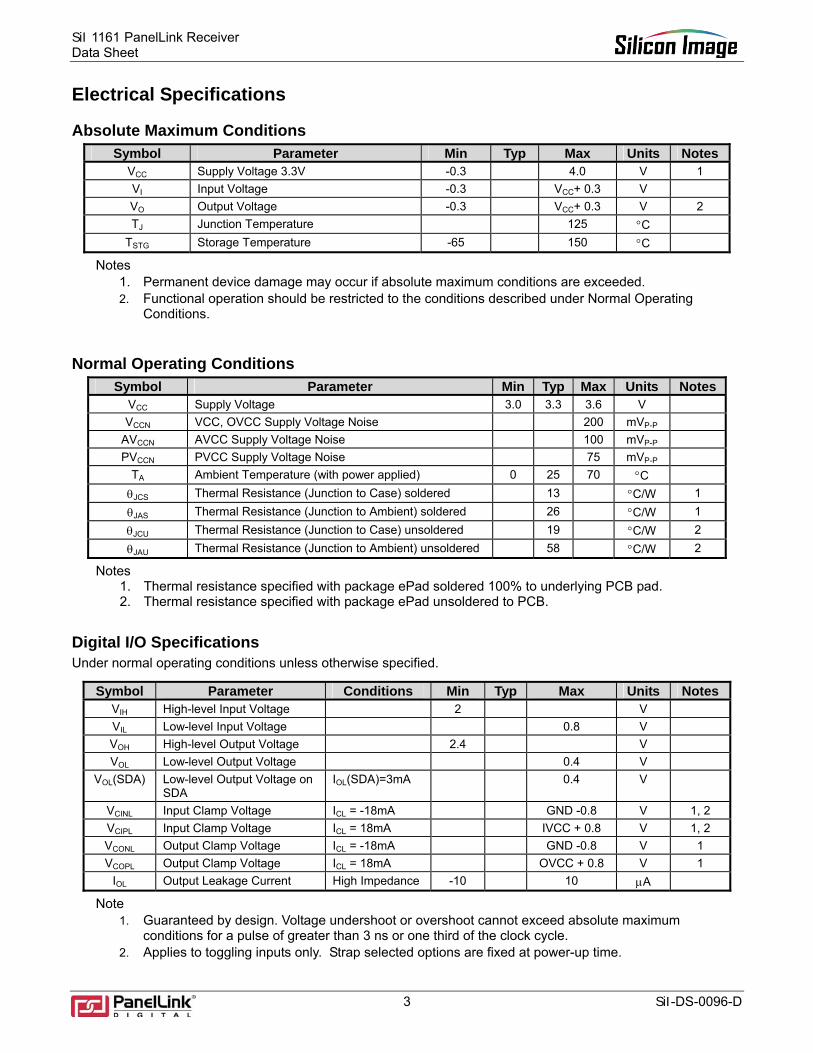
Absolute Maximum Conditions Symbol Parameter Min Typ Max Units Notes
VCC Supply Voltage 3.3V -0.3 4.0 V 1 VI Input Voltage -0.3 VCC+ 0.3 V VO Output Voltage -0.3 VCC+ 0.3 V 2 TJ Junction Temperature 125 °C
TSTG Storage Temperature -65 150 °C
Notes 1. Permanent device damage may occur if absolute maximum conditions are exceeded. 2. Functional operation should be restricted to the conditions described under Normal Operating
Conditions.
Normal Operating Conditions Symbol Parameter Min Typ Max Units Notes
VCC Supply Voltage 3.0 3.3 3.6 V VCCN VCC, OVCC Supply Voltage Noise 200 mVP-P
AVCCN AVCC Supply Voltage Noise 100 mVP-P PVCCN PVCC Supply Voltage Noise 75 mVP-P
TA Ambient Temperature (with power applied) 0 25 70 °C θJCS Thermal Resistance (Junction to Case) soldered 13 °C/W 1 θJAS Thermal Resistance (Junction to Ambient) soldered 26 °C/W 1 θJCU Thermal Resistance (Junction to Case) unsoldered 19 °C/W 2 θJAU Thermal Resistance (Junction to Ambient) unsoldered 58 °C/W 2
Notes 1. Thermal resistance specified with package ePad soldered 100% to underlying PCB pad. 2. Thermal resistance specified with package ePad unsoldered to PCB.
Digital I/O Specifications Under normal operating conditions unless otherwise specified.
Symbol Parameter Conditions Min Typ Max Units Notes VIH High-level Input Voltage 2 V VIL Low-level Input Voltage 0.8 V VOH High-level Output Voltage 2.4 V VOL Low-level Output Voltage 0.4 V
VOL(SDA) Low-level Output Voltage on SDA
IOL(SDA)=3mA 0.4 V
VCINL Input Clamp Voltage ICL = -18mA GND -0.8 V 1, 2 VCIPL Input Clamp Voltage ICL = 18mA IVCC + 0.8 V 1, 2 VCONL Output Clamp Voltage ICL = -18mA GND -0.8 V 1 VCOPL Output Clamp Voltage ICL = 18mA OVCC + 0.8 V 1
IOL Output Leakage Current High Impedance -10 10 µA
Note 1. Guaranteed by design. Voltage undershoot or overshoot cannot exceed absolute maximum
conditions for a pulse of greater than 3 ns or one third of the clock cycle. 2. Applies to toggling inputs only. Strap selected options are fixed at power-up time.
SiI 1161 PanelLink ReceiverData Sheet
SiI-DS-0096-D 4
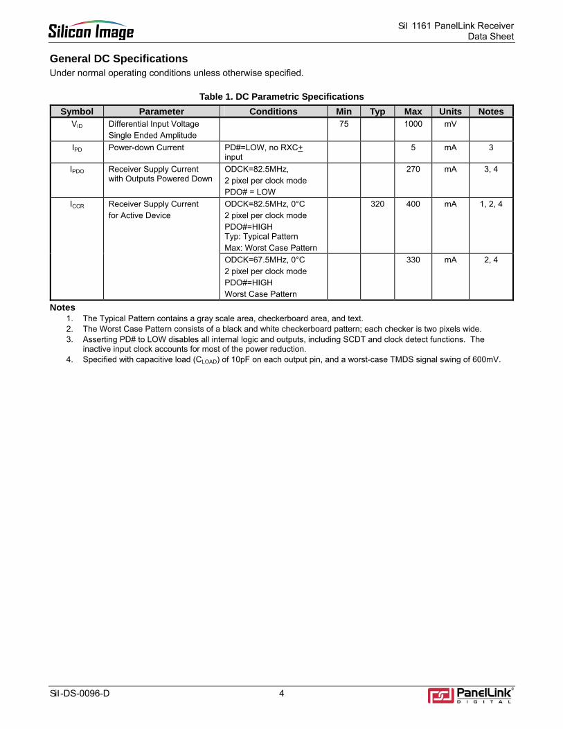
General DC Specifications Under normal operating conditions unless otherwise specified.
Table 1. DC Parametric Specifications Symbol Parameter Conditions Min Typ Max Units Notes
VID Differential Input Voltage Single Ended Amplitude
75 1000 mV
IPD Power-down Current PD#=LOW, no RXC+ input
5 mA 3
IPDO Receiver Supply Current with Outputs Powered Down
ODCK=82.5MHz, 2 pixel per clock mode PDO# = LOW
270 mA 3, 4
ICCR Receiver Supply Current for Active Device
ODCK=82.5MHz, 0°C 2 pixel per clock mode PDO#=HIGH Typ: Typical Pattern Max: Worst Case Pattern
320
400 mA 1, 2, 4
ODCK=67.5MHz, 0°C 2 pixel per clock mode PDO#=HIGH Worst Case Pattern
330 mA 2, 4
Notes 1. The Typical Pattern contains a gray scale area, checkerboard area, and text. 2. The Worst Case Pattern consists of a black and white checkerboard pattern; each checker is two pixels wide. 3. Asserting PD# to LOW disables all internal logic and outputs, including SCDT and clock detect functions. The
inactive input clock accounts for most of the power reduction. 4. Specified with capacitive load (CLOAD) of 10pF on each output pin, and a worst-case TMDS signal swing of 600mV.
SiI 1161 PanelLink Receiver Data Sheet
5 SiI-DS-0096-D
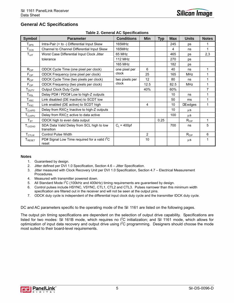
General AC Specifications
Table 2. General AC Specifications Symbol Parameter Conditions Min Typ Max Units Notes
TDPS Intra-Pair (+ to -) Differential Input Skew 165MHz 245 ps 1 TCCS Channel to Channel Differential Input Skew 165MHz 4 ns 1 TIJIT Worst Case Differential Input Clock Jitter 65 MHz 465 ps 2,3
tolerance 112 MHz 270 ps 165 MHz 182 ps
RCIP ODCK Cycle Time (one pixel per clock) 6 40 ns 1 FCIP ODCK Frequency (one pixel per clock)
one pixel per clock 25 165 MHz 1
RCIP ODCK Cycle Time (two pixels per clock) 12 80 ns 1 FCIP ODCK Frequency (two pixels per clock)
two pixels per clock 12.5 82.5 MHz 1
TDUTY Output Clock Duty Cycle 40% 60% 7 TPDL Delay PD# / PDO# Low to high-Z outputs 10 ns 1 THSC Link disabled (DE inactive) to SCDT low 50 ms 1 TFSC Link enabled (DE active) to SCDT high 4 10 DE edges 1
TCLKPD Delay from RXC+ Inactive to high-Z outputs 10 µs TCLKPU Delay from RXC+ active to data active 100 µs
TST ODCK high to even data output 0.25 RCIP 1 TI2CDVD SDA Data Valid Delay from SCL high to low
transition CL = 400pf 700 ns 5
TCTLW Control Pulse Width 2 RCIP 6 TRESET PD# Signal Low Time required for a valid I2C
reset 10 µs 1
Notes 1. Guaranteed by design. 2. Jitter defined per DVI 1.0 Specification, Section 4.6 – Jitter Specification. 3. Jitter measured with Clock Recovery Unit per DVI 1.0 Specification, Section 4.7 – Electrical Measurement
Procedures. 4. Measured with transmitter powered down. 5. All Standard Mode I2C (100kHz and 400kHz) timing requirements are guaranteed by design. 6. Control pulses include HSYNC, VSYNC, CTL1, CTL2 and CTL3. Pulses narrower than this minimum width
specification are filtered out in the receiver and will not be seen at the output pins. 7. ODCK duty cycle is independent of the differential input clock duty cycle and the transmitter IDCK duty cycle.
DC and AC parameters specific to the operating mode of the SiI 1161 are listed on the following pages.
The output pin timing specifications are dependent on the selection of output drive capability. Specifications are listed for two modes: SiI 161B mode, which requires no I2C initialization; and SiI 1161 mode, which allows for optimization of input data recovery and output drive using I2C programming. Designers should choose the mode most suited to their board-level requirements.
SiI 1161 PanelLink ReceiverData Sheet
SiI-DS-0096-D 6
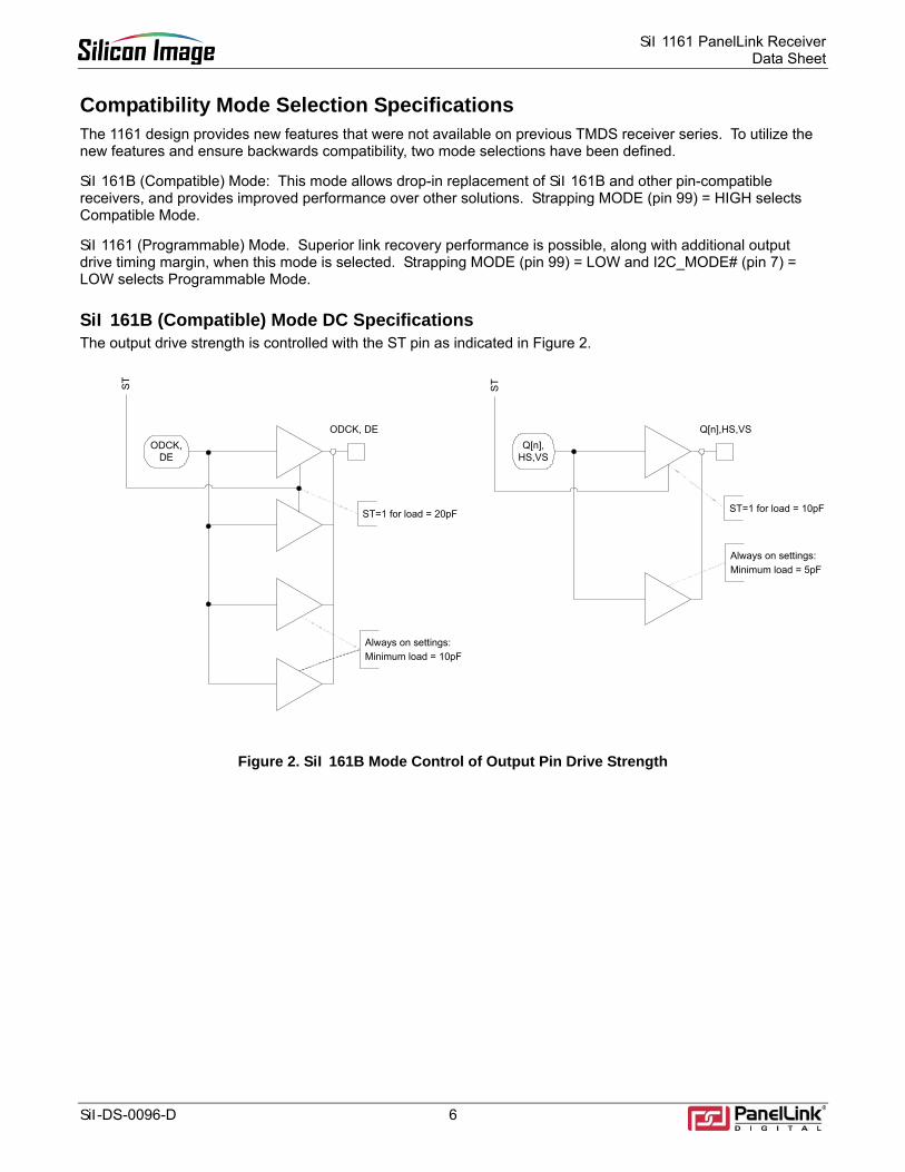
Compatibility Mode Selection Specifications The 1161 design provides new features that were not available on previous TMDS receiver series. To utilize the new features and ensure backwards compatibility, two mode selections have been defined.
SiI 161B (Compatible) Mode: This mode allows drop-in replacement of SiI 161B and other pin-compatible receivers, and provides improved performance over other solutions. Strapping MODE (pin 99) = HIGH selects Compatible Mode.
SiI 1161 (Programmable) Mode. Superior link recovery performance is possible, along with additional output drive timing margin, when this mode is selected. Strapping MODE (pin 99) = LOW and I2C_MODE# (pin 7) = LOW selects Programmable Mode.
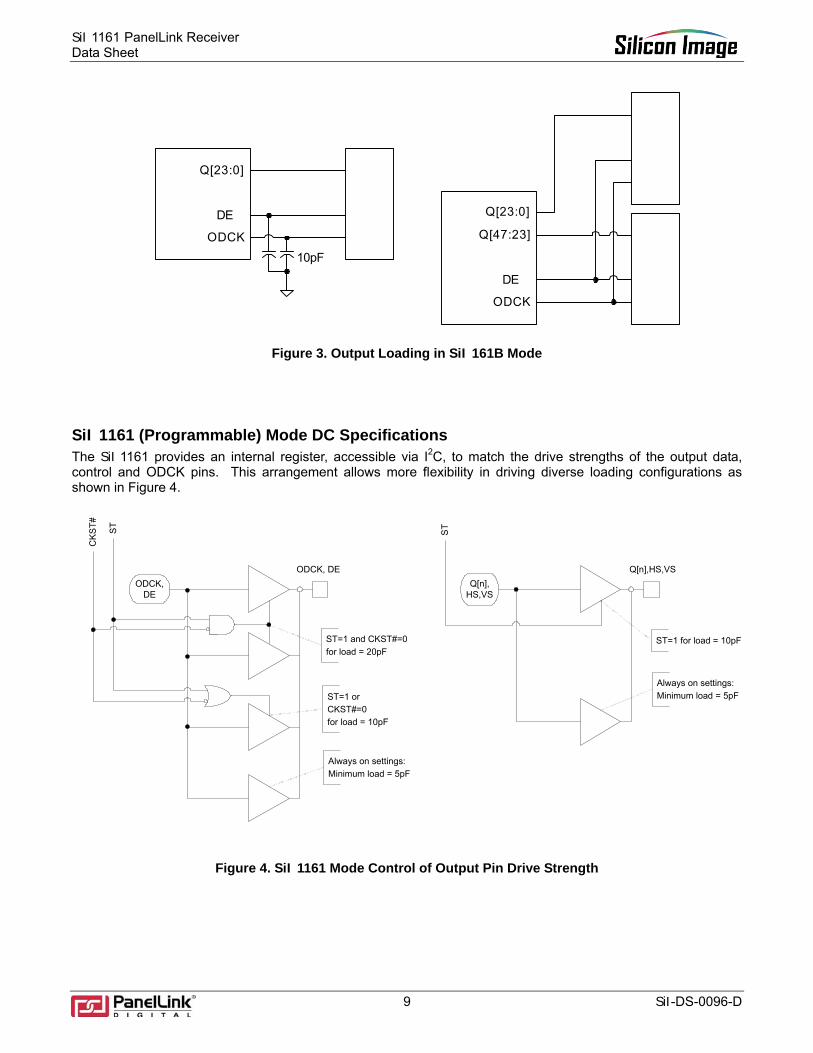
SiI 161B (Compatible) Mode DC Specifications The output drive strength is controlled with the ST pin as indicated in Figure 2.
Figure 2. SiI 161B Mode Control of Output Pin Drive Strength
ODCK, DE
ST
ODCK,DE
Always on settings:Minimum load = 10pF
ST=1 for load = 20pF
Q[n],HS,VS
ST
Q[n],HS,VS
Always on settings:Minimum load = 5pF
ST=1 for load = 10pF
SiI 1161 PanelLink Receiver Data Sheet
7 SiI-DS-0096-D
The output drive specifications in the Compatible mode are equivalent to the drive on the SiI 161B part.
Table 3. SiI 161B Mode DC Specifications
Strap option: ST=0 (Low Drive Strength)
Parameter Conditions Limits (mA) Notes ST VOUT CL Min Typ Max
Data and Controls IOHD Output High Drive 0 2.4V 5pF 3.8 1 IOLD Output Low Drive 0 0.8V 5pF 5.5 2
0 0.4V 5pF 3.2 3 ODCK and DE
IOHC Output High Drive 0 2.4V 10pF 7.5 4 IOLC Output Low Drive 0 0.8V 10pF 11.1
0 0.4V 10pF 6.2
Strap option: ST=1 (High Drive Strength)
Parameter Conditions Limits (mA) Notes ST VOUT CL Min Typ Max
Data and Controls IOHD Output High Drive 1 2.4V 10pF 7.4 1 IOLD Output Low Drive 1 0.8V 10pF 11.1 2
1 0.4V 10pF 6.3 3 ODCK and DE
IOHC Output High Drive 1 2.4V 20pF 14.7 4 IOLC Output Low Drive 1 0.8V 20pF 21.2
1 0.4V 20pF 12.3 Notes
1. Output loading is equivalent to one or two CMOS input loads. 2. 0.8V corresponds to LVTTL VIN(max). 3. 0.4V corresponds to LVCMOS VIN(max). 4. Output loading is equivalent to two or four CMOS input loads.
SiI 1161 PanelLink ReceiverData Sheet
SiI-DS-0096-D 8
SiI 161B (Compatible) Mode AC Specifications AC timings are provided here in setup/hold format at 165MHz for ease of direct comparison to the SiI 161B part. Timing specifications in Table 4 apply to worst-case one pixel per clock mode. For other modes and frequencies use the SiI 1161 Mode timings and calculation methodology, “Calculating Setup and Hold Times” on Page 12.
Table 4. SiI 161B Mode AC Specifications Strap option: ST=0 (Low Drive Strength)
Parameter Conditions Limits (ns) Data, HSYNC, VSYNC Max
DHLT 1-to-0 Transition CL=5pF 2.5 DLHT 0-to-1 Transition CL=5pF 2.0
ODCK, DE Max DHLT 1-to-0 Transition CL=5pF 1.5 DLHT 0-to-1 Transition CL=5pF 1.7
Timing @ 165MHz Min OCK_INV=0
Min OCK_INV=1
TSETUP Data CL=5pF 0.9 1.2 DE, HSYNC, VSYNC CL=5pF 0.2 0.4
THOLD Data CL=5pF 2.8 2.4 DE, HSYNC, VSYNC CL=5pF 3.6 2.6
Strap option: ST=1 (High Drive Strength)
Parameter Conditions Limits (ns) Data, HSYNC, VSYNC Max
DHLT 1-to-0 Transition CL=10pF 2.5 DLHT 0-to-1 Transition CL=10pF 2.0
ODCK, DE Max DHLT 1-to-0 Transition CL=10pF 1.2 DLHT 0-to-1 Transition CL=10pF 1.4
Timing @ 165MHz Min OCK_INV=0
Min OCK_INV=1
TSETUP Data CL=10pF 0.9 1.2 DE, HSYNC, VSYNC CL=10pF 0.6 1.1
THOLD Data CL=10pF 2.8 2.2 DE, HSYNC, VSYNC CL=10pF 3.1 2.1
Notes 1. All transitions are specified at worst case of 70ºC with minimum VCC. 2. ODCK and DE output pins should be loaded with 10pF when ST=0 and 20pF when ST=1. If layout requires only a
point-to-point, one load net, a discrete 10pF capacitor should be added to the net to create these loads. See Figure 3.
SiI 1161 PanelLink Receiver Data Sheet
9 SiI-DS-0096-D
ODCK
DE
Q[23:0]
ODCK
DE
Q[47:23]
Q[23:0]
10pF
Figure 3. Output Loading in SiI 161B Mode
SiI 1161 (Programmable) Mode DC Specifications The SiI 1161 provides an internal register, accessible via I2C, to match the drive strengths of the output data, control and ODCK pins. This arrangement allows more flexibility in driving diverse loading configurations as shown in Figure 4.
Figure 4. SiI 1161 Mode Control of Output Pin Drive Strength
ODCK, DE
ST
CKS
T#
ODCK,DE
Always on settings:Minimum load = 5pF
ST=1 and CKST#=0for load = 20pF
ST=1 orCKST#=0for load = 10pF
Q[n],HS,VS
ST
Q[n],HS,VS
Always on settings:Minimum load = 5pF
ST=1 for load = 10pF
SiI 1161 PanelLink ReceiverData Sheet
SiI-DS-0096-D 10
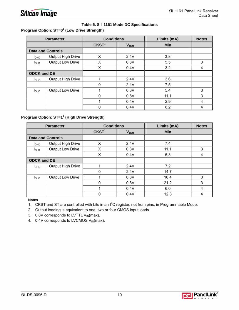
Table 5. SiI 1161 Mode DC Specifications Program Option: ST=01 (Low Drive Strength)
Parameter Conditions Limits (mA) Notes CKST1 VOUT Min
Data and Controls IOHD Output High Drive X 2.4V 3.8 IOLD Output Low Drive X 0.8V 5.5 3
X 0.4V 3.2 4 ODCK and DE
IOHC Output High Drive 1 2.4V 3.6 0 2.4V 7.5
IOLC Output Low Drive 1 0.8V 5.4 3 0 0.8V 11.1 3 1 0.4V 2.9 4 0 0.4V 6.2 4
Program Option: ST=11 (High Drive Strength)
Parameter Conditions Limits (mA) Notes CKST1 VOUT Min
Data and Controls IOHD Output High Drive X 2.4V 7.4 IOLD Output Low Drive X 0.8V 11.1 3
X 0.4V 6.3 4 ODCK and DE
IOHC Output High Drive 1 2.4V 7.2 0 2.4V 14.7
IOLC Output Low Drive 1 0.8V 10.4 3 0 0.8V 21.2 3 1 0.4V 6.0 4 0 0.4V 12.3 4 Notes 1. CKST and ST are controlled with bits in an I2C register, not from pins, in Programmable Mode. 2. Output loading is equivalent to one, two or four CMOS input loads. 3. 0.8V corresponds to LVTTL VIN(max). 4. 0.4V corresponds to LVCMOS VIN(max).
SiI 1161 PanelLink Receiver Data Sheet
11 SiI-DS-0096-D
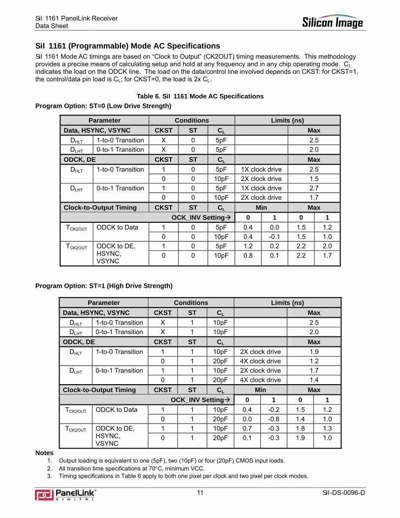
SiI 1161 (Programmable) Mode AC Specifications SiI 1161 Mode AC timings are based on “Clock to Output” (CK2OUT) timing measurements. This methodology provides a precise means of calculating setup and hold at any frequency and in any chip operating mode. CL indicates the load on the ODCK line. The load on the data/control line involved depends on CKST: for CKST=1, the control/data pin load is CL; for CKST=0, the load is 2x CL.
Table 6. SiI 1161 Mode AC Specifications Program Option: ST=0 (Low Drive Strength)
Parameter Conditions Limits (ns) Data, HSYNC, VSYNC CKST ST CL Max
DHLT 1-to-0 Transition X 0 5pF 2.5 DLHT 0-to-1 Transition X 0 5pF 2.0
ODCK, DE CKST ST CL Max DHLT 1-to-0 Transition 1 0 5pF 1X clock drive 2.5
0 0 10pF 2X clock drive 1.5 DLHT 0-to-1 Transition 1 0 5pF 1X clock drive 2.7
0 0 10pF 2X clock drive 1.7 Clock-to-Output Timing CKST ST CL Min Max
OCK_INV Setting 0 1 0 1 TCK2OUT 1 0 5pF 0.4 0.0 1.5 1.2
ODCK to Data
0 0 10pF 0.4 -0.1 1.5 1.0 TCK2OUT 1 0 5pF 1.2 0.2 2.2 2.0
ODCK to DE, HSYNC, VSYNC
0 0 10pF 0.8 0.1 2.2 1.7
Program Option: ST=1 (High Drive Strength)
Parameter Conditions Limits (ns) Data, HSYNC, VSYNC CKST ST CL Max
DHLT 1-to-0 Transition X 1 10pF 2.5 DLHT 0-to-1 Transition X 1 10pF 2.0
ODCK, DE CKST ST CL Max DHLT 1-to-0 Transition 1 1 10pF 2X clock drive 1.9
0 1 20pF 4X clock drive 1.2 DLHT 0-to-1 Transition 1 1 10pF 2X clock drive 1.7
0 1 20pF 4X clock drive 1.4 Clock-to-Output Timing CKST ST CL Min Max
OCK_INV Setting 0 1 0 1 TCK2OUT 1 1 10pF 0.4 -0.2 1.5 1.2
ODCK to Data
0 1 20pF 0.0 -0.8 1.4 1.0 TCK2OUT 1 1 10pF 0.7 -0.3 1.8 1.3
ODCK to DE, HSYNC, VSYNC
0 1 20pF 0.1 -0.3 1.9 1.0
Notes 1. Output loading is equivalent to one (5pF), two (10pF) or four (20pF) CMOS input loads. 2. All transition time specifications at 70°C, minimum VCC. 3. Timing specifications in Table 6 apply to both one pixel per clock and two pixel per clock modes.
SiI 1161 PanelLink ReceiverData Sheet
SiI-DS-0096-D 12
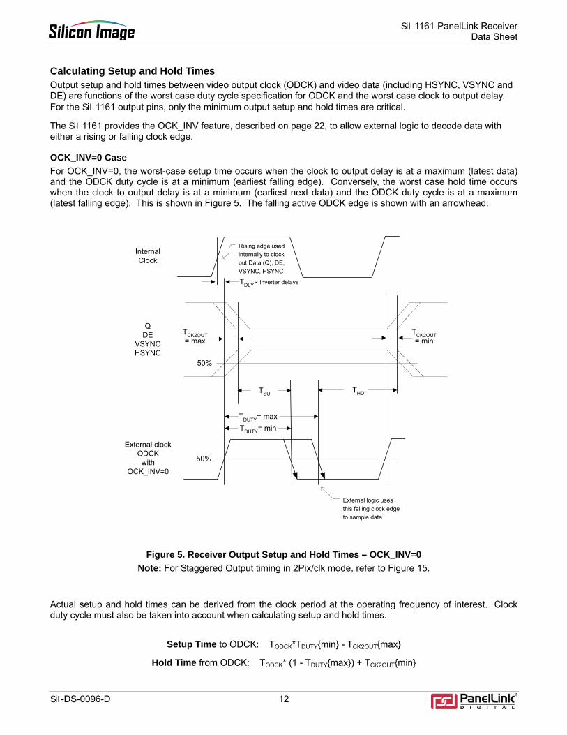
Calculating Setup and Hold Times Output setup and hold times between video output clock (ODCK) and video data (including HSYNC, VSYNC and DE) are functions of the worst case duty cycle specification for ODCK and the worst case clock to output delay. For the SiI 1161 output pins, only the minimum output setup and hold times are critical.
The SiI 1161 provides the OCK_INV feature, described on page 22, to allow external logic to decode data with either a rising or falling clock edge.
OCK_INV=0 Case For OCK_INV=0, the worst-case setup time occurs when the clock to output delay is at a maximum (latest data) and the ODCK duty cycle is at a minimum (earliest falling edge). Conversely, the worst case hold time occurs when the clock to output delay is at a minimum (earliest next data) and the ODCK duty cycle is at a maximum (latest falling edge). This is shown in Figure 5. The falling active ODCK edge is shown with an arrowhead.
Figure 5. Receiver Output Setup and Hold Times – OCK_INV=0 Note: For Staggered Output timing in 2Pix/clk mode, refer to Figure 15.
Actual setup and hold times can be derived from the clock period at the operating frequency of interest. Clock duty cycle must also be taken into account when calculating setup and hold times.
Setup Time to ODCK: TODCK*TDUTYmin - TCK2OUTmax
Hold Time from ODCK: TODCK* (1 - TDUTYmax) + TCK2OUTmin
TDUTY= min
TCK2OUT= max
External clockODCK
withOCK_INV=0
QDE
VSYNCHSYNC
50%
THDTSU
TCK2OUT= min
TDUTY= max
50%
Rising edge usedinternally to clockout Data (Q), DE,VSYNC, HSYNC
External logic usesthis falling clock edgeto sample data
InternalClock
TDLY - inverter delays
SiI 1161 PanelLink Receiver Data Sheet
13 SiI-DS-0096-D
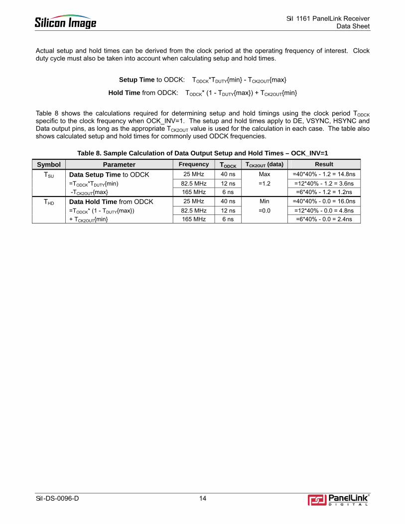
Table 7 shows the calculations required for determining setup and hold timings using the clock period TODCK specific to the clock frequency, also bringing in the clock duty cycle as required when OCK_INV=0. The setup and hold times apply to DE, VSYNC, HSYNC and Data output pins, as long as the appropriate TCK2OUT value is used for the calculation in each case. The table also shows calculated setup and hold times for commonly used ODCK frequencies.
Table 7. Sample Calculation of Data Output Setup and Hold Times – OCK_INV=0 Symbol Parameter Frequency TODCK TCK2OUT (data) Result
Data Setup Time to ODCK 25 MHz 40 ns Max =40*40% - 1.5 = 14.5ns =TODCK*TDUTYmin) 82.5 MHz 12 ns =1.5 =12*40% - 1.5 = 3.3ns
TSU
-TCK2OUTmax 165 MHz 6 ns =6*40% - 1.5 = 0.9ns
Data Hold Time from ODCK 25 MHz 40 ns Min =40*40% + 0.4 = 16.4ns =TODCK* (1 - TDUTYmax) 82.5 MHz 12 ns =0.4 =12*40% + 0.4 = 5.2ns
THD
+ TCK2OUTmin 165 MHz 6 ns =6*40% + 0.4 = 2.8ns
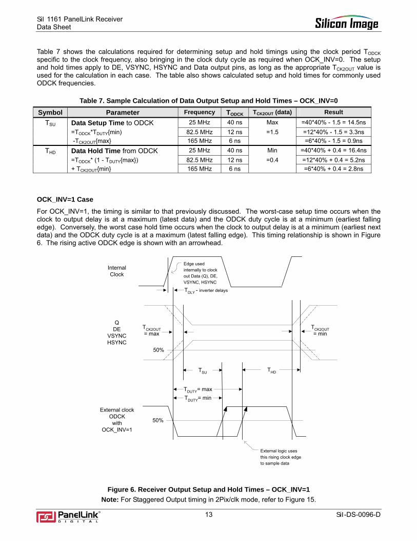
OCK_INV=1 Case
For OCK_INV=1, the timing is similar to that previously discussed. The worst-case setup time occurs when the clock to output delay is at a maximum (latest data) and the ODCK duty cycle is at a minimum (earliest falling edge). Conversely, the worst case hold time occurs when the clock to output delay is at a minimum (earliest next data) and the ODCK duty cycle is at a maximum (latest falling edge). This timing relationship is shown in Figure 6. The rising active ODCK edge is shown with an arrowhead.
Figure 6. Receiver Output Setup and Hold Times – OCK_INV=1 Note: For Staggered Output timing in 2Pix/clk mode, refer to Figure 15.
TDUTY= min
TCK2OUT= max
External clockODCK
withOCK_INV=1
QDE
VSYNCHSYNC
50%
THDTSU
TCK2OUT= min
TDUTY= max
50%
Edge usedinternally to clockout Data (Q), DE,VSYNC, HSYNC
External logic usesthis rising clock edgeto sample data
InternalClock
TDLY - inverter delays
SiI 1161 PanelLink ReceiverData Sheet
SiI-DS-0096-D 14
Actual setup and hold times can be derived from the clock period at the operating frequency of interest. Clock duty cycle must also be taken into account when calculating setup and hold times.
Setup Time to ODCK: TODCK*TDUTYmin - TCK2OUTmax
Hold Time from ODCK: TODCK* (1 - TDUTYmax) + TCK2OUTmin
Table 8 shows the calculations required for determining setup and hold timings using the clock period TODCK specific to the clock frequency when OCK_INV=1. The setup and hold times apply to DE, VSYNC, HSYNC and Data output pins, as long as the appropriate TCK2OUT value is used for the calculation in each case. The table also shows calculated setup and hold times for commonly used ODCK frequencies.
Table 8. Sample Calculation of Data Output Setup and Hold Times – OCK_INV=1 Symbol Parameter Frequency TODCK TCK2OUT (data) Result
Data Setup Time to ODCK 25 MHz 40 ns Max =40*40% - 1.2 = 14.8ns =TODCK*TDUTYmin) 82.5 MHz 12 ns =1.2 =12*40% - 1.2 = 3.6ns
TSU
-TCK2OUTmax 165 MHz 6 ns =6*40% - 1.2 = 1.2ns
Data Hold Time from ODCK 25 MHz 40 ns Min =40*40% - 0.0 = 16.0ns =TODCK* (1 - TDUTYmax) 82.5 MHz 12 ns =0.0 =12*40% - 0.0 = 4.8ns
THD
+ TCK2OUTmin 165 MHz 6 ns =6*40% - 0.0 = 2.4ns
SiI 1161 PanelLink Receiver Data Sheet
15 SiI-DS-0096-D
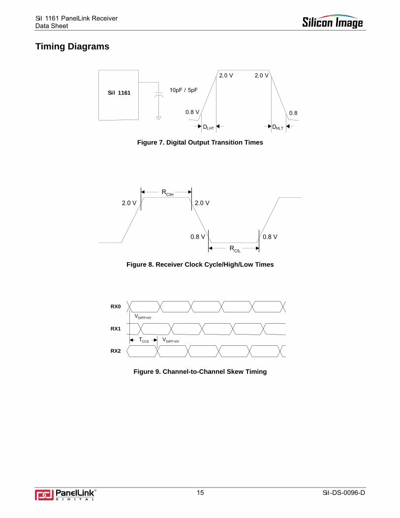
Timing Diagrams
10pF / 5pFSiI 1161
DHLT
2.0 V 2.0 V
0.8 V 0.8
DLHT
Figure 7. Digital Output Transition Times
RCIH
RCIL
2.0 V
0.8 V0.8 V
2.0 V
Figure 8. Receiver Clock Cycle/High/Low Times
RX0
RX1
RX2
T CCS
V DIFF=0V
VDIFF=0V
Figure 9. Channel-to-Channel Skew Timing
SiI 1161 PanelLink ReceiverData Sheet
SiI-DS-0096-D 16
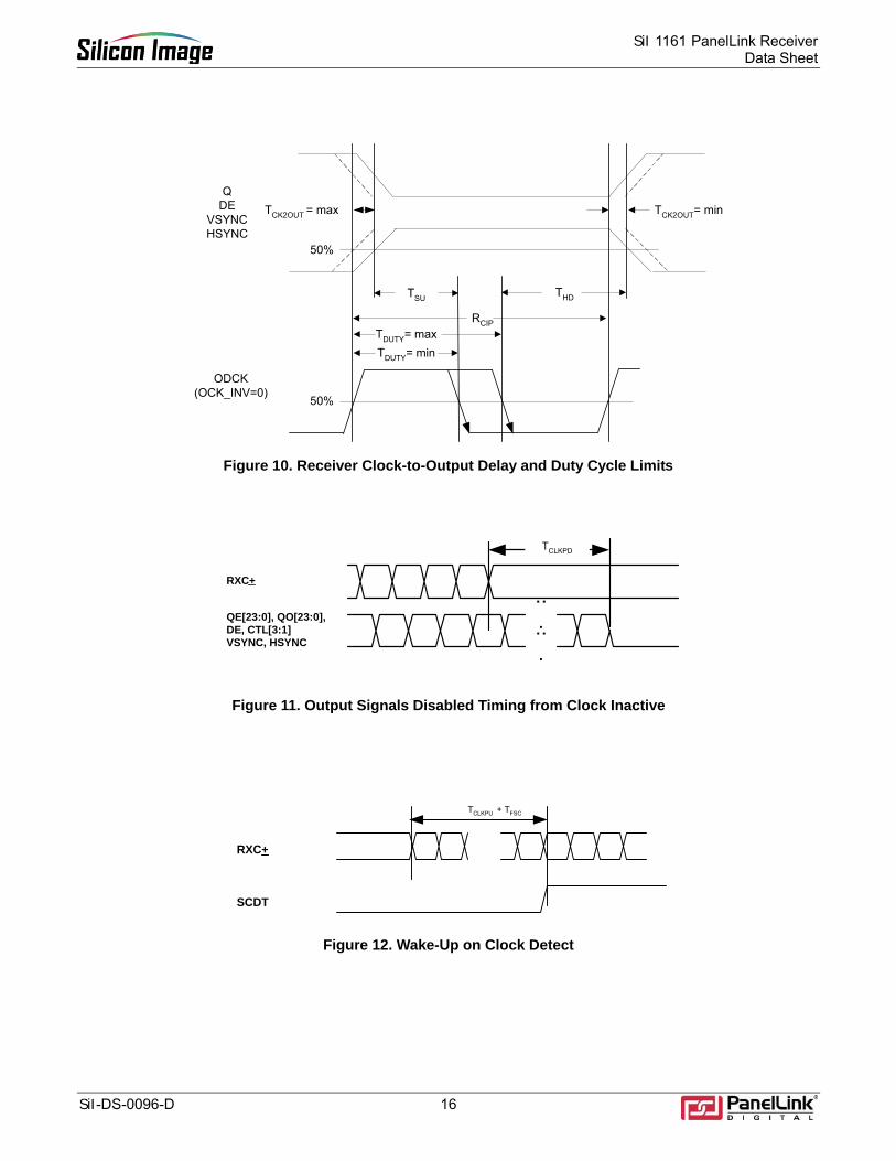
RXC+
QE[23:0], QO[23:0],DE, CTL[3:1]VSYNC, HSYNC
TCLKPD
......
Figure 10. Receiver Clock-to-Output Delay and Duty Cycle Limits
Figure 11. Output Signals Disabled Timing from Clock Inactive
Figure 12. Wake-Up on Clock Detect
RXC+
SCDT
TCLKPU + TFSC
TDUTY= min
TCK2OUT = max
ODCK(OCK_INV=0)
QDE
VSYNCHSYNC
50%
THDTSU
TCK2OUT= min
TDUTY= max
50%
RCIP
SiI 1161 PanelLink Receiver Data Sheet
17 SiI-DS-0096-D
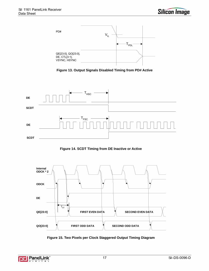
TPDL
QE[23:0], QO[23:0],DE, CTL[3:1],VSYNC, HSYNC
PD#VIL
Figure 13. Output Signals Disabled Timing from PD# Active
Figure 14. SCDT Timing from DE Inactive or Active
ODCK
DE
QE[23:0]
QO[23:0]
FIRST EVEN DATA SECOND EVEN DATA
Internal ODCK * 2
FIRST ODD DATA SECOND ODD DATA
T ST
Figure 15. Two Pixels per Clock Staggered Output Timing Diagram
DE
SCDT
DE
SCDT
THSC
T FSC
SiI 1161 PanelLink ReceiverData Sheet
SiI-DS-0096-D 18
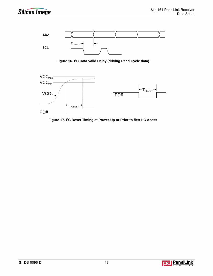
SCL
SDA
TI2CDVD
Figure 16. I2C Data Valid Delay (driving Read Cycle data)
VCC max
T RESET
VCC min
VCC
PD#
TRESET PD#
Figure 17. I2C Reset Timing at Power-Up or Prior to first I2C Acess
SiI 1161 PanelLink Receiver Data Sheet
19 SiI-DS-0096-D
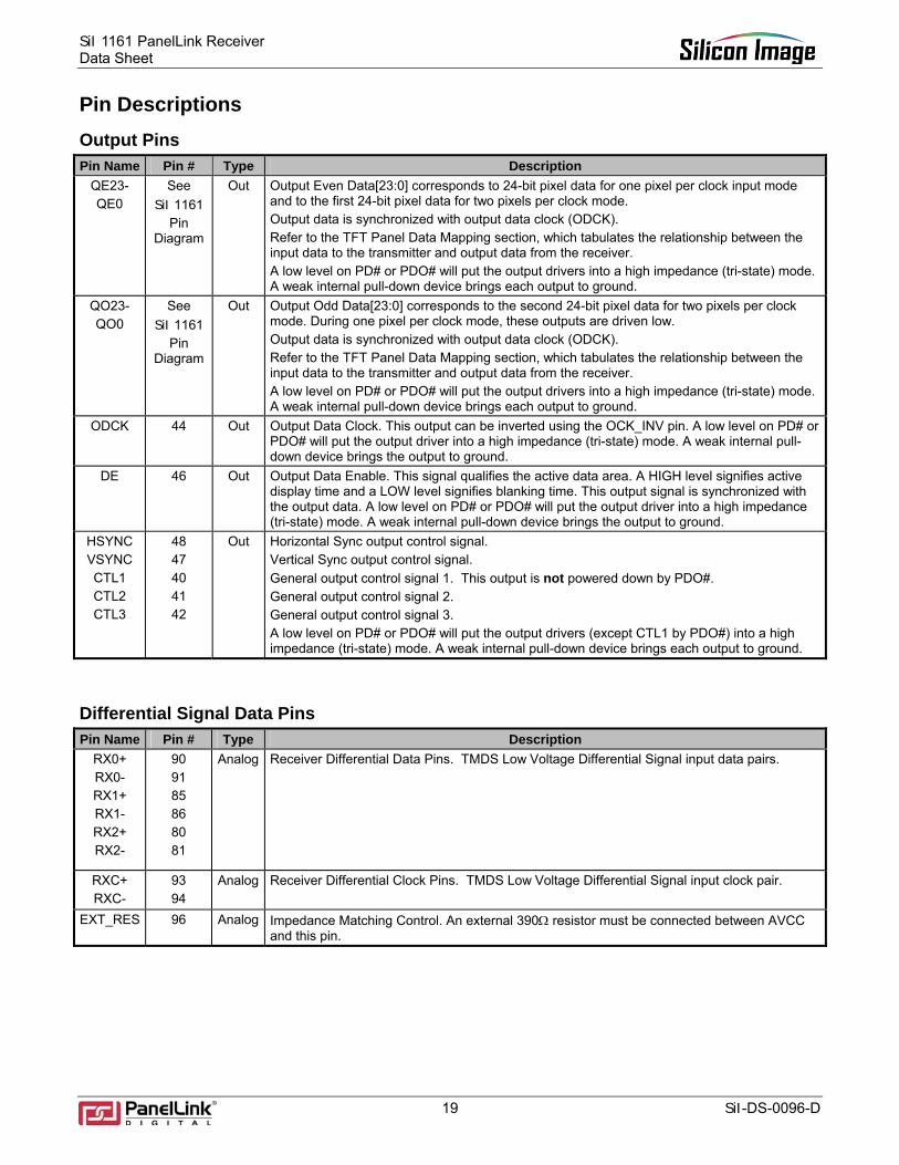
Pin Descriptions Output Pins Pin Name Pin # Type Description
QE23- QE0
See SiI 1161
Pin Diagram
Out Output Even Data[23:0] corresponds to 24-bit pixel data for one pixel per clock input mode and to the first 24-bit pixel data for two pixels per clock mode. Output data is synchronized with output data clock (ODCK). Refer to the TFT Panel Data Mapping section, which tabulates the relationship between the input data to the transmitter and output data from the receiver. A low level on PD# or PDO# will put the output drivers into a high impedance (tri-state) mode. A weak internal pull-down device brings each output to ground.
QO23- QO0
See SiI 1161
Pin Diagram
Out Output Odd Data[23:0] corresponds to the second 24-bit pixel data for two pixels per clock mode. During one pixel per clock mode, these outputs are driven low. Output data is synchronized with output data clock (ODCK). Refer to the TFT Panel Data Mapping section, which tabulates the relationship between the input data to the transmitter and output data from the receiver. A low level on PD# or PDO# will put the output drivers into a high impedance (tri-state) mode. A weak internal pull-down device brings each output to ground.
ODCK 44 Out Output Data Clock. This output can be inverted using the OCK_INV pin. A low level on PD# or PDO# will put the output driver into a high impedance (tri-state) mode. A weak internal pull-down device brings the output to ground.
DE 46 Out Output Data Enable. This signal qualifies the active data area. A HIGH level signifies active display time and a LOW level signifies blanking time. This output signal is synchronized with the output data. A low level on PD# or PDO# will put the output driver into a high impedance (tri-state) mode. A weak internal pull-down device brings the output to ground.
HSYNC VSYNC CTL1 CTL2 CTL3
48 47 40 41 42
Out
Horizontal Sync output control signal. Vertical Sync output control signal. General output control signal 1. This output is not powered down by PDO#. General output control signal 2. General output control signal 3. A low level on PD# or PDO# will put the output drivers (except CTL1 by PDO#) into a high impedance (tri-state) mode. A weak internal pull-down device brings each output to ground.
Differential Signal Data Pins Pin Name Pin # Type Description
RX0+ RX0- RX1+ RX1- RX2+ RX2-
90 91 85 86 80 81
Analog
Receiver Differential Data Pins. TMDS Low Voltage Differential Signal input data pairs.
RXC+ RXC-
93 94
Analog
Receiver Differential Clock Pins. TMDS Low Voltage Differential Signal input clock pair.
EXT_RES 96 Analog Impedance Matching Control. An external 390Ω resistor must be connected between AVCC and this pin.
SiI 1161 PanelLink ReceiverData Sheet
SiI-DS-0096-D 20
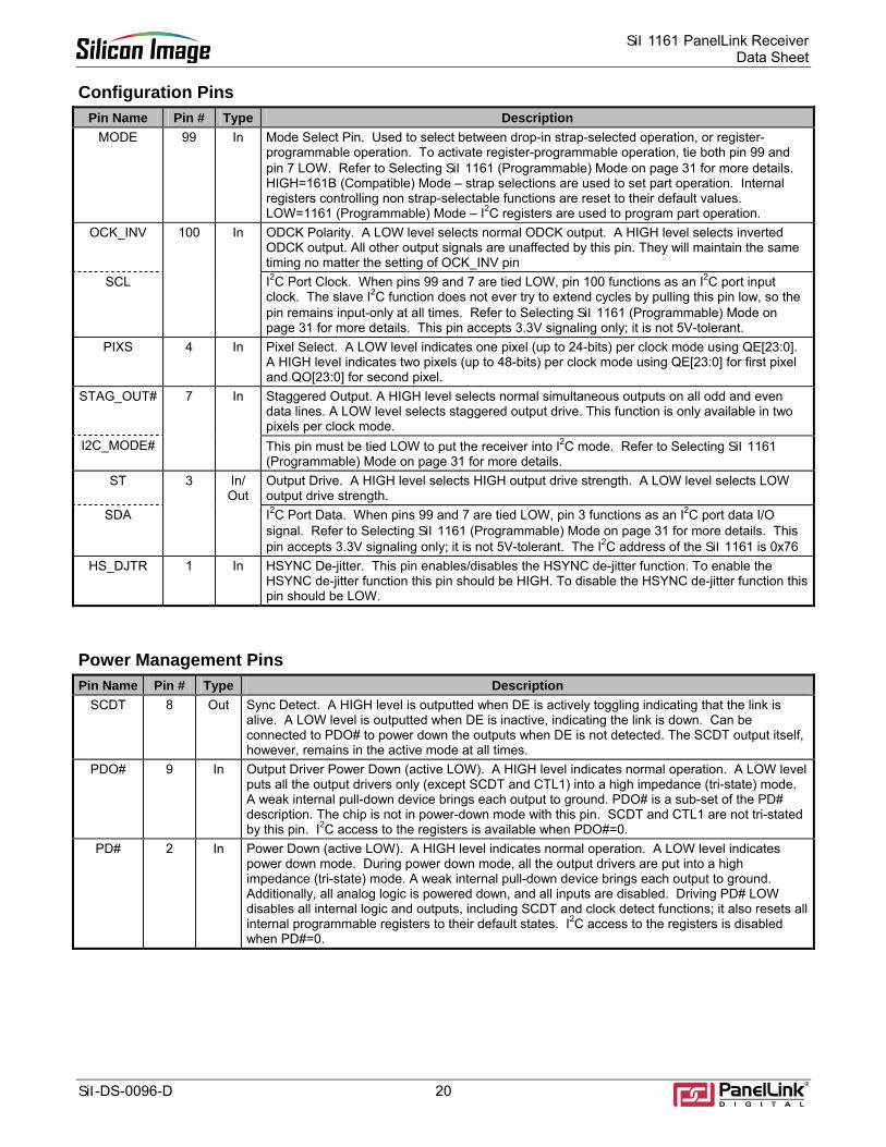
Configuration Pins Pin Name Pin # Type Description
MODE 99 In Mode Select Pin. Used to select between drop-in strap-selected operation, or register-programmable operation. To activate register-programmable operation, tie both pin 99 and pin 7 LOW. Refer to Selecting SiI 1161 (Programmable) Mode on page 31 for more details. HIGH=161B (Compatible) Mode – strap selections are used to set part operation. Internal registers controlling non strap-selectable functions are reset to their default values. LOW=1161 (Programmable) Mode – I2C registers are used to program part operation.
OCK_INV 100 In
ODCK Polarity. A LOW level selects normal ODCK output. A HIGH level selects inverted ODCK output. All other output signals are unaffected by this pin. They will maintain the same timing no matter the setting of OCK_INV pin
SCL I2C Port Clock. When pins 99 and 7 are tied LOW, pin 100 functions as an I2C port input clock. The slave I2C function does not ever try to extend cycles by pulling this pin low, so the pin remains input-only at all times. Refer to Selecting SiI 1161 (Programmable) Mode on page 31 for more details. This pin accepts 3.3V signaling only; it is not 5V-tolerant.
PIXS 4 In Pixel Select. A LOW level indicates one pixel (up to 24-bits) per clock mode using QE[23:0]. A HIGH level indicates two pixels (up to 48-bits) per clock mode using QE[23:0] for first pixel and QO[23:0] for second pixel.
STAG_OUT# 7 In Staggered Output. A HIGH level selects normal simultaneous outputs on all odd and even data lines. A LOW level selects staggered output drive. This function is only available in two pixels per clock mode.
I2C_MODE# This pin must be tied LOW to put the receiver into I2C mode. Refer to Selecting SiI 1161 (Programmable) Mode on page 31 for more details.
ST 3 In/ Out
Output Drive. A HIGH level selects HIGH output drive strength. A LOW level selects LOW output drive strength.
SDA I2C Port Data. When pins 99 and 7 are tied LOW, pin 3 functions as an I2C port data I/O signal. Refer to Selecting SiI 1161 (Programmable) Mode on page 31 for more details. This pin accepts 3.3V signaling only; it is not 5V-tolerant. The I2C address of the SiI 1161 is 0x76
HS_DJTR
1 In HSYNC De-jitter. This pin enables/disables the HSYNC de-jitter function. To enable the HSYNC de-jitter function this pin should be HIGH. To disable the HSYNC de-jitter function this pin should be LOW.
Power Management Pins Pin Name Pin # Type Description
SCDT 8 Out Sync Detect. A HIGH level is outputted when DE is actively toggling indicating that the link is alive. A LOW level is outputted when DE is inactive, indicating the link is down. Can be connected to PDO# to power down the outputs when DE is not detected. The SCDT output itself, however, remains in the active mode at all times.
PDO# 9 In Output Driver Power Down (active LOW). A HIGH level indicates normal operation. A LOW level puts all the output drivers only (except SCDT and CTL1) into a high impedance (tri-state) mode. A weak internal pull-down device brings each output to ground. PDO# is a sub-set of the PD# description. The chip is not in power-down mode with this pin. SCDT and CTL1 are not tri-stated by this pin. I2C access to the registers is available when PDO#=0.
PD# 2 In Power Down (active LOW). A HIGH level indicates normal operation. A LOW level indicates power down mode. During power down mode, all the output drivers are put into a high impedance (tri-state) mode. A weak internal pull-down device brings each output to ground. Additionally, all analog logic is powered down, and all inputs are disabled. Driving PD# LOW disables all internal logic and outputs, including SCDT and clock detect functions; it also resets all internal programmable registers to their default states. I2C access to the registers is disabled when PD#=0.
SiI 1161 PanelLink Receiver Data Sheet
21 SiI-DS-0096-D
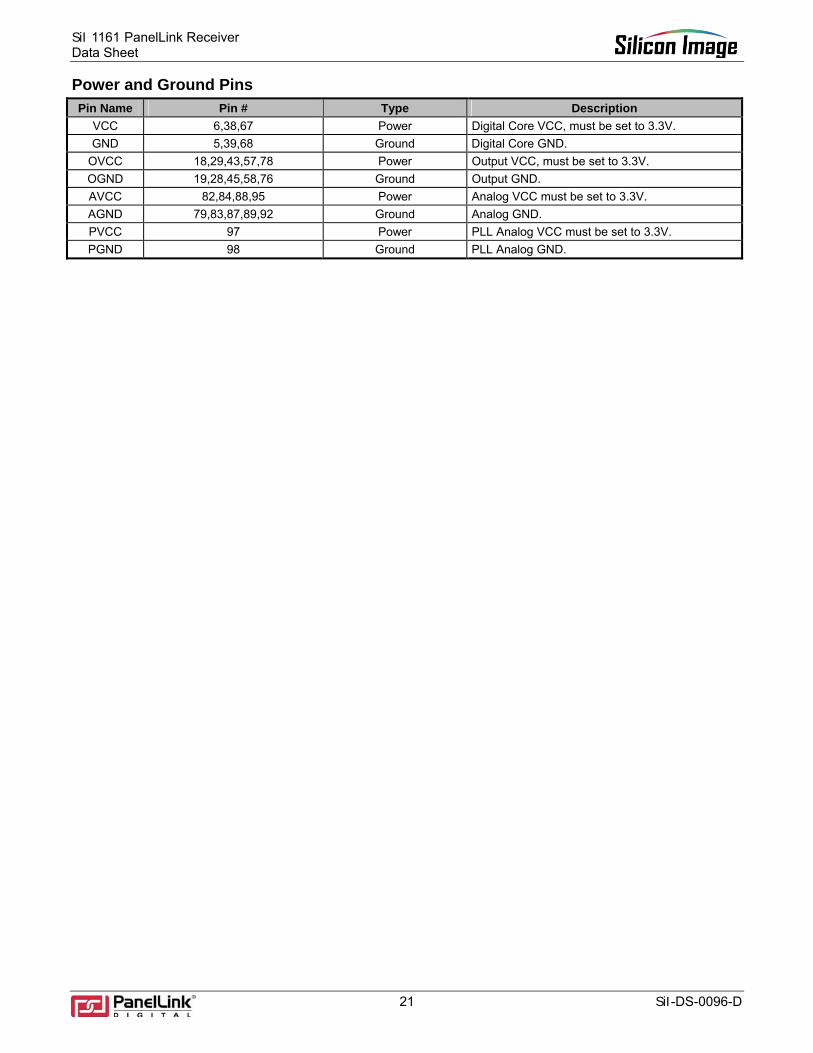
Power and Ground Pins Pin Name Pin # Type Description
VCC 6,38,67 Power Digital Core VCC, must be set to 3.3V. GND 5,39,68 Ground Digital Core GND.
OVCC 18,29,43,57,78 Power Output VCC, must be set to 3.3V. OGND 19,28,45,58,76 Ground Output GND. AVCC 82,84,88,95 Power Analog VCC must be set to 3.3V. AGND 79,83,87,89,92 Ground Analog GND. PVCC 97 Power PLL Analog VCC must be set to 3.3V. PGND 98 Ground PLL Analog GND.
SiI 1161 PanelLink ReceiverData Sheet
SiI-DS-0096-D 22
Feature Information
HSYNC De-jitter Function HSYNC de-jitter enables the SiI 1161 to operate properly even when the HSYNC signal contains jitter. Pin 1 is used to enable or disable this circuit. Tying this pin high enables the HSYNC de-jitter circuitry while tying it low disables the circuitry. The HSYNC de-jitter circuitry operates normally with most VESA standard timings. In most modes, HSYNC and VSYNC total times and front and back porch times are multiples of four pixel times. If the timings are not a multiple of four, operation is not guaranteed and the HSYNC de-jitter circuitry should be turned off. When HSYNC de-jitter is enabled, the circuitry will introduce anywhere from 1 to 4 CLK delays in the HSYNC signal relative to the output data.
Clock Detect Function The SiI 1161 includes a power saving feature: power down with clock detect circuit. The SiI 1161 will go into a low power mode when there is no video clock coming from the transmitter. In this mode, the entire chip is powered down except the clock detect circuitry. During this mode, digital I/O are set to a high impedance (tri-state) mode. The SCDT pin is driven LOW. A weak internal pull-down device brings each output to ground. The device power down and wake-up times are shown in Figure 11 and Figure 12.
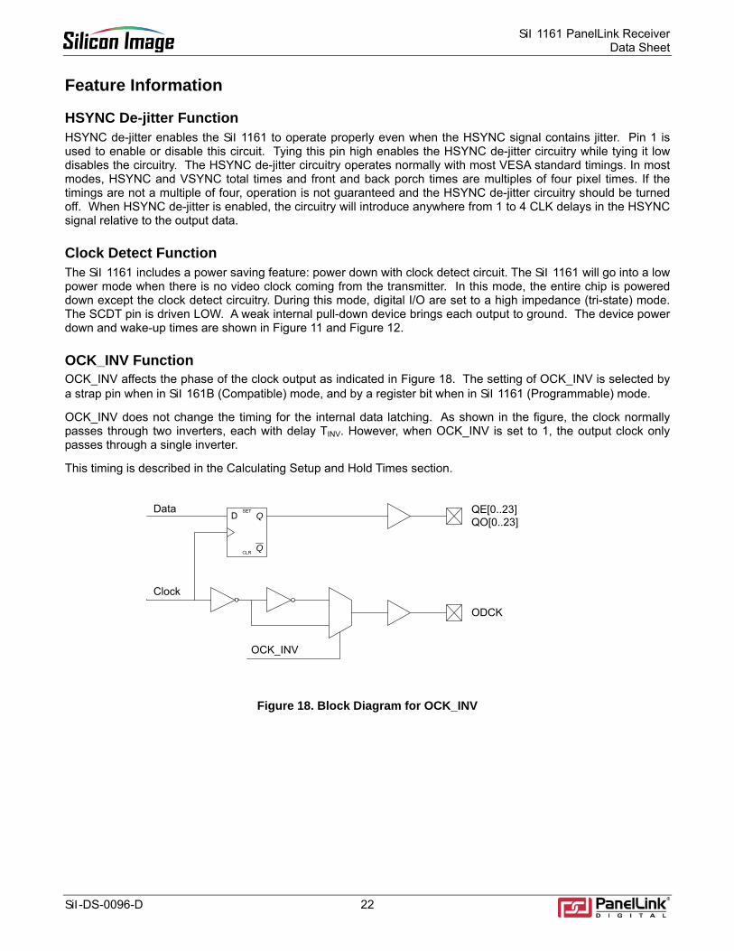
OCK_INV Function OCK_INV affects the phase of the clock output as indicated in Figure 18. The setting of OCK_INV is selected by a strap pin when in SiI 161B (Compatible) mode, and by a register bit when in SiI 1161 (Programmable) mode.
OCK_INV does not change the timing for the internal data latching. As shown in the figure, the clock normally passes through two inverters, each with delay TINV. However, when OCK_INV is set to 1, the output clock only passes through a single inverter.
This timing is described in the Calculating Setup and Hold Times section.
Figure 18. Block Diagram for OCK_INV
Q
QSET
CLR
DData
Clock
OCK_INV
QE[0..23]QO[0..23]
ODCK
SiI 1161 PanelLink Receiver Data Sheet
23 SiI-DS-0096-D
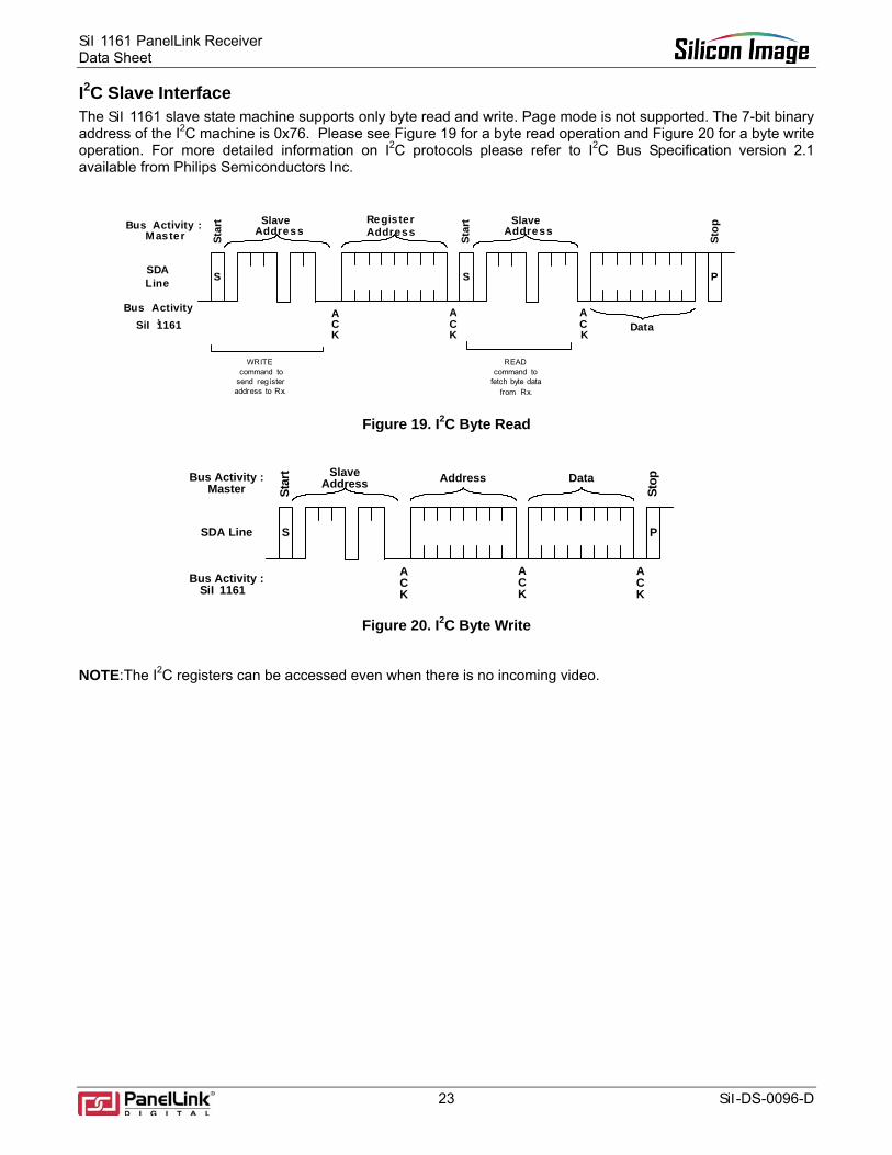
I2C Slave Interface The SiI 1161 slave state machine supports only byte read and write. Page mode is not supported. The 7-bit binary address of the I2C machine is 0x76. Please see Figure 19 for a byte read operation and Figure 20 for a byte write operation. For more detailed information on I2C protocols please refer to I2C Bus Specification version 2.1 available from Philips Semiconductors Inc.
S
ACK
S
ACK
ACK
P
SlaveAddress
RegisterAddress
Data
Stop
Star
t
Star
t
Bus Activity:SiI 1161
Bus Activity :Master
SDALine
SlaveAddress
WRITEcommand to
send registeraddress to Rx.
READcommand to
fetch byte datafrom Rx.
Figure 19. I2C Byte Read
S
ACK
ACK
P
SlaveAddress Address Data
Stop
Star
t
Bus Activity :SiI 1161
Bus Activity :Master
SDA Line
ACK
Figure 20. I2C Byte Write
NOTE: The I2C registers can be accessed even when there is no incoming video.
SiI 1161 PanelLink ReceiverData Sheet
SiI-DS-0096-D 24
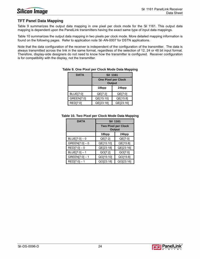
TFT Panel Data Mapping Table 9 summarizes the output data mapping in one pixel per clock mode for the SiI 1161. This output data mapping is dependent upon the PanelLink transmitters having the exact same type of input data mappings.
Table 10 summarizes the output data mapping in two pixels per clock mode. More detailed mapping information is found on the following pages. Refer to application note SiI-AN-0007 for DSTN applications.
Note that the data configuration of the receiver is independent of the configuration of the transmitter. The data is always transmitted across the link in the same format, regardless of the selection of 12, 24 or 48 bit input format. Therefore, display-side designers do not need to know how the transmitter is configured. Receiver configuration is for compatibility with the display, not the transmitter.
Table 9. One Pixel per Clock Mode Data Mapping
SiI 1161DATA One Pixel per Clock
Output
18bpp 24bpp
BLUE[7:0] QE[7:2] QE[7:0] GREEN[7:0] QE[15:10] QE[15:8] RED[7:0] QE[23:18] QE[23:16]
Table 10. Two Pixel per Clock Mode Data Mapping SiI 1161DATA
Two Pixel per Clock Output
18bpp 24bpp BLUE[7:0] – 0 QE[7:2] QE[7:0] GREEN[7:0] – 0 QE[15:10] QE[15:8] RED[7:0] – 0 QE[23:18] QE[23:16] BLUE[7:0] – 1 QO[7:2] QO[7:0] GREEN[7:0] – 1 QO[15:10] QO[15:8] RED[7:0] – 1 QO[23:18] QO[23:16]
SiI 1161 PanelLink Receiver Data Sheet
25 SiI-DS-0096-D
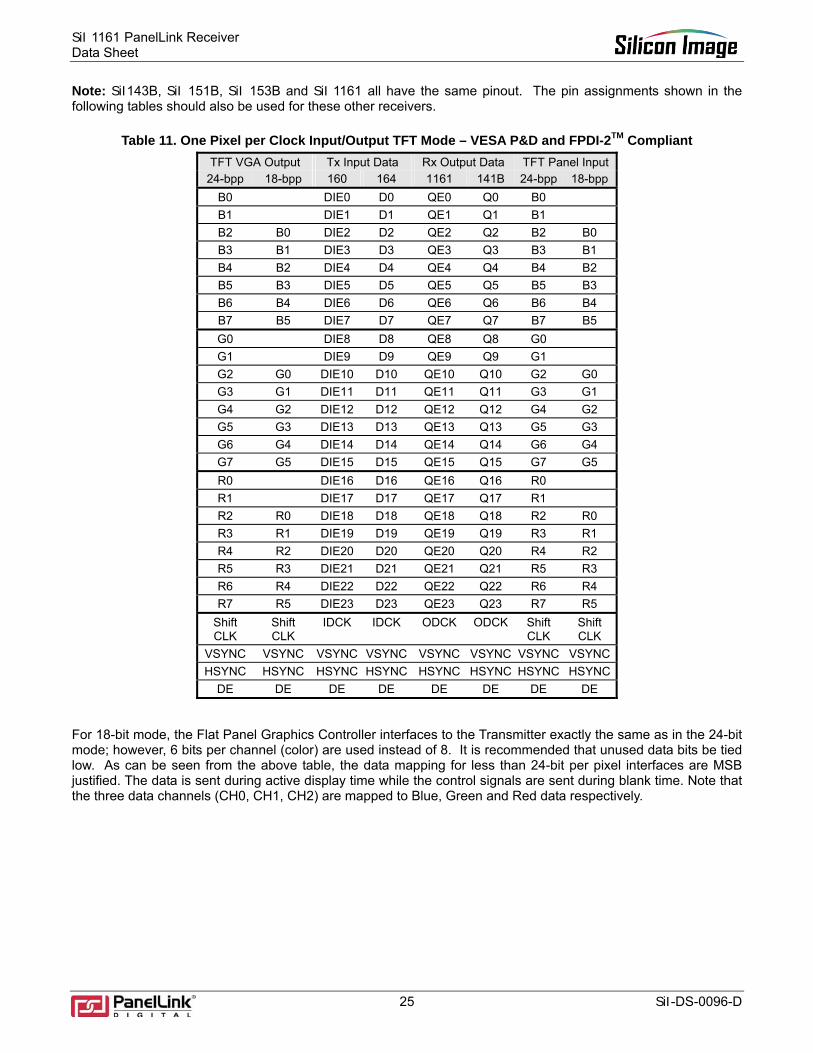
Note: SiI143B, SiI 151B, SiI 153B and SiI 1161 all have the same pinout. The pin assignments shown in the following tables should also be used for these other receivers.
Table 11. One Pixel per Clock Input/Output TFT Mode – VESA P&D and FPDI-2TM Compliant TFT VGA Output Tx Input Data Rx Output Data TFT Panel Input
24-bpp 18-bpp 160 164 1161 141B 24-bpp 18-bpp B0 DIE0 D0 QE0 Q0 B0 B1 DIE1 D1 QE1 Q1 B1 B2 B0 DIE2 D2 QE2 Q2 B2 B0 B3 B1 DIE3 D3 QE3 Q3 B3 B1 B4 B2 DIE4 D4 QE4 Q4 B4 B2 B5 B3 DIE5 D5 QE5 Q5 B5 B3 B6 B4 DIE6 D6 QE6 Q6 B6 B4 B7 B5 DIE7 D7 QE7 Q7 B7 B5 G0 DIE8 D8 QE8 Q8 G0 G1 DIE9 D9 QE9 Q9 G1 G2 G0 DIE10 D10 QE10 Q10 G2 G0 G3 G1 DIE11 D11 QE11 Q11 G3 G1 G4 G2 DIE12 D12 QE12 Q12 G4 G2 G5 G3 DIE13 D13 QE13 Q13 G5 G3 G6 G4 DIE14 D14 QE14 Q14 G6 G4 G7 G5 DIE15 D15 QE15 Q15 G7 G5 R0 DIE16 D16 QE16 Q16 R0 R1 DIE17 D17 QE17 Q17 R1 R2 R0 DIE18 D18 QE18 Q18 R2 R0 R3 R1 DIE19 D19 QE19 Q19 R3 R1 R4 R2 DIE20 D20 QE20 Q20 R4 R2 R5 R3 DIE21 D21 QE21 Q21 R5 R3 R6 R4 DIE22 D22 QE22 Q22 R6 R4 R7 R5 DIE23 D23 QE23 Q23 R7 R5
Shift CLK
Shift CLK
IDCK IDCK ODCK ODCK Shift CLK
Shift CLK
VSYNC VSYNC VSYNC VSYNC VSYNC VSYNC VSYNC VSYNC HSYNC HSYNC HSYNC HSYNC HSYNC HSYNC HSYNC HSYNC
DE DE DE DE DE DE DE DE For 18-bit mode, the Flat Panel Graphics Controller interfaces to the Transmitter exactly the same as in the 24-bit mode; however, 6 bits per channel (color) are used instead of 8. It is recommended that unused data bits be tied low. As can be seen from the above table, the data mapping for less than 24-bit per pixel interfaces are MSB justified. The data is sent during active display time while the control signals are sent during blank time. Note that the three data channels (CH0, CH1, CH2) are mapped to Blue, Green and Red data respectively.
SiI 1161 PanelLink ReceiverData Sheet
SiI-DS-0096-D 26
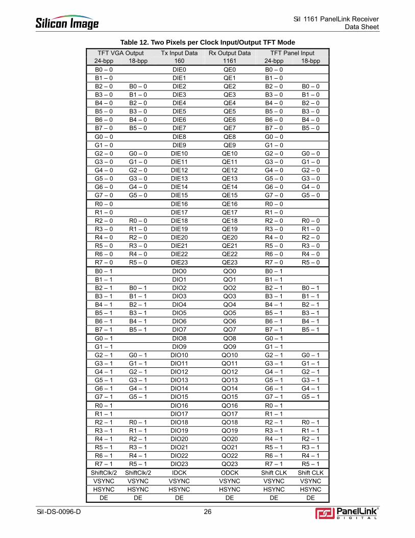
Table 12. Two Pixels per Clock Input/Output TFT Mode TFT VGA Output Tx Input Data Rx Output Data TFT Panel Input
24-bpp 18-bpp 160 1161 24-bpp 18-bpp B0 – 0 DIE0 QE0 B0 – 0 B1 – 0 DIE1 QE1 B1 – 0 B2 – 0 B0 – 0 DIE2 QE2 B2 – 0 B0 – 0 B3 – 0 B1 – 0 DIE3 QE3 B3 – 0 B1 – 0 B4 – 0 B2 – 0 DIE4 QE4 B4 – 0 B2 – 0 B5 – 0 B3 – 0 DIE5 QE5 B5 – 0 B3 – 0 B6 – 0 B4 – 0 DIE6 QE6 B6 – 0 B4 – 0 B7 – 0 B5 – 0 DIE7 QE7 B7 – 0 B5 – 0 G0 – 0 DIE8 QE8 G0 – 0 G1 – 0 DIE9 QE9 G1 – 0 G2 – 0 G0 – 0 DIE10 QE10 G2 – 0 G0 – 0 G3 – 0 G1 – 0 DIE11 QE11 G3 – 0 G1 – 0 G4 – 0 G2 – 0 DIE12 QE12 G4 – 0 G2 – 0 G5 – 0 G3 – 0 DIE13 QE13 G5 – 0 G3 – 0 G6 – 0 G4 – 0 DIE14 QE14 G6 – 0 G4 – 0 G7 – 0 G5 – 0 DIE15 QE15 G7 – 0 G5 – 0 R0 – 0 DIE16 QE16 R0 – 0 R1 – 0 DIE17 QE17 R1 – 0 R2 – 0 R0 – 0 DIE18 QE18 R2 – 0 R0 – 0 R3 – 0 R1 – 0 DIE19 QE19 R3 – 0 R1 – 0 R4 – 0 R2 – 0 DIE20 QE20 R4 – 0 R2 – 0 R5 – 0 R3 – 0 DIE21 QE21 R5 – 0 R3 – 0 R6 – 0 R4 – 0 DIE22 QE22 R6 – 0 R4 – 0 R7 – 0 R5 – 0 DIE23 QE23 R7 – 0 R5 – 0 B0 – 1 DIO0 QO0 B0 – 1 B1 – 1 DIO1 QO1 B1 – 1 B2 – 1 B0 – 1 DIO2 QO2 B2 – 1 B0 – 1 B3 – 1 B1 – 1 DIO3 QO3 B3 – 1 B1 – 1 B4 – 1 B2 – 1 DIO4 QO4 B4 – 1 B2 – 1 B5 – 1 B3 – 1 DIO5 QO5 B5 – 1 B3 – 1 B6 – 1 B4 – 1 DIO6 QO6 B6 – 1 B4 – 1 B7 – 1 B5 – 1 DIO7 QO7 B7 – 1 B5 – 1 G0 – 1 DIO8 QO8 G0 – 1 G1 – 1 DIO9 QO9 G1 – 1 G2 – 1 G0 – 1 DIO10 QO10 G2 – 1 G0 – 1 G3 – 1 G1 – 1 DIO11 QO11 G3 – 1 G1 – 1 G4 – 1 G2 – 1 DIO12 QO12 G4 – 1 G2 – 1 G5 – 1 G3 – 1 DIO13 QO13 G5 – 1 G3 – 1 G6 – 1 G4 – 1 DIO14 QO14 G6 – 1 G4 – 1 G7 – 1 G5 – 1 DIO15 QO15 G7 – 1 G5 – 1 R0 – 1 DIO16 QO16 R0 – 1 R1 – 1 DIO17 QO17 R1 – 1 R2 – 1 R0 – 1 DIO18 QO18 R2 – 1 R0 – 1 R3 – 1 R1 – 1 DIO19 QO19 R3 – 1 R1 – 1 R4 – 1 R2 – 1 DIO20 QO20 R4 – 1 R2 – 1 R5 – 1 R3 – 1 DIO21 QO21 R5 – 1 R3 – 1 R6 – 1 R4 – 1 DIO22 QO22 R6 – 1 R4 – 1 R7 – 1 R5 – 1 DIO23 QO23 R7 – 1 R5 – 1
ShiftClk/2 ShiftClk/2 IDCK ODCK Shift CLK Shift CLK VSYNC VSYNC VSYNC VSYNC VSYNC VSYNC HSYNC HSYNC HSYNC HSYNC HSYNC HSYNC
DE DE DE DE DE DE
SiI 1161 PanelLink Receiver Data Sheet
27 SiI-DS-0096-D
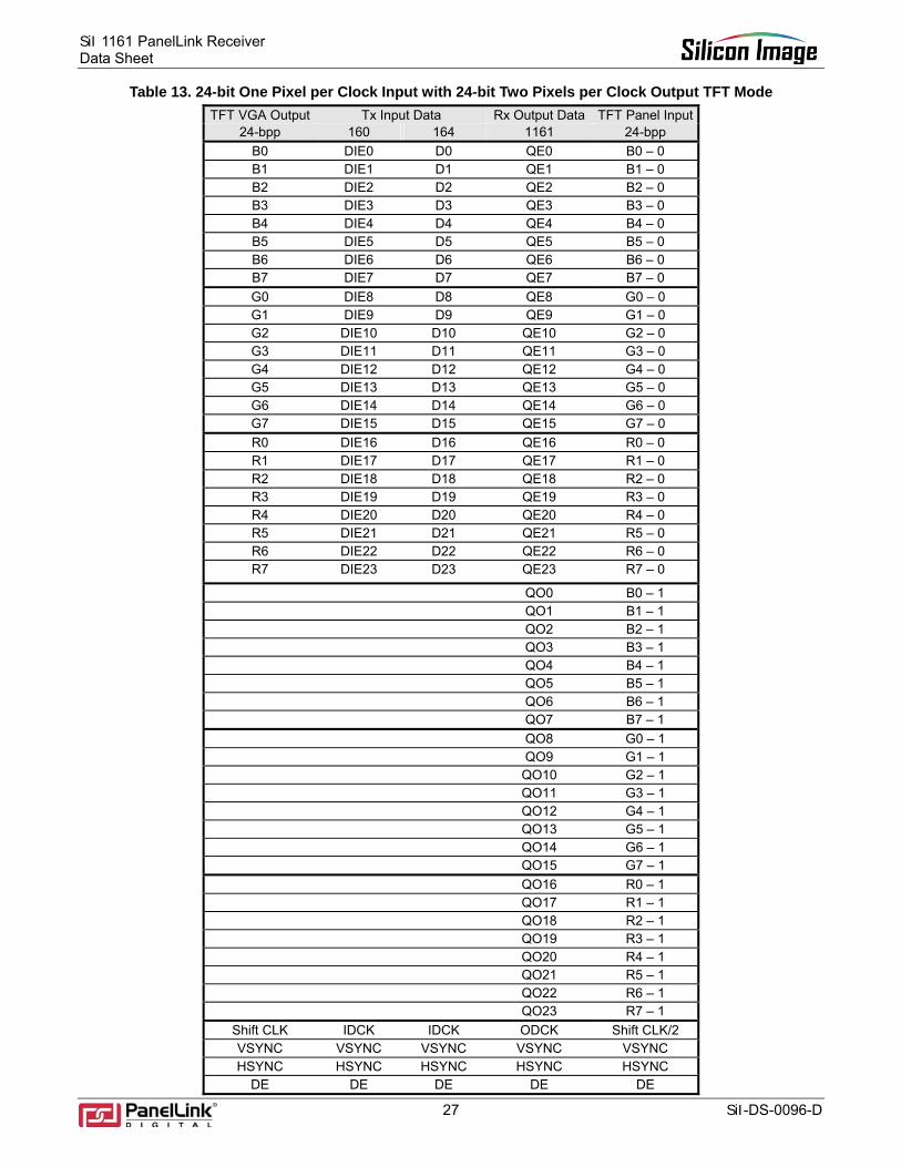
Table 13. 24-bit One Pixel per Clock Input with 24-bit Two Pixels per Clock Output TFT Mode TFT VGA Output Tx Input Data Rx Output Data TFT Panel Input
24-bpp 160 164 1161 24-bpp B0 DIE0 D0 QE0 B0 – 0 B1 DIE1 D1 QE1 B1 – 0 B2 DIE2 D2 QE2 B2 – 0 B3 DIE3 D3 QE3 B3 – 0 B4 DIE4 D4 QE4 B4 – 0 B5 DIE5 D5 QE5 B5 – 0 B6 DIE6 D6 QE6 B6 – 0 B7 DIE7 D7 QE7 B7 – 0 G0 DIE8 D8 QE8 G0 – 0 G1 DIE9 D9 QE9 G1 – 0 G2 DIE10 D10 QE10 G2 – 0 G3 DIE11 D11 QE11 G3 – 0 G4 DIE12 D12 QE12 G4 – 0 G5 DIE13 D13 QE13 G5 – 0 G6 DIE14 D14 QE14 G6 – 0 G7 DIE15 D15 QE15 G7 – 0 R0 DIE16 D16 QE16 R0 – 0 R1 DIE17 D17 QE17 R1 – 0 R2 DIE18 D18 QE18 R2 – 0 R3 DIE19 D19 QE19 R3 – 0 R4 DIE20 D20 QE20 R4 – 0 R5 DIE21 D21 QE21 R5 – 0 R6 DIE22 D22 QE22 R6 – 0 R7 DIE23 D23 QE23 R7 – 0
QO0 B0 – 1 QO1 B1 – 1 QO2 B2 – 1 QO3 B3 – 1 QO4 B4 – 1 QO5 B5 – 1 QO6 B6 – 1 QO7 B7 – 1 QO8 G0 – 1 QO9 G1 – 1 QO10 G2 – 1 QO11 G3 – 1 QO12 G4 – 1 QO13 G5 – 1 QO14 G6 – 1 QO15 G7 – 1 QO16 R0 – 1 QO17 R1 – 1 QO18 R2 – 1 QO19 R3 – 1 QO20 R4 – 1 QO21 R5 – 1 QO22 R6 – 1 QO23 R7 – 1
Shift CLK IDCK IDCK ODCK Shift CLK/2 VSYNC VSYNC VSYNC VSYNC VSYNC HSYNC HSYNC HSYNC HSYNC HSYNC
DE DE DE DE DE
SiI 1161 PanelLink ReceiverData Sheet
SiI-DS-0096-D 28
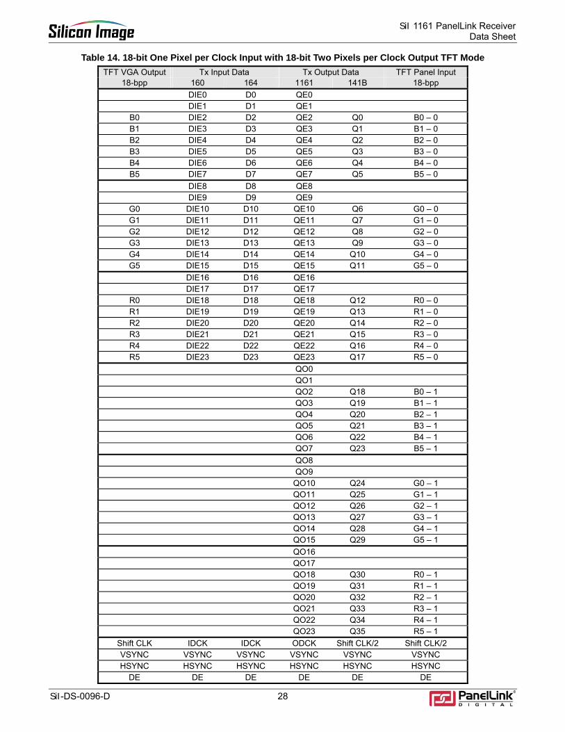
Table 14. 18-bit One Pixel per Clock Input with 18-bit Two Pixels per Clock Output TFT Mode TFT VGA Output Tx Input Data Tx Output Data TFT Panel Input
18-bpp 160 164 1161 141B 18-bpp DIE0 D0 QE0 DIE1 D1 QE1
B0 DIE2 D2 QE2 Q0 B0 – 0 B1 DIE3 D3 QE3 Q1 B1 – 0 B2 DIE4 D4 QE4 Q2 B2 – 0 B3 DIE5 D5 QE5 Q3 B3 – 0 B4 DIE6 D6 QE6 Q4 B4 – 0 B5 DIE7 D7 QE7 Q5 B5 – 0
DIE8 D8 QE8 DIE9 D9 QE9
G0 DIE10 D10 QE10 Q6 G0 – 0 G1 DIE11 D11 QE11 Q7 G1 – 0 G2 DIE12 D12 QE12 Q8 G2 – 0 G3 DIE13 D13 QE13 Q9 G3 – 0 G4 DIE14 D14 QE14 Q10 G4 – 0 G5 DIE15 D15 QE15 Q11 G5 – 0
DIE16 D16 QE16 DIE17 D17 QE17
R0 DIE18 D18 QE18 Q12 R0 – 0 R1 DIE19 D19 QE19 Q13 R1 – 0 R2 DIE20 D20 QE20 Q14 R2 – 0 R3 DIE21 D21 QE21 Q15 R3 – 0 R4 DIE22 D22 QE22 Q16 R4 – 0 R5 DIE23 D23 QE23 Q17 R5 – 0
QO0 QO1 QO2 Q18 B0 – 1 QO3 Q19 B1 – 1 QO4 Q20 B2 – 1 QO5 Q21 B3 – 1 QO6 Q22 B4 – 1 QO7 Q23 B5 – 1 QO8 QO9 QO10 Q24 G0 – 1 QO11 Q25 G1 – 1 QO12 Q26 G2 – 1 QO13 Q27 G3 – 1 QO14 Q28 G4 – 1 QO15 Q29 G5 – 1 QO16 QO17 QO18 Q30 R0 – 1 QO19 Q31 R1 – 1 QO20 Q32 R2 – 1 QO21 Q33 R3 – 1 QO22 Q34 R4 – 1 QO23 Q35 R5 – 1
Shift CLK IDCK IDCK ODCK Shift CLK/2 Shift CLK/2 VSYNC VSYNC VSYNC VSYNC VSYNC VSYNC HSYNC HSYNC HSYNC HSYNC HSYNC HSYNC
DE DE DE DE DE DE
SiI 1161 PanelLink Receiver Data Sheet
29 SiI-DS-0096-D
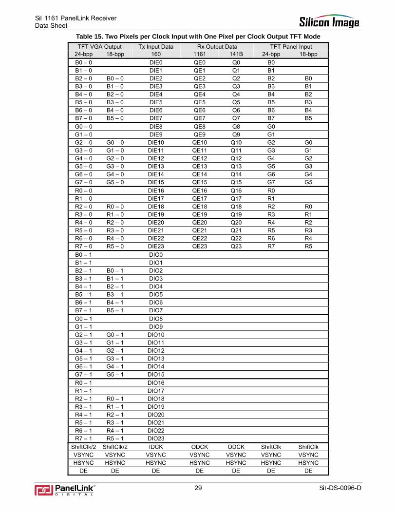
Table 15. Two Pixels per Clock Input with One Pixel per Clock Output TFT Mode TFT VGA Output Tx Input Data Rx Output Data TFT Panel Input
24-bpp 18-bpp 160 1161 141B 24-bpp 18-bpp B0 – 0 DIE0 QE0 Q0 B0 B1 – 0 DIE1 QE1 Q1 B1 B2 – 0 B0 – 0 DIE2 QE2 Q2 B2 B0 B3 – 0 B1 – 0 DIE3 QE3 Q3 B3 B1 B4 – 0 B2 – 0 DIE4 QE4 Q4 B4 B2 B5 – 0 B3 – 0 DIE5 QE5 Q5 B5 B3 B6 – 0 B4 – 0 DIE6 QE6 Q6 B6 B4 B7 – 0 B5 – 0 DIE7 QE7 Q7 B7 B5 G0 – 0 DIE8 QE8 Q8 G0 G1 – 0 DIE9 QE9 Q9 G1 G2 – 0 G0 – 0 DIE10 QE10 Q10 G2 G0 G3 – 0 G1 – 0 DIE11 QE11 Q11 G3 G1 G4 – 0 G2 – 0 DIE12 QE12 Q12 G4 G2 G5 – 0 G3 – 0 DIE13 QE13 Q13 G5 G3 G6 – 0 G4 – 0 DIE14 QE14 Q14 G6 G4 G7 – 0 G5 – 0 DIE15 QE15 Q15 G7 G5 R0 – 0 DIE16 QE16 Q16 R0 R1 – 0 DIE17 QE17 Q17 R1 R2 – 0 R0 – 0 DIE18 QE18 Q18 R2 R0 R3 – 0 R1 – 0 DIE19 QE19 Q19 R3 R1 R4 – 0 R2 – 0 DIE20 QE20 Q20 R4 R2 R5 – 0 R3 – 0 DIE21 QE21 Q21 R5 R3 R6 – 0 R4 – 0 DIE22 QE22 Q22 R6 R4 R7 – 0 R5 – 0 DIE23 QE23 Q23 R7 R5 B0 – 1 DIO0 B1 – 1 DIO1 B2 – 1 B0 – 1 DIO2 B3 – 1 B1 – 1 DIO3 B4 – 1 B2 – 1 DIO4 B5 – 1 B3 – 1 DIO5 B6 – 1 B4 – 1 DIO6 B7 – 1 B5 – 1 DIO7 G0 – 1 DIO8 G1 – 1 DIO9 G2 – 1 G0 – 1 DIO10 G3 – 1 G1 – 1 DIO11 G4 – 1 G2 – 1 DIO12 G5 – 1 G3 – 1 DIO13 G6 – 1 G4 – 1 DIO14 G7 – 1 G5 – 1 DIO15 R0 – 1 DIO16 R1 – 1 DIO17 R2 – 1 R0 – 1 DIO18 R3 – 1 R1 – 1 DIO19 R4 – 1 R2 – 1 DIO20 R5 – 1 R3 – 1 DIO21 R6 – 1 R4 – 1 DIO22 R7 – 1 R5 – 1 DIO23
ShiftClk/2 ShiftClk/2 IDCK ODCK ODCK ShiftClk ShiftClk VSYNC VSYNC VSYNC VSYNC VSYNC VSYNC VSYNC HSYNC HSYNC HSYNC HSYNC HSYNC HSYNC HSYNC
DE DE DE DE DE DE DE
SiI 1161 PanelLink ReceiverData Sheet
SiI-DS-0096-D 30
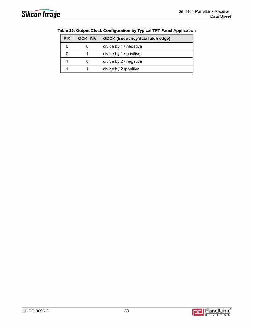
Table 16. Output Clock Configuration by Typical TFT Panel Application
PIX OCK_INV ODCK (frequency/data latch edge)
0 0 divide by 1 / negative
0 1 divide by 1 / positive
1 0 divide by 2 / negative
1 1 divide by 2 /positive
SiI 1161 PanelLink Receiver Data Sheet
31 SiI-DS-0096-D
Design Recommendations The following sections describe recommendations for robust board design with this PanelLink receiver. Designers should include provision for these circuits in their design, and adjust the specific passive component values according to the characterization results.
Differences Between SiI 161B and SiI 1161 The RESERVED pin (pin 99) on the SiI 161B is required to be tied HIGH for normal operation. On the SiI 1161 part, pin 99 is defined so that tying it HIGH maintains pin compatibility with the SiI 161B. In this mode, the SiI 1611 chip meets all operational and timing specifications of the SiI 161B with these exceptions.
Active mode power consumption is higher on the SiI 1161 part due to the new equalizer circuitry. Refer to Table 1 for actual values.
TFSC is shorter and more predictable due to improved logic implementation.
Selecting SiI 1161 (Programmable) Mode To use the programmable features of the SiI 1161 part:
Tie pin 99 (the MODE signal) LOW
Tie pin 7 (the I2C_MODE# signal) LOW
The chipset registers are now accessible through standard I2C signaling up to 400kHz through pins 3 (SDA) and 100 (SCL). Note that these pins must be connected through pullups (2kΩ recommended) to 3.3V for correct operation. In this mode, several pins change their functionality from the SiI 161B standard as shown in Table 17.
Table 17. New Pin Functions for SiI 1161 in Programmable Mode Pin MODE tied HIGH MODE tied LOW 99 Chip is in SiI 161B Compatible Mode Chip is in SiI 1161 I2C Programmable Mode 7 STAG_OUT# I2C_MODE#
HIGH: Not Supported LOW: Chip is in I2C Programmable Mode
3 ST SDA 100 OCK_INV SCL
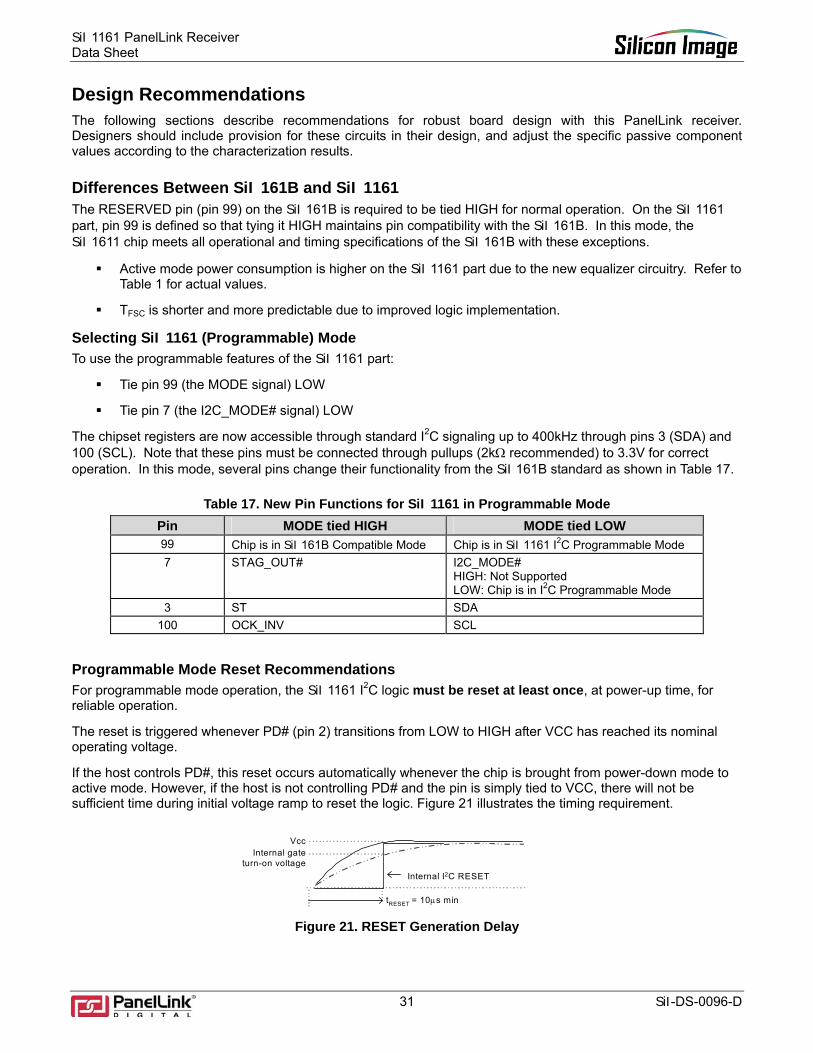
Programmable Mode Reset Recommendations For programmable mode operation, the SiI 1161 I2C logic must be reset at least once, at power-up time, for reliable operation.
The reset is triggered whenever PD# (pin 2) transitions from LOW to HIGH after VCC has reached its nominal operating voltage.
If the host controls PD#, this reset occurs automatically whenever the chip is brought from power-down mode to active mode. However, if the host is not controlling PD# and the pin is simply tied to VCC, there will not be sufficient time during initial voltage ramp to reset the logic. Figure 21 illustrates the timing requirement.
Figure 21. RESET Generation Delay
VccInternal gate
turn-on voltageInternal I2C RESET
tRESET = 10µs min
SiI 1161 PanelLink ReceiverData Sheet
SiI-DS-0096-D 32
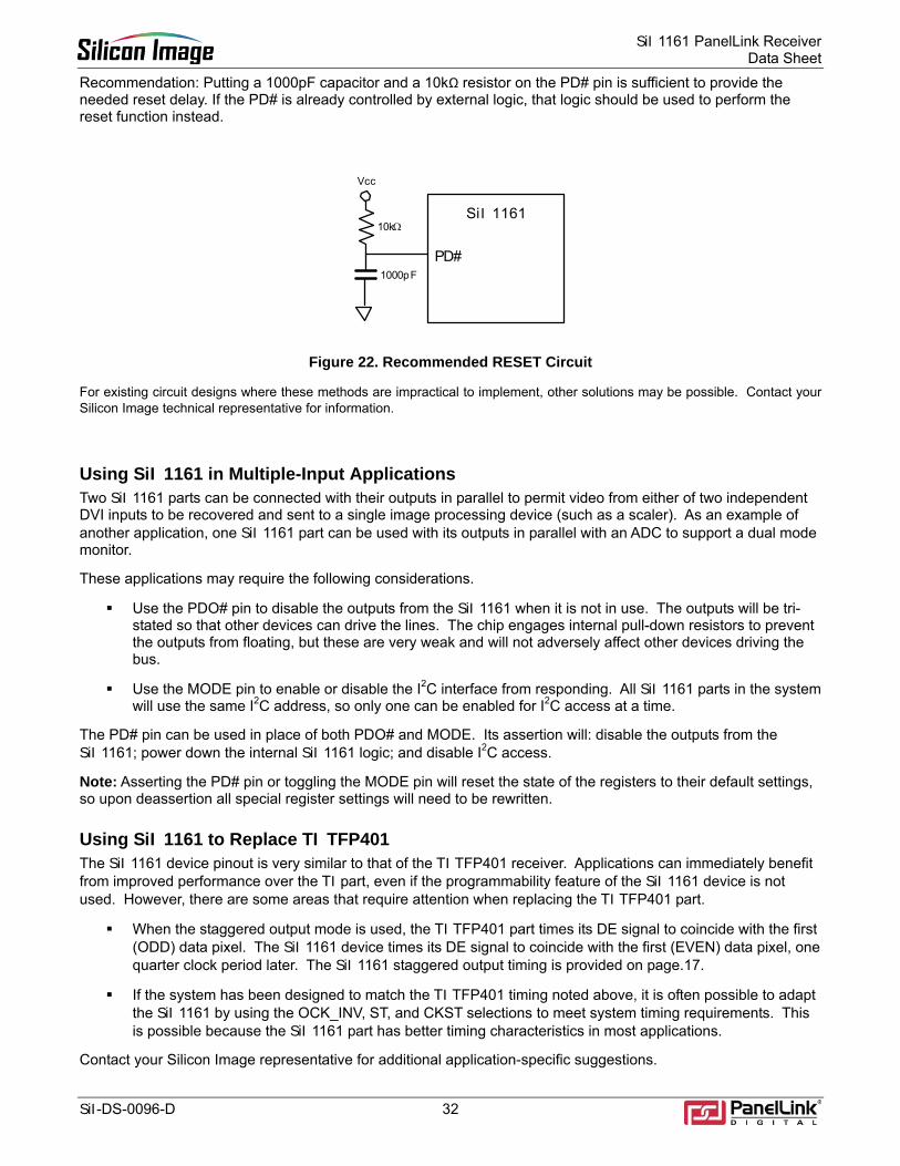
Recommendation: Putting a 1000pF capacitor and a 10kΩ resistor on the PD# pin is sufficient to provide the needed reset delay. If the PD# is already controlled by external logic, that logic should be used to perform the reset function instead.
Vcc
10kΩ
1000pFPD#
SiI 1161
Figure 22. Recommended RESET Circuit
For existing circuit designs where these methods are impractical to implement, other solutions may be possible. Contact your Silicon Image technical representative for information.
Using SiI 1161 in Multiple-Input Applications Two SiI 1161 parts can be connected with their outputs in parallel to permit video from either of two independent DVI inputs to be recovered and sent to a single image processing device (such as a scaler). As an example of another application, one SiI 1161 part can be used with its outputs in parallel with an ADC to support a dual mode monitor.
These applications may require the following considerations.
Use the PDO# pin to disable the outputs from the SiI 1161 when it is not in use. The outputs will be tri-stated so that other devices can drive the lines. The chip engages internal pull-down resistors to prevent the outputs from floating, but these are very weak and will not adversely affect other devices driving the bus.
Use the MODE pin to enable or disable the I2C interface from responding. All SiI 1161 parts in the system will use the same I2C address, so only one can be enabled for I2C access at a time.
The PD# pin can be used in place of both PDO# and MODE. Its assertion will: disable the outputs from the SiI 1161; power down the internal SiI 1161 logic; and disable I2C access.
Note: Asserting the PD# pin or toggling the MODE pin will reset the state of the registers to their default settings, so upon deassertion all special register settings will need to be rewritten.
Using SiI 1161 to Replace TI TFP401 The SiI 1161 device pinout is very similar to that of the TI TFP401 receiver. Applications can immediately benefit from improved performance over the TI part, even if the programmability feature of the SiI 1161 device is not used. However, there are some areas that require attention when replacing the TI TFP401 part.
When the staggered output mode is used, the TI TFP401 part times its DE signal to coincide with the first (ODD) data pixel. The SiI 1161 device times its DE signal to coincide with the first (EVEN) data pixel, one quarter clock period later. The SiI 1161 staggered output timing is provided on page.17.
If the system has been designed to match the TI TFP401 timing noted above, it is often possible to adapt the SiI 1161 by using the OCK_INV, ST, and CKST selections to meet system timing requirements. This is possible because the SiI 1161 part has better timing characteristics in most applications.
Contact your Silicon Image representative for additional application-specific suggestions.
SiI 1161 PanelLink Receiver Data Sheet
33 SiI-DS-0096-D
Adjusting Equalizer and Bandwidth The SiI 1161 provides access to several internal registers that can be set to optimize the connection to a variety of source devices and accommodate a range of cable lengths.
The SiI 1161 provides access to several internal registers that can be set to optimize the connection to a variety of source devices and accommodate a range of cable lengths. Pins must be set in Programmable Mode according to the details shown in Table 17 on page 31. The rules for setting the registers for best operation are flexible; the only goal is to achieve best visual performance on the display. In general these guidelines apply.
The EQ_DATA bits correspond to the cable length, with 0000 applying to the longest cables, and 1111 applying to the shortest cables. Cable quality and DVI signal source quality also factor into this setting, so there is no exact correspondence of settings to cable length. With good cable quality and a fully DVI-compliant source, cable lengths of 20m are achievable at UXGA.
The LBW bits correspond to the clock recovery PLL bandwidth. DVI-compliant transmitters are best accommodated by a setting of 4MHz as dictated by the DVI 1.0 spec. Recovery of data from non DVI-compliant transmitters is often better when the bandwidth is set to a higher value. Refer to Table 19 for setting information.
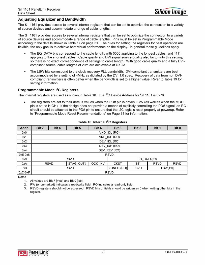
Programmable Mode I2C Registers The internal registers are used as shown in Table 18. The I2C Device Address for SiI 1161 is 0x76.
• The registers are set to their default values when the PD# pin is driven LOW (as well as when the MODE pin is set to HIGH). If the design does not provide a means of explicitly controlling the PD# signal, an RC circuit should be attached to the PD# pin to ensure that the I2C logic is reset properly at powerup. Refer to “Programmable Mode Reset Recommendations” on Page 31 for information.
Table 18. Internal I2C Registers Addr. Bit 7 Bit 6 Bit 5 Bit 4 Bit 3 Bit 2 Bit 1 Bit 0
0x0 VND_IDL (RO) 0x1 VND_IDH (RO) 0x2 DEV_IDL (RO) 0x3 DEV_IDH (RO) 0x4 DEV_REV (RO)
0x5-0x8 RSVD 0x9 RSVD EQ_DATA[3:0] 0xA RSVD STAG_OUT# OCK_INV CKST ST RSVD RSVD 0xB RSVD ZONEO (RO) RSVD LBW[1:0]
0xC-0xF RSVD Notes
1. All values are Bit 7 [msb] and Bit 0 [lsb]. 2. RW (or unmarked) indicates a read/write field. RO indicates a read-only field. 3. RSVD registers should not be accessed. RSVD bits or fields should be written as 0 when writing other bits in the
register.
SiI 1161 PanelLink ReceiverData Sheet
SiI-DS-0096-D 34
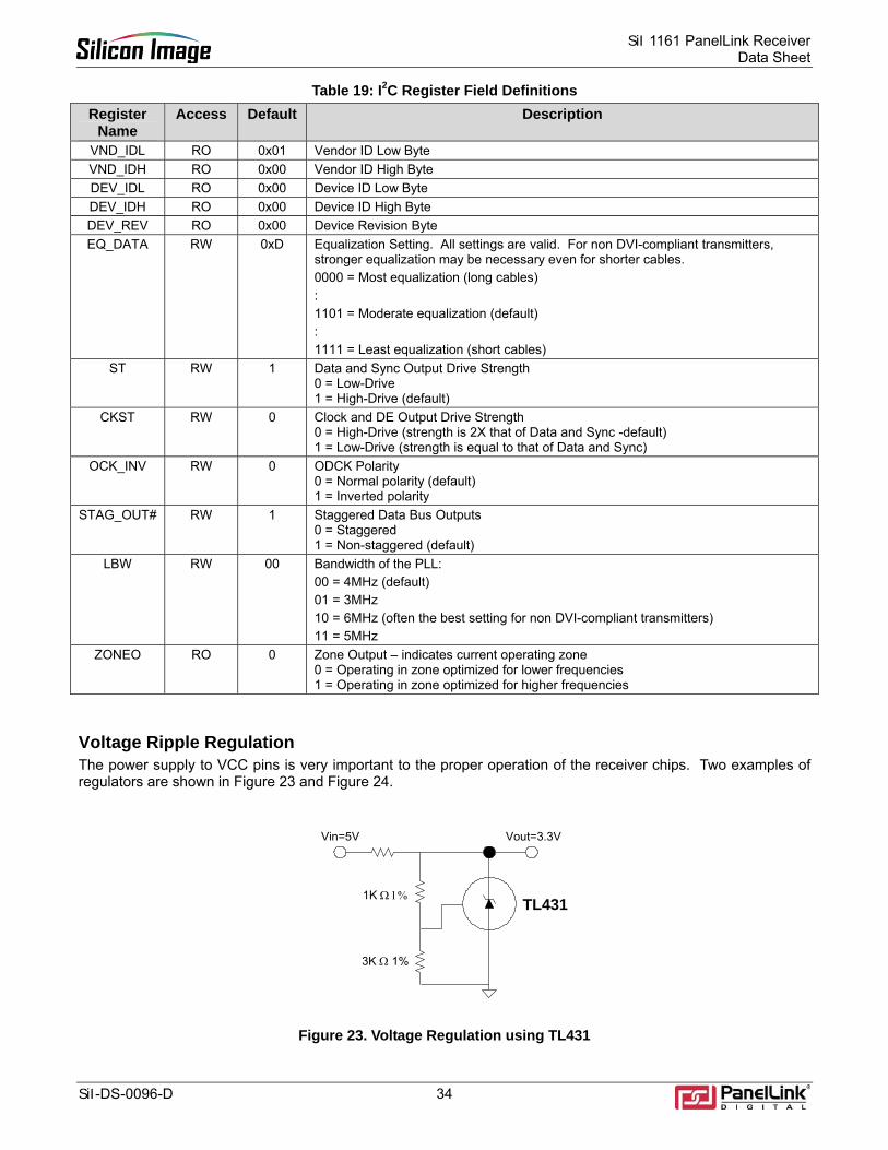
Table 19: I2C Register Field Definitions Register
Name Access Default Description
VND_IDL RO 0x01 Vendor ID Low Byte VND_IDH RO 0x00 Vendor ID High Byte DEV_IDL RO 0x00 Device ID Low Byte DEV_IDH RO 0x00 Device ID High Byte DEV_REV RO 0x00 Device Revision Byte EQ_DATA RW 0xD Equalization Setting. All settings are valid. For non DVI-compliant transmitters,
stronger equalization may be necessary even for shorter cables. 0000 = Most equalization (long cables) : 1101 = Moderate equalization (default) : 1111 = Least equalization (short cables)
ST RW 1 Data and Sync Output Drive Strength 0 = Low-Drive 1 = High-Drive (default)
CKST RW 0 Clock and DE Output Drive Strength 0 = High-Drive (strength is 2X that of Data and Sync -default) 1 = Low-Drive (strength is equal to that of Data and Sync)
OCK_INV RW 0 ODCK Polarity 0 = Normal polarity (default) 1 = Inverted polarity
STAG_OUT# RW 1 Staggered Data Bus Outputs 0 = Staggered 1 = Non-staggered (default)
LBW RW 00 Bandwidth of the PLL: 00 = 4MHz (default) 01 = 3MHz 10 = 6MHz (often the best setting for non DVI-compliant transmitters) 11 = 5MHz
ZONEO RO 0 Zone Output – indicates current operating zone 0 = Operating in zone optimized for lower frequencies 1 = Operating in zone optimized for higher frequencies
Voltage Ripple Regulation The power supply to VCC pins is very important to the proper operation of the receiver chips. Two examples of regulators are shown in Figure 23 and Figure 24.
1K Ω 1%
3K Ω 1%
Vin=5V Vout=3.3V
TL431
Figure 23. Voltage Regulation using TL431
SiI 1161 PanelLink Receiver Data Sheet
35 SiI-DS-0096-D
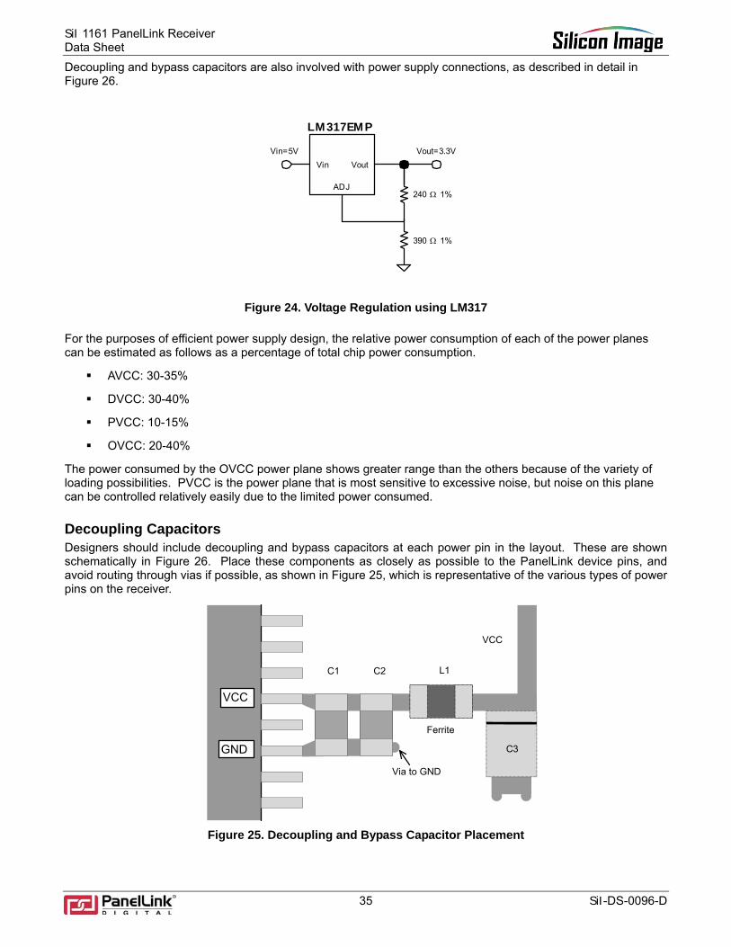
Decoupling and bypass capacitors are also involved with power supply connections, as described in detail in Figure 26.
Vin=5V Vout=3.3V
ADJ
Vin Vout
LM 317EM P
240 Ω 1%
390 Ω 1%
Figure 24. Voltage Regulation using LM317
For the purposes of efficient power supply design, the relative power consumption of each of the power planes can be estimated as follows as a percentage of total chip power consumption.
AVCC: 30-35%
DVCC: 30-40%
PVCC: 10-15%
OVCC: 20-40%
The power consumed by the OVCC power plane shows greater range than the others because of the variety of loading possibilities. PVCC is the power plane that is most sensitive to excessive noise, but noise on this plane can be controlled relatively easily due to the limited power consumed.
Decoupling Capacitors Designers should include decoupling and bypass capacitors at each power pin in the layout. These are shown schematically in Figure 26. Place these components as closely as possible to the PanelLink device pins, and avoid routing through vias if possible, as shown in Figure 25, which is representative of the various types of power pins on the receiver.
L1 C1
VCC
Ferrite
Via to GND
VCC
GND
C2
C3
Figure 25. Decoupling and Bypass Capacitor Placement
SiI 1161 PanelLink ReceiverData Sheet
SiI-DS-0096-D 36
VCCPIN
C1 C2
L1
C3
VCC
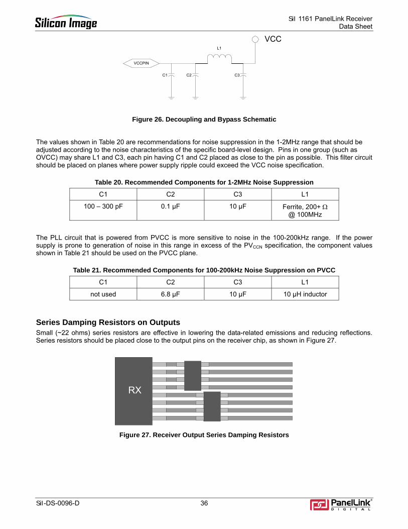
Figure 26. Decoupling and Bypass Schematic
The values shown in Table 20 are recommendations for noise suppression in the 1-2MHz range that should be adjusted according to the noise characteristics of the specific board-level design. Pins in one group (such as OVCC) may share L1 and C3, each pin having C1 and C2 placed as close to the pin as possible. This filter circuit should be placed on planes where power supply ripple could exceed the VCC noise specification.
Table 20. Recommended Components for 1-2MHz Noise Suppression
C1 C2 C3 L1
100 – 300 pF 0.1 µF 10 µF Ferrite, 200+ Ω @ 100MHz
The PLL circuit that is powered from PVCC is more sensitive to noise in the 100-200kHz range. If the power supply is prone to generation of noise in this range in excess of the PVCCN specification, the component values shown in Table 21 should be used on the PVCC plane.
Table 21. Recommended Components for 100-200kHz Noise Suppression on PVCC
C1 C2 C3 L1
not used 6.8 µF 10 µF 10 µH inductor
Series Damping Resistors on Outputs Small (~22 ohms) series resistors are effective in lowering the data-related emissions and reducing reflections. Series resistors should be placed close to the output pins on the receiver chip, as shown in Figure 27.
RX
Figure 27. Receiver Output Series Damping Resistors
SiI 1161 PanelLink Receiver Data Sheet
37 SiI-DS-0096-D
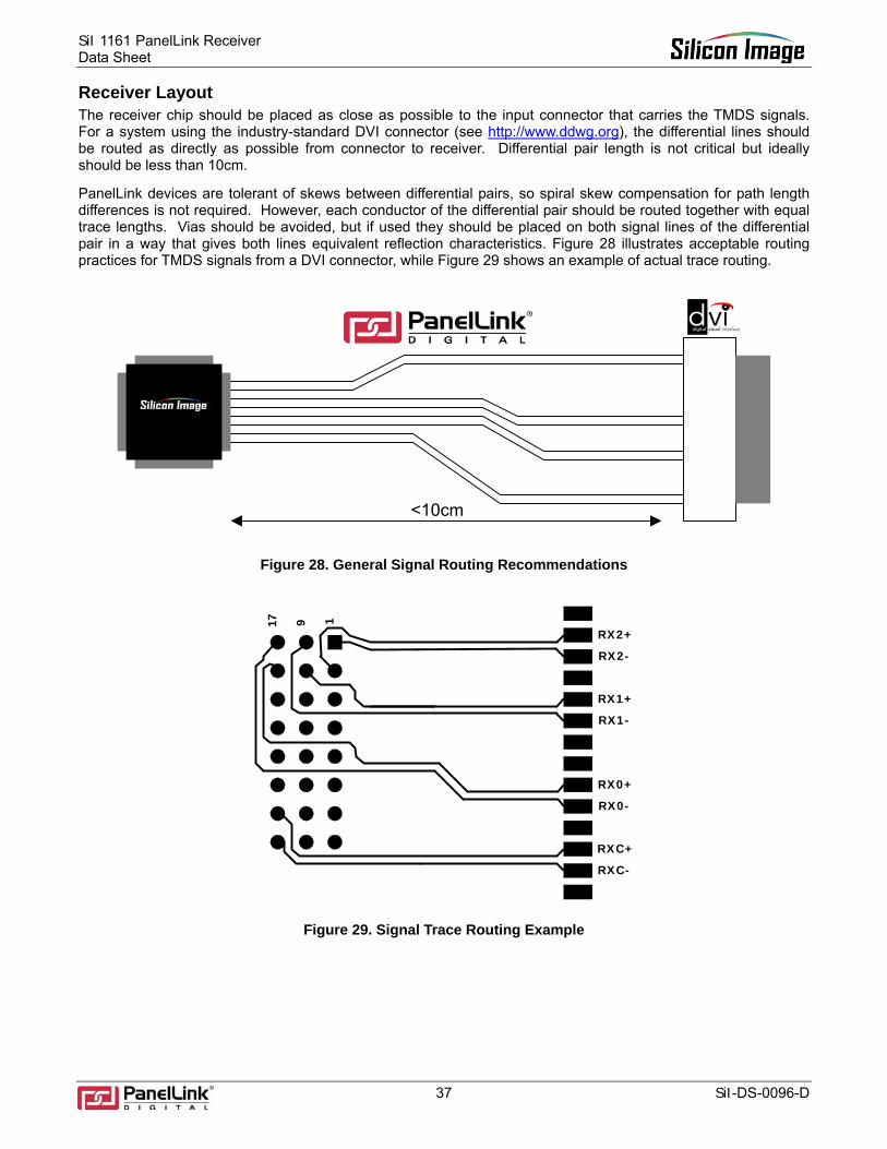
Receiver Layout The receiver chip should be placed as close as possible to the input connector that carries the TMDS signals. For a system using the industry-standard DVI connector (see http://www.ddwg.org), the differential lines should be routed as directly as possible from connector to receiver. Differential pair length is not critical but ideally should be less than 10cm.
PanelLink devices are tolerant of skews between differential pairs, so spiral skew compensation for path length differences is not required. However, each conductor of the differential pair should be routed together with equal trace lengths. Vias should be avoided, but if used they should be placed on both signal lines of the differential pair in a way that gives both lines equivalent reflection characteristics. Figure 28 illustrates acceptable routing practices for TMDS signals from a DVI connector, while Figure 29 shows an example of actual trace routing.
Figure 28. General Signal Routing Recommendations
RXC-
RXC+
RX0-
RX0+
RX1-
RX1+
RX2-
RX2+
1917
Figure 29. Signal Trace Routing Example
<10cm
SiI 1161 PanelLink ReceiverData Sheet
SiI-DS-0096-D 38
PCB Ground Planes All ground pins on the device should be connected to the same, contiguous ground plane in the PCB. This helps to avoid ground loops and inductances from one ground plane segment to another. Such low-inductance ground paths are critical for return currents, which affect EMI performance. The entire ground plane surrounding the PanelLink receiver should be one piece, and include the ground vias for the DVI connector.
As defined in the DVI 1.0 Specification, the impedance of the traces between the connector and the receiver should be 100Ω differentially, and close to 50Ω single-ended. The 100Ω requirement is to best match the differential impedance of the cable and connectors, to prevent reflections. The common mode currents are very small on the TMDS interface, so differential impedance is more important than single-ended.
Staggered Outputs and Two Pixels per Clock PanelLink receivers offer two features that can minimize the switching effects of the high-speed output data bus: two pixels per clock mode and staggered outputs.
The receiver can output one or two pixels in each output clock cycle. By widening the bus to two pixels per clock whenever possible, the clock speed is halved and the switching period of the data signals themselves is twice as long as in one pixel per clock mode. Typically, SXGA-resolution and above LCD panels expect to be connected with a 36-bit or 48-bit bus, two pixels per clock. Most XGA-resolution and below LCD panels use an 18- to 24-bit one pixel per clock interface.
When in two pixel per clock mode, the STAG_OUT# pin on receivers provides an additional means of reducing simultaneous switching activity. When enabled (STAG_OUT# = Low), only half of the output data pins switch together. The other half are switched one quarter clock cycle later. Note that both pixel buses use the same clock. Therefore, the staggered bus will have one quarter clock cycle less setup time to the clock, and one quarter clock cycle more hold time. Board designers driving into another clocked chip should take this into account in their timing analysis.
Silicon Image recommends the use of STAG_OUT# and the two pixels per clock mode whenever possible.
Adjusting Output Timings for Loading If not using the I2C drive strength programmability, the SiI 1161 can be made to accommodate different output loads by adding external capacitance. Refer to Figure 3 for an illustration of the loading requirements on DE and ODCK.
SiI 1161 PanelLink Receiver Data Sheet
39 SiI-DS-0096-D
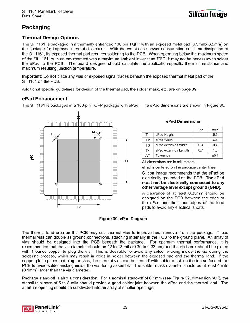
Packaging
Thermal Design Options The SiI 1161 is packaged in a thermally enhanced 100 pin TQFP with an exposed metal pad (6.5mmx 6.5mm) on the package for improved thermal dissipation. With the worst-case power consumption and heat dissipation of the SiI 1161, its exposed thermal pad requires soldering to the PCB. When operating below the maximum speed of the SiI 1161, or in an environment with a maximum ambient lower than 70ºC, it may not be necessary to solder the ePad to the PCB. The board designer should calculate the application-specific thermal resistance and maximum resulting junction temperature.
Important: Do not place any vias or exposed signal traces beneath the exposed thermal metal pad of the SiI 1161 on the PCB.
Additional specific guidelines for design of the thermal pad, the solder mask, etc. are on page 39.
ePad Enhancement The SiI 1161 is packaged in a 100-pin TQFP package with ePad. The ePad dimensions are shown in Figure 30.
T1
T2
C
C
T3 T4
ePad Dimensions
typ max
T1 ePad Height 6.5
T2 ePad Width 6.5
T3 ePad extension Width 0.3 0.4
T4 ePad extension Length 0.7 1.0
∆T Tolerance ±0.1
All dimensions are in millimeters. ePad is centered on the package center lines. Silicon Image recommends that the ePad be electrically grounded on the PCB. The ePad must not be electrically connected to any other voltage level except ground (GND). A clearance of at least 0.25mm should be designed on the PCB between the edge of the ePad and the inner edges of the lead pads to avoid any electrical shorts.
Figure 30. ePad Diagram
The thermal land area on the PCB may use thermal vias to improve heat removal from the package. These thermal vias can double as ground connections, attaching internally in the PCB to the ground plane. An array of vias should be designed into the PCB beneath the package. For optimum thermal performance, it is recommended that the via diameter should be 12 to 13 mils (0.30 to 0.33mm) and the via barrel should be plated with 1 ounce copper to plug the via. This is desirable to avoid any solder wicking inside the via during the soldering process, which may result in voids in solder between the exposed pad and the thermal land. If the copper plating does not plug the vias, the thermal vias can be ‘tented’ with solder mask on the top surface of the PCB to avoid solder wicking inside the via during assembly. The solder mask diameter should be at least 4 mils (0.1mm) larger than the via diameter.
Package stand-off is also a consideration. For a nominal stand-off of 0.1mm (see Figure 32, dimension ‘A1’), the stencil thickness of 5 to 8 mils should provide a good solder joint between the ePad and the thermal land. The aperture opening should be subdivided into an array of smaller openings.
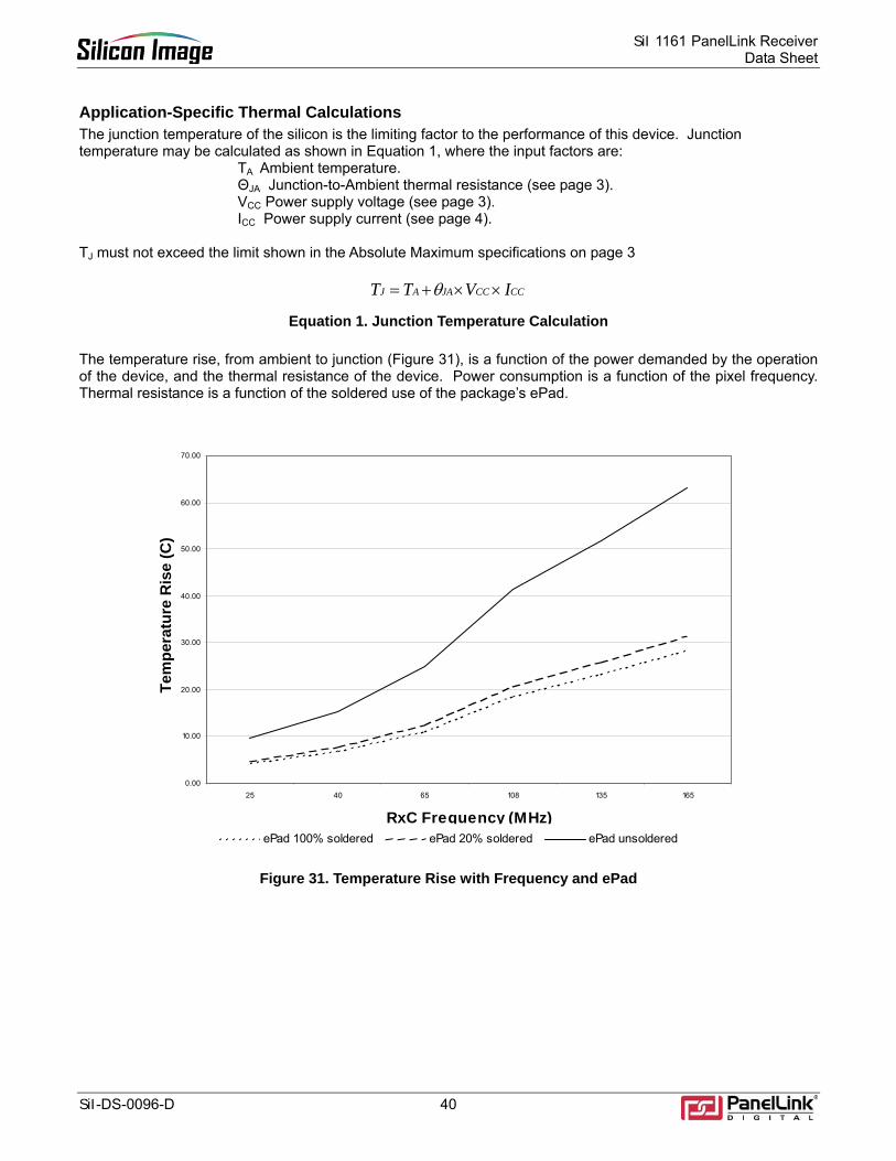
SiI 1161 PanelLink ReceiverData Sheet
SiI-DS-0096-D 40
Application-Specific Thermal Calculations The junction temperature of the silicon is the limiting factor to the performance of this device. Junction temperature may be calculated as shown in Equation 1, where the input factors are:
TA Ambient temperature. ΘJA Junction-to-Ambient thermal resistance (see page 3). VCC Power supply voltage (see page 3). ICC Power supply current (see page 4).
TJ must not exceed the limit shown in the Absolute Maximum specifications on page 3
CCCCJAAJ IVTT ××+= θ
Equation 1. Junction Temperature Calculation The temperature rise, from ambient to junction (Figure 31), is a function of the power demanded by the operation of the device, and the thermal resistance of the device. Power consumption is a function of the pixel frequency. Thermal resistance is a function of the soldered use of the package’s ePad.
0.00
10.00
20.00
30.00
40.00
50.00
60.00
70.00
25 40 65 108 135 165
RxC Frequency (MHz)
Tem
pera
ture
Ris
e (C
)
ePad 100% soldered ePad 20% soldered ePad unsoldered
Figure 31. Temperature Rise with Frequency and ePad
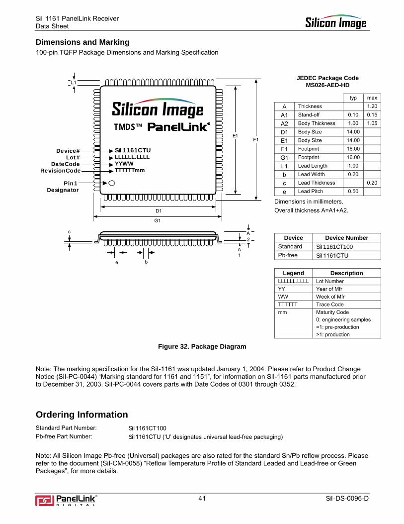
SiI 1161 PanelLink Receiver Data Sheet
41 SiI-DS-0096-D
Dimensions and Marking 100-pin TQFP Package Dimensions and Marking Specification
SiI1161CTULLLLLL.LLLLYYWWTTTTTTmm
Device #Lot #
Date CodeRevision Code
TMDS™E1
F1
D1
G1
A2
A1
L1
c
e b
Pin 1Designator
JEDEC Package Code MS026-AED-HD
typ max
A Thickness 1.20
A1 Stand-off 0.10 0.15
A2 Body Thickness 1.00 1.05
D1 Body Size 14.00
E1 Body Size 14.00
F1 Footprint 16.00
G1 Footprint 16.00
L1 Lead Length 1.00
b Lead Width 0.20
c Lead Thickness 0.20
e Lead Pitch 0.50
Dimensions in millimeters. Overall thickness A=A1+A2.
Device Device Number Standard SiI1161CT100 Pb-free SiI1161CTU
Legend Description
LLLLLL.LLLL Lot Number YY Year of Mfr WW Week of Mfr TTTTTT Trace Code mm Maturity Code
0: engineering samples =1: pre-production >1: production
Figure 32. Package Diagram
Note: The marking specification for the SiI-1161 was updated January 1, 2004. Please refer to Product Change Notice (SiI-PC-0044) “Marking standard for 1161 and 1151”, for information on SiI-1161 parts manufactured prior to December 31, 2003. SiI-PC-0044 covers parts with Date Codes of 0301 through 0352.
Ordering Information Standard Part Number: SiI1161CT100 Pb-free Part Number: SiI1161CTU (‘U’ designates universal lead-free packaging)
Note: All Silicon Image Pb-free (Universal) packages are also rated for the standard Sn/Pb reflow process. Please refer to the document (SiI-CM-0058) “Reflow Temperature Profile of Standard Leaded and Lead-free or Green Packages”, for more details.
SiI 1161 PanelLink ReceiverData Sheet
SiI-DS-0096-D 42
© 2004, 2005 Silicon Image. Inc.
Silicon Image, Inc. Tel: (408) 616-4000 1060 E. Arques Avenue Sunnyvale, CA 94085 USA
Fax: (408) 830-9530 E-mail: [email protected] Web: www.siliconimage.com