Embed Size (px)
Citation preview

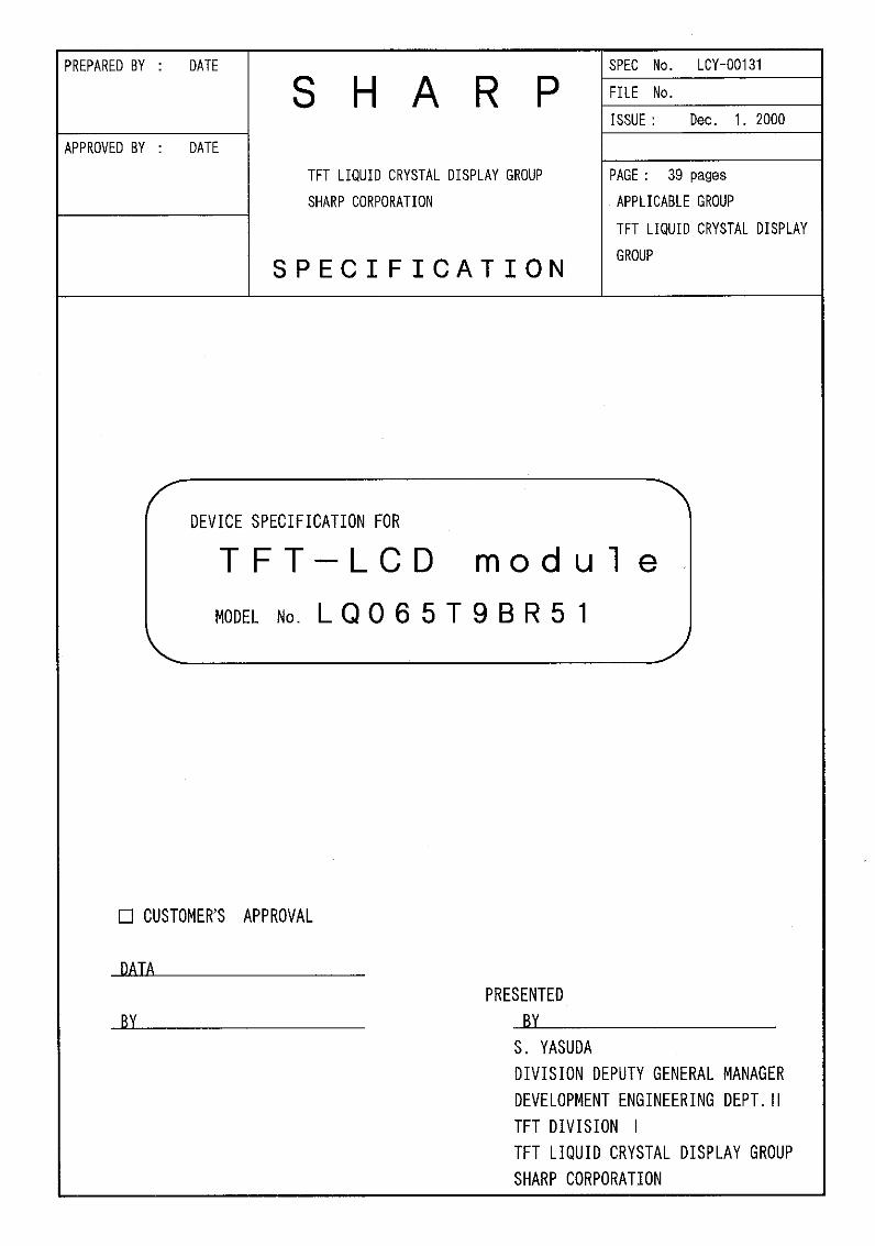
LQ065T9BR51 Color TFT LCD Module
(Model Number: LQ065T9BR51)
Specifications
Spec No.: LCY-00065 Dated: May 31. 2002
LCY00131-1
NOTICE This publication is the proprietary of SHARP and is copyrighted, with all rights reserved. Under the copyright laws, no part of this publication may be reproduced or transmitted in any form or by any means, electronic or mechanical for any purpose, in whole or in part, without the express written permission of SHARP. Express written permission is also required before any use of this publication may be made by a third party. The application circuit examples in this publication are provided to explain the representative applications of SHARP's devices and are not intended to guarantee any circuit design or permit any industrial property right or other rights to be executed. SHARP takes no responsibility for any problems related to any industrial property right or a third party resulting from the use of SHARP's devices, except for those resulting directly from device manufacturing processes. In the absence of confirmation by device specification sheets, SHARP takes no responsibility for any defects that occur in equipment using any of SHARP's devices, shown in catalogs, data books, etc. Contact SHARP in order to obtain the latest device specification sheets before using any SHARP's device. SHARP reserves the right to make changes in the specifications, characteristics, data, materials, structures and other contents described herein at any time without notice in order to improve design or reliability. Contact SHARP in order to obtain the latest specification sheets before using any SHARP's device. Manufacturing locations are also subject to change without notice. Observe the following points when using any device in this publication. SHARP takes no responsibility for damage caused by improper use of the devices. The devices in this publication are designed for use in general electronic equipment designs, such as: ・Personal computers ・Office automation ・Telecommunication equipment ・Test and measurement equipment ・Industrial control ・Audio visual and multimedia equipment ・Consumer electronics The appropriate design measures should be taken to ensure reliability and safety when SHARP's devices are used for equipment such as: ・Transportation control and safety equipment(i.e.,aircraft,trains,automobiles,etc.) ・Traffic signals ・Gas leakage sensor breakers ・Alarm equipment ・Various safety devices etc. SHARP's devices shall not be used for equipment that requires extremely high level of reliability, such as: ・Military and space applications ・Nuclear power control equipment ・Medical equipment for life support Contact a SHARP representative, in advance, when intending to use SHARP's devices for any "specific" applications other than those recommended by SHARP. Contact and consult with a SHARP representative if there are any questions about the contents of this publication.
LCY00131-2
C O N T E N T S
Page (1) Introduction ……………………………………… 3 (2) Features ……………………………………… 3 (3) Construction and Outline ……………………………………… 3 (4) Module geometry ……………………………………… 3 (5) Input/Output symbol and description ……………………………………… 4 (6) Absolute maximum ratings ……………………………………… 9 (7) Electrical characteristics ……………………………………… 10 (8) Optical characteristics ……………………………………… 15 (9) Mechanical characteristics ……………………………………… 18 (10) Display quality ……………………………………… 20 (11) Handling instruction ……………………………………… 20 (12) Shipping requirements ……………………………………… 22 (13) Reliability test items ……………………………………… 22 (14) Others ……………………………………… 22 Attached Figures Fig 1.Outline dimension of TFT-LCD module ………………… 24 Fig 2.Construction of TFT-LCD module ………………… 25 Fig 3.Packing form ………………… 26 Fig 4.Input/Output signal waveforms ………………… 27 Fig 5.Measurement method of optical characteristic (Transmissive mode)
………………… 36 Fig 6.Measurement method of optical characteristic (Reflective mode)
………………… 37 Attached sheet
(Appendix-1)Adjusting method of common electrode DC bias voltage ………………… 38
LCY00131-3
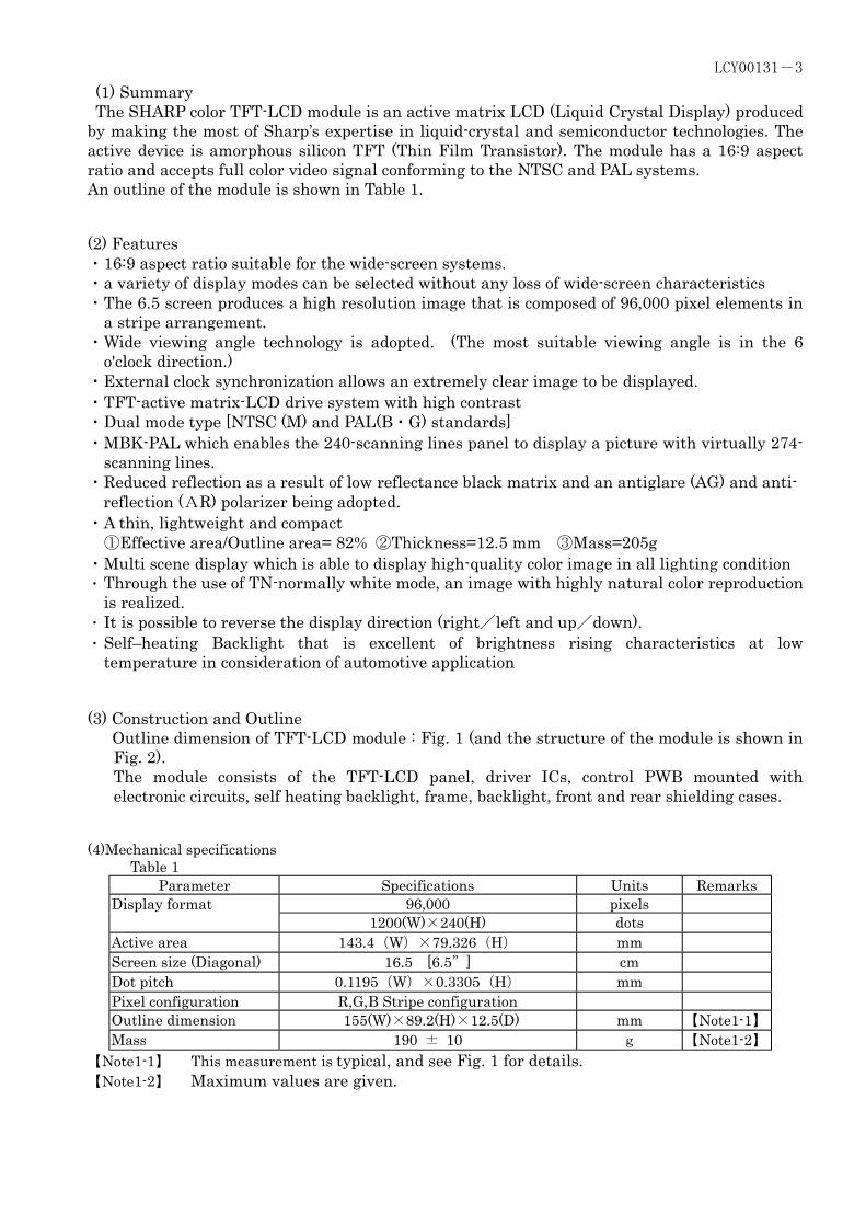
(1) Summary The SHARP color TFT-LCD module is an active matrix LCD (Liquid Crystal Display) produced by making the most of Sharp’s expertise in liquid-crystal and semiconductor technologies. The active device is amorphous silicon TFT (Thin Film Transistor). The module has a 16:9 aspect ratio and accepts full color video signal conforming to the NTSC and PAL systems. An outline of the module is shown in Table 1. (2) Features ・ 16:9 aspect ratio suitable for the wide-screen systems. ・ a variety of display modes can be selected without any loss of wide-screen characteristics ・ The 6.5 screen produces a high resolution image that is composed of 96,000 pixel elements in
a stripe arrangement. ・ Wide viewing angle technology is adopted. (The most suitable viewing angle is in the 6
o'clock direction.) ・External clock synchronization allows an extremely clear image to be displayed. ・ TFT-active matrix-LCD drive system with high contrast ・ Dual mode type [NTSC (M) and PAL(B・G) standards] ・ MBK-PAL which enables the 240-scanning lines panel to display a picture with virtually 274-
scanning lines. ・ Reduced reflection as a result of low reflectance black matrix and an antiglare (AG) and anti- reflection (AR) polarizer being adopted. ・ A thin, lightweight and compact
①Effective area/Outline area= 82% ②Thickness=12.5 mm ③Mass=205g ・ Multi scene display which is able to display high-quality color image in all lighting condition ・ Through the use of TN-normally white mode, an image with highly natural color reproduction
is realized. ・ It is possible to reverse the display direction (right/left and up/down). ・ Self–heating Backlight that is excellent of brightness rising characteristics at low
temperature in consideration of automotive application
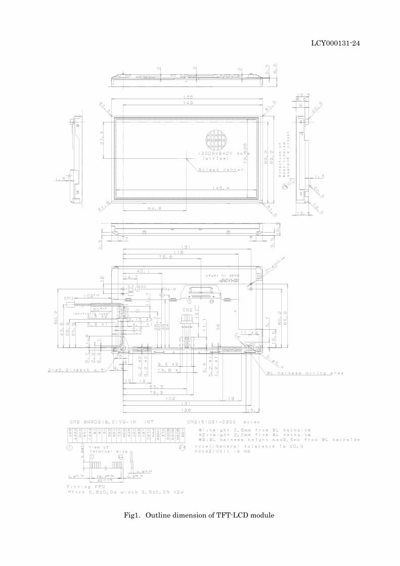
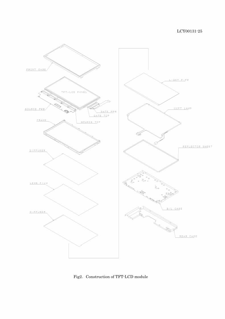
(3) Construction and Outline Outline dimension of TFT-LCD module : Fig. 1 (and the structure of the module is shown in
Fig. 2). The module consists of the TFT-LCD panel, driver ICs, control PWB mounted with electronic circuits, self heating backlight, frame, backlight, front and rear shielding cases.
(4)Mechanical specifications Table 1
Parameter Specifications Units Remarks 96,000 pixels Display format
1200(W)×240(H) dots Active area 143.4(W)×79.326(H) mm Screen size (Diagonal) 16.5 [6.5”] cm Dot pitch 0.1195(W)×0.3305(H) mm Pixel configuration R,G,B Stripe configuration Outline dimension 155(W)×89.2(H)×12.5(D) mm 【Note1-1】 Mass 190 ± 10 g 【Note1-2】
【Note1-1】 This measurement is typical, and see Fig. 1 for details. 【Note1-2】 Maximum values are given.
LCY00131-4
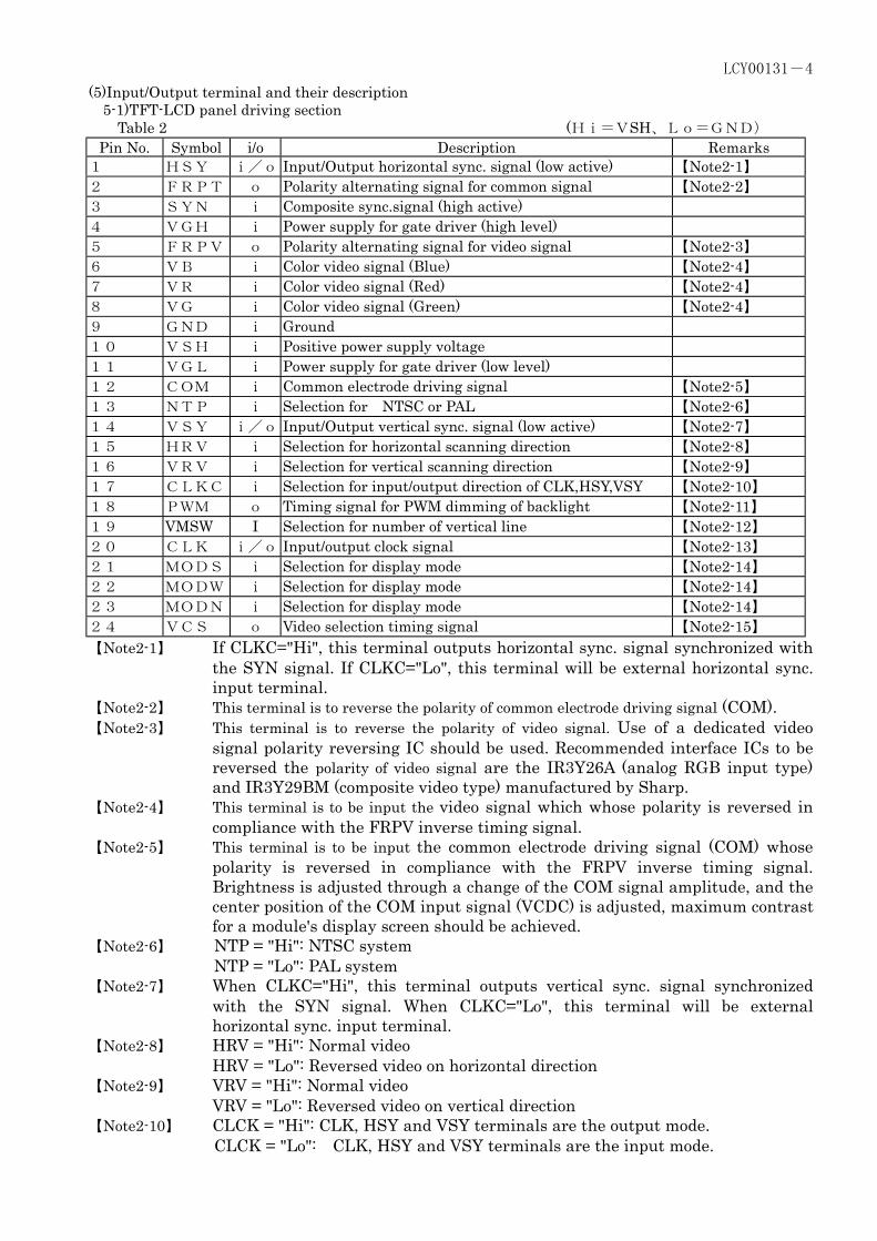
(5)Input/Output terminal and their description 5-1)TFT-LCD panel driving section Table 2 (Hi=VSH、Lo=GND)
Pin No. Symbol i/o Description Remarks 1 HSY i/o Input/Output horizontal sync. signal (low active) 【Note2-1】 2 FRPT o Polarity alternating signal for common signal 【Note2-2】 3 SYN i Composite sync.signal (high active) 4 VGH i Power supply for gate driver (high level) 5 FRPV o Polarity alternating signal for video signal 【Note2-3】 6 VB i Color video signal (Blue) 【Note2-4】 7 VR i Color video signal (Red) 【Note2-4】 8 VG i Color video signal (Green) 【Note2-4】 9 GND i Ground 10 VSH i Positive power supply voltage 11 VGL i Power supply for gate driver (low level) 12 COM i Common electrode driving signal 【Note2-5】 13 NTP i Selection for NTSC or PAL 【Note2-6】 14 VSY i/o Input/Output vertical sync. signal (low active) 【Note2-7】 15 HRV i Selection for horizontal scanning direction 【Note2-8】 16 VRV i Selection for vertical scanning direction 【Note2-9】 17 CLKC i Selection for input/output direction of CLK,HSY,VSY 【Note2-10】 18 PWM o Timing signal for PWM dimming of backlight 【Note2-11】 19 VMSW I Selection for number of vertical line 【Note2-12】 20 CLK i/o Input/output clock signal 【Note2-13】 21 MODS i Selection for display mode 【Note2-14】 22 MODW i Selection for display mode 【Note2-14】 23 MODN i Selection for display mode 【Note2-14】 24 VCS o Video selection timing signal 【Note2-15】 【Note2-1】 If CLKC="Hi", this terminal outputs horizontal sync. signal synchronized with
the SYN signal. If CLKC="Lo", this terminal will be external horizontal sync. input terminal.
【Note2-2】 This terminal is to reverse the polarity of common electrode driving signal (COM). 【Note2-3】 This terminal is to reverse the polarity of video signal. Use of a dedicated video
signal polarity reversing IC should be used. Recommended interface ICs to be reversed the polarity of video signal are the IR3Y26A (analog RGB input type) and IR3Y29BM (composite video type) manufactured by Sharp.
【Note2-4】 This terminal is to be input the video signal which whose polarity is reversed in compliance with the FRPV inverse timing signal.
【Note2-5】 This terminal is to be input the common electrode driving signal (COM) whose polarity is reversed in compliance with the FRPV inverse timing signal. Brightness is adjusted through a change of the COM signal amplitude, and the center position of the COM input signal (VCDC) is adjusted, maximum contrast for a module's display screen should be achieved.
【Note2-6】 NTP = "Hi": NTSC system NTP = "Lo": PAL system
【Note2-7】 When CLKC="Hi", this terminal outputs vertical sync. signal synchronized with the SYN signal. When CLKC="Lo", this terminal will be external horizontal sync. input terminal.
【Note2-8】 HRV = "Hi": Normal video HRV = "Lo": Reversed video on horizontal direction
【Note2-9】 VRV = "Hi": Normal video VRV = "Lo": Reversed video on vertical direction
【Note2-10】 CLCK = "Hi": CLK, HSY and VSY terminals are the output mode. CLCK = "Lo": CLK, HSY and VSY terminals are the input mode.
LCY00131-5
【Note2-11】 PWM signal is used for the PWM dimming frequency and it is possible to control the PWM signal dimming by combining both HSY and PWM signal. But, please use this PWM signal just in case of inputting standard NTSC or PAL signal. (See Fig.4-I)
【Note2-12】 VMSW = “Hi”: Vertical 240 line display VMSW = ‘Lo”: Vertical 234 line display Masking signal for upper 1 line and bottom 5 line is output with VCS signal.
【Note2-13】 When CLKC="Hi", this terminal outputs low level. When CLKC="Lo", this terminal will be external clock input terminal. This signal should correspond to sampling timing of the horizontal direction image. NTP, MODS, MODW, and MODN should be "Hi" when CLKC="Lo".
【Note2-14】 Display mode settings are shown in Table 3. 【Note2-15】 In case of normal mode (MODS="Hi", MODW="Lo", MODN="Hi"), it is possible
to get an excellent display by masking of video signal based on the VCS output signal. The video signal is masked when VCS is "Hi" (the two edges of the screen). (In case of black masking display, it is possible to easily get the normal screen (full frame) by inputting the VCS signal at the system switching terminal of the video interface IC, inputting the field signal into another video input and inputting a signal for black into the other video input. And also, in case of vertical 234 lines, the masking signal of upper 1 line and bottom 5 lines is output regardless of display mode. In case of the other condition except above, the output of VCS becomes “Lo”. In case of the module test mode, the test signal is output.
LCY00131-6
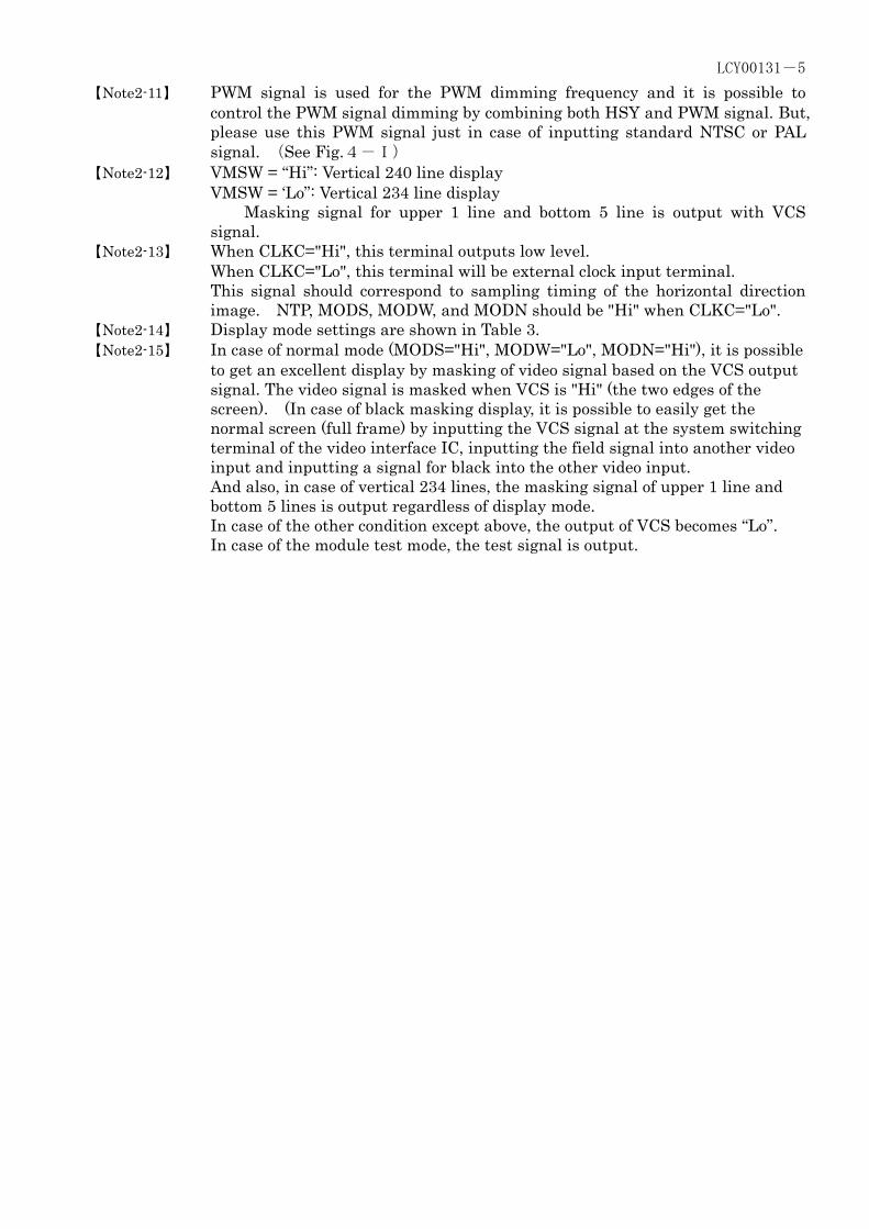
Table 3 Display Method and Characteristics MODS MODW MODN Display
mode Characteristics Source example
H H H Full mode
The picture is displayed with uniform enlargement in the horizontal direction, and the horizontal retrace line of the input signal cannot be seen. If the video sampling frequency of the image is fixed and a 4:3 video signal is displayed, the picture will be prominently oblong.
4:3 signal, Navigationsignal
Fig.3-1
H H L Wide 1 mode
A 4:3 video signal is displayed with less feeling of incongruity than that in the full screen mode. Since the video horizontal sampling frequency is modulated in the horizontal direction, the degree of perfect roundness in the center of the screen is improved over that of the full screen mode.
4:3 signal Fig.3-2
H L H Normal mode
When displaying a 4:3 video signal, the displayed image is slightly less than perfectly round and the horizontal retrace line period is displayed at the two edges of the screen. With respect to the video horizontal sampling frequency, the center portion of the screen is slightly lower and the two edges become slightly higher. With respect to the horizontal retrace line period, a far better display is achieved than that of masking of the video signal by the VCS signal timing.
4:3 signal Fig.3-3
H L L Cinema mode
A letter-box type image (16:9 signal) is displayed over the central width of the screen. In the horizontal direction, full screen display is utilized. Due to the display being extended in the vertical direction, a slightly less than perfectly round image is displayed.
letter box type wide signal(16:9signal)
Fig.3-4
L H H Wide 2 mode
In the horizontal direction, the Wide 1 display mode is employed. Due to the display being extended in the vertical direction, the portion of the picture in the center of the screen is slightly less than perfectly round. Also due to extending in the vertical direction, the upper and lower potions of the image are not displayed.
4:3 signal Fig.3-5
L H L test This mode is unusable as it is the test mode. - - L L H test This mode is unusable as it is the test mode. - - L L L test This mode is unusable as it is the test mode. - -
LCY00131-7
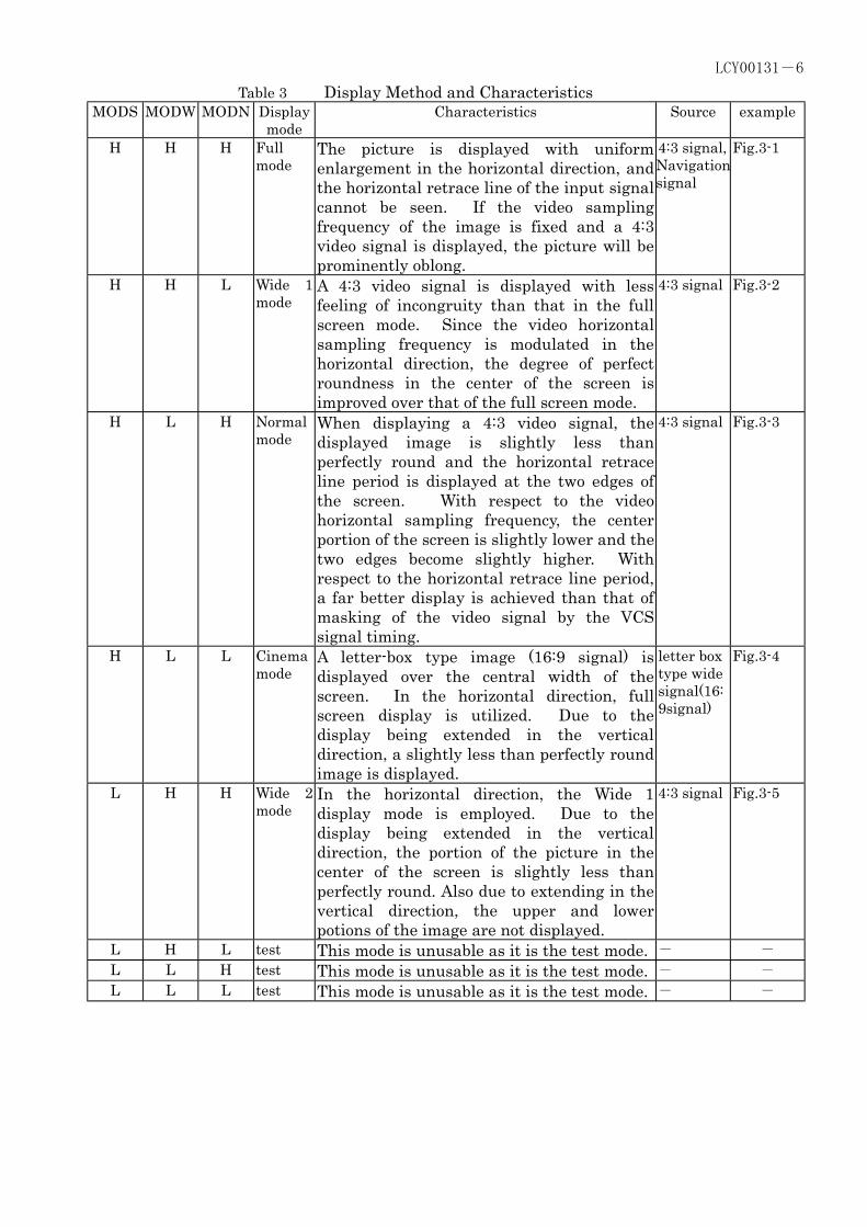
Fig.3-5 Wide 2 mode
Fig.3-4 Cinema mode
Fig.3-3 Normal mode
Fig.3-2 Wide 1 mode
Fig.3-1 Full mode
LCY00131-8
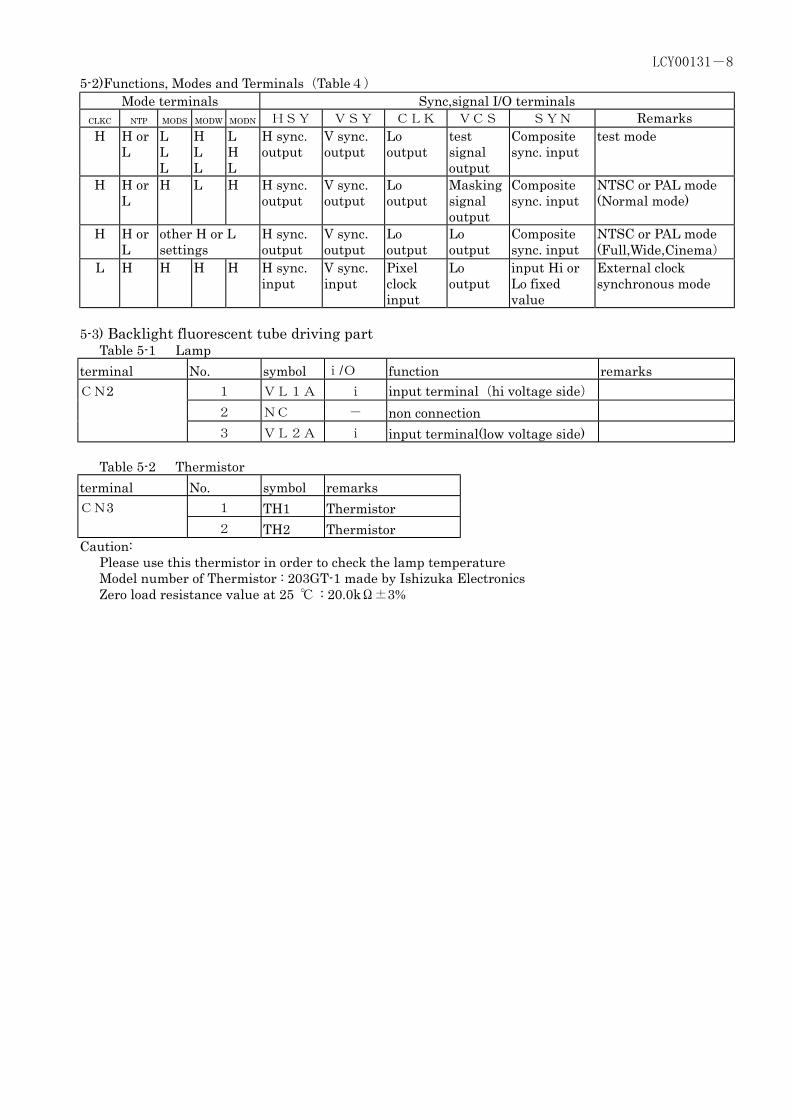
5-2)Functions, Modes and Terminals(Table4) Mode terminals Sync,signal I/O terminals
CLKC NTP MODS MODW MODN HSY VSY CLK VCS SYN Remarks H H or
L L L L
H L L
L H L
H sync. output
V sync. output
Lo output
test signal output
Composite sync. input
test mode
H H or L
H L H H sync. output
V sync. output
Lo output
Masking signal output
Composite sync. input
NTSC or PAL mode (Normal mode)
H H or L
other H or L settings
H sync. output
V sync. output
Lo output
Lo output
Composite sync. input
NTSC or PAL mode (Full,Wide,Cinema)
L H H H H H sync. input
V sync. input
Pixel clock input
Lo output
input Hi or Lo fixed value
External clock synchronous mode
5-3) Backlight fluorescent tube driving part Table 5-1 Lamp terminal No. symbol i/O function remarks CN2 1 VL1A i input terminal(hi voltage side) 2 NC - non connection 3 VL2A i input terminal(low voltage side) Table 5-2 Thermistor terminal No. symbol remarks CN3 1 TH1 Thermistor 2 TH2 Thermistor Caution: Please use this thermistor in order to check the lamp temperature Model number of Thermistor : 203GT-1 made by Ishizuka Electronics Zero load resistance value at 25 ℃ : 20.0kΩ±3%
LCY00131-9
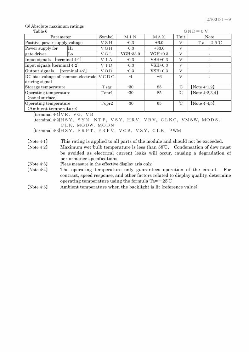
(6) Absolute maximum ratings Table 6 GND=0V
Parameter Symbol MIN MAX Unit Note Positive power supply voltage VSH -0.3 +6.0 V Ta=25℃ Power supply for Hi VGH -0.3 +33.0 V 〃 gate driver Lo VGL VGH-33.0 VGH+0.3 V 〃 Input signals [terminal 4-1] VIA -0.3 VSH+0.3 V 〃 Input signals [terminal 4-2] VID -0.3 VSH+0.3 V 〃 Output signals [terminal 4-3] VOD -0.3 VSH+0.3 V 〃 DC bias voltage of common electrode driving signal
VCDC -4 +6 V 〃
Storage temperature Tstg -30 85 ℃ 【Note 4-1,2】 Operating temperature (panel surface)
Topr1 -30 85 ℃ 【Note 4-2,3,4】
Operating temperature (Ambient temperature)
Topr2 -30 65 ℃ 【Note 4-4,5】
[terminal 4-1]VR,VG,VB [terminal 4-2]HSY,SYN,NTP,VSY,HRV,VRV,CLKC,VMSW,MODS, CLK,MODW,MODN [terminal 4-3]HSY,FRPT,FRPV,VCS,VSY,CLK,PWM 【Note 4-1】 This rating is applied to all parts of the module and should not be exceeded. 【Note 4-2】 Maximum wet-bulb temperature is less than 58℃. Condensation of dew must
be avoided as electrical current leaks will occur, causing a degradation of performance specifications.
【Note 4-3】 Pleas measure in the effective display aria only. 【Note 4-4】 The operating temperature only guarantees operation of the circuit. For
contrast, speed response, and other factors related to display quality, determine operating temperature using the formula Ta=+25℃
【Note 4-5】 Ambient temperature when the backlight is lit (reference value).
LCY00131-10
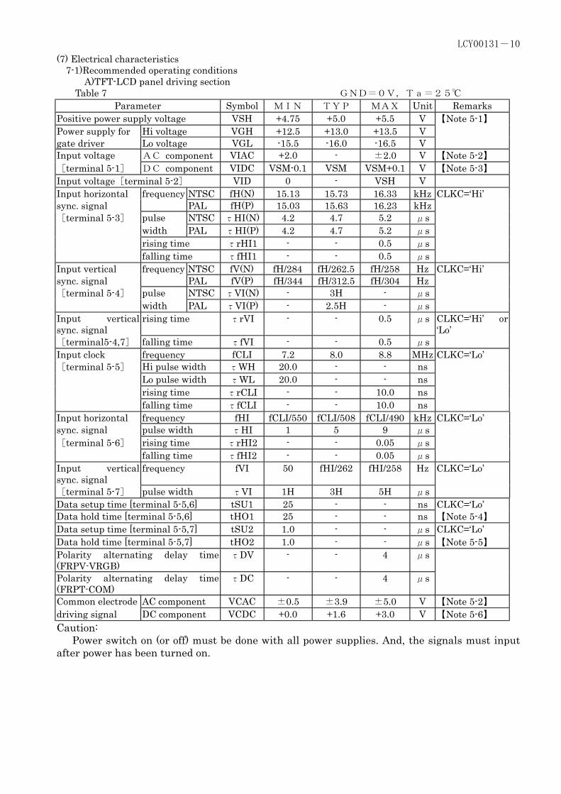
(7) Electrical characteristics 7-1)Recommended operating conditions A)TFT-LCD panel driving section Table 7 GND=0V,Ta=25℃
Parameter Symbol MIN TYP MAX Unit Remarks Positive power supply voltage VSH +4.75 +5.0 +5.5 V 【Note 5-1】 Power supply for Hi voltage VGH +12.5 +13.0 +13.5 V gate driver Lo voltage VGL -15.5 -16.0 -16.5 V Input voltage AC component VIAC +2.0 - ±2.0 V 【Note 5-2】 [terminal 5-1] DC component VIDC VSM-0.1 VSM VSM+0.1 V 【Note 5-3】 Input voltage[terminal 5-2] VID 0 - VSH V Input horizontal frequency NTSC fH(N) 15.13 15.73 16.33 kHz CLKC=‘Hi’ sync. signal PAL fH(P) 15.03 15.63 16.23 kHz [terminal 5-3] pulse NTSC τHI(N) 4.2 4.7 5.2 μs width PAL τHI(P) 4.2 4.7 5.2 μs rising time τrHI1 - - 0.5 μs falling time τfHI1 - - 0.5 μs Input vertical frequency NTSC fV(N) fH/284 fH/262.5 fH/258 Hz CLKC=‘Hi’ sync. signal PAL fV(P) fH/344 fH/312.5 fH/304 Hz [terminal 5-4] pulse NTSC τVI(N) - 3H - μs width PAL τVI(P) - 2.5H - μs Input vertical sync. signal
rising time τrVI - - 0.5 μs CLKC=‘Hi’ or ‘Lo’
[terminal5-4,7] falling time τfVI - - 0.5 μs Input clock frequency fCLI 7.2 8.0 8.8 MHz CLKC=‘Lo’ [terminal 5-5] Hi pulse width τWH 20.0 - - ns Lo pulse width τWL 20.0 - - ns rising time τrCLI - - 10.0 ns falling time τfCLI - - 10.0 ns Input horizontal frequency fHI fCLI/550 fCLI/508 fCLI/490 kHz CLKC=‘Lo’ sync. signal pulse width τHI 1 5 9 μs [terminal 5-6] rising time τrHI2 - - 0.05 μs falling time τfHI2 - - 0.05 μs Input vertical sync. signal
frequency fVI 50 fHI/262 fHI/258 Hz CLKC=‘Lo’
[terminal 5-7] pulse width τVI 1H 3H 5H μs Data setup time [terminal 5-5,6] tSU1 25 - - ns CLKC=‘Lo’ Data hold time [terminal 5-5,6] tHO1 25 - - ns 【Note 5-4】 Data setup time [terminal 5-5,7] tSU2 1.0 - - μs CLKC=‘Lo’ Data hold time [terminal 5-5,7] tHO2 1.0 - - μs 【Note 5-5】 Polarity alternating delay time (FRPV-VRGB)
τDV - - 4 μs
Polarity alternating delay time (FRPT-COM)
τDC - - 4 μs
Common electrode AC component VCAC ±0.5 ±3.9 ±5.0 V 【Note 5-2】 driving signal DC component VCDC +0.0 +1.6 +3.0 V 【Note 5-6】 Caution: Power switch on (or off) must be done with all power supplies. And, the signals must input after power has been turned on.
LCY00131-11
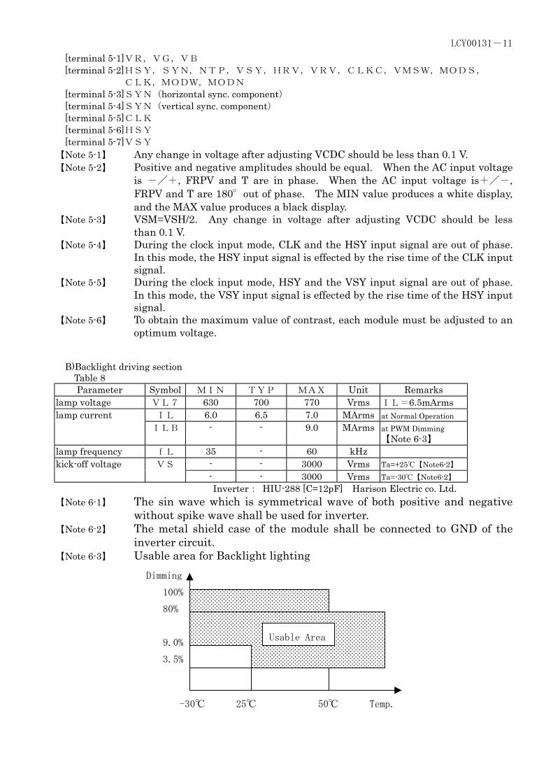
[terminal 5-1]VR,VG,VB [terminal 5-2]HSY,SYN,NTP,VSY,HRV,VRV,CLKC,VMSW,MODS, CLK,MODW,MODN
[terminal 5-3]SYN(horizontal sync. component) [terminal 5-4]SYN(vertical sync. component) [terminal 5-5]CLK [terminal 5-6]HSY [terminal 5-7]VSY 【Note 5-1】 Any change in voltage after adjusting VCDC should be less than 0.1 V. 【Note 5-2】 Positive and negative amplitudes should be equal. When the AC input voltage
is -/+, FRPV and T are in phase. When the AC input voltage is+/-, FRPV and T are 180°out of phase. The MIN value produces a white display, and the MAX value produces a black display.
【Note 5-3】 VSM=VSH/2. Any change in voltage after adjusting VCDC should be less than 0.1 V.
【Note 5-4】 During the clock input mode, CLK and the HSY input signal are out of phase. In this mode, the HSY input signal is effected by the rise time of the CLK input signal.
【Note 5-5】 During the clock input mode, HSY and the VSY input signal are out of phase. In this mode, the VSY input signal is effected by the rise time of the HSY input signal.
【Note 5-6】 To obtain the maximum value of contrast, each module must be adjusted to an optimum voltage.
B)Backlight driving section Table 8
Parameter Symbol MIN TYP MAX Unit Remarks lamp voltage VL7 630 700 770 Vrms IL=6.5mArms lamp current IL 6.0 6.5 7.0 MArms at Normal Operation ILB - - 9.0 MArms at PWM Dimming
【Note 6-3】 lamp frequency fL 35 - 60 kHz kick-off voltage VS - - 3000 Vrms Ta=+25℃【Note6-2】 - - 3000 Vrms Ta=-30℃【Note6-2】 Inverter: HIU-288 [C=12pF] Harison Electric co. Ltd. 【Note 6-1】 The sin wave which is symmetrical wave of both positive and negative
without spike wave shall be used for inverter. 【Note 6-2】 The metal shield case of the module shall be connected to GND of the
inverter circuit. 【Note 6-3】 Usable area for Backlight lighting
100%
80%
9.0%
3.5%
-30℃ 25℃
Dimming
Usable Area
50℃ Temp.
LCY00131-12
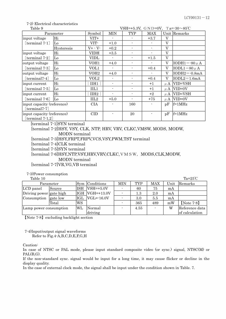
7-2) Electrical characteristics Table 9 VSH=+5.3V, GND=0V,Ta=-30~85℃
Parameter Symbol MIN TYP MAX Unit Remarks input voltage Hi VIT+ - - +3.7 V [terminal 7-1] Lo VIT- +1.0 - - V Hysteresis V+ - V- +0.2 - - V input voltage Hi VIDH +3.5 - - V [terminal 7-2] Lo VIDL - - +1.5 V output voltage Hi VOH1 +4.0 - - V IODH1=-80μA [terminal 7-3] Lo VOL1 - - +0.4 V IODL1=80μA output voltage Hi VOH2 +4.0 - - V IODH2=-0.8mA [terminal7-4] Lo VOL2 - - +0.4 V IODL2=1.6mA input current Hi |IIH1| - - +1 μA VID=VSH [terminal 7-5] Lo IIL1 - - +1 μA VID=0V input current Hi |IIH2| - - +2 μA VID=VSH [terminal 7-6] Lo IIL2 +5.0 - +75 μA VID=0V input capacity (reference) [terminal7-7]
CIA - 160 - pF f=1MHz
input capacity (reference) [terminal 7-1,2]
CID - 20 - pF f=1MHz
[terminal 7-1]SYN terminal [terminal 7-2]HSY, VSY, CLK, NTP, HRV, VRV, CLKC,VMSW, MODS, MODW, MODN terminal [terminal 7-3]HSY,FRPT,FRPV,VCS,VSY,PWM,TST terminal [terminal 7-4]CLK terminal [terminal 7-5]SYN terminal [terminal 7-6]HSY,NTP,VSY,HRV,VRV,CLKC,VMSW,MODS,CLK,MODW, MODN terminal [terminal 7-7]VR,VG,VB terminal 7-3)Power consumption Table 10 Ta=25℃
Parameter Sym Conditions MIN TYP MAX Unit Remarks LCD panel Source ISH VSH=+5.0V - 60 75 mA Driving power gate high IGH VGH=+13.0V - 1.3 2.0 mA Consumption gate low IGL VGL=-16.0V - 3.0 5.5 mA Total WS - 365 489 mW 【Note 7-8】 Lamp power consumption WL Normal
driving - 4.55 - W Reference data
of calculation 【Note 7-8】excluding backlight section 7-4)Input/output signal waveforms Refer to Fig.4-A,B,C,D,E,F,G,H Caution: In case of NTSC or PAL mode, please input standard composite video (or sync.) signal, NTSC(M) or PAL(B,G). If the non-standard sync. signal would be input for a long time, it may cause flicker or decline in the display quality. In the case of external clock mode, the signal shall be input under the condition shown in Table. 7.
LCY00131-13
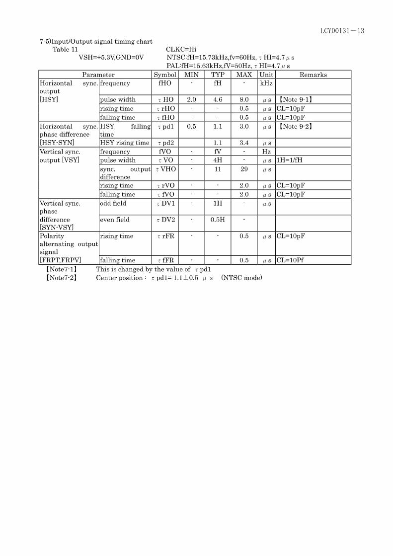
7-5)Input/Output signal timing chart Table 11 CLKC=Hi VSH=+5.3V,GND=0V NTSC:fH=15.73kHz,fv=60Hz,τHI=4.7μs PAL:fH=15.63kHz,fV=50Hz,τHI=4.7μs
Parameter Symbol MIN TYP MAX Unit Remarks Horizontal sync. output
frequency fHO - fH - kHz
[HSY] pulse width τHO 2.0 4.6 8.0 μs 【Note 9-1】 rising time τrHO - - 0.5 μs CL=10pF falling time τfHO - - 0.5 μs CL=10pF Horizontal sync. phase difference
HSY falling time
τpd1 0.5 1.1 3.0 μs 【Note 9-2】
[HSY-SYN] HSY rising time τpd2 1.1 3.4 μs Vertical sync. frequency fVO - fV - Hz output [VSY] pulse width τVO - 4H - μs 1H=1/fH sync. output
difference τVHO - 11 29 μs
rising time τrVO - - 2.0 μs CL=10pF falling time τfVO - - 2.0 μs CL=10pF Vertical sync. phase
odd field τDV1 - 1H - μs
difference [SYN-VSY]
even field τDV2 - 0.5H -
Polarity alternating output signal
rising time τrFR - - 0.5 μs CL=10pF
[FRPT,FRPV] falling time τfFR - - 0.5 μs CL=10Pf 【Note7-1】 This is changed by the value of τpd1 【Note7-2】 Center position : τpd1= 1.1±0.5 μs (NTSC mode)
LCY00131-14
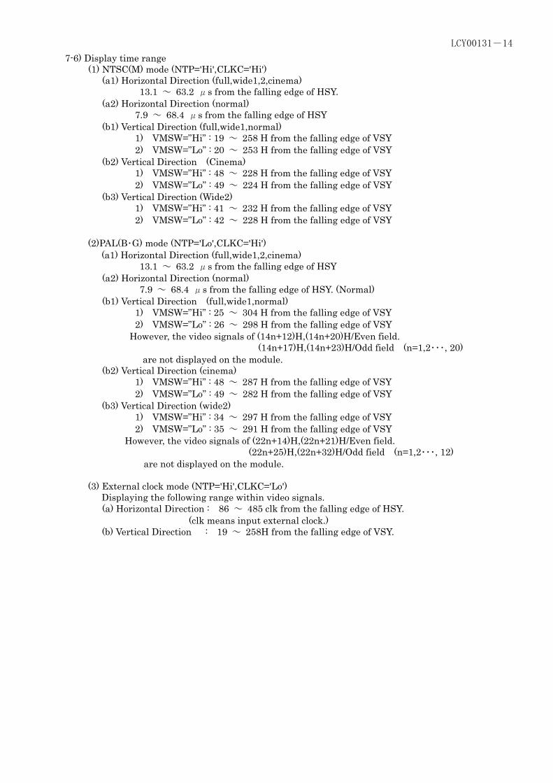
7-6) Display time range (1) NTSC(M) mode (NTP='Hi',CLKC='Hi') (a1) Horizontal Direction (full,wide1,2,cinema) 13.1 ~ 63.2 μs from the falling edge of HSY. (a2) Horizontal Direction (normal) 7.9 ~ 68.4 μs from the falling edge of HSY (b1) Vertical Direction (full,wide1,normal) 1) VMSW=”Hi” : 19 ~ 258 H from the falling edge of VSY 2) VMSW=”Lo” : 20 ~ 253 H from the falling edge of VSY (b2) Vertical Direction (Cinema) 1) VMSW=”Hi” : 48 ~ 228 H from the falling edge of VSY 2) VMSW=”Lo” : 49 ~ 224 H from the falling edge of VSY (b3) Vertical Direction (Wide2) 1) VMSW=”Hi” : 41 ~ 232 H from the falling edge of VSY 2) VMSW=”Lo” : 42 ~ 228 H from the falling edge of VSY (2)PAL(B・G) mode (NTP='Lo',CLKC='Hi') (a1) Horizontal Direction (full,wide1,2,cinema) 13.1 ~ 63.2 μs from the falling edge of HSY (a2) Horizontal Direction (normal) 7.9 ~ 68.4 μs from the falling edge of HSY. (Normal) (b1) Vertical Direction (full,wide1,normal) 1) VMSW=”Hi” : 25 ~ 304 H from the falling edge of VSY 2) VMSW=”Lo” : 26 ~ 298 H from the falling edge of VSY However, the video signals of (14n+12)H,(14n+20)H/Even field. (14n+17)H,(14n+23)H/Odd field (n=1,2・・・, 20) are not displayed on the module. (b2) Vertical Direction (cinema) 1) VMSW=”Hi” : 48 ~ 287 H from the falling edge of VSY 2) VMSW=”Lo” : 49 ~ 282 H from the falling edge of VSY (b3) Vertical Direction (wide2) 1) VMSW=”Hi” : 34 ~ 297 H from the falling edge of VSY 2) VMSW=”Lo” : 35 ~ 291 H from the falling edge of VSY However, the video signals of (22n+14)H,(22n+21)H/Even field. (22n+25)H,(22n+32)H/Odd field (n=1,2・・・, 12) are not displayed on the module. (3) External clock mode (NTP='Hi',CLKC='Lo') Displaying the following range within video signals. (a) Horizontal Direction : 86 ~ 485 clk from the falling edge of HSY. (clk means input external clock.) (b) Vertical Direction : 19 ~ 258H from the falling edge of VSY.
LCY00131-15
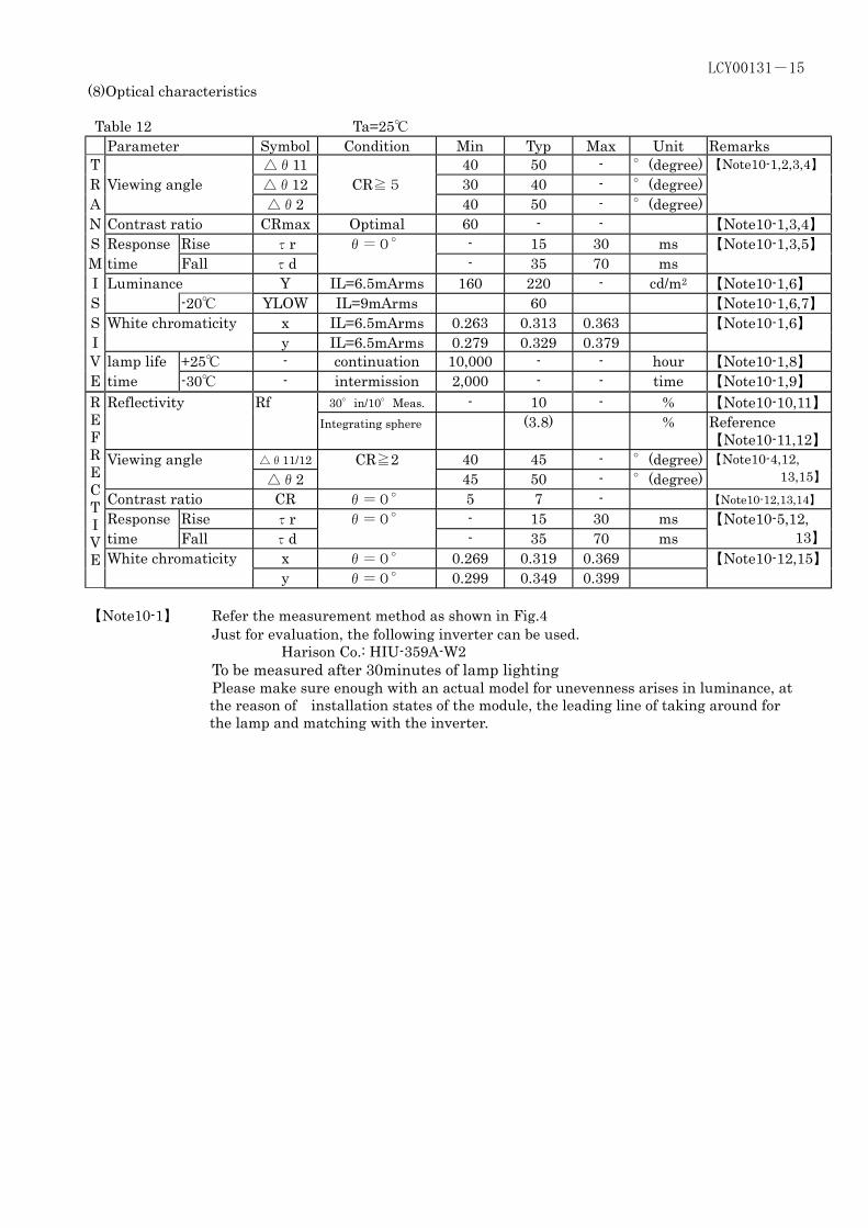
(8)Optical characteristics Table 12 Ta=25℃ Parameter Symbol Condition Min Typ Max Unit Remarks
T △θ11 40 50 - °(degree) 【Note10-1,2,3,4】 R Viewing angle △θ12 CR≧5 30 40 - °(degree) A △θ2 40 50 - °(degree) N Contrast ratio CRmax Optimal 60 - - 【Note10-1,3,4】 S Response Rise τr θ=0° - 15 30 ms 【Note10-1,3,5】 M time Fall τd - 35 70 ms I Luminance Y IL=6.5mArms 160 220 - cd/m2 【Note10-1,6】 S -20℃ YLOW IL=9mArms 60 【Note10-1,6,7】 S White chromaticity x IL=6.5mArms 0.263 0.313 0.363 【Note10-1,6】 I y IL=6.5mArms 0.279 0.329 0.379 V lamp life +25℃ - continuation 10,000 - - hour 【Note10-1,8】 E time -30℃ - intermission 2,000 - - time 【Note10-1,9】
Reflectivity Rf 30°in/10°Meas. - 10 - % 【Note10-10,11】 Integrating sphere (3.8) % Reference
【Note10-11,12】 Viewing angle △θ11/12 CR≧2 40 45 - °(degree) △θ2 45 50 - °(degree)
【Note10-4,12, 13,15】
Contrast ratio CR θ=0° 5 7 - 【Note10-12,13,14】 Response Rise τr θ=0° - 15 30 ms time Fall τd - 35 70 ms
【Note10-5,12, 13】
White chromaticity x θ=0° 0.269 0.319 0.369 【Note10-12,15】
R E F R E C T I V E
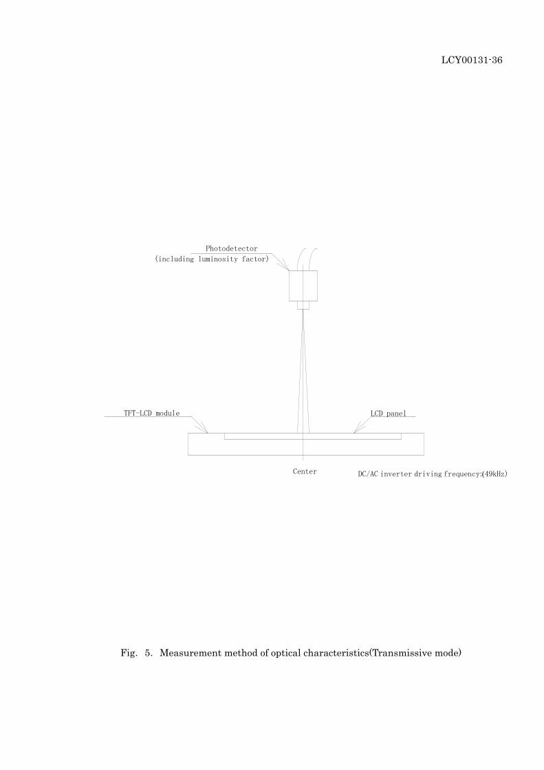
y θ=0° 0.299 0.349 0.399 【Note10-1】 Refer the measurement method as shown in Fig.4 Just for evaluation, the following inverter can be used. Harison Co.: HIU-359A-W2 To be measured after 30minutes of lamp lighting Please make sure enough with an actual model for unevenness arises in luminance, at the reason of installation states of the module, the leading line of taking around for the lamp and matching with the inverter.

LCY00131-16
【Note 10-2】 Viewing angle range is defined as follows.
6 o’clock direction
Normal line
θ2
θ2 θ12 θ11
definition for viewing angle 【Note 10-3】 Applied voltage condition for the measurement of transmissive mode: 1) VCDC is adjusted so as to attain maximum contrast ratio. 2) Input ±1.90V at VIAC. When VI50= transmission is 50% at Voltage-Transmission curve, Black level : Vi50=±2.5V, White level :Vi50 =+ 1.5V 【Note 10-4】 Contrast ratio is defined as follows: Photodetector output with LCD being "white" Contrast ratio(CR) = Photodetechor output with LCD being "black" 【Note 10-5】 Response time is obtained by measuring the transition time of photodetector
output, when input signals are applied so as to make the area "black" to and from "white".
0% 10%
90% 100%
Black White White
τd τr Time
Photodetecter output
(arbitrary unit)
LCY00131-17
【Note 10-6】 Measured on the center area of the panel at a viewing cone 1° by TOPCON luminance meter BM-7.(After 30 minutes operation) DC/AC inverter driving frequency:( 49kHz) 【Note 10-7】 Ambient temperature : -20℃ Measured luminance on the panel after 2 minutes operation. 【Note 10-8】 Lamp life time is defined as the time when either or occurs in the continuous operation under the condition of lamp current IL=3.0~7.0mArms and (Lighting Condition)
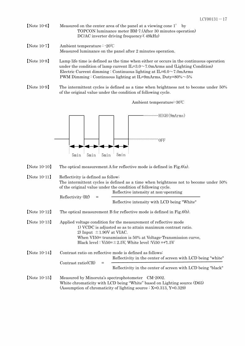
Electric Current dimming : Continuous lighting at IL=6.0~7.0mArms PWM Dimming : Continuous lighting at IL=9mArms, Duty=80%~5% 【Note 10-9】 The intermittent cycles is defined as a time when brightness not to become under 50%
of the original value under the condition of following cycle.
Ambient temperature:-30℃ 【Note 10-10】 The optical measurement A for reflective mode is defined in Fig.6(a).
【Note 10-11】 Reflectivity is defined as follow;
The intermittent cycles is defined as a time when brightness not to become under 50% of the original value under the condition of following cycle.
Reflective intensity at non-operating Reflectivity (Rf) = Reflective intensity with LCD being "White" 【Note 10-12】 The optical measurement B for reflective mode is defined in Fig.6(b). 【Note 10-13】 Applied voltage condition for the measurement of reflective mode 1) VCDC is adjusted so as to attain maximum contrast ratio. 2) Input ±1.90V at VIAC. When VI50= transmission is 50% at Voltage-Transmission curve, Black level : Vi50=±2.5V, White level :Vi50 =+1.5V 【Note 10-14】 Contrast ratio on reflective mode is defined as follows: Reflectivity in the center of screen with LCD being "white" Contrast ratio(CR) = Reflectivity in the center of screen with LCD being "black" 【Note 10-15】 Measured by Minoruta’s spectrophotometer CM-2002. White chromaticity with LCD being “White” based on Lighting source (D65) (Assumption of chromaticity of lighting source : X=0.313, Y=0.329)
HIGH(9mArms)
OFF
5min 5min 5min 5min
LCY00131-18
(9)Mechanical characteristics 9-1) External appearance Extreme defects should not exist. (See Fig. 1) 9-2) Panel toughness The panel shall not be broken,when 19N is pressed on the center of the panel by a smooth sphere having 15 mm diameter. Caution: In spite of very soft toughness, if, in the long-term, add pressure on the active area, it is possible to occur the functional damage.
LCY00131-19
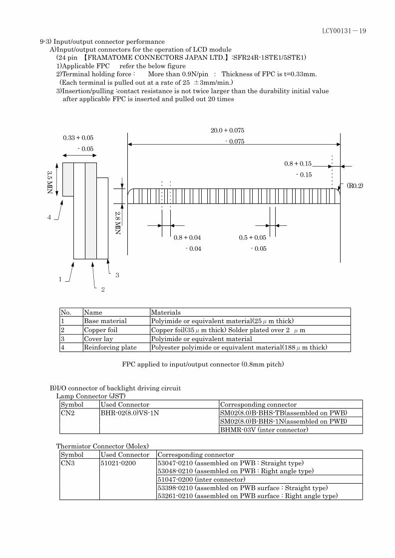
9-3) Input/output connector performance A)Input/output connectors for the operation of LCD module (24 pin 【FRAMATOME CONNECTORS JAPAN LTD.】:SFR24R-1STE1/5STE1) 1)Applicable FPC refer the below figure 2)Terminal holding force : More than 0.9N/pin : Thickness of FPC is t=0.33mm. (Each terminal is pulled out at a rate of 25 ±3mm/min.) 3)Insertion/pulling :contact resistance is not twice larger than the durability initial value after applicable FPC is inserted and pulled out 20 times
20.0 + 0.075 - 0.0750.33 + 0.05
- 0.05
2.8 MIN
3.5 MIN
4
1
2
3
0.5 + 0.05 - 0.05
0.8 + 0.15 - 0.15
0.8 + 0.04 - 0.04
(R0.2)
No. Name Materials 1 Base material Polyimide or equivalent material(25μm thick) 2 Copper foil Copper foil(35μm thick) Solder plated over 2 μm 3 Cover lay Polyimide or equivalent material 4 Reinforcing plate Polyester polyimide or equivalent material(188μm thick)
FPC applied to input/output connector (0.8mm pitch)
B)I/O connector of backlight driving circuit Lamp Connector (JST)
Symbol Used Connector Corresponding connector CN2 BHR-02(8.0)VS-1N SM02(8.0)B-BHS-TB(assembled on PWB)
SM02(8.0)B-BHS-1N(assembled on PWB) BHMR-03V (inter connector)
Thermistor Connector (Molex)
Symbol Used Connector Corresponding connector CN3 51021-0200 53047-0210 (assembled on PWB : Straight type)
53048-0210 (assembled on PWB : Right angle type) 51047-0200 (inter connector) 53398-0210 (assembled on PWB surface : Straight type) 53261-0210 (assembled on PWB surface : Right angle type)
LCY00131-20
(10) Display quality The display quality of the color TFT-LCD module shall be in compliance with the Delivery Inspection Standard.
(11) Handling instructions 11-1) Mounting of module The TFT-LCD module is designed to be mounted on equipment using the mounting tabs in the four corners of the module at the rear side. On mounting the module, as the M2.6 tapping screw fastening torque is 0.3 through
0. 5N・m(7mm length) is recommended, be sure to fix the module on the same plane, taking care not to wrap or twist the module. Don't reach the pressure of touch-switches of the set side to a module directly, because images may be disturbed. Please power off the module when you connect the input/output connector. Please connect the metallic shielding cases of the module and the ground pattern of the inverter circuit surely. If that connection is not perfect, there may be a possibility that the following problems happen. a). The noise from the backlight unit will increase. b). The output from inverter circuit will be unstable. Then, there may be a possibility that some problems happen. c). In some cases, a part of module will heat. 11-2) Precautions in mounting Polarizer which is made of soft material and susceptible to flaw must be handled carefully. Protective film (Laminator) is applied on the surface to protect it against scratches and dirts. It is recommended to peel off the laminator immediatery before the use, taking care of static electricity. Precautions in peeling off the laminator A) Working environment When the laminator is peeled off, static electricity may cause dust to stick to the polarizer surface. To avoid this, the following working environment is desirable. a) Floor:Conductive treatment of 1MΩ or more on the tile (conductive mat or conductive paint on the tile) b) Clean room free form dust and with an adhesive mat on the doorway c) Advisable humidity:50%~70% Advisable temperature:15℃~27℃ d) Workers shall wear conductive shoes, conductive work clothes, conductive gloves and an earth band. B) Working procedures a) Direct the wind of discharging blower somewhat downward to ensure that module is blown sufficiently. Keep the distance between module and discharging blower within 20 cm. b) Attach adhesive tape to the laminator part near discharging blower so as to protect polarizer against flaw. c) Peel off laminator, pulling adhesive tape slowly to your side taking 5 or more second. d) On peeling off the laminator, pass the module to the next work process to prevent the module to get dust.
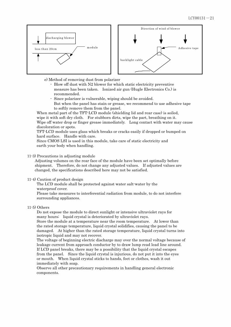
LCY00131-21
discharging blower
less than 20cm m odule
D irection of w ind of blow er
Adhesive tape
backlight cable
e) Method of removing dust from polarizer ・ Blow off dust with N2 blower for which static electricity preventive measure has been taken. Ionized air gun (Hugle Electronics Co.) is recommended. ・ Since polarizer is vulnerable, wiping should be avoided. But when the panel has stain or grease, we recommend to use adhesive tape to softly remove them from the panel. When metal part of the TFT-LCD module (shielding lid and rear case) is soiled, wipe it with soft dry cloth. For stubborn dirts, wipe the part, breathing on it. Wipe off water drop or finger grease immediately. Long contact with water may cause discoloration or spots. TFT-LCD module uses glass which breaks or cracks easily if dropped or bumped on hard surface. Handle with care. Since CMOS LSI is used in this module, take care of static electricity and earth your body when handling.
11-3) Precautions in adjusting module Adjusting volumes on the rear face of the module have been set optimally before shipment. Therefore, do not change any adjusted values. If adjusted values are changed, the specifications described here may not be satisfied. 11-4) Caution of product design The LCD module shall be protected against water salt-water by the waterproof cover. Please take measures to interferential radiation from module, to do not interfere surrounding appliances. 11-5) Others Do not expose the module to direct sunlight or intensive ultraviolet rays for many hours; liquid crystal is deteriorated by ultraviolet rays. Store the module at a temperature near the room temperature. At lower than the rated storage temperature, liquid crystal solidifies, causing the panel to be damaged. At higher than the rated storage temperature, liquid crystal turns into isotropic liquid and may not recover. The voltage of beginning electric discharge may over the normal voltage because of leakage current from approach conductor by to draw lump read lead line around. If LCD panel breaks, there may be a possibility that the liquid crystal escapes from the panel. Since the liquid crystal is injurious, do not put it into the eyes or mouth. When liquid crystal sticks to hands, feet or clothes, wash it out immediately with soap. Observe all other precautionary requirements in handling general electronic components.
LCY00131-22
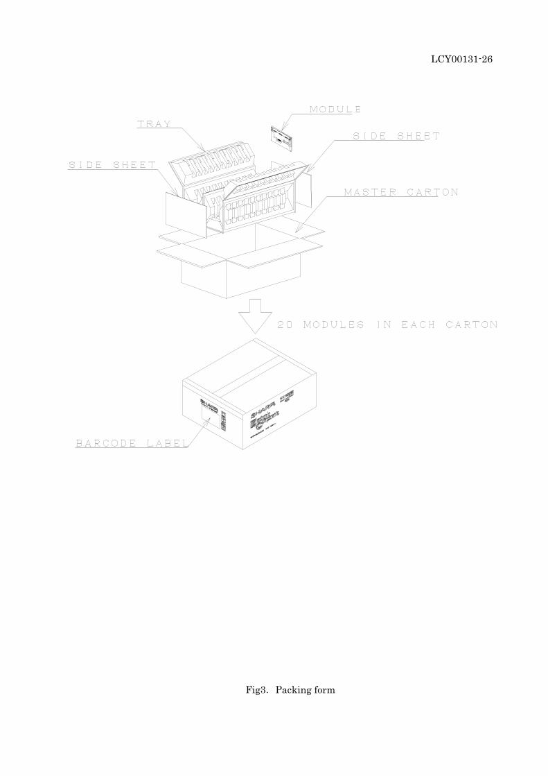
(12)Forwarding form 12-1)Fig.3 shows packing form. 12-2)Conditions for storage. ①Piling number of cartons : 10 ②Environment Temperature : 0~40℃ Humidity : 60%RH or less(at 40℃) No dew condensation at low temperature and high humidity. Atmosphere : Harmful gas, such as acid or alkali which bites electronic components and/or wires, must not be detected. Period :About 3 months Opening of the package : In order to prevent the LCD module from breakdown by electrostatic charges, please control the room humidity over 50%RH and open the package taking sufficient countermeasures against electrostatic charges, such as earth, etc. (13)Reliability test conditions Reliability test conditions for the TFT-LCD module are shown in Table 13. (14)Others 14-1)Indication of lot number The lot number is shown on a label. Attached location is shown in Fig.1(Outline Dimensions). Indicated contents of the label
LQ065T9BR51 ○○○○○○○○○ model No. lot No. Contents of lot No. the 1st figure ‥ production year (ex.2000 : 0) the 2nd figure ‥ production month 1,2,3,……,9,X,Y,Z the 3rd~7th figure ‥ serial No. 00001~ the 8th figure ‥ revision marks blank or A,B,C … the 9th figure ‥ production factory code blank or A,B,C …

LCY00131-23
Reliability test conditions for TFT-LCD module Table 13
Remark) Temperature condition is based on operating temperature conditions on (6)-Table 6.
No. Test items Test conditions 1
High temperature storage test
Ta=+85℃ 240H
2
Low temperature storage test
Ta=-30℃ 240H
3
High temperature And high humidity operating test
Tp=+50℃, 90~95%RH 240H
4
High temperature operating test
Tp=+85℃ 240H
5
Low temperature operating test
Tp=-30℃ 240H
6
Electro static discharge test
±200V, 200pF(0Ω) 1 times for each terminals
7
Shock test
980m/s2・6ms, ±X, ±Y, ±Z 3times for each direction (JIS C0041,A-7 condition C)
8
Vibration test
・Frequency range : 8~33.3Hz Stroke : 1.3mm
Sweep : 33.3Hz~400Hz ・Frequency range : 8~33.3Hz Acceleration : 28.4 m/s2 Cycle : 15 minutes X,Z 2 hours for each directions, 4 hours for Y direction (total 8 hours) 【caution】 (JIS D1601)
9
Heat shock test
Tp=-30~+85℃ / 200cycles (0.5H) (0.5H)
【Note】Ta=Ambient temperature, Tp=Panel temperature 【Check items】In the standard condition, there shall be no practical problems that may affect the display function. 【Caution】X,Y,Z directions are shown as follows
X Y
Z
LCY000131-24
Fig1.Outline dimension of TFT-LCD module
LCY00131-25
Fig2.Construction of TFT-LCD module
LCY00131-26
Fig3.Packing form

VRVRVRVR VGVGVGVG VBVBVBVB
FRPVFRPVFRPVFRPV
H S YH S YH S YH S Y
SYNSYNSYNSYN
VIDC
(VSM)
τrHI1 τfHI1
τD
PAL; 1H=64.0μs (typ.) NTSC;1H=63.5μs (typ.)
τfHO τrHO τHO
τpd1 τHI
τpd2
Black
White
White
Black
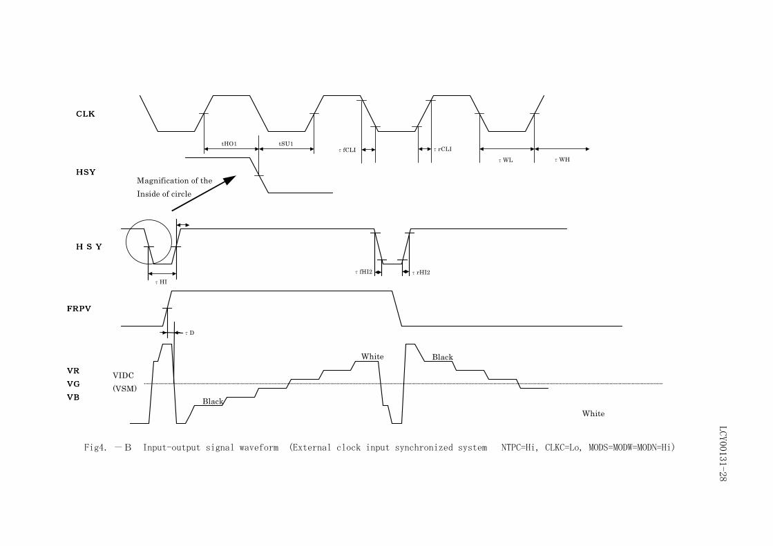
Fig.4-A Input-output siganl waveform (NTSC,PAL system CLKC=Hi)
LCY00131-27
VRVRVRVR VGVGVGVG VBVBVBVB
FRPVFRPVFRPVFRPV
H S YH S YH S YH S Y
CLKCLKCLKCLK
HSYHSYHSYHSY
VIDC (VSM)
τD
tSU1 tHO1
τfHI2 τrHI2
τWH τWL τrCLI τfCLI
τHI
Black
White
White
Black
Magnification of the Inside of circle
Fig4.-B Input-output signal waveform (External clock input synchronized system NTPC=Hi, CLKC=Lo, MODS=MODW=MODN=Hi)
LCY00131-28
COMCOMCOMCOM
FRPTFRPTFRPTFRPT
VCDC
τDC
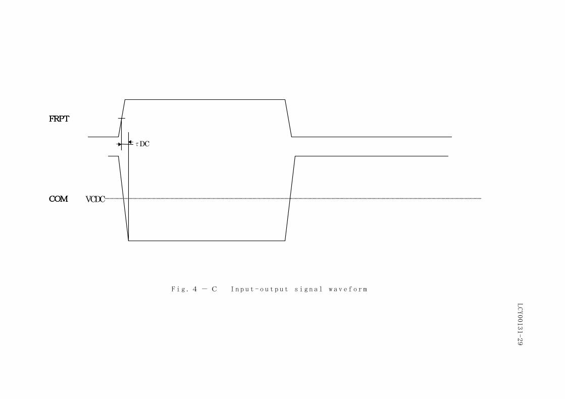
F i g .4 - C I n p u t - o u t p u t s i g n a l w a v e f o r m
LCY00131-29
VCSVCSVCSVCS
HSYHSYHSYHSY
50.1μs 13.1μs
Masking period Masking period Period of showing image
Fig.4-G Input-output signal waveform (Normal mode、NTSC,PAL system CLKC=Hi, MODS=Hi, MODW=Lo, MODN=Hi)
LCY00131-33
VCSVCSVCSVCS
VSYVSYVSYVSY NTSC:Full・wide・normal 20~253H
Cinema 49~224H
Wide2 42~228H
PAL :Full・wide・normal 26~298H
Cinema 49~282H
Wide2 35~291H
Masking period Masking period Period of showing image
Fig4.-H Input-output signal waveform (Vertical mask mode、NTSC,PAL system VMSW=Lo)
LCY00131-34
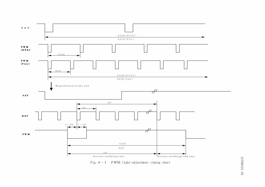
P W MP W MP W MP W M ( N T S C( N T S C( N T S C( N T S C
P W MP W MP W MP W M ( P A L )( P A L )( P A L )( P A L )
P W MP W MP W MP W M
V S YV S YV S YV S Y
H S YH S YH S YH S Y
V S YV S YV S YV S Y
6 2 5 H ( P A L )
5 2 5 H ( N T S C )
8 9 H
1 0 5 H
6 2 5 H ( P A L )
5 2 5 H ( N T S C )
n H
n H
1 H
1 / 2 H 1 / 2 H
8 9 H
1 0 5 H
I n v e r t e r o s c i l l a t i n g t i m e I n v e r t e r o s c i l l a t i n g - s t o p t i m e
M a g n i f i c a t i o n o f t i m e a x i s
Fig.4-I PWM light-adjustment timing chart
LCY00131-35
LCY00131-36
Photodetector
(including luminosity factor)
Center
TFT-LCD module LCD panel
DC/AC inverter driving frequency:(49kHz)
Fig.5.Measurement method of optical characteristics(Transmissive mode)
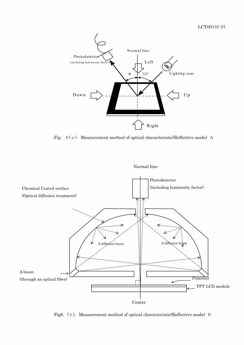
LCY00131-37 Fig.6(a).Measurement method of optical characteristic(Reflective mode) A Fig6.(b).Measurement method of optical characteristic(Reflective mode) B
TFT-LCD module
Polarizer
Photodetector (including luminosity factor) Chemical Coated surface
(Optical diffusion treatment)
A diffusion beam A diffusion beam
A beam (through an optical fiber)
Normal line
Center
Lighting sour
Photodetector
30°θ
U pD ow n
R ight
Left
N orm al line
(inc lud ing lum ino sity facto r)
LCY00131- 38
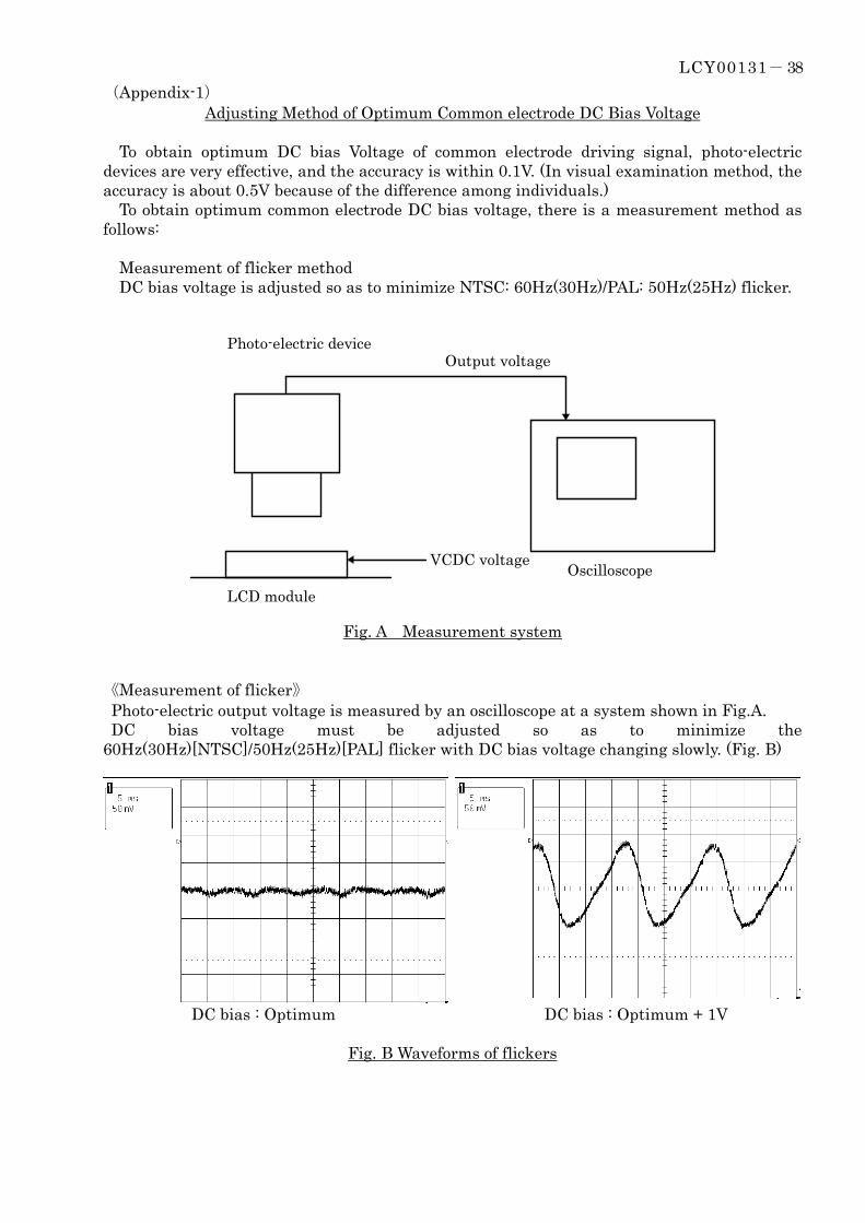
(Appendix-1) Adjusting Method of Optimum Common electrode DC Bias Voltage
To obtain optimum DC bias Voltage of common electrode driving signal, photo-electric devices are very effective, and the accuracy is within 0.1V. (In visual examination method, the accuracy is about 0.5V because of the difference among individuals.) To obtain optimum common electrode DC bias voltage, there is a measurement method as follows: Measurement of flicker method DC bias voltage is adjusted so as to minimize NTSC: 60Hz(30Hz)/PAL: 50Hz(25Hz) flicker.
Output voltagePhoto-electric device
LCD module
VCDC voltage Oscilloscope
Fig. A Measurement system
《Measurement of flicker》 Photo-electric output voltage is measured by an oscilloscope at a system shown in Fig.A. DC bias voltage must be adjusted so as to minimize the 60Hz(30Hz)[NTSC]/50Hz(25Hz)[PAL] flicker with DC bias voltage changing slowly. (Fig. B)
DC bias : Optimum DC bias : Optimum + 1V
Fig. B Waveforms of flickers
SPECIFICATIONS ARE SUBJECT TO CHANGE WITHOUT NOTICE.Suggested applications (if any) are for standard use; See Important Restrictions for limitations on special applications. See Limited �Warranty for SHARP’s product warranty. The Limited Warranty is in lieu, and exclusive of, all other warranties, express or implied. �ALL EXPRESS AND IMPLIED WARRANTIES, INCLUDING THE WARRANTIES OF MERCHANTABILITY, FITNESS FOR USE AND �FITNESS FOR A PARTICULAR PURPOSE, ARE SPECIFICALLY EXCLUDED. In no event will SHARP be liable, or in any way responsible,�for any incidental or consequential economic or property damage.
NORTH AMERICA EUROPE JAPAN
SHARP Microelectronics of the Americas5700 NW Pacific Rim Blvd.Camas, WA 98607, U.S.A.Phone: (1) 360-834-2500Fax: (1) 360-834-8903Fast Info: (1) 800-833-9437www.sharpsma.com
SHARP Microelectronics EuropeDivision of Sharp Electronics (Europe) GmbHSonninstrasse 320097 Hamburg, GermanyPhone: (49) 40-2376-2286Fax: (49) 40-2376-2232www.sharpsme.com
SHARP CorporationElectronic Components & Devices22-22 Nagaike-cho, Abeno-KuOsaka 545-8522, JapanPhone: (81) 6-6621-1221Fax: (81) 6117-725300/6117-725301www.sharp-world.com
TAIWAN SINGAPORE KOREA
SHARP Electronic Components(Taiwan) Corporation8F-A, No. 16, Sec. 4, Nanking E. Rd.Taipei, Taiwan, Republic of ChinaPhone: (886) 2-2577-7341Fax: (886) 2-2577-7326/2-2577-7328
SHARP Electronics (Singapore) PTE., Ltd.438A, Alexandra Road, #05-01/02Alexandra Technopark, Singapore 119967Phone: (65) 271-3566Fax: (65) 271-3855
SHARP Electronic Components(Korea) CorporationRM 501 Geosung B/D, 541Dohwa-dong, Mapo-kuSeoul 121-701, KoreaPhone: (82) 2-711-5813 ~ 8Fax: (82) 2-711-5819
CHINA HONG KONG
SHARP Microelectronics of China(Shanghai) Co., Ltd.28 Xin Jin Qiao Road King Tower 16FPudong Shanghai, 201206 P.R. ChinaPhone: (86) 21-5854-7710/21-5834-6056Fax: (86) 21-5854-4340/21-5834-6057Head Office:No. 360, Bashen Road, Xin Development Bldg. 22Waigaoqiao Free Trade Zone Shanghai200131 P.R. ChinaEmail: [email protected]
SHARP-ROXY (Hong Kong) Ltd.3rd Business Division,17/F, Admiralty Centre, Tower 118 Harcourt Road, Hong KongPhone: (852) 28229311Fax: (852) 28660779www.sharp.com.hkShenzhen Representative Office:Room 13B1, Tower C,Electronics Science & Technology BuildingShen Nan Zhong RoadShenzhen, P.R. ChinaPhone: (86) 755-3273731Fax: (86) 755-3273735