Embed Size (px)
Citation preview
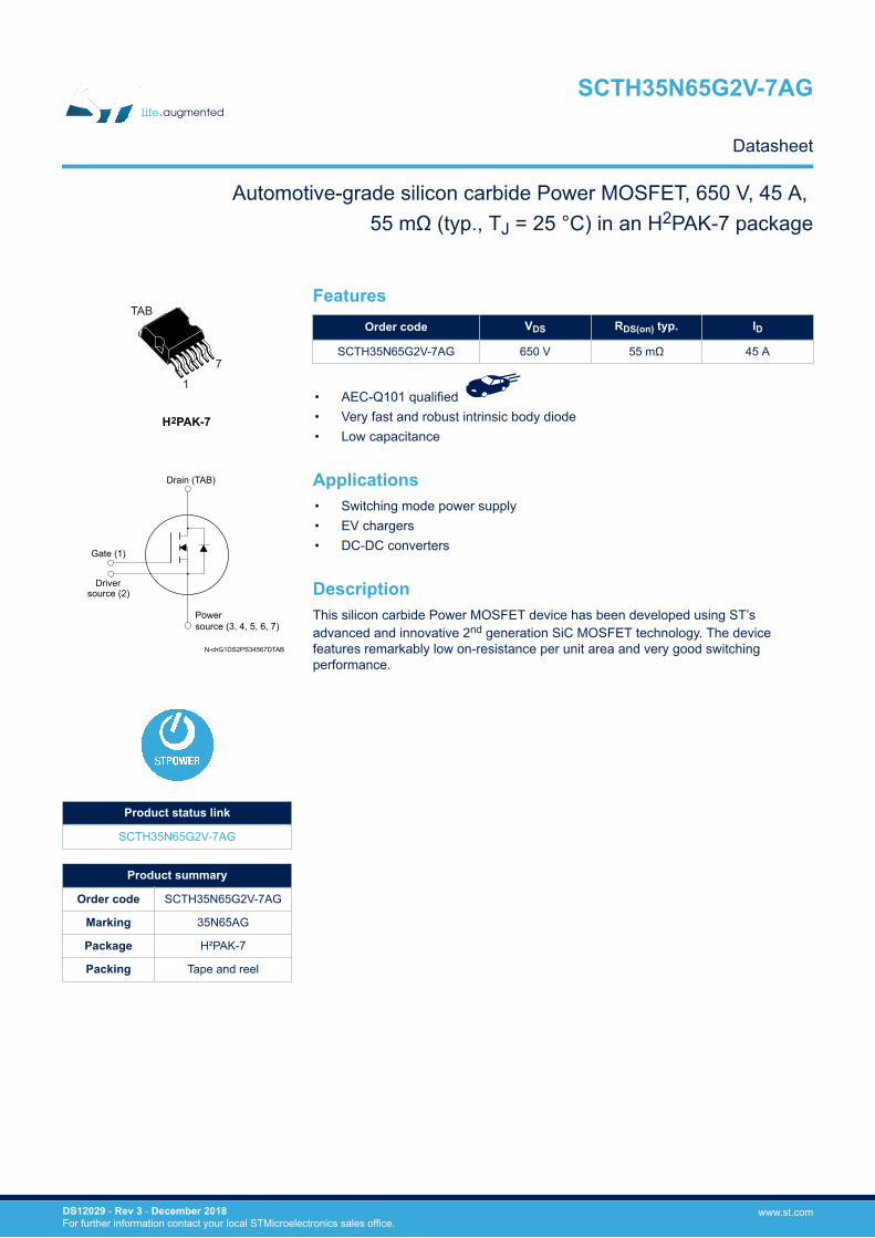
TAB
7
1
H2PAK-7
Drain (TAB)
Gate (1)
Driversource (2)
Powersource (3, 4, 5, 6, 7)
N-chG1DS2PS34567DTAB
FeaturesOrder code VDS RDS(on) typ. ID
SCTH35N65G2V-7AG 650 V 55 mΩ 45 A
• AEC-Q101 qualified • Very fast and robust intrinsic body diode• Low capacitance
Applications• Switching mode power supply• EV chargers• DC-DC converters
DescriptionThis silicon carbide Power MOSFET device has been developed using ST’sadvanced and innovative 2nd generation SiC MOSFET technology. The devicefeatures remarkably low on-resistance per unit area and very good switchingperformance.
Product status link
SCTH35N65G2V-7AG
Product summary
Order code SCTH35N65G2V-7AG
Marking 35N65AG
Package H²PAK-7
Packing Tape and reel
Automotive-grade silicon carbide Power MOSFET, 650 V, 45 A, 55 mΩ (typ., TJ = 25 °C) in an H2PAK-7 package
SCTH35N65G2V-7AG
Datasheet
DS12029 - Rev 3 - December 2018For further information contact your local STMicroelectronics sales office.
www.st.com

1 Electrical ratings
Table 1. Absolute maximum ratings
Symbol Parameter Value Unit
VGSGate-source voltage -10 to 22
VGate-source voltage (recommended operational values) -5 to 20
VDS Drain-source voltage 650 V
IDDrain current (continuous) at TC = 25 °C 45
ADrain current (continuous) at TC = 100 °C 35
IDM(1) Drain current (pulsed) 90 A
PTOT Total power dissipation at TC = 25 °C 208 W
Tstg Storage temperature range-55 to 175
°C
TJ Operating junction temperature range °C
1. Pulse width is limited by safe operating area.
Table 2. Thermal data
Symbol Parameter Value Unit
Rthj-case Thermal resistance junction-case 0.72 °C/W
Rthj-amb Thermal resistance junction-ambient 62.5 °C/W
SCTH35N65G2V-7AGElectrical ratings
DS12029 - Rev 3 page 2/15
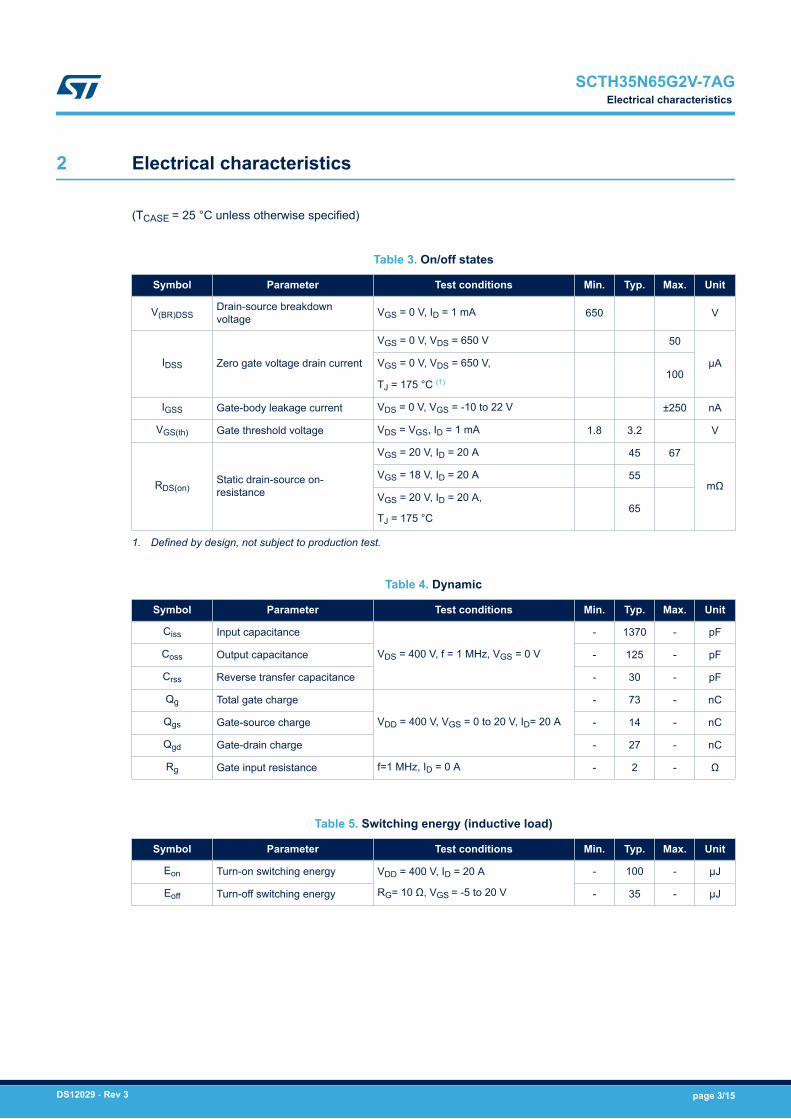
2 Electrical characteristics
(TCASE = 25 °C unless otherwise specified)
Table 3. On/off states
Symbol Parameter Test conditions Min. Typ. Max. Unit
V(BR)DSSDrain-source breakdownvoltage VGS = 0 V, ID = 1 mA 650 V
IDSS Zero gate voltage drain current
VGS = 0 V, VDS = 650 V 50
µAVGS = 0 V, VDS = 650 V,
TJ = 175 °C (1)100
IGSS Gate-body leakage current VDS = 0 V, VGS = -10 to 22 V ±250 nA
VGS(th) Gate threshold voltage VDS = VGS, ID = 1 mA 1.8 3.2 V
RDS(on)Static drain-source on-resistance
VGS = 20 V, ID = 20 A 45 67
mΩVGS = 18 V, ID = 20 A 55
VGS = 20 V, ID = 20 A,
TJ = 175 °C65
1. Defined by design, not subject to production test.
Table 4. Dynamic
Symbol Parameter Test conditions Min. Typ. Max. Unit
Ciss Input capacitance
VDS = 400 V, f = 1 MHz, VGS = 0 V
- 1370 - pF
Coss Output capacitance - 125 - pF
Crss Reverse transfer capacitance - 30 - pF
Qg Total gate charge
VDD = 400 V, VGS = 0 to 20 V, ID= 20 A
- 73 - nC
Qgs Gate-source charge - 14 - nC
Qgd Gate-drain charge - 27 - nC
Rg Gate input resistance f=1 MHz, ID = 0 A - 2 - Ω
Table 5. Switching energy (inductive load)
Symbol Parameter Test conditions Min. Typ. Max. Unit
Eon Turn-on switching energy VDD = 400 V, ID = 20 A
RG= 10 Ω, VGS = -5 to 20 V
- 100 - µJ
Eoff Turn-off switching energy - 35 - µJ
SCTH35N65G2V-7AGElectrical characteristics
DS12029 - Rev 3 page 3/15
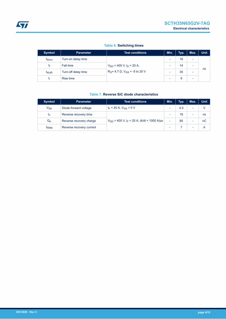
Table 6. Switching times
Symbol Parameter Test conditions Min. Typ. Max. Unit
td(on) Turn-on delay time
VDD = 400 V, ID = 20 A,
RG= 4.7 Ω, VGS = -5 to 20 V
- 16 -
nstf Fall time - 14 -
td(off) Turn-off delay time - 35 -
tr Rise time - 9 -
Table 7. Reverse SiC diode characteristics
Symbol Parameter Test conditions Min. Typ. Max. Unit
VSD Diode forward voltage IF = 20 A, VGS = 0 V - 4.5 - V
trr Reverse recovery time
VDD = 400 V, IF = 20 A, di/dt = 1000 A/μs
- 18 - ns
Qrr Reverse recovery charge - 85 - nC
IRRM Reverse recovery current - 7 - A
SCTH35N65G2V-7AGElectrical characteristics
DS12029 - Rev 3 page 4/15

2.1 Electrical characteristics (curves)
Figure 1. Safe operating area
GADG140220171448SOA
10 1
10 0
10 -1
10 -1 10 0 10 1 10 2
ID (A)
VDS (V)
Operation in this areais limited by RDS(on)
tp =100 µs
tp =1 ms
tp =10 ms
TC = 25 °C,TJ ≤ 175 °C,single pulse
Figure 2. Thermal impedance
GADG140220171449ZTH
10 -1
10 -2
10 -5 10 -4 10 -3 10 -2 10 -1
K
tp (s)
single pulse
Figure 3. Output characteristics (TJ= 25 °C)
SIC140220171450OC25
80
60
40
20
00 2 4 6 8 10 12
ID (A)
VDS (V)
VGS = 20 V
VGS = 16 V
VGS = 6 VVGS = 8 V
VGS = 10 V
VGS = 12 V
VGS = 14 V
Figure 4. Output characteristics (TJ= 175 °C)
SIC140220171450OC175
80
60
40
20
00 2 4 6 8 10 12
ID (A)
VDS (V)
VGS = 6 V
VGS = 8 V
VGS = 10 V
VGS = 12 V
VGS = 14 VVGS = 16 VVGS = 20 V
Figure 5. Transfer characteristics
GADG140220171450TCH
80
60
40
20
00 4 8 12 16
ID (A)
VGS (V)
VDS = 10 V
TJ = 175 °C
TJ = 25 °C
Figure 6. Power total dissipation
SIC140220171451PDT
200
160
120
80
40
00 50 100 150
PTOT (W)
TC (°C)
TJ ≤ 175 °C
SCTH35N65G2V-7AGElectrical characteristics (curves)
DS12029 - Rev 3 page 5/15

Figure 7. Gate charge vs gate-source voltage
GADG140220171452QVG
20
16
12
8
4
00 10 20 30 40 50 60 70
VGS (V)
Qg (nC)
VDD = 400 VID = 20 A
Figure 8. Capacitance variations
GADG140220171452CVR
10 3
10 2
10 1
10 -1 10 0 10 1 10 2
C (pF)
VDS (V)
CISS
COSS
CRSS
f = 1 MHz
Figure 9. Switching energy vs. drain current
SIC140220171454SLC
1000
800
600
400
200
00 20 40 60
E (μJ)
ID (A)
Etot
Eon
Eoff
VDD = 400 V, RG = 4.7 Ω,
VGS = -5 to 20 V
Figure 10. Switching energy vs. junction temperature
SIC140220171455SLT
140
120
100
80
60
40
20
00 50 100 150
E (μJ)
TJ (°C)
Etot
Eon
Eoff
VDD = 400 V, RG = 4.7 Ω,ID = 20 A, VGS = -5 to 20 V
Figure 11. Normalized V(BR)DSS vs. temperature
GADG140220171455BDV
1.06
1.04
1.02
1
0.98
0.96
0.94-75 -25 25 75 125 175
V(BR)DSS (norm.)
TJ (°C)
ID = 1 mA
Figure 12. Normalized gate threshold voltage vs.temperature
GADG140220171458VTH
1.4
1.2
1
0.8
0.6
0.4-75 -25 25 75 125 175
VGS(th) (norm.)
TJ (°C)
ID = 1 mA
SCTH35N65G2V-7AGElectrical characteristics (curves)
DS12029 - Rev 3 page 6/15

Figure 13. Normalized on-resistance vs. temperature
GADG140220171458RON
2
1.5
1
0.5
0-75 -25 25 75 125 175
RDS(on) (norm.)
TJ (°C)
VGS = 20 V
Figure 14. Reverse conduction characteristics (TJ= 25 °C)
SIC140220171501RRT25
-20
-40
-60
-80
-100-7 -6 -5 -4 -3 -2 -1
ID (A)
VDS (V)
VGS = 10 V
VGS = 5 V
VGS = -5 V
VGS = -2 V
VGS = 0 V
Figure 15. Reverse conduction characteristics (TJ= 175 °C)
SIC140220171502RRT175
-20
-40
-60
-80
-100-7 -6 -5 -4 -3 -2 -1
ID (A)
VDS (V)
VGS = 10 V
VGS = 5 V
VGS = -5 V
VGS = -2 V
VGS = 0 V
SCTH35N65G2V-7AGElectrical characteristics (curves)
DS12029 - Rev 3 page 7/15

3 Test circuits
Figure 16. Test circuit for resistive load switching times
AM01468v1
VD
RG
RL
D.U.T.
2200μF VDD
3.3μF+
pulse width
VGS
Figure 17. Test circuit for gate charge behavior
AM01469v1
47 kΩ1 kΩ
47 kΩ
2.7 kΩ
1 kΩ
12 V
IG= CONST100 Ω
100 nF
D.U.T.
+pulse width
VGS
2200μF
VG
VDD
Figure 18. Test circuit for inductive load switching anddiode recovery times
AM01470v1
AD
D.U.T.S
B
G
25 Ω
A A
B B
RG
GD
S
100 µH
µF3.3 1000
µF VDD
D.U.T.
+
_
+
fastdiode
Figure 19. Unclamped inductive load test circuit
AM01471v1
VD
ID
D.U.T.
L
VDD+
pulse width
Vi
3.3µF
2200µF
Figure 20. Unclamped inductive waveform
AM01472v1
V(BR)DSS
VDDVDD
VD
IDM
ID
Figure 21. Switching time waveform
AM01473v1
0
VGS 90%
VDS
90%
10%
90%
10%
10%
ton
td(on) tr
0
toff
td(off) tf
SCTH35N65G2V-7AGTest circuits
DS12029 - Rev 3 page 8/15

4 Package information
In order to meet environmental requirements, ST offers these devices in different grades of ECOPACK®
packages, depending on their level of environmental compliance. ECOPACK® specifications, grade definitionsand product status are available at: www.st.com. ECOPACK® is an ST trademark.
4.1 H²PAK-7 package information
Figure 22. H²PAK-7 package outline
DM00249216_4
SCTH35N65G2V-7AGPackage information
DS12029 - Rev 3 page 9/15
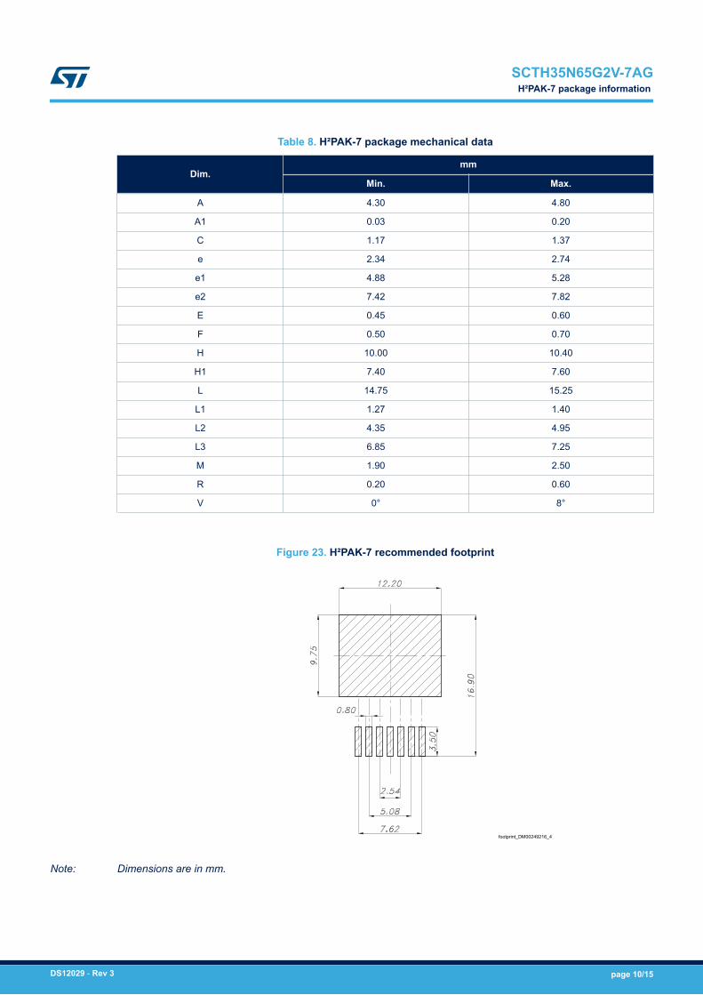
Table 8. H²PAK-7 package mechanical data
Dim.mm
Min. Max.
A 4.30 4.80
A1 0.03 0.20
C 1.17 1.37
e 2.34 2.74
e1 4.88 5.28
e2 7.42 7.82
E 0.45 0.60
F 0.50 0.70
H 10.00 10.40
H1 7.40 7.60
L 14.75 15.25
L1 1.27 1.40
L2 4.35 4.95
L3 6.85 7.25
M 1.90 2.50
R 0.20 0.60
V 0° 8°
Figure 23. H²PAK-7 recommended footprint
footprint_DM00249216_4
Note: Dimensions are in mm.
SCTH35N65G2V-7AGH²PAK-7 package information
DS12029 - Rev 3 page 10/15

4.2 Packing information
Figure 24. Tape outline
P1A0 D1
P0
FW
E
D
B0K0
T
User direction of feed
P2
10 pitches cumulativetolerance on tape +/- 0.2 mm
User direction of feed
R
Bending radius
Top covertape
AM08852v2
SCTH35N65G2V-7AGPacking information
DS12029 - Rev 3 page 11/15

Figure 25. Reel outline
A
D
B
Full radius
Tape slotIn core for
Tape start
G measured
At hub
C
N
REEL DIMENSIONS
40 mm min.
Access hole
At slot location
T
Table 9. Tape and reel mechanical data
Tape Reel
Dim.mm
Dim.mm
Min. Max. Min. Max.
A0 10.5 10.7 A 330
B0 15.7 15.9 B 1.5
D 1.5 1.6 C 12.8 13.2
D1 1.59 1.61 D 20.2
E 1.65 1.85 G 24.4 26.4
F 11.4 11.6 N 100
K0 4.8 5.0 T 30.4
P0 3.9 4.1
P1 11.9 12.1 Base quantity 1000
P2 1.9 2.1 Bulk quantity 1000
R 50
T 0.25 0.35
W 23.7 24.3
SCTH35N65G2V-7AGPacking information
DS12029 - Rev 3 page 12/15
Revision history
Table 10. Document revision history
Date Version Changes
17-Feb-2017 1 First release.
13-Dec-2017 2
Updated document title.
Updated Table 4: "On/off states".
Minor text changes.
13-Dec-2018 3
Datasheet promoted from preliminary data to production data.
Modified title and features on cover page.
Minor text changes.
SCTH35N65G2V-7AG
DS12029 - Rev 3 page 13/15
Contents
1 Electrical ratings . . . . . . . . . . . . . . . . . . . . . . . . . . . . . . . . . . . . . . . . . . . . . . . . . . . . . . . . . . . . . . . . . .2
2 Electrical characteristics. . . . . . . . . . . . . . . . . . . . . . . . . . . . . . . . . . . . . . . . . . . . . . . . . . . . . . . . . . .3
2.1 Electrical characteristics (curves) . . . . . . . . . . . . . . . . . . . . . . . . . . . . . . . . . . . . . . . . . . . . . . . . . 5
3 Test circuits . . . . . . . . . . . . . . . . . . . . . . . . . . . . . . . . . . . . . . . . . . . . . . . . . . . . . . . . . . . . . . . . . . . . . . .8
4 Package information. . . . . . . . . . . . . . . . . . . . . . . . . . . . . . . . . . . . . . . . . . . . . . . . . . . . . . . . . . . . . . .9
4.1 H²PAK-7 package information . . . . . . . . . . . . . . . . . . . . . . . . . . . . . . . . . . . . . . . . . . . . . . . . . . . . 9
4.2 Packing information . . . . . . . . . . . . . . . . . . . . . . . . . . . . . . . . . . . . . . . . . . . . . . . . . . . . . . . . . . . 10
Revision history . . . . . . . . . . . . . . . . . . . . . . . . . . . . . . . . . . . . . . . . . . . . . . . . . . . . . . . . . . . . . . . . . . . . . . .13
SCTH35N65G2V-7AGContents
DS12029 - Rev 3 page 14/15
IMPORTANT NOTICE – PLEASE READ CAREFULLY
STMicroelectronics NV and its subsidiaries (“ST”) reserve the right to make changes, corrections, enhancements, modifications, and improvements to STproducts and/or to this document at any time without notice. Purchasers should obtain the latest relevant information on ST products before placing orders. STproducts are sold pursuant to ST’s terms and conditions of sale in place at the time of order acknowledgement.
Purchasers are solely responsible for the choice, selection, and use of ST products and ST assumes no liability for application assistance or the design ofPurchasers’ products.
No license, express or implied, to any intellectual property right is granted by ST herein.
Resale of ST products with provisions different from the information set forth herein shall void any warranty granted by ST for such product.
ST and the ST logo are trademarks of ST. All other product or service names are the property of their respective owners.
Information in this document supersedes and replaces information previously supplied in any prior versions of this document.
© 2018 STMicroelectronics – All rights reserved
SCTH35N65G2V-7AG
DS12029 - Rev 3 page 15/15