Embed Size (px)
Citation preview
Datasheet
RL78/L12
RENESAS MCU
Integrated LCD controller/driver, True Low Power Platform (as low as 62.5 µA/MHz, and 0.64 µA for RTC + LVD), 1.6 V to 5.5 V operation, 8 to 32 Kbyte Flash, 31 DMIPS at 24 MHz, for All LCD Based Applications
R01DS0157EJ0210 Rev.2.10 Sep 30, 2016
Page 1 of 131
R01DS0157EJ0210Rev.2.10
Sep 30, 2016
1. OUTLINE
1.1 Features
Ultra-Low Power Technology • 1.6 V to 5.5 V operation from a single supply • Stop (RAM retained): 0.23 µA, (LVD enabled): 0.31 µA • Halt (RTC + LVD): 0.64 µA • Supports snooze • Operating: 62.5 µA/MHz • LCD operating current (Capacitor split method): 0.12 µA • LCD operating current (Internal voltage boost method):
0.63 µA (VDD = 3.0 V)
16-bit RL78 CPU Core • Delivers 31 DMIPS at maximum operating frequency of
24 MHz • Instruction Execution: 86% of instructions can be
executed in 1 to 2 clock cycles • CISC Architecture (Harvard) with 3-stage pipeline • Multiply Signed & Unsigned: 16 x 16 to 32-bit result in 1
clock cycle • MAC: 16 x 16 to 32-bit result in 2 clock cycles • 16-bit barrel shifter for shift & rotate in 1 clock cycle • 1-wire on-chip debug function
Code Flash Memory • Density: 8 KB to 32 KB • Block size: 1 KB • On-chip single voltage flash memory with protection
from block erase/writing • Self-programming with flash shield window function
Data Flash Memory • Data flash with background operation • Data flash size: 2 KB size • Erase cycles: 1 Million (typ.) • Erase/programming voltage: 1.8 V to 5.5 V
RAM • 1 KB and 1.5 KB size options • Supports operands or instructions • Back-up retention in all modes
High-speed On-chip Oscillator • 24 MHz with +/− 1% accuracy over voltage (1.8 V to 5.5
V) and temperature (−20°C to 85°C) • Pre-configured settings: 24 MHz, 16 MHz, 12 MHz, 8
MHz, 6 MHz, 4 MHz, 3 MHz, 2 MHz & 1 MHz
Reset and Supply Management • Power-on reset (POR) monitor/generator • Low voltage detection (LVD) with 14 setting options
(Interrupt and/or reset function)
LCD Controller/Driver • Up to 35 seg x 8 com or 39 seg x 4 com • Supports capacitor split method, internal voltage boost
method and resistance division method • Supports waveform types A and B • Supports LCD contrast adjustment (16 steps) • Supports LCD blinking
Direct Memory Access (DMA) Controller • Up to 2 fully programmable channels • Transfer unit: 8- or 16-bit
Multiple Communication Interfaces • Up to 1 × I2C multi-master • Up to 2 × CSI/SPI (7-, 8-bit) • Up to 1 × UART (7-, 8-, 9-bit) • Up to 1 × LIN
Extended-Function Timers • Multi-function 16-bit timers: Up to 8 channels • Real-time clock (RTC): 1 channel (full calendar and
alarm function with watch correction function) • Interval Timer: 12-bit, 1 channel • 15 kHz watchdog timer: 1 channel (window function)
Rich Analog • ADC: Up to 10 channels, 10-bit resolution, 2.1 µs
conversion time • Supports 1.6 V • Internal reference voltage (1.45 V) • On-chip temperature sensor
Safety Features (IEC or UL 60730 compliance) • Flash memory CRC calculation • RAM parity error check • RAM write protection • SFR write protection • Illegal memory access detection • Clock frequency detection • ADC self-test
General Purpose I/O • 5V tolerant, high-current (up to 20 mA per pin) • Open-Drain, Internal Pull-up support
Operating Ambient Temperature • TA: −40 °C to +85 °C (A: Consumer applications) • TA: −40 °C to +105 °C (G: Industrial applications)
Package Type and Pin Count From 7mm x 7mm to 12mm x 12mm QFP: 32, 44, 48, 52, 64
RL78/L12 1. OUTLINE
R01DS0157EJ0210 Rev.2.10 Sep 30, 2016
Page 2 of 131
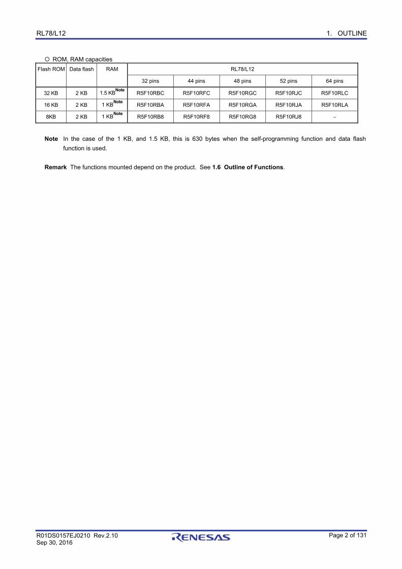
ROM, RAM capacities
Flash ROM Data flash RAM RL78/L12
32 pins 44 pins 48 pins 52 pins 64 pins
32 KB 2 KB 1.5 KBNote
R5F10RBC R5F10RFC R5F10RGC R5F10RJC R5F10RLC
16 KB 2 KB 1 KBNote
R5F10RBA R5F10RFA R5F10RGA R5F10RJA R5F10RLA
8KB 2 KB 1 KBNote
R5F10RB8 R5F10RF8 R5F10RG8 R5F10RJ8 −
Note In the case of the 1 KB, and 1.5 KB, this is 630 bytes when the self-programming function and data flash
function is used.
Remark The functions mounted depend on the product. See 1.6 Outline of Functions.
RL78/L12 1. OUTLINE
R01DS0157EJ0210 Rev.2.10 Sep 30, 2016
Page 3 of 131
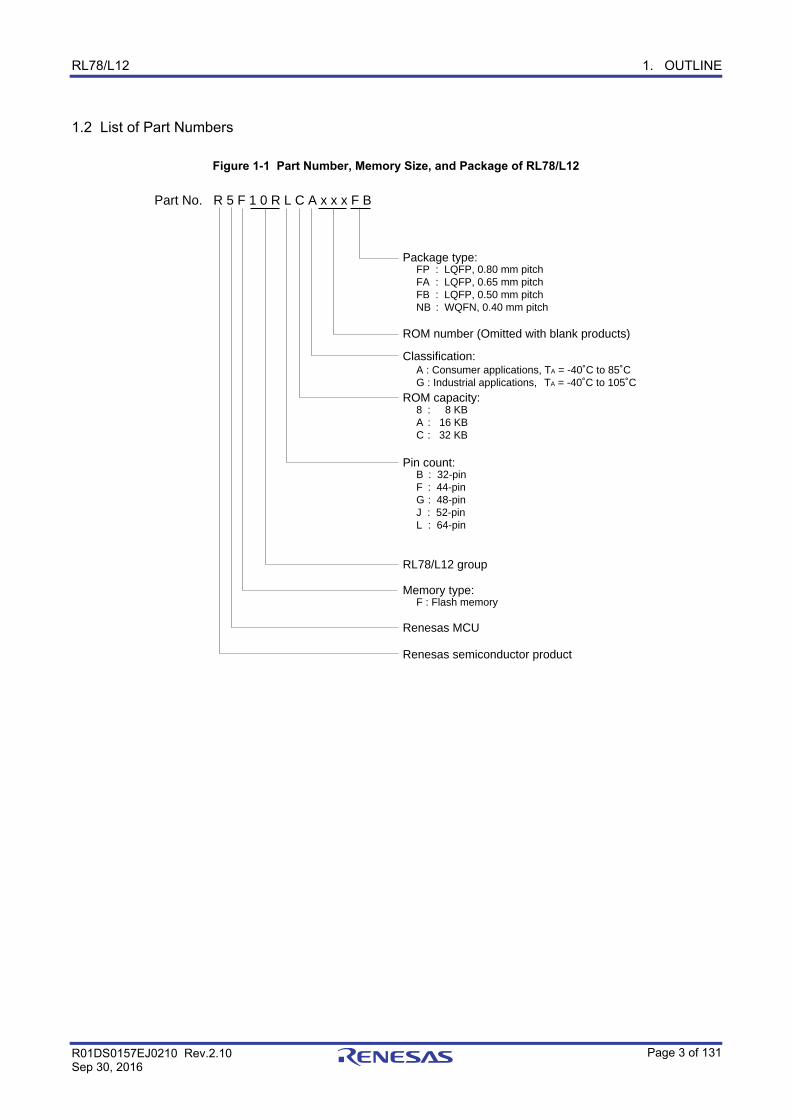
1.2 List of Part Numbers
Figure 1-1 Part Number, Memory Size, and Package of RL78/L12
Part No. R 5 F 1 0 R L C A x x x F B
Package type:
ROM number (Omitted with blank products)
ROM capacity:
RL78/L12 group
Renesas MCU
Renesas semiconductor product
FP : LQFP, 0.80 mm pitchFA : LQFP, 0.65 mm pitchFB : LQFP, 0.50 mm pitchNB : WQFN, 0.40 mm pitch
8 : 8 KBA : 16 KBC : 32 KB
Pin count:B : 32-pinF : 44-pinG : 48-pinJ : 52-pinL : 64-pin
Classification:A : Consumer applications, TA = -40˚C to 85˚CG : Industrial applications, TA = -40˚C to 105˚C
Memory type:F : Flash memory
RL78/L12 1. OUTLINE
R01DS0157EJ0210 Rev.2.10 Sep 30, 2016
Page 4 of 131
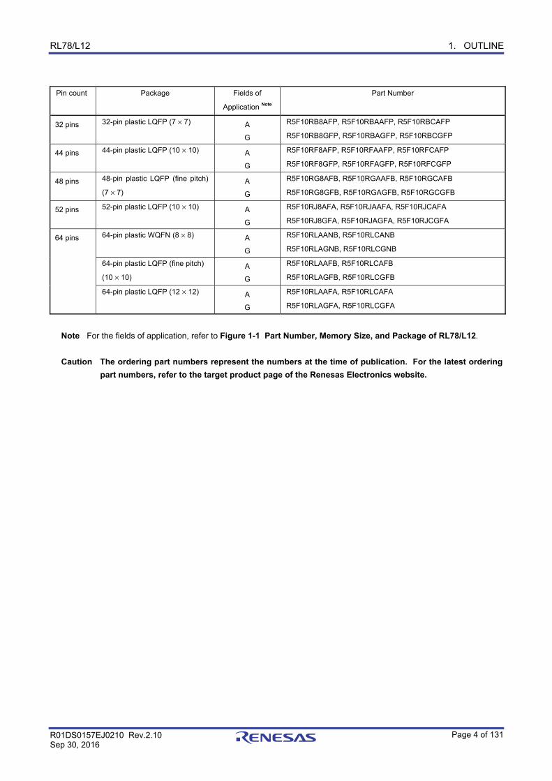
Pin count Package Fields of
Application Note
Part Number
32 pins 32-pin plastic LQFP (7 × 7) A
G
R5F10RB8AFP, R5F10RBAAFP, R5F10RBCAFP
R5F10RB8GFP, R5F10RBAGFP, R5F10RBCGFP
44 pins 44-pin plastic LQFP (10 × 10) A
G
R5F10RF8AFP, R5F10RFAAFP, R5F10RFCAFP
R5F10RF8GFP, R5F10RFAGFP, R5F10RFCGFP
48 pins 48-pin plastic LQFP (fine pitch)
(7 × 7)
A
G
R5F10RG8AFB, R5F10RGAAFB, R5F10RGCAFB
R5F10RG8GFB, R5F10RGAGFB, R5F10RGCGFB
52 pins 52-pin plastic LQFP (10 × 10) A
G
R5F10RJ8AFA, R5F10RJAAFA, R5F10RJCAFA
R5F10RJ8GFA, R5F10RJAGFA, R5F10RJCGFA
64 pins 64-pin plastic WQFN (8 × 8) A
G
R5F10RLAANB, R5F10RLCANB
R5F10RLAGNB, R5F10RLCGNB
64-pin plastic LQFP (fine pitch)
(10 × 10)
A
G
R5F10RLAAFB, R5F10RLCAFB
R5F10RLAGFB, R5F10RLCGFB
64-pin plastic LQFP (12 × 12) A
G
R5F10RLAAFA, R5F10RLCAFA
R5F10RLAGFA, R5F10RLCGFA
Note For the fields of application, refer to Figure 1-1 Part Number, Memory Size, and Package of RL78/L12.
Caution The ordering part numbers represent the numbers at the time of publication. For the latest ordering
part numbers, refer to the target product page of the Renesas Electronics website.
RL78/L12 1. OUTLINE
R01DS0157EJ0210 Rev.2.10 Sep 30, 2016
Page 5 of 131
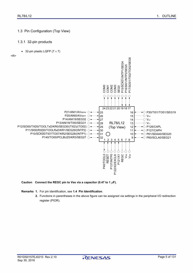
1.3 Pin Configuration (Top View)
1.3.1 32-pin products
• 32-pin plastic LQFP (7 × 7)
161514131211109
2526272829303132
24 23 22 21 20 19 18 17
1 2 3 4 5 6 7 8
P21/ANI1/AVREFM
P20/ANI0/AVREFP
P14/ANI19/SEG32P13/ANI18/TI00/SEG31
P12/SO00/TXD0/TOOLTxD/KR0/SEG30/(TI02)/(TO02)P11/SI00/RXD0/TOOLRxD/KR1/SEG29/(INTP2)
P10/SCK00/TI07/TO07/KR2/SEG28/(INTP1)P140/TO00/PCLBUZ0/KR3/SEG27
P30/TI01/TO01/SEG19VL4
VL2
VL1
P126/CAPLP127/CAPHP61/SDAA0/SEG20P60/SCLA0/SEG21
CO
M0
CO
M1
CO
M2
CO
M3
SE
G0
P1
5/S
CK
01
/IN
TP
1/S
EG
4P
16
/SI0
1/I
NT
P2
/SE
G5
P1
7/S
O0
1/T
I02
/TO
02
/SE
G6
P4
0/T
OO
L0
RE
SE
TP
13
7/I
NT
P0
P1
22
/X2
/EX
CL
KP
12
1/X
1R
EG
CV
SS
VD
D
RL78/L12(Top View)
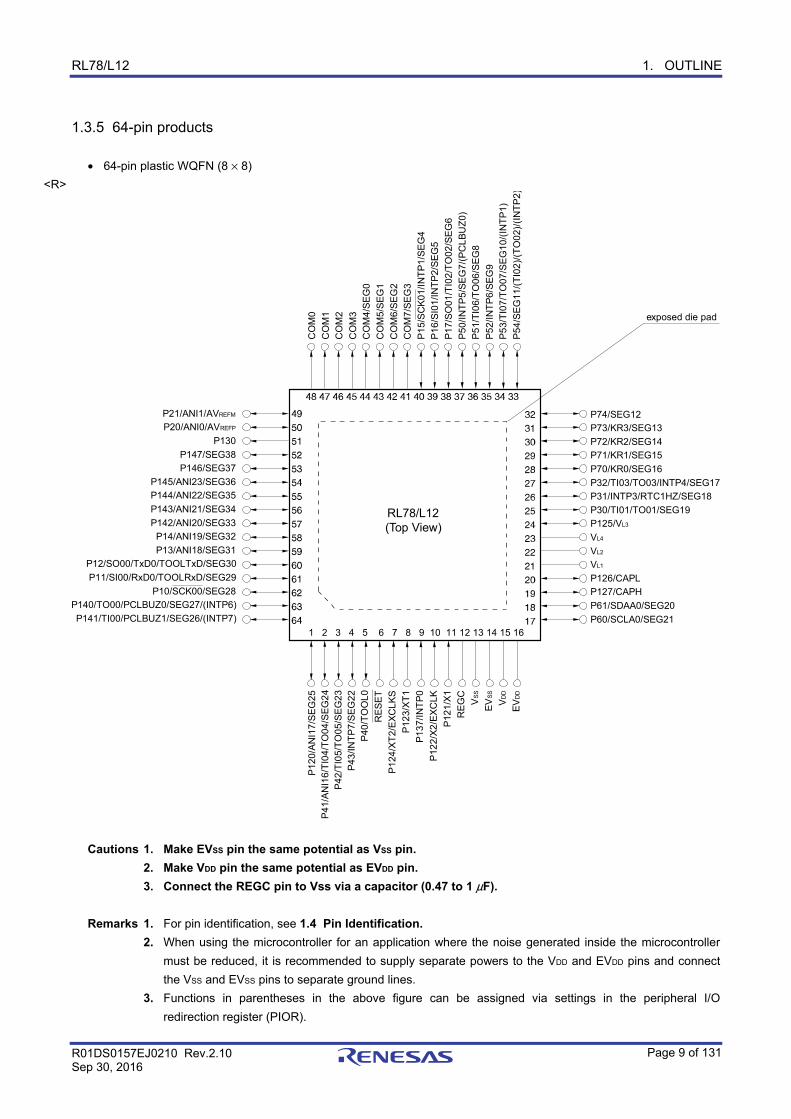
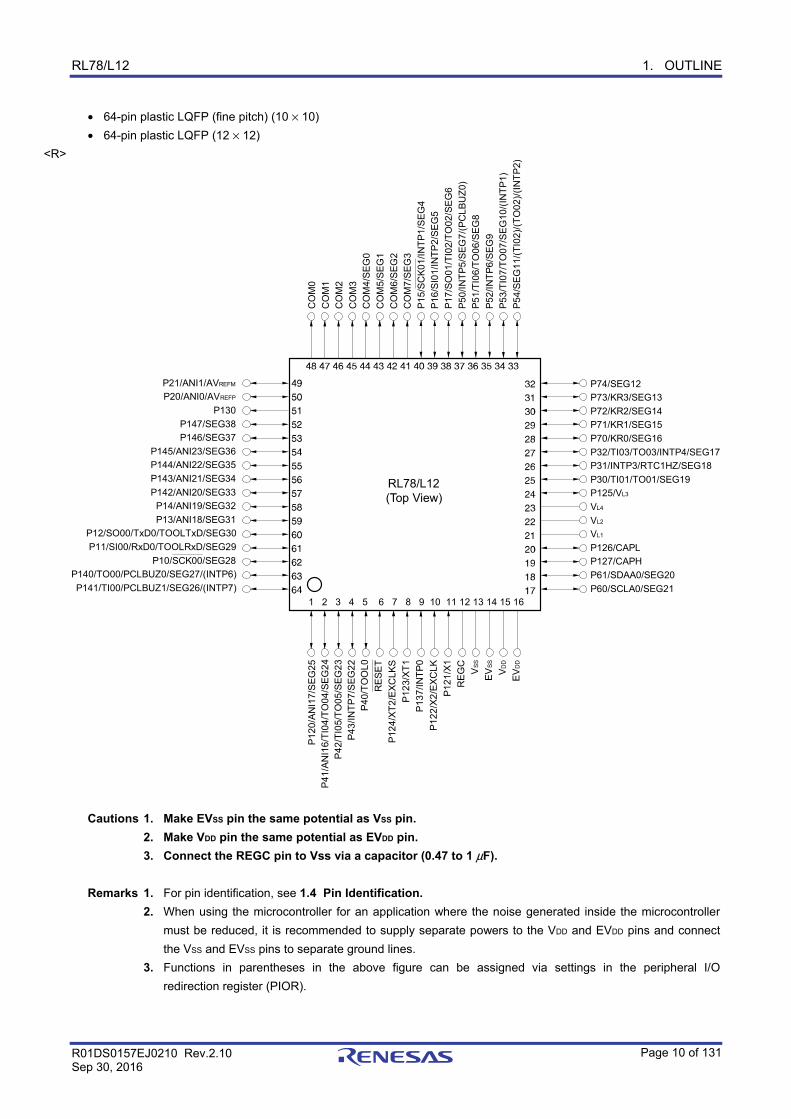
Caution Connect the REGC pin to Vss via a capacitor (0.47 to 1 μF).
Remarks 1. For pin identification, see 1.4 Pin Identification.
2. Functions in parentheses in the above figure can be assigned via settings in the peripheral I/O redirection
register (PIOR).
<R>
RL78/L12 1. OUTLINE
R01DS0157EJ0210 Rev.2.10 Sep 30, 2016
Page 6 of 131
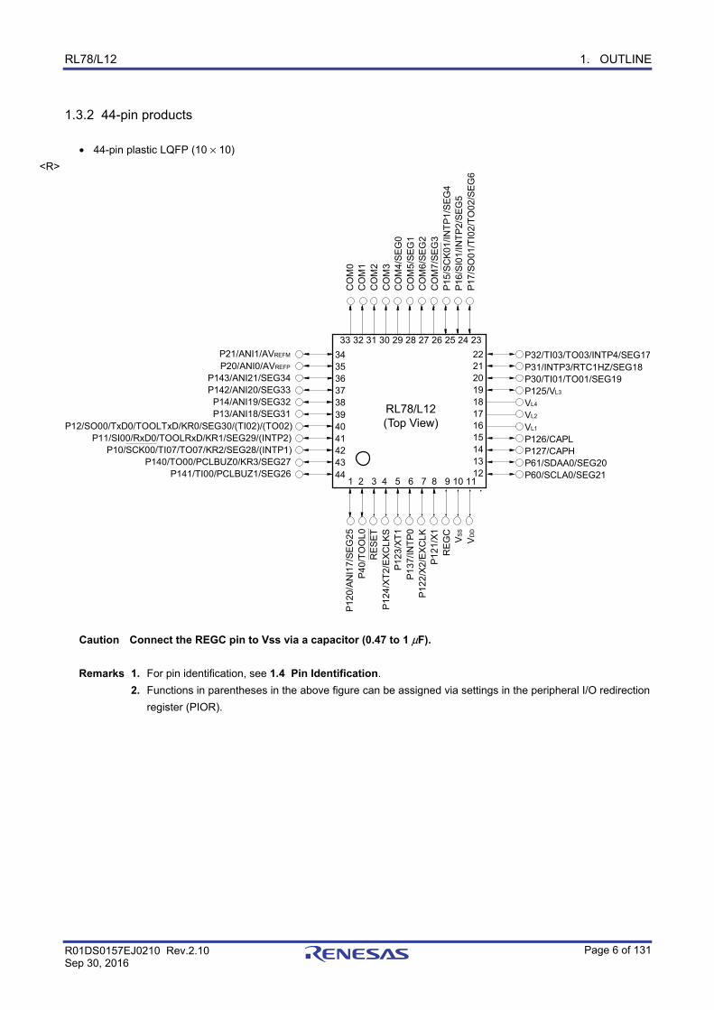
1.3.2 44-pin products
• 44-pin plastic LQFP (10 × 10)
33 32 31 30 29 28 27 26 25 24 23
1 2 3 4 5 6 7 8 9 10 11
3435363738394041424344
2221201918171615141312
P21/ANI1/AVREFM
P20/ANI0/AVREFP
P143/ANI21/SEG34P142/ANI20/SEG33
P14/ANI19/SEG32P13/ANI18/SEG31
P12/SO00/TxD0/TOOLTxD/KR0/SEG30/(TI02)/(TO02)P11/SI00/RxD0/TOOLRxD/KR1/SEG29/(INTP2)
P10/SCK00/TI07/TO07/KR2/SEG28/(INTP1)P140/TO00/PCLBUZ0/KR3/SEG27
P141/TI00/PCLBUZ1/SEG26
CO
M0
CO
M1
CO
M2
CO
M3
CO
M4
/SE
G0
CO
M5
/SE
G1
CO
M6
/SE
G2
CO
M7
/SE
G3
P15
/SC
K01
/IN
TP
1/S
EG
4P
16/S
I01
/INT
P2
/SE
G5
P17
/SO
01/
TI0
2/T
O0
2/S
EG
6
P1
20/
AN
I17
/SE
G2
5P
40
/TO
OL
0R
ES
ET
P1
24
/XT
2/E
XC
LK
SP
12
3/X
T1
P1
37/
INT
P0
P1
22
/X2
/EX
CL
KP
12
1/X
1R
EG
CV
SS
VD
D
P32/TI03/TO03/INTP4/SEG17P31/INTP3/RTC1HZ/SEG18P30/TI01/TO01/SEG19P125/VL3
VL4
VL2
VL1
P126/CAPLP127/CAPHP61/SDAA0/SEG20P60/SCLA0/SEG21
RL78/L12(Top View)
Caution Connect the REGC pin to Vss via a capacitor (0.47 to 1 μF).
Remarks 1. For pin identification, see 1.4 Pin Identification.
2. Functions in parentheses in the above figure can be assigned via settings in the peripheral I/O redirection
register (PIOR).
<R>
RL78/L12 1. OUTLINE
R01DS0157EJ0210 Rev.2.10 Sep 30, 2016
Page 7 of 131
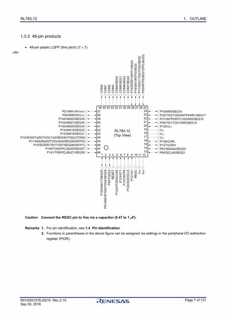
1.3.3 48-pin products
• 48-pin plastic LQFP (fine pitch) (7 × 7)
36 35 34 33 32 31 30 29 28 27 26 25
1 2 3 4 5 6 7 8 9 10 11 12
373839404142434445464748
242322212019181716151413
P21/ANI1/AVREFM
P20/ANI0/AVREFP
P144/ANI22/SEG35P143/ANI21/SEG34P142/ANI20/SEG33
P14/ANI19/SEG32P13/ANI18/SEG31
P12/SO00/TxD0/TOOLTxD/SEG30/(TI02)/(TO02)P11/SI00/RxD0/TOOLRxD/SEG29/(INTP2)
P10/SCK00/TI07/TO07/SEG28/(INTP1)P140/TO00/PCLBUZ0/SEG27P141/TI00/PCLBUZ1/SEG26
CO
M0
CO
M1
CO
M2
CO
M3
CO
M4
/SE
G0
CO
M5
/SE
G1
CO
M6
/SE
G2
CO
M7
/SE
G3
P1
5/S
CK
01
/IN
TP
1/S
EG
4P
16/
SI0
1/IN
TP
2/S
EG
5P
17/
SO
01/T
I02
/TO
02
/SE
G6
P5
0/IN
TP
5/S
EG
7/(
PC
LBU
Z0)
P70/KR0/SEG16P32/TI03/TO03/INTP4/KR1/SEG17P31/INTP3/RTC1HZ/KR2/SEG18P30/TI01/TO01/KR3/SEG19P125/VL3
VL4
VL2
VL1
P126/CAPLP127/CAPHP61/SDAA0/SEG20P60/SCLA0/SEG21
P1
20
/AN
I17
/SE
G2
5P
41
/AN
I16
/TI0
4/T
O04
/SE
G2
4P
40/T
OO
L0
RE
SE
TP
12
4/X
T2
/EX
CL
KS
P1
23
/XT
1P
13
7/I
NT
P0
P12
2/X
2/E
XC
LK
P1
21/
X1
RE
GC
VS
S
VD
D
RL78/L12(Top View)
Caution Connect the REGC pin to Vss via a capacitor (0.47 to 1 μF).
Remarks 1. For pin identification, see 1.4 Pin Identification.
2. Functions in parentheses in the above figure can be assigned via settings in the peripheral I/O redirection
register (PIOR).
<R>
RL78/L12 1. OUTLINE
R01DS0157EJ0210 Rev.2.10 Sep 30, 2016
Page 8 of 131
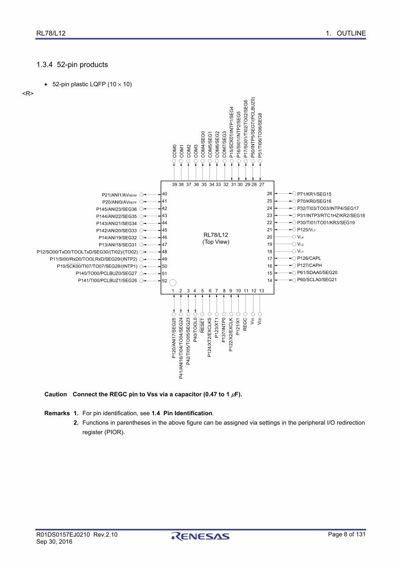
1.3.4 52-pin products
• 52-pin plastic LQFP (10 × 10)
1 2 3 4 5 6 7 8 9 10 11 12 13
39 38 37 36 35 34 33 32 31 30 29 28 27
P21/ANI1/AVREFM
P20/ANI0/AVREFP
P145/ANI23/SEG36
P144/ANI22/SEG35
P143/ANI21/SEG34
P142/ANI20/SEG33
P14/ANI19/SEG32
P13/ANI18/SEG31
P12/SO00/TxD0/TOOLTxD/SEG30/(TI02)/(TO02)
P11/SI00/RxD0/TOOLRxD/SEG29/(INTP2)
P10/SCK00/TI07/TO07/SEG28/(INTP1)
P140/TO00/PCLBUZ0/SEG27
P141/TI00/PCLBUZ1/SEG26
P1
20
/AN
I17
/SE
G2
5
P4
1/A
NI1
6/T
I04
/TO
04
/SE
G2
4
P4
2/T
I05
/TO
05
/SE
G2
3
P4
0/T
OO
L0
RE
SE
T
P1
24
/XT
2/E
XC
LK
S
P1
23
/XT
1
P1
37
/IN
TP
0
P1
22
/X2
/EX
CL
K
P1
21
/X1
RE
GC
VS
S
VD
D
CO
M0
CO
M1
CO
M2
CO
M3
CO
M4
/SE
G0
CO
M5
/SE
G1
CO
M6
/SE
G2
CO
M7
/SE
G3
P1
5/S
CK
01
/IN
TP
1/S
EG
4
P1
6/S
I01
/IN
TP
2/S
EG
5
P1
7/S
O0
1/T
I02
/TO
02
/SE
G6
P5
0/I
NT
P5
/SE
G7
/(P
CL
BU
Z0
)
P5
1/T
I06
/TO
06
/SE
G8
P71/KR1/SEG15
P70/KR0/SEG16
P32/TI03/TO03/INTP4/SEG17
P31/INTP3/RTC1HZ/KR2/SEG18
P30/TI01/TO01/KR3/SEG19
P125/VL3
VL4
VL2
VL1
P126/CAPL
P127/CAPH
P61/SDAA0/SEG20
P60/SCLA0/SEG21
26
25
24
23
22
21
20
19
18
17
16
15
14
40
41
42
43
44
45
46
47
48
49
50
51
52
RL78/L12(Top View)
Caution Connect the REGC pin to Vss via a capacitor (0.47 to 1 μF).
Remarks 1. For pin identification, see 1.4 Pin Identification.
2. Functions in parentheses in the above figure can be assigned via settings in the peripheral I/O redirection
register (PIOR).
<R>
RL78/L12 1. OUTLINE
R01DS0157EJ0210 Rev.2.10 Sep 30, 2016
Page 9 of 131
1.3.5 64-pin products
• 64-pin plastic WQFN (8 × 8)
1 2 3 4 5 6 7 8 9 10 11 12 13 14 15 16
P21/ANI1/AVREFM
P20/ANI0/AVREFP
P130
P147/SEG38
P146/SEG37
P145/ANI23/SEG36
P144/ANI22/SEG35
P143/ANI21/SEG34
P142/ANI20/SEG33
P14/ANI19/SEG32
P13/ANI18/SEG31
P12/SO00/TxD0/TOOLTxD/SEG30
P11/SI00/RxD0/TOOLRxD/SEG29
P10/SCK00/SEG28
P140/TO00/PCLBUZ0/SEG27/(INTP6)
P141/TI00/PCLBUZ1/SEG26/(INTP7)
P74/SEG12
P73/KR3/SEG13
P72/KR2/SEG14
P71/KR1/SEG15
P70/KR0/SEG16
P32/TI03/TO03/INTP4/SEG17
P31/INTP3/RTC1HZ/SEG18
P30/TI01/TO01/SEG19
P125/VL3
VL4
VL2
VL1
P126/CAPL
P127/CAPH
P61/SDAA0/SEG20
P60/SCLA0/SEG21
CO
M0
CO
M1
CO
M2
CO
M3
CO
M4
/SE
G0
CO
M5
/SE
G1
CO
M6
/SE
G2
CO
M7
/SE
G3
P1
5/S
CK
01/
INT
P1
/SE
G4
P1
6/S
I01
/IN
TP
2/S
EG
5
P1
7/S
O0
1/T
I02
/TO
02
/SE
G6
P5
0/I
NT
P5
/SE
G7
/(P
CL
BU
Z0
)
P5
1/T
I06/
TO
06/S
EG
8
P5
2/I
NT
P6
/SE
G9
P5
3/T
I07/
TO
07/S
EG
10
/(IN
TP
1)
P5
4/S
EG
11
/(T
I02
)/(T
O0
2)/
(IN
TP
2)
P12
0/A
NI1
7/S
EG
25P
41
/AN
I16
/TI0
4/T
O0
4/S
EG
24
P4
2/T
I05/
TO
05/
SE
G2
3P
43/I
NT
P7/
SE
G22
P40
/TO
OL
0
RE
SE
T
P1
24/X
T2
/EX
CLK
S
P12
3/X
T1
P13
7/I
NT
P0
P12
2/X
2/E
XC
LK
P1
21/X
1
RE
GC
VS
S
EV
SS
VD
D
EV
DD
exposed die pad
RL78/L12(Top View)
Cautions 1. Make EVSS pin the same potential as VSS pin. 2. Make VDD pin the same potential as EVDD pin. 3. Connect the REGC pin to Vss via a capacitor (0.47 to 1 μF). Remarks 1. For pin identification, see 1.4 Pin Identification. 2. When using the microcontroller for an application where the noise generated inside the microcontroller
must be reduced, it is recommended to supply separate powers to the VDD and EVDD pins and connect
the VSS and EVSS pins to separate ground lines.
3. Functions in parentheses in the above figure can be assigned via settings in the peripheral I/O
redirection register (PIOR).
<R>
RL78/L12 1. OUTLINE
R01DS0157EJ0210 Rev.2.10 Sep 30, 2016
Page 10 of 131
• 64-pin plastic LQFP (fine pitch) (10 × 10)
• 64-pin plastic LQFP (12 × 12)
1 2 3 4 5 6 7 8 9 10 11 12 13 14 15 16
P21/ANI1/AVREFM
P20/ANI0/AVREFP
P130
P147/SEG38
P146/SEG37
P145/ANI23/SEG36
P144/ANI22/SEG35
P143/ANI21/SEG34
P142/ANI20/SEG33
P14/ANI19/SEG32
P13/ANI18/SEG31
P12/SO00/TxD0/TOOLTxD/SEG30
P11/SI00/RxD0/TOOLRxD/SEG29
P10/SCK00/SEG28
P140/TO00/PCLBUZ0/SEG27/(INTP6)
P141/TI00/PCLBUZ1/SEG26/(INTP7)
P74/SEG12
P73/KR3/SEG13
P72/KR2/SEG14
P71/KR1/SEG15
P70/KR0/SEG16
P32/TI03/TO03/INTP4/SEG17
P31/INTP3/RTC1HZ/SEG18
P30/TI01/TO01/SEG19
P125/VL3
VL4
VL2
VL1
P126/CAPL
P127/CAPH
P61/SDAA0/SEG20
P60/SCLA0/SEG21
CO
M0
CO
M1
CO
M2
CO
M3
CO
M4
/SE
G0
CO
M5
/SE
G1
CO
M6
/SE
G2
CO
M7
/SE
G3
P1
5/S
CK
01
/IN
TP
1/S
EG
4
P1
6/S
I01/
INT
P2
/SE
G5
P1
7/S
O0
1/T
I02
/TO
02/S
EG
6
P5
0/I
NT
P5
/SE
G7
/(P
CL
BU
Z0)
P5
1/T
I06/
TO
06/
SE
G8
P5
2/I
NT
P6
/SE
G9
P5
3/T
I07/
TO
07
/SE
G1
0/(
INT
P1
)
P5
4/S
EG
11/(
TI0
2)/(
TO
02
)/(I
NT
P2
)
P12
0/A
NI1
7/S
EG
25P
41
/AN
I16
/TI0
4/T
O0
4/S
EG
24
P4
2/T
I05/
TO
05/S
EG
23
P43
/IN
TP
7/S
EG
22P
40/T
OO
L0
RE
SE
T
P12
4/X
T2
/EX
CLK
S
P12
3/X
T1
P13
7/I
NT
P0
P12
2/X
2/E
XC
LK
P12
1/X
1
RE
GC
VS
S
EV
SS
VD
D
EV
DD
RL78/L12(Top View)
Cautions 1. Make EVSS pin the same potential as VSS pin. 2. Make VDD pin the same potential as EVDD pin. 3. Connect the REGC pin to Vss via a capacitor (0.47 to 1 μF). Remarks 1. For pin identification, see 1.4 Pin Identification. 2. When using the microcontroller for an application where the noise generated inside the microcontroller
must be reduced, it is recommended to supply separate powers to the VDD and EVDD pins and connect
the VSS and EVSS pins to separate ground lines.
3. Functions in parentheses in the above figure can be assigned via settings in the peripheral I/O
redirection register (PIOR).
<R>
RL78/L12 1. OUTLINE
R01DS0157EJ0210 Rev.2.10 Sep 30, 2016
Page 11 of 131
1.4 Pin Identification
ANI0, ANI1,
ANI16 to ANI23: Analog Input
AVREFM: Analog Reference
Voltage Minus
AVREFP: Analog Reference
Voltage Plus
CAPH, CAPL: Capacitor for LCD
COM0 to COM7,
EVDD: Power Supply for Port
EVSS: Ground for Port
EXCLK: External Clock Input
(Main System Clock)
EXCLKS: External Clock Input
(Subsystem Clock)
INTP0 to INTP7: Interrupt Request From
Peripheral
KR0 to KR3: Key Return
P10 to P17: Port 1
P20, P21: Port 2
P30 to P32: Port 3
P40 to P43: Port 4
P50 to P54: Port 5
P60, P61: Port 6
P70 to P74: Port 7
P120 to P127: Port 12
P130, P137: Port 13
P140 to P147: Port 14
PCLBUZ0, PCLBUZ1: Programmable Clock
Output/Buzzer Output
REGC: Regulator Capacitance
RESET: Reset
RTC1HZ: Real-time Clock Correction Clock
(1 Hz) Output
RxD0: Receive Data
SCK00, SCK01: Serial Clock Input/Output
SCLA0: Serial Clock Input/Output
SDAA0: Serial Data Input/Output
SEG0 to SEG38: LCD Segment Output
SI00, SI01: Serial Data Input
SO00, SO01: Serial Data Output
TI00 to TI07: Timer Input
TO00 to TO07: Timer Output
TOOL0: Data Input/Output for Tool
TOOLRxD, TOOLTxD: Data Input/Output for External Device
TxD0: Transmit Data
VDD: Power Supply
VL1 to VL4: LCD Power Supply
VSS: Ground
X1, X2: Crystal Oscillator (Main System Clock)
XT1, XT2: Crystal Oscillator (Subsystem Clock)
RL78/L12 1. OUTLINE
R01DS0157EJ0210 Rev.2.10 Sep 30, 2016
Page 12 of 131
1.5 Block Diagram
1.5.1 32-pin products
ch2
ch3
ch0
ch1
ch4
ch5
ch6
ch7
PORT 2 P20, P212
PORT 3 P30
PORT 1 P10 to P178
PORT 4 P40
VOLTAGEREGULATOR REGC
INTERRUPTCONTROL
RAM
POWER ON RESET/VOLTAGE DETECTOR
POR/LVDCONTROL
RESET CONTROL
SYSTEMCONTROL
RESETX1/P121X2/EXCLK/P122HIGH-SPEED
ON-CHIPOSCILLATOR
ON-CHIP DEBUG TOOL0/P40
TIMER ARRAY UNIT0 (8ch)
TI02/TO02/P17(TI02/TO02/P12)
2
INTP0/P137
INTP1/P15(INTP1/P10),INTP2/P16(INTP2/P11)
TO00/P140TI00/P13
BCD ADJUSTMENT
VSS TOOLRxD/P11, TOOLTxD/P12
VDD
SERIAL ARRAY UNIT0 (2ch)
UART0RxD0/P11TxD0/P12
CSI01SCK01/P15
SO01/P17SI01/P16
SCK00/P10
SO00/P12SI00/P11 CSI00
SCLA0/P60
SERIALINTERFACE IICA0
SDAA0/P61
MULTIPLIER&DIVIDER,
MULITIPLY-ACCUMULATOR
KEY RETURN3 KR0/P12 to KR2/P10
DIRECT MEMORYACCESS CONTROL
PORT 6 P60, P612
BUZZER OUTPUT
PCLBUZ0/P140CLOCK OUTPUTCONTROL
TI01/TO01/P30
A/D CONVERTER
2 ANI0/P20, ANI1/P21
AVREFP/P20AVREFM/P21
2 ANI18/P13, ANI19/P14
PORT 13 P137
WINDOWWATCHDOG
TIMER
RL78CPU
CORE
CODE FLASH MEMORY
DATA FLASH MEMORY
PORT 12P121, P1222
P126, P1272
LCDCONTROLLER/
DRIVERCOM0 to COM3
13SEG0, SEG4 to SEG6,
SEG19 to SEG21,SEG27 to SEG32
4
VL1, VL2, VL4
CAPHCAPL
RAM SPACEFOR LCD DATA
TI07/TO07/P10
KR3/P140
PORT 14 P140
REAL-TIMECLOCK
LOW-SPEEDON-CHIP
OSCILLATOR
12- BIT INTERVALTIMER
CRC
Remark Functions in parentheses in the above figure can be assigned via settings in the peripheral I/O redirection
register (PIOR)
RL78/L12 1. OUTLINE
R01DS0157EJ0210 Rev.2.10 Sep 30, 2016
Page 13 of 131
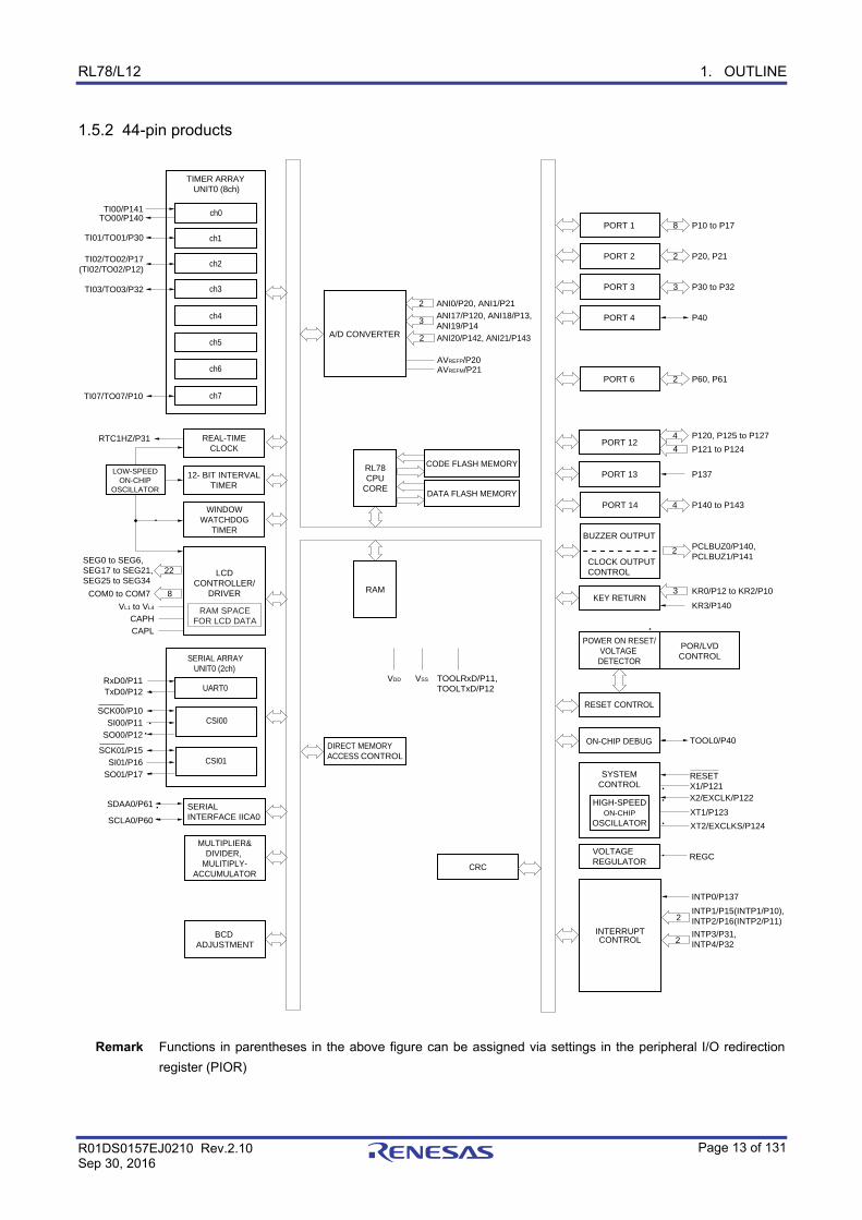
1.5.2 44-pin products
ch2
ch3
ch0
ch1
ch4
ch5
ch6
ch7
PORT 2 P20, P212
PORT 3 P30 to P323
PORT 1 P10 to P178
PORT 4 P40
VOLTAGEREGULATOR REGC
INTERRUPTCONTROL
RAM
POWER ON RESET/VOLTAGE DETECTOR
POR/LVDCONTROL
RESET CONTROL
SYSTEMCONTROL
RESETX1/P121X2/EXCLK/P122HIGH-SPEED
ON-CHIPOSCILLATOR
ON-CHIP DEBUG TOOL0/P40
TIMER ARRAY UNIT0 (8ch)
TI02/TO02/P17(TI02/TO02/P12)
TI03/TO03/P32
2
INTP0/P137
INTP3/P31,INTP4/P32
INTP1/P15(INTP1/P10),INTP2/P16(INTP2/P11)
BCD ADJUSTMENT
VSS TOOLRxD/P11, TOOLTxD/P12
VDD
2
SERIAL ARRAY UNIT0 (2ch)
UART0RxD0/P11TxD0/P12
CSI01SCK01/P15
SO01/P17SI01/P16
SCK00/P10
SO00/P12SI00/P11 CSI00
SCLA0/P60
SERIALINTERFACE IICA0
SDAA0/P61
MULTIPLIER&DIVIDER,
MULITIPLY-ACCUMULATOR
XT1/P123
XT2/EXCLKS/P124
KEY RETURN3 KR0/P12 to KR2/P10
DIRECT MEMORYACCESS CONTROL
PORT 6 P60, P612
BUZZER OUTPUTPCLBUZ0/P140, PCLBUZ1/P141
CLOCK OUTPUTCONTROL
2
TI01/TO01/P30
A/D CONVERTER
2 ANI0/P20, ANI1/P21
AVREFP/P20AVREFM/P21
2 ANI20/P142, ANI21/P143
3ANI17/P120, ANI18/P13,ANI19/P14
PORT 13 P137
PORT 14 P140 to P1434WINDOWWATCHDOG
TIMER
RTC1HZ/P31 REAL-TIMECLOCK
RL78CPU
CORE
CODE FLASH MEMORY
DATA FLASH MEMORY
PORT 12P121 to P1244
P120, P125 to P1274
LCDCONTROLLER/
DRIVERCOM0 to COM7
22SEG0 to SEG6, SEG17 to SEG21,SEG25 to SEG34
8
VL1 to VL4
CAPHCAPL
RAM SPACEFOR LCD DATA
TI07/TO07/P10
KR3/P140
TO00/P140TI00/P141
CRC
LOW-SPEEDON-CHIP
OSCILLATOR
12- BIT INTERVALTIMER
Remark Functions in parentheses in the above figure can be assigned via settings in the peripheral I/O redirection
register (PIOR)
RL78/L12 1. OUTLINE
R01DS0157EJ0210 Rev.2.10 Sep 30, 2016
Page 14 of 131
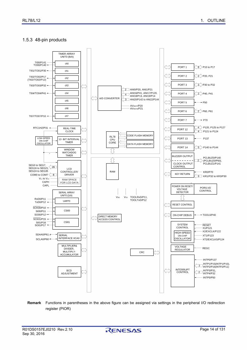
1.5.3 48-pin products
ch2
ch3
ch0
ch1
ch4
ch5
ch6
ch7
PORT 2 P20, P212
PORT 3 P30 to P323
PORT 1 P10 to P178
PORT 4 P40, P412
PORT 5 P50
VOLTAGEREGULATOR REGC
INTERRUPTCONTROL
RAM
POWER ON RESET/VOLTAGE DETECTOR
POR/LVDCONTROL
RESET CONTROL
SYSTEMCONTROL
RESETX1/P121X2/EXCLK/P122HIGH-SPEED
ON-CHIPOSCILLATOR
ON-CHIP DEBUG TOOL0/P40
TIMER ARRAY UNIT0 (8ch)
TI02/TO02/P17(TI02/TO02/P12)
TI03/TO03/P32
TI04/TO04/P41
2
INTP0/P137
INTP3/P31,INTP4/P32
INTP1/P15(INTP1/P10),INTP2/P16(INTP2/P11)
BCD ADJUSTMENT
VSS TOOLRxD/P11, TOOLTxD/P12
VDD
2
INTP5/P50
SERIAL ARRAY UNIT0 (2ch)
UART0RxD0/P11TxD0/P12
CSI01SCK01/P15
SO01/P17SI01/P16
SCK00/P10
SO00/P12SI00/P11 CSI00
SCLA0/P60
SERIALINTERFACE IICA0
SDAA0/P61
MULTIPLIER&DIVIDER,
MULITIPLY-ACCUMULATOR
XT1/P123
XT2/EXCLKS/P124
KEY RETURNKR0/P70
DIRECT MEMORYACCESS CONTROL
PORT 7 P70
PORT 6 P60, P612
BUZZER OUTPUTPCLBUZ0/P140(PCLBUZ0/P50), PCLBUZ1/P141CLOCK OUTPUT
CONTROL
2
TI01/TO01/P30
A/D CONVERTER
2 ANI0/P20, ANI1/P21
AVREFP/P20AVREFM/P21
3 ANI20/P142 to ANI22/P144
4ANI16/P41, ANI17/P120,ANI18/P13, ANI19/P14
PORT 13 P137
PORT 14 P140 to P1445WINDOW
WATCHDOGTIMER
RTC1HZ/P31 REAL-TIMECLOCK
RL78CPU
CORE
CODE FLASH MEMORY
DATA FLASH MEMORY
PORT 12P121 to P1244
P120, P125 to P1274
LCDCONTROLLER/
DRIVERCOM0 to COM7
26SEG0 to SEG7, SEG16 to SEG21,SEG24 to SEG35
8
VL1 to VL4
CAPHCAPL
RAM SPACEFOR LCD DATA
TI07/TO07/P10
KR1/P32 to KR3/P303
TO00/P140TI00/P141
LOW-SPEEDON-CHIP
OSCILLATOR
12- BIT INTERVALTIMER
CRC
Remark Functions in parentheses in the above figure can be assigned via settings in the peripheral I/O redirection
register (PIOR)
RL78/L12 1. OUTLINE
R01DS0157EJ0210 Rev.2.10 Sep 30, 2016
Page 15 of 131
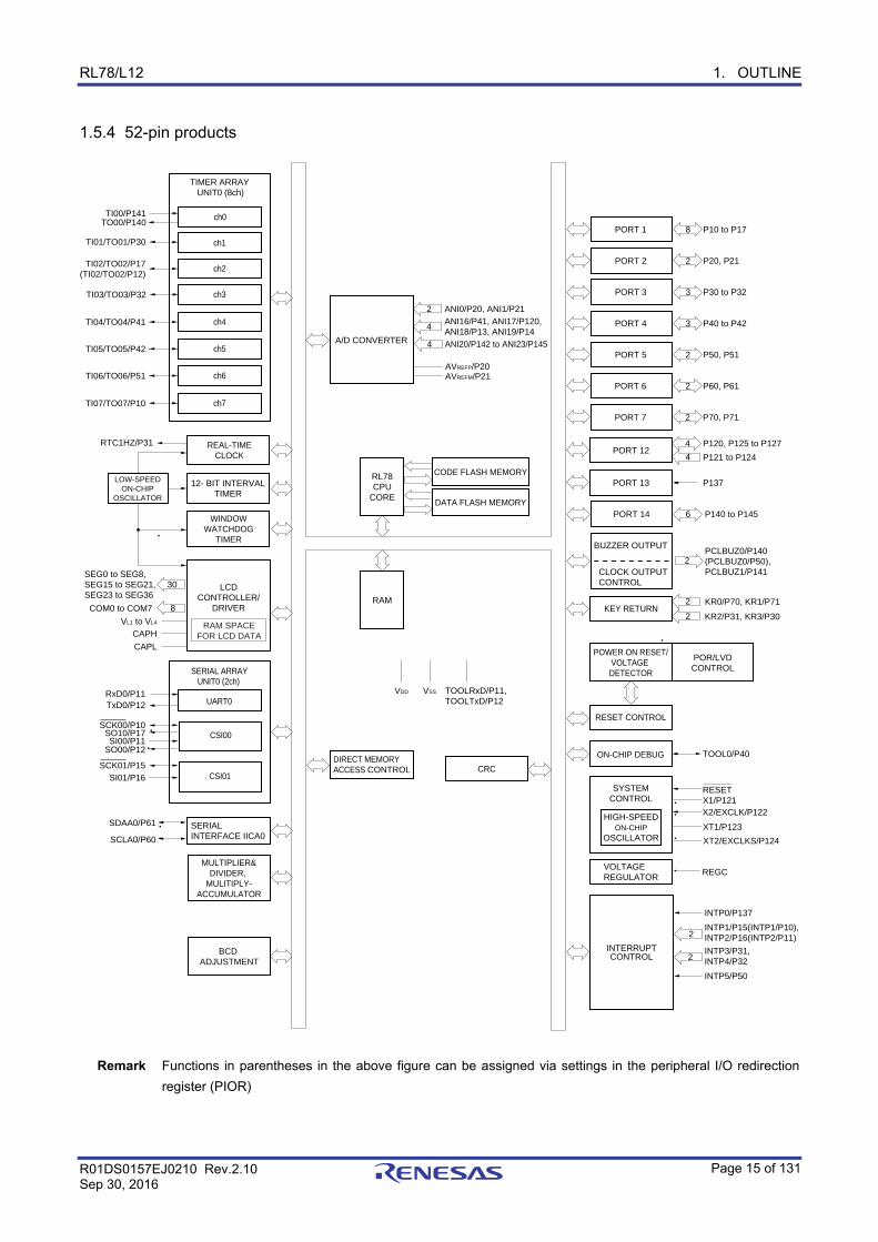
1.5.4 52-pin products
PORT 2 P20, P212
PORT 3 P30 to P323
PORT 1 P10 to P178
PORT 4 P40 to P423
PORT 5 P50, P512
VOLTAGEREGULATOR REGC
INTERRUPTCONTROL
RAM
POWER ON RESET/VOLTAGE DETECTOR
POR/LVDCONTROL
RESET CONTROL
SYSTEMCONTROL
RESETX1/P121X2/EXCLK/P122HIGH-SPEED
ON-CHIPOSCILLATOR
ON-CHIP DEBUG TOOL0/P40
TIMER ARRAY UNIT0 (8ch)
ch2TI02/TO02/P17(TI02/TO02/P12)
ch3TI03/TO03/P32
ch0
ch1
ch4TI04/TO04/P41
ch5TI05/TO05/P42
ch6TI06/TO06/P51
ch7
2
INTP0/P137
INTP3/P31,INTP4/P32
INTP1/P15(INTP1/P10),INTP2/P16(INTP2/P11)
SO10/P17
BCD ADJUSTMENT
SERIAL ARRAY UNIT0 (2ch)
UART0RxD0/P11TxD0/P12
CSI01SCK01/P15
SI01/P16
SCK00/P10
SO00/P12SI00/P11
CSI00
VSS TOOLRxD/P11, TOOLTxD/P12
VDD
SCLA0/P60
SERIALINTERFACE IICA0
SDAA0/P61
2
INTP5/P50
MULTIPLIER&DIVIDER,
MULITIPLY-ACCUMULATOR
XT1/P123
XT2/EXCLKS/P124
KEY RETURN2 KR0/P70, KR1/P71
DIRECT MEMORYACCESS CONTROL
PORT 7 P70, P712
PORT 6 P60, P612
BUZZER OUTPUTPCLBUZ0/P140(PCLBUZ0/P50), PCLBUZ1/P141CLOCK OUTPUT
CONTROL
2
TI01/TO01/P30
A/D CONVERTER
2 ANI0/P20, ANI1/P21
AVREFP/P20AVREFM/P21
4 ANI20/P142 to ANI23/P145
4ANI16/P41, ANI17/P120,ANI18/P13, ANI19/P14
PORT 13 P137
PORT 14 P140 to P1456WINDOWWATCHDOG
TIMER
RTC1HZ/P31 REAL-TIMECLOCK
RL78CPU
CORE
CODE FLASH MEMORY
DATA FLASH MEMORY
PORT 12P121 to P1244
P120, P125 to P1274
CAPL
LCDCONTROLLER/
DRIVERCOM0 to COM7
30SEG0 to SEG8, SEG15 to SEG21,SEG23 to SEG36
8
VL1 to VL4
CAPHRAM SPACE
FOR LCD DATA
TI07/TO07/P10
KR2/P31, KR3/P302
TO00/P140TI00/P141
CRC
LOW-SPEEDON-CHIP
OSCILLATOR
12- BIT INTERVALTIMER
Remark Functions in parentheses in the above figure can be assigned via settings in the peripheral I/O redirection
register (PIOR)
RL78/L12 1. OUTLINE
R01DS0157EJ0210 Rev.2.10 Sep 30, 2016
Page 16 of 131
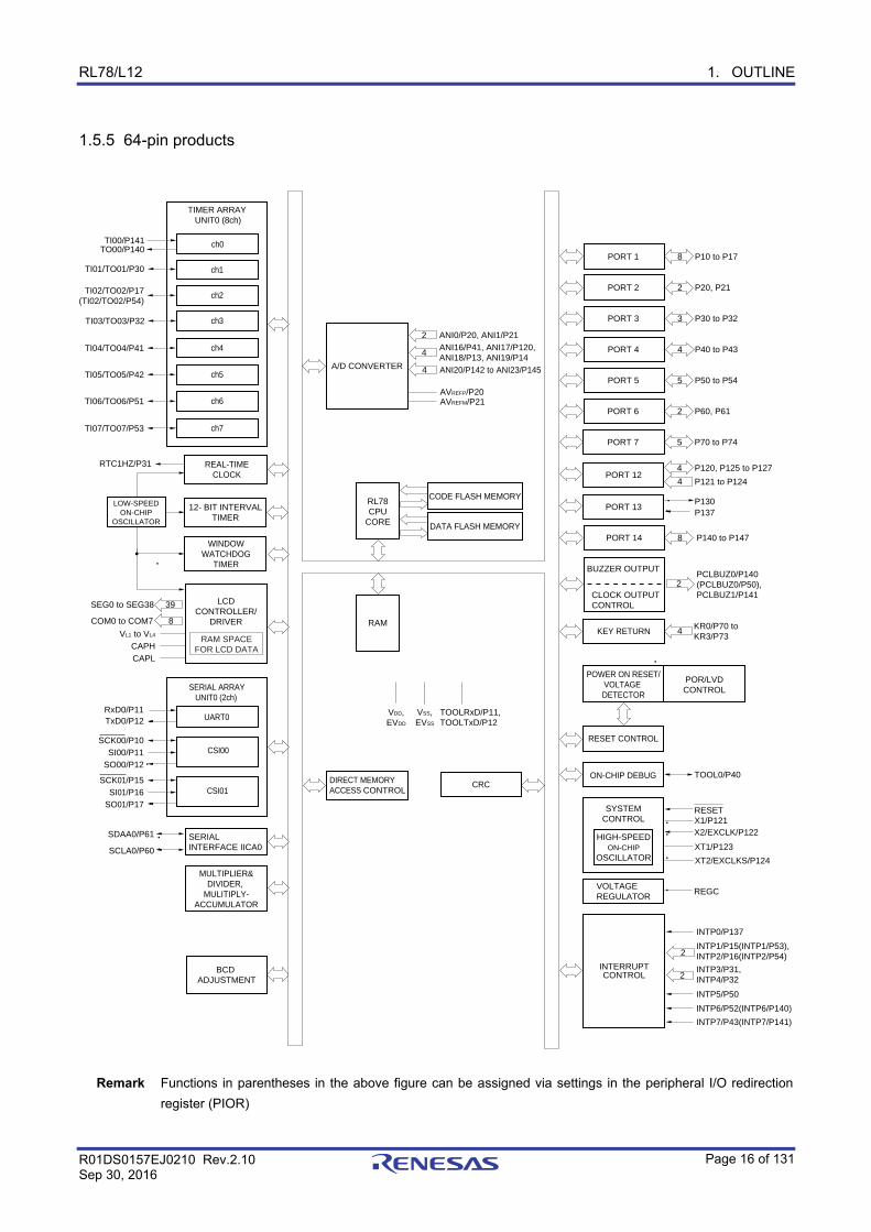
1.5.5 64-pin products
PORT 2 P20, P212
PORT 3 P30 to P323
PORT 1 P10 to P178
PORT 4 P40 to P434
PORT 5 P50 to P545
VOLTAGEREGULATOR REGC
INTERRUPTCONTROL
RAM
POWER ON RESET/VOLTAGE DETECTOR
POR/LVDCONTROL
RESET CONTROL
SYSTEMCONTROL
RESETX1/P121X2/EXCLK/P122HIGH-SPEED
ON-CHIPOSCILLATOR
ON-CHIP DEBUG TOOL0/P40
TIMER ARRAY UNIT0 (8ch)
ch2TI02/TO02/P17(TI02/TO02/P54)
ch3TI03/TO03/P32
ch0
ch1
ch4TI04/TO04/P41
ch5TI05/TO05/P42
ch6TI06/TO06/P51
ch7
2
INTP0/P137
INTP3/P31,INTP4/P32
INTP6/P52(INTP6/P140)
INTP1/P15(INTP1/P53),INTP2/P16(INTP2/P54)
BCD ADJUSTMENT
SERIAL ARRAY UNIT0 (2ch)
UART0RxD0/P11TxD0/P12
CSI01SCK01/P15
SO01/P17SI01/P16
SCK00/P10
SO00/P12SI00/P11 CSI00
VSS,EVSS
TOOLRxD/P11, TOOLTxD/P12
VDD,EVDD
SCLA0/P60
SERIALINTERFACE IICA0
SDAA0/P61
2
INTP5/P50
MULTIPLIER&DIVIDER,
MULITIPLY-ACCUMULATOR
XT1/P123
XT2/EXCLKS/P124
KEY RETURN 4 KR0/P70 to KR3/P73
DIRECT MEMORYACCESS CONTROL
PORT 7 P70 to P745
PORT 6 P60, P612
BUZZER OUTPUTPCLBUZ0/P140(PCLBUZ0/P50), PCLBUZ1/P141CLOCK OUTPUT
CONTROL
2
TI01/TO01/P30
A/D CONVERTER
2 ANI0/P20, ANI1/P21
AVREFP/P20AVREFM/P21
4 ANI20/P142 to ANI23/P145
4ANI16/P41, ANI17/P120,ANI18/P13, ANI19/P14
PORT 13P130P137
PORT 14 P140 to P1478WINDOW
WATCHDOGTIMER
RTC1HZ/P31 REAL-TIMECLOCK
RL78CPU
CORE
CODE FLASH MEMORY
DATA FLASH MEMORY
PORT 12P121 to P1244
P120, P125 to P1274
INTP7/P43(INTP7/P141)
LCDCONTROLLER/
DRIVER
39
COM0 to COM7
SEG0 to SEG38
8
VL1 to VL4
CAPHCAPL
RAM SPACEFOR LCD DATA
TI07/TO07/P53
TO00/P140TI00/P141
LOW-SPEEDON-CHIP
OSCILLATOR
12- BIT INTERVALTIMER
CRC
Remark Functions in parentheses in the above figure can be assigned via settings in the peripheral I/O redirection
register (PIOR)
RL78/L12 1. OUTLINE
R01DS0157EJ0210 Rev.2.10 Sep 30, 2016
Page 17 of 131
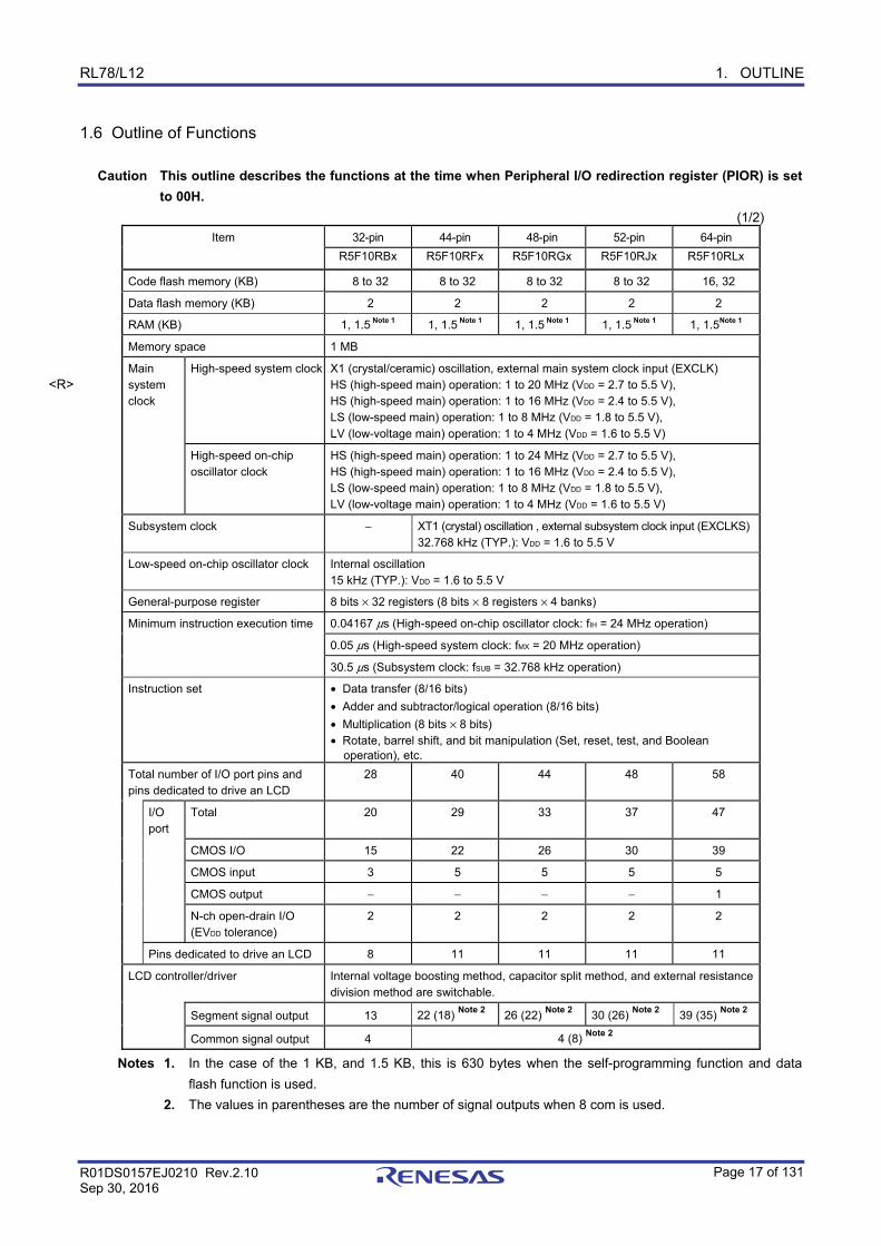
1.6 Outline of Functions
Caution This outline describes the functions at the time when Peripheral I/O redirection register (PIOR) is set to 00H.
(1/2)
Item 32-pin 44-pin 48-pin 52-pin 64-pin
R5F10RBx R5F10RFx R5F10RGx R5F10RJx R5F10RLx
Code flash memory (KB) 8 to 32 8 to 32 8 to 32 8 to 32 16, 32
Data flash memory (KB) 2 2 2 2 2
RAM (KB) 1, 1.5 Note 1 1, 1.5 Note 1 1, 1.5 Note 1 1, 1.5 Note 1 1, 1.5Note 1
Memory space 1 MB
Main system clock
High-speed system clock X1 (crystal/ceramic) oscillation, external main system clock input (EXCLK) HS (high-speed main) operation: 1 to 20 MHz (VDD = 2.7 to 5.5 V), HS (high-speed main) operation: 1 to 16 MHz (VDD = 2.4 to 5.5 V), LS (low-speed main) operation: 1 to 8 MHz (VDD = 1.8 to 5.5 V), LV (low-voltage main) operation: 1 to 4 MHz (VDD = 1.6 to 5.5 V)
High-speed on-chip oscillator clock
HS (high-speed main) operation: 1 to 24 MHz (VDD = 2.7 to 5.5 V), HS (high-speed main) operation: 1 to 16 MHz (VDD = 2.4 to 5.5 V), LS (low-speed main) operation: 1 to 8 MHz (VDD = 1.8 to 5.5 V), LV (low-voltage main) operation: 1 to 4 MHz (VDD = 1.6 to 5.5 V)
Subsystem clock − XT1 (crystal) oscillation , external subsystem clock input (EXCLKS)32.768 kHz (TYP.): VDD = 1.6 to 5.5 V
Low-speed on-chip oscillator clock Internal oscillation 15 kHz (TYP.): VDD = 1.6 to 5.5 V
General-purpose register 8 bits × 32 registers (8 bits × 8 registers × 4 banks)
Minimum instruction execution time 0.04167 μs (High-speed on-chip oscillator clock: fIH = 24 MHz operation)
0.05 μs (High-speed system clock: fMX = 20 MHz operation)
30.5 μs (Subsystem clock: fSUB = 32.768 kHz operation)
Instruction set • Data transfer (8/16 bits)
• Adder and subtractor/logical operation (8/16 bits)
• Multiplication (8 bits × 8 bits) • Rotate, barrel shift, and bit manipulation (Set, reset, test, and Boolean
operation), etc.
Total number of I/O port pins and pins dedicated to drive an LCD
28 40 44 48 58
I/O port
Total 20 29 33 37 47
CMOS I/O 15 22 26 30 39
CMOS input 3 5 5 5 5
CMOS output − − − − 1
N-ch open-drain I/O (EVDD tolerance)
2 2 2 2 2
Pins dedicated to drive an LCD 8 11 11 11 11
LCD controller/driver Internal voltage boosting method, capacitor split method, and external resistance division method are switchable.
Segment signal output 13 22 (18) Note 2
26 (22) Note 2
30 (26) Note 2
39 (35) Note 2
Common signal output 4 4 (8) Note 2
Notes 1. In the case of the 1 KB, and 1.5 KB, this is 630 bytes when the self-programming function and data
flash function is used.
2. The values in parentheses are the number of signal outputs when 8 com is used.
<R>
RL78/L12 1. OUTLINE
R01DS0157EJ0210 Rev.2.10 Sep 30, 2016
Page 18 of 131
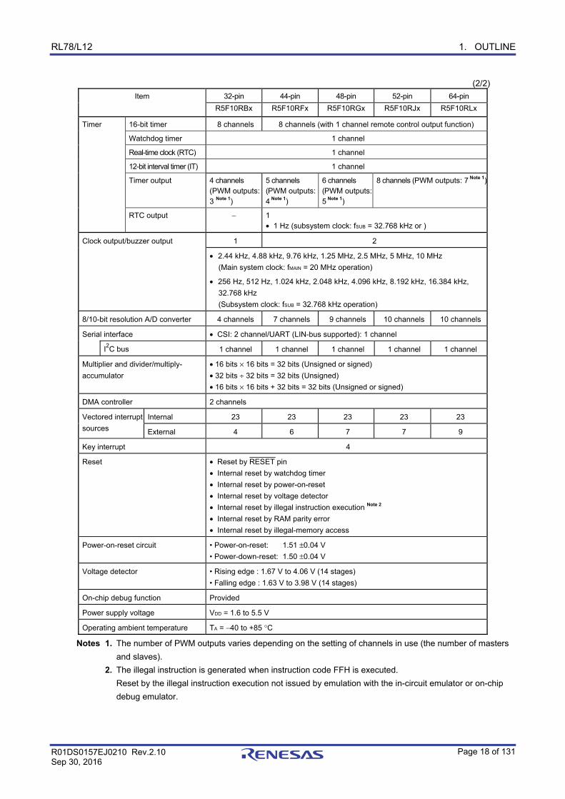
(2/2)
Item 32-pin 44-pin 48-pin 52-pin 64-pin
R5F10RBx R5F10RFx R5F10RGx R5F10RJx R5F10RLx
Timer 16-bit timer 8 channels 8 channels (with 1 channel remote control output function)
Watchdog timer 1 channel
Real-time clock (RTC) 1 channel
12-bit interval timer (IT) 1 channel
Timer output 4 channels (PWM outputs: 3 Note 1)
5 channels (PWM outputs: 4 Note 1)
6 channels (PWM outputs: 5 Note 1)
8 channels (PWM outputs: 7 Note 1)
RTC output − 1 • 1 Hz (subsystem clock: fSUB = 32.768 kHz or )
Clock output/buzzer output 1 2
• 2.44 kHz, 4.88 kHz, 9.76 kHz, 1.25 MHz, 2.5 MHz, 5 MHz, 10 MHz
(Main system clock: fMAIN = 20 MHz operation)
• 256 Hz, 512 Hz, 1.024 kHz, 2.048 kHz, 4.096 kHz, 8.192 kHz, 16.384 kHz,
32.768 kHz
(Subsystem clock: fSUB = 32.768 kHz operation)
8/10-bit resolution A/D converter 4 channels 7 channels 9 channels 10 channels 10 channels
Serial interface • CSI: 2 channel/UART (LIN-bus supported): 1 channel
I2C bus 1 channel 1 channel 1 channel 1 channel 1 channel
Multiplier and divider/multiply-
accumulator
• 16 bits × 16 bits = 32 bits (Unsigned or signed)
• 32 bits ÷ 32 bits = 32 bits (Unsigned)
• 16 bits × 16 bits + 32 bits = 32 bits (Unsigned or signed)
DMA controller 2 channels
Vectored interrupt
sources
Internal 23 23 23 23 23
External 4 6 7 7 9
Key interrupt 4
Reset • Reset by RESET pin
• Internal reset by watchdog timer
• Internal reset by power-on-reset
• Internal reset by voltage detector
• Internal reset by illegal instruction execution Note 2
• Internal reset by RAM parity error
• Internal reset by illegal-memory access
Power-on-reset circuit • Power-on-reset: 1.51 ±0.04 V
• Power-down-reset: 1.50 ±0.04 V
Voltage detector • Rising edge : 1.67 V to 4.06 V (14 stages)
• Falling edge : 1.63 V to 3.98 V (14 stages)
On-chip debug function Provided
Power supply voltage VDD = 1.6 to 5.5 V
Operating ambient temperature TA = −40 to +85 °C
Notes 1. The number of PWM outputs varies depending on the setting of channels in use (the number of masters
and slaves).
2. The illegal instruction is generated when instruction code FFH is executed.
Reset by the illegal instruction execution not issued by emulation with the in-circuit emulator or on-chip
debug emulator.
RL78/L12 2. ELECTRICAL SPECIFICATIONS (A, G: TA = -40 to +85°C)
R01DS0157EJ0210 Rev.2.10 Sep 30, 2016
Page 19 of 131
2. ELECTRICAL SPECIFICATIONS (A, G: TA = -40 to +85°C)
This chapter describes the electrical specifications for the products "A: Consumer applications (TA = -40 to +85°C)" and
"G: Industrial applications (with TA = -40 to +85°C)".
Cautions 1. The RL78 microcontrollers have an on-chip debug function, which is provided for development and evaluation. Do not use the on-chip debug function in products designated for mass production, because the guaranteed number of rewritable times of the flash memory may be exceeded when this function is used, and product reliability therefore cannot be guaranteed. Renesas Electronics is not liable for problems occurring when the on-chip debug function is used.
2. With products not provided with an EVDD, or EVSS pin, replace EVDD with VDD, or replace EVSS with VSS.
RL78/L12 2. ELECTRICAL SPECIFICATIONS (A, G: TA = -40 to +85°C)
R01DS0157EJ0210 Rev.2.10 Sep 30, 2016
Page 20 of 131
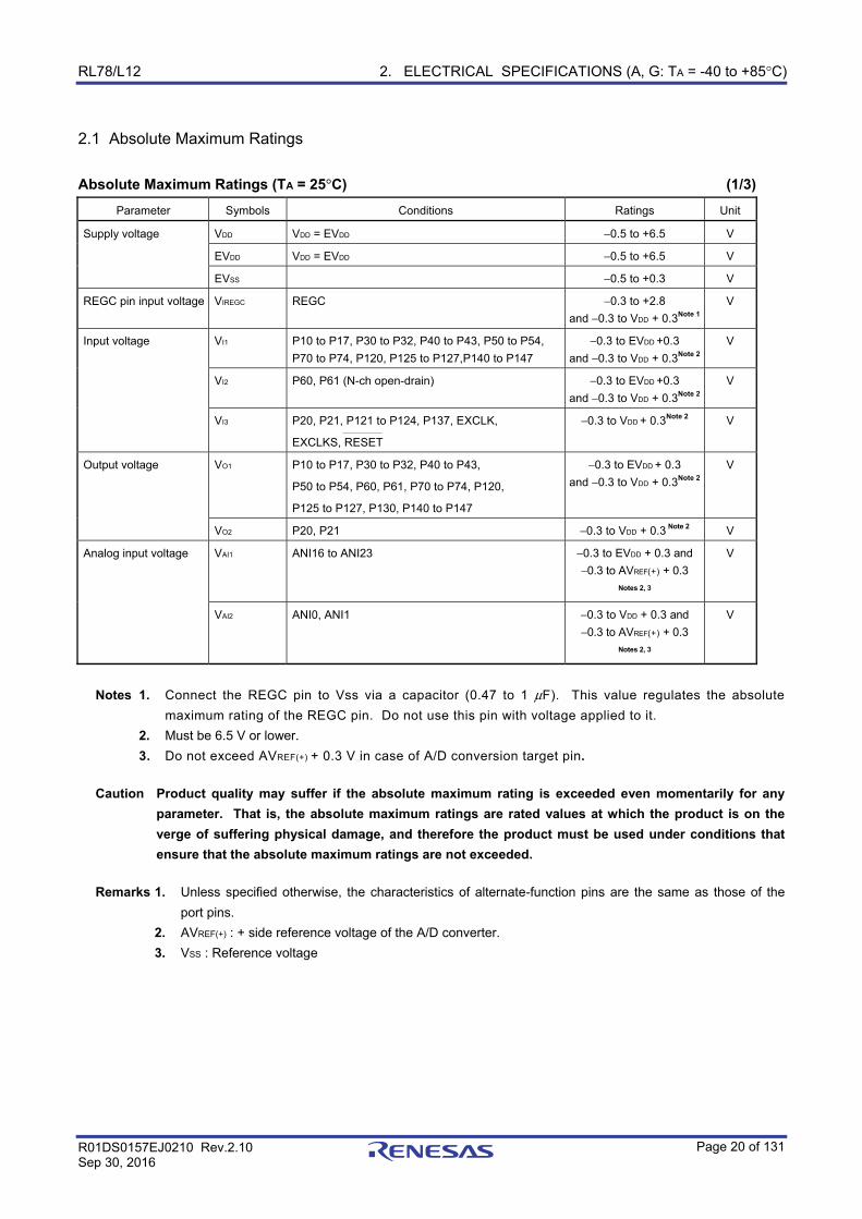
2.1 Absolute Maximum Ratings Absolute Maximum Ratings (TA = 25°C) (1/3)
Parameter Symbols Conditions Ratings Unit
Supply voltage VDD VDD = EVDD −0.5 to +6.5 V
EVDD VDD = EVDD −0.5 to +6.5 V
EVSS −0.5 to +0.3 V
REGC pin input voltage VIREGC REGC −0.3 to +2.8
and −0.3 to VDD + 0.3Note 1
V
Input voltage VI1 P10 to P17, P30 to P32, P40 to P43, P50 to P54,
P70 to P74, P120, P125 to P127,P140 to P147
−0.3 to EVDD +0.3
and −0.3 to VDD + 0.3Note 2
V
VI2 P60, P61 (N-ch open-drain) −0.3 to EVDD +0.3
and −0.3 to VDD + 0.3Note 2
V
VI3 P20, P21, P121 to P124, P137, EXCLK,
EXCLKS, RESET
−0.3 to VDD + 0.3Note 2 V
Output voltage VO1 P10 to P17, P30 to P32, P40 to P43,
P50 to P54, P60, P61, P70 to P74, P120,
P125 to P127, P130, P140 to P147
−0.3 to EVDD + 0.3
and −0.3 to VDD + 0.3Note 2
V
VO2 P20, P21 −0.3 to VDD + 0.3 Note 2 V
Analog input voltage VAI1 ANI16 to ANI23 −0.3 to EVDD + 0.3 and
−0.3 to AVREF(+) + 0.3 Notes 2, 3
V
VAI2 ANI0, ANI1 −0.3 to VDD + 0.3 and
−0.3 to AVREF(+) + 0.3 Notes 2, 3
V
Notes 1. Connect the REGC pin to Vss via a capacitor (0.47 to 1 μF). This value regulates the absolute
maximum rating of the REGC pin. Do not use this pin with voltage applied to it.
2. Must be 6.5 V or lower.
3. Do not exceed AVREF(+) + 0.3 V in case of A/D conversion target pin.
Caution Product quality may suffer if the absolute maximum rating is exceeded even momentarily for any parameter. That is, the absolute maximum ratings are rated values at which the product is on the verge of suffering physical damage, and therefore the product must be used under conditions that ensure that the absolute maximum ratings are not exceeded.
Remarks 1. Unless specified otherwise, the characteristics of alternate-function pins are the same as those of the
port pins.
2. AVREF(+) : + side reference voltage of the A/D converter.
3. VSS : Reference voltage
RL78/L12 2. ELECTRICAL SPECIFICATIONS (A, G: TA = -40 to +85°C)
R01DS0157EJ0210 Rev.2.10 Sep 30, 2016
Page 21 of 131
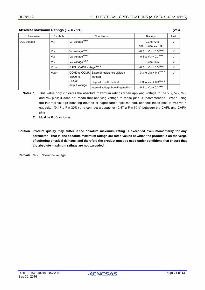
Absolute Maximum Ratings (TA = 25°C) (2/3) Parameter Symbols Conditions Ratings Unit
LCD voltage VL1 VL1 voltageNote 1 −0.3 to +2.8
and −0.3 to VL4 + 0.3
V
VL2 VL2 voltageNote 1 −0.3 to VL4 + 0.3 Note 2 V
VL3 VL3 voltageNote 1 −0.3 to VL4 + 0.3 Note 2 V
VL4 VL4 voltageNote 1 −0.3 to +6.5 V
VLCAP CAPL, CAPH voltageNote 1 −0.3 to VL4 + 0.3 Note 2 V
VLOUT COM0 to COM7,
SEG0 to
SEG38,
output voltage
External resistance division
method
−0.3 to VDD + 0.3 Note 2 V
Capacitor split method −0.3 to VDD + 0.3 Note 2
Internal voltage boosting method −0.3 to VL4 + 0.3 Note 2
Notes 1. This value only indicates the absolute maximum ratings when applying voltage to the VL1, VL2, VL3,
and VL4 pins; it does not mean that applying voltage to these pins is recommended. When using
the internal voltage boosting method or capacitance split method, connect these pins to VSS via a
capacitor (0.47 μ F ± 30%) and connect a capacitor (0.47 μ F ± 30%) between the CAPL and CAPH
pins.
2. Must be 6.5 V or lower.
Caution Product quality may suffer if the absolute maximum rating is exceeded even momentarily for any parameter. That is, the absolute maximum ratings are rated values at which the product is on the verge of suffering physical damage, and therefore the product must be used under conditions that ensure that the absolute maximum ratings are not exceeded.
Remark VSS : Reference voltage
RL78/L12 2. ELECTRICAL SPECIFICATIONS (A, G: TA = -40 to +85°C)
R01DS0157EJ0210 Rev.2.10 Sep 30, 2016
Page 22 of 131
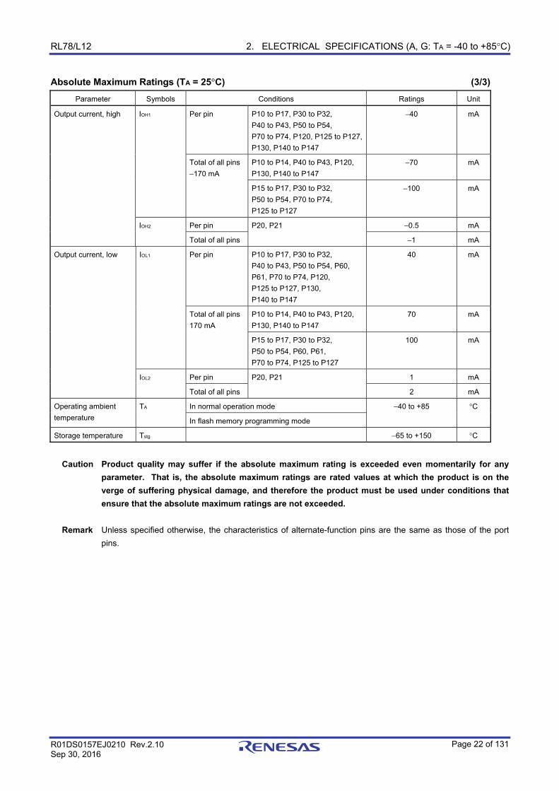
Absolute Maximum Ratings (TA = 25°C) (3/3) Parameter Symbols Conditions Ratings Unit
Output current, high IOH1 Per pin P10 to P17, P30 to P32,
P40 to P43, P50 to P54,
P70 to P74, P120, P125 to P127,
P130, P140 to P147
−40 mA
Total of all pins
−170 mA
P10 to P14, P40 to P43, P120,
P130, P140 to P147
−70 mA
P15 to P17, P30 to P32,
P50 to P54, P70 to P74,
P125 to P127
−100 mA
IOH2 Per pin P20, P21 −0.5 mA
Total of all pins −1 mA
Output current, low IOL1 Per pin P10 to P17, P30 to P32,
P40 to P43, P50 to P54, P60,
P61, P70 to P74, P120,
P125 to P127, P130,
P140 to P147
40 mA
Total of all pins
170 mA
P10 to P14, P40 to P43, P120,
P130, P140 to P147
70 mA
P15 to P17, P30 to P32,
P50 to P54, P60, P61,
P70 to P74, P125 to P127
100 mA
IOL2 Per pin P20, P21 1 mA
Total of all pins 2 mA
Operating ambient
temperature
TA In normal operation mode −40 to +85 °C
In flash memory programming mode
Storage temperature Tstg −65 to +150 °C
Caution Product quality may suffer if the absolute maximum rating is exceeded even momentarily for any
parameter. That is, the absolute maximum ratings are rated values at which the product is on the verge of suffering physical damage, and therefore the product must be used under conditions that ensure that the absolute maximum ratings are not exceeded.
Remark Unless specified otherwise, the characteristics of alternate-function pins are the same as those of the port
pins.
RL78/L12 2. ELECTRICAL SPECIFICATIONS (A, G: TA = -40 to +85°C)
R01DS0157EJ0210 Rev.2.10 Sep 30, 2016
Page 23 of 131
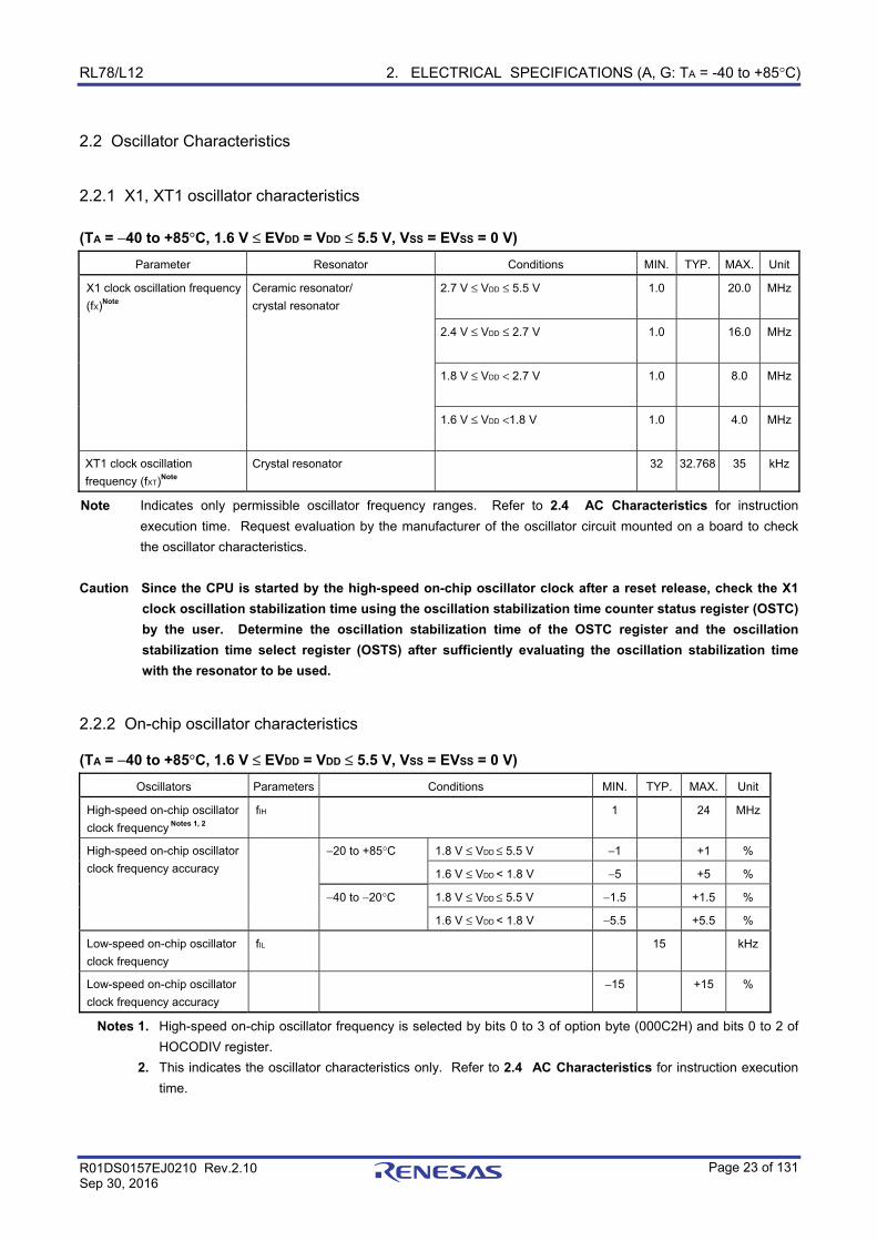
2.2 Oscillator Characteristics
2.2.1 X1, XT1 oscillator characteristics (TA = −40 to +85°C, 1.6 V ≤ EVDD = VDD ≤ 5.5 V, VSS = EVSS = 0 V)
Parameter Resonator Conditions MIN. TYP. MAX. Unit
X1 clock oscillation frequency
(fX)Note
Ceramic resonator/
crystal resonator
2.7 V ≤ VDD ≤ 5.5 V 1.0 20.0 MHz
2.4 V ≤ VDD ≤ 2.7 V 1.0 16.0 MHz
1.8 V ≤ VDD < 2.7 V 1.0 8.0 MHz
1.6 V ≤ VDD <1.8 V 1.0 4.0 MHz
XT1 clock oscillation
frequency (fXT)Note
Crystal resonator 32 32.768 35 kHz
Note Indicates only permissible oscillator frequency ranges. Refer to 2.4 AC Characteristics for instruction
execution time. Request evaluation by the manufacturer of the oscillator circuit mounted on a board to check
the oscillator characteristics.
Caution Since the CPU is started by the high-speed on-chip oscillator clock after a reset release, check the X1 clock oscillation stabilization time using the oscillation stabilization time counter status register (OSTC) by the user. Determine the oscillation stabilization time of the OSTC register and the oscillation stabilization time select register (OSTS) after sufficiently evaluating the oscillation stabilization time with the resonator to be used.
2.2.2 On-chip oscillator characteristics (TA = −40 to +85°C, 1.6 V ≤ EVDD = VDD ≤ 5.5 V, VSS = EVSS = 0 V)
Oscillators Parameters Conditions MIN. TYP. MAX. Unit
High-speed on-chip oscillator
clock frequency Notes 1, 2
fIH 1 24 MHz
High-speed on-chip oscillator
clock frequency accuracy
−20 to +85°C 1.8 V ≤ VDD ≤ 5.5 V −1 +1 %
1.6 V ≤ VDD < 1.8 V −5 +5 %
−40 to −20°C 1.8 V ≤ VDD ≤ 5.5 V −1.5 +1.5 %
1.6 V ≤ VDD < 1.8 V −5.5 +5.5 %
Low-speed on-chip oscillator
clock frequency
fIL 15 kHz
Low-speed on-chip oscillator
clock frequency accuracy
−15 +15 %
Notes 1. High-speed on-chip oscillator frequency is selected by bits 0 to 3 of option byte (000C2H) and bits 0 to 2 of
HOCODIV register.
2. This indicates the oscillator characteristics only. Refer to 2.4 AC Characteristics for instruction execution
time.
RL78/L12 2. ELECTRICAL SPECIFICATIONS (A, G: TA = -40 to +85°C)
R01DS0157EJ0210 Rev.2.10 Sep 30, 2016
Page 24 of 131
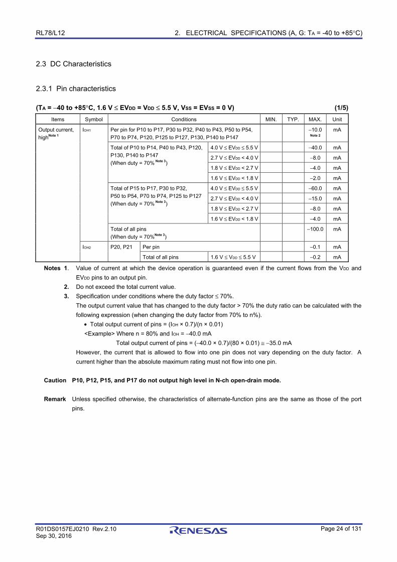
2.3 DC Characteristics
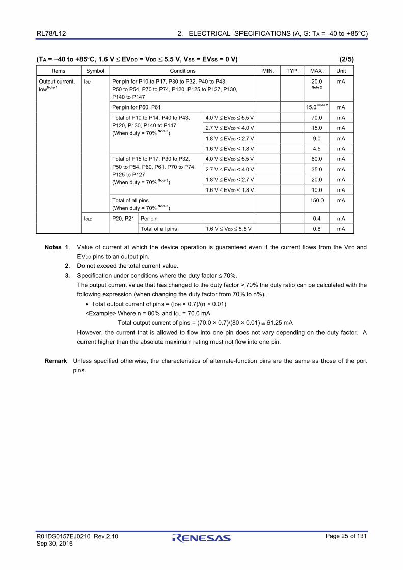
2.3.1 Pin characteristics (TA = −40 to +85°C, 1.6 V ≤ EVDD = VDD ≤ 5.5 V, VSS = EVSS = 0 V) (1/5)
Items Symbol Conditions MIN. TYP. MAX. Unit
Output current,
highNote 1
IOH1 Per pin for P10 to P17, P30 to P32, P40 to P43, P50 to P54,
P70 to P74, P120, P125 to P127, P130, P140 to P147
−10.0 Note 2
mA
Total of P10 to P14, P40 to P43, P120,
P130, P140 to P147
(When duty = 70% Note 3)
4.0 V ≤ EVDD ≤ 5.5 V −40.0 mA
2.7 V ≤ EVDD < 4.0 V −8.0 mA
1.8 V ≤ EVDD < 2.7 V −4.0 mA
1.6 V ≤ EVDD < 1.8 V −2.0 mA
Total of P15 to P17, P30 to P32,
P50 to P54, P70 to P74, P125 to P127
(When duty = 70% Note 3)
4.0 V ≤ EVDD ≤ 5.5 V −60.0 mA
2.7 V ≤ EVDD < 4.0 V −15.0 mA
1.8 V ≤ EVDD < 2.7 V −8.0 mA
1.6 V ≤ EVDD < 1.8 V −4.0 mA
Total of all pins
(When duty = 70%Note 3)
−100.0 mA
IOH2 P20, P21 Per pin −0.1 mA
Total of all pins 1.6 V ≤ VDD ≤ 5.5 V −0.2 mA
Notes 1. Value of current at which the device operation is guaranteed even if the current flows from the VDD and
EVDD pins to an output pin.
2. Do not exceed the total current value.
3. Specification under conditions where the duty factor ≤ 70%.
The output current value that has changed to the duty factor > 70% the duty ratio can be calculated with the
following expression (when changing the duty factor from 70% to n%).
• Total output current of pins = (IOH × 0.7)/(n × 0.01)
<Example> Where n = 80% and IOH = −40.0 mA
Total output current of pins = (−40.0 × 0.7)/(80 × 0.01) ≅ −35.0 mA
However, the current that is allowed to flow into one pin does not vary depending on the duty factor. A
current higher than the absolute maximum rating must not flow into one pin.
Caution P10, P12, P15, and P17 do not output high level in N-ch open-drain mode.
Remark Unless specified otherwise, the characteristics of alternate-function pins are the same as those of the port
pins.
RL78/L12 2. ELECTRICAL SPECIFICATIONS (A, G: TA = -40 to +85°C)
R01DS0157EJ0210 Rev.2.10 Sep 30, 2016
Page 25 of 131
(TA = −40 to +85°C, 1.6 V ≤ EVDD = VDD ≤ 5.5 V, VSS = EVSS = 0 V) (2/5) Items Symbol Conditions MIN. TYP. MAX. Unit
Output current,
lowNote 1
IOL1 Per pin for P10 to P17, P30 to P32, P40 to P43,
P50 to P54, P70 to P74, P120, P125 to P127, P130,
P140 to P147
20.0 Note 2
mA
Per pin for P60, P61 15.0 Note 2 mA
Total of P10 to P14, P40 to P43,
P120, P130, P140 to P147
(When duty = 70% Note 3)
4.0 V ≤ EVDD ≤ 5.5 V 70.0 mA
2.7 V ≤ EVDD < 4.0 V 15.0 mA
1.8 V ≤ EVDD < 2.7 V 9.0 mA
1.6 V ≤ EVDD < 1.8 V 4.5 mA
Total of P15 to P17, P30 to P32,
P50 to P54, P60, P61, P70 to P74,
P125 to P127
(When duty = 70% Note 3)
4.0 V ≤ EVDD ≤ 5.5 V 80.0 mA
2.7 V ≤ EVDD < 4.0 V 35.0 mA
1.8 V ≤ EVDD < 2.7 V 20.0 mA
1.6 V ≤ EVDD < 1.8 V 10.0 mA
Total of all pins
(When duty = 70% Note 3)
150.0 mA
IOL2 P20, P21 Per pin 0.4 mA
Total of all pins 1.6 V ≤ VDD ≤ 5.5 V 0.8 mA
Notes 1. Value of current at which the device operation is guaranteed even if the current flows from the VDD and
EVDD pins to an output pin.
2. Do not exceed the total current value.
3. Specification under conditions where the duty factor ≤ 70%.
The output current value that has changed to the duty factor > 70% the duty ratio can be calculated with the
following expression (when changing the duty factor from 70% to n%).
• Total output current of pins = (IOH × 0.7)/(n × 0.01)
<Example> Where n = 80% and IOL = 70.0 mA
Total output current of pins = (70.0 × 0.7)/(80 × 0.01) ≅ 61.25 mA
However, the current that is allowed to flow into one pin does not vary depending on the duty factor. A
current higher than the absolute maximum rating must not flow into one pin.
Remark Unless specified otherwise, the characteristics of alternate-function pins are the same as those of the port
pins.
RL78/L12 2. ELECTRICAL SPECIFICATIONS (A, G: TA = -40 to +85°C)
R01DS0157EJ0210 Rev.2.10 Sep 30, 2016
Page 26 of 131
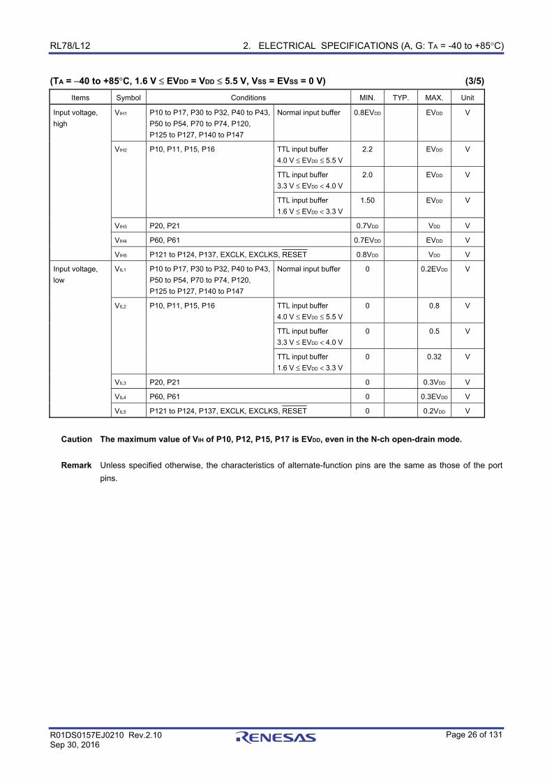
(TA = −40 to +85°C, 1.6 V ≤ EVDD = VDD ≤ 5.5 V, VSS = EVSS = 0 V) (3/5) Items Symbol Conditions MIN. TYP. MAX. Unit
Input voltage,
high
VIH1 P10 to P17, P30 to P32, P40 to P43,
P50 to P54, P70 to P74, P120,
P125 to P127, P140 to P147
Normal input buffer
0.8EVDD EVDD V
VIH2 P10, P11, P15, P16 TTL input buffer
4.0 V ≤ EVDD ≤ 5.5 V
2.2 EVDD V
TTL input buffer
3.3 V ≤ EVDD < 4.0 V
2.0 EVDD V
TTL input buffer
1.6 V ≤ EVDD < 3.3 V
1.50 EVDD V
VIH3 P20, P21 0.7VDD VDD V
VIH4 P60, P61 0.7EVDD EVDD V
VIH5 P121 to P124, P137, EXCLK, EXCLKS, RESET 0.8VDD VDD V
Input voltage,
low
VIL1 P10 to P17, P30 to P32, P40 to P43,
P50 to P54, P70 to P74, P120,
P125 to P127, P140 to P147
Normal input buffer
0 0.2EVDD V
VIL2 P10, P11, P15, P16 TTL input buffer
4.0 V ≤ EVDD ≤ 5.5 V
0 0.8 V
TTL input buffer
3.3 V ≤ EVDD < 4.0 V
0 0.5 V
TTL input buffer
1.6 V ≤ EVDD < 3.3 V
0 0.32 V
VIL3 P20, P21 0 0.3VDD V
VIL4 P60, P61 0 0.3EVDD V
VIL5 P121 to P124, P137, EXCLK, EXCLKS, RESET 0 0.2VDD V
Caution The maximum value of VIH of P10, P12, P15, P17 is EVDD, even in the N-ch open-drain mode.
Remark Unless specified otherwise, the characteristics of alternate-function pins are the same as those of the port
pins.
RL78/L12 2. ELECTRICAL SPECIFICATIONS (A, G: TA = -40 to +85°C)
R01DS0157EJ0210 Rev.2.10 Sep 30, 2016
Page 27 of 131
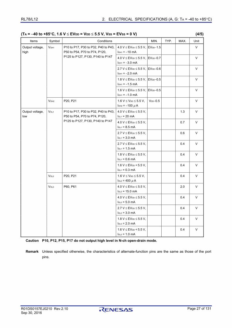
(TA = −40 to +85°C, 1.6 V ≤ EVDD = VDD ≤ 5.5 V, VSS = EVSS = 0 V) (4/5) Items Symbol Conditions MIN. TYP. MAX. Unit
Output voltage,
high
VOH1 P10 to P17, P30 to P32, P40 to P43,
P50 to P54, P70 to P74, P120,
P125 to P127, P130, P140 to P147
4.0 V ≤ EVDD ≤ 5.5 V,
IOH1 = −10 mA
EVDD−1.5 V
4.0 V ≤ EVDD ≤ 5.5 V,
IOH1 = −3.0 mA
EVDD−0.7 V
2.7 V ≤ EVDD ≤ 5.5 V,
IOH1 = −2.0 mA
EVDD−0.6 V
1.8 V ≤ EVDD ≤ 5.5 V,
IOH1 = −1.5 mA
EVDD−0.5 V
1.6 V ≤ EVDD ≤ 5.5 V,
IOH1 = −1.0 mA
EVDD−0.5 V
VOH2 P20, P21 1.6 V ≤ VDD ≤ 5.5 V,
IOH2 = −100 μ A
VDD−0.5 V
Output voltage,
low
VOL1 P10 to P17, P30 to P32, P40 to P43,
P50 to P54, P70 to P74, P120,
P125 to P127, P130, P140 to P147
4.0 V ≤ EVDD ≤ 5.5 V,
IOL1 = 20 mA
1.3 V
4.0 V ≤ EVDD ≤ 5.5 V,
IOL1 = 8.5 mA
0.7 V
2.7 V ≤ EVDD ≤ 5.5 V,
IOL1 = 3.0 mA
0.6 V
2.7 V ≤ EVDD ≤ 5.5 V,
IOL1 = 1.5 mA
0.4 V
1.8 V ≤ EVDD ≤ 5.5 V,
IOL1 = 0.6 mA
0.4 V
1.6 V ≤ EVDD < 5.5 V,
IOL1 = 0.3 mA
0.4 V
VOL2 P20, P21 1.6 V ≤ VDD ≤ 5.5 V,
IOL2 = 400 μ A
0.4 V
VOL3 P60, P61 4.0 V ≤ EVDD ≤ 5.5 V,
IOL3 = 15.0 mA
2.0 V
4.0 V ≤ EVDD ≤ 5.5 V,
IOL3 = 5.0 mA
0.4 V
2.7 V ≤ EVDD ≤ 5.5 V,
IOL3 = 3.0 mA
0.4 V
1.8 V ≤ EVDD ≤ 5.5 V,
IOL3 = 2.0 mA
0.4 V
1.6 V ≤ EVDD < 5.5 V,
IOL3 = 1.0 mA
0.4 V
Caution P10, P12, P15, P17 do not output high level in N-ch open-drain mode.
Remark Unless specified otherwise, the characteristics of alternate-function pins are the same as those of the port
pins.
RL78/L12 2. ELECTRICAL SPECIFICATIONS (A, G: TA = -40 to +85°C)
R01DS0157EJ0210 Rev.2.10 Sep 30, 2016
Page 28 of 131
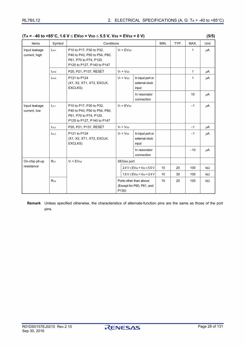
(TA = −40 to +85°C, 1.6 V ≤ EVDD = VDD ≤ 5.5 V, VSS = EVSS = 0 V) (5/5) Items Symbol Conditions MIN. TYP. MAX. Unit
Input leakage
current, high
ILIH1 P10 to P17, P30 to P32,
P40 to P43, P50 to P54, P60,
P61, P70 to P74, P120,
P125 to P127, P140 to P147
VI = EVDD 1 μA
ILIH2 P20, P21, P137, RESET VI = VDD 1 μA
ILIH3 P121 to P124
(X1, X2, XT1, XT2, EXCLK,
EXCLKS)
VI = VDD In input port or
external clock
input
1 μA
In resonator
connection
10 μA
Input leakage
current, low
ILIL1 P10 to P17, P30 to P32,
P40 to P43, P50 to P54, P60,
P61, P70 to P74, P120,
P125 to P127, P140 to P147
VI = EVSS −1 μA
ILIL2 P20, P21, P137, RESET VI = VSS −1 μA
ILIL3 P121 to P124
(X1, X2, XT1, XT2, EXCLK,
EXCLKS)
VI = VSS In input port or
external clock
input
−1 μA
In resonator
connection
−10 μA
On-chip pll-up
resistance
RU1 VI = EVSS SEGxx port
2.4 V ≤ EVDD = VDD ≤ 5.5 V 10 20 100 kΩ
1.6 V ≤ EVDD = VDD < 2.4 V 10 30 100 kΩ
RU2 Ports other than above
(Except for P60, P61, and
P130)
10 20 100 kΩ
Remark Unless specified otherwise, the characteristics of alternate-function pins are the same as those of the port
pins.
RL78/L12 2. ELECTRICAL SPECIFICATIONS (A, G: TA = -40 to +85°C)
R01DS0157EJ0210 Rev.2.10 Sep 30, 2016
Page 29 of 131
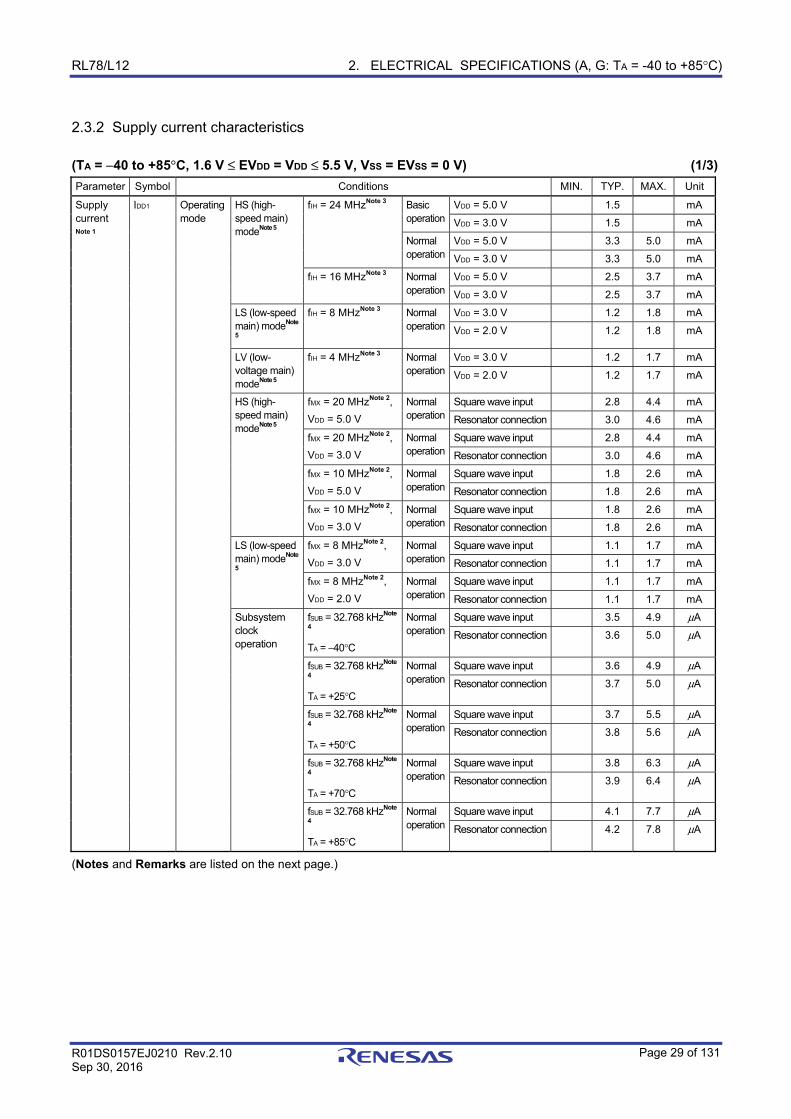
2.3.2 Supply current characteristics (TA = −40 to +85°C, 1.6 V ≤ EVDD = VDD ≤ 5.5 V, VSS = EVSS = 0 V) (1/3) Parameter Symbol Conditions MIN. TYP. MAX. Unit
Supply current Note 1
IDD1 Operating mode
HS (high-speed main) modeNote 5
fIH = 24 MHzNote 3 Basic operation
VDD = 5.0 V 1.5 mA VDD = 3.0 V 1.5 mA
Normal operation
VDD = 5.0 V 3.3 5.0 mA VDD = 3.0 V 3.3 5.0 mA
fIH = 16 MHzNote 3 Normal operation
VDD = 5.0 V 2.5 3.7 mA VDD = 3.0 V 2.5 3.7 mA
LS (low-speed main) modeNote
5
fIH = 8 MHzNote 3 Normal operation
VDD = 3.0 V 1.2 1.8 mA VDD = 2.0 V 1.2 1.8 mA
LV (low-voltage main) modeNote 5
fIH = 4 MHzNote 3 Normal operation
VDD = 3.0 V 1.2 1.7 mA VDD = 2.0 V 1.2 1.7 mA
HS (high-speed main) modeNote 5
fMX = 20 MHzNote 2,
VDD = 5.0 V
Normal operation
Square wave input 2.8 4.4 mA
Resonator connection 3.0 4.6 mA
fMX = 20 MHzNote 2,
VDD = 3.0 V
Normal operation
Square wave input 2.8 4.4 mA Resonator connection 3.0 4.6 mA
fMX = 10 MHzNote 2,
VDD = 5.0 V
Normal operation
Square wave input 1.8 2.6 mA Resonator connection 1.8 2.6 mA
fMX = 10 MHzNote 2,
VDD = 3.0 V
Normal operation
Square wave input 1.8 2.6 mA Resonator connection 1.8 2.6 mA
LS (low-speed main) modeNote
5
fMX = 8 MHzNote 2,
VDD = 3.0 V
Normal operation
Square wave input 1.1 1.7 mA Resonator connection 1.1 1.7 mA
fMX = 8 MHzNote 2,
VDD = 2.0 V
Normal operation
Square wave input 1.1 1.7 mA Resonator connection 1.1 1.7 mA
Subsystem clock operation
fSUB = 32.768 kHzNote
4
TA = −40°C
Normal operation
Square wave input 3.5 4.9 μA
Resonator connection 3.6 5.0 μA
fSUB = 32.768 kHzNote
4
TA = +25°C
Normal operation
Square wave input 3.6 4.9 μA
Resonator connection 3.7 5.0 μA
fSUB = 32.768 kHzNote
4
TA = +50°C
Normal operation
Square wave input 3.7 5.5 μA
Resonator connection 3.8 5.6 μA
fSUB = 32.768 kHzNote
4
TA = +70°C
Normal operation
Square wave input 3.8 6.3 μA
Resonator connection 3.9 6.4 μA
fSUB = 32.768 kHzNote
4
TA = +85°C
Normal operation
Square wave input 4.1 7.7 μA
Resonator connection 4.2 7.8 μA
(Notes and Remarks are listed on the next page.)
RL78/L12 2. ELECTRICAL SPECIFICATIONS (A, G: TA = -40 to +85°C)
R01DS0157EJ0210 Rev.2.10 Sep 30, 2016
Page 30 of 131
Notes 1. Total current flowing into VDD and EVDD, including the input leakage current flowing when the level of the input
pin is fixed to VDD, EVDD or VSS, EVSS. The values below the MAX. column include the peripheral operation
current. However, not including the current flowing into the A/D converter, LVD circuit, I/O port, and on-chip
pull-up/pull-down resistors and the current flowing during data flash rewrite.
2. When high-speed on-chip oscillator and subsystem clock are stopped.
3. When high-speed system clock and subsystem clock are stopped.
4. When high-speed on-chip oscillator and high-speed system clock are stopped. When AMPHS1 = 1 (Ultra-low
power consumption oscillation). However, not including the current flowing into the RTC, 12-bit interval timer,
watchdog timer, and LCD controller/driver.
5. Relationship between operation voltage width, operation frequency of CPU and operation mode is as below.
HS (high-speed main) mode: 2.7 V ≤ VDD ≤ 5.5 V@1 MHz to 24 MHz
2.4 V ≤ VDD ≤ 5.5 V@1 MHz to 16 MHz
LS (low-speed main) mode: 1.8 V ≤ VDD ≤ 5.5 V@1 MHz to 8 MHz
LV (low-voltage main) mode: 1.6 V ≤ VDD ≤ 5.5 V@1 MHz to 4 MHz
Remarks 1. fMX: High-speed system clock frequency (X1 clock oscillation frequency or external main system clock
frequency)
2. fIH: High-speed on-chip oscillator clock frequency
3. fSUB: Subsystem clock frequency (XT1 clock oscillation frequency)
4. Except subsystem clock operation, temperature condition of the TYP. value is TA = 25°C
RL78/L12 2. ELECTRICAL SPECIFICATIONS (A, G: TA = -40 to +85°C)
R01DS0157EJ0210 Rev.2.10 Sep 30, 2016
Page 31 of 131
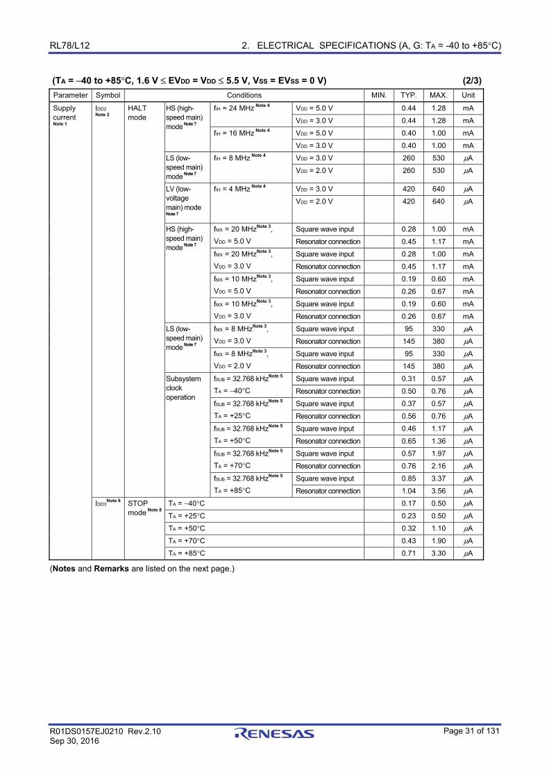
(TA = −40 to +85°C, 1.6 V ≤ EVDD = VDD ≤ 5.5 V, VSS = EVSS = 0 V) (2/3) Parameter Symbol Conditions MIN. TYP. MAX. Unit
Supply current Note 1
IDD2 Note 2
HALT mode
HS (high-speed main) mode Note 7
fIH = 24 MHz Note 4 VDD = 5.0 V 0.44 1.28 mA
VDD = 3.0 V 0.44 1.28 mA
fIH = 16 MHz Note 4 VDD = 5.0 V 0.40 1.00 mA
VDD = 3.0 V 0.40 1.00 mA
LS (low-speed main) mode Note 7
fIH = 8 MHz Note 4 VDD = 3.0 V 260 530 μA
VDD = 2.0 V 260 530 μA
LV (low-voltage main) mode
Note 7
fIH = 4 MHz Note 4 VDD = 3.0 V 420 640 μA
VDD = 2.0 V 420 640 μA
HS (high-speed main) mode Note 7
fMX = 20 MHzNote 3,
VDD = 5.0 V
Square wave input 0.28 1.00 mA
Resonator connection 0.45 1.17 mA
fMX = 20 MHzNote 3,
VDD = 3.0 V
Square wave input 0.28 1.00 mA
Resonator connection 0.45 1.17 mA
fMX = 10 MHzNote 3,
VDD = 5.0 V
Square wave input 0.19 0.60 mA
Resonator connection 0.26 0.67 mA
fMX = 10 MHzNote 3,
VDD = 3.0 V
Square wave input 0.19 0.60 mA
Resonator connection 0.26 0.67 mA
LS (low-speed main) mode Note 7
fMX = 8 MHzNote 3,
VDD = 3.0 V
Square wave input 95 330 μA
Resonator connection 145 380 μA
fMX = 8 MHzNote 3,
VDD = 2.0 V
Square wave input 95 330 μA
Resonator connection 145 380 μA
Subsystem clock operation
fSUB = 32.768 kHzNote 5
TA = −40°C
Square wave input 0.31 0.57 μA
Resonator connection 0.50 0.76 μA
fSUB = 32.768 kHzNote 5
TA = +25°C
Square wave input 0.37 0.57 μA
Resonator connection 0.56 0.76 μA
fSUB = 32.768 kHzNote 5
TA = +50°C
Square wave input 0.46 1.17 μA
Resonator connection 0.65 1.36 μA
fSUB = 32.768 kHzNote 5
TA = +70°C
Square wave input 0.57 1.97 μA
Resonator connection 0.76 2.16 μA
fSUB = 32.768 kHzNote 5
TA = +85°C
Square wave input 0.85 3.37 μA
Resonator connection 1.04 3.56 μA
IDD3Note 6 STOP
mode Note 8TA = −40°C 0.17 0.50 μA
TA = +25°C 0.23 0.50 μA
TA = +50°C 0.32 1.10 μA
TA = +70°C 0.43 1.90 μA
TA = +85°C 0.71 3.30 μA
(Notes and Remarks are listed on the next page.)
RL78/L12 2. ELECTRICAL SPECIFICATIONS (A, G: TA = -40 to +85°C)
R01DS0157EJ0210 Rev.2.10 Sep 30, 2016
Page 32 of 131
Notes 1. Total current flowing into VDD and EVDD, including the input leakage current flowing when the level of the input
pin is fixed to VDD, EVDD or VSS, EVSS. The values below the MAX. column include the peripheral operation
current. However, not including the current flowing into the A/D converter, LVD circuit, I/O port, and on-chip
pull-up/pull-down resistors and the current flowing during data flash rewrite.
2. During HALT instruction execution by flash memory.
3. When high-speed on-chip oscillator and subsystem clock are stopped.
4. When high-speed system clock and subsystem clock are stopped.
5. When high-speed on-chip oscillator and high-speed system clock are stopped. When RTCLPC = 1 and setting
ultra-low current consumption (AMPHS1 = 1). The current flowing into the RTC is included. However, not
including the current flowing into the 12-bit interval timer, watchdog timer, and LCD controller/driver.
6. Not including the current flowing into the RTC, 12-bit interval timer, and watchdog timer.
7. Relationship between operation voltage width, operation frequency of CPU and operation mode is as below.
HS (high-speed main) mode: 2.7 V ≤ VDD ≤ 5.5 V@1 MHz to 24 MHz
2.4 V ≤ VDD ≤ 5.5 V@1 MHz to 16 MHz
LS (low-speed main) mode: 1.8 V ≤ VDD ≤ 5.5 V@1 MHz to 8 MHz
LV (low-voltage main) mode: 1.6 V ≤ VDD ≤ 5.5 V@1 MHz to 4 MHz
8. Regarding the value for current to operate the subsystem clock in STOP mode, refer to that in HALT mode.
Remarks 1. fMX: High-speed system clock frequency (X1 clock oscillation frequency or external main system clock
frequency)
2. fIH: High-speed on-chip oscillator clock frequency
3. fSUB: Subsystem clock frequency (XT1 clock oscillation frequency)
4. Except subsystem clock operation and STOP mode, temperature condition of the TYP. value is TA = 25°C

RL78/L12 2. ELECTRICAL SPECIFICATIONS (A, G: TA = -40 to +85°C)
R01DS0157EJ0210 Rev.2.10 Sep 30, 2016
Page 33 of 131
(TA = −40 to +85°C, 1.6 V ≤ EVDD = VDD ≤ 5.5 V, VSS = EVSS = 0 V) (3/3) Parameter Symbol Conditions MIN. TYP. MAX. Unit
Low-speed on-
chip oscillator
operating
current
IFIL Note 1 0.20 μA
RTC operating
current
IRTC
Notes 1, 2, 3
fMAIN is stopped 0.08 μA
12-bit interval
timer current
IIT
Notes 1, 2, 4
0.08 μA
Watchdog timer
operating
current
IWDT
Notes 1, 2, 5
fIL = 15 kHz 0.24 μA
A/D converter operating current
IADC
Notes 1, 6
When conversion at maximum speed
Normal mode, AVREFP = VDD = 5.0 V 1.3 1.7 mA
Low voltage mode, AVREFP = VDD = 3.0 V 0.5 0.7 mA
A/D converter reference voltage current
IADREF Note 1 75.0 μA
Temperature sensor operating current
ITMPS Note 1 75.0 μA
LVD operating
current
ILVD
Notes 1, 7
0.08 μA
Self-
programming
operating
current
IFSP
Notes 1, 9
2.50 12.20 mA
BGO operating
current
IBGO
Notes 1, 8
2.00 12.20 mA
LCD operating
current
ILCD1
Notes 11, 12
External resistance division method VDD = EVDD = 5.0 V
VL4 = 5.0 V
0.04 0.20 μA
ILCD2 Note 11 Internal voltage boosting method VDD = EVDD = 5.0 V
VL4 = 5.1 V (VLCD = 12H)
1.12 3.70 μA
VDD = EVDD = 3.0 V
VL4 = 3.0 V (VLCD = 04H)
0.63 2.20 μA
ILCD3 Note 11 Capacitor split method VDD = EVDD = 3.0 V
VL4 = 3.0 V
0.12 0.50 μA
SNOOZE
operating
current
ISNOZ Note 1 ADC operation The mode is performed Note 10 0.50 0.60 mA
The A/D conversion operations are
performed, Low voltage mode, AVREFP = VDD
= 3.0 V
1.20 1.44 mA
CSI/UART operation 0.70 0.84 mA
(Notes and Remarks are listed on the next page.)
RL78/L12 2. ELECTRICAL SPECIFICATIONS (A, G: TA = -40 to +85°C)
R01DS0157EJ0210 Rev.2.10 Sep 30, 2016
Page 34 of 131
Notes 1. Current flowing to VDD.
2. When high speed on-chip oscillator and high-speed system clock are stopped.
3. Current flowing only to the real-time clock (RTC) (excluding the operating current of the low-speed on-chip
oscillator and the XT1 oscillator). The supply current of the RL78 microcontrollers is the sum of the values of
either IDD1 or IDD2, and IRTC, when the real-time clock operates in operation mode or HALT mode. When the
low-speed on-chip oscillator is selected, IFIL should be added. IDD2 subsystem clock operation includes the
operational current of the real-time clock.
4. Current flowing only to the 12-bit interval timer (excluding the operating current of the low-speed on-chip
oscillator and the XT1 oscillator). The supply current of the RL78 microcontrollers is the sum of the values of
either IDD1 or IDD2, and IIT, when the 12-bit interval timer operates in operation mode or HALT mode. When the
low-speed on-chip oscillator is selected, IFIL should be added.
5. Current flowing only to the watchdog timer (including the operating current of the low-speed on-chip oscillator).
The supply current of the RL78 microcontrollers is the sum of IDD1, IDD2 or IDD3 and IWDT when the watchdog
timer is in operation.
6. Current flowing only to the A/D converter. The supply current of the RL78 microcontrollers is the sum of IDD1 or
IDD2 and IADC when the A/D converter operates in an operation mode or the HALT mode.
7. Current flowing only to the LVD circuit. The supply current of the RL78 microcontrollers is the sum of IDD1, IDD2
or IDD3 and ILVD when the LVD circuit is in operation.
8. Current flowing only during data flash rewrite.
9. Current flowing only during self programming.
10. For shift time to the SNOOZE mod. 11. Current flowing only to the LCD controller/driver. The supply current value of the RL78 microcontrollers is the
sum of the LCD operating current (ILCD1, ILCD2 or ILCD3) to the supply current (IDD1 or IDD2) when the LCD
controller/driver operates in an operation mode or HALT mode. Not including the current that flows through the
LCD panel.
The TYP. value and MAX. value are following conditions.
• When fSUB is selected for system clock, LCD clock = 128 Hz (LCDC0 = 07H)
• 4-Time-Slice, 1/3 Bias Method
12. Not including the current that flows through the external divider resistor when the external resistance division
method is used.
Remarks 1. fIL: Low-speed on-chip oscillator clock frequency
2. fSUB: Subsystem clock frequency (XT1 clock oscillation frequency)
3. fCLK: CPU/peripheral hardware clock frequency
4. Temperature condition of the TYP. value is TA = 25°C
RL78/L12 2. ELECTRICAL SPECIFICATIONS (A, G: TA = -40 to +85°C)
R01DS0157EJ0210 Rev.2.10 Sep 30, 2016
Page 35 of 131
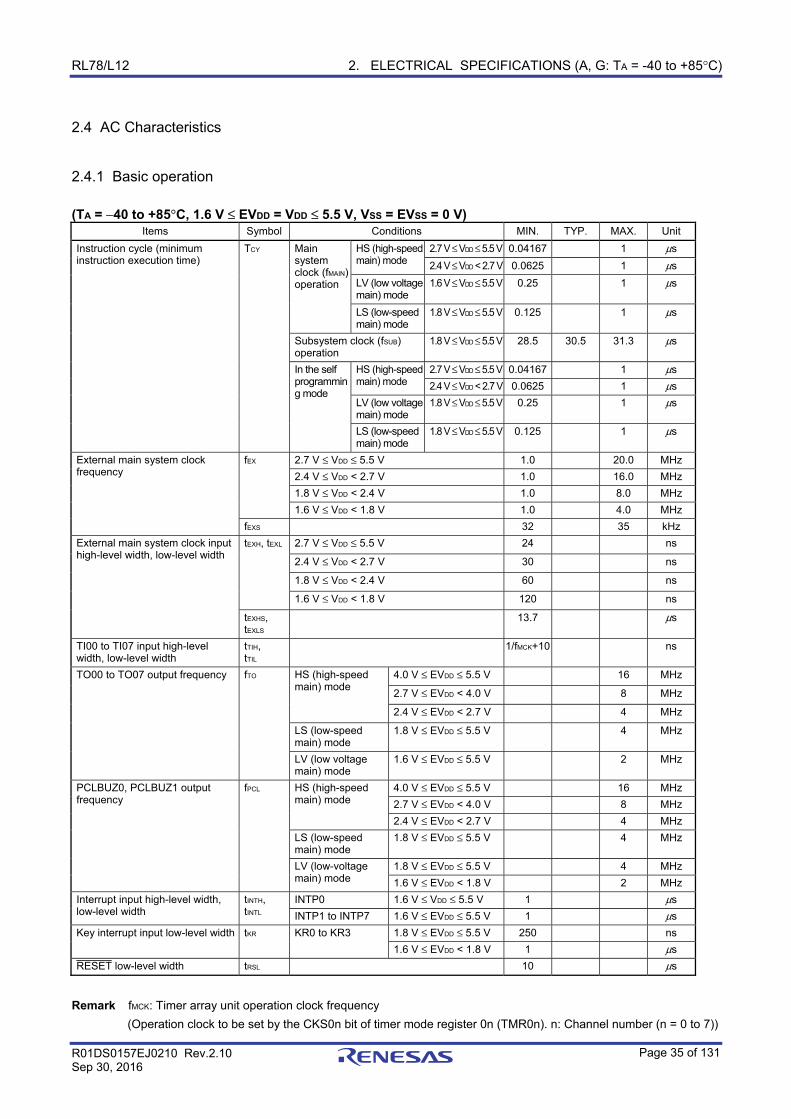
2.4 AC Characteristics
2.4.1 Basic operation (TA = −40 to +85°C, 1.6 V ≤ EVDD = VDD ≤ 5.5 V, VSS = EVSS = 0 V)
Items Symbol Conditions MIN. TYP. MAX. Unit
Instruction cycle (minimum instruction execution time)
TCY Main system clock (fMAIN) operation
HS (high-speed main) mode
2.7 V ≤ VDD ≤ 5.5 V 0.04167 1 μs 2.4 V ≤ VDD < 2.7 V 0.0625 1 μs
LV (low voltage main) mode
1.6 V ≤ VDD ≤ 5.5 V 0.25 1 μs
LS (low-speed main) mode
1.8 V ≤ VDD ≤ 5.5 V 0.125 1 μs
Subsystem clock (fSUB) operation
1.8 V ≤ VDD ≤ 5.5 V 28.5 30.5 31.3 μs
In the self programming mode
HS (high-speed main) mode
2.7 V ≤ VDD ≤ 5.5 V 0.04167 1 μs
2.4 V ≤ VDD < 2.7 V 0.0625 1 μs
LV (low voltage main) mode
1.8 V ≤ VDD ≤ 5.5 V 0.25 1 μs
LS (low-speed main) mode
1.8 V ≤ VDD ≤ 5.5 V 0.125 1 μs
External main system clock frequency
fEX 2.7 V ≤ VDD ≤ 5.5 V 1.0 20.0 MHz 2.4 V ≤ VDD < 2.7 V 1.0 16.0 MHz 1.8 V ≤ VDD < 2.4 V 1.0 8.0 MHz 1.6 V ≤ VDD < 1.8 V 1.0 4.0 MHz
fEXS 32 35 kHz
External main system clock input high-level width, low-level width
tEXH, tEXL 2.7 V ≤ VDD ≤ 5.5 V 24 ns
2.4 V ≤ VDD < 2.7 V 30 ns
1.8 V ≤ VDD < 2.4 V 60 ns
1.6 V ≤ VDD < 1.8 V 120 ns
tEXHS, tEXLS
13.7 μs
TI00 to TI07 input high-level width, low-level width
tTIH, tTIL
1/fMCK+10 ns
TO00 to TO07 output frequency fTO HS (high-speed main) mode
4.0 V ≤ EVDD ≤ 5.5 V 16 MHz
2.7 V ≤ EVDD < 4.0 V 8 MHz
2.4 V ≤ EVDD < 2.7 V 4 MHz
LS (low-speed main) mode
1.8 V ≤ EVDD ≤ 5.5 V 4 MHz
LV (low voltage main) mode
1.6 V ≤ EVDD ≤ 5.5 V 2 MHz
PCLBUZ0, PCLBUZ1 output frequency
fPCL HS (high-speed main) mode
4.0 V ≤ EVDD ≤ 5.5 V 16 MHz
2.7 V ≤ EVDD < 4.0 V 8 MHz
2.4 V ≤ EVDD < 2.7 V 4 MHz
LS (low-speed main) mode
1.8 V ≤ EVDD ≤ 5.5 V 4 MHz
LV (low-voltage main) mode
1.8 V ≤ EVDD ≤ 5.5 V 4 MHz
1.6 V ≤ EVDD < 1.8 V 2 MHz Interrupt input high-level width, low-level width
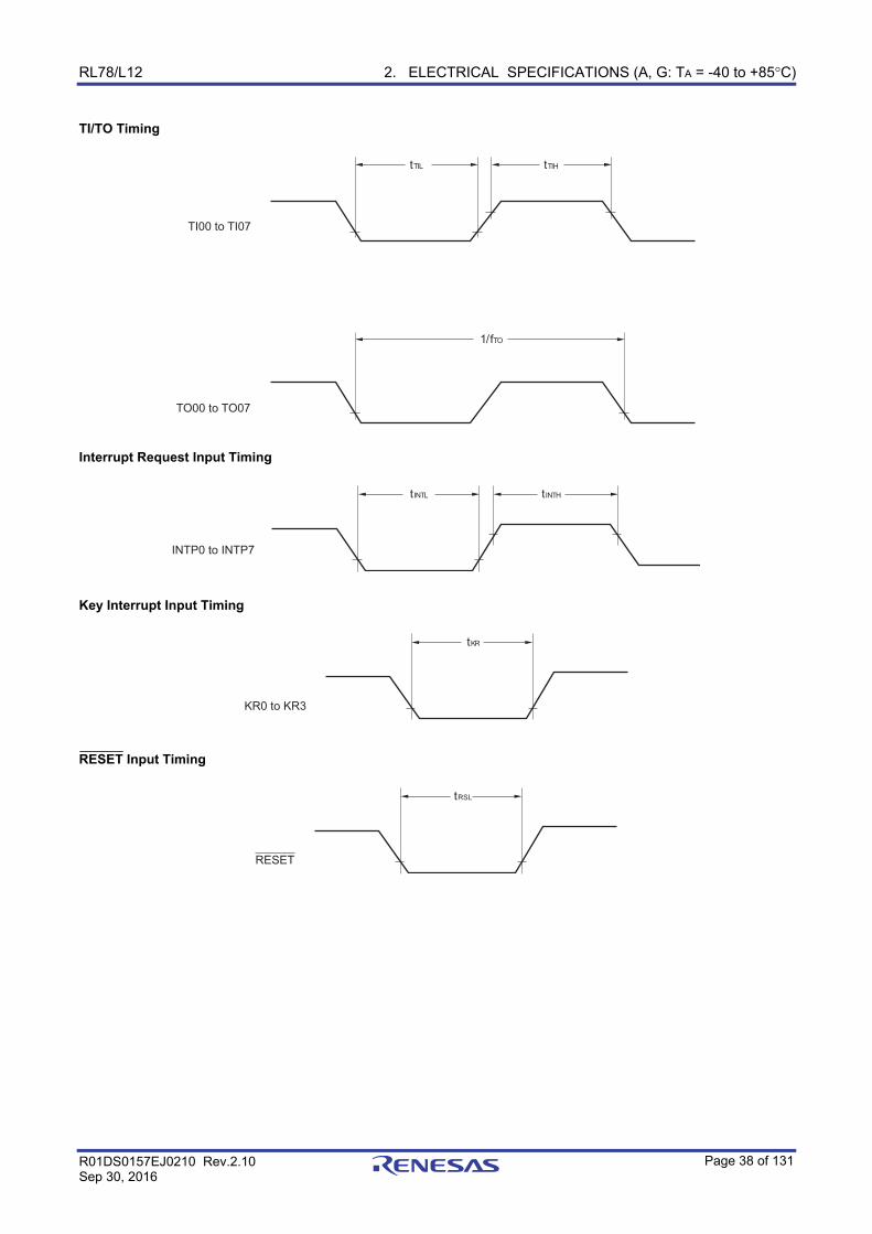
tINTH, tINTL
INTP0 1.6 V ≤ VDD ≤ 5.5 V 1 μs
INTP1 to INTP7 1.6 V ≤ EVDD ≤ 5.5 V 1 μs
Key interrupt input low-level width tKR KR0 to KR3 1.8 V ≤ EVDD ≤ 5.5 V 250 ns 1.6 V ≤ EVDD < 1.8 V 1 μs
RESET low-level width tRSL 10 μs
Remark fMCK: Timer array unit operation clock frequency
(Operation clock to be set by the CKS0n bit of timer mode register 0n (TMR0n). n: Channel number (n = 0 to 7))
RL78/L12 2. ELECTRICAL SPECIFICATIONS (A, G: TA = -40 to +85°C)
R01DS0157EJ0210 Rev.2.10 Sep 30, 2016
Page 36 of 131
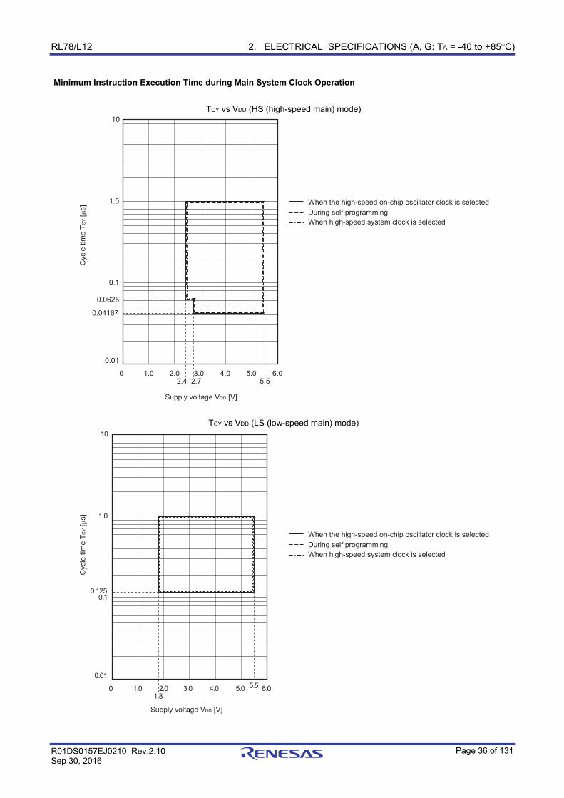
Minimum Instruction Execution Time during Main System Clock Operation
TCY vs VDD (HS (high-speed main) mode)
When the high-speed on-chip oscillator clock is selected
During self programming
When high-speed system clock is selected
Cycle
tim
e T
CY [µ
s]
Supply voltage VDD [V]
1.0
0.1
0
10
1.0 2.0 3.0 4.0 5.0 6.05.52.7
0.01
2.4
0.04167
0.0625
TCY vs VDD (LS (low-speed main) mode)
1.0
0.1
0
10
1.0 2.0 3.0 4.0 5.0 6.05.5
0.01
1.8
0.125
When the high-speed on-chip oscillator clock is selected
During self programming
When high-speed system clock is selected
Cycle
tim
e T
CY [µ
s]
Supply voltage VDD [V]
RL78/L12 2. ELECTRICAL SPECIFICATIONS (A, G: TA = -40 to +85°C)
R01DS0157EJ0210 Rev.2.10 Sep 30, 2016
Page 37 of 131
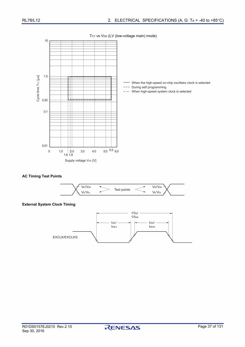
TCY vs VDD (LV (low-voltage main) mode)
1.0
0.1
0
10
1.0 2.0 3.0 4.0 5.0 6.05.5
0.01
1.8
0.25
1.6
When the high-speed on-chip oscillator clock is selected
During self programming
When high-speed system clock is selected
Cycle
tim
e T
CY [µ
s]
Supply voltage VDD [V]
AC Timing Test Points
VIH/VOH
VIL/VOL
Test pointsVIH/VOH
VIL/VOL
External System Clock Timing
EXCLK/EXCLKS
1/fEX/
1/fEXS
tEXL/
tEXLS
tEXH/
tEXHS
RL78/L12 2. ELECTRICAL SPECIFICATIONS (A, G: TA = -40 to +85°C)
R01DS0157EJ0210 Rev.2.10 Sep 30, 2016
Page 38 of 131
TI/TO Timing
TI00 to TI07
tTIL tTIH
TO00 to TO07
1/fTO
Interrupt Request Input Timing
INTP0 to INTP7
tINTL tINTH
Key Interrupt Input Timing
KR0 to KR3
tKR
RESET Input Timing
RESET
tRSL
RL78/L12 2. ELECTRICAL SPECIFICATIONS (A, G: TA = -40 to +85°C)
R01DS0157EJ0210 Rev.2.10 Sep 30, 2016
Page 39 of 131
2.5 Peripheral Functions Characteristics AC Timing Test Points
VIH/VOH
VIL/VOL
Test pointsVIH/VOH
VIL/VOL
2.5.1 Serial array unit (1) During communication at same potential (UART mode)
(TA = −40 to +85°C, 1.6 V ≤ EVDD = VDD ≤ 5.5 V, VSS = EVSS = 0 V)
Parameter Symbol Conditions HS (high-speed
main) Mode
LS (low-speed
main) Mode
LV (low-voltage
main) Mode
Unit
MIN. MAX. MIN. MAX. MIN. MAX.
Transfer rate Note 1 2.4 V ≤ EVDD = VDD ≤ 5.5 V fMCK/6 fMCK/6 fMCK/6 bps
Theoretical value of the
maximum transfer rate
fMCK = fCLK Note 2
4.0 1.3 0.6 Mbps
1.8 V ≤ EVDD = VDD ≤ 5.5 V fMCK/6 fMCK/6 bps
Theoretical value of the
maximum transfer rate
fMCK = fCLK Note 2
1.3 0.6 Mbps
1.6 V ≤ EVDD = VDD ≤ 5.5 V fMCK/6 bps
Theoretical value of the
maximum transfer rate
fMCK = fCLK Note 2
0.6 Mbps
Notes 1. Transfer rate in the SNOOZE mode is 4800 bps only.
2. The maximum operating frequencies of the CPU/peripheral hardware clock (fCLK) are:
HS (high-speed main) mode: 24 MHz (2.7 V ≤ VDD ≤ 5.5 V)
16 MHz (2.4 V ≤ VDD ≤ 5.5 V)
LS (low-speed main) mode: 8 MHz (1.8 V ≤ VDD ≤ 5.5 V)
LV (low-voltage main) mode: 4 MHz (1.6 V ≤ VDD ≤ 5.5 V)
Caution Select the normal input buffer for the RxDq pin and the normal output mode for the TxDq pin by using
port input mode register g (PIMg) and port output mode register g (POMg).
RL78/L12 2. ELECTRICAL SPECIFICATIONS (A, G: TA = -40 to +85°C)
R01DS0157EJ0210 Rev.2.10 Sep 30, 2016
Page 40 of 131
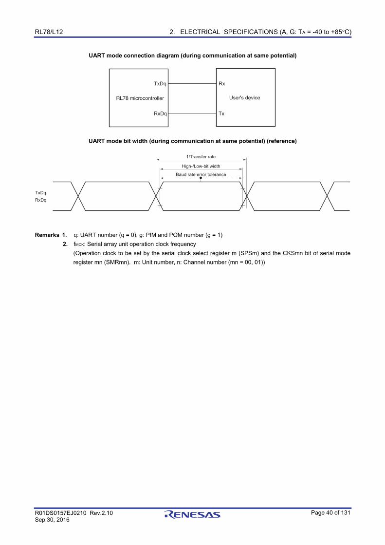
UART mode connection diagram (during communication at same potential)
User's device
TxDq
RxDq
Rx
Tx
RL78 microcontroller
UART mode bit width (during communication at same potential) (reference)
Baud rate error tolerance
High-/Low-bit width
1/Transfer rate
TxDq
RxDq
Remarks 1. q: UART number (q = 0), g: PIM and POM number (g = 1)
2. fMCK: Serial array unit operation clock frequency
(Operation clock to be set by the serial clock select register m (SPSm) and the CKSmn bit of serial mode
register mn (SMRmn). m: Unit number, n: Channel number (mn = 00, 01))
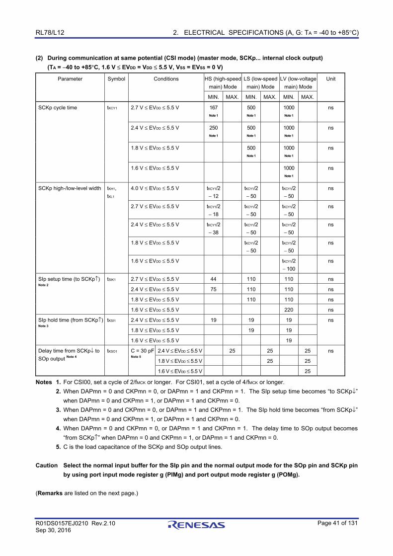
RL78/L12 2. ELECTRICAL SPECIFICATIONS (A, G: TA = -40 to +85°C)
R01DS0157EJ0210 Rev.2.10 Sep 30, 2016
Page 41 of 131
(2) During communication at same potential (CSI mode) (master mode, SCKp... internal clock output) (TA = −40 to +85°C, 1.6 V ≤ EVDD = VDD ≤ 5.5 V, VSS = EVSS = 0 V)
Notes 1. For CSI00, set a cycle of 2/fMCK or longer. For CSI01, set a cycle of 4/fMCK or longer.
2. When DAPmn = 0 and CKPmn = 0, or DAPmn = 1 and CKPmn = 1. The SIp setup time becomes “to SCKp↓”
when DAPmn = 0 and CKPmn = 1, or DAPmn = 1 and CKPmn = 0.
3. When DAPmn = 0 and CKPmn = 0, or DAPmn = 1 and CKPmn = 1. The SIp hold time becomes “from SCKp↓”
when DAPmn = 0 and CKPmn = 1, or DAPmn = 1 and CKPmn = 0.
4. When DAPmn = 0 and CKPmn = 0, or DAPmn = 1 and CKPmn = 1. The delay time to SOp output becomes
“from SCKp↑” when DAPmn = 0 and CKPmn = 1, or DAPmn = 1 and CKPmn = 0.
5. C is the load capacitance of the SCKp and SOp output lines.
Caution Select the normal input buffer for the SIp pin and the normal output mode for the SOp pin and SCKp pin by using port input mode register g (PIMg) and port output mode register g (POMg).
(Remarks are listed on the next page.)
Parameter Symbol Conditions HS (high-speed
main) Mode
LS (low-speed
main) Mode
LV (low-voltage
main) Mode
Unit
MIN. MAX. MIN. MAX. MIN. MAX.
SCKp cycle time tKCY1 2.7 V ≤ EVDD ≤ 5.5 V 167
Note 1
500
Note 1
1000
Note 1
ns
2.4 V ≤ EVDD ≤ 5.5 V 250
Note 1
500
Note 1
1000
Note 1
ns
1.8 V ≤ EVDD ≤ 5.5 V 500
Note 1
1000
Note 1
ns
1.6 V ≤ EVDD ≤ 5.5 V 1000
Note 1
ns
SCKp high-/low-level width tKH1,
tKL1
4.0 V ≤ EVDD ≤ 5.5 V tKCY1/2
− 12
tKCY1/2
− 50
tKCY1/2
− 50
ns
2.7 V ≤ EVDD ≤ 5.5 V tKCY1/2
− 18
tKCY1/2
− 50
tKCY1/2
− 50
ns
2.4 V ≤ EVDD ≤ 5.5 V tKCY1/2
− 38
tKCY1/2
− 50
tKCY1/2
− 50
ns
1.8 V ≤ EVDD ≤ 5.5 V tKCY1/2
− 50
tKCY1/2
− 50
ns
1.6 V ≤ EVDD ≤ 5.5 V tKCY1/2
− 100
ns
SIp setup time (to SCKp↑)
Note 2
tSIK1 2.7 V ≤ EVDD ≤ 5.5 V 44 110 110 ns
2.4 V ≤ EVDD ≤ 5.5 V 75 110 110 ns
1.8 V ≤ EVDD ≤ 5.5 V 110 110 ns
1.6 V ≤ EVDD ≤ 5.5 V 220 ns
SIp hold time (from SCKp↑) Note 3
tKSI1 2.4 V ≤ EVDD ≤ 5.5 V 19 19 19 ns
1.8 V ≤ EVDD ≤ 5.5 V 19 19
1.6 V ≤ EVDD ≤ 5.5 V 19
Delay time from SCKp↓ to
SOp output Note 4
tKSO1 C = 30 pF Note 5
2.4 V ≤ EVDD ≤ 5.5 V 25 25 25 ns
1.8 V ≤ EVDD ≤ 5.5 V 25 25
1.6 V ≤ EVDD ≤ 5.5 V 25
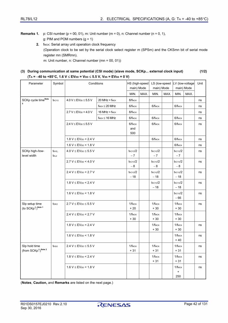
RL78/L12 2. ELECTRICAL SPECIFICATIONS (A, G: TA = -40 to +85°C)
R01DS0157EJ0210 Rev.2.10 Sep 30, 2016
Page 42 of 131
Remarks 1. p: CSI number (p = 00, 01), m: Unit number (m = 0), n: Channel number (n = 0, 1),
g: PIM and POM numbers (g = 1)
2. fMCK: Serial array unit operation clock frequency
(Operation clock to be set by the serial clock select register m (SPSm) and the CKSmn bit of serial mode
register mn (SMRmn).
m: Unit number, n: Channel number (mn = 00, 01))
(3) During communication at same potential (CSI mode) (slave mode, SCKp... external clock input) (1/2) (TA = −40 to +85°C, 1.6 V ≤ EVDD = VDD ≤ 5.5 V, VSS = EVSS = 0 V)
Parameter Symbol Conditions HS (high-speed
main) Mode
LS (low-speed
main) Mode
LV (low-voltage
main) Mode
Unit
MIN. MAX. MIN. MAX. MIN. MAX.
SCKp cycle timeNote
5
tKCY2 4.0 V ≤ EVDD ≤ 5.5 V 20 MHz < fMCK 8/fMCK ns
fMCK ≤ 20 MHz 6/fMCK 6/fMCK 6/fMCK ns
2.7 V ≤ EVDD < 4.0 V 16 MHz < fMCK 8/fMCK ns
fMCK ≤ 16 MHz 6/fMCK 6/fMCK 6/fMCK ns
2.4 V ≤ EVDD ≤ 5.5 V 6/fMCK
and
500
6/fMCK 6/fMCK ns
1.8 V ≤ EVDD < 2.4 V 6/fMCK 6/fMCK ns
1.6 V ≤ EVDD < 1.8 V 6/fMCK ns
SCKp high-/low-
level width
tKH2,
tKL2
4.0 V ≤ EVDD ≤ 5.5 V tKCY2/2
− 7
tKCY2/2
− 7
tKCY2/2
− 7
ns
2.7 V ≤ EVDD < 4.0 V tKCY2/2
− 8
tKCY2/2
− 8
tKCY2/2
− 8
ns
2.4 V ≤ EVDD < 2.7 V tKCY2/2
− 18
tKCY2/2
− 18
tKCY2/2
− 18
ns
1.8 V ≤ EVDD < 2.4 V tKCY2/2
− 18
tKCY2/2
− 18
ns
1.6 V ≤ EVDD < 1.8 V tKCY2/2
− 66
ns
SIp setup time
(to SCKp↑)Note 1
tSIK2 2.7 V ≤ EVDD ≤ 5.5 V 1/fMCK
+ 20
1/fMCK
+ 30
1/fMCK
+ 30
ns
2.4 V ≤ EVDD < 2.7 V 1/fMCK
+ 30
1/fMCK
+ 30
1/fMCK
+ 30
1.8 V ≤ EVDD < 2.4 V 1/fMCK
+ 30
1/fMCK
+ 30
ns
1.6 V ≤ EVDD < 1.8 V 1/fMCK
+ 40
ns
SIp hold time
(from SCKp↑)Note 2
tKSI2 2.4 V ≤ EVDD ≤ 5.5 V 1/fMCK
+ 31
1/fMCK
+ 31
1/fMCK
+ 31
ns
1.8 V ≤ EVDD < 2.4 V 1/fMCK
+ 31
1/fMCK
+ 31
ns
1.6 V ≤ EVDD < 1.8 V 1/fMCK
+
250
ns
(Notes, Caution, and Remarks are listed on the next page.)
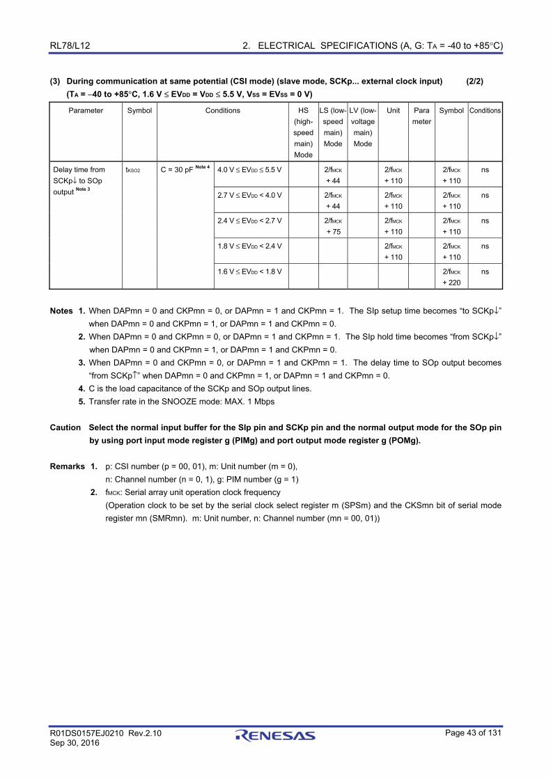
RL78/L12 2. ELECTRICAL SPECIFICATIONS (A, G: TA = -40 to +85°C)
R01DS0157EJ0210 Rev.2.10 Sep 30, 2016
Page 43 of 131
(3) During communication at same potential (CSI mode) (slave mode, SCKp... external clock input) (2/2) (TA = −40 to +85°C, 1.6 V ≤ EVDD = VDD ≤ 5.5 V, VSS = EVSS = 0 V)
Parameter Symbol Conditions HS
(high-
speed
main)
Mode
LS (low-
speed
main)
Mode
LV (low-
voltage
main)
Mode
Unit Para
meter
Symbol Conditions
Delay time from
SCKp↓ to SOp
output Note 3
tKSO2 C = 30 pF Note 4 4.0 V ≤ EVDD ≤ 5.5 V 2/fMCK
+ 44
2/fMCK
+ 110
2/fMCK
+ 110
ns
2.7 V ≤ EVDD < 4.0 V 2/fMCK
+ 44
2/fMCK
+ 110
2/fMCK
+ 110
ns
2.4 V ≤ EVDD < 2.7 V 2/fMCK
+ 75
2/fMCK
+ 110
2/fMCK
+ 110
ns
1.8 V ≤ EVDD < 2.4 V 2/fMCK
+ 110
2/fMCK
+ 110
ns
1.6 V ≤ EVDD < 1.8 V 2/fMCK
+ 220
ns
Notes 1. When DAPmn = 0 and CKPmn = 0, or DAPmn = 1 and CKPmn = 1. The SIp setup time becomes “to SCKp↓”
when DAPmn = 0 and CKPmn = 1, or DAPmn = 1 and CKPmn = 0.
2. When DAPmn = 0 and CKPmn = 0, or DAPmn = 1 and CKPmn = 1. The SIp hold time becomes “from SCKp↓”
when DAPmn = 0 and CKPmn = 1, or DAPmn = 1 and CKPmn = 0.
3. When DAPmn = 0 and CKPmn = 0, or DAPmn = 1 and CKPmn = 1. The delay time to SOp output becomes
“from SCKp↑” when DAPmn = 0 and CKPmn = 1, or DAPmn = 1 and CKPmn = 0.
4. C is the load capacitance of the SCKp and SOp output lines.
5. Transfer rate in the SNOOZE mode: MAX. 1 Mbps
Caution Select the normal input buffer for the SIp pin and SCKp pin and the normal output mode for the SOp pin by using port input mode register g (PIMg) and port output mode register g (POMg).
Remarks 1. p: CSI number (p = 00, 01), m: Unit number (m = 0),
n: Channel number (n = 0, 1), g: PIM number (g = 1)
2. fMCK: Serial array unit operation clock frequency
(Operation clock to be set by the serial clock select register m (SPSm) and the CKSmn bit of serial mode
register mn (SMRmn). m: Unit number, n: Channel number (mn = 00, 01))
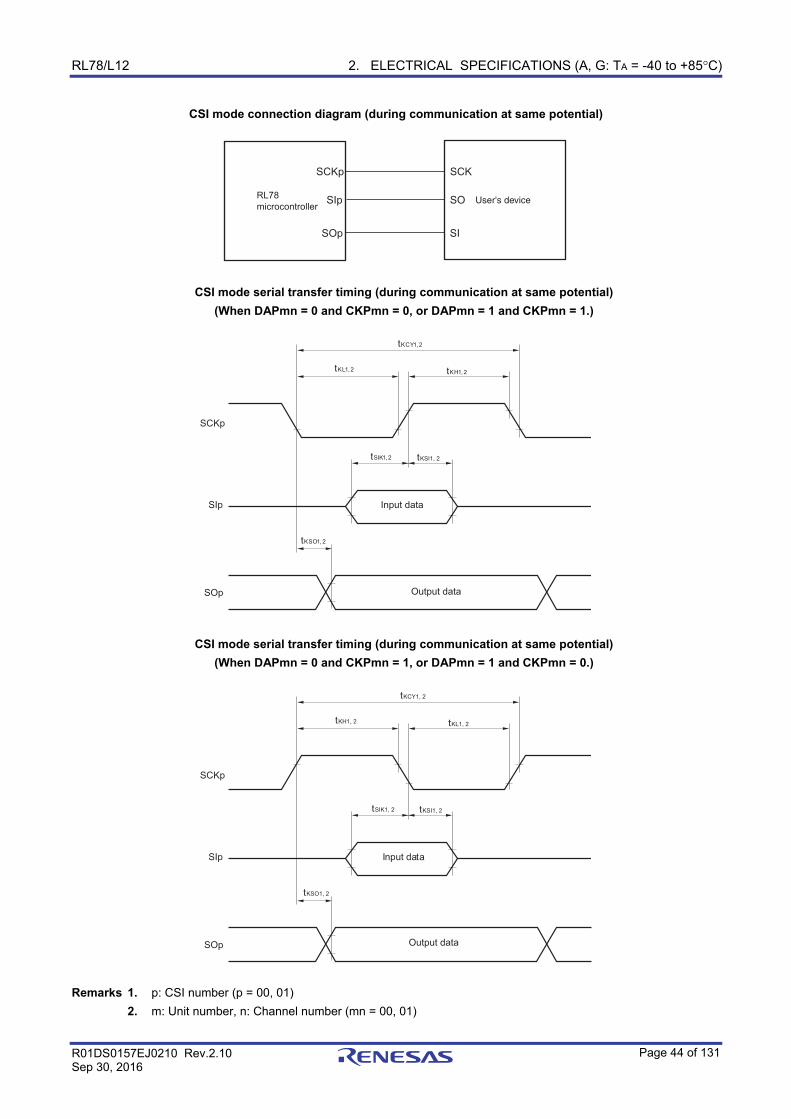
RL78/L12 2. ELECTRICAL SPECIFICATIONS (A, G: TA = -40 to +85°C)
R01DS0157EJ0210 Rev.2.10 Sep 30, 2016
Page 44 of 131
CSI mode connection diagram (during communication at same potential)
RL78
microcontroller
SCKp
SOp
SCK
SI
User's deviceSIp SO
CSI mode serial transfer timing (during communication at same potential) (When DAPmn = 0 and CKPmn = 0, or DAPmn = 1 and CKPmn = 1.)
SIp Input data
Output dataSOp
tKCY1, 2
tKL1, 2 tKH1, 2
tSIK1, 2 tKSI1, 2
tKSO1, 2
SCKp
CSI mode serial transfer timing (during communication at same potential) (When DAPmn = 0 and CKPmn = 1, or DAPmn = 1 and CKPmn = 0.)
SIp Input data
Output dataSOp
tKCY1, 2
tKH1, 2 tKL1, 2
tSIK1, 2 tKSI1, 2
tKSO1, 2
SCKp
Remarks 1. p: CSI number (p = 00, 01)
2. m: Unit number, n: Channel number (mn = 00, 01)
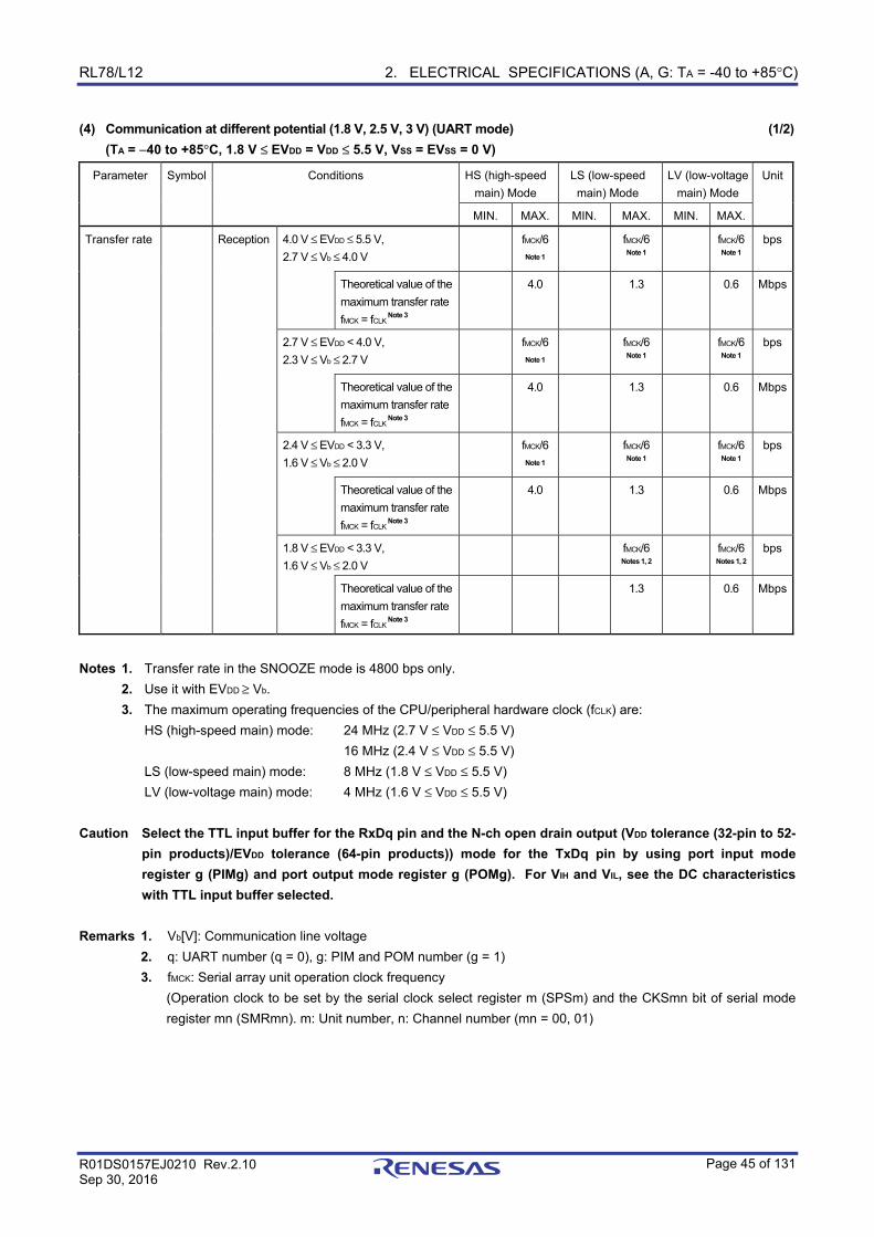
RL78/L12 2. ELECTRICAL SPECIFICATIONS (A, G: TA = -40 to +85°C)
R01DS0157EJ0210 Rev.2.10 Sep 30, 2016
Page 45 of 131
(4) Communication at different potential (1.8 V, 2.5 V, 3 V) (UART mode) (1/2) (TA = −40 to +85°C, 1.8 V ≤ EVDD = VDD ≤ 5.5 V, VSS = EVSS = 0 V)
Parameter Symbol Conditions HS (high-speed
main) Mode
LS (low-speed
main) Mode
LV (low-voltage
main) Mode
Unit
MIN. MAX. MIN. MAX. MIN. MAX.
Transfer rate Reception 4.0 V ≤ EVDD ≤ 5.5 V,
2.7 V ≤ Vb ≤ 4.0 V
fMCK/6 Note 1
fMCK/6 Note 1
fMCK/6Note 1
bps
Theoretical value of the
maximum transfer rate
fMCK = fCLK Note 3
4.0 1.3 0.6 Mbps
2.7 V ≤ EVDD < 4.0 V,
2.3 V ≤ Vb ≤ 2.7 V
fMCK/6 Note 1
fMCK/6 Note 1
fMCK/6Note 1
bps
Theoretical value of the
maximum transfer rate
fMCK = fCLK Note 3
4.0 1.3 0.6 Mbps
2.4 V ≤ EVDD < 3.3 V,
1.6 V ≤ Vb ≤ 2.0 V
fMCK/6 Note 1
fMCK/6 Note 1
fMCK/6Note 1
bps
Theoretical value of the
maximum transfer rate
fMCK = fCLK Note 3
4.0 1.3 0.6 Mbps
1.8 V ≤ EVDD < 3.3 V,
1.6 V ≤ Vb ≤ 2.0 V
fMCK/6 Notes 1, 2
fMCK/6Notes 1, 2
bps
Theoretical value of the
maximum transfer rate
fMCK = fCLK Note 3
1.3 0.6 Mbps
Notes 1. Transfer rate in the SNOOZE mode is 4800 bps only.
2. Use it with EVDD ≥ Vb.
3. The maximum operating frequencies of the CPU/peripheral hardware clock (fCLK) are:
HS (high-speed main) mode: 24 MHz (2.7 V ≤ VDD ≤ 5.5 V)
16 MHz (2.4 V ≤ VDD ≤ 5.5 V)
LS (low-speed main) mode: 8 MHz (1.8 V ≤ VDD ≤ 5.5 V)
LV (low-voltage main) mode: 4 MHz (1.6 V ≤ VDD ≤ 5.5 V)
Caution Select the TTL input buffer for the RxDq pin and the N-ch open drain output (VDD tolerance (32-pin to 52-
pin products)/EVDD tolerance (64-pin products)) mode for the TxDq pin by using port input mode register g (PIMg) and port output mode register g (POMg). For VIH and VIL, see the DC characteristics with TTL input buffer selected.
Remarks 1. Vb[V]: Communication line voltage
2. q: UART number (q = 0), g: PIM and POM number (g = 1)
3. fMCK: Serial array unit operation clock frequency
(Operation clock to be set by the serial clock select register m (SPSm) and the CKSmn bit of serial mode
register mn (SMRmn). m: Unit number, n: Channel number (mn = 00, 01)
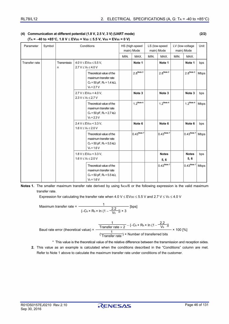
RL78/L12 2. ELECTRICAL SPECIFICATIONS (A, G: TA = -40 to +85°C)
R01DS0157EJ0210 Rev.2.10 Sep 30, 2016
Page 46 of 131
(4) Communication at different potential (1.8 V, 2.5 V, 3 V) (UART mode) (2/2) (TA = −40 to +85°C, 1.8 V ≤ EVDD = VDD ≤ 5.5 V, VSS = EVSS = 0 V)
Parameter Symbol Conditions HS (high-speed
main) Mode
LS (low-speed
main) Mode
LV (low-voltage
main) Mode
Unit
MIN. MAX. MIN. MAX. MIN. MAX.
Transfer rate Transmissio
n
4.0 V ≤ EVDD ≤ 5.5 V,
2.7 V ≤ Vb ≤ 4.0 V
Note 1 Note 1 Note 1 bps
Theoretical value of the
maximum transfer rate
Cb = 50 pF, Rb = 1.4 kΩ,
Vb = 2.7 V
2.8Note 2 2.8Note 2 2.8Note 2 Mbps
2.7 V ≤ EVDD < 4.0 V,
2.3 V ≤ Vb ≤ 2.7 V
Note 3 Note 3 Note 3 bps
Theoretical value of the
maximum transfer rate
Cb = 50 pF, Rb = 2.7 kΩ
Vb = 2.3 V
1.2Note 4 1.2Note 4 1.2Note 4 Mbps
2.4 V ≤ EVDD < 3.3 V,
1.6 V ≤ Vb ≤ 2.0 V
Note 6 Note 6 Note 6 bps
Theoretical value of the
maximum transfer rate
Cb = 50 pF, Rb = 5.5 kΩ
Vb = 1.6 V
0.43Note 7 0.43Note 7 0.43Note 7 Mbps
1.8 V ≤ EVDD < 3.3 V,
1.6 V ≤ Vb ≤ 2.0 V
Notes
5, 6
Notes 5, 6
bps
Theoretical value of the
maximum transfer rate
Cb = 50 pF, Rb = 5.5 kΩ,
Vb = 1.6 V
0.43Note 7 0.43Note 7 Mbps
Notes 1. The smaller maximum transfer rate derived by using fMCK/6 or the following expression is the valid maximum
transfer rate.
Expression for calculating the transfer rate when 4.0 V ≤ EVDD ≤ 5.5 V and 2.7 V ≤ Vb ≤ 4.0 V
Maximum transfer rate = 1
[bps] {−Cb × Rb × ln (1 −
2.2 Vb
)} × 3
1
Transfer rate × 2 − {−Cb × Rb × ln (1 −
2.2 Vb
)}
Baud rate error (theoretical value) =
× 100 [%] (
1 Transfer rate ) × Number of transferred bits
* This value is the theoretical value of the relative difference between the transmission and reception sides.
2. This value as an example is calculated when the conditions described in the “Conditions” column are met.
Refer to Note 1 above to calculate the maximum transfer rate under conditions of the customer.
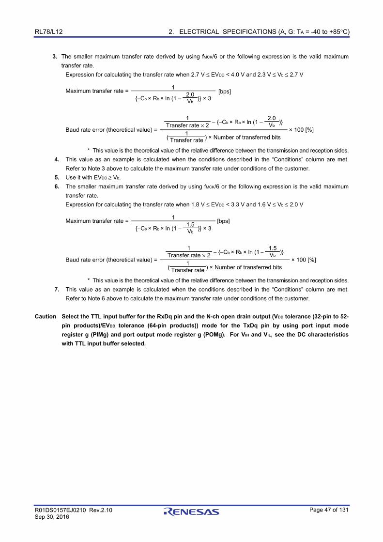
RL78/L12 2. ELECTRICAL SPECIFICATIONS (A, G: TA = -40 to +85°C)
R01DS0157EJ0210 Rev.2.10 Sep 30, 2016
Page 47 of 131
3. The smaller maximum transfer rate derived by using fMCK/6 or the following expression is the valid maximum
transfer rate.
Expression for calculating the transfer rate when 2.7 V ≤ EVDD < 4.0 V and 2.3 V ≤ Vb ≤ 2.7 V
Maximum transfer rate = 1
[bps] {−Cb × Rb × ln (1 −
2.0 Vb
)} × 3
1
Transfer rate × 2 − {−Cb × Rb × ln (1 −
2.0 Vb
)}
Baud rate error (theoretical value) =
× 100 [%] (
1 Transfer rate ) × Number of transferred bits
* This value is the theoretical value of the relative difference between the transmission and reception sides.
4. This value as an example is calculated when the conditions described in the “Conditions” column are met.
Refer to Note 3 above to calculate the maximum transfer rate under conditions of the customer.
5. Use it with EVDD ≥ Vb.
6. The smaller maximum transfer rate derived by using fMCK/6 or the following expression is the valid maximum
transfer rate.
Expression for calculating the transfer rate when 1.8 V ≤ EVDD < 3.3 V and 1.6 V ≤ Vb ≤ 2.0 V
Maximum transfer rate = 1
[bps] {−Cb × Rb × ln (1 −
1.5 Vb
)} × 3
1
Transfer rate × 2 − {−Cb × Rb × ln (1 −
1.5 Vb
)}
Baud rate error (theoretical value) =
× 100 [%] (
1 Transfer rate ) × Number of transferred bits
* This value is the theoretical value of the relative difference between the transmission and reception sides.
7. This value as an example is calculated when the conditions described in the “Conditions” column are met.
Refer to Note 6 above to calculate the maximum transfer rate under conditions of the customer.
Caution Select the TTL input buffer for the RxDq pin and the N-ch open drain output (VDD tolerance (32-pin to 52-
pin products)/EVDD tolerance (64-pin products)) mode for the TxDq pin by using port input mode register g (PIMg) and port output mode register g (POMg). For VIH and VIL, see the DC characteristics with TTL input buffer selected.
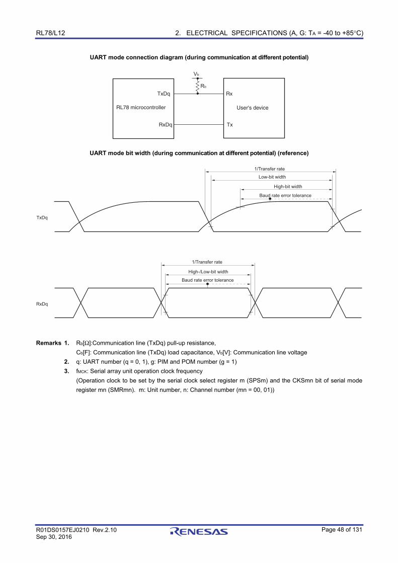
RL78/L12 2. ELECTRICAL SPECIFICATIONS (A, G: TA = -40 to +85°C)
R01DS0157EJ0210 Rev.2.10 Sep 30, 2016
Page 48 of 131
UART mode connection diagram (during communication at different potential)
TxDq
RxDq
Rx
Tx
Vb
Rb
User's deviceRL78 microcontroller
UART mode bit width (during communication at different potential) (reference)
TxDq
RxDq
Baud rate error tolerance
Baud rate error tolerance
Low-bit width
High-/Low-bit width
High-bit width
1/Transfer rate
1/Transfer rate
Remarks 1. Rb[Ω]:Communication line (TxDq) pull-up resistance,
Cb[F]: Communication line (TxDq) load capacitance, Vb[V]: Communication line voltage
2. q: UART number (q = 0, 1), g: PIM and POM number (g = 1)
3. fMCK: Serial array unit operation clock frequency
(Operation clock to be set by the serial clock select register m (SPSm) and the CKSmn bit of serial mode
register mn (SMRmn). m: Unit number, n: Channel number (mn = 00, 01))
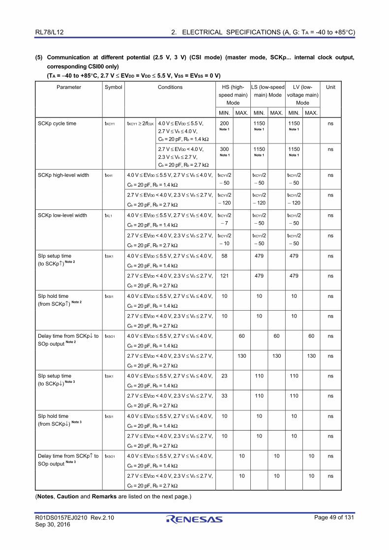
RL78/L12 2. ELECTRICAL SPECIFICATIONS (A, G: TA = -40 to +85°C)
R01DS0157EJ0210 Rev.2.10 Sep 30, 2016
Page 49 of 131
(5) Communication at different potential (2.5 V, 3 V) (CSI mode) (master mode, SCKp... internal clock output, corresponding CSI00 only)
(TA = −40 to +85°C, 2.7 V ≤ EVDD = VDD ≤ 5.5 V, VSS = EVSS = 0 V)
Parameter Symbol Conditions HS (high-
speed main)
Mode
LS (low-speed
main) Mode
LV (low-
voltage main)
Mode
Unit
MIN. MAX. MIN. MAX. MIN. MAX.
SCKp cycle time tKCY1 tKCY1 ≥ 2/fCLK 4.0 V ≤ EVDD ≤ 5.5 V,
2.7 V ≤ Vb ≤ 4.0 V,
Cb = 20 pF, Rb = 1.4 kΩ
200 Note 1
1150 Note 1
1150 Note 1
ns
2.7 V ≤ EVDD < 4.0 V,
2.3 V ≤ Vb ≤ 2.7 V,
Cb = 20 pF, Rb = 2.7 kΩ
300 Note 1
1150Note 1
1150 Note 1
ns
SCKp high-level width tKH1 4.0 V ≤ EVDD ≤ 5.5 V, 2.7 V ≤ Vb ≤ 4.0 V,
Cb = 20 pF, Rb = 1.4 kΩ
tKCY1/2
− 50
tKCY1/2
− 50
tKCY1/2
− 50
ns
2.7 V ≤ EVDD < 4.0 V, 2.3 V ≤ Vb ≤ 2.7 V,
Cb = 20 pF, Rb = 2.7 kΩ
tKCY1/2
− 120
tKCY1/2
− 120
tKCY1/2
− 120
ns
SCKp low-level width tKL1 4.0 V ≤ EVDD ≤ 5.5 V, 2.7 V ≤ Vb ≤ 4.0 V,
Cb = 20 pF, Rb = 1.4 kΩ
tKCY1/2
− 7
tKCY1/2
− 50
tKCY1/2
− 50
ns
2.7 V ≤ EVDD < 4.0 V, 2.3 V ≤ Vb ≤ 2.7 V,
Cb = 20 pF, Rb = 2.7 kΩ
tKCY1/2
− 10
tKCY1/2
− 50
tKCY1/2
− 50
ns
SIp setup time
(to SCKp↑) Note 2
tSIK1 4.0 V ≤ EVDD ≤ 5.5 V, 2.7 V ≤ Vb ≤ 4.0 V,
Cb = 20 pF, Rb = 1.4 kΩ
58 479 479 ns
2.7 V ≤ EVDD < 4.0 V, 2.3 V ≤ Vb ≤ 2.7 V,
Cb = 20 pF, Rb = 2.7 kΩ
121 479 479 ns
SIp hold time
(from SCKp↑) Note 2
tKSI1 4.0 V ≤ EVDD ≤ 5.5 V, 2.7 V ≤ Vb ≤ 4.0 V,
Cb = 20 pF, Rb = 1.4 kΩ
10 10 10 ns
2.7 V ≤ EVDD < 4.0 V, 2.3 V ≤ Vb ≤ 2.7 V,
Cb = 20 pF, Rb = 2.7 kΩ
10 10 10 ns
Delay time from SCKp↓ to
SOp output Note 2
tKSO1 4.0 V ≤ EVDD ≤ 5.5 V, 2.7 V ≤ Vb ≤ 4.0 V,
Cb = 20 pF, Rb = 1.4 kΩ
60 60 60 ns
2.7 V ≤ EVDD < 4.0 V, 2.3 V ≤ Vb ≤ 2.7 V,
Cb = 20 pF, Rb = 2.7 kΩ
130 130 130 ns
SIp setup time
(to SCKp↓) Note 3
tSIK1 4.0 V ≤ EVDD ≤ 5.5 V, 2.7 V ≤ Vb ≤ 4.0 V,
Cb = 20 pF, Rb = 1.4 kΩ
23 110 110 ns
2.7 V ≤ EVDD < 4.0 V, 2.3 V ≤ Vb ≤ 2.7 V,
Cb = 20 pF, Rb = 2.7 kΩ
33 110 110 ns
SIp hold time
(from SCKp↓) Note 3
tKSI1 4.0 V ≤ EVDD ≤ 5.5 V, 2.7 V ≤ Vb ≤ 4.0 V,
Cb = 20 pF, Rb = 1.4 kΩ
10 10 10 ns
2.7 V ≤ EVDD < 4.0 V, 2.3 V ≤ Vb ≤ 2.7 V,
Cb = 20 pF, Rb = 2.7 kΩ
10 10 10 ns
Delay time from SCKp↑ to
SOp output Note 3
tKSO1 4.0 V ≤ EVDD ≤ 5.5 V, 2.7 V ≤ Vb ≤ 4.0 V,
Cb = 20 pF, Rb = 1.4 kΩ
10 10 10 ns
2.7 V ≤ EVDD < 4.0 V, 2.3 V ≤ Vb ≤ 2.7 V,
Cb = 20 pF, Rb = 2.7 kΩ
10 10 10 ns
(Notes, Caution and Remarks are listed on the next page.)
RL78/L12 2. ELECTRICAL SPECIFICATIONS (A, G: TA = -40 to +85°C)
R01DS0157EJ0210 Rev.2.10 Sep 30, 2016
Page 50 of 131
Notes 1. For CSI00, set a cycle of 2/fMCK or longer. For CSI01, set a cycle of 4/fMCK or longer. 2. When DAPmn = 0 and CKPmn = 0, or DAPmn = 1 and CKPmn = 1.
3. When DAPmn = 0 and CKPmn = 1, or DAPmn = 1 and CKPmn = 0.
Caution Select the TTL input buffer for the SIp pin and the N-ch open drain output (VDD tolerance (32-pin to 52-pin products)/EVDD tolerance (64-pin products)) mode for the SOp pin and SCKp pin by using port input mode register g (PIMg) and port output mode register g (POMg). For VIH and VIL, see the DC characteristics with TTL input buffer selected.
Remarks 1. Rb[Ω]:Communication line (SCKp, SOp) pull-up resistance, Cb[F]: Communication line (SCKp, SOp) load
capacitance, Vb[V]: Communication line voltage
2. p: CSI number (p = 00, 01), m: Unit number (m = 0), n: Channel number (n = 0, 1),
g: PIM and POM number (g = 1)
3. fMCK: Serial array unit operation clock frequency
(Operation clock to be set by the serial clock select register m (SPSm) and the CKSmn bit of serial mode
register mn (SMRmn). m: Unit number, n: Channel number (mn = 00, 01)
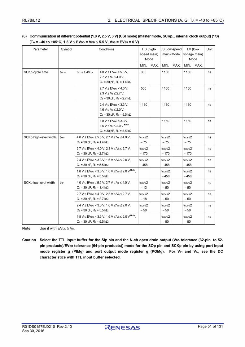
RL78/L12 2. ELECTRICAL SPECIFICATIONS (A, G: TA = -40 to +85°C)
R01DS0157EJ0210 Rev.2.10 Sep 30, 2016
Page 51 of 131
(6) Communication at different potential (1.8 V, 2.5 V, 3 V) (CSI mode) (master mode, SCKp... internal clock output) (1/3) (TA = −40 to +85°C, 1.8 V ≤ EVDD = VDD ≤ 5.5 V, VSS = EVSS = 0 V)
Parameter Symbol Conditions HS (high-
speed main)
Mode
LS (low-speed
main) Mode
LV (low-
voltage main)
Mode
Unit
MIN. MAX. MIN. MAX. MIN. MAX.
SCKp cycle time tKCY1 tKCY1 ≥ 4/fCLK 4.0 V ≤ EVDD ≤ 5.5 V,
2.7 V ≤ Vb ≤ 4.0 V,
Cb = 30 pF, Rb = 1.4 kΩ
300 1150 1150 ns
2.7 V ≤ EVDD < 4.0 V,
2.3 V ≤ Vb ≤ 2.7 V,
Cb = 30 pF, Rb = 2.7 kΩ
500 1150 1150 ns
2.4 V ≤ EVDD < 3.3 V,
1.6 V ≤ Vb ≤ 2.0 V,
Cb = 30 pF, Rb = 5.5 kΩ
1150 1150 1150 ns
1.8 V ≤ EVDD < 3.3 V,
1.6 V ≤ Vb ≤ 2.0 V Note,
Cb = 30 pF, Rb = 5.5 kΩ
1150 1150 ns
SCKp high-level width tKH1 4.0 V ≤ EVDD ≤ 5.5 V, 2.7 V ≤ Vb ≤ 4.0 V,
Cb = 30 pF, Rb = 1.4 kΩ
tKCY1/2
− 75
tKCY1/2
− 75
tKCY1/2
− 75
ns
2.7 V ≤ EVDD < 4.0 V, 2.3 V ≤ Vb ≤ 2.7 V,
Cb = 30 pF, Rb = 2.7 kΩ
tKCY1/2
− 170
tKCY1/2
− 170
tKCY1/2
− 170
ns
2.4 V ≤ EVDD < 3.3 V, 1.6 V ≤ Vb ≤ 2.0 V,
Cb = 30 pF, Rb = 5.5 kΩ
tKCY1/2
− 458
tKCY1/2
− 458
tKCY1/2
− 458
ns
1.8 V ≤ EVDD < 3.3 V, 1.6 V ≤ Vb ≤ 2.0 V Note,
Cb = 30 pF, Rb = 5.5 kΩ
tKCY1/2
− 458
tKCY1/2
− 458
ns
SCKp low-level width tKL1 4.0 V ≤ EVDD ≤ 5.5 V, 2.7 V ≤ Vb ≤ 4.0 V,
Cb = 30 pF, Rb = 1.4 kΩ
tKCY1/2
− 12
tKCY1/2
− 50
tKCY1/2
− 50
ns
2.7 V ≤ EVDD < 4.0 V, 2.3 V ≤ Vb ≤ 2.7 V,
Cb = 30 pF, Rb = 2.7 kΩ
tKCY1/2
− 18
tKCY1/2
− 50
tKCY1/2
− 50
ns
2.4 V ≤ EVDD < 3.3 V, 1.6 V ≤ Vb ≤ 2.0 V,
Cb = 30 pF, Rb = 5.5 kΩ
tKCY1/2
− 50
tKCY1/2
− 50
tKCY1/2
− 50
ns
1.8 V ≤ EVDD < 3.3 V, 1.6 V ≤ Vb ≤ 2.0 V Note,
Cb = 30 pF, Rb = 5.5 kΩ
tKCY1/2
− 50
tKCY1/2
− 50
ns
Note Use it with EVDD ≥ Vb.
Caution Select the TTL input buffer for the SIp pin and the N-ch open drain output (VDD tolerance (32-pin to 52-pin products)/EVDD tolerance (64-pin products)) mode for the SOp pin and SCKp pin by using port input mode register g (PIMg) and port output mode register g (POMg). For VIH and VIL, see the DC characteristics with TTL input buffer selected.
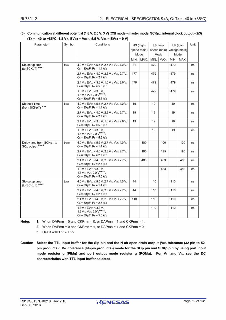
RL78/L12 2. ELECTRICAL SPECIFICATIONS (A, G: TA = -40 to +85°C)
R01DS0157EJ0210 Rev.2.10 Sep 30, 2016
Page 52 of 131
(6) Communication at different potential (1.8 V, 2.5 V, 3 V) (CSI mode) (master mode, SCKp... internal clock output) (2/3) (TA = −40 to +85°C, 1.8 V ≤ EVDD = VDD ≤ 5.5 V, VSS = EVSS = 0 V)
Parameter Symbol Conditions HS (high-
speed main)
Mode
LS (low-
speed main)
Mode
LV (low-
voltage main)
Mode
Unit
MIN. MAX. MIN. MAX. MIN. MAX.
SIp setup time (to SCKp↑) Note 1
tSIK1 4.0 V ≤ EVDD ≤ 5.5 V, 2.7 V ≤ Vb ≤ 4.0 V,Cb = 30 pF, Rb = 1.4 kΩ
81 479 479 ns
2.7 V ≤ EVDD < 4.0 V, 2.3 V ≤ Vb ≤ 2.7 V,Cb = 30 pF, Rb = 2.7 kΩ
177 479 479 ns
2.4 V ≤ EVDD < 3.3 V, 1.6 V ≤ Vb ≤ 2.0 V,Cb = 30 pF, Rb = 5.5 kΩ
479 479 479 ns
1.8 V ≤ EVDD < 3.3 V, 1.6 V ≤ Vb ≤ 2.0 VNote 3, Cb = 30 pF, Rb = 5.5 kΩ
479 479 ns
SIp hold time (from SCKp↑) Note 1
tKSI1 4.0 V ≤ EVDD ≤ 5.5 V, 2.7 V ≤ Vb ≤ 4.0 V,Cb = 30 pF, Rb = 1.4 kΩ
19 19 19 ns
2.7 V ≤ EVDD < 4.0 V, 2.3 V ≤ Vb ≤ 2.7 V,Cb = 30 pF, Rb = 2.7 kΩ
19 19 19 ns
2.4 V ≤ EVDD < 3.3 V, 1.6 V ≤ Vb ≤ 2.0 V,Cb = 30 pF, Rb = 5.5 kΩ
19 19 19 ns
1.8 V ≤ EVDD < 3.3 V, 1.6 V ≤ Vb ≤ 2.0 VNote 3, Cb = 30 pF, Rb = 5.5 kΩ
19 19 ns
Delay time from SCKp↓ to SOp output Note 1
tKSO1 4.0 V ≤ EVDD ≤ 5.5 V, 2.7 V ≤ Vb ≤ 4.0 V,Cb = 30 pF, Rb = 1.4 kΩ
100 100 100 ns
2.7 V ≤ EVDD < 4.0 V, 2.3 V ≤ Vb ≤ 2.7 V,Cb = 30 pF, Rb = 2.7 kΩ
195 195 195 ns
2.4 V ≤ EVDD < 4.0 V, 2.3 V ≤ Vb ≤ 2.7 V,Cb = 30 pF, Rb = 2.7 kΩ
483 483 483 ns
1.8 V ≤ EVDD < 3.3 V, 1.6 V ≤ Vb ≤ 2.0 VNote 3, Cb = 30 pF, Rb = 5.5 kΩ
483 483 ns
SIp setup time (to SCKp↓) Note 2
tSIK1 4.0 V ≤ EVDD ≤ 5.5 V, 2.7 V ≤ Vb ≤ 4.0 V,Cb = 30 pF, Rb = 1.4 kΩ
44 110 110 ns
2.7 V ≤ EVDD < 4.0 V, 2.3 V ≤ Vb ≤ 2.7 V,Cb = 30 pF, Rb = 2.7 kΩ
44 110 110 ns
2.4 V ≤ EVDD < 4.0 V, 2.3 V ≤ Vb ≤ 2.7 V,Cb = 30 pF, Rb = 2.7 kΩ
110 110 110 ns
1.8 V ≤ EVDD < 3.3 V, 1.6 V ≤ Vb ≤ 2.0 VNote 3, Cb = 30 pF, Rb = 5.5 kΩ
110 110 ns
Notes 1. When DAPmn = 0 and CKPmn = 0, or DAPmn = 1 and CKPmn = 1.
2. When DAPmn = 0 and CKPmn = 1, or DAPmn = 1 and CKPmn = 0.
3. Use it with EVDD ≥ Vb. Caution Select the TTL input buffer for the SIp pin and the N-ch open drain output (VDD tolerance (32-pin to 52-
pin products)/EVDD tolerance (64-pin products)) mode for the SOp pin and SCKp pin by using port input mode register g (PIMg) and port output mode register g (POMg). For VIH and VIL, see the DC characteristics with TTL input buffer selected.
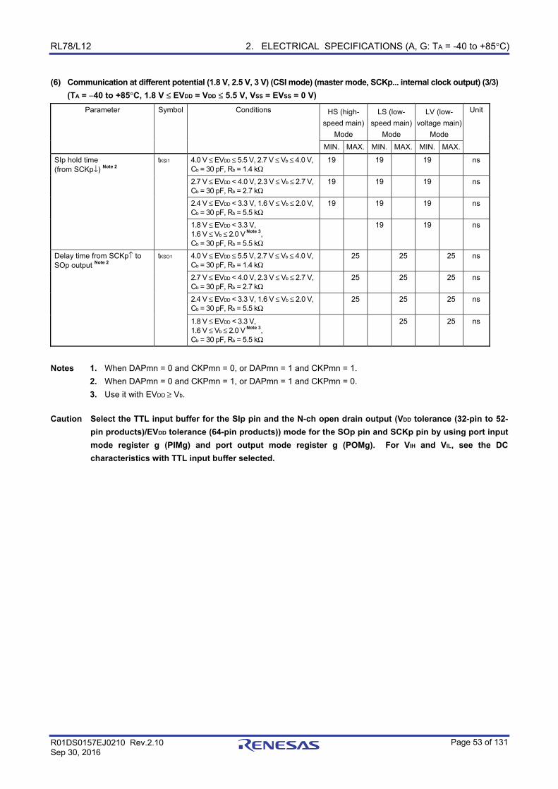
RL78/L12 2. ELECTRICAL SPECIFICATIONS (A, G: TA = -40 to +85°C)
R01DS0157EJ0210 Rev.2.10 Sep 30, 2016
Page 53 of 131
(6) Communication at different potential (1.8 V, 2.5 V, 3 V) (CSI mode) (master mode, SCKp... internal clock output) (3/3) (TA = −40 to +85°C, 1.8 V ≤ EVDD = VDD ≤ 5.5 V, VSS = EVSS = 0 V)
Parameter Symbol Conditions HS (high-
speed main)
Mode
LS (low-
speed main)
Mode
LV (low-
voltage main)
Mode
Unit
MIN. MAX. MIN. MAX. MIN. MAX.
SIp hold time (from SCKp↓) Note 2
tKSI1 4.0 V ≤ EVDD ≤ 5.5 V, 2.7 V ≤ Vb ≤ 4.0 V,Cb = 30 pF, Rb = 1.4 kΩ
19 19 19 ns
2.7 V ≤ EVDD < 4.0 V, 2.3 V ≤ Vb ≤ 2.7 V,Cb = 30 pF, Rb = 2.7 kΩ
19 19 19 ns
2.4 V ≤ EVDD < 3.3 V, 1.6 V ≤ Vb ≤ 2.0 V,Cb = 30 pF, Rb = 5.5 kΩ
19 19 19 ns
1.8 V ≤ EVDD < 3.3 V, 1.6 V ≤ Vb ≤ 2.0 V Note 3, Cb = 30 pF, Rb = 5.5 kΩ
19 19 ns
Delay time from SCKp↑ to SOp output Note 2
tKSO1 4.0 V ≤ EVDD ≤ 5.5 V, 2.7 V ≤ Vb ≤ 4.0 V,Cb = 30 pF, Rb = 1.4 kΩ
25 25 25 ns
2.7 V ≤ EVDD < 4.0 V, 2.3 V ≤ Vb ≤ 2.7 V,Cb = 30 pF, Rb = 2.7 kΩ
25 25 25 ns
2.4 V ≤ EVDD < 3.3 V, 1.6 V ≤ Vb ≤ 2.0 V,Cb = 30 pF, Rb = 5.5 kΩ
25 25 25 ns
1.8 V ≤ EVDD < 3.3 V, 1.6 V ≤ Vb ≤ 2.0 V Note 3, Cb = 30 pF, Rb = 5.5 kΩ
25 25 ns
Notes 1. When DAPmn = 0 and CKPmn = 0, or DAPmn = 1 and CKPmn = 1.
2. When DAPmn = 0 and CKPmn = 1, or DAPmn = 1 and CKPmn = 0.
3. Use it with EVDD ≥ Vb.
Caution Select the TTL input buffer for the SIp pin and the N-ch open drain output (VDD tolerance (32-pin to 52-pin products)/EVDD tolerance (64-pin products)) mode for the SOp pin and SCKp pin by using port input mode register g (PIMg) and port output mode register g (POMg). For VIH and VIL, see the DC characteristics with TTL input buffer selected.
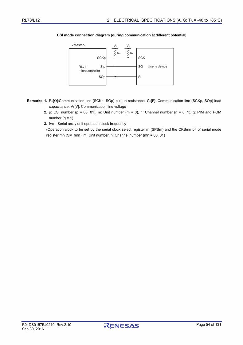
RL78/L12 2. ELECTRICAL SPECIFICATIONS (A, G: TA = -40 to +85°C)
R01DS0157EJ0210 Rev.2.10 Sep 30, 2016
Page 54 of 131
CSI mode connection diagram (during communication at different potential)
Vb
Rb
SCKp
SOp
SCK
SI
User's deviceSIp SO
Vb
Rb
<Master>
RL78microcontroller
Remarks 1. Rb[Ω]:Communication line (SCKp, SOp) pull-up resistance, Cb[F]: Communication line (SCKp, SOp) load
capacitance, Vb[V]: Communication line voltage
2. p: CSI number (p = 00, 01), m: Unit number (m = 0), n: Channel number (n = 0, 1), g: PIM and POM
number (g = 1)
3. fMCK: Serial array unit operation clock frequency
(Operation clock to be set by the serial clock select register m (SPSm) and the CKSmn bit of serial mode
register mn (SMRmn). m: Unit number, n: Channel number (mn = 00, 01)
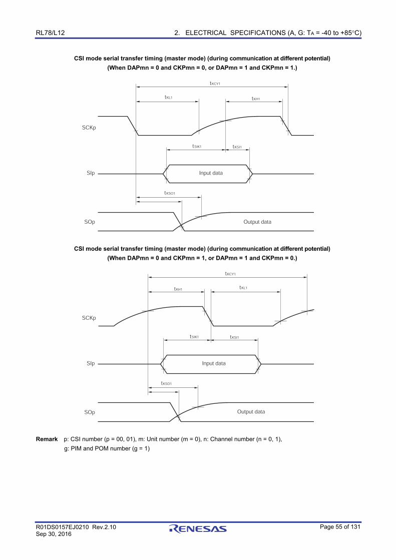
RL78/L12 2. ELECTRICAL SPECIFICATIONS (A, G: TA = -40 to +85°C)
R01DS0157EJ0210 Rev.2.10 Sep 30, 2016
Page 55 of 131
CSI mode serial transfer timing (master mode) (during communication at different potential) (When DAPmn = 0 and CKPmn = 0, or DAPmn = 1 and CKPmn = 1.)
SIp Input data
Output dataSOp
tKCY1
tKL1 tKH1
tSIK1 tKSI1
tKSO1
SCKp
CSI mode serial transfer timing (master mode) (during communication at different potential) (When DAPmn = 0 and CKPmn = 1, or DAPmn = 1 and CKPmn = 0.)
SIp Input data
Output dataSOp
tKCY1
tKL1tKH1
tSIK1 tKSI1
tKSO1
SCKp
Remark p: CSI number (p = 00, 01), m: Unit number (m = 0), n: Channel number (n = 0, 1),
g: PIM and POM number (g = 1)
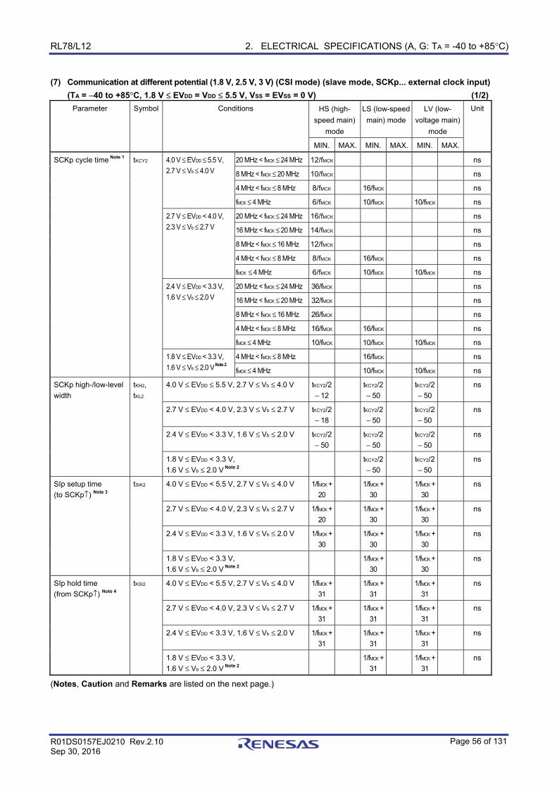
RL78/L12 2. ELECTRICAL SPECIFICATIONS (A, G: TA = -40 to +85°C)
R01DS0157EJ0210 Rev.2.10 Sep 30, 2016
Page 56 of 131
(7) Communication at different potential (1.8 V, 2.5 V, 3 V) (CSI mode) (slave mode, SCKp... external clock input) (TA = −40 to +85°C, 1.8 V ≤ EVDD = VDD ≤ 5.5 V, VSS = EVSS = 0 V) (1/2)
Parameter Symbol Conditions HS (high-
speed main)
mode
LS (low-speed
main) mode
LV (low-
voltage main)
mode
Unit
MIN. MAX. MIN. MAX. MIN. MAX.
SCKp cycle time Note 1 tKCY2 4.0 V ≤ EVDD ≤ 5.5 V,
2.7 V ≤ Vb ≤ 4.0 V
20 MHz < fMCK ≤ 24 MHz 12/fMCK ns
8 MHz < fMCK ≤ 20 MHz 10/fMCK ns
4 MHz < fMCK ≤ 8 MHz 8/fMCK 16/fMCK ns
fMCK ≤ 4 MHz 6/fMCK 10/fMCK 10/fMCK ns
2.7 V ≤ EVDD < 4.0 V,
2.3 V ≤ Vb ≤ 2.7 V
20 MHz < fMCK ≤ 24 MHz 16/fMCK ns
16 MHz < fMCK ≤ 20 MHz 14/fMCK ns
8 MHz < fMCK ≤ 16 MHz 12/fMCK ns
4 MHz < fMCK ≤ 8 MHz 8/fMCK 16/fMCK ns
fMCK ≤ 4 MHz 6/fMCK 10/fMCK 10/fMCK ns
2.4 V ≤ EVDD < 3.3 V,
1.6 V ≤ Vb ≤ 2.0 V
20 MHz < fMCK ≤ 24 MHz 36/fMCK ns
16 MHz < fMCK ≤ 20 MHz 32/fMCK ns
8 MHz < fMCK ≤ 16 MHz 26/fMCK ns
4 MHz < fMCK ≤ 8 MHz 16/fMCK 16/fMCK ns
fMCK ≤ 4 MHz 10/fMCK 10/fMCK 10/fMCK ns
1.8 V ≤ EVDD < 3.3 V,
1.6 V ≤ Vb ≤ 2.0 V Note 2
4 MHz < fMCK ≤ 8 MHz 16/fMCK ns
fMCK ≤ 4 MHz 10/fMCK 10/fMCK ns
SCKp high-/low-level
width
tKH2,
tKL2
4.0 V ≤ EVDD ≤ 5.5 V, 2.7 V ≤ Vb ≤ 4.0 V tKCY2/2
− 12
tKCY2/2
− 50
tKCY2/2
− 50
ns
2.7 V ≤ EVDD < 4.0 V, 2.3 V ≤ Vb ≤ 2.7 V tKCY2/2
− 18
tKCY2/2
− 50
tKCY2/2
− 50
ns
2.4 V ≤ EVDD < 3.3 V, 1.6 V ≤ Vb ≤ 2.0 V tKCY2/2
− 50
tKCY2/2
− 50
tKCY2/2
− 50
ns
1.8 V ≤ EVDD < 3.3 V,
1.6 V ≤ Vb ≤ 2.0 V Note 2
tKCY2/2
− 50
tKCY2/2
− 50
ns
SIp setup time
(to SCKp↑) Note 3
tSIK2 4.0 V ≤ EVDD < 5.5 V, 2.7 V ≤ Vb ≤ 4.0 V 1/fMCK +
20
1/fMCK +
30
1/fMCK +
30
ns
2.7 V ≤ EVDD < 4.0 V, 2.3 V ≤ Vb ≤ 2.7 V 1/fMCK +
20
1/fMCK +
30
1/fMCK +
30
ns
2.4 V ≤ EVDD < 3.3 V, 1.6 V ≤ Vb ≤ 2.0 V 1/fMCK +
30
1/fMCK +
30
1/fMCK +
30
ns
1.8 V ≤ EVDD < 3.3 V,
1.6 V ≤ Vb ≤ 2.0 V Note 2
1/fMCK +
30
1/fMCK +
30
ns
SIp hold time
(from SCKp↑) Note 4
tKSI2 4.0 V ≤ EVDD < 5.5 V, 2.7 V ≤ Vb ≤ 4.0 V 1/fMCK +
31
1/fMCK +
31
1/fMCK +
31
ns
2.7 V ≤ EVDD < 4.0 V, 2.3 V ≤ Vb ≤ 2.7 V 1/fMCK +
31
1/fMCK +
31
1/fMCK +
31
ns
2.4 V ≤ EVDD < 3.3 V, 1.6 V ≤ Vb ≤ 2.0 V 1/fMCK +
31
1/fMCK +
31
1/fMCK +
31
ns
1.8 V ≤ EVDD < 3.3 V,
1.6 V ≤ Vb ≤ 2.0 V Note 2
1/fMCK +
31
1/fMCK +
31
ns
(Notes, Caution and Remarks are listed on the next page.)
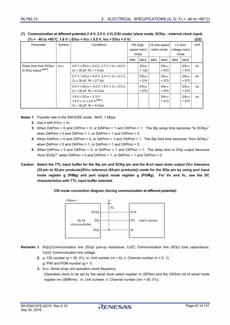
RL78/L12 2. ELECTRICAL SPECIFICATIONS (A, G: TA = -40 to +85°C)
R01DS0157EJ0210 Rev.2.10 Sep 30, 2016
Page 57 of 131
(7) Communication at different potential (1.8 V, 2.5 V, 3 V) (CSI mode) (slave mode, SCKp... external clock input) (TA = −40 to +85°C, 1.8 V ≤ EVDD = VDD ≤ 5.5 V, VSS = EVSS = 0 V) (2/2)
Parameter Symbol Conditions HS (high-
speed main)
mode
LS (low-speed
main) mode
LV (low-
voltage main)
mode
Unit
MIN. MAX. MIN. MAX. MIN. MAX.
Delay time from SCKp↓
to SOp output Note 5
tKSO2 4.0 V ≤ EVDD ≤ 5.5 V, 2.7 V ≤ Vb ≤ 4.0 V,
Cb = 30 pF, Rb = 1.4 kΩ
2/fMCK
+ 120
2/fMCK
+ 573
2/fMCK
+ 573
ns
2.7 V ≤ EVDD < 4.0 V, 2.3 V ≤ Vb ≤ 2.7 V,
Cb = 30 pF, Rb = 2.7 kΩ
2/fMCK
+ 214
2/fMCK
+ 573
2/fMCK
+ 573
ns
2.4 V ≤ EVDD < 3.3 V, 1.6 V ≤ Vb ≤ 2.0 V,
Cb = 30 pF, Rb = 5.5 kΩ
2/fMCK
+ 573
2/fMCK
+ 573
2/fMCK
+ 573
ns
1.8 V ≤ EVDD < 3.3 V,
1.6 V ≤ Vb ≤ 2.0 V Note 2,
Cb = 30 pF, Rb = 5.5 kΩ
2/fMCK
+ 573
2/fMCK
+ 573
ns
Notes 1. Transfer rate in the SNOOZE mode : MAX. 1 Mbps
2. Use it with EVDD ≥ Vb. 3. When DAPmn = 0 and CKPmn = 0, or DAPmn = 1 and CKPmn = 1. The SIp setup time becomes “to SCKp↓”
when DAPmn = 0 and CKPmn = 1, or DAPmn = 1 and CKPmn = 0.
4. When DAPmn = 0 and CKPmn = 0, or DAPmn = 1 and CKPmn = 1. The SIp hold time becomes “from SCKp↓”
when DAPmn = 0 and CKPmn = 1, or DAPmn = 1 and CKPmn = 0.
5. When DAPmn = 0 and CKPmn = 0, or DAPmn = 1 and CKPmn = 1. The delay time to SOp output becomes
“from SCKp↑” when DAPmn = 0 and CKPmn = 1, or DAPmn = 1 and CKPmn = 0.
Caution Select the TTL input buffer for the SIp pin and SCKp pin and the N-ch open drain output (VDD tolerance (32-pin to 52-pin products)/EVDD tolerance (64-pin products)) mode for the SOp pin by using port input mode register g (PIMg) and port output mode register g (POMg). For VIH and VIL, see the DC characteristics with TTL input buffer selected.
CSI mode connection diagram (during communication at different potential)
User's device
<Slave>
SCKp
SOp
SCK
SI
SIp SO
Vb
Rb
RL78microcontroller
Remarks 1. Rb[Ω]:Communication line (SOp) pull-up resistance, Cb[F]: Communication line (SOp) load capacitance,
Vb[V]: Communication line voltage
2. p: CSI number (p = 00, 01), m: Unit number (m = 0), n: Channel number (n = 0, 1),
g: PIM and POM number (g = 1)
3. fMCK: Serial array unit operation clock frequency
(Operation clock to be set by the serial clock select register m (SPSm) and the CKSmn bit of serial mode
register mn (SMRmn). m: Unit number, n: Channel number (mn = 00, 01))
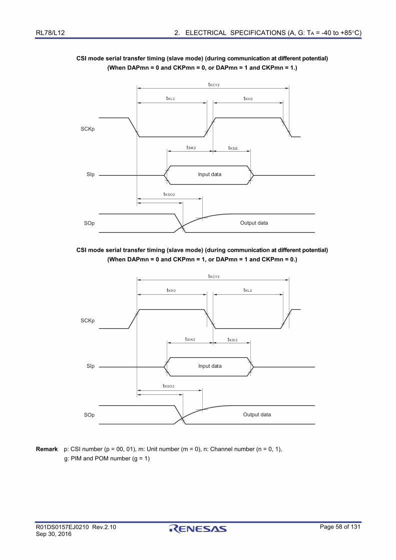
RL78/L12 2. ELECTRICAL SPECIFICATIONS (A, G: TA = -40 to +85°C)
R01DS0157EJ0210 Rev.2.10 Sep 30, 2016
Page 58 of 131
CSI mode serial transfer timing (slave mode) (during communication at different potential) (When DAPmn = 0 and CKPmn = 0, or DAPmn = 1 and CKPmn = 1.)
SIp Input data
Output dataSOp
tKCY2
tKL2 tKH2
tSIK2 tKSI2
tKSO2
SCKp
CSI mode serial transfer timing (slave mode) (during communication at different potential) (When DAPmn = 0 and CKPmn = 1, or DAPmn = 1 and CKPmn = 0.)
SIp Input data
Output dataSOp
tKCY2
tKL2tKH2
tSI K2 tKSI 2
tKSO2
SCKp
Remark p: CSI number (p = 00, 01), m: Unit number (m = 0), n: Channel number (n = 0, 1),
g: PIM and POM number (g = 1)
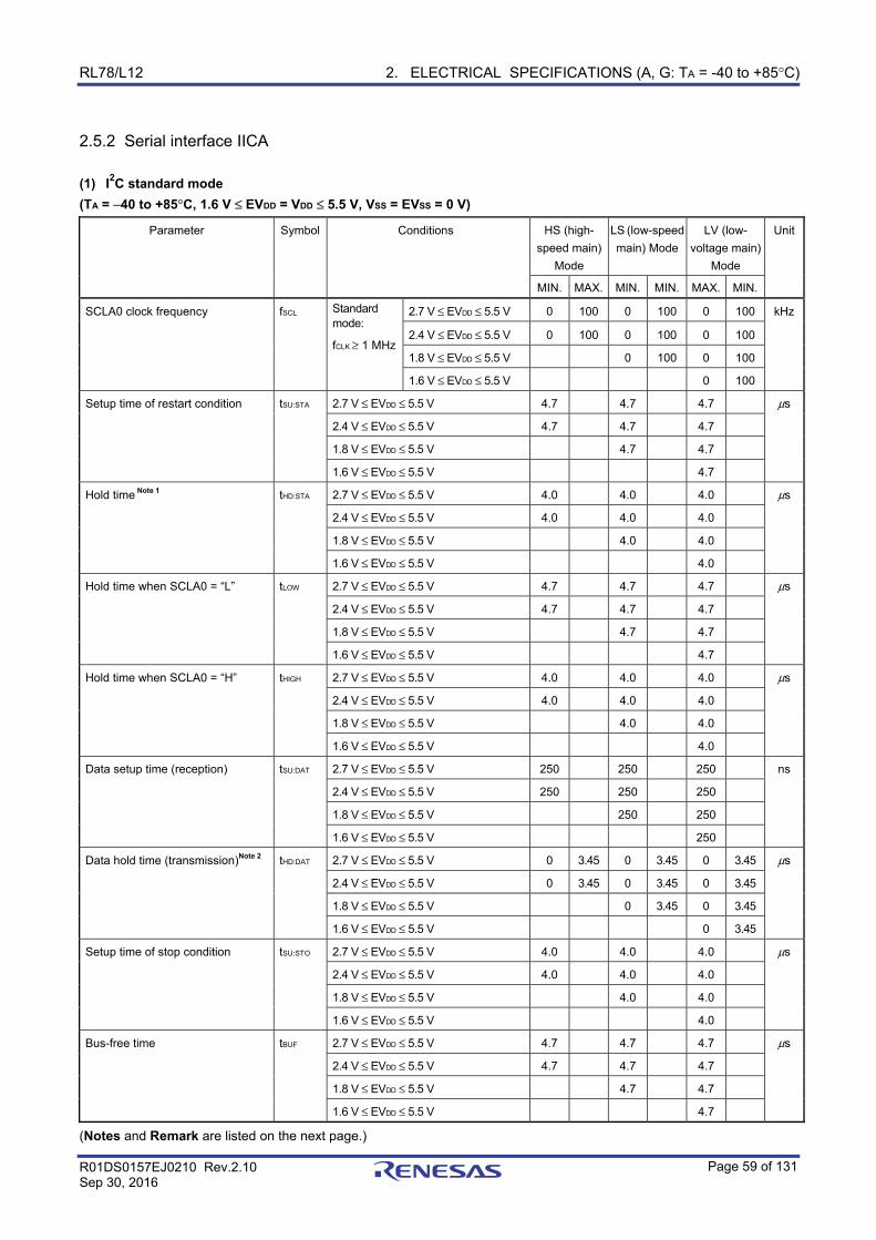
RL78/L12 2. ELECTRICAL SPECIFICATIONS (A, G: TA = -40 to +85°C)
R01DS0157EJ0210 Rev.2.10 Sep 30, 2016
Page 59 of 131
2.5.2 Serial interface IICA (1) I2C standard mode (TA = −40 to +85°C, 1.6 V ≤ EVDD = VDD ≤ 5.5 V, VSS = EVSS = 0 V)
Parameter Symbol Conditions HS (high-
speed main)
Mode
LS (low-speed
main) Mode
LV (low-
voltage main)
Mode
Unit
MIN. MAX. MIN. MIN. MAX. MIN.
SCLA0 clock frequency fSCL Standard mode:
fCLK ≥ 1 MHz
2.7 V ≤ EVDD ≤ 5.5 V 0 100 0 100 0 100 kHz
2.4 V ≤ EVDD ≤ 5.5 V 0 100 0 100 0 100
1.8 V ≤ EVDD ≤ 5.5 V 0 100 0 100
1.6 V ≤ EVDD ≤ 5.5 V 0 100
Setup time of restart condition tSU:STA 2.7 V ≤ EVDD ≤ 5.5 V 4.7 4.7 4.7 μs
2.4 V ≤ EVDD ≤ 5.5 V 4.7 4.7 4.7
1.8 V ≤ EVDD ≤ 5.5 V 4.7 4.7
1.6 V ≤ EVDD ≤ 5.5 V 4.7
Hold time Note 1 tHD:STA 2.7 V ≤ EVDD ≤ 5.5 V 4.0 4.0 4.0 μs
2.4 V ≤ EVDD ≤ 5.5 V 4.0 4.0 4.0
1.8 V ≤ EVDD ≤ 5.5 V 4.0 4.0
1.6 V ≤ EVDD ≤ 5.5 V 4.0
Hold time when SCLA0 = “L” tLOW 2.7 V ≤ EVDD ≤ 5.5 V 4.7 4.7 4.7 μs
2.4 V ≤ EVDD ≤ 5.5 V 4.7 4.7 4.7
1.8 V ≤ EVDD ≤ 5.5 V 4.7 4.7
1.6 V ≤ EVDD ≤ 5.5 V 4.7
Hold time when SCLA0 = “H” tHIGH 2.7 V ≤ EVDD ≤ 5.5 V 4.0 4.0 4.0 μs
2.4 V ≤ EVDD ≤ 5.5 V 4.0 4.0 4.0
1.8 V ≤ EVDD ≤ 5.5 V 4.0 4.0
1.6 V ≤ EVDD ≤ 5.5 V 4.0
Data setup time (reception) tSU:DAT 2.7 V ≤ EVDD ≤ 5.5 V 250 250 250 ns
2.4 V ≤ EVDD ≤ 5.5 V 250 250 250
1.8 V ≤ EVDD ≤ 5.5 V 250 250
1.6 V ≤ EVDD ≤ 5.5 V 250
Data hold time (transmission)Note 2 tHD:DAT 2.7 V ≤ EVDD ≤ 5.5 V 0 3.45 0 3.45 0 3.45 μs
2.4 V ≤ EVDD ≤ 5.5 V 0 3.45 0 3.45 0 3.45
1.8 V ≤ EVDD ≤ 5.5 V 0 3.45 0 3.45
1.6 V ≤ EVDD ≤ 5.5 V 0 3.45
Setup time of stop condition tSU:STO 2.7 V ≤ EVDD ≤ 5.5 V 4.0 4.0 4.0 μs
2.4 V ≤ EVDD ≤ 5.5 V 4.0 4.0 4.0
1.8 V ≤ EVDD ≤ 5.5 V 4.0 4.0
1.6 V ≤ EVDD ≤ 5.5 V 4.0
Bus-free time tBUF 2.7 V ≤ EVDD ≤ 5.5 V 4.7 4.7 4.7 μs
2.4 V ≤ EVDD ≤ 5.5 V 4.7 4.7 4.7
1.8 V ≤ EVDD ≤ 5.5 V 4.7 4.7
1.6 V ≤ EVDD ≤ 5.5 V 4.7
(Notes and Remark are listed on the next page.)
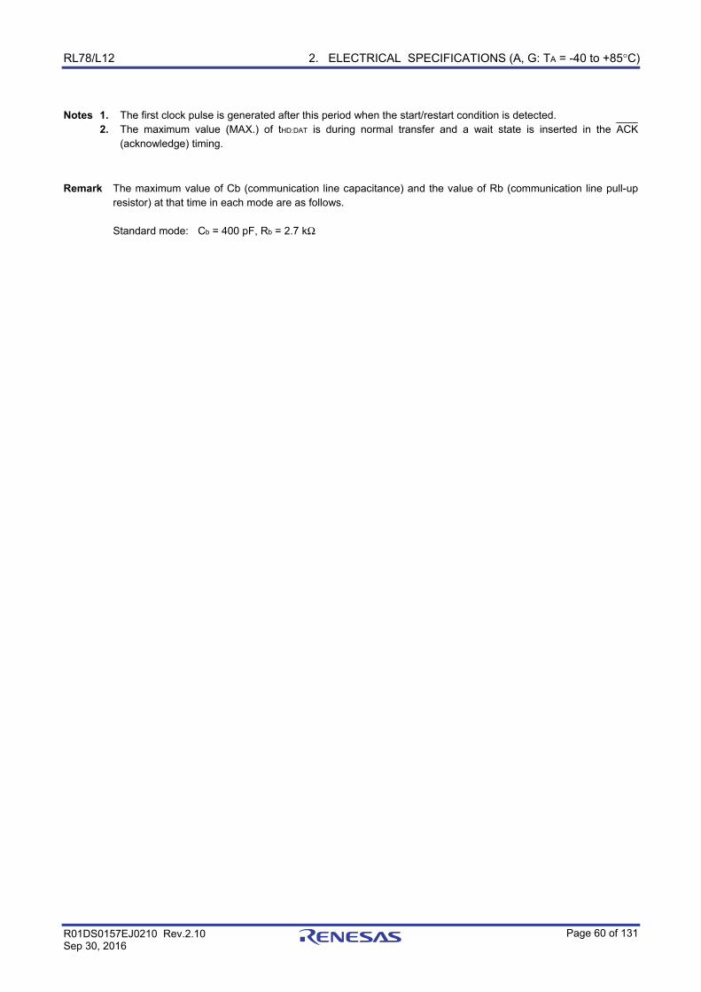
RL78/L12 2. ELECTRICAL SPECIFICATIONS (A, G: TA = -40 to +85°C)
R01DS0157EJ0210 Rev.2.10 Sep 30, 2016
Page 60 of 131
Notes 1. The first clock pulse is generated after this period when the start/restart condition is detected. 2. The maximum value (MAX.) of tHD:DAT is during normal transfer and a wait state is inserted in the ACK
(acknowledge) timing.
Remark The maximum value of Cb (communication line capacitance) and the value of Rb (communication line pull-up
resistor) at that time in each mode are as follows. Standard mode: Cb = 400 pF, Rb = 2.7 kΩ
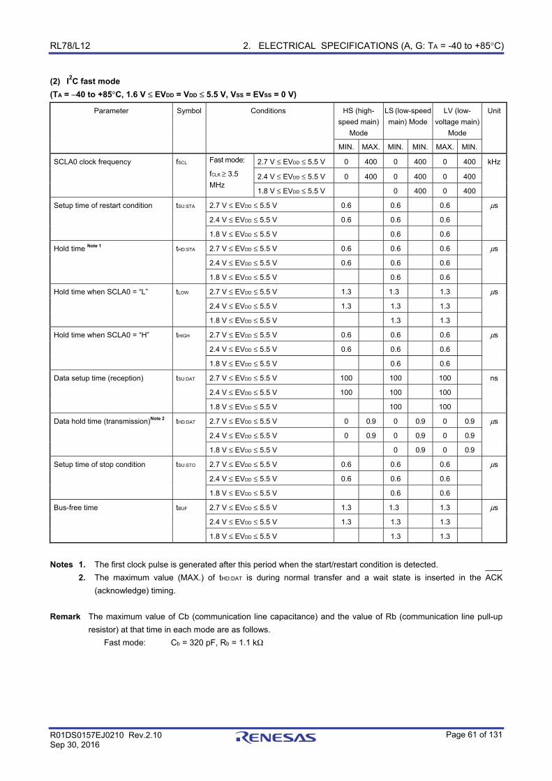
RL78/L12 2. ELECTRICAL SPECIFICATIONS (A, G: TA = -40 to +85°C)
R01DS0157EJ0210 Rev.2.10 Sep 30, 2016
Page 61 of 131
(2) I2C fast mode (TA = −40 to +85°C, 1.6 V ≤ EVDD = VDD ≤ 5.5 V, VSS = EVSS = 0 V)
Parameter Symbol Conditions HS (high-
speed main)
Mode
LS (low-speed
main) Mode
LV (low-
voltage main)
Mode
Unit
MIN. MAX. MIN. MIN. MAX. MIN.
SCLA0 clock frequency fSCL Fast mode:
fCLK ≥ 3.5
MHz
2.7 V ≤ EVDD ≤ 5.5 V 0 400 0 400 0 400 kHz
2.4 V ≤ EVDD ≤ 5.5 V 0 400 0 400 0 400
1.8 V ≤ EVDD ≤ 5.5 V 0 400 0 400
Setup time of restart condition tSU:STA 2.7 V ≤ EVDD ≤ 5.5 V 0.6 0.6 0.6 μs
2.4 V ≤ EVDD ≤ 5.5 V 0.6 0.6 0.6
1.8 V ≤ EVDD ≤ 5.5 V 0.6 0.6
Hold time Note 1 tHD:STA 2.7 V ≤ EVDD ≤ 5.5 V 0.6 0.6 0.6 μs
2.4 V ≤ EVDD ≤ 5.5 V 0.6 0.6 0.6
1.8 V ≤ EVDD ≤ 5.5 V 0.6 0.6
Hold time when SCLA0 = “L” tLOW 2.7 V ≤ EVDD ≤ 5.5 V 1.3 1.3 1.3 μs
2.4 V ≤ EVDD ≤ 5.5 V 1.3 1.3 1.3
1.8 V ≤ EVDD ≤ 5.5 V 1.3 1.3
Hold time when SCLA0 = “H” tHIGH 2.7 V ≤ EVDD ≤ 5.5 V 0.6 0.6 0.6 μs
2.4 V ≤ EVDD ≤ 5.5 V 0.6 0.6 0.6
1.8 V ≤ EVDD ≤ 5.5 V 0.6 0.6
Data setup time (reception) tSU:DAT 2.7 V ≤ EVDD ≤ 5.5 V 100 100 100 ns
2.4 V ≤ EVDD ≤ 5.5 V 100 100 100
1.8 V ≤ EVDD ≤ 5.5 V 100 100
Data hold time (transmission)Note 2 tHD:DAT 2.7 V ≤ EVDD ≤ 5.5 V 0 0.9 0 0.9 0 0.9 μs
2.4 V ≤ EVDD ≤ 5.5 V 0 0.9 0 0.9 0 0.9
1.8 V ≤ EVDD ≤ 5.5 V 0 0.9 0 0.9
Setup time of stop condition tSU:STO 2.7 V ≤ EVDD ≤ 5.5 V 0.6 0.6 0.6 μs
2.4 V ≤ EVDD ≤ 5.5 V 0.6 0.6 0.6
1.8 V ≤ EVDD ≤ 5.5 V 0.6 0.6
Bus-free time tBUF 2.7 V ≤ EVDD ≤ 5.5 V 1.3 1.3 1.3 μs
2.4 V ≤ EVDD ≤ 5.5 V 1.3 1.3 1.3
1.8 V ≤ EVDD ≤ 5.5 V 1.3 1.3
Notes 1. The first clock pulse is generated after this period when the start/restart condition is detected.
2. The maximum value (MAX.) of tHD:DAT is during normal transfer and a wait state is inserted in the ACK
(acknowledge) timing.
Remark The maximum value of Cb (communication line capacitance) and the value of Rb (communication line pull-up
resistor) at that time in each mode are as follows.
Fast mode: Cb = 320 pF, Rb = 1.1 kΩ
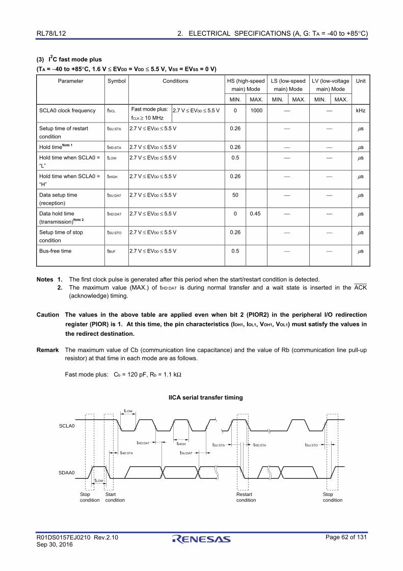
RL78/L12 2. ELECTRICAL SPECIFICATIONS (A, G: TA = -40 to +85°C)
R01DS0157EJ0210 Rev.2.10 Sep 30, 2016
Page 62 of 131
(3) I2C fast mode plus (TA = −40 to +85°C, 1.6 V ≤ EVDD = VDD ≤ 5.5 V, VSS = EVSS = 0 V)
Parameter Symbol Conditions HS (high-speed
main) Mode
LS (low-speed
main) Mode
LV (low-voltage
main) Mode
Unit
MIN. MAX. MIN. MAX. MIN. MAX.
SCLA0 clock frequency fSCL Fast mode plus:
fCLK ≥ 10 MHz 2.7 V ≤ EVDD ≤ 5.5 V 0 1000 ⎯ ⎯ kHz
Setup time of restart
condition
tSU:STA 2.7 V ≤ EVDD ≤ 5.5 V 0.26 ⎯ ⎯ μs
Hold timeNote 1 tHD:STA 2.7 V ≤ EVDD ≤ 5.5 V 0.26 ⎯ ⎯ μs
Hold time when SCLA0 =
“L”
tLOW 2.7 V ≤ EVDD ≤ 5.5 V 0.5 ⎯ ⎯ μs
Hold time when SCLA0 =
“H”
tHIGH 2.7 V ≤ EVDD ≤ 5.5 V 0.26 ⎯ ⎯ μs
Data setup time
(reception)
tSU:DAT 2.7 V ≤ EVDD ≤ 5.5 V 50 ⎯ ⎯ μs
Data hold time
(transmission)Note 2
tHD:DAT 2.7 V ≤ EVDD ≤ 5.5 V 0 0.45 ⎯ ⎯ μs
Setup time of stop
condition
tSU:STO 2.7 V ≤ EVDD ≤ 5.5 V 0.26 ⎯ ⎯ μs
Bus-free time tBUF 2.7 V ≤ EVDD ≤ 5.5 V 0.5 ⎯ ⎯ μs
Notes 1. The first clock pulse is generated after this period when the start/restart condition is detected. 2. The maximum value (MAX.) of tHD:DAT is during normal transfer and a wait state is inserted in the ACK
(acknowledge) timing.
Caution The values in the above table are applied even when bit 2 (PIOR2) in the peripheral I/O redirection register (PIOR) is 1. At this time, the pin characteristics (IOH1, IOL1, VOH1, VOL1) must satisfy the values in the redirect destination.
Remark The maximum value of Cb (communication line capacitance) and the value of Rb (communication line pull-up
resistor) at that time in each mode are as follows. Fast mode plus: Cb = 120 pF, Rb = 1.1 kΩ
IICA serial transfer timing
tLOW
tLOW
tHIGH
tHD:STA
Stop condition
Start condition
Restart condition
Stop condition
tSU:DAT
tSU:STA tSU:STOtHD:STAtHD:DAT
SCLA0
SDAA0
RL78/L12 2. ELECTRICAL SPECIFICATIONS (A, G: TA = -40 to +85°C)
R01DS0157EJ0210 Rev.2.10 Sep 30, 2016
Page 63 of 131
2.6 Analog Characteristics
2.6.1 A/D converter characteristics Classification of A/D converter characteristics
Input channel
Reference Voltage
Reference voltage (+) = AVREFP
Reference voltage (−) = AVREFM
Reference voltage (+) = VDD
Reference voltage (−) = VSS
Reference voltage (+) = VBGR
Reference voltage (−) = AVREFM
ANI0, ANI1 − Refer to 2.6.1 (3). Refer to 2.6.1 (4).
ANI16 to ANI23 Refer to 2.6.1 (2).
Internal reference voltage
Temperature sensor output voltage
Refer to 2.6.1 (1). −
(1) When reference voltage (+) = AVREFP/ANI0 (ADREFP1 = 0, ADREFP0 = 1), reference voltage (−) = AVREFM/ANI1
(ADREFM = 1), target pin : internal reference voltage, and temperature sensor output voltage (TA = −40 to +85°C, 2.4 V ≤ EVDD = VDD ≤ 5.5 V, 1.6 V ≤ AVREFP ≤ VDD ≤ 5.5 V, VSS = EVSS = 0 V, Reference voltage (+) = AVREFP, Reference voltage (−) = AVREFM = 0 V)
Parameter Symbol Conditions MIN. TYP. MAX. Unit
Resolution RES 8 10 bit
Overall errorNote 1 AINL 10-bit resolution
AVREFP = VDD Note 3
1.8 V ≤ VDD ≤ 5.5 V 1.2 ±3.5 LSB
1.6 V ≤ VDD ≤ 5.5 V Note 4 1.2 ±7.0 LSB
Conversion time tCONV 10-bit resolution
Target pin: Internal reference
voltage, and temperature
sensor output voltage (HS
(high-speed main) mode)
3.6 V ≤ VDD ≤ 5.5 V 2.375 39 μs
2.7 V ≤ VDD ≤ 5.5 V 3.5625 39 μs
2.4 V ≤ VDD ≤ 5.5 V 17 39 μs
Zero-scale errorNotes 1, 2 EZS 10-bit resolution AVREFP = VDD
Note 3 1.8 V ≤ AVREFP ≤ 5.5 V ±0.25 %FSR
1.6 V ≤ AVREFP ≤ 5.5 V Note 4 ±0.50 %FSR
Full-scale errorNotes 1, 2 EFS 10-bit resolution AVREFP = VDD
Note 3 1.8 V ≤ AVREFP ≤ 5.5 V ±0.25 %FSR
1.6 V ≤ AVREFP ≤ 5.5 V Note 4 ±0.50 %FSR
Integral linearity
errorNote 1
ILE 10-bit resolution
AVREFP = VDD Note 3
1.8 V ≤ VDD ≤ 5.5 V ±2.5 LSB
1.6 V ≤ VDD ≤ 5.5 V Note 4 ±5.0 LSB
Differential linearity
errorNote 1
DLE 10-bit resolution
AVREFP = VDD Note 3
1.8 V ≤ VDD ≤ 5.5 V ±1.5 LSB
1.6 V ≤ VDD ≤ 5.5 V Note 4 ±2.0 LSB
Analog input voltage VAIN Internal reference voltage
(2.4 V ≤ VDD ≤ 5.5 V, HS (high-speed main) mode)
VBGR Note 5 V
VBGR Temperature sensor output voltage
(2.4 V ≤ VDD ≤ 5.5 V, HS (high-speed main) mode)
VTMPS25 Note 5 V
Notes 1. Excludes quantization error (±1/2 LSB).
2. This value is indicated as a ratio (%FSR) to the full-scale value.
3. When AVREFP < VDD, the MAX. values are as follows.
Overall error: Add ±1.0 LSB to the MAX. value when AVREFP = VDD.
Zero-scale error/Full-scale error: Add ±0.05%FSR to the MAX. value when AVREFP = VDD.
Integral linearity error/Differential linearity error: Add ±0.5 LSB to the MAX. value when AVREFP = VDD.
4. Values when the conversion time is set to 57 μs (min.) and 95 μs (max.).
5. Refer to 2.6.2 Temperature sensor/internal reference voltage characteristics.
RL78/L12 2. ELECTRICAL SPECIFICATIONS (A, G: TA = -40 to +85°C)
R01DS0157EJ0210 Rev.2.10 Sep 30, 2016
Page 64 of 131
(2) When reference voltage (+) = AVREFP/ANI0 (ADREFP1 = 0, ADREFP0 = 1), reference voltage (−) = AVREFM/ANI1 (ADREFM = 1), target pin : ANI16 to ANI23
(TA = −40 to +85°C, 1.6 V ≤ EVDD = VDD ≤ 5.5 V, 1.6 V ≤ AVREFP ≤ VDD ≤ 5.5 V, VSS = EVSS = 0 V, Reference voltage (+) = AVREFP, Reference voltage (−) = AVREFM = 0 V)
Parameter Symbol Conditions MIN. TYP. MAX. Unit
Resolution RES 8 10 bit
Overall errorNote 1 AINL 10-bit resolution
AVREFP = EVDD = VDD
Note 3
1.8 V ≤ AVREFP ≤ 5.5 V 1.2 ±5.0 LSB
1.6 V ≤ AVREFP ≤ 5.5 V
Note 4
1.2 ±8.5 LSB
Conversion time tCONV 10-bit resolution
AVREFP = EVDD = VDD
Note 3
3.6 V ≤ VDD ≤ 5.5 V 2.125 39 μs
2.7 V ≤ VDD ≤ 5.5 V 3.1875 39 μs
1.8 V ≤ VDD ≤ 5.5 V 17 39 μs
1.6 V ≤ VDD ≤ 5.5 V 57 95 μs
Zero-scale errorNotes 1, 2 EZS 10-bit resolution AVREFP = EVDD = VDD
Note
3
1.8 V ≤ AVREFP ≤ 5.5 V ±0.35 %FSR
1.6 V ≤ AVREFP ≤ 5.5 V
Note 4
±0.60 %FSR
Full-scale errorNotes 1, 2 EFS 10-bit resolution AVREFP = EVDD = VDD
Note
3
1.8 V ≤ AVREFP ≤ 5.5 V ±0.35 %FSR
1.6 V ≤ AVREFP ≤ 5.5 V
Note 4
±0.60 %FSR
Integral linearity errorNote 1 ILE 10-bit resolution
AVREFP = EVDD = VDD
Note 3
1.8 V ≤ AVREFP ≤ 5.5 V ±3.5 LSB
1.6 V ≤ AVREFP ≤ 5.5 V
Note 4
±6.0 LSB
Differential linearity error
Note 1
DLE 10-bit resolution
AVREFP = EVDD = VDD
Note 3
1.8 V ≤ AVREFP ≤ 5.5 V ±2.0 LSB
1.6 V ≤ AVREFP ≤ 5.5 V
Note 4
±2.5 LSB
Analog input voltage VAIN 0 AVREFP
and
EVDD
V
Notes 1. Excludes quantization error (±1/2 LSB).
2. This value is indicated as a ratio (%FSR) to the full-scale value.
3. When AVREFP < EVDD = VDD, the MAX. values are as follows.
Overall error: Add ±4.0 LSB to the MAX. value when AVREFP = VDD.
Zero-scale error/Full-scale error: Add ±0.20%FSR to the MAX. value when AVREFP = VDD.
Integral linearity error/Differential linearity error: Add ±2.0 LSB to the MAX. value when AVREFP = VDD.
4. When the conversion time is set to 57 μs (min.) and 95 μs (max.).
RL78/L12 2. ELECTRICAL SPECIFICATIONS (A, G: TA = -40 to +85°C)
R01DS0157EJ0210 Rev.2.10 Sep 30, 2016
Page 65 of 131
(3) When reference voltage (+) = VDD (ADREFP1 = 0, ADREFP0 = 0), reference voltage (−) = VSS (ADREFM = 0), target pin : ANI0, ANI1, ANI16 to ANI23, internal reference voltage, and temperature sensor output voltage
(TA = −40 to +85°C, 1.6 V ≤ EVDD = VDD ≤ 5.5 V, VSS = EVSS = 0 V, Reference voltage (+) = VDD, Reference voltage (−) = VSS)
Parameter Symbol Conditions MIN. TYP. MAX. Unit
Resolution RES 8 10 bit
Overall errorNote 1 AINL 10-bit resolution 1.8 V ≤ VDD ≤ 5.5 V 1.2 ±7.0 LSB
1.6 V ≤ VDD ≤ 5.5 V
Note 3
1.2 ±10.5 LSB
Conversion time
tCONV
10-bit resolution 3.6 V ≤ VDD ≤ 5.5 V 2.125 39 μs
2.7 V ≤ VDD ≤ 5.5 V 3.1875 39 μs
1.8 V ≤ VDD ≤ 5.5 V 17 39 μs
1.6 V ≤ VDD ≤ 5.5 V 57 95 μs
10-bit resolution
Target pin: Internal
reference voltage, and
temperature sensor output
voltage (HS (high-speed
main) mode)
3.6 V ≤ VDD ≤ 5.5 V 2.375 39 μs
2.7 V ≤ VDD ≤ 5.5 V 3.5625 39 μs
2.4 V ≤ VDD ≤ 5.5 V 17 39 μs
Zero-scale errorNotes 1, 2 EZS 10-bit resolution 1.8 V ≤ VDD ≤ 5.5 V ±0.60 %FSR
1.6 V ≤ VDD ≤ 5.5 V
Note 3
±0.85 %FSR
Full-scale errorNotes 1, 2 EFS 10-bit resolution 1.8 V ≤ VDD ≤ 5.5 V ±0.60 %FSR
1.6 V ≤ VDD ≤ 5.5 V
Note 3
±0.85 %FSR
Integral linearity errorNote 1 ILE 10-bit resolution 1.8 V ≤ VDD ≤ 5.5 V ±4.0 LSB
1.6 V ≤ VDD ≤ 5.5 V
Note 3
±6.5 LSB
Differential linearity error Note 1 DLE 10-bit resolution 1.8 V ≤ VDD ≤ 5.5 V ±2.0 LSB
1.6 V ≤ VDD ≤ 5.5 V
Note 3
±2.5 LSB
Analog input voltage VAIN ANI0, ANI1 0 VDD V
ANI16 to ANI23 0 EVDD V
Internal reference voltage
(2.4 V ≤ VDD ≤ 5.5 V, HS (high-speed main) mode)
VBGR Note 4 V
Temperature sensor output voltage
(2.4 V ≤ VDD ≤ 5.5 V, HS (high-speed main) mode)
VTMPS25 Note 4 V
Notes 1. Excludes quantization error (±1/2 LSB).
2. This value is indicated as a ratio (%FSR) to the full-scale value.
3. When the conversion time is set to 57 μs (min.) and 95 μs (max.).
4. Refer to 2.6.2 Temperature sensor/internal reference voltage characteristics.
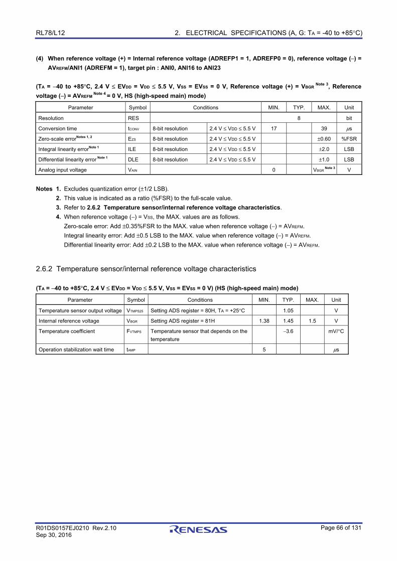
RL78/L12 2. ELECTRICAL SPECIFICATIONS (A, G: TA = -40 to +85°C)
R01DS0157EJ0210 Rev.2.10 Sep 30, 2016
Page 66 of 131
(4) When reference voltage (+) = Internal reference voltage (ADREFP1 = 1, ADREFP0 = 0), reference voltage (−) = AVREFM/ANI1 (ADREFM = 1), target pin : ANI0, ANI16 to ANI23
(TA = −40 to +85°C, 2.4 V ≤ EVDD = VDD ≤ 5.5 V, VSS = EVSS = 0 V, Reference voltage (+) = VBGR
Note 3, Reference voltage (−) = AVREFM
Note 4 = 0 V, HS (high-speed main) mode)
Parameter Symbol Conditions MIN. TYP. MAX. Unit
Resolution RES 8 bit
Conversion time tCONV 8-bit resolution 2.4 V ≤ VDD ≤ 5.5 V 17 39 μs
Zero-scale errorNotes 1, 2 EZS 8-bit resolution 2.4 V ≤ VDD ≤ 5.5 V ±0.60 %FSR
Integral linearity errorNote 1 ILE 8-bit resolution 2.4 V ≤ VDD ≤ 5.5 V ±2.0 LSB
Differential linearity error Note 1 DLE 8-bit resolution 2.4 V ≤ VDD ≤ 5.5 V ±1.0 LSB
Analog input voltage VAIN 0 VBGR Note 3 V
Notes 1. Excludes quantization error (±1/2 LSB).
2. This value is indicated as a ratio (%FSR) to the full-scale value.
3. Refer to 2.6.2 Temperature sensor/internal reference voltage characteristics.
4. When reference voltage (−) = VSS, the MAX. values are as follows.
Zero-scale error: Add ±0.35%FSR to the MAX. value when reference voltage (−) = AVREFM.
Integral linearity error: Add ±0.5 LSB to the MAX. value when reference voltage (−) = AVREFM.
Differential linearity error: Add ±0.2 LSB to the MAX. value when reference voltage (−) = AVREFM.
2.6.2 Temperature sensor/internal reference voltage characteristics
(TA = −40 to +85°C, 2.4 V ≤ EVDD = VDD ≤ 5.5 V, VSS = EVSS = 0 V) (HS (high-speed main) mode)
Parameter Symbol Conditions MIN. TYP. MAX. Unit
Temperature sensor output voltage VTMPS25 Setting ADS register = 80H, TA = +25°C 1.05 V
Internal reference voltage VBGR Setting ADS register = 81H 1.38 1.45 1.5 V
Temperature coefficient FVTMPS Temperature sensor that depends on the
temperature
−3.6 mV/°C
Operation stabilization wait time tAMP 5 μs
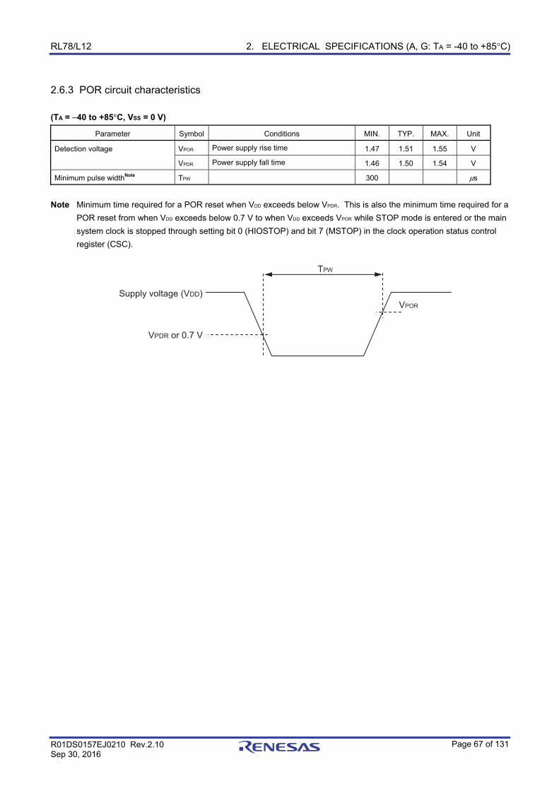
RL78/L12 2. ELECTRICAL SPECIFICATIONS (A, G: TA = -40 to +85°C)
R01DS0157EJ0210 Rev.2.10 Sep 30, 2016
Page 67 of 131
2.6.3 POR circuit characteristics
(TA = −40 to +85°C, VSS = 0 V)
Parameter Symbol Conditions MIN. TYP. MAX. Unit
Detection voltage VPOR Power supply rise time 1.47 1.51 1.55 V
VPDR Power supply fall time 1.46 1.50 1.54 V
Minimum pulse widthNote TPW 300 μs
Note Minimum time required for a POR reset when VDD exceeds below VPDR. This is also the minimum time required for a
POR reset from when VDD exceeds below 0.7 V to when VDD exceeds VPOR while STOP mode is entered or the main
system clock is stopped through setting bit 0 (HIOSTOP) and bit 7 (MSTOP) in the clock operation status control
register (CSC).
TPW
VPOR
VPDR or 0.7 V
Supply voltage (VDD)
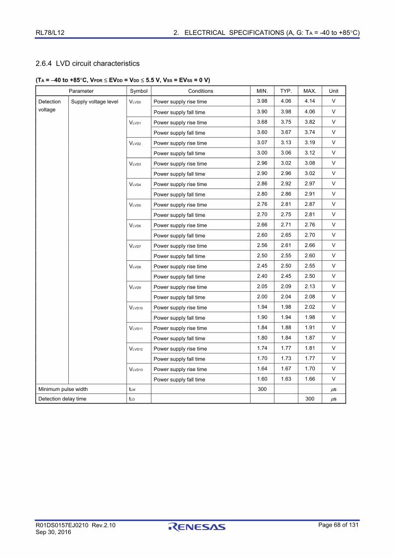
RL78/L12 2. ELECTRICAL SPECIFICATIONS (A, G: TA = -40 to +85°C)
R01DS0157EJ0210 Rev.2.10 Sep 30, 2016
Page 68 of 131
2.6.4 LVD circuit characteristics (TA = −40 to +85°C, VPDR ≤ EVDD = VDD ≤ 5.5 V, VSS = EVSS = 0 V)
Parameter Symbol Conditions MIN. TYP. MAX. Unit
Detection
voltage
Supply voltage level VLVD0 Power supply rise time 3.98 4.06 4.14 V
Power supply fall time 3.90 3.98 4.06 V
VLVD1 Power supply rise time 3.68 3.75 3.82 V
Power supply fall time 3.60 3.67 3.74 V
VLVD2 Power supply rise time 3.07 3.13 3.19 V
Power supply fall time 3.00 3.06 3.12 V
VLVD3 Power supply rise time 2.96 3.02 3.08 V
Power supply fall time 2.90 2.96 3.02 V
VLVD4 Power supply rise time 2.86 2.92 2.97 V
Power supply fall time 2.80 2.86 2.91 V
VLVD5 Power supply rise time 2.76 2.81 2.87 V
Power supply fall time 2.70 2.75 2.81 V
VLVD6 Power supply rise time 2.66 2.71 2.76 V
Power supply fall time 2.60 2.65 2.70 V
VLVD7 Power supply rise time 2.56 2.61 2.66 V
Power supply fall time 2.50 2.55 2.60 V
VLVD8 Power supply rise time 2.45 2.50 2.55 V
Power supply fall time 2.40 2.45 2.50 V
VLVD9 Power supply rise time 2.05 2.09 2.13 V
Power supply fall time 2.00 2.04 2.08 V
VLVD10 Power supply rise time 1.94 1.98 2.02 V
Power supply fall time 1.90 1.94 1.98 V
VLVD11 Power supply rise time 1.84 1.88 1.91 V
Power supply fall time 1.80 1.84 1.87 V
VLVD12 Power supply rise time 1.74 1.77 1.81 V
Power supply fall time 1.70 1.73 1.77 V
VLVD13 Power supply rise time 1.64 1.67 1.70 V
Power supply fall time 1.60 1.63 1.66 V
Minimum pulse width tLW 300 μs
Detection delay time tLD 300 μs
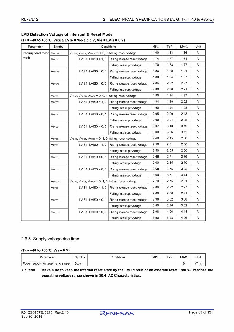
RL78/L12 2. ELECTRICAL SPECIFICATIONS (A, G: TA = -40 to +85°C)
R01DS0157EJ0210 Rev.2.10 Sep 30, 2016
Page 69 of 131
LVD Detection Voltage of Interrupt & Reset Mode (TA = −40 to +85°C, VPDR ≤ EVDD = VDD ≤ 5.5 V, VSS = EVSS = 0 V)
Parameter Symbol Conditions MIN. TYP. MAX. Unit
Interrupt and reset
mode
VLVDA0 VPOC2, VPOC1, VPOC0 = 0, 0, 0, falling reset voltage 1.60 1.63 1.66 V
VLVDA1 LVIS1, LVIS0 = 1, 0 Rising release reset voltage 1.74 1.77 1.81 V
Falling interrupt voltage 1.70 1.73 1.77 V
VLVDA2 LVIS1, LVIS0 = 0, 1 Rising release reset voltage 1.84 1.88 1.91 V
Falling interrupt voltage 1.80 1.84 1.87 V
VLVDA3 LVIS1, LVIS0 = 0, 0 Rising release reset voltage 2.86 2.92 2.97 V
Falling interrupt voltage 2.80 2.86 2.91 V
VLVDB1 VPOC2, VPOC1, VPOC0 = 0, 0, 1, falling reset voltage 1.80 1.84 1.87 V
VLVDB2 LVIS1, LVIS0 = 1, 0 Rising release reset voltage 1.94 1.98 2.02 V
Falling interrupt voltage 1.90 1.94 1.98 V
VLVDB3 LVIS1, LVIS0 = 0, 1 Rising release reset voltage 2.05 2.09 2.13 V
Falling interrupt voltage 2.00 2.04 2.08 V
VLVDB4 LVIS1, LVIS0 = 0, 0 Rising release reset voltage 3.07 3.13 3.19 V
Falling interrupt voltage 3.00 3.06 3.12 V
VLVDC0 VPOC2, VPOC1, VPOC0 = 0, 1, 0, falling reset voltage 2.40 2.45 2.50 V
VLVDC1 LVIS1, LVIS0 = 1, 0 Rising release reset voltage 2.56 2.61 2.66 V
Falling interrupt voltage 2.50 2.55 2.60 V
VLVDC2 LVIS1, LVIS0 = 0, 1 Rising release reset voltage 2.66 2.71 2.76 V
Falling interrupt voltage 2.60 2.65 2.70 V
VLVDC3 LVIS1, LVIS0 = 0, 0 Rising release reset voltage 3.68 3.75 3.82 V
Falling interrupt voltage 3.60 3.67 3.74 V
VLVDD0 VPOC2, VPOC1, VPOC0 = 0, 1, 1, falling reset voltage 2.70 2.75 2.81 V
VLVDD1 LVIS1, LVIS0 = 1, 0 Rising release reset voltage 2.86 2.92 2.97 V
Falling interrupt voltage 2.80 2.86 2.91 V
VLVDD2 LVIS1, LVIS0 = 0, 1 Rising release reset voltage 2.96 3.02 3.08 V
Falling interrupt voltage 2.90 2.96 3.02 V
VLVDD3 LVIS1, LVIS0 = 0, 0 Rising release reset voltage 3.98 4.06 4.14 V
Falling interrupt voltage 3.90 3.98 4.06 V
2.6.5 Supply voltage rise time (TA = −40 to +85°C, VSS = 0 V)
Parameter Symbol Conditions MIN. TYP. MAX. Unit
Power supply voltage rising slope SVDD 54 V/ms
Caution Make sure to keep the internal reset state by the LVD circuit or an external reset until VDD reaches the operating voltage range shown in 30.4 AC Characteristics.
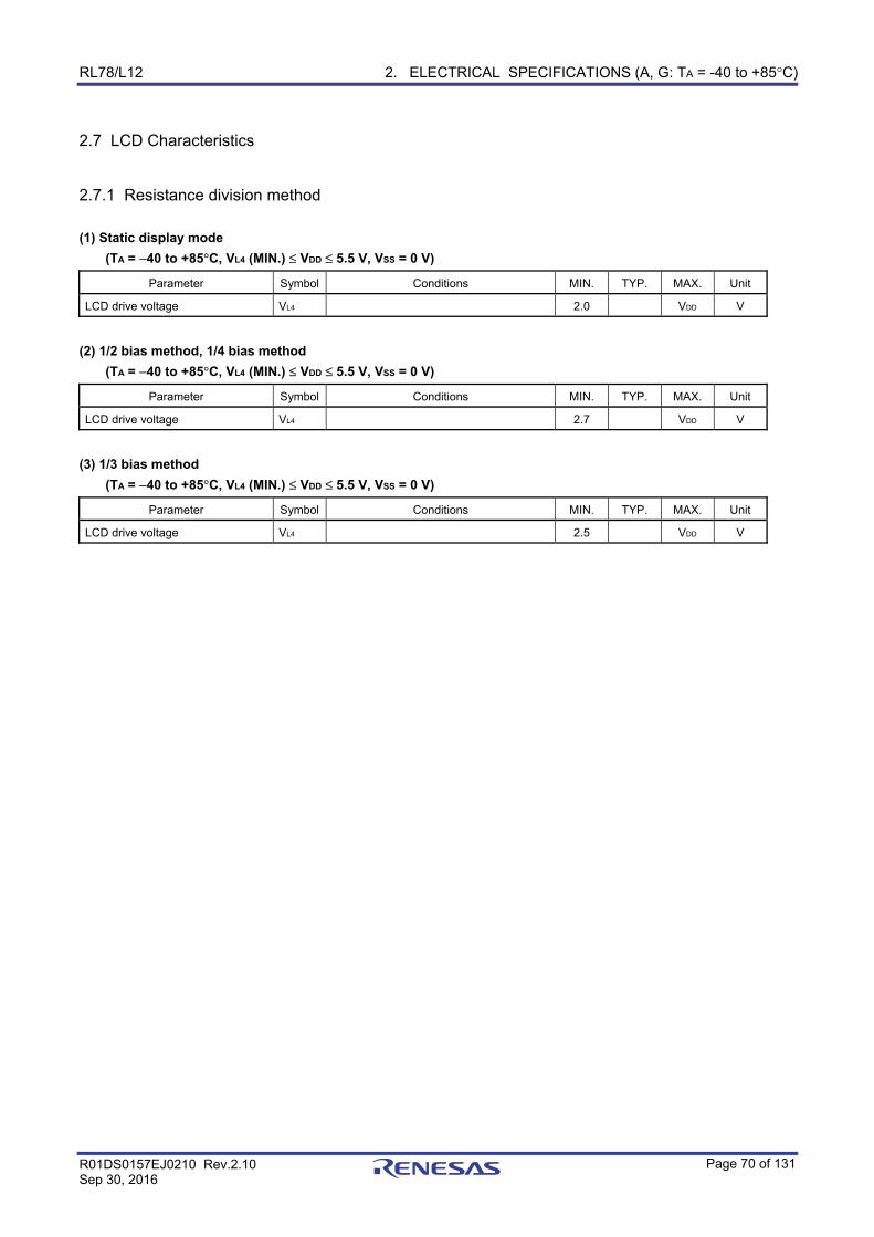
RL78/L12 2. ELECTRICAL SPECIFICATIONS (A, G: TA = -40 to +85°C)
R01DS0157EJ0210 Rev.2.10 Sep 30, 2016
Page 70 of 131
2.7 LCD Characteristics
2.7.1 Resistance division method (1) Static display mode
(TA = −40 to +85°C, VL4 (MIN.) ≤ VDD ≤ 5.5 V, VSS = 0 V)
Parameter Symbol Conditions MIN. TYP. MAX. Unit
LCD drive voltage VL4 2.0 VDD V
(2) 1/2 bias method, 1/4 bias method (TA = −40 to +85°C, VL4 (MIN.) ≤ VDD ≤ 5.5 V, VSS = 0 V)
Parameter Symbol Conditions MIN. TYP. MAX. Unit
LCD drive voltage VL4 2.7 VDD V
(3) 1/3 bias method
(TA = −40 to +85°C, VL4 (MIN.) ≤ VDD ≤ 5.5 V, VSS = 0 V)
Parameter Symbol Conditions MIN. TYP. MAX. Unit
LCD drive voltage VL4 2.5 VDD V
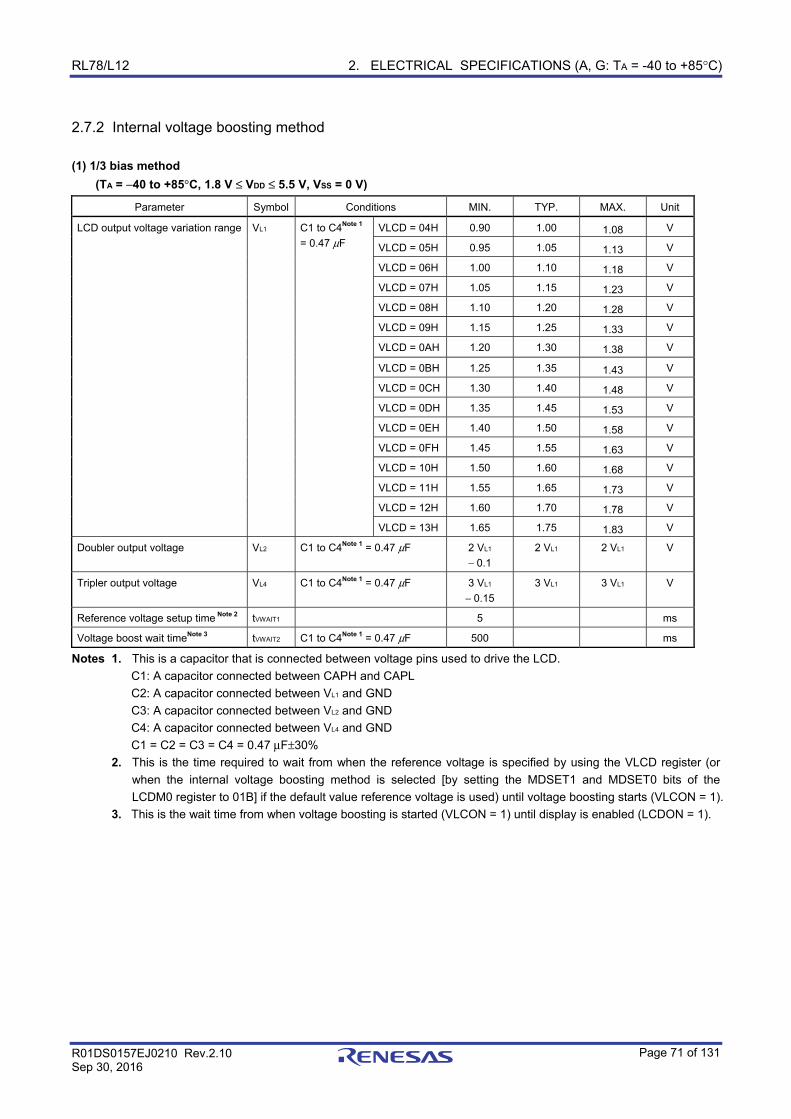
RL78/L12 2. ELECTRICAL SPECIFICATIONS (A, G: TA = -40 to +85°C)
R01DS0157EJ0210 Rev.2.10 Sep 30, 2016
Page 71 of 131
2.7.2 Internal voltage boosting method (1) 1/3 bias method
(TA = −40 to +85°C, 1.8 V ≤ VDD ≤ 5.5 V, VSS = 0 V)
Parameter Symbol Conditions MIN. TYP. MAX. Unit
LCD output voltage variation range VL1 C1 to C4Note 1
= 0.47 μF
VLCD = 04H 0.90 1.00 1.08 V
VLCD = 05H 0.95 1.05 1.13 V
VLCD = 06H 1.00 1.10 1.18 V
VLCD = 07H 1.05 1.15 1.23 V
VLCD = 08H 1.10 1.20 1.28 V
VLCD = 09H 1.15 1.25 1.33 V
VLCD = 0AH 1.20 1.30 1.38 V
VLCD = 0BH 1.25 1.35 1.43 V
VLCD = 0CH 1.30 1.40 1.48 V
VLCD = 0DH 1.35 1.45 1.53 V
VLCD = 0EH 1.40 1.50 1.58 V
VLCD = 0FH 1.45 1.55 1.63 V
VLCD = 10H 1.50 1.60 1.68 V
VLCD = 11H 1.55 1.65 1.73 V
VLCD = 12H 1.60 1.70 1.78 V
VLCD = 13H 1.65 1.75 1.83 V
Doubler output voltage VL2 C1 to C4Note 1 = 0.47 μF 2 VL1
− 0.1
2 VL1 2 VL1 V
Tripler output voltage VL4 C1 to C4Note 1 = 0.47 μF 3 VL1
− 0.15
3 VL1 3 VL1 V
Reference voltage setup time Note 2 tVWAIT1 5 ms
Voltage boost wait timeNote 3 tVWAIT2 C1 to C4Note 1 = 0.47 μF 500 ms
Notes 1. This is a capacitor that is connected between voltage pins used to drive the LCD.
C1: A capacitor connected between CAPH and CAPL
C2: A capacitor connected between VL1 and GND
C3: A capacitor connected between VL2 and GND
C4: A capacitor connected between VL4 and GND
C1 = C2 = C3 = C4 = 0.47 μF±30%
2. This is the time required to wait from when the reference voltage is specified by using the VLCD register (or
when the internal voltage boosting method is selected [by setting the MDSET1 and MDSET0 bits of the
LCDM0 register to 01B] if the default value reference voltage is used) until voltage boosting starts (VLCON = 1).
3. This is the wait time from when voltage boosting is started (VLCON = 1) until display is enabled (LCDON = 1).
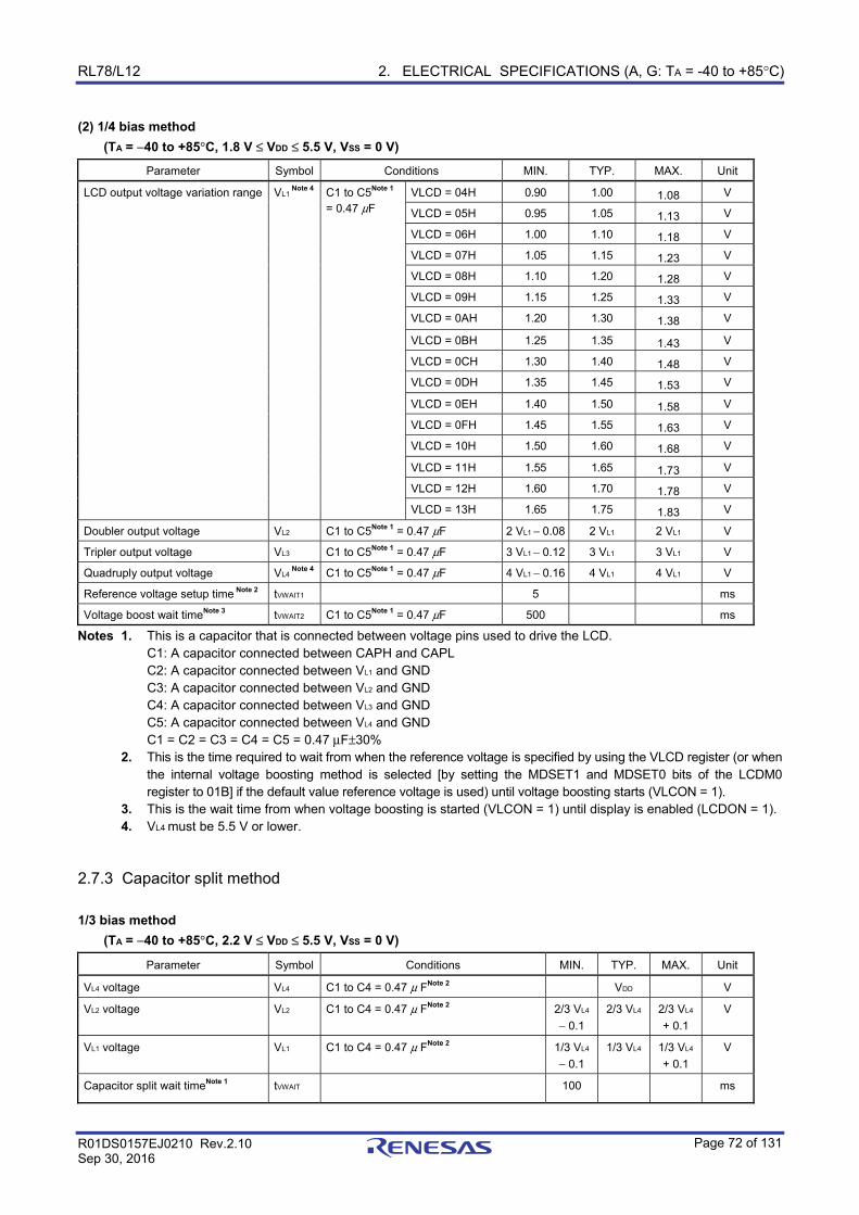
RL78/L12 2. ELECTRICAL SPECIFICATIONS (A, G: TA = -40 to +85°C)
R01DS0157EJ0210 Rev.2.10 Sep 30, 2016
Page 72 of 131
(2) 1/4 bias method (TA = −40 to +85°C, 1.8 V ≤ VDD ≤ 5.5 V, VSS = 0 V)
Parameter Symbol Conditions MIN. TYP. MAX. Unit
LCD output voltage variation range VL1 Note 4 C1 to C5Note 1
= 0.47 μF VLCD = 04H 0.90 1.00 1.08 V
VLCD = 05H 0.95 1.05 1.13 V
VLCD = 06H 1.00 1.10 1.18 V
VLCD = 07H 1.05 1.15 1.23 V
VLCD = 08H 1.10 1.20 1.28 V
VLCD = 09H 1.15 1.25 1.33 V
VLCD = 0AH 1.20 1.30 1.38 V
VLCD = 0BH 1.25 1.35 1.43 V
VLCD = 0CH 1.30 1.40 1.48 V
VLCD = 0DH 1.35 1.45 1.53 V
VLCD = 0EH 1.40 1.50 1.58 V
VLCD = 0FH 1.45 1.55 1.63 V
VLCD = 10H 1.50 1.60 1.68 V
VLCD = 11H 1.55 1.65 1.73 V
VLCD = 12H 1.60 1.70 1.78 V
VLCD = 13H 1.65 1.75 1.83 V
Doubler output voltage VL2 C1 to C5Note 1 = 0.47 μF 2 VL1 − 0.08 2 VL1 2 VL1 V
Tripler output voltage VL3 C1 to C5Note 1 = 0.47 μF 3 VL1 − 0.12 3 VL1 3 VL1 V
Quadruply output voltage VL4 Note 4 C1 to C5Note 1 = 0.47 μF 4 VL1 − 0.16 4 VL1 4 VL1 V
Reference voltage setup time Note 2 tVWAIT1 5 ms
Voltage boost wait timeNote 3 tVWAIT2 C1 to C5Note 1 = 0.47 μF 500 ms
Notes 1. This is a capacitor that is connected between voltage pins used to drive the LCD. C1: A capacitor connected between CAPH and CAPL C2: A capacitor connected between VL1 and GND C3: A capacitor connected between VL2 and GND C4: A capacitor connected between VL3 and GND C5: A capacitor connected between VL4 and GND C1 = C2 = C3 = C4 = C5 = 0.47 μF±30% 2. This is the time required to wait from when the reference voltage is specified by using the VLCD register (or when
the internal voltage boosting method is selected [by setting the MDSET1 and MDSET0 bits of the LCDM0 register to 01B] if the default value reference voltage is used) until voltage boosting starts (VLCON = 1).
3. This is the wait time from when voltage boosting is started (VLCON = 1) until display is enabled (LCDON = 1). 4. VL4 must be 5.5 V or lower.
2.7.3 Capacitor split method 1/3 bias method
(TA = −40 to +85°C, 2.2 V ≤ VDD ≤ 5.5 V, VSS = 0 V)
Parameter Symbol Conditions MIN. TYP. MAX. Unit
VL4 voltage VL4 C1 to C4 = 0.47 μ FNote 2 VDD V
VL2 voltage VL2 C1 to C4 = 0.47 μ FNote 2 2/3 VL4
− 0.1
2/3 VL4 2/3 VL4
+ 0.1
V
VL1 voltage VL1 C1 to C4 = 0.47 μ FNote 2 1/3 VL4
− 0.1
1/3 VL4 1/3 VL4
+ 0.1
V
Capacitor split wait timeNote 1 tVWAIT 100 ms
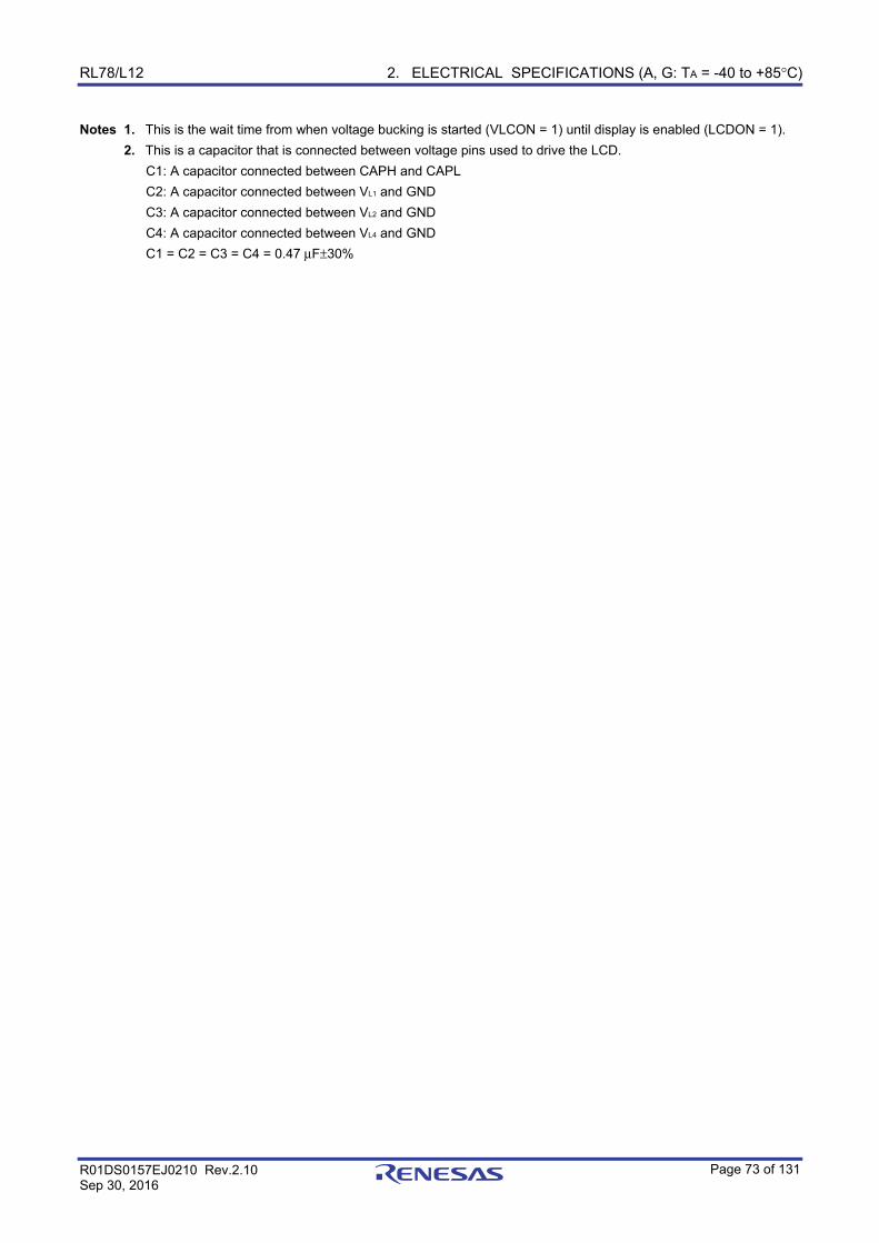
RL78/L12 2. ELECTRICAL SPECIFICATIONS (A, G: TA = -40 to +85°C)
R01DS0157EJ0210 Rev.2.10 Sep 30, 2016
Page 73 of 131
Notes 1. This is the wait time from when voltage bucking is started (VLCON = 1) until display is enabled (LCDON = 1).
2. This is a capacitor that is connected between voltage pins used to drive the LCD.
C1: A capacitor connected between CAPH and CAPL
C2: A capacitor connected between VL1 and GND
C3: A capacitor connected between VL2 and GND
C4: A capacitor connected between VL4 and GND
C1 = C2 = C3 = C4 = 0.47 μF±30%
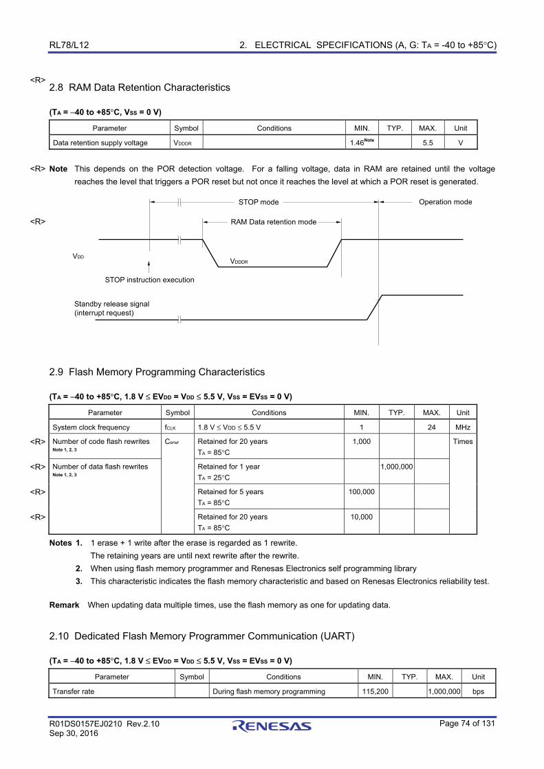
RL78/L12 2. ELECTRICAL SPECIFICATIONS (A, G: TA = -40 to +85°C)
R01DS0157EJ0210 Rev.2.10 Sep 30, 2016
Page 74 of 131
2.8 RAM Data Retention Characteristics (TA = −40 to +85°C, VSS = 0 V)
Parameter Symbol Conditions MIN. TYP. MAX. Unit
Data retention supply voltage VDDDR 1.46Note 5.5 V
Note This depends on the POR detection voltage. For a falling voltage, data in RAM are retained until the voltage
reaches the level that triggers a POR reset but not once it reaches the level at which a POR reset is generated.
VDD
STOP instruction execution
Standby release signal(interrupt request)
STOP mode
RAM Data retention mode
VDDDR
Operation mode
2.9 Flash Memory Programming Characteristics (TA = −40 to +85°C, 1.8 V ≤ EVDD = VDD ≤ 5.5 V, VSS = EVSS = 0 V)
Parameter Symbol Conditions MIN. TYP. MAX. Unit
System clock frequency fCLK 1.8 V ≤ VDD ≤ 5.5 V 1 24 MHz
Number of code flash rewrites Note 1, 2, 3
Cerwr Retained for 20 years
TA = 85°C
1,000 Times
Number of data flash rewrites Note 1, 2, 3
Retained for 1 year
TA = 25°C
1,000,000
Retained for 5 years
TA = 85°C
100,000
Retained for 20 years
TA = 85°C
10,000
Notes 1. 1 erase + 1 write after the erase is regarded as 1 rewrite.
The retaining years are until next rewrite after the rewrite.
2. When using flash memory programmer and Renesas Electronics self programming library
3. This characteristic indicates the flash memory characteristic and based on Renesas Electronics reliability test. Remark When updating data multiple times, use the flash memory as one for updating data.
2.10 Dedicated Flash Memory Programmer Communication (UART) (TA = −40 to +85°C, 1.8 V ≤ EVDD = VDD ≤ 5.5 V, VSS = EVSS = 0 V)
Parameter Symbol Conditions MIN. TYP. MAX. Unit
Transfer rate During flash memory programming 115,200 1,000,000 bps
<R>
<R>
<R>
<R>
<R>
<R>
<R>
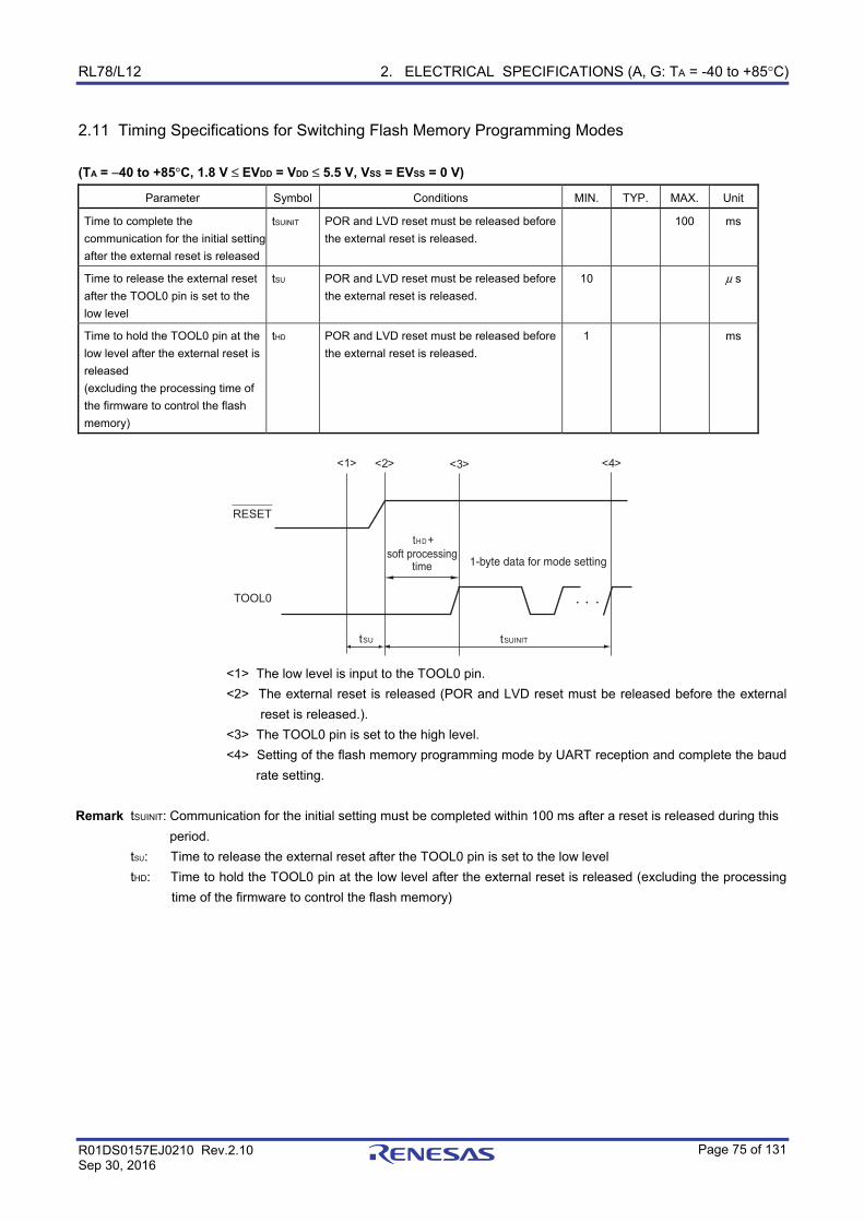
RL78/L12 2. ELECTRICAL SPECIFICATIONS (A, G: TA = -40 to +85°C)
R01DS0157EJ0210 Rev.2.10 Sep 30, 2016
Page 75 of 131
2.11 Timing Specifications for Switching Flash Memory Programming Modes (TA = −40 to +85°C, 1.8 V ≤ EVDD = VDD ≤ 5.5 V, VSS = EVSS = 0 V)
Parameter Symbol Conditions MIN. TYP. MAX. Unit
Time to complete the
communication for the initial setting
after the external reset is released
tSUINIT POR and LVD reset must be released before
the external reset is released.
100 ms
Time to release the external reset
after the TOOL0 pin is set to the
low level
tSU POR and LVD reset must be released before
the external reset is released.
10 μ s
Time to hold the TOOL0 pin at the
low level after the external reset is
released
(excluding the processing time of
the firmware to control the flash
memory)
tHD POR and LVD reset must be released before
the external reset is released.
1 ms
RESET
TOOL0
<1> <2> <3>
tSUINIT
tH D+
soft processingtime
tSU
<4>
1-byte data for mode setting
<1> The low level is input to the TOOL0 pin.
<2> The external reset is released (POR and LVD reset must be released before the external
reset is released.).
<3> The TOOL0 pin is set to the high level.
<4> Setting of the flash memory programming mode by UART reception and complete the baud
rate setting.
Remark tSUINIT: Communication for the initial setting must be completed within 100 ms after a reset is released during this
period.
tSU: Time to release the external reset after the TOOL0 pin is set to the low level
tHD: Time to hold the TOOL0 pin at the low level after the external reset is released (excluding the processing
time of the firmware to control the flash memory)
RL78/L12 3. ELECTRICAL SPECIFICATIONS (G: TA = -40 to +105°C)
R01DS0157EJ0210 Rev.2.10 Sep 30, 2016
Page 76 of 131
3. ELECTRICAL SPECIFICATIONS (G: TA = -40 to +105°C)
This chapter describes the electrical specifications for the products "G: Industrial applications (TA = -40 to +105°C)". Cautions 1. The RL78 microcontrollers have an on-chip debug function, which is provided for development
and evaluation. Do not use the on-chip debug function in products designated for mass production, because the guaranteed number of rewritable times of the flash memory may be exceeded when this function is used, and product reliability therefore cannot be guaranteed. Renesas Electronics is not liable for problems occurring when the on-chip debug function is used.
2. With products not provided with an EVDD or EVSS pin, replace EVDD with VDD, or replace EVSS with VSS.
3. For derating with TA = +85 to +105°C, contact our Sales Division or the vender's sales division. Derating means the specified reduction in an operating parameter to improve reliability.
RL78/L12 3. ELECTRICAL SPECIFICATIONS (G: TA = -40 to +105°C)
R01DS0157EJ0210 Rev.2.10 Sep 30, 2016
Page 77 of 131
There are following differences between the products "G: Industrial applications (TA = -40 to +105°C)" and the products “A:
Consumer applications, and G: Industrial applications (TA = -40 to +85°C)”.
Parameter Application
A: Consumer applications,
G: Industrial applications
(with TA = -40 to +85°C)
G: Industrial applications
Operating ambient temperature TA = -40 to +85°C TA = -40 to +105°C
Operating mode
Operating voltage range
HS (high-speed main) mode:
2.7 V ≤ VDD ≤ 5.5 V@1 MHz to 32 MHz
2.4 V ≤ VDD ≤ 5.5 V@1 MHz to 16 MHz
LS (low-speed main) mode:
1.8 V ≤ VDD ≤ 5.5 V@1 MHz to 8 MHz
LV (low-voltage main) mode:
1.6 V ≤ VDD ≤ 5.5 V@1 MHz to 4 MHz
HS (high-speed main) mode only:
2.7 V ≤ VDD ≤ 5.5 V@1 MHz to 32 MHz
2.4 V ≤ VDD ≤ 5.5 V@1 MHz to 16 MHz
High-speed on-chip oscillator clock
accuracy
1.8 V ≤ VDD ≤ 5.5 V:
±1.0%@ TA = -20 to +85°C
±1.5%@ TA = -40 to -20°C
1.6 V ≤ VDD < 1.8 V:
±5.0%@ TA = -20 to +85°C
±5.5%@ TA = -40 to -20°C
2.4 V ≤ VDD ≤ 5.5 V:
±2.0%@ TA = +85 to +105°C
±1.0%@ TA = -20 to +85°C
±1.5%@ TA = -40 to -20°C
Serial array unit UART
CSI00: fCLK/2 (supporting 16 Mbps), fCLK/4
CSI01
Simplified I2C communication
UART
CSI00: fCLK/4
CSI01
Simplified I2C communication
IICA Normal mode
Fast mode
Fast mode plus
Normal mode
Fast mode
Voltage detector Rise detection voltage: 1.67 V to 4.06 V
(14 levels)
Fall detection voltage: 1.63 V to 3.98 V
(14 levels)
Rise detection voltage: 2.61 V to 4.06 V
(8 levels)
Fall detection voltage: 2.55 V to 3.98 V
(8 levels)
Remark The electrical characteristics of the products G: Industrial applications (TA = -40 to +105°C) are different from
those of the products “A: Consumer applications, and G: Industrial applications (only with TA = -40 to +85°C)”.
For details, refer to 3.1 to 3.10.
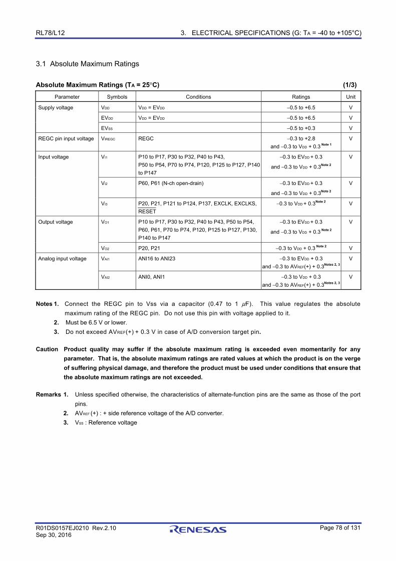
RL78/L12 3. ELECTRICAL SPECIFICATIONS (G: TA = -40 to +105°C)
R01DS0157EJ0210 Rev.2.10 Sep 30, 2016
Page 78 of 131
3.1 Absolute Maximum Ratings Absolute Maximum Ratings (TA = 25°C) (1/3)
Parameter Symbols Conditions Ratings Unit
Supply voltage VDD VDD = EVDD −0.5 to +6.5 V
EVDD VDD = EVDD −0.5 to +6.5 V
EVSS −0.5 to +0.3 V
REGC pin input voltage VIREGC REGC −0.3 to +2.8
and −0.3 to VDD + 0.3 Note 1
V
Input voltage VI1 P10 to P17, P30 to P32, P40 to P43,
P50 to P54, P70 to P74, P120, P125 to P127, P140
to P147
−0.3 to EVDD + 0.3
and −0.3 to VDD + 0.3Note 2
V
VI2 P60, P61 (N-ch open-drain) −0.3 to EVDD + 0.3
and −0.3 to VDD + 0.3Note 2
V
VI3 P20, P21, P121 to P124, P137, EXCLK, EXCLKS,
RESET
−0.3 to VDD + 0.3Note 2 V
Output voltage VO1 P10 to P17, P30 to P32, P40 to P43, P50 to P54,
P60, P61, P70 to P74, P120, P125 to P127, P130,
P140 to P147
−0.3 to EVDD + 0.3
and −0.3 to VDD + 0.3 Note 2
V
VO2 P20, P21 −0.3 to VDD + 0.3 Note 2 V
Analog input voltage VAI1 ANI16 to ANI23 −0.3 to EVDD + 0.3
and −0.3 to AVREF(+) + 0.3Notes 2, 3V
VAI2 ANI0, ANI1 −0.3 to VDD + 0.3
and −0.3 to AVREF(+) + 0.3Notes 2, 3V
Notes 1. Connect the REGC pin to Vss via a capacitor (0.47 to 1 μF). This value regulates the absolute
maximum rating of the REGC pin. Do not use this pin with voltage applied to it.
2. Must be 6.5 V or lower.
3. Do not exceed AVREF(+) + 0.3 V in case of A/D conversion target pin.
Caution Product quality may suffer if the absolute maximum rating is exceeded even momentarily for any parameter. That is, the absolute maximum ratings are rated values at which the product is on the verge of suffering physical damage, and therefore the product must be used under conditions that ensure that the absolute maximum ratings are not exceeded.
Remarks 1. Unless specified otherwise, the characteristics of alternate-function pins are the same as those of the port
pins.
2. AVREF (+) : + side reference voltage of the A/D converter.
3. VSS : Reference voltage
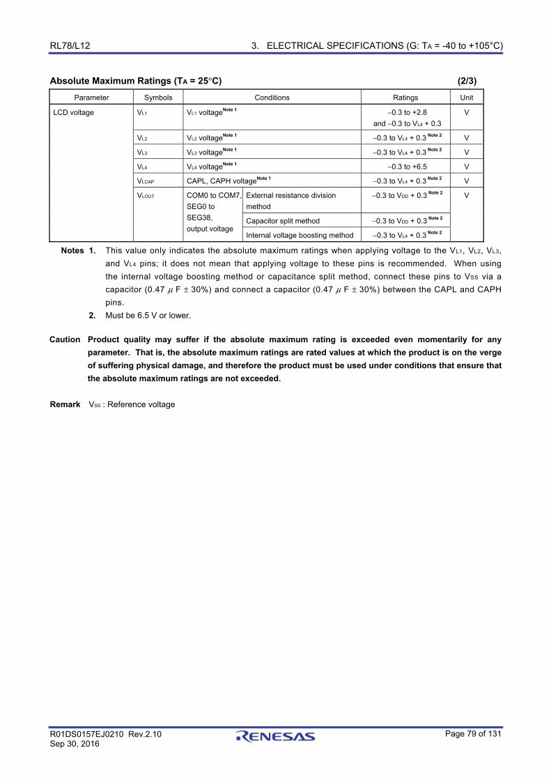
RL78/L12 3. ELECTRICAL SPECIFICATIONS (G: TA = -40 to +105°C)
R01DS0157EJ0210 Rev.2.10 Sep 30, 2016
Page 79 of 131
Absolute Maximum Ratings (TA = 25°C) (2/3) Parameter Symbols Conditions Ratings Unit
LCD voltage VL1 VL1 voltageNote 1 −0.3 to +2.8
and −0.3 to VL4 + 0.3
V
VL2 VL2 voltageNote 1 −0.3 to VL4 + 0.3 Note 2 V
VL3 VL3 voltageNote 1 −0.3 to VL4 + 0.3 Note 2 V
VL4 VL4 voltageNote 1 −0.3 to +6.5 V
VLCAP CAPL, CAPH voltageNote 1 −0.3 to VL4 + 0.3 Note 2 V
VLOUT COM0 to COM7,
SEG0 to
SEG38,
output voltage
External resistance division
method
−0.3 to VDD + 0.3 Note 2 V
Capacitor split method −0.3 to VDD + 0.3 Note 2
Internal voltage boosting method −0.3 to VL4 + 0.3 Note 2
Notes 1. This value only indicates the absolute maximum ratings when applying voltage to the VL1, VL2, VL3,
and VL4 pins; it does not mean that applying voltage to these pins is recommended. When using
the internal voltage boosting method or capacitance split method, connect these pins to VSS via a
capacitor (0.47 μ F ± 30%) and connect a capacitor (0.47 μ F ± 30%) between the CAPL and CAPH
pins.
2. Must be 6.5 V or lower.
Caution Product quality may suffer if the absolute maximum rating is exceeded even momentarily for any parameter. That is, the absolute maximum ratings are rated values at which the product is on the verge of suffering physical damage, and therefore the product must be used under conditions that ensure that the absolute maximum ratings are not exceeded.
Remark VSS : Reference voltage
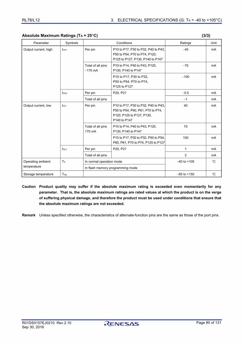
RL78/L12 3. ELECTRICAL SPECIFICATIONS (G: TA = -40 to +105°C)
R01DS0157EJ0210 Rev.2.10 Sep 30, 2016
Page 80 of 131
Absolute Maximum Ratings (TA = 25°C) (3/3) Parameter Symbols Conditions Ratings Unit
Output current, high IOH1 Per pin P10 to P17, P30 to P32, P40 to P43,
P50 to P54, P70 to P74, P120,
P125 to P127, P130, P140 to P147
−40 mA
Total of all pins
−170 mA
P10 to P14, P40 to P43, P120,
P130, P140 to P147
−70 mA
P15 to P17, P30 to P32,
P50 to P54, P70 to P74,
P125 to P127
−100 mA
IOH2 Per pin P20, P21 −0.5 mA
Total of all pins −1 mA
Output current, low IOL1 Per pin P10 to P17, P30 to P32, P40 to P43,
P50 to P54, P60, P61, P70 to P74,
P120, P125 to P127, P130,
P140 to P147
40 mA
Total of all pins
170 mA
P10 to P14, P40 to P43, P120,
P130, P140 to P147
70 mA
P15 to P17, P30 to P32, P50 to P54,
P60, P61, P70 to P74, P125 to P127
100 mA
IOL2 Per pin P20, P21 1 mA
Total of all pins 2 mA
Operating ambient
temperature
TA In normal operation mode −40 to +105 °C
In flash memory programming mode
Storage temperature Tstg −65 to +150 °C
Caution Product quality may suffer if the absolute maximum rating is exceeded even momentarily for any
parameter. That is, the absolute maximum ratings are rated values at which the product is on the verge of suffering physical damage, and therefore the product must be used under conditions that ensure that the absolute maximum ratings are not exceeded.
Remark Unless specified otherwise, the characteristics of alternate-function pins are the same as those of the port pins.
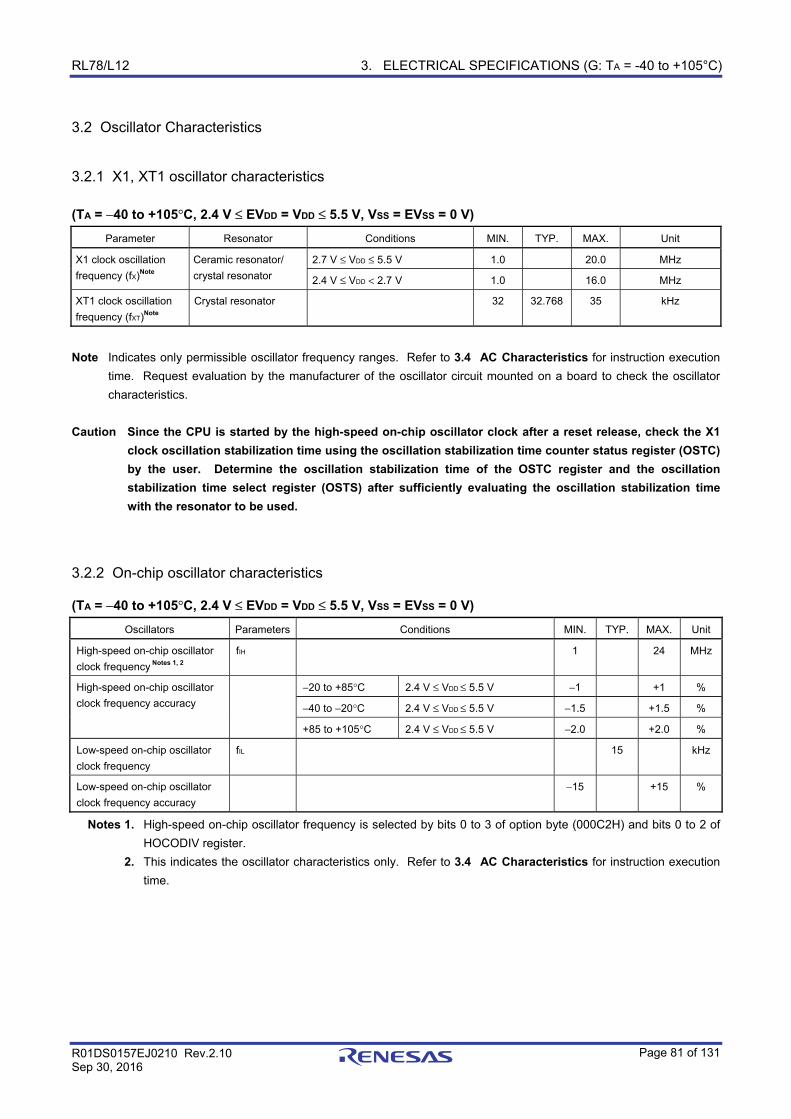
RL78/L12 3. ELECTRICAL SPECIFICATIONS (G: TA = -40 to +105°C)
R01DS0157EJ0210 Rev.2.10 Sep 30, 2016
Page 81 of 131
3.2 Oscillator Characteristics
3.2.1 X1, XT1 oscillator characteristics (TA = −40 to +105°C, 2.4 V ≤ EVDD = VDD ≤ 5.5 V, VSS = EVSS = 0 V)
Parameter Resonator Conditions MIN. TYP. MAX. Unit
X1 clock oscillation
frequency (fX)Note
Ceramic resonator/
crystal resonator
2.7 V ≤ VDD ≤ 5.5 V 1.0 20.0 MHz
2.4 V ≤ VDD < 2.7 V 1.0 16.0 MHz
XT1 clock oscillation
frequency (fXT)Note
Crystal resonator 32 32.768 35 kHz
Note Indicates only permissible oscillator frequency ranges. Refer to 3.4 AC Characteristics for instruction execution
time. Request evaluation by the manufacturer of the oscillator circuit mounted on a board to check the oscillator
characteristics.
Caution Since the CPU is started by the high-speed on-chip oscillator clock after a reset release, check the X1 clock oscillation stabilization time using the oscillation stabilization time counter status register (OSTC) by the user. Determine the oscillation stabilization time of the OSTC register and the oscillation stabilization time select register (OSTS) after sufficiently evaluating the oscillation stabilization time with the resonator to be used.
3.2.2 On-chip oscillator characteristics (TA = −40 to +105°C, 2.4 V ≤ EVDD = VDD ≤ 5.5 V, VSS = EVSS = 0 V)
Oscillators Parameters Conditions MIN. TYP. MAX. Unit
High-speed on-chip oscillator
clock frequency Notes 1, 2
fIH 1 24 MHz
High-speed on-chip oscillator
clock frequency accuracy
−20 to +85°C 2.4 V ≤ VDD ≤ 5.5 V −1 +1 %
−40 to −20°C 2.4 V ≤ VDD ≤ 5.5 V −1.5 +1.5 %
+85 to +105°C 2.4 V ≤ VDD ≤ 5.5 V −2.0 +2.0 %
Low-speed on-chip oscillator
clock frequency
fIL 15 kHz
Low-speed on-chip oscillator
clock frequency accuracy
−15 +15 %
Notes 1. High-speed on-chip oscillator frequency is selected by bits 0 to 3 of option byte (000C2H) and bits 0 to 2 of
HOCODIV register.
2. This indicates the oscillator characteristics only. Refer to 3.4 AC Characteristics for instruction execution
time.
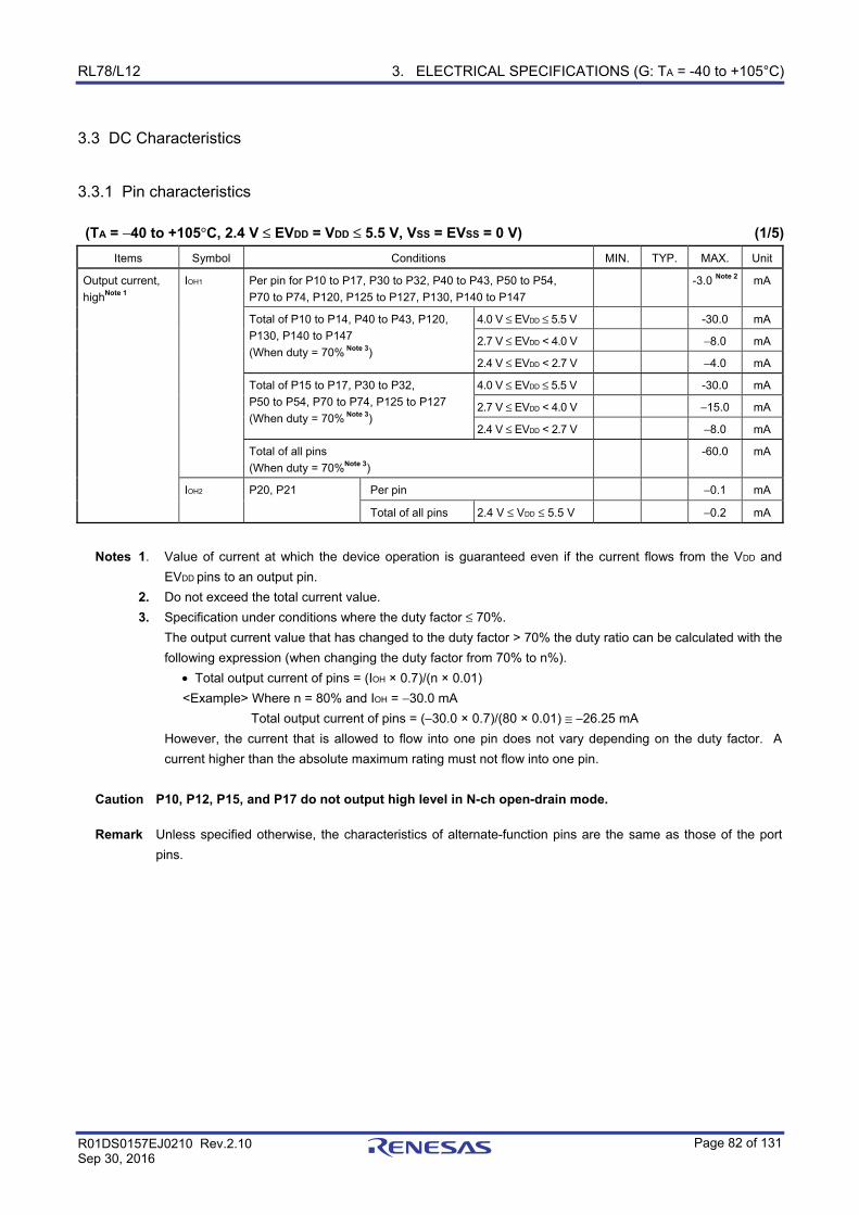
RL78/L12 3. ELECTRICAL SPECIFICATIONS (G: TA = -40 to +105°C)
R01DS0157EJ0210 Rev.2.10 Sep 30, 2016
Page 82 of 131
3.3 DC Characteristics
3.3.1 Pin characteristics (TA = −40 to +105°C, 2.4 V ≤ EVDD = VDD ≤ 5.5 V, VSS = EVSS = 0 V) (1/5)
Items Symbol Conditions MIN. TYP. MAX. Unit
Output current,
highNote 1
IOH1 Per pin for P10 to P17, P30 to P32, P40 to P43, P50 to P54,
P70 to P74, P120, P125 to P127, P130, P140 to P147
-3.0 Note 2 mA
Total of P10 to P14, P40 to P43, P120,
P130, P140 to P147
(When duty = 70% Note 3)
4.0 V ≤ EVDD ≤ 5.5 V -30.0 mA
2.7 V ≤ EVDD < 4.0 V −8.0 mA
2.4 V ≤ EVDD < 2.7 V −4.0 mA
Total of P15 to P17, P30 to P32,
P50 to P54, P70 to P74, P125 to P127
(When duty = 70% Note 3)
4.0 V ≤ EVDD ≤ 5.5 V -30.0 mA
2.7 V ≤ EVDD < 4.0 V −15.0 mA
2.4 V ≤ EVDD < 2.7 V −8.0 mA
Total of all pins
(When duty = 70%Note 3)
-60.0 mA
IOH2 P20, P21 Per pin −0.1 mA
Total of all pins 2.4 V ≤ VDD ≤ 5.5 V −0.2 mA
Notes 1. Value of current at which the device operation is guaranteed even if the current flows from the VDD and
EVDD pins to an output pin.
2. Do not exceed the total current value.
3. Specification under conditions where the duty factor ≤ 70%.
The output current value that has changed to the duty factor > 70% the duty ratio can be calculated with the
following expression (when changing the duty factor from 70% to n%).
• Total output current of pins = (IOH × 0.7)/(n × 0.01)
<Example> Where n = 80% and IOH = −30.0 mA
Total output current of pins = (−30.0 × 0.7)/(80 × 0.01) ≅ −26.25 mA
However, the current that is allowed to flow into one pin does not vary depending on the duty factor. A
current higher than the absolute maximum rating must not flow into one pin.
Caution P10, P12, P15, and P17 do not output high level in N-ch open-drain mode.
Remark Unless specified otherwise, the characteristics of alternate-function pins are the same as those of the port
pins.
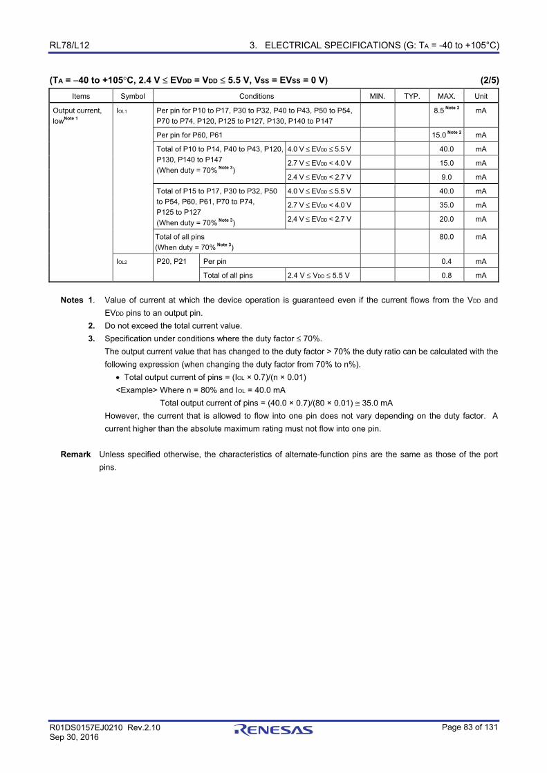
RL78/L12 3. ELECTRICAL SPECIFICATIONS (G: TA = -40 to +105°C)
R01DS0157EJ0210 Rev.2.10 Sep 30, 2016
Page 83 of 131
(TA = −40 to +105°C, 2.4 V ≤ EVDD = VDD ≤ 5.5 V, VSS = EVSS = 0 V) (2/5) Items Symbol Conditions MIN. TYP. MAX. Unit
Output current,
lowNote 1
IOL1 Per pin for P10 to P17, P30 to P32, P40 to P43, P50 to P54,
P70 to P74, P120, P125 to P127, P130, P140 to P147
8.5 Note 2 mA
Per pin for P60, P61 15.0 Note 2 mA
Total of P10 to P14, P40 to P43, P120,
P130, P140 to P147
(When duty = 70% Note 3)
4.0 V ≤ EVDD ≤ 5.5 V 40.0 mA
2.7 V ≤ EVDD < 4.0 V 15.0 mA
2.4 V ≤ EVDD < 2.7 V 9.0 mA
Total of P15 to P17, P30 to P32, P50
to P54, P60, P61, P70 to P74,
P125 to P127
(When duty = 70% Note 3)
4.0 V ≤ EVDD ≤ 5.5 V 40.0 mA
2.7 V ≤ EVDD < 4.0 V 35.0 mA
2,4 V ≤ EVDD < 2.7 V 20.0 mA
Total of all pins
(When duty = 70% Note 3)
80.0 mA
IOL2 P20, P21 Per pin 0.4 mA
Total of all pins 2.4 V ≤ VDD ≤ 5.5 V 0.8 mA
Notes 1. Value of current at which the device operation is guaranteed even if the current flows from the VDD and
EVDD pins to an output pin.
2. Do not exceed the total current value.
3. Specification under conditions where the duty factor ≤ 70%.
The output current value that has changed to the duty factor > 70% the duty ratio can be calculated with the
following expression (when changing the duty factor from 70% to n%).
• Total output current of pins = (IOL × 0.7)/(n × 0.01)
<Example> Where n = 80% and IOL = 40.0 mA
Total output current of pins = (40.0 × 0.7)/(80 × 0.01) ≅ 35.0 mA
However, the current that is allowed to flow into one pin does not vary depending on the duty factor. A
current higher than the absolute maximum rating must not flow into one pin.
Remark Unless specified otherwise, the characteristics of alternate-function pins are the same as those of the port
pins.
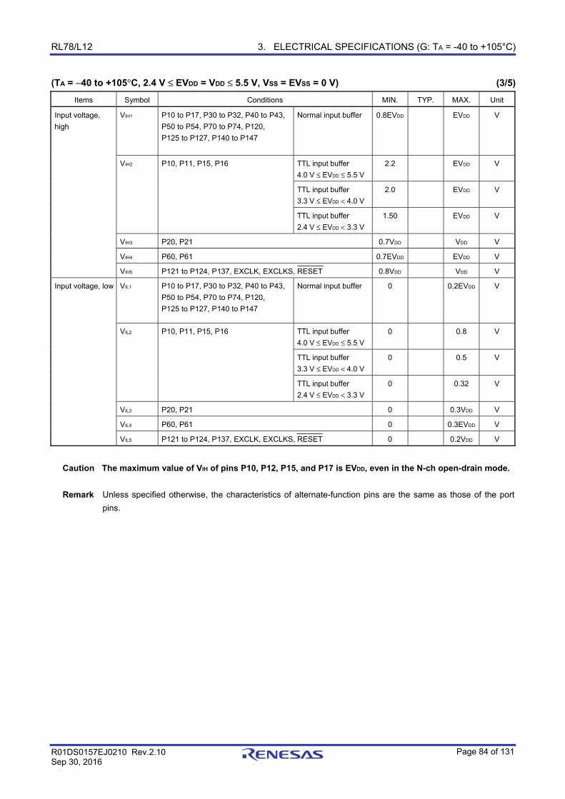
RL78/L12 3. ELECTRICAL SPECIFICATIONS (G: TA = -40 to +105°C)
R01DS0157EJ0210 Rev.2.10 Sep 30, 2016
Page 84 of 131
(TA = −40 to +105°C, 2.4 V ≤ EVDD = VDD ≤ 5.5 V, VSS = EVSS = 0 V) (3/5) Items Symbol Conditions MIN. TYP. MAX. Unit
Input voltage,
high
VIH1 P10 to P17, P30 to P32, P40 to P43,
P50 to P54, P70 to P74, P120,
P125 to P127, P140 to P147
Normal input buffer
0.8EVDD EVDD V
VIH2 P10, P11, P15, P16 TTL input buffer
4.0 V ≤ EVDD ≤ 5.5 V
2.2 EVDD V
TTL input buffer
3.3 V ≤ EVDD < 4.0 V
2.0 EVDD V
TTL input buffer
2.4 V ≤ EVDD < 3.3 V
1.50 EVDD V
VIH3 P20, P21 0.7VDD VDD V
VIH4 P60, P61 0.7EVDD EVDD V
VIH5 P121 to P124, P137, EXCLK, EXCLKS, RESET 0.8VDD VDD V
Input voltage, low VIL1 P10 to P17, P30 to P32, P40 to P43,
P50 to P54, P70 to P74, P120,
P125 to P127, P140 to P147
Normal input buffer
0 0.2EVDD V
VIL2 P10, P11, P15, P16 TTL input buffer
4.0 V ≤ EVDD ≤ 5.5 V
0 0.8 V
TTL input buffer
3.3 V ≤ EVDD < 4.0 V
0 0.5 V
TTL input buffer
2.4 V ≤ EVDD < 3.3 V
0 0.32 V
VIL3 P20, P21 0 0.3VDD V
VIL4 P60, P61 0 0.3EVDD V
VIL5 P121 to P124, P137, EXCLK, EXCLKS, RESET 0 0.2VDD V
Caution The maximum value of VIH of pins P10, P12, P15, and P17 is EVDD, even in the N-ch open-drain mode.
Remark Unless specified otherwise, the characteristics of alternate-function pins are the same as those of the port
pins.
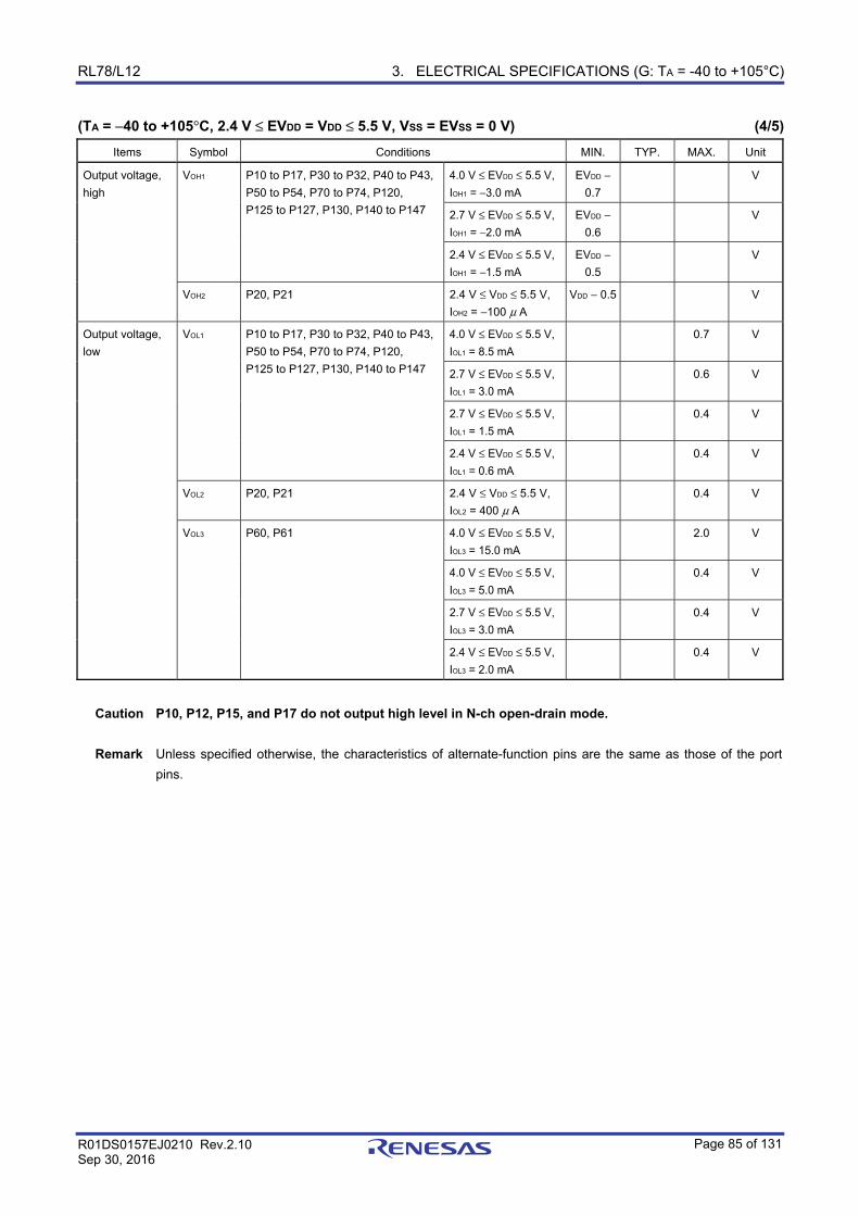
RL78/L12 3. ELECTRICAL SPECIFICATIONS (G: TA = -40 to +105°C)
R01DS0157EJ0210 Rev.2.10 Sep 30, 2016
Page 85 of 131
(TA = −40 to +105°C, 2.4 V ≤ EVDD = VDD ≤ 5.5 V, VSS = EVSS = 0 V) (4/5) Items Symbol Conditions MIN. TYP. MAX. Unit
Output voltage,
high
VOH1 P10 to P17, P30 to P32, P40 to P43,
P50 to P54, P70 to P74, P120,
P125 to P127, P130, P140 to P147
4.0 V ≤ EVDD ≤ 5.5 V,
IOH1 = −3.0 mA
EVDD −
0.7
V
2.7 V ≤ EVDD ≤ 5.5 V,
IOH1 = −2.0 mA
EVDD −
0.6
V
2.4 V ≤ EVDD ≤ 5.5 V,
IOH1 = −1.5 mA
EVDD −
0.5
V
VOH2 P20, P21 2.4 V ≤ VDD ≤ 5.5 V,
IOH2 = −100 μ A
VDD − 0.5 V
Output voltage,
low
VOL1 P10 to P17, P30 to P32, P40 to P43,
P50 to P54, P70 to P74, P120,
P125 to P127, P130, P140 to P147
4.0 V ≤ EVDD ≤ 5.5 V,
IOL1 = 8.5 mA
0.7 V
2.7 V ≤ EVDD ≤ 5.5 V,
IOL1 = 3.0 mA
0.6 V
2.7 V ≤ EVDD ≤ 5.5 V,
IOL1 = 1.5 mA
0.4 V
2.4 V ≤ EVDD ≤ 5.5 V,
IOL1 = 0.6 mA
0.4 V
VOL2 P20, P21 2.4 V ≤ VDD ≤ 5.5 V,
IOL2 = 400 μ A
0.4 V
VOL3 P60, P61 4.0 V ≤ EVDD ≤ 5.5 V,
IOL3 = 15.0 mA
2.0 V
4.0 V ≤ EVDD ≤ 5.5 V,
IOL3 = 5.0 mA
0.4 V
2.7 V ≤ EVDD ≤ 5.5 V,
IOL3 = 3.0 mA
0.4 V
2.4 V ≤ EVDD ≤ 5.5 V,
IOL3 = 2.0 mA
0.4 V
Caution P10, P12, P15, and P17 do not output high level in N-ch open-drain mode.
Remark Unless specified otherwise, the characteristics of alternate-function pins are the same as those of the port
pins.
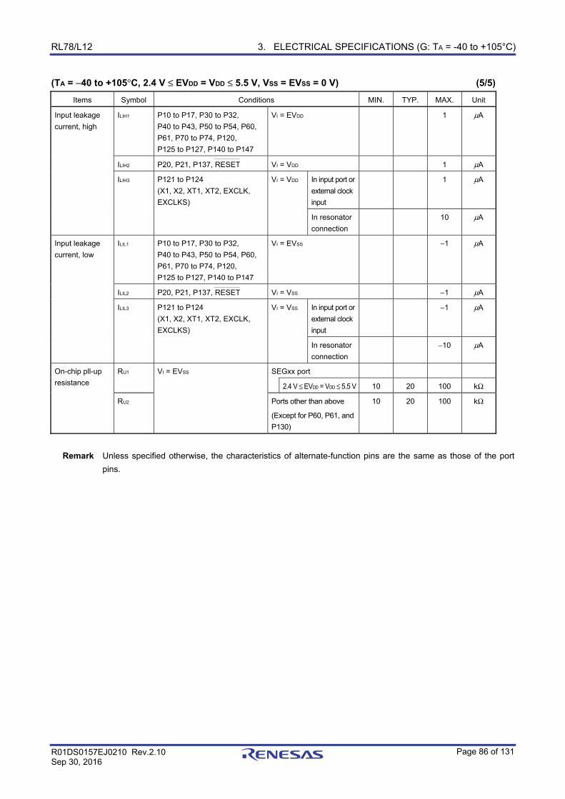
RL78/L12 3. ELECTRICAL SPECIFICATIONS (G: TA = -40 to +105°C)
R01DS0157EJ0210 Rev.2.10 Sep 30, 2016
Page 86 of 131
(TA = −40 to +105°C, 2.4 V ≤ EVDD = VDD ≤ 5.5 V, VSS = EVSS = 0 V) (5/5) Items Symbol Conditions MIN. TYP. MAX. Unit
Input leakage
current, high
ILIH1 P10 to P17, P30 to P32,
P40 to P43, P50 to P54, P60,
P61, P70 to P74, P120,
P125 to P127, P140 to P147
VI = EVDD 1 μA
ILIH2 P20, P21, P137, RESET VI = VDD 1 μA
ILIH3 P121 to P124
(X1, X2, XT1, XT2, EXCLK,
EXCLKS)
VI = VDD In input port or
external clock
input
1 μA
In resonator
connection
10 μA
Input leakage
current, low
ILIL1 P10 to P17, P30 to P32,
P40 to P43, P50 to P54, P60,
P61, P70 to P74, P120,
P125 to P127, P140 to P147
VI = EVSS −1 μA
ILIL2 P20, P21, P137, RESET VI = VSS −1 μA
ILIL3 P121 to P124
(X1, X2, XT1, XT2, EXCLK,
EXCLKS)
VI = VSS In input port or
external clock
input
−1 μA
In resonator
connection
−10 μA
On-chip pll-up
resistance
RU1 VI = EVSS SEGxx port
2.4 V ≤ EVDD = VDD ≤ 5.5 V 10 20 100 kΩ
RU2 Ports other than above
(Except for P60, P61, and
P130)
10 20 100 kΩ
Remark Unless specified otherwise, the characteristics of alternate-function pins are the same as those of the port
pins.
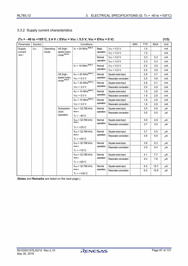
RL78/L12 3. ELECTRICAL SPECIFICATIONS (G: TA = -40 to +105°C)
R01DS0157EJ0210 Rev.2.10 Sep 30, 2016
Page 87 of 131
3.3.2 Supply current characteristics (TA = −40 to +105°C, 2.4 V ≤ EVDD = VDD ≤ 5.5 V, VSS = EVSS = 0 V) (1/3) Parameter Symbol Conditions MIN. TYP. MAX. Unit
Supply current Note 1
IDD1 Operating mode
HS (high-speed main) mode Note 5
fIH = 24 MHz Note 3 Basic operation
VDD = 5.0 V 1.5 mA
VDD = 3.0 V 1.5 mA
Normal operation
VDD = 5.0 V 3.3 5.3 mA
VDD = 3.0 V 3.3 5.3 mA
fIH = 16 MHz Note 3 Normal operation
VDD = 5.0 V 2.5 3.9 mA VDD = 3.0 V 2.5 3.9 mA
HS (high-speed main) mode Note 5
fMX = 20 MHzNote 2,
VDD = 5.0 V
Normal operation
Square wave input 2.8 4.7 mA
Resonator connection 3.0 4.8 mA
fMX = 20 MHzNote 2,
VDD = 3.0 V
Normal operation
Square wave input 2.8 4.7 mA Resonator connection 3.0 4.8 mA
fMX = 10 MHzNote 2,
VDD = 5.0 V
Normal operation
Square wave input 1.8 2.8 mA Resonator connection 1.8 2.8 mA
fMX = 10 MHzNote 2,
VDD = 3.0 V
Normal operation
Square wave input 1.8 2.8 mA Resonator connection 1.8 2.8 mA
Subsystem clock operation
fSUB = 32.768 kHz Note 4
TA = −40°C
Normal operation
Square wave input 3.5 4.9 μA
Resonator connection 3.6 5.0 μA
fSUB = 32.768 kHz
Note 4
TA = +25°C
Normal operation
Square wave input 3.6 4.9 μA
Resonator connection 3.7 5.0 μA
fSUB = 32.768 kHz Note 4
TA = +50°C
Normal operation
Square wave input 3.7 5.5 μA
Resonator connection 3.8 5.6 μA
fSUB = 32.768 kHz Note 4
TA = +70°C
Normal operation
Square wave input 3.8 6.3 μA
Resonator connection 3.9 6.4 μA
fSUB = 32.768 kHz Note 4
TA = +85°C
Normal operation
Square wave input 4.1 7.7 μA
Resonator connection 4.2 7.8 μA
fSUB = 32.768 kHz Note 4
TA = +105°C
Normal operation
Square wave input 6.4 19.7 μA
Resonator connection 6.5 19.8 μA
(Notes and Remarks are listed on the next page.)
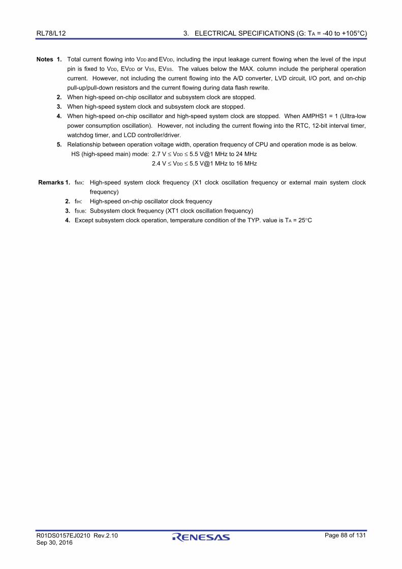
RL78/L12 3. ELECTRICAL SPECIFICATIONS (G: TA = -40 to +105°C)
R01DS0157EJ0210 Rev.2.10 Sep 30, 2016
Page 88 of 131
Notes 1. Total current flowing into VDD and EVDD, including the input leakage current flowing when the level of the input
pin is fixed to VDD, EVDD or VSS, EVSS. The values below the MAX. column include the peripheral operation
current. However, not including the current flowing into the A/D converter, LVD circuit, I/O port, and on-chip
pull-up/pull-down resistors and the current flowing during data flash rewrite.
2. When high-speed on-chip oscillator and subsystem clock are stopped.
3. When high-speed system clock and subsystem clock are stopped.
4. When high-speed on-chip oscillator and high-speed system clock are stopped. When AMPHS1 = 1 (Ultra-low
power consumption oscillation). However, not including the current flowing into the RTC, 12-bit interval timer,
watchdog timer, and LCD controller/driver.
5. Relationship between operation voltage width, operation frequency of CPU and operation mode is as below.
HS (high-speed main) mode: 2.7 V ≤ VDD ≤ 5.5 V@1 MHz to 24 MHz
2.4 V ≤ VDD ≤ 5.5 V@1 MHz to 16 MHz
Remarks 1. fMX: High-speed system clock frequency (X1 clock oscillation frequency or external main system clock
frequency)
2. fIH: High-speed on-chip oscillator clock frequency
3. fSUB: Subsystem clock frequency (XT1 clock oscillation frequency)
4. Except subsystem clock operation, temperature condition of the TYP. value is TA = 25°C
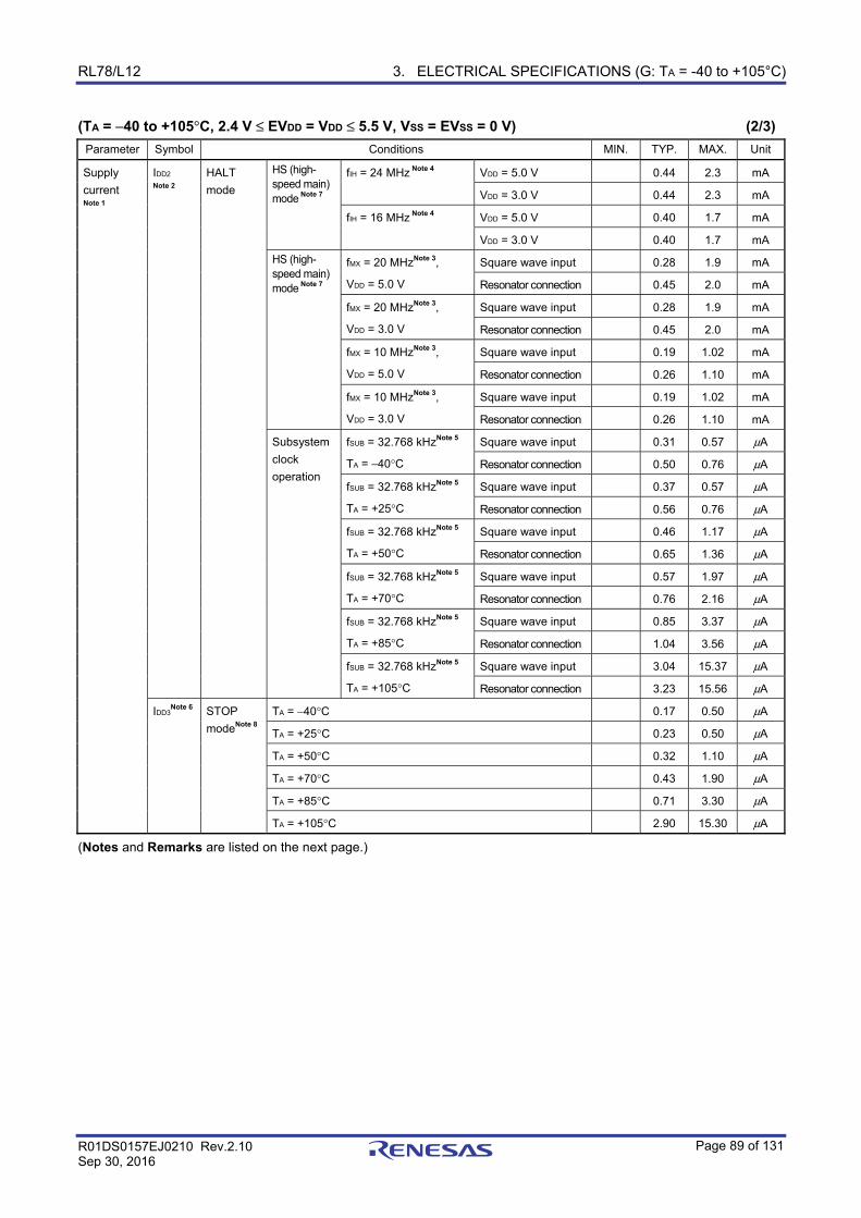
RL78/L12 3. ELECTRICAL SPECIFICATIONS (G: TA = -40 to +105°C)
R01DS0157EJ0210 Rev.2.10 Sep 30, 2016
Page 89 of 131
(TA = −40 to +105°C, 2.4 V ≤ EVDD = VDD ≤ 5.5 V, VSS = EVSS = 0 V) (2/3) Parameter Symbol Conditions MIN. TYP. MAX. Unit
Supply
current
Note 1
IDD2
Note 2
HALT
mode
HS (high-speed main) mode Note 7
fIH = 24 MHz Note 4 VDD = 5.0 V 0.44 2.3 mA
VDD = 3.0 V 0.44 2.3 mA
fIH = 16 MHz Note 4 VDD = 5.0 V 0.40 1.7 mA
VDD = 3.0 V 0.40 1.7 mA
HS (high-speed main) mode Note 7
fMX = 20 MHzNote 3,
VDD = 5.0 V
Square wave input 0.28 1.9 mA
Resonator connection 0.45 2.0 mA
fMX = 20 MHzNote 3,
VDD = 3.0 V
Square wave input 0.28 1.9 mA
Resonator connection 0.45 2.0 mA
fMX = 10 MHzNote 3,
VDD = 5.0 V
Square wave input 0.19 1.02 mA
Resonator connection 0.26 1.10 mA
fMX = 10 MHzNote 3,
VDD = 3.0 V
Square wave input 0.19 1.02 mA
Resonator connection 0.26 1.10 mA
Subsystem
clock
operation
fSUB = 32.768 kHzNote 5
TA = −40°C
Square wave input 0.31 0.57 μA
Resonator connection 0.50 0.76 μA
fSUB = 32.768 kHzNote 5
TA = +25°C
Square wave input 0.37 0.57 μA
Resonator connection 0.56 0.76 μA
fSUB = 32.768 kHzNote 5
TA = +50°C
Square wave input 0.46 1.17 μA
Resonator connection 0.65 1.36 μA
fSUB = 32.768 kHzNote 5
TA = +70°C
Square wave input 0.57 1.97 μA
Resonator connection 0.76 2.16 μA
fSUB = 32.768 kHzNote 5
TA = +85°C
Square wave input 0.85 3.37 μA
Resonator connection 1.04 3.56 μA
fSUB = 32.768 kHzNote 5
TA = +105°C
Square wave input 3.04 15.37 μA
Resonator connection 3.23 15.56 μA
IDD3Note 6 STOP
modeNote 8TA = −40°C 0.17 0.50 μA
TA = +25°C 0.23 0.50 μA
TA = +50°C 0.32 1.10 μA
TA = +70°C 0.43 1.90 μA
TA = +85°C 0.71 3.30 μA
TA = +105°C 2.90 15.30 μA
(Notes and Remarks are listed on the next page.)
RL78/L12 3. ELECTRICAL SPECIFICATIONS (G: TA = -40 to +105°C)
R01DS0157EJ0210 Rev.2.10 Sep 30, 2016
Page 90 of 131
Notes 1. Total current flowing into VDD and EVDD, including the input leakage current flowing when the level of the input
pin is fixed to VDD, EVDD or VSS, EVSS. The values below the MAX. column include the peripheral operation
current. However, not including the current flowing into the A/D converter, LVD circuit, I/O port, and on-chip
pull-up/pull-down resistors and the current flowing during data flash rewrite.
2. During HALT instruction execution by flash memory.
3. When high-speed on-chip oscillator and subsystem clock are stopped.
4. When high-speed system clock and subsystem clock are stopped.
5. When high-speed on-chip oscillator and high-speed system clock are stopped. When RTCLPC = 1 and setting
ultra-low current consumption (AMPHS1 = 1). The current flowing into the RTC is included. However, not
including the current flowing into the 12-bit interval timer, watchdog timer, and LCD controller/driver.
6. Not including the current flowing into the RTC, 12-bit interval timer, and watchdog timer.
7. Relationship between operation voltage width, operation frequency of CPU and operation mode is as below.
HS (high-speed main) mode: 2.7 V ≤ VDD ≤ 5.5 V@1 MHz to 24 MHz
2.4 V ≤ VDD ≤ 5.5 V@1 MHz to 16 MHz
8. Regarding the value for current operate the subsystem clock in STOP mode, refer to that in HALT mode.
Remarks 1. fMX: High-speed system clock frequency (X1 clock oscillation frequency or external main system clock
frequency)
2. fIH: High-speed on-chip oscillator clock frequency
3. fSUB: Subsystem clock frequency (XT1 clock oscillation frequency)
4. Except subsystem clock operation and STOP mode, temperature condition of the TYP. value is TA = 25°C
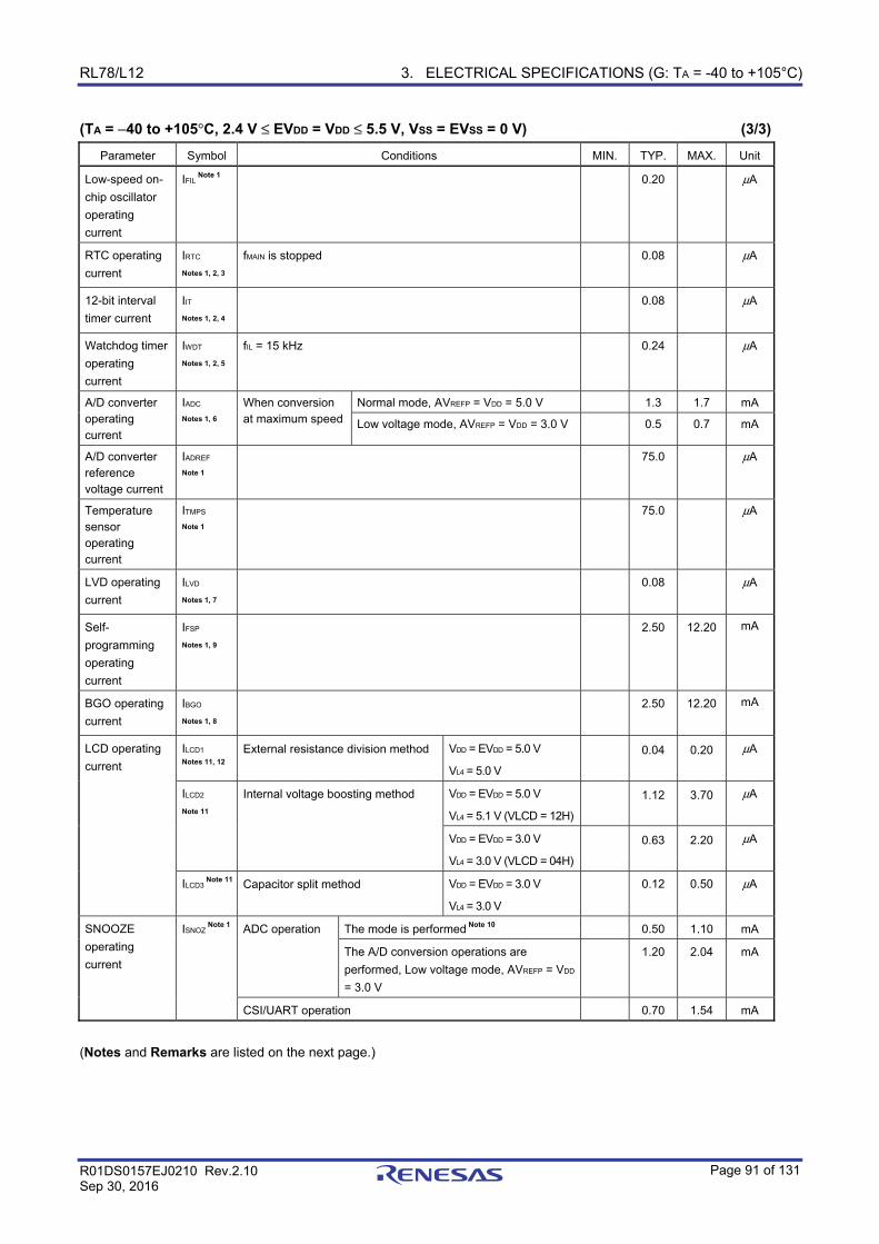
RL78/L12 3. ELECTRICAL SPECIFICATIONS (G: TA = -40 to +105°C)
R01DS0157EJ0210 Rev.2.10 Sep 30, 2016
Page 91 of 131
(TA = −40 to +105°C, 2.4 V ≤ EVDD = VDD ≤ 5.5 V, VSS = EVSS = 0 V) (3/3) Parameter Symbol Conditions MIN. TYP. MAX. Unit
Low-speed on-
chip oscillator
operating
current
IFIL Note 1 0.20 μA
RTC operating
current
IRTC
Notes 1, 2, 3
fMAIN is stopped 0.08 μA
12-bit interval
timer current
IIT
Notes 1, 2, 4
0.08 μA
Watchdog timer
operating
current
IWDT
Notes 1, 2, 5
fIL = 15 kHz 0.24 μA
A/D converter operating current
IADC
Notes 1, 6
When conversion at maximum speed
Normal mode, AVREFP = VDD = 5.0 V 1.3 1.7 mA
Low voltage mode, AVREFP = VDD = 3.0 V 0.5 0.7 mA
A/D converter reference voltage current
IADREF
Note 1
75.0 μA
Temperature sensor operating current
ITMPS
Note 1
75.0 μA
LVD operating
current
ILVD
Notes 1, 7
0.08 μA
Self-
programming
operating
current
IFSP
Notes 1, 9
2.50 12.20 mA
BGO operating
current
IBGO
Notes 1, 8
2.50 12.20 mA
LCD operating
current
ILCD1
Notes 11, 12
External resistance division method VDD = EVDD = 5.0 V
VL4 = 5.0 V
0.04 0.20 μA
ILCD2
Note 11
Internal voltage boosting method VDD = EVDD = 5.0 V
VL4 = 5.1 V (VLCD = 12H)
1.12 3.70 μA
VDD = EVDD = 3.0 V
VL4 = 3.0 V (VLCD = 04H)
0.63 2.20 μA
ILCD3 Note 11 Capacitor split method VDD = EVDD = 3.0 V
VL4 = 3.0 V
0.12 0.50 μA
SNOOZE
operating
current
ISNOZ Note 1 ADC operation The mode is performed Note 10 0.50 1.10 mA
The A/D conversion operations are
performed, Low voltage mode, AVREFP = VDD
= 3.0 V
1.20 2.04 mA
CSI/UART operation 0.70 1.54 mA
(Notes and Remarks are listed on the next page.)
RL78/L12 3. ELECTRICAL SPECIFICATIONS (G: TA = -40 to +105°C)
R01DS0157EJ0210 Rev.2.10 Sep 30, 2016
Page 92 of 131
Notes 1. Current flowing to VDD.
2. When high speed on-chip oscillator and high-speed system clock are stopped.
3. Current flowing only to the real-time clock (RTC) (excluding the operating current of the low-speed on-chip
oscillator and the XT1 oscillator). The supply current of the RL78 microcontrollers is the sum of the values of
either IDD1 or IDD2, and IRTC, when the real-time clock operates in operation mode or HALT mode. When the
low-speed on-chip oscillator is selected, IFIL should be added. IDD2 subsystem clock operation includes the
operational current of the real-time clock.
4. Current flowing only to the 12-bit interval timer (excluding the operating current of the low-speed on-chip
oscillator and the XT1 oscillator). The supply current of the RL78 microcontrollers is the sum of the values of
either IDD1 or IDD2, and IIT, when the 12-bit interval timer operates in operation mode or HALT mode. When the
low-speed on-chip oscillator is selected, IFIL should be added.
5. Current flowing only to the watchdog timer (including the operating current of the low-speed on-chip oscillator).
The supply current of the RL78 microcontrollers is the sum of IDD1, IDD2 or IDD3 and IWDT when the watchdog
timer is in operation.
6. Current flowing only to the A/D converter. The supply current of the RL78 microcontrollers is the sum of IDD1 or
IDD2 and IADC when the A/D converter operates in an operation mode or the HALT mode.
7. Current flowing only to the LVD circuit. The supply current of the RL78 microcontrollers is the sum of IDD1, IDD2
or IDD3 and ILVD when the LVD circuit is in operation.
8. Current flowing only during data flash rewrite.
9. Current flowing only during self programming.
10. For shift time to the SNOOZE mode.
11. Current flowing only to the LCD controller/driver. The supply current value of the RL78 microcontrollers is the
sum of the LCD operating current (ILCD1, ILCD2 or ILCD3) to the supply current (IDD1 or IDD2) when the LCD
controller/driver operates in an operation mode or HALT mode. Not including the current that flows through the
LCD panel.
The TYP. value and MAX. value are following conditions.
• When fSUB is selected for system clock, LCD clock = 128 Hz (LCDC0 = 07H)
• 4-Time-Slice, 1/3 Bias Method
12. Not including the current that flows through the external divider resistor when the external resistance division
method is used.
Remarks 1. fIL: Low-speed on-chip oscillator clock frequency
2. fSUB: Subsystem clock frequency (XT1 clock oscillation frequency)
3. fCLK: CPU/peripheral hardware clock frequency
4. Temperature condition of the TYP. value is TA = 25°C
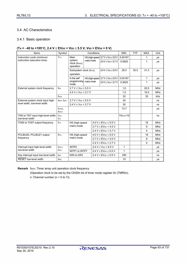
RL78/L12 3. ELECTRICAL SPECIFICATIONS (G: TA = -40 to +105°C)
R01DS0157EJ0210 Rev.2.10 Sep 30, 2016
Page 93 of 131
3.4 AC Characteristics
3.4.1 Basic operation
(TA = −40 to +105°C, 2.4 V ≤ EVDD = VDD ≤ 5.5 V, VSS = EVSS = 0 V) Items Symbol Conditions MIN. TYP. MAX. Unit
Instruction cycle (minimum instruction execution time)
TCY Main system clock (fMAIN) operation
HS (high-speed main) mode
2.7 V ≤ VDD ≤ 5.5 V 0.04167 1 μs
2.4 V ≤ VDD < 2.7 V 0.0625 1 μs
Subsystem clock (fSUB)
operation
2.4 V ≤ VDD ≤ 5.5 V 28.5 30.5 31.3 μs
In the self programming mode
HS (high-speed main) mode
2.7 V ≤ VDD ≤ 5.5 V 0.04167 1 μs
2.4 V ≤ VDD < 2.7 V 0.0625 1 μs
External system clock frequency fEX 2.7 V ≤ VDD ≤ 5.5 V 1.0 20.0 MHz 2.4 V ≤ VDD < 2.7 V 1.0 16.0 MHz
fEXS 32 35 kHz
External system clock input high-level width, low-level width
tEXH, tEXL 2.7 V ≤ VDD ≤ 5.5 V 24 ns 2.4 V ≤ VDD < 2.7 V 30 ns
tEXHS, tEXLS
13.7 μs
TI00 to TI07 input high-level width, low-level width
tTIH, tTIL
1/fMCK+10 ns
TO00 to TO07 output frequency fTO HS (high-speed main) mode
4.0 V ≤ EVDD ≤ 5.5 V 16 MHz
2.7 V ≤ EVDD < 4.0 V 8 MHz
2.4 V ≤ EVDD < 2.7 V 4 MHz
PCLBUZ0, PCLBUZ1 output frequency
fPCL HS (high-speed main) mode
4.0 V ≤ EVDD ≤ 5.5 V 16 MHz
2.7 V ≤ EVDD < 4.0 V 8 MHz
2.4 V ≤ EVDD < 2.7 V 4 MHz
Interrupt input high-level width, low-level width
tINTH, tINTL
INTP0 2.4 V ≤ VDD ≤ 5.5 V 1 μs
INTP1 to INTP7 2.4 V ≤ EVDD ≤ 5.5 V 1 μs
Key interrupt input low-level width tKR KR0 to KR3 2.4 V ≤ EVDD ≤ 5.5 V 250 ns RESET low-level width tRSL 10 μs
Remark fMCK: Timer array unit operation clock frequency
(Operation clock to be set by the CKS0n bit of timer mode register 0n (TMR0n).
n: Channel number (n = 0 to 7))
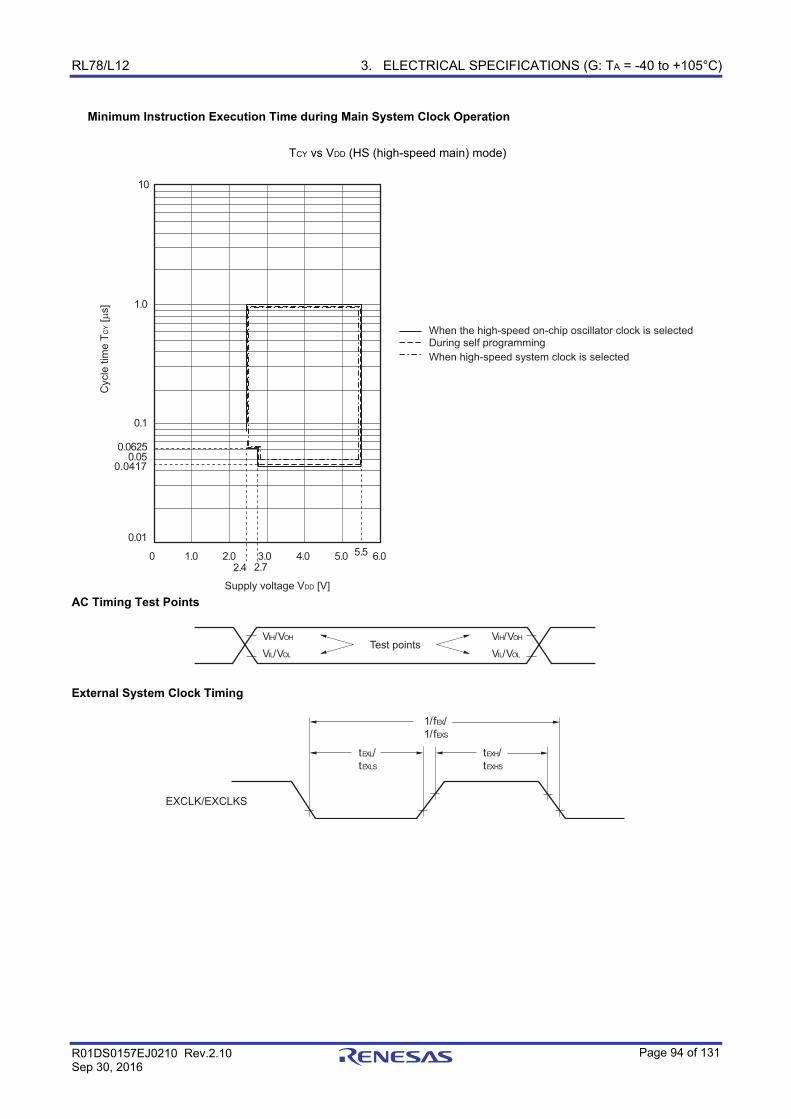
RL78/L12 3. ELECTRICAL SPECIFICATIONS (G: TA = -40 to +105°C)
R01DS0157EJ0210 Rev.2.10 Sep 30, 2016
Page 94 of 131
Minimum Instruction Execution Time during Main System Clock Operation
TCY vs VDD (HS (high-speed main) mode)
1.0
0.1
0
10
1.0 2.0 3.0 4.0 5.0 6.05.5
2.7
0.01
2.4
0.06250.05
0.0417
When the high-speed on-chip oscillator clock is selectedDuring self programming
When high-speed system clock is selected
Cycle
tim
e T
CY [µ
s]
Supply voltage VDD [V] AC Timing Test Points
VIH/VOH
VIL/VOL
VIH/VOH
VIL/VOL
Test points
External System Clock Timing
1/fEX/
1/fEXS
tEXL/
tEXLS
tEXH/
tEXHS
EXCLK/EXCLKS
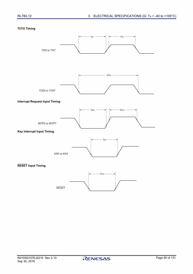
RL78/L12 3. ELECTRICAL SPECIFICATIONS (G: TA = -40 to +105°C)
R01DS0157EJ0210 Rev.2.10 Sep 30, 2016
Page 95 of 131
TI/TO Timing
tTIL tTIH
1/fTO
TI00 to TI07
TO00 to TO07
Interrupt Request Input Timing
tINTL tINTH
INTP0 to INTP7
Key Interrupt Input Timing
tKR
KR0 to KR3
RESET Input Timing
RESET
tRSL
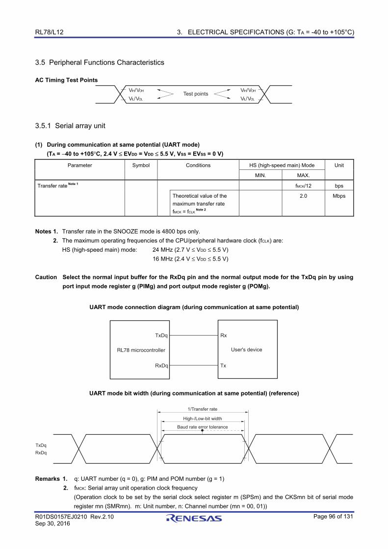
RL78/L12 3. ELECTRICAL SPECIFICATIONS (G: TA = -40 to +105°C)
R01DS0157EJ0210 Rev.2.10 Sep 30, 2016
Page 96 of 131
3.5 Peripheral Functions Characteristics AC Timing Test Points
VIH/VOH
VIL/VOL
VIH/VOH
VIL/VOL
Test points
3.5.1 Serial array unit (1) During communication at same potential (UART mode)
(TA = −40 to +105°C, 2.4 V ≤ EVDD = VDD ≤ 5.5 V, VSS = EVSS = 0 V)
Parameter Symbol Conditions HS (high-speed main) Mode Unit
MIN. MAX.
Transfer rate Note 1 fMCK/12 bps
Theoretical value of the
maximum transfer rate
fMCK = fCLK Note 2
2.0 Mbps
Notes 1. Transfer rate in the SNOOZE mode is 4800 bps only.
2. The maximum operating frequencies of the CPU/peripheral hardware clock (fCLK) are:
HS (high-speed main) mode: 24 MHz (2.7 V ≤ VDD ≤ 5.5 V)
16 MHz (2.4 V ≤ VDD ≤ 5.5 V)
Caution Select the normal input buffer for the RxDq pin and the normal output mode for the TxDq pin by using port input mode register g (PIMg) and port output mode register g (POMg).
UART mode connection diagram (during communication at same potential)
User's device
TxDq
RxDq
Rx
Tx
RL78 microcontroller
UART mode bit width (during communication at same potential) (reference)
Baud rate error tolerance
High-/Low-bit width
1/Transfer rate
TxDq
RxDq
Remarks 1. q: UART number (q = 0), g: PIM and POM number (g = 1)
2. fMCK: Serial array unit operation clock frequency
(Operation clock to be set by the serial clock select register m (SPSm) and the CKSmn bit of serial mode
register mn (SMRmn). m: Unit number, n: Channel number (mn = 00, 01))
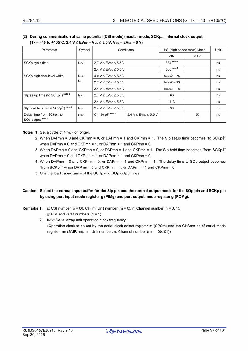
RL78/L12 3. ELECTRICAL SPECIFICATIONS (G: TA = -40 to +105°C)
R01DS0157EJ0210 Rev.2.10 Sep 30, 2016
Page 97 of 131
(2) During communication at same potential (CSI mode) (master mode, SCKp... internal clock output) (TA = −40 to +105°C, 2.4 V ≤ EVDD = VDD ≤ 5.5 V, VSS = EVSS = 0 V)
Notes 1. Set a cycle of 4/fMCK or longer.
2. When DAPmn = 0 and CKPmn = 0, or DAPmn = 1 and CKPmn = 1. The SIp setup time becomes “to SCKp↓”
when DAPmn = 0 and CKPmn = 1, or DAPmn = 1 and CKPmn = 0.
3. When DAPmn = 0 and CKPmn = 0, or DAPmn = 1 and CKPmn = 1. The SIp hold time becomes “from SCKp↓”
when DAPmn = 0 and CKPmn = 1, or DAPmn = 1 and CKPmn = 0.
4. When DAPmn = 0 and CKPmn = 0, or DAPmn = 1 and CKPmn = 1. The delay time to SOp output becomes
“from SCKp↑” when DAPmn = 0 and CKPmn = 1, or DAPmn = 1 and CKPmn = 0.
5. C is the load capacitance of the SCKp and SOp output lines.
Caution Select the normal input buffer for the SIp pin and the normal output mode for the SOp pin and SCKp pin by using port input mode register g (PIMg) and port output mode register g (POMg).
Remarks 1. p: CSI number (p = 00, 01), m: Unit number (m = 0), n: Channel number (n = 0, 1),
g: PIM and POM numbers (g = 1)
2. fMCK: Serial array unit operation clock frequency
(Operation clock to be set by the serial clock select register m (SPSm) and the CKSmn bit of serial mode
register mn (SMRmn). m: Unit number, n: Channel number (mn = 00, 01))
Parameter Symbol Conditions HS (high-speed main) Mode Unit
MIN. MAX.
SCKp cycle time tKCY1 2.7 V ≤ EVDD ≤ 5.5 V 334 Note 1 ns
2.4 V ≤ EVDD ≤ 5.5 V 500 Note 1 ns
SCKp high-/low-level width tKH1,
tKL1
4.0 V ≤ EVDD ≤ 5.5 V tKCY1/2 − 24 ns
2.7 V ≤ EVDD ≤ 5.5 V tKCY1/2 − 36 ns
2.4 V ≤ EVDD ≤ 5.5 V tKCY1/2 − 76 ns
SIp setup time (to SCKp↑) Note 2 tSIK1 2.7 V ≤ EVDD ≤ 5.5 V 66 ns
2.4 V ≤ EVDD ≤ 5.5 V 113 ns
SIp hold time (from SCKp↑) Note 3 tKSI1 2.4 V ≤ EVDD ≤ 5.5 V 38 ns
Delay time from SCKp↓ to
SOp output Note 4
tKSO1 C = 30 pF Note 5 2.4 V ≤ EVDD ≤ 5.5 V 50 ns
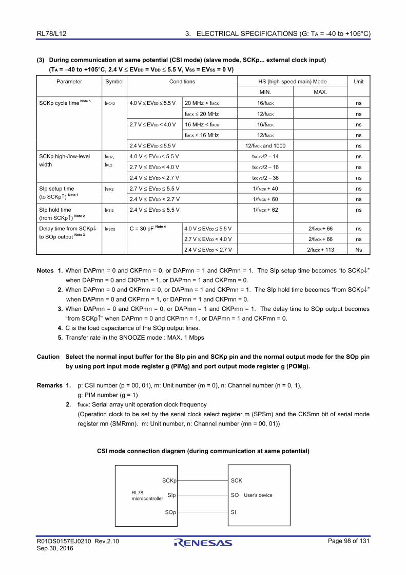
RL78/L12 3. ELECTRICAL SPECIFICATIONS (G: TA = -40 to +105°C)
R01DS0157EJ0210 Rev.2.10 Sep 30, 2016
Page 98 of 131
(3) During communication at same potential (CSI mode) (slave mode, SCKp... external clock input) (TA = −40 to +105°C, 2.4 V ≤ EVDD = VDD ≤ 5.5 V, VSS = EVSS = 0 V)
Parameter Symbol Conditions HS (high-speed main) Mode Unit
MIN. MAX.
SCKp cycle time Note 5 tKCY2 4.0 V ≤ EVDD ≤ 5.5 V 20 MHz < fMCK 16/fMCK ns
fMCK ≤ 20 MHz 12/fMCK ns
2.7 V ≤ EVDD < 4.0 V 16 MHz < fMCK 16/fMCK ns
fMCK ≤ 16 MHz 12/fMCK ns
2.4 V ≤ EVDD ≤ 5.5 V 12/fMCK and 1000 ns
SCKp high-/low-level
width
tKH2,
tKL2
4.0 V ≤ EVDD ≤ 5.5 V tKCY2/2 − 14 ns
2.7 V ≤ EVDD < 4.0 V tKCY2/2 − 16 ns
2.4 V ≤ EVDD < 2.7 V tKCY2/2 − 36 ns
SIp setup time
(to SCKp↑) Note 1
tSIK2 2.7 V ≤ EVDD ≤ 5.5 V 1/fMCK + 40 ns
2.4 V ≤ EVDD < 2.7 V 1/fMCK + 60 ns
SIp hold time
(from SCKp↑) Note 2
tKSI2 2.4 V ≤ EVDD ≤ 5.5 V 1/fMCK + 62 ns
Delay time from SCKp↓
to SOp output Note 3
tKSO2 C = 30 pF Note 4 4.0 V ≤ EVDD ≤ 5.5 V 2/fMCK + 66 ns
2.7 V ≤ EVDD < 4.0 V 2/fMCK + 66 ns
2.4 V ≤ EVDD < 2.7 V 2/fMCK + 113 Ns
Notes 1. When DAPmn = 0 and CKPmn = 0, or DAPmn = 1 and CKPmn = 1. The SIp setup time becomes “to SCKp↓”
when DAPmn = 0 and CKPmn = 1, or DAPmn = 1 and CKPmn = 0.
2. When DAPmn = 0 and CKPmn = 0, or DAPmn = 1 and CKPmn = 1. The SIp hold time becomes “from SCKp↓”
when DAPmn = 0 and CKPmn = 1, or DAPmn = 1 and CKPmn = 0.
3. When DAPmn = 0 and CKPmn = 0, or DAPmn = 1 and CKPmn = 1. The delay time to SOp output becomes
“from SCKp↑” when DAPmn = 0 and CKPmn = 1, or DAPmn = 1 and CKPmn = 0.
4. C is the load capacitance of the SOp output lines.
5. Transfer rate in the SNOOZE mode : MAX. 1 Mbps
Caution Select the normal input buffer for the SIp pin and SCKp pin and the normal output mode for the SOp pin by using port input mode register g (PIMg) and port output mode register g (POMg).
Remarks 1. p: CSI number (p = 00, 01), m: Unit number (m = 0), n: Channel number (n = 0, 1),
g: PIM number (g = 1)
2. fMCK: Serial array unit operation clock frequency
(Operation clock to be set by the serial clock select register m (SPSm) and the CKSmn bit of serial mode
register mn (SMRmn). m: Unit number, n: Channel number (mn = 00, 01))
CSI mode connection diagram (during communication at same potential)
RL78
microcontroller
SCKp
SOp
SCK
SI
User's deviceSIp SO
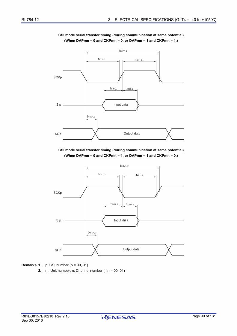
RL78/L12 3. ELECTRICAL SPECIFICATIONS (G: TA = -40 to +105°C)
R01DS0157EJ0210 Rev.2.10 Sep 30, 2016
Page 99 of 131
CSI mode serial transfer timing (during communication at same potential) (When DAPmn = 0 and CKPmn = 0, or DAPmn = 1 and CKPmn = 1.)
SIp Input data
Output dataSOp
tKCY1, 2
tKL1, 2 tKH1, 2
tSIK1, 2 tKSI1, 2
tKSO1, 2
SCKp
CSI mode serial transfer timing (during communication at same potential) (When DAPmn = 0 and CKPmn = 1, or DAPmn = 1 and CKPmn = 0.)
SIp Input data
Output dataSOp
tKCY1, 2
tKH1, 2 tKL1, 2
tSIK1, 2 tKSI1, 2
tKSO1, 2
SCKp
Remarks 1. p: CSI number (p = 00, 01)
2. m: Unit number, n: Channel number (mn = 00, 01)
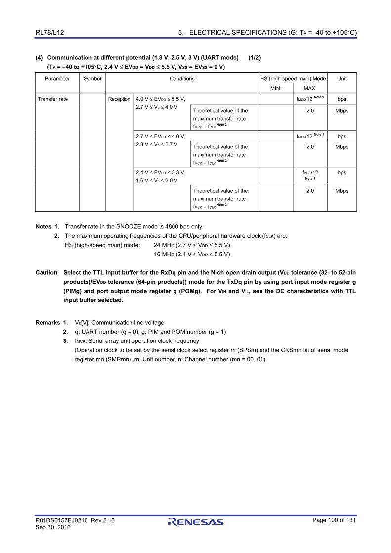
RL78/L12 3. ELECTRICAL SPECIFICATIONS (G: TA = -40 to +105°C)
R01DS0157EJ0210 Rev.2.10 Sep 30, 2016
Page 100 of 131
(4) Communication at different potential (1.8 V, 2.5 V, 3 V) (UART mode) (1/2) (TA = −40 to +105°C, 2.4 V ≤ EVDD = VDD ≤ 5.5 V, VSS = EVSS = 0 V)
Parameter Symbol Conditions HS (high-speed main) Mode Unit
MIN. MAX.
Transfer rate Reception 4.0 V ≤ EVDD ≤ 5.5 V,
2.7 V ≤ Vb ≤ 4.0 V
fMCK/12 Note 1 bps
Theoretical value of the
maximum transfer rate
fMCK = fCLK Note 2
2.0 Mbps
2.7 V ≤ EVDD < 4.0 V,
2.3 V ≤ Vb ≤ 2.7 V
fMCK/12 Note 1 bps
Theoretical value of the
maximum transfer rate
fMCK = fCLK Note 2
2.0 Mbps
2.4 V ≤ EVDD < 3.3 V,
1.6 V ≤ Vb ≤ 2.0 V
fMCK/12 Note 1
bps
Theoretical value of the
maximum transfer rate
fMCK = fCLK Note 2
2.0 Mbps
Notes 1. Transfer rate in the SNOOZE mode is 4800 bps only.
2. The maximum operating frequencies of the CPU/peripheral hardware clock (fCLK) are:
HS (high-speed main) mode: 24 MHz (2.7 V ≤ VDD ≤ 5.5 V)
16 MHz (2.4 V ≤ VDD ≤ 5.5 V) Caution Select the TTL input buffer for the RxDq pin and the N-ch open drain output (VDD tolerance (32- to 52-pin
products)/EVDD tolerance (64-pin products)) mode for the TxDq pin by using port input mode register g (PIMg) and port output mode register g (POMg). For VIH and VIL, see the DC characteristics with TTL input buffer selected.
Remarks 1. Vb[V]: Communication line voltage
2. q: UART number (q = 0), g: PIM and POM number (g = 1)
3. fMCK: Serial array unit operation clock frequency
(Operation clock to be set by the serial clock select register m (SPSm) and the CKSmn bit of serial mode
register mn (SMRmn). m: Unit number, n: Channel number (mn = 00, 01)
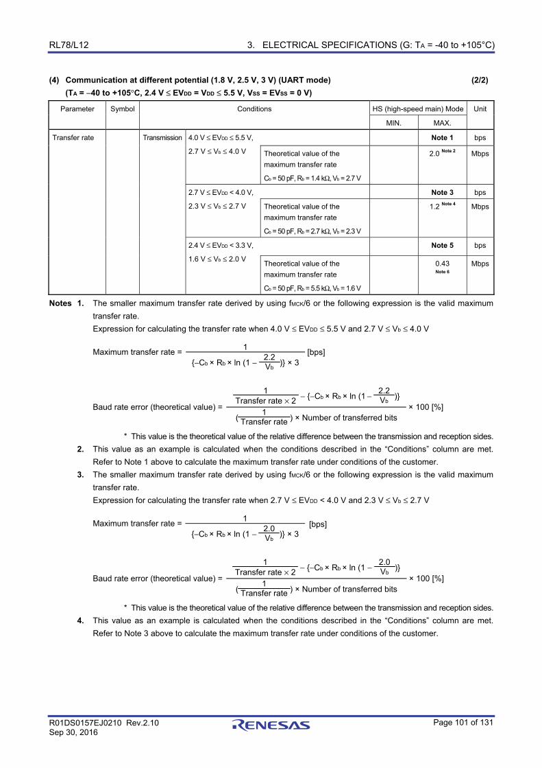
RL78/L12 3. ELECTRICAL SPECIFICATIONS (G: TA = -40 to +105°C)
R01DS0157EJ0210 Rev.2.10 Sep 30, 2016
Page 101 of 131
(4) Communication at different potential (1.8 V, 2.5 V, 3 V) (UART mode) (2/2) (TA = −40 to +105°C, 2.4 V ≤ EVDD = VDD ≤ 5.5 V, VSS = EVSS = 0 V)
Parameter Symbol Conditions HS (high-speed main) Mode Unit
MIN. MAX.
Transfer rate Transmission 4.0 V ≤ EVDD ≤ 5.5 V,
2.7 V ≤ Vb ≤ 4.0 V
Note 1 bps
Theoretical value of the
maximum transfer rate
Cb = 50 pF, Rb = 1.4 kΩ, Vb = 2.7 V
2.0 Note 2 Mbps
2.7 V ≤ EVDD < 4.0 V,
2.3 V ≤ Vb ≤ 2.7 V
Note 3 bps
Theoretical value of the
maximum transfer rate
Cb = 50 pF, Rb = 2.7 kΩ, Vb = 2.3 V
1.2 Note 4 Mbps
2.4 V ≤ EVDD < 3.3 V,
1.6 V ≤ Vb ≤ 2.0 V
Note 5 bps
Theoretical value of the
maximum transfer rate
Cb = 50 pF, Rb = 5.5 kΩ, Vb = 1.6 V
0.43 Note 6
Mbps
Notes 1. The smaller maximum transfer rate derived by using fMCK/6 or the following expression is the valid maximum
transfer rate.
Expression for calculating the transfer rate when 4.0 V ≤ EVDD ≤ 5.5 V and 2.7 V ≤ Vb ≤ 4.0 V
Maximum transfer rate = 1
[bps] {−Cb × Rb × ln (1 −
2.2 Vb
)} × 3
1
Transfer rate × 2 − {−Cb × Rb × ln (1 −
2.2 Vb
)}
Baud rate error (theoretical value) =
× 100 [%] (
1 Transfer rate ) × Number of transferred bits
* This value is the theoretical value of the relative difference between the transmission and reception sides.
2. This value as an example is calculated when the conditions described in the “Conditions” column are met.
Refer to Note 1 above to calculate the maximum transfer rate under conditions of the customer.
3. The smaller maximum transfer rate derived by using fMCK/6 or the following expression is the valid maximum
transfer rate.
Expression for calculating the transfer rate when 2.7 V ≤ EVDD < 4.0 V and 2.3 V ≤ Vb ≤ 2.7 V
Maximum transfer rate = 1
[bps] {−Cb × Rb × ln (1 −
2.0 Vb
)} × 3
1
Transfer rate × 2 − {−Cb × Rb × ln (1 −
2.0 Vb
)}
Baud rate error (theoretical value) =
× 100 [%] (
1 Transfer rate ) × Number of transferred bits
* This value is the theoretical value of the relative difference between the transmission and reception sides.
4. This value as an example is calculated when the conditions described in the “Conditions” column are met.
Refer to Note 3 above to calculate the maximum transfer rate under conditions of the customer.
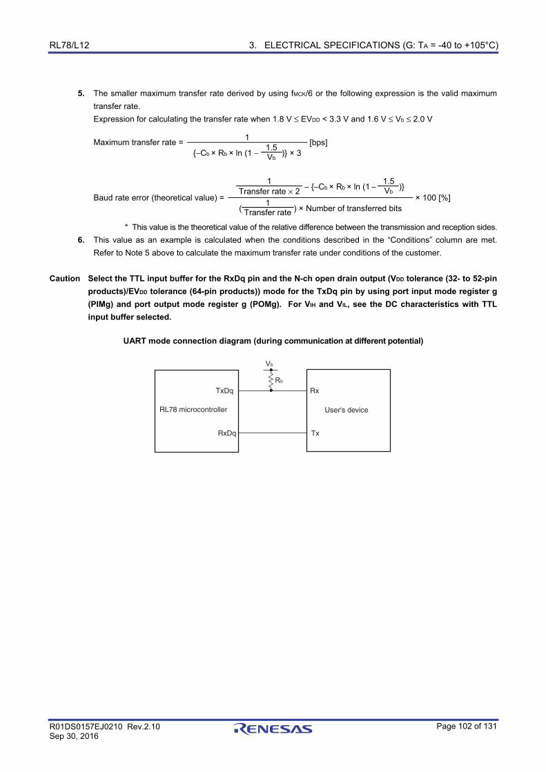
RL78/L12 3. ELECTRICAL SPECIFICATIONS (G: TA = -40 to +105°C)
R01DS0157EJ0210 Rev.2.10 Sep 30, 2016
Page 102 of 131
5. The smaller maximum transfer rate derived by using fMCK/6 or the following expression is the valid maximum
transfer rate.
Expression for calculating the transfer rate when 1.8 V ≤ EVDD < 3.3 V and 1.6 V ≤ Vb ≤ 2.0 V
Maximum transfer rate = 1
[bps] {−Cb × Rb × ln (1 −
1.5 Vb
)} × 3
1
Transfer rate × 2 − {−Cb × Rb × ln (1 −
1.5 Vb
)}
Baud rate error (theoretical value) =
× 100 [%] (
1 Transfer rate ) × Number of transferred bits
* This value is the theoretical value of the relative difference between the transmission and reception sides.
6. This value as an example is calculated when the conditions described in the “Conditions” column are met.
Refer to Note 5 above to calculate the maximum transfer rate under conditions of the customer.
Caution Select the TTL input buffer for the RxDq pin and the N-ch open drain output (VDD tolerance (32- to 52-pin
products)/EVDD tolerance (64-pin products)) mode for the TxDq pin by using port input mode register g (PIMg) and port output mode register g (POMg). For VIH and VIL, see the DC characteristics with TTL input buffer selected.
UART mode connection diagram (during communication at different potential)
TxDq
RxDq
Rx
Tx
Vb
Rb
User's deviceRL78 microcontroller
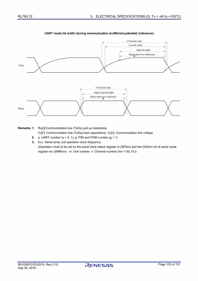
RL78/L12 3. ELECTRICAL SPECIFICATIONS (G: TA = -40 to +105°C)
R01DS0157EJ0210 Rev.2.10 Sep 30, 2016
Page 103 of 131
UART mode bit width (during communication at different potential) (reference)
TxDq
RxDq
Baud rate error tolerance
Baud rate error tolerance
Low-bit width
High-/Low-bit width
High-bit width
1/Transfer rate
1/Transfer rate
Remarks 1. Rb[Ω]:Communication line (TxDq) pull-up resistance,
Cb[F]: Communication line (TxDq) load capacitance, Vb[V]: Communication line voltage
2. q: UART number (q = 0, 1), g: PIM and POM number (g = 1)
3. fMCK: Serial array unit operation clock frequency
(Operation clock to be set by the serial clock select register m (SPSm) and the CKSmn bit of serial mode
register mn (SMRmn). m: Unit number, n: Channel number (mn = 00, 01))
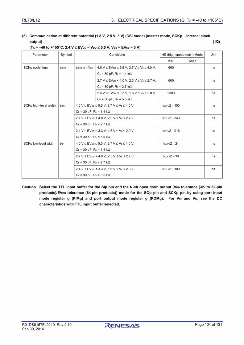
RL78/L12 3. ELECTRICAL SPECIFICATIONS (G: TA = -40 to +105°C)
R01DS0157EJ0210 Rev.2.10 Sep 30, 2016
Page 104 of 131
(5) Communication at different potential (1.8 V, 2.5 V, 3 V) (CSI mode) (master mode, SCKp... internal clock output) (1/2)
(TA = −40 to +105°C, 2.4 V ≤ EVDD = VDD ≤ 5.5 V, VSS = EVSS = 0 V)
Parameter Symbol Conditions HS (high-speed main) Mode Unit
MIN. MAX.
SCKp cycle time tKCY1 tKCY1 ≥ 4/fCLK 4.0 V ≤ EVDD ≤ 5.5 V, 2.7 V ≤ Vb ≤ 4.0 V,
Cb = 30 pF, Rb = 1.4 kΩ
600 ns
2.7 V ≤ EVDD < 4.0 V, 2.3 V ≤ Vb ≤ 2.7 V,
Cb = 30 pF, Rb = 2.7 kΩ
600 ns
2.4 V ≤ EVDD < 3.3 V, 1.6 V ≤ Vb ≤ 2.0 V,
Cb = 30 pF, Rb = 5.5 kΩ
2300 ns
SCKp high-level width tKH1 4.0 V ≤ EVDD ≤ 5.5 V, 2.7 V ≤ Vb ≤ 4.0 V,
Cb = 30 pF, Rb = 1.4 kΩ
tKCY1/2 − 150 ns
2.7 V ≤ EVDD < 4.0 V, 2.3 V ≤ Vb ≤ 2.7 V,
Cb = 30 pF, Rb = 2.7 kΩ
tKCY1/2 − 340 ns
2.4 V ≤ EVDD < 3.3 V, 1.6 V ≤ Vb ≤ 2.0 V,
Cb = 30 pF, Rb = 5.5 kΩ
tKCY1/2 − 916 ns
SCKp low-level width tKL1 4.0 V ≤ EVDD ≤ 5.5 V, 2.7 V ≤ Vb ≤ 4.0 V,
Cb = 30 pF, Rb = 1.4 kΩ
tKCY1/2 − 24 ns
2.7 V ≤ EVDD < 4.0 V, 2.3 V ≤ Vb ≤ 2.7 V,
Cb = 30 pF, Rb = 2.7 kΩ
tKCY1/2 − 36 ns
2.4 V ≤ EVDD < 3.3 V, 1.6 V ≤ Vb ≤ 2.0 V,
Cb = 30 pF, Rb = 5.5 kΩ
tKCY1/2 − 100 ns
Caution Select the TTL input buffer for the SIp pin and the N-ch open drain output (VDD tolerance (32- to 52-pin
products)/EVDD tolerance (64-pin products)) mode for the SOp pin and SCKp pin by using port input mode register g (PIMg) and port output mode register g (POMg). For VIH and VIL, see the DC characteristics with TTL input buffer selected.
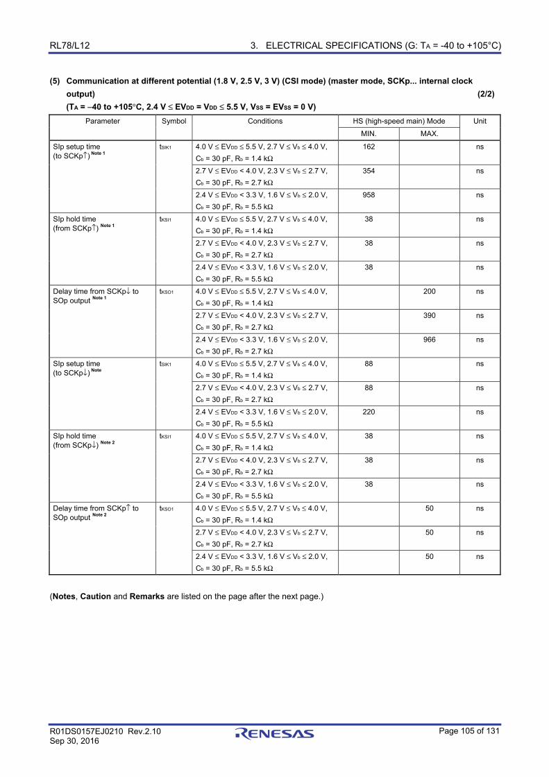
RL78/L12 3. ELECTRICAL SPECIFICATIONS (G: TA = -40 to +105°C)
R01DS0157EJ0210 Rev.2.10 Sep 30, 2016
Page 105 of 131
(5) Communication at different potential (1.8 V, 2.5 V, 3 V) (CSI mode) (master mode, SCKp... internal clock output) (2/2)
(TA = −40 to +105°C, 2.4 V ≤ EVDD = VDD ≤ 5.5 V, VSS = EVSS = 0 V) Parameter Symbol Conditions HS (high-speed main) Mode Unit
MIN. MAX.
SIp setup time (to SCKp↑) Note 1
tSIK1 4.0 V ≤ EVDD ≤ 5.5 V, 2.7 V ≤ Vb ≤ 4.0 V,
Cb = 30 pF, Rb = 1.4 kΩ
162 ns
2.7 V ≤ EVDD < 4.0 V, 2.3 V ≤ Vb ≤ 2.7 V,
Cb = 30 pF, Rb = 2.7 kΩ
354 ns
2.4 V ≤ EVDD < 3.3 V, 1.6 V ≤ Vb ≤ 2.0 V,
Cb = 30 pF, Rb = 5.5 kΩ
958 ns
SIp hold time (from SCKp↑) Note 1
tKSI1 4.0 V ≤ EVDD ≤ 5.5 V, 2.7 V ≤ Vb ≤ 4.0 V,
Cb = 30 pF, Rb = 1.4 kΩ
38 ns
2.7 V ≤ EVDD < 4.0 V, 2.3 V ≤ Vb ≤ 2.7 V,
Cb = 30 pF, Rb = 2.7 kΩ
38 ns
2.4 V ≤ EVDD < 3.3 V, 1.6 V ≤ Vb ≤ 2.0 V,
Cb = 30 pF, Rb = 5.5 kΩ
38 ns
Delay time from SCKp↓ to SOp output Note 1
tKSO1 4.0 V ≤ EVDD ≤ 5.5 V, 2.7 V ≤ Vb ≤ 4.0 V,
Cb = 30 pF, Rb = 1.4 kΩ
200 ns
2.7 V ≤ EVDD < 4.0 V, 2.3 V ≤ Vb ≤ 2.7 V,
Cb = 30 pF, Rb = 2.7 kΩ
390 ns
2.4 V ≤ EVDD < 3.3 V, 1.6 V ≤ Vb ≤ 2.0 V,
Cb = 30 pF, Rb = 2.7 kΩ
966 ns
SIp setup time (to SCKp↓) Note
tSIK1 4.0 V ≤ EVDD ≤ 5.5 V, 2.7 V ≤ Vb ≤ 4.0 V,
Cb = 30 pF, Rb = 1.4 kΩ
88 ns
2.7 V ≤ EVDD < 4.0 V, 2.3 V ≤ Vb ≤ 2.7 V,
Cb = 30 pF, Rb = 2.7 kΩ
88 ns
2.4 V ≤ EVDD < 3.3 V, 1.6 V ≤ Vb ≤ 2.0 V,
Cb = 30 pF, Rb = 5.5 kΩ
220 ns
SIp hold time (from SCKp↓) Note 2
tKSI1 4.0 V ≤ EVDD ≤ 5.5 V, 2.7 V ≤ Vb ≤ 4.0 V,
Cb = 30 pF, Rb = 1.4 kΩ
38 ns
2.7 V ≤ EVDD < 4.0 V, 2.3 V ≤ Vb ≤ 2.7 V,
Cb = 30 pF, Rb = 2.7 kΩ
38 ns
2.4 V ≤ EVDD < 3.3 V, 1.6 V ≤ Vb ≤ 2.0 V,
Cb = 30 pF, Rb = 5.5 kΩ
38 ns
Delay time from SCKp↑ to SOp output Note 2
tKSO1 4.0 V ≤ EVDD ≤ 5.5 V, 2.7 V ≤ Vb ≤ 4.0 V,
Cb = 30 pF, Rb = 1.4 kΩ
50 ns
2.7 V ≤ EVDD < 4.0 V, 2.3 V ≤ Vb ≤ 2.7 V,
Cb = 30 pF, Rb = 2.7 kΩ
50 ns
2.4 V ≤ EVDD < 3.3 V, 1.6 V ≤ Vb ≤ 2.0 V,
Cb = 30 pF, Rb = 5.5 kΩ
50 ns
(Notes, Caution and Remarks are listed on the page after the next page.)
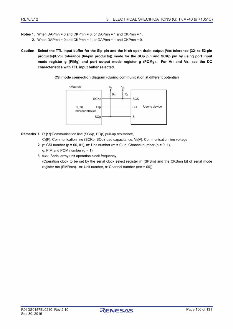
RL78/L12 3. ELECTRICAL SPECIFICATIONS (G: TA = -40 to +105°C)
R01DS0157EJ0210 Rev.2.10 Sep 30, 2016
Page 106 of 131
Notes 1. When DAPmn = 0 and CKPmn = 0, or DAPmn = 1 and CKPmn = 1.
2. When DAPmn = 0 and CKPmn = 1, or DAPmn = 1 and CKPmn = 0.
Caution Select the TTL input buffer for the SIp pin and the N-ch open drain output (VDD tolerance (32- to 52-pin products)/EVDD tolerance (64-pin products)) mode for the SOp pin and SCKp pin by using port input mode register g (PIMg) and port output mode register g (POMg). For VIH and VIL, see the DC characteristics with TTL input buffer selected.
CSI mode connection diagram (during communication at different potential)
Vb
Rb
SCKp
SOp
SCK
SI
SIp SO
Vb
Rb
<Master>
RL78microcontroller
User's device
Remarks 1. Rb[Ω]:Communication line (SCKp, SOp) pull-up resistance,
Cb[F]: Communication line (SCKp, SOp) load capacitance, Vb[V]: Communication line voltage
2. p: CSI number (p = 00, 01), m: Unit number (m = 0), n: Channel number (n = 0, 1),
g: PIM and POM number (g = 1)
3. fMCK: Serial array unit operation clock frequency
(Operation clock to be set by the serial clock select register m (SPSm) and the CKSmn bit of serial mode
register mn (SMRmn). m: Unit number, n: Channel number (mn = 00))
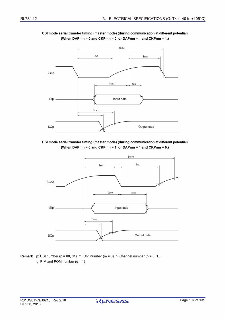
RL78/L12 3. ELECTRICAL SPECIFICATIONS (G: TA = -40 to +105°C)
R01DS0157EJ0210 Rev.2.10 Sep 30, 2016
Page 107 of 131
CSI mode serial transfer timing (master mode) (during communication at different potential) (When DAPmn = 0 and CKPmn = 0, or DAPmn = 1 and CKPmn = 1.)
SIp Input data
Output dataSOp
tKCY1
tKL1 tKH1
tSIK1 tKSI1
tKSO1
SCKp
CSI mode serial transfer timing (master mode) (during communication at different potential) (When DAPmn = 0 and CKPmn = 1, or DAPmn = 1 and CKPmn = 0.)
SIp Input data
Output dataSOp
tKCY1
tKL1tKH1
tSIK1 tKSI1
tKSO1
SCKp
Remark p: CSI number (p = 00, 01), m: Unit number (m = 0), n: Channel number (n = 0, 1),
g: PIM and POM number (g = 1)
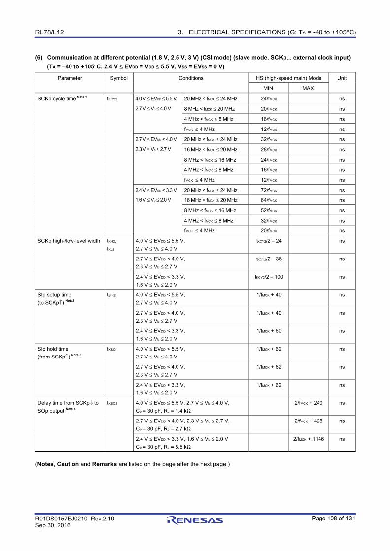
RL78/L12 3. ELECTRICAL SPECIFICATIONS (G: TA = -40 to +105°C)
R01DS0157EJ0210 Rev.2.10 Sep 30, 2016
Page 108 of 131
(6) Communication at different potential (1.8 V, 2.5 V, 3 V) (CSI mode) (slave mode, SCKp... external clock input) (TA = −40 to +105°C, 2.4 V ≤ EVDD = VDD ≤ 5.5 V, VSS = EVSS = 0 V)
Parameter Symbol Conditions HS (high-speed main) Mode Unit
MIN. MAX.
SCKp cycle time Note 1 tKCY2 4.0 V ≤ EVDD ≤ 5.5 V,
2.7 V ≤ Vb ≤ 4.0 V
20 MHz < fMCK ≤ 24 MHz 24/fMCK ns
8 MHz < fMCK ≤ 20 MHz 20/fMCK ns
4 MHz < fMCK ≤ 8 MHz 16/fMCK ns
fMCK ≤ 4 MHz 12/fMCK ns
2.7 V ≤ EVDD < 4.0 V,
2.3 V ≤ Vb ≤ 2.7 V
20 MHz < fMCK ≤ 24 MHz 32/fMCK ns
16 MHz < fMCK ≤ 20 MHz 28/fMCK ns
8 MHz < fMCK ≤ 16 MHz 24/fMCK ns
4 MHz < fMCK ≤ 8 MHz 16/fMCK ns
fMCK ≤ 4 MHz 12/fMCK ns
2.4 V ≤ EVDD < 3.3 V,
1.6 V ≤ Vb ≤ 2.0 V
20 MHz < fMCK ≤ 24 MHz 72/fMCK ns
16 MHz < fMCK ≤ 20 MHz 64/fMCK ns
8 MHz < fMCK ≤ 16 MHz 52/fMCK ns
4 MHz < fMCK ≤ 8 MHz 32/fMCK ns
fMCK ≤ 4 MHz 20/fMCK ns
SCKp high-/low-level width tKH2,
tKL2
4.0 V ≤ EVDD ≤ 5.5 V,
2.7 V ≤ Vb ≤ 4.0 V
tKCY2/2 − 24 ns
2.7 V ≤ EVDD < 4.0 V,
2.3 V ≤ Vb ≤ 2.7 V
tKCY2/2 − 36 ns
2.4 V ≤ EVDD < 3.3 V,
1.6 V ≤ Vb ≤ 2.0 V
tKCY2/2 − 100 ns
SIp setup time
(to SCKp↑) Note2
tSIK2 4.0 V ≤ EVDD < 5.5 V,
2.7 V ≤ Vb ≤ 4.0 V
1/fMCK + 40 ns
2.7 V ≤ EVDD < 4.0 V,
2.3 V ≤ Vb ≤ 2.7 V
1/fMCK + 40 ns
2.4 V ≤ EVDD < 3.3 V,
1.6 V ≤ Vb ≤ 2.0 V
1/fMCK + 60 ns
SIp hold time
(from SCKp↑) Note 3
tKSI2 4.0 V ≤ EVDD < 5.5 V,
2.7 V ≤ Vb ≤ 4.0 V
1/fMCK + 62 ns
2.7 V ≤ EVDD < 4.0 V,
2.3 V ≤ Vb ≤ 2.7 V
1/fMCK + 62 ns
2.4 V ≤ EVDD < 3.3 V,
1.6 V ≤ Vb ≤ 2.0 V
1/fMCK + 62 ns
Delay time from SCKp↓ to
SOp output Note 4
tKSO2 4.0 V ≤ EVDD ≤ 5.5 V, 2.7 V ≤ Vb ≤ 4.0 V,
Cb = 30 pF, Rb = 1.4 kΩ
2/fMCK + 240 ns
2.7 V ≤ EVDD < 4.0 V, 2.3 V ≤ Vb ≤ 2.7 V,
Cb = 30 pF, Rb = 2.7 kΩ
2/fMCK + 428 ns
2.4 V ≤ EVDD < 3.3 V, 1.6 V ≤ Vb ≤ 2.0 V
Cb = 30 pF, Rb = 5.5 kΩ
2/fMCK + 1146 ns
(Notes, Caution and Remarks are listed on the page after the next page.)
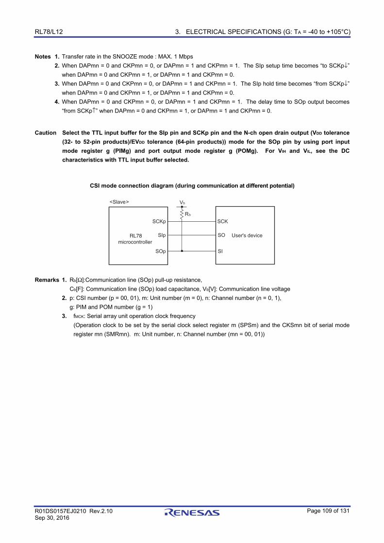
RL78/L12 3. ELECTRICAL SPECIFICATIONS (G: TA = -40 to +105°C)
R01DS0157EJ0210 Rev.2.10 Sep 30, 2016
Page 109 of 131
Notes 1. Transfer rate in the SNOOZE mode : MAX. 1 Mbps
2. When DAPmn = 0 and CKPmn = 0, or DAPmn = 1 and CKPmn = 1. The SIp setup time becomes “to SCKp↓”
when DAPmn = 0 and CKPmn = 1, or DAPmn = 1 and CKPmn = 0.
3. When DAPmn = 0 and CKPmn = 0, or DAPmn = 1 and CKPmn = 1. The SIp hold time becomes “from SCKp↓”
when DAPmn = 0 and CKPmn = 1, or DAPmn = 1 and CKPmn = 0.
4. When DAPmn = 0 and CKPmn = 0, or DAPmn = 1 and CKPmn = 1. The delay time to SOp output becomes
“from SCKp↑” when DAPmn = 0 and CKPmn = 1, or DAPmn = 1 and CKPmn = 0.
Caution Select the TTL input buffer for the SIp pin and SCKp pin and the N-ch open drain output (VDD tolerance (32- to 52-pin products)/EVDD tolerance (64-pin products)) mode for the SOp pin by using port input mode register g (PIMg) and port output mode register g (POMg). For VIH and VIL, see the DC characteristics with TTL input buffer selected.
CSI mode connection diagram (during communication at different potential)
User's device
<Slave>
SCKp
SOp
SCK
SI
SIp SO
Vb
Rb
RL78microcontroller
Remarks 1. Rb[Ω]:Communication line (SOp) pull-up resistance,
Cb[F]: Communication line (SOp) load capacitance, Vb[V]: Communication line voltage
2. p: CSI number (p = 00, 01), m: Unit number (m = 0), n: Channel number (n = 0, 1),
g: PIM and POM number (g = 1)
3. fMCK: Serial array unit operation clock frequency
(Operation clock to be set by the serial clock select register m (SPSm) and the CKSmn bit of serial mode
register mn (SMRmn). m: Unit number, n: Channel number (mn = 00, 01))
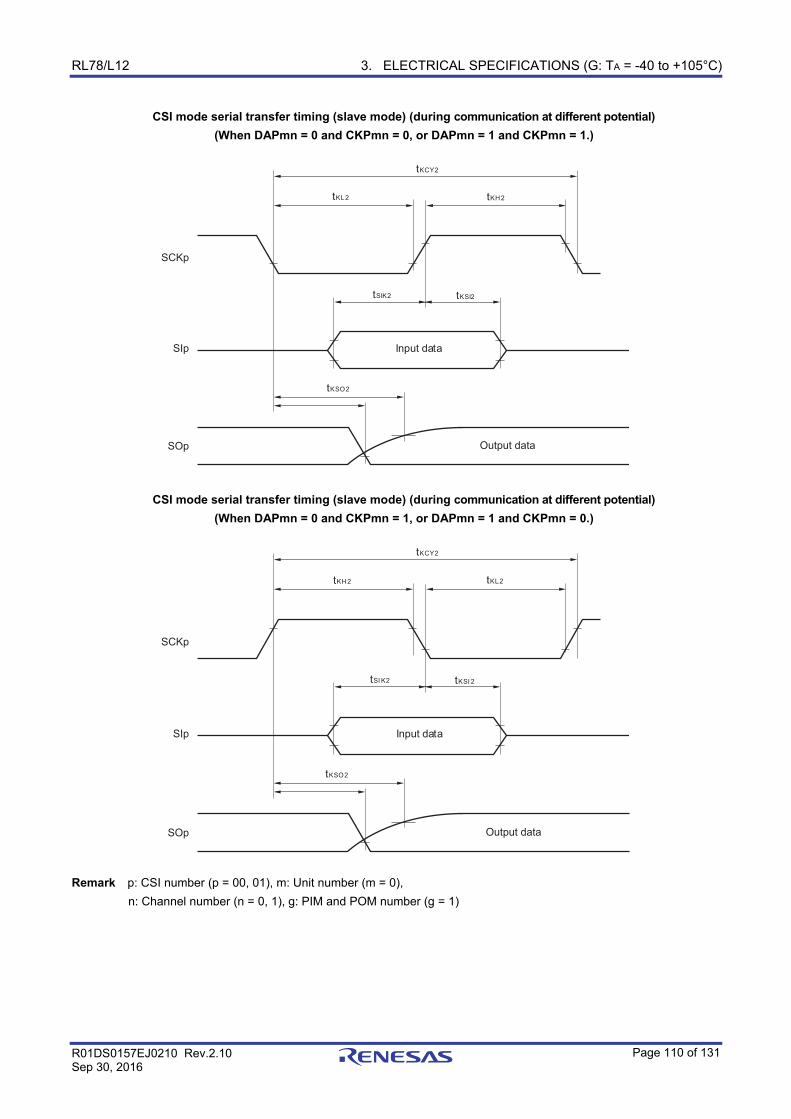
RL78/L12 3. ELECTRICAL SPECIFICATIONS (G: TA = -40 to +105°C)
R01DS0157EJ0210 Rev.2.10 Sep 30, 2016
Page 110 of 131
CSI mode serial transfer timing (slave mode) (during communication at different potential) (When DAPmn = 0 and CKPmn = 0, or DAPmn = 1 and CKPmn = 1.)
SIp Input data
Output dataSOp
tKCY2
tKL2 tKH2
tSIK2 tKSI2
tKSO2
SCKp
CSI mode serial transfer timing (slave mode) (during communication at different potential) (When DAPmn = 0 and CKPmn = 1, or DAPmn = 1 and CKPmn = 0.)
SIp Input data
Output dataSOp
tKCY2
tKL2tKH2
tSI K2 tKSI 2
tKSO2
SCKp
Remark p: CSI number (p = 00, 01), m: Unit number (m = 0),
n: Channel number (n = 0, 1), g: PIM and POM number (g = 1)
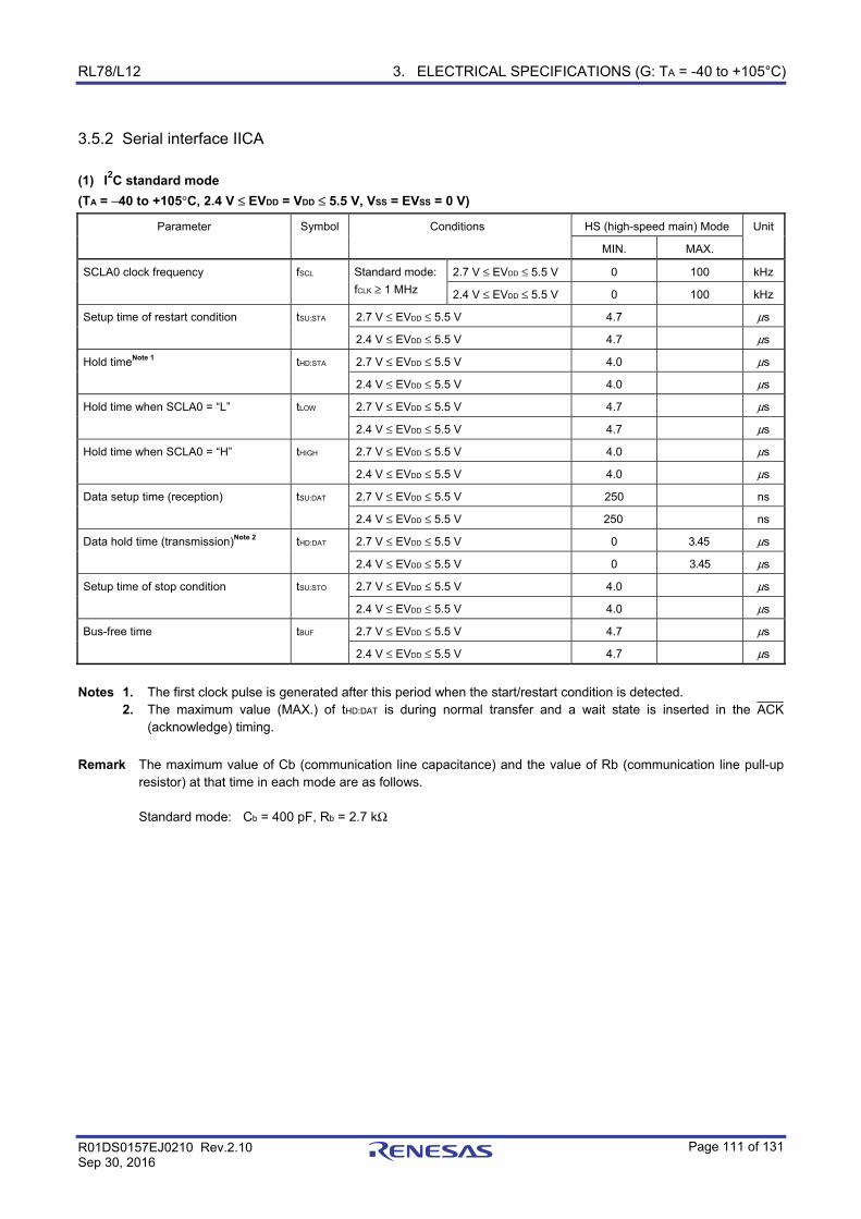
RL78/L12 3. ELECTRICAL SPECIFICATIONS (G: TA = -40 to +105°C)
R01DS0157EJ0210 Rev.2.10 Sep 30, 2016
Page 111 of 131
3.5.2 Serial interface IICA (1) I2C standard mode (TA = −40 to +105°C, 2.4 V ≤ EVDD = VDD ≤ 5.5 V, VSS = EVSS = 0 V)
Parameter Symbol Conditions HS (high-speed main) Mode Unit
MIN. MAX.
SCLA0 clock frequency fSCL Standard mode:
fCLK ≥ 1 MHz
2.7 V ≤ EVDD ≤ 5.5 V 0 100 kHz
2.4 V ≤ EVDD ≤ 5.5 V 0 100 kHz
Setup time of restart condition tSU:STA 2.7 V ≤ EVDD ≤ 5.5 V 4.7 μs
2.4 V ≤ EVDD ≤ 5.5 V 4.7 μs
Hold timeNote 1 tHD:STA 2.7 V ≤ EVDD ≤ 5.5 V 4.0 μs
2.4 V ≤ EVDD ≤ 5.5 V 4.0 μs
Hold time when SCLA0 = “L” tLOW 2.7 V ≤ EVDD ≤ 5.5 V 4.7 μs
2.4 V ≤ EVDD ≤ 5.5 V 4.7 μs
Hold time when SCLA0 = “H” tHIGH 2.7 V ≤ EVDD ≤ 5.5 V 4.0 μs
2.4 V ≤ EVDD ≤ 5.5 V 4.0 μs
Data setup time (reception) tSU:DAT 2.7 V ≤ EVDD ≤ 5.5 V 250 ns
2.4 V ≤ EVDD ≤ 5.5 V 250 ns
Data hold time (transmission)Note 2 tHD:DAT 2.7 V ≤ EVDD ≤ 5.5 V 0 3.45 μs
2.4 V ≤ EVDD ≤ 5.5 V 0 3.45 μs
Setup time of stop condition tSU:STO 2.7 V ≤ EVDD ≤ 5.5 V 4.0 μs
2.4 V ≤ EVDD ≤ 5.5 V 4.0 μs
Bus-free time tBUF 2.7 V ≤ EVDD ≤ 5.5 V 4.7 μs
2.4 V ≤ EVDD ≤ 5.5 V 4.7 μs
Notes 1. The first clock pulse is generated after this period when the start/restart condition is detected. 2. The maximum value (MAX.) of tHD:DAT is during normal transfer and a wait state is inserted in the ACK
(acknowledge) timing.
Remark The maximum value of Cb (communication line capacitance) and the value of Rb (communication line pull-up
resistor) at that time in each mode are as follows. Standard mode: Cb = 400 pF, Rb = 2.7 kΩ
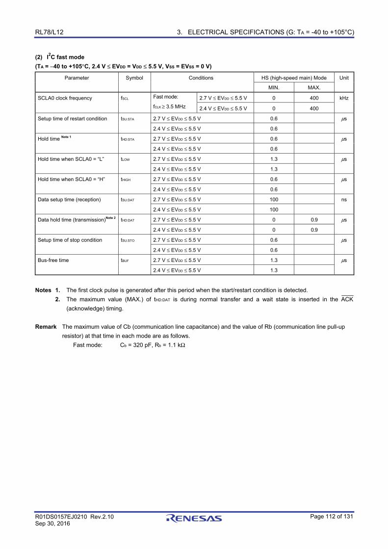
RL78/L12 3. ELECTRICAL SPECIFICATIONS (G: TA = -40 to +105°C)
R01DS0157EJ0210 Rev.2.10 Sep 30, 2016
Page 112 of 131
(2) I2C fast mode (TA = −40 to +105°C, 2.4 V ≤ EVDD = VDD ≤ 5.5 V, VSS = EVSS = 0 V)
Parameter Symbol Conditions HS (high-speed main) Mode Unit
MIN. MAX.
SCLA0 clock frequency fSCL Fast mode:
fCLK ≥ 3.5 MHz
2.7 V ≤ EVDD ≤ 5.5 V 0 400 kHz
2.4 V ≤ EVDD ≤ 5.5 V 0 400
Setup time of restart condition tSU:STA 2.7 V ≤ EVDD ≤ 5.5 V 0.6 μs
2.4 V ≤ EVDD ≤ 5.5 V 0.6
Hold time Note 1 tHD:STA 2.7 V ≤ EVDD ≤ 5.5 V 0.6 μs
2.4 V ≤ EVDD ≤ 5.5 V 0.6
Hold time when SCLA0 = “L” tLOW 2.7 V ≤ EVDD ≤ 5.5 V 1.3 μs
2.4 V ≤ EVDD ≤ 5.5 V 1.3
Hold time when SCLA0 = “H” tHIGH 2.7 V ≤ EVDD ≤ 5.5 V 0.6 μs
2.4 V ≤ EVDD ≤ 5.5 V 0.6
Data setup time (reception) tSU:DAT 2.7 V ≤ EVDD ≤ 5.5 V 100 ns
2.4 V ≤ EVDD ≤ 5.5 V 100
Data hold time (transmission)Note 2 tHD:DAT 2.7 V ≤ EVDD ≤ 5.5 V 0 0.9 μs
2.4 V ≤ EVDD ≤ 5.5 V 0 0.9
Setup time of stop condition tSU:STO 2.7 V ≤ EVDD ≤ 5.5 V 0.6 μs
2.4 V ≤ EVDD ≤ 5.5 V 0.6
Bus-free time tBUF 2.7 V ≤ EVDD ≤ 5.5 V 1.3 μs
2.4 V ≤ EVDD ≤ 5.5 V 1.3
Notes 1. The first clock pulse is generated after this period when the start/restart condition is detected.
2. The maximum value (MAX.) of tHD:DAT is during normal transfer and a wait state is inserted in the ACK
(acknowledge) timing.
Remark The maximum value of Cb (communication line capacitance) and the value of Rb (communication line pull-up
resistor) at that time in each mode are as follows.
Fast mode: Cb = 320 pF, Rb = 1.1 kΩ
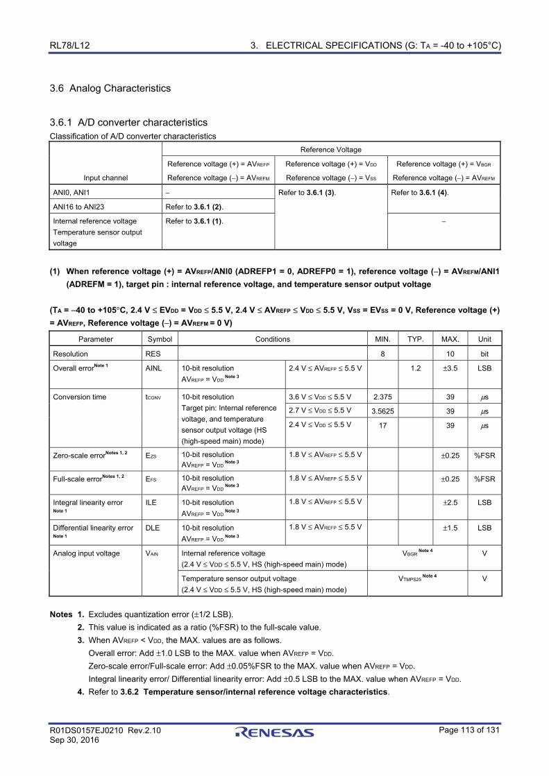
RL78/L12 3. ELECTRICAL SPECIFICATIONS (G: TA = -40 to +105°C)
R01DS0157EJ0210 Rev.2.10 Sep 30, 2016
Page 113 of 131
3.6 Analog Characteristics
3.6.1 A/D converter characteristics Classification of A/D converter characteristics
Input channel
Reference Voltage
Reference voltage (+) = AVREFP
Reference voltage (−) = AVREFM
Reference voltage (+) = VDD
Reference voltage (−) = VSS
Reference voltage (+) = VBGR
Reference voltage (−) = AVREFM
ANI0, ANI1 − Refer to 3.6.1 (3). Refer to 3.6.1 (4).
ANI16 to ANI23 Refer to 3.6.1 (2).
Internal reference voltage
Temperature sensor output
voltage
Refer to 3.6.1 (1). −
(1) When reference voltage (+) = AVREFP/ANI0 (ADREFP1 = 0, ADREFP0 = 1), reference voltage (−) = AVREFM/ANI1
(ADREFM = 1), target pin : internal reference voltage, and temperature sensor output voltage (TA = −40 to +105°C, 2.4 V ≤ EVDD = VDD ≤ 5.5 V, 2.4 V ≤ AVREFP ≤ VDD ≤ 5.5 V, VSS = EVSS = 0 V, Reference voltage (+) = AVREFP, Reference voltage (−) = AVREFM = 0 V)
Parameter Symbol Conditions MIN. TYP. MAX. Unit
Resolution RES 8 10 bit
Overall errorNote 1 AINL 10-bit resolution
AVREFP = VDD Note 3
2.4 V ≤ AVREFP ≤ 5.5 V 1.2 ±3.5 LSB
Conversion time tCONV 10-bit resolution
Target pin: Internal reference
voltage, and temperature
sensor output voltage (HS
(high-speed main) mode)
3.6 V ≤ VDD ≤ 5.5 V 2.375 39 μs
2.7 V ≤ VDD ≤ 5.5 V 3.5625 39 μs
2.4 V ≤ VDD ≤ 5.5 V 17 39 μs
Zero-scale errorNotes 1, 2 EZS 10-bit resolution AVREFP = VDD
Note 3 1.8 V ≤ AVREFP ≤ 5.5 V ±0.25 %FSR
Full-scale errorNotes 1, 2 EFS 10-bit resolution AVREFP = VDD
Note 3 1.8 V ≤ AVREFP ≤ 5.5 V ±0.25 %FSR
Integral linearity error Note 1
ILE 10-bit resolution
AVREFP = VDD Note 3
1.8 V ≤ AVREFP ≤ 5.5 V ±2.5 LSB
Differential linearity error
Note 1
DLE 10-bit resolution
AVREFP = VDD Note 3
1.8 V ≤ AVREFP ≤ 5.5 V ±1.5 LSB
Analog input voltage VAIN Internal reference voltage
(2.4 V ≤ VDD ≤ 5.5 V, HS (high-speed main) mode)
VBGR Note 4 V
Temperature sensor output voltage
(2.4 V ≤ VDD ≤ 5.5 V, HS (high-speed main) mode)
VTMPS25 Note 4 V
Notes 1. Excludes quantization error (±1/2 LSB).
2. This value is indicated as a ratio (%FSR) to the full-scale value.
3. When AVREFP < VDD, the MAX. values are as follows.
Overall error: Add ±1.0 LSB to the MAX. value when AVREFP = VDD.
Zero-scale error/Full-scale error: Add ±0.05%FSR to the MAX. value when AVREFP = VDD.
Integral linearity error/ Differential linearity error: Add ±0.5 LSB to the MAX. value when AVREFP = VDD.
4. Refer to 3.6.2 Temperature sensor/internal reference voltage characteristics.
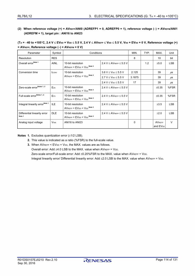
RL78/L12 3. ELECTRICAL SPECIFICATIONS (G: TA = -40 to +105°C)
R01DS0157EJ0210 Rev.2.10 Sep 30, 2016
Page 114 of 131
(2) When reference voltage (+) = AVREFP/ANI0 (ADREFP1 = 0, ADREFP0 = 1), reference voltage (−) = AVREFM/ANI1 (ADREFM = 1), target pin : ANI16 to ANI23
(TA = −40 to +105°C, 2.4 V ≤ EVDD = VDD ≤ 5.5 V, 2.4 V ≤ AVREFP ≤ VDD ≤ 5.5 V, VSS = EVSS = 0 V, Reference voltage (+) = AVREFP, Reference voltage (−) = AVREFM = 0 V)
Parameter Symbol Conditions MIN. TYP. MAX. Unit
Resolution RES 8 10 bit
Overall errorNote 1 AINL 10-bit resolution
AVREFP = EVDD = VDD Note 3
2.4 V ≤ AVREFP ≤ 5.5 V 1.2 ±5.0 LSB
Conversion time tCONV 10-bit resolution
AVREFP = EVDD = VDD Note 3
3.6 V ≤ VDD ≤ 5.5 V 2.125 39 μs
2.7 V ≤ VDD ≤ 5.5 V 3.1875 39 μs
2.4 V ≤ VDD ≤ 5.5 V 17 39 μs
Zero-scale errorNotes 1, 2 EZS 10-bit resolution AVREFP = EVDD = VDD
Note 3 2.4 V ≤ AVREFP ≤ 5.5 V ±0.35 %FSR
Full-scale errorNotes 1, 2 EFS 10-bit resolution AVREFP = EVDD = VDD
Note 3 2.4 V ≤ AVREFP ≤ 5.5 V ±0.35 %FSR
Integral linearity errorNote 1 ILE 10-bit resolution
AVREFP = EVDD = VDD Note 3
2.4 V ≤ AVREFP ≤ 5.5 V ±3.5 LSB
Differential linearity error
Note 1
DLE 10-bit resolution
AVREFP = EVDD = VDD Note 3
2.4 V ≤ AVREFP ≤ 5.5 V ±2.0 LSB
Analog input voltage VAIN ANI16 to ANI23 0 AVREFP
and EVDD
V
Notes 1. Excludes quantization error (±1/2 LSB).
2. This value is indicated as a ratio (%FSR) to the full-scale value.
3. When AVREFP < EVDD = VDD, the MAX. values are as follows.
Overall error: Add ±4.0 LSB to the MAX. value when AVREFP = VDD.
Zero-scale error/Full-scale error: Add ±0.20%FSR to the MAX. value when AVREFP = VDD.
Integral linearity error/ Differential linearity error: Add ±2.0 LSB to the MAX. value when AVREFP = VDD.
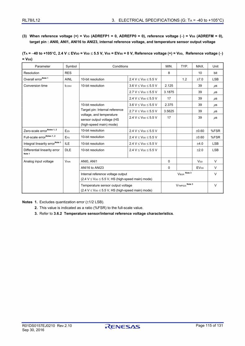
RL78/L12 3. ELECTRICAL SPECIFICATIONS (G: TA = -40 to +105°C)
R01DS0157EJ0210 Rev.2.10 Sep 30, 2016
Page 115 of 131
(3) When reference voltage (+) = VDD (ADREFP1 = 0, ADREFP0 = 0), reference voltage (−) = VSS (ADREFM = 0), target pin : ANI0, ANI1, ANI16 to ANI23, internal reference voltage, and temperature sensor output voltage
(TA = −40 to +105°C, 2.4 V ≤ EVDD = VDD ≤ 5.5 V, VSS = EVSS = 0 V, Reference voltage (+) = VDD, Reference voltage (−) = VSS)
Parameter Symbol Conditions MIN. TYP. MAX. Unit
Resolution RES 8 10 bit
Overall errorNote 1 AINL 10-bit resolution 2.4 V ≤ VDD ≤ 5.5 V 1.2 ±7.0 LSB
Conversion time tCONV 10-bit resolution 3.6 V ≤ VDD ≤ 5.5 V 2.125 39 μs
2.7 V ≤ VDD ≤ 5.5 V 3.1875 39 μs
2.4 V ≤ VDD ≤ 5.5 V 17 39 μs
10-bit resolution
Target pin: Internal reference
voltage, and temperature
sensor output voltage (HS
(high-speed main) mode)
3.6 V ≤ VDD ≤ 5.5 V 2.375 39 μs
2.7 V ≤ VDD ≤ 5.5 V 3.5625 39 μs
2.4 V ≤ VDD ≤ 5.5 V 17 39 μs
Zero-scale errorNotes 1, 2 EZS 10-bit resolution 2.4 V ≤ VDD ≤ 5.5 V ±0.60 %FSR
Full-scale errorNotes 1, 2 EFS 10-bit resolution 2.4 V ≤ VDD ≤ 5.5 V ±0.60 %FSR
Integral linearity errorNote 1 ILE 10-bit resolution 2.4 V ≤ VDD ≤ 5.5 V ±4.0 LSB
Differential linearity error
Note 1
DLE 10-bit resolution 2.4 V ≤ VDD ≤ 5.5 V ±2.0 LSB
Analog input voltage VAIN ANI0, ANI1 0 VDD V
ANI16 to ANI23 0 EVDD V
Internal reference voltage output
(2.4 V ≤ VDD ≤ 5.5 V, HS (high-speed main) mode)
VBGR Note 3 V
Temperature sensor output voltage
(2.4 V ≤ VDD ≤ 5.5 V, HS (high-speed main) mode)
VTMPS25 Note 3 V
Notes 1. Excludes quantization error (±1/2 LSB).
2. This value is indicated as a ratio (%FSR) to the full-scale value.
3. Refer to 3.6.2 Temperature sensor/internal reference voltage characteristics.
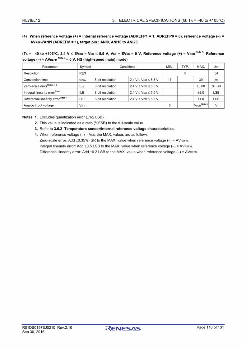
RL78/L12 3. ELECTRICAL SPECIFICATIONS (G: TA = -40 to +105°C)
R01DS0157EJ0210 Rev.2.10 Sep 30, 2016
Page 116 of 131
(4) When reference voltage (+) = Internal reference voltage (ADREFP1 = 1, ADREFP0 = 0), reference voltage (−) = AVREFM/ANI1 (ADREFM = 1), target pin : ANI0, ANI16 to ANI23
(TA = −40 to +105°C, 2.4 V ≤ EVDD = VDD ≤ 5.5 V, VSS = EVSS = 0 V, Reference voltage (+) = VBGR
Note 3, Reference voltage (−) = AVREFM
Note 4 = 0 V, HS (high-speed main) mode)
Parameter Symbol Conditions MIN. TYP. MAX. Unit
Resolution RES 8 bit
Conversion time tCONV 8-bit resolution 2.4 V ≤ VDD ≤ 5.5 V 17 39 μs
Zero-scale errorNotes 1, 2 EZS 8-bit resolution 2.4 V ≤ VDD ≤ 5.5 V ±0.60 %FSR
Integral linearity errorNote 1 ILE 8-bit resolution 2.4 V ≤ VDD ≤ 5.5 V ±2.0 LSB
Differential linearity error Note 1 DLE 8-bit resolution 2.4 V ≤ VDD ≤ 5.5 V ±1.0 LSB
Analog input voltage VAIN 0 VBGR Note 3 V
Notes 1. Excludes quantization error (±1/2 LSB).
2. This value is indicated as a ratio (%FSR) to the full-scale value.
3. Refer to 3.6.2 Temperature sensor/internal reference voltage characteristics.
4. When reference voltage (−) = VSS, the MAX. values are as follows.
Zero-scale error: Add ±0.35%FSR to the MAX. value when reference voltage (−) = AVREFM.
Integral linearity error: Add ±0.5 LSB to the MAX. value when reference voltage (−) = AVREFM.
Differential linearity error: Add ±0.2 LSB to the MAX. value when reference voltage (−) = AVREFM.
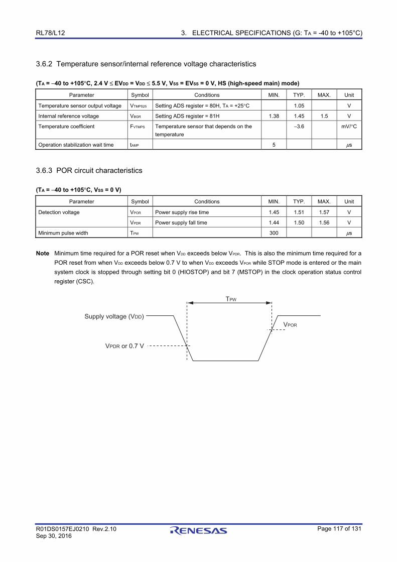
RL78/L12 3. ELECTRICAL SPECIFICATIONS (G: TA = -40 to +105°C)
R01DS0157EJ0210 Rev.2.10 Sep 30, 2016
Page 117 of 131
3.6.2 Temperature sensor/internal reference voltage characteristics
(TA = −40 to +105°C, 2.4 V ≤ EVDD = VDD ≤ 5.5 V, VSS = EVSS = 0 V, HS (high-speed main) mode)
Parameter Symbol Conditions MIN. TYP. MAX. Unit
Temperature sensor output voltage VTMPS25 Setting ADS register = 80H, TA = +25°C 1.05 V
Internal reference voltage VBGR Setting ADS register = 81H 1.38 1.45 1.5 V
Temperature coefficient FVTMPS Temperature sensor that depends on the
temperature
−3.6 mV/°C
Operation stabilization wait time tAMP 5 μs
3.6.3 POR circuit characteristics
(TA = −40 to +105°C, VSS = 0 V)
Parameter Symbol Conditions MIN. TYP. MAX. Unit
Detection voltage VPOR Power supply rise time 1.45 1.51 1.57 V
VPDR Power supply fall time 1.44 1.50 1.56 V
Minimum pulse width TPW 300 μs
Note Minimum time required for a POR reset when VDD exceeds below VPDR. This is also the minimum time required for a
POR reset from when VDD exceeds below 0.7 V to when VDD exceeds VPOR while STOP mode is entered or the main
system clock is stopped through setting bit 0 (HIOSTOP) and bit 7 (MSTOP) in the clock operation status control
register (CSC).
TPW
VPOR
VPDR or 0.7 V
Supply voltage (VDD)
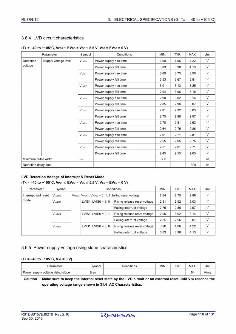
RL78/L12 3. ELECTRICAL SPECIFICATIONS (G: TA = -40 to +105°C)
R01DS0157EJ0210 Rev.2.10 Sep 30, 2016
Page 118 of 131
3.6.4 LVD circuit characteristics (TA = −40 to +105°C, VPDR ≤ EVDD = VDD ≤ 5.5 V, VSS = EVSS = 0 V)
Parameter Symbol Conditions MIN. TYP. MAX. Unit
Detection
voltage
Supply voltage level VLVD0 Power supply rise time 3.90 4.06 4.22 V
Power supply fall time 3.83 3.98 4.13 V
VLVD1 Power supply rise time 3.60 3.75 3.90 V
Power supply fall time 3.53 3.67 3.81 V
VLVD2 Power supply rise time 3.01 3.13 3.25 V
Power supply fall time 2.94 3.06 3.18 V
VLVD3 Power supply rise time 2.90 3.02 3.14 V
Power supply fall time 2.85 2.96 3.07 V
VLVD4 Power supply rise time 2.81 2.92 3.03 V
Power supply fall time 2.75 2.86 2.97 V
VLVD5 Power supply rise time 2.70 2.81 2.92 V
Power supply fall time 2.64 2.75 2.86 V
VLVD6 Power supply rise time 2.61 2.71 2.81 V
Power supply fall time 2.55 2.65 2.75 V
VLVD7 Power supply rise time 2.51 2.61 2.71 V
Power supply fall time 2.45 2.55 2.65 V
Minimum pulse width tLW 300 μs
Detection delay time 300 μs
LVD Detection Voltage of Interrupt & Reset Mode (TA = −40 to +105°C, VPDR ≤ EVDD = VDD ≤ 5.5 V, VSS = EVSS = 0 V)
Parameter Symbol Conditions MIN. TYP. MAX. Unit
Interrupt and reset
mode
VLVDD0 VPOC2, VPOC1, VPOC0 = 0, 1, 1, falling reset voltage 2.64 2.75 2.86 V
VLVDD1 LVIS1, LVIS0 = 1, 0 Rising release reset voltage 2.81 2.92 3.03 V
Falling interrupt voltage 2.75 2.86 2.97 V
VLVDD2 LVIS1, LVIS0 = 0, 1 Rising release reset voltage 2.90 3.02 3.14 V
Falling interrupt voltage 2.85 2.96 3.07 V
VLVDD3 LVIS1, LVIS0 = 0, 0 Rising release reset voltage 3.90 4.06 4.22 V
Falling interrupt voltage 3.83 3.98 4.13 V
3.6.5 Power supply voltage rising slope characteristics (TA = −40 to +105°C, VSS = 0 V)
Parameter Symbol Conditions MIN. TYP. MAX. Unit
Power supply voltage rising slope SVDD 54 V/ms
Caution Make sure to keep the internal reset state by the LVD circuit or an external reset until VDD reaches the operating voltage range shown in 31.4 AC Characteristics.
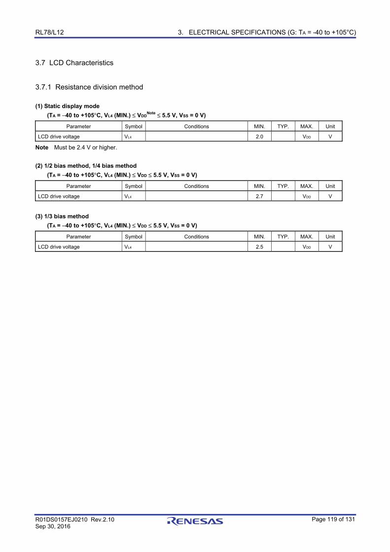
RL78/L12 3. ELECTRICAL SPECIFICATIONS (G: TA = -40 to +105°C)
R01DS0157EJ0210 Rev.2.10 Sep 30, 2016
Page 119 of 131
3.7 LCD Characteristics
3.7.1 Resistance division method (1) Static display mode
(TA = −40 to +105°C, VL4 (MIN.) ≤ VDDNote ≤ 5.5 V, VSS = 0 V)
Parameter Symbol Conditions MIN. TYP. MAX. Unit
LCD drive voltage VL4 2.0 VDD V
Note Must be 2.4 V or higher.
(2) 1/2 bias method, 1/4 bias method (TA = −40 to +105°C, VL4 (MIN.) ≤ VDD ≤ 5.5 V, VSS = 0 V)
Parameter Symbol Conditions MIN. TYP. MAX. Unit
LCD drive voltage VL4 2.7 VDD V
(3) 1/3 bias method
(TA = −40 to +105°C, VL4 (MIN.) ≤ VDD ≤ 5.5 V, VSS = 0 V)
Parameter Symbol Conditions MIN. TYP. MAX. Unit
LCD drive voltage VL4 2.5 VDD V
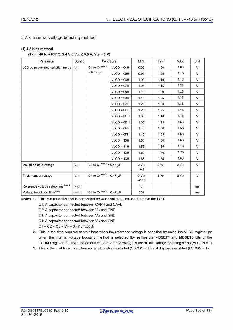
RL78/L12 3. ELECTRICAL SPECIFICATIONS (G: TA = -40 to +105°C)
R01DS0157EJ0210 Rev.2.10 Sep 30, 2016
Page 120 of 131
3.7.2 Internal voltage boosting method (1) 1/3 bias method
(TA = −40 to +105°C, 2.4 V ≤ VDD ≤ 5.5 V, VSS = 0 V)
Parameter Symbol Conditions MIN. TYP. MAX. Unit
LCD output voltage variation range VL1 C1 to C4Note 1
= 0.47 μF
VLCD = 04H 0.90 1.00 1.08 V
VLCD = 05H 0.95 1.05 1.13 V
VLCD = 06H 1.00 1.10 1.18 V
VLCD = 07H 1.05 1.15 1.23 V
VLCD = 08H 1.10 1.20 1.28 V
VLCD = 09H 1.15 1.25 1.33 V
VLCD = 0AH 1.20 1.30 1.38 V
VLCD = 0BH 1.25 1.35 1.43 V
VLCD = 0CH 1.30 1.40 1.48 V
VLCD = 0DH 1.35 1.45 1.53 V
VLCD = 0EH 1.40 1.50 1.58 V
VLCD = 0FH 1.45 1.55 1.63 V
VLCD = 10H 1.50 1.60 1.68 V
VLCD = 11H 1.55 1.65 1.73 V
VLCD = 12H 1.60 1.70 1.78 V
VLCD = 13H 1.65 1.75 1.83 V
Doubler output voltage VL2 C1 to C4Note 1 = 0.47 μF 2 VL1
−0.1
2 VL1 2 VL1 V
Tripler output voltage VL4 C1 to C4Note 1 = 0.47 μF 3 VL1
−0.15
3 VL1 3 VL1 V
Reference voltage setup time Note 2 tVWAIT1 5 ms
Voltage boost wait timeNote 3 tVWAIT2 C1 to C4Note 1 = 0.47 μF 500 ms
Notes 1. This is a capacitor that is connected between voltage pins used to drive the LCD.
C1: A capacitor connected between CAPH and CAPL
C2: A capacitor connected between VL1 and GND
C3: A capacitor connected between VL2 and GND
C4: A capacitor connected between VL4 and GND
C1 = C2 = C3 = C4 = 0.47 μF±30%
2. This is the time required to wait from when the reference voltage is specified by using the VLCD register (or
when the internal voltage boosting method is selected [by setting the MDSET1 and MDSET0 bits of the
LCDM0 register to 01B] if the default value reference voltage is used) until voltage boosting starts (VLCON = 1).
3. This is the wait time from when voltage boosting is started (VLCON = 1) until display is enabled (LCDON = 1).
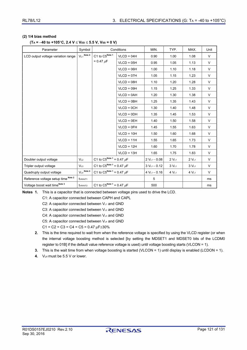
RL78/L12 3. ELECTRICAL SPECIFICATIONS (G: TA = -40 to +105°C)
R01DS0157EJ0210 Rev.2.10 Sep 30, 2016
Page 121 of 131
(2) 1/4 bias method (TA = −40 to +105°C, 2.4 V ≤ VDD ≤ 5.5 V, VSS = 0 V)
Parameter Symbol Conditions MIN. TYP. MAX. Unit
LCD output voltage variation range VL1 Note 4 C1 to C5Note 1
= 0.47 μF
VLCD = 04H 0.90 1.00 1.08 V
VLCD = 05H 0.95 1.05 1.13 V
VLCD = 06H 1.00 1.10 1.18 V
VLCD = 07H 1.05 1.15 1.23 V
VLCD = 08H 1.10 1.20 1.28 V
VLCD = 09H 1.15 1.25 1.33 V
VLCD = 0AH 1.20 1.30 1.38 V
VLCD = 0BH 1.25 1.35 1.43 V
VLCD = 0CH 1.30 1.40 1.48 V
VLCD = 0DH 1.35 1.45 1.53 V
VLCD = 0EH 1.40 1.50 1.58 V
VLCD = 0FH 1.45 1.55 1.63 V
VLCD = 10H 1.50 1.60 1.68 V
VLCD = 11H 1.55 1.65 1.73 V
VLCD = 12H 1.60 1.70 1.78 V
VLCD = 13H 1.65 1.75 1.83 V
Doubler output voltage VL2 C1 to C5Note 1 = 0.47 μF 2 VL1 − 0.08 2 VL1 2 VL1 V
Tripler output voltage VL3 C1 to C5Note 1 = 0.47 μF 3 VL1 − 0.12 3 VL1 3 VL1 V
Quadruply output voltage VL4 Note 4 C1 to C5Note 1 = 0.47 μF 4 VL1 − 0.16 4 VL1 4 VL1 V
Reference voltage setup time Note 2 tVWAIT1 5 ms
Voltage boost wait timeNote 3 tVWAIT2 C1 to C5Note 1 = 0.47 μF 500 ms
Notes 1. This is a capacitor that is connected between voltage pins used to drive the LCD.
C1: A capacitor connected between CAPH and CAPL
C2: A capacitor connected between VL1 and GND
C3: A capacitor connected between VL2 and GND
C4: A capacitor connected between VL3 and GND
C5: A capacitor connected between VL4 and GND
C1 = C2 = C3 = C4 = C5 = 0.47 μF±30%
2. This is the time required to wait from when the reference voltage is specified by using the VLCD register (or when
the internal voltage boosting method is selected [by setting the MDSET1 and MDSET0 bits of the LCDM0
register to 01B] if the default value reference voltage is used) until voltage boosting starts (VLCON = 1).
3. This is the wait time from when voltage boosting is started (VLCON = 1) until display is enabled (LCDON = 1).
4. VL4 must be 5.5 V or lower.
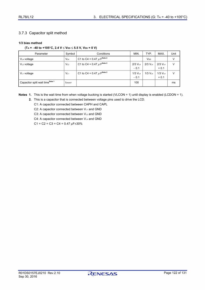
RL78/L12 3. ELECTRICAL SPECIFICATIONS (G: TA = -40 to +105°C)
R01DS0157EJ0210 Rev.2.10 Sep 30, 2016
Page 122 of 131
3.7.3 Capacitor split method 1/3 bias method
(TA = −40 to +105°C, 2.4 V ≤ VDD ≤ 5.5 V, VSS = 0 V)
Parameter Symbol Conditions MIN. TYP. MAX. Unit
VL4 voltage VL4 C1 to C4 = 0.47 μ FNote 2 VDD V
VL2 voltage VL2 C1 to C4 = 0.47 μ FNote 2 2/3 VL4
− 0.1
2/3 VL4 2/3 VL4
+ 0.1
V
VL1 voltage VL1 C1 to C4 = 0.47 μ FNote 2 1/3 VL4
− 0.1
1/3 VL4 1/3 VL4
+ 0.1
V
Capacitor split wait timeNote 1 tVWAIT 100 ms
Notes 1. This is the wait time from when voltage bucking is started (VLCON = 1) until display is enabled (LCDON = 1).
2. This is a capacitor that is connected between voltage pins used to drive the LCD.
C1: A capacitor connected between CAPH and CAPL
C2: A capacitor connected between VL1 and GND
C3: A capacitor connected between VL2 and GND
C4: A capacitor connected between VL4 and GND
C1 = C2 = C3 = C4 = 0.47 μF±30%
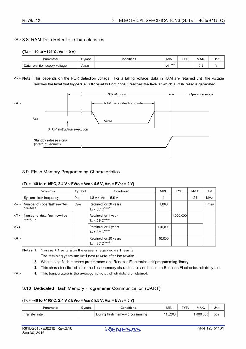
RL78/L12 3. ELECTRICAL SPECIFICATIONS (G: TA = -40 to +105°C)
R01DS0157EJ0210 Rev.2.10 Sep 30, 2016
Page 123 of 131
3.8 RAM Data Retention Characteristics (TA = −40 to +105°C, VSS = 0 V)
Parameter Symbol Conditions MIN. TYP. MAX. Unit
Data retention supply voltage VDDDR 1.44Note 5.5 V
Note This depends on the POR detection voltage. For a falling voltage, data in RAM are retained until the voltage
reaches the level that triggers a POR reset but not once it reaches the level at which a POR reset is generated.
VDD
STOP instruction execution
Standby release signal(interrupt request)
STOP mode
RAM Data retention mode
VDDDR
Operation mode
3.9 Flash Memory Programming Characteristics (TA = −40 to +105°C, 2.4 V ≤ EVDD = VDD ≤ 5.5 V, VSS = EVSS = 0 V)
Parameter Symbol Conditions MIN. TYP. MAX. Unit
System clock frequency fCLK 1.8 V ≤ VDD ≤ 5.5 V 1 24 MHz
Number of code flash rewrites Notes 1, 2, 3
Cerwr Retained for 20 years
TA = 85°CNote 4
1,000 Times
Number of data flash rewrites Notes 1, 2, 3
Retained for 1 year
TA = 25°CNote 4
1,000,000
Retained for 5 years
TA = 85°CNote 4
100,000
Retained for 20 years
TA = 85°CNote 4
10,000
Notes 1. 1 erase + 1 write after the erase is regarded as 1 rewrite.
The retaining years are until next rewrite after the rewrite.
2. When using flash memory programmer and Renesas Electronics self programming library
3. This characteristic indicates the flash memory characteristic and based on Renesas Electronics reliability test.
4. This temperature is the average value at which data are retained.
3.10 Dedicated Flash Memory Programmer Communication (UART) (TA = −40 to +105°C, 2.4 V ≤ EVDD = VDD ≤ 5.5 V, VSS = EVSS = 0 V)
Parameter Symbol Conditions MIN. TYP. MAX. Unit
Transfer rate During flash memory programming 115,200 1,000,000 bps
<R>
<R>
<R>
<R>
<R>
<R>
<R>
<R>
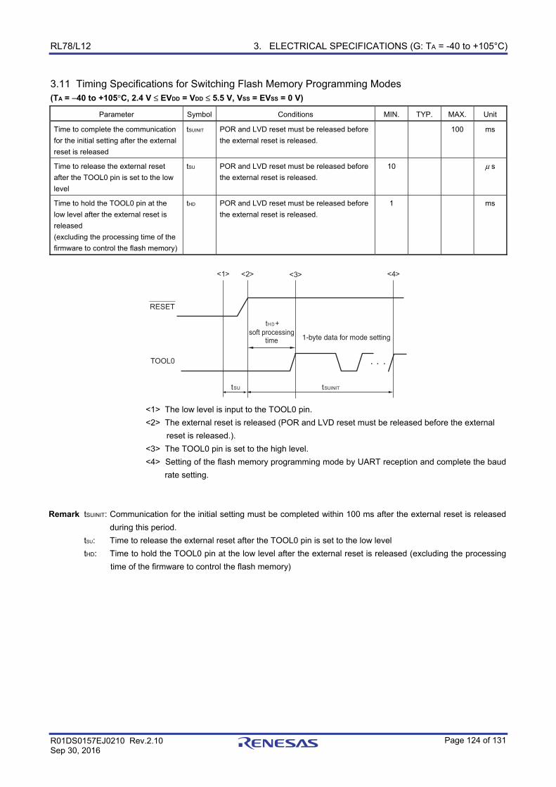
RL78/L12 3. ELECTRICAL SPECIFICATIONS (G: TA = -40 to +105°C)
R01DS0157EJ0210 Rev.2.10 Sep 30, 2016
Page 124 of 131
3.11 Timing Specifications for Switching Flash Memory Programming Modes (TA = −40 to +105°C, 2.4 V ≤ EVDD = VDD ≤ 5.5 V, VSS = EVSS = 0 V)
Parameter Symbol Conditions MIN. TYP. MAX. Unit
Time to complete the communication
for the initial setting after the external
reset is released
tSUINIT POR and LVD reset must be released before
the external reset is released.
100 ms
Time to release the external reset
after the TOOL0 pin is set to the low
level
tSU POR and LVD reset must be released before
the external reset is released.
10 μ s
Time to hold the TOOL0 pin at the
low level after the external reset is
released
(excluding the processing time of the
firmware to control the flash memory)
tHD POR and LVD reset must be released before
the external reset is released.
1 ms
RESET
TOOL0
<1> <2> <3>
tSUINIT
tH D+
soft processingtime
tSU
<4>
1-byte data for mode setting
<1> The low level is input to the TOOL0 pin.
<2> The external reset is released (POR and LVD reset must be released before the external
reset is released.).
<3> The TOOL0 pin is set to the high level.
<4> Setting of the flash memory programming mode by UART reception and complete the baud
rate setting.
Remark tSUINIT: Communication for the initial setting must be completed within 100 ms after the external reset is released
during this period.
tSU: Time to release the external reset after the TOOL0 pin is set to the low level
tHD: Time to hold the TOOL0 pin at the low level after the external reset is released (excluding the processing
time of the firmware to control the flash memory)
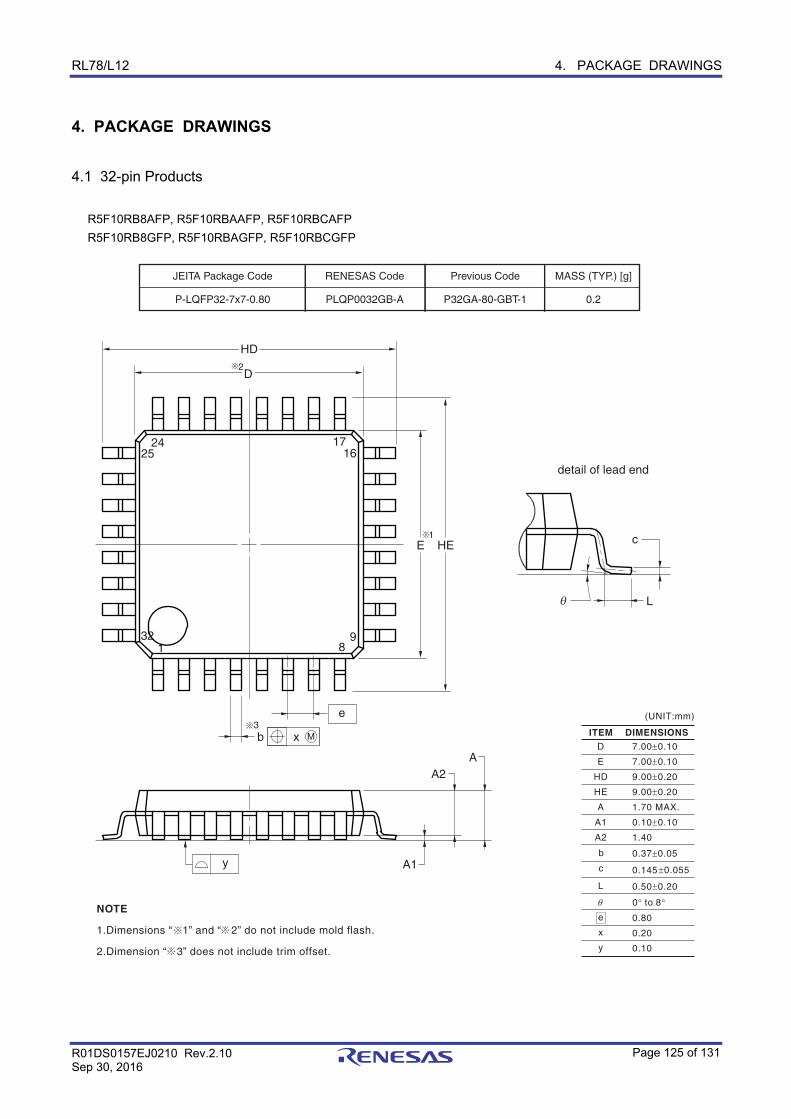
RL78/L12 4. PACKAGE DRAWINGS
R01DS0157EJ0210 Rev.2.10 Sep 30, 2016
Page 125 of 131
4. PACKAGE DRAWINGS
4.1 32-pin Products
R5F10RB8AFP, R5F10RBAAFP, R5F10RBCAFP
R5F10RB8GFP, R5F10RBAGFP, R5F10RBCGFP
0.145±0.055
(UNIT:mm)
ITEM DIMENSIONS
D
E
HD
HE
A
A1
A2
7.00±0.10
7.00±0.10
9.00±0.20
9.00±0.20
1.70 MAX.
0.10±0.10
1.40
c
θ
e
x
y
0.80
0.20
0.10
L 0.50±0.20
0° to 8°
0.37±0.05b
NOTE
1.Dimensions “ 1” and “ 2” do not include mold flash.
2.Dimension “ 3” does not include trim offset.
y
e
xb M
θ L
c
HD
HE
A1
A2A
D
E
detail of lead end
8
16
132 9
1725
24
2
1
3
JEITA Package Code RENESAS Code Previous Code MASS (TYP.) [g]
P-LQFP32-7x7-0.80 PLQP0032GB-A P32GA-80-GBT-1 0.2
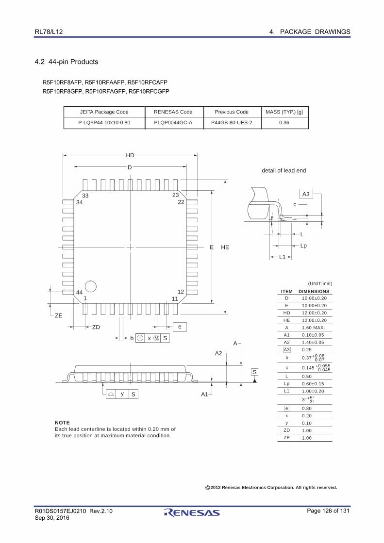
RL78/L12 4. PACKAGE DRAWINGS
R01DS0157EJ0210 Rev.2.10 Sep 30, 2016
Page 126 of 131
4.2 44-pin Products
R5F10RF8AFP, R5F10RFAAFP, R5F10RFCAFP
R5F10RF8GFP, R5F10RFAGFP, R5F10RFCGFP
JEITA Package Code RENESAS Code Previous Code MASS (TYP.) [g]
P-LQFP44-10x10-0.80 PLQP0044GC-A P44GB-80-UES-2 0.36
Sy
e
Sxb M
L
c
Lp
HD
HE
ZD
ZE
L1
A1
A2
A
D
E
A3
S0.145 +0.055
0.045
(UNIT:mm)
ITEM DIMENSIONS
D
E
HD
HE
A
A1
A2
A3
10.00±0.20
10.00±0.20
12.00±0.20
12.00±0.20
1.60 MAX.
0.10±0.05
1.40±0.05
0.25
c
e
x
y
ZD
ZE
0.80
0.20
0.10
1.00
1.00
L
Lp
L1
0.50
0.60±0.15
1.00±0.20
3°+5°3°
NOTEEach lead centerline is located within 0.20 mm ofits true position at maximum material condition.
detail of lead end
0.37 +0.080.07b
11
22
144 12
2334
33
2012 Renesas Electronics Corporation. All rights reserved.
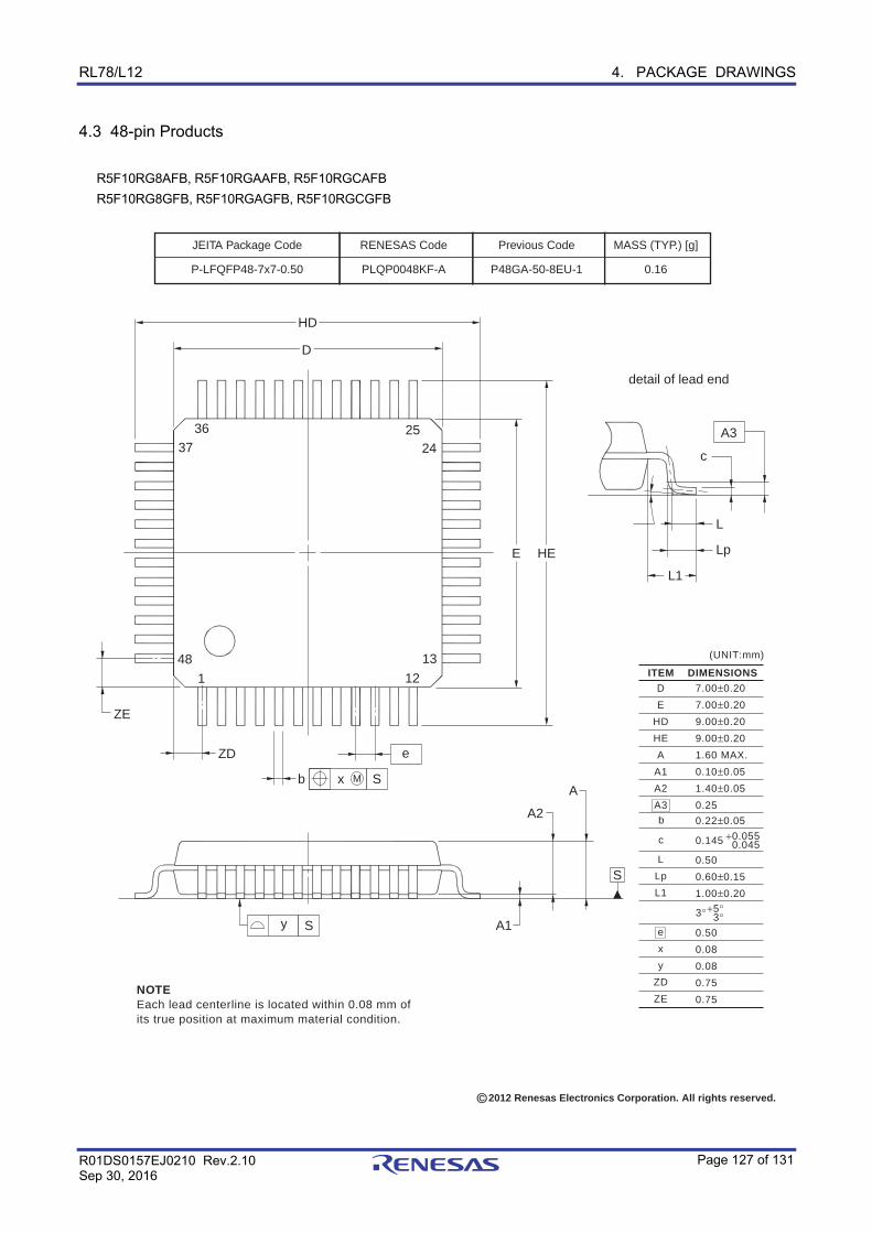
RL78/L12 4. PACKAGE DRAWINGS
R01DS0157EJ0210 Rev.2.10 Sep 30, 2016
Page 127 of 131
4.3 48-pin Products
R5F10RG8AFB, R5F10RGAAFB, R5F10RGCAFB
R5F10RG8GFB, R5F10RGAGFB, R5F10RGCGFB
JEITA Package Code RENESAS Code Previous Code MASS (TYP.) [g]
P-LFQFP48-7x7-0.50 PLQP0048KF-A P48GA-50-8EU-1 0.16
Sy
e
Sxb M
L
c
Lp
HD
HE
ZD
ZE
L1
A1
A2
A
D
E
A3
S
0.145 +0.0550.045
(UNIT:mm)
ITEM DIMENSIONS
D
E
HD
HE
A
A1
A2
A3
7.00±0.20
7.00±0.20
9.00±0.20
9.00±0.20
1.60 MAX.
0.10±0.05
1.40±0.05
0.25
c
e
x
y
ZD
ZE
0.50
0.08
0.08
0.75
0.75
L
Lp
L1
0.50
0.60±0.15
1.00±0.20
3°+5°3°
NOTEEach lead centerline is located within 0.08 mm ofits true position at maximum material condition.
detail of lead end
0.22±0.05b
12
24
1
48 13
2537
36
2012 Renesas Electronics Corporation. All rights reserved.
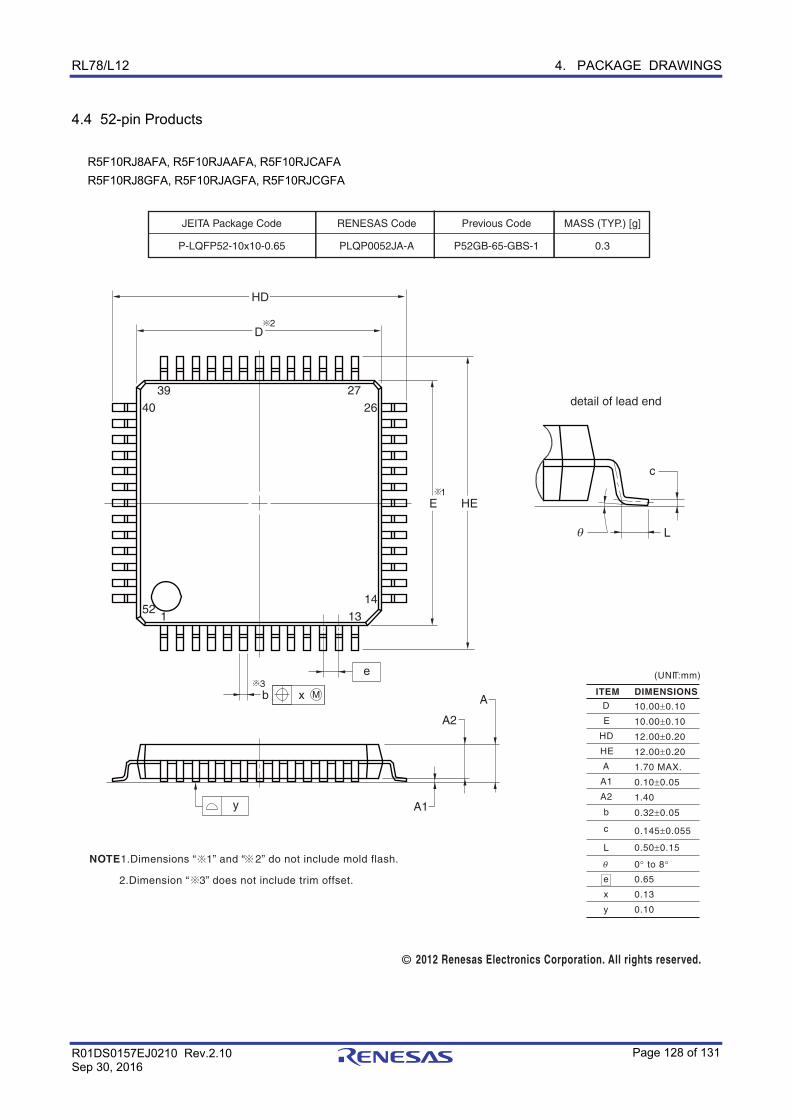
RL78/L12 4. PACKAGE DRAWINGS
R01DS0157EJ0210 Rev.2.10 Sep 30, 2016
Page 128 of 131
4.4 52-pin Products
R5F10RJ8AFA, R5F10RJAAFA, R5F10RJCAFA
R5F10RJ8GFA, R5F10RJAGFA, R5F10RJCGFA
y
e
xb M
L
c
HD
HE
A1
A2
A
D
E
(UNIT:mm)
ITEM DIMENSIONS
D
E
HD
HE
A
A1
A2
c
e
x
y
L
detail of lead end
b
13
26
152
14
2740
39
2
1
3
0.3
NOTE1.Dimensions “ 1” and “ 2” do not include mold flash.
2.Dimension “ 3” does not include trim offset.
JEITA Package Code
P-LQFP52-10x10-0.65
RENESAS Code
PLQP0052JA-A
Previous Code
P52GB-65-GBS-1
MASS (TYP.) [g]
10.00±0.10
10.00±0.10
12.00±0.20
12.00±0.20
1.70 MAX.
0.10±0.05
1.40
0.32±0.05
0.145±0.055
0.50±0.15
0° to 8°
0.65
0.13
0.10
2012 Renesas Electronics Corporation. All rights reserved.
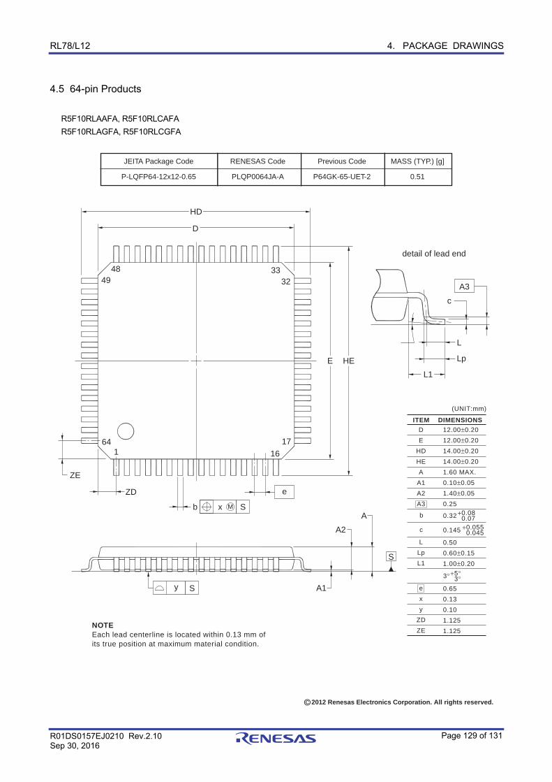
RL78/L12 4. PACKAGE DRAWINGS
R01DS0157EJ0210 Rev.2.10 Sep 30, 2016
Page 129 of 131
4.5 64-pin Products
R5F10RLAAFA, R5F10RLCAFA
R5F10RLAGFA, R5F10RLCGFA
JEITA Package Code RENESAS Code Previous Code MASS (TYP.) [g]
P-LQFP64-12x12-0.65 PLQP0064JA-A P64GK-65-UET-2 0.51
NOTEEach lead centerline is located within 0.13 mm ofits true position at maximum material condition.
detail of lead end
L
c
Lp
HD
HE
ZD
ZE
L1
A1
A2
A
D
E
16
32
164 17
3349
48
Sy
e
Sxb M
A3
S
0.145 +0.0550.045
(UNIT:mm)
ITEM DIMENSIONS
D
E
HD
HE
A
A1
A2
A3
12.00±0.20
12.00±0.20
14.00±0.20
14.00±0.20
1.60 MAX.
0.10±0.05
1.40±0.05
0.25
c
e
x
y
ZD
ZE
0.65
0.13
0.10
1.125
1.125
L
Lp
L1
0.50
0.60±0.15
1.00±0.20
3°+5°3°
0.32 +0.080.07b
2012 Renesas Electronics Corporation. All rights reserved.
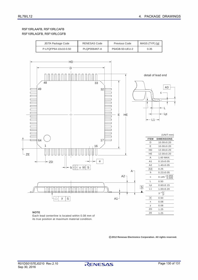
RL78/L12 4. PACKAGE DRAWINGS
R01DS0157EJ0210 Rev.2.10 Sep 30, 2016
Page 130 of 131
R5F10RLAAFB, R5F10RLCAFB
R5F10RLAGFB, R5F10RLCGFB
JEITA Package Code RENESAS Code Previous Code MASS (TYP.) [g]
P-LFQFP64-10x10-0.50 PLQP0064KF-A P64GB-50-UEU-2 0.35
Sy
e
Sxb M
L
c
Lp
HD
HE
ZD
ZE
L1
A1
A2
A
D
E
A3
S
0.145 +0.0550.045
(UNIT:mm)
ITEM DIMENSIONS
D
E
HD
HE
A
A1
A2
A3
10.00±0.20
10.00±0.20
12.00±0.20
12.00±0.20
1.60 MAX.
0.10±0.05
1.40±0.05
0.25
c
e
x
y
ZD
ZE
0.50
0.08
0.08
1.25
1.25
L
Lp
L1
0.50
0.60±0.15
1.00±0.20
3°+5°3°
NOTEEach lead centerline is located within 0.08 mm ofits true position at maximum material condition.
detail of lead end
0.22±0.05b
16
32
1
64 17
33
49
48
2012 Renesas Electronics Corporation. All rights reserved.
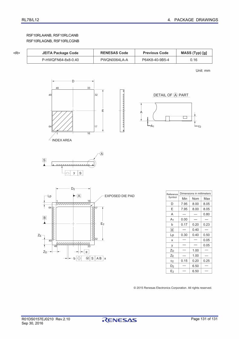
RL78/L12 4. PACKAGE DRAWINGS
R01DS0157EJ0210 Rev.2.10 Sep 30, 2016
Page 131 of 131
R5F10RLAANB, R5F10RLCANB
R5F10RLAGNB, R5F10RLCGNB
MASS (Typ) [g]
0.16
Unit: mm
Previous CodeRENESAS Code
PWQN0064LA-A P64K8-40-9B5-4
JEITA Package Code
P-HWQFN64-8x8-0.40
DEAA1
be
Lpxy
ZD
ZE
c2
D2
E2
7.957.95—
0.000.17
0.30
0.15
Min NomDimensions in millimetersReference
Symbol Max8.008.00
0.200.400.40
1.001.000.206.506.50
8.058.050.80
0.23
0.500.050.05
0.25
© 2015 Renesas Electronics Corporation. All rights reserved.
Sy
e
Lp
S xb A BM
A
D
E
48
32
33
16
17
1
64
A
S
B
A
D2
E2
49
EXPOSED DIE PAD
161
17
3249
64
INDEX AREA
A1 c2
ZD
ZE
3348
DETAIL OF A PART
—— —
— —
— ———
—
—
—— —
—
—
—
<R>
C - 1
Revision History RL78/L12 Datasheet
Rev. Date Description
Page Summary 0.01 Feb 20, 2012 - First Edition issued
0.02 Sep 26, 2012 7, 8 Modification of caution 2 in 1.3.5 64-pin products
15 Modification of I/O port in 1.6 Outline of Functions
- Modification of 2. ELECTRICAL SPECIFICATIONS (TARGET)
- Update of package drawings in 3. PACKAGE DRAWINGS
1.00 Jan 31, 2013 11 to 15 Modification of 1.5 Block Diagram
16 Modification of Note 2 in 1.6 Outline of Functions
17 Modification of 1.6 Outline of Functions
- Deletion of target in 2. ELECTRICAL SPECIFICATIONS
18 Addition of caution 2 to 2. ELECTRICAL SPECIFICATIONS
19 Addition of description, note 3, and remark 2 to 2.1 Absolute Maximum Ratings
20 Modification of description and addition of note to 2.1 Absolute Maximum Ratings
22, 23 Modification of 2.2 Oscillator Characteristics
30 Modification of notes 1 to 4 in 2.3.2 Supply current characteristics
32 Modification of notes 1, 3 to 6, 8 in 2.3.2 Supply current characteristics
34 Modification of notes 7, 9, 11, and addition of notes 8, 12 to 2.3.2 Supply current characteristics
36 Addition of description to 2.4 AC Characteristics
38, 40 to 42, 44 to 46, 48 to
52, 54, 55
Modification of 2.5.1 Serial array unit
57, 58 Modification of 2.5.2 Serial interface IICA
62 Modification of 2.6.2 Temperature sensor/internal reference voltage characteristics
64 Addition of note and caution in 2.6.5 Supply voltage rise time
69 Modification of 2.8 Data Memory STOP Mode Low Supply Voltage Data Retention Characteristics
69 Modification of conditions in 2.9 Timing Specs for Switching Flash Memory Programming Modes
70 Modification of 2.10 Timing Specifications for Switching Flash Memory Programming Modes
2.00 Jan 10, 2014 1 Modification of 1.1 Features 3 Modification of Figure 1-1 4 Modification of part number, note, and caution
5 to 10 Deletion of COMEXP pin in 1.3.1 to 1.3.5. 11 Modification of description in 1.4 Pin Identification
12 to 16 Deletion of COMEXP pin in 1.5.1 to 1.5.5 17 Modification of table and note 2 in 1.6 Outline of Functions 20 Modification of description in Absolute Maximum Ratings (TA = 25°C) (1/3) 21 Modification of description and note 2 in Absolute Maximum Ratings (TA = 25°C)
(2/3) 23 Modification of table, note, caution, and remark in 2.2.1 X1, XT1 oscillator
characteristics 23 Modification of table in 2.2.2 On-chip oscillator characteristics 24 Modification of table, notes 2 and 3 in 2.3.1 Pin characteristics (1/5) 25 Modification of notes 1 and 3 in 2.3.1 Pin characteristics (2/5) 30 Modification of notes 1 and 4 in 2.3.2 Supply current characteristics (1/3)
31, 32 Modification of table, notes 1, 5, and 6 in 2.3.2 Supply current characteristics (2/3)
33, 34 Modification of table, notes 1, 3, 4, and 5 to 10 in 2.3.2 Supply current characteristics (3/3)
C - 2
Rev. Date Description
Page Summary 2.00 Jan 10, 2014 35 Modification of table in 2.4 AC Characteristics
36 Addition of Minimum Instruction Execution Time during Main System Clock Operation
37 Modification of AC Timing Test Points and External System Clock Timing 39 Modification of AC Timing Test Points 39 Modification of description, notes 1 and 2 in (1) During communication at same
potential (UART mode) 41, 42 Modification of description, remark 2 in (2) During communication at same
potential (CSI mode) 42, 43 Modification of description in (3) During communication at same potential (CSI
mode) 45 Modification of description, notes 1 and 3, and remark 3 in (4) Communication at
different potential (1.8 V, 2.5 V, 3 V) (UART mode) (1/2) 46, 48 Modification of description, and remark 3 in (4) Communication at different
potential (1.8 V, 2.5 V, 3 V) (UART mode) (2/2) 49, 50 Modification of table, and note 1, caution, and remark 3 in (5) Communication at
different potential (2.5 V, 3 V) (CSI mode) 51 Modification of table and note in (6) Communication at different potential (1.8 V,
2.5 V, 3 V) (1/3) 52 Modification of table and notes 1 to 3 in (6) Communication at different potential
(1.8 V, 2.5 V, 3 V) (2/3) 53, 54 Modification of table, note 3, and remark 3 in (6) Communication at different
potential (1.8 V, 2.5 V, 3 V) (3/3) 56 Modification of table in (7) Communication at different potential (1.8 V, 2.5 V, 3 V)
(CSI mode) (1/2) 57 Modification of table in (7) Communication at different potential (1.8 V, 2.5 V, 3 V)
(CSI mode) (2/2) 59, 60 Addition of (1) I2C standard mode
61 Addition of (2) I2C fast mode 62 Addition of (3) I2C fast mode plus 63 Addition of table in 2.6.1 A/D converter characteristics
63, 64 Modification of description and notes 3 to 5 in 2.6.1 (1) 65 Modification of description, notes 3 and 4 in 2.6.1 (2) 66 Modification of description, notes 3 and 4 in 2.6.1 (3) 67 Modification of description, notes 3 and 4 in 2.6.1 (4) 67 Modification of the table in 2.6.2 Temperature sensor/internal reference voltage
characteristics 68 Modification of the table and note in 2.6.3 POR circuit characteristics 70 Modification of the table of LVD Detection Voltage of Interrupt & Reset Mode 70 Modification from VDD rise slope to Power supply voltage rising slope in 2.6.5
Supply voltage rise time 75 Modification of description in 2.10 Dedicated Flash Memory Programmer
Communication (UART) 76 Modification of the figure in 2.11 Timing Specifications for Switching Flash
Memory Programming Modes 77 to 126 Addition of products for industrial applications (G: TA = -40 to +105°C)
127 to 133 Addition of product names for industrial applications (G: TA = -40 to +105°C) 2.10 Sep 30, 2016 5 Modification of pin configuration in 1.3.1 32-pin products
6 Modification of pin configuration in 1.3.2 44-pin products 7 Modification of pin configuration in 1.3.3 48-pin products 8 Modification of pin configuration in 1.3.4 52-pin products
9, 10 Modification of pin configuration in 1.3.5 64-pin products 17 Modification of description of main system clock in 1.6 Outline of Functions 74 Modification of title of 2.8 RAM Data Retention Characteristics, Note, and figure 74 Modification of table of 2.9 Flash Memory Programming Characteristics 123 Modification of title of 3.8 RAM Data Retention Characteristics, Note, and figure 123 Modification of table of 3.9 Flash Memory Programming Characteristics and
addition of Note 4 131 Modification of 4.5 64-pin Products

C - 3
The mark “<R>” shows major revised points. The revised points can be easily searched by copying an “<R>” in the PDF file and specifying it in the “Find what:” field. All trademarks and registered trademarks are the property of their respective owners. SuperFlash is a registered trademark of Silicon Storage Technology, Inc. in several countries including the United States and Japan.
Caution: This product uses SuperFlash® technology licensed from Silicon Storage Technology, Inc.
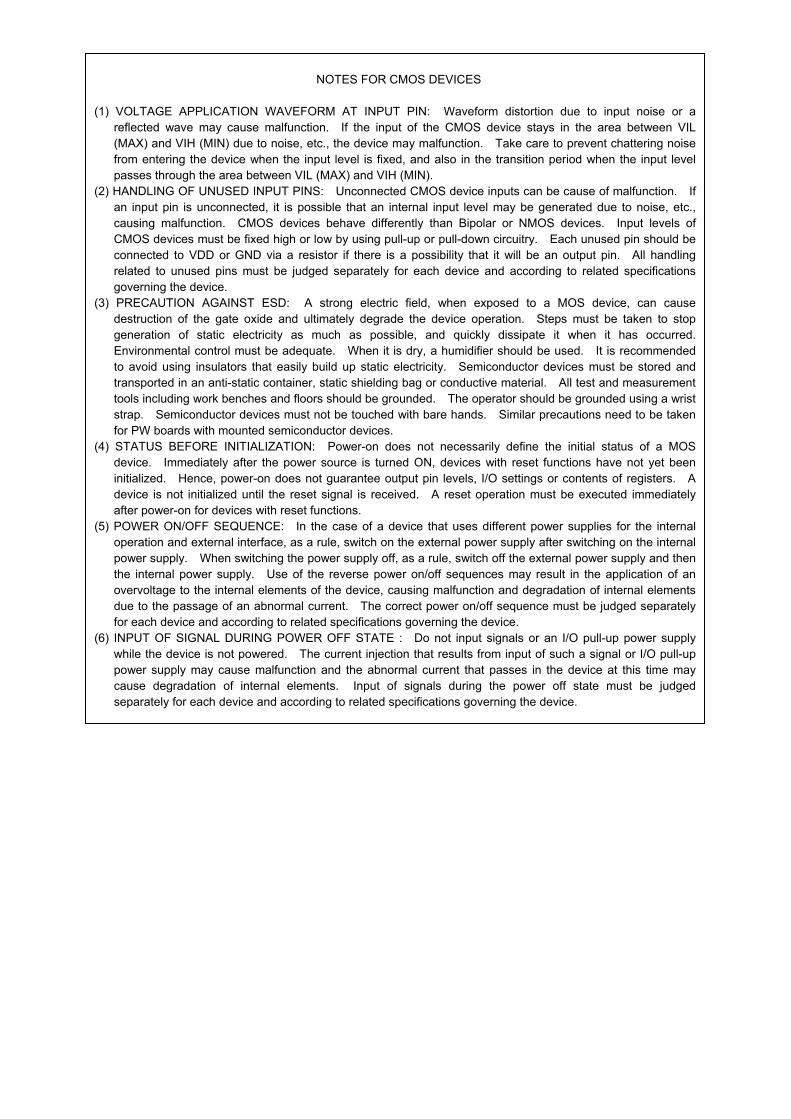
NOTES FOR CMOS DEVICES
(1) VOLTAGE APPLICATION WAVEFORM AT INPUT PIN: Waveform distortion due to input noise or a
reflected wave may cause malfunction. If the input of the CMOS device stays in the area between VIL (MAX) and VIH (MIN) due to noise, etc., the device may malfunction. Take care to prevent chattering noise from entering the device when the input level is fixed, and also in the transition period when the input level passes through the area between VIL (MAX) and VIH (MIN).
(2) HANDLING OF UNUSED INPUT PINS: Unconnected CMOS device inputs can be cause of malfunction. If an input pin is unconnected, it is possible that an internal input level may be generated due to noise, etc., causing malfunction. CMOS devices behave differently than Bipolar or NMOS devices. Input levels of CMOS devices must be fixed high or low by using pull-up or pull-down circuitry. Each unused pin should be connected to VDD or GND via a resistor if there is a possibility that it will be an output pin. All handling related to unused pins must be judged separately for each device and according to related specifications governing the device.
(3) PRECAUTION AGAINST ESD: A strong electric field, when exposed to a MOS device, can cause destruction of the gate oxide and ultimately degrade the device operation. Steps must be taken to stop generation of static electricity as much as possible, and quickly dissipate it when it has occurred. Environmental control must be adequate. When it is dry, a humidifier should be used. It is recommended to avoid using insulators that easily build up static electricity. Semiconductor devices must be stored and transported in an anti-static container, static shielding bag or conductive material. All test and measurement tools including work benches and floors should be grounded. The operator should be grounded using a wrist strap. Semiconductor devices must not be touched with bare hands. Similar precautions need to be taken for PW boards with mounted semiconductor devices.
(4) STATUS BEFORE INITIALIZATION: Power-on does not necessarily define the initial status of a MOS device. Immediately after the power source is turned ON, devices with reset functions have not yet been initialized. Hence, power-on does not guarantee output pin levels, I/O settings or contents of registers. A device is not initialized until the reset signal is received. A reset operation must be executed immediately after power-on for devices with reset functions.
(5) POWER ON/OFF SEQUENCE: In the case of a device that uses different power supplies for the internal operation and external interface, as a rule, switch on the external power supply after switching on the internal power supply. When switching the power supply off, as a rule, switch off the external power supply and then the internal power supply. Use of the reverse power on/off sequences may result in the application of an overvoltage to the internal elements of the device, causing malfunction and degradation of internal elements due to the passage of an abnormal current. The correct power on/off sequence must be judged separately for each device and according to related specifications governing the device.
(6) INPUT OF SIGNAL DURING POWER OFF STATE : Do not input signals or an I/O pull-up power supply while the device is not powered. The current injection that results from input of such a signal or I/O pull-up power supply may cause malfunction and the abnormal current that passes in the device at this time may cause degradation of internal elements. Input of signals during the power off state must be judged separately for each device and according to related specifications governing the device.
Notice1. Descriptions of circuits, software and other related information in this document are provided only to illustrate the operation of semiconductor products and application examples. You are fully responsible for
the incorporation of these circuits, software, and information in the design of your equipment. Renesas Electronics assumes no responsibility for any losses incurred by you or third parties arising from the
use of these circuits, software, or information.
2. Renesas Electronics has used reasonable care in preparing the information included in this document, but Renesas Electronics does not warrant that such information is error free. Renesas Electronics
assumes no liability whatsoever for any damages incurred by you resulting from errors in or omissions from the information included herein.
3. Renesas Electronics does not assume any liability for infringement of patents, copyrights, or other intellectual property rights of third parties by or arising from the use of Renesas Electronics products or
technical information described in this document. No license, express, implied or otherwise, is granted hereby under any patents, copyrights or other intellectual property rights of Renesas Electronics or
others.
4. You should not alter, modify, copy, or otherwise misappropriate any Renesas Electronics product, whether in whole or in part. Renesas Electronics assumes no responsibility for any losses incurred by you or
third parties arising from such alteration, modification, copy or otherwise misappropriation of Renesas Electronics product.
5. Renesas Electronics products are classified according to the following two quality grades: "Standard" and "High Quality". The recommended applications for each Renesas Electronics product depends on
the product's quality grade, as indicated below.
"Standard": Computers; office equipment; communications equipment; test and measurement equipment; audio and visual equipment; home electronic appliances; machine tools; personal electronic
equipment; and industrial robots etc.
"High Quality": Transportation equipment (automobiles, trains, ships, etc.); traffic control systems; anti-disaster systems; anti-crime systems; and safety equipment etc.
Renesas Electronics products are neither intended nor authorized for use in products or systems that may pose a direct threat to human life or bodily injury (artificial life support devices or systems, surgical
implantations etc.), or may cause serious property damages (nuclear reactor control systems, military equipment etc.). You must check the quality grade of each Renesas Electronics product before using it
in a particular application. You may not use any Renesas Electronics product for any application for which it is not intended. Renesas Electronics shall not be in any way liable for any damages or losses
incurred by you or third parties arising from the use of any Renesas Electronics product for which the product is not intended by Renesas Electronics.
6. You should use the Renesas Electronics products described in this document within the range specified by Renesas Electronics, especially with respect to the maximum rating, operating supply voltage
range, movement power voltage range, heat radiation characteristics, installation and other product characteristics. Renesas Electronics shall have no liability for malfunctions or damages arising out of the
use of Renesas Electronics products beyond such specified ranges.
7. Although Renesas Electronics endeavors to improve the quality and reliability of its products, semiconductor products have specific characteristics such as the occurrence of failure at a certain rate and
malfunctions under certain use conditions. Further, Renesas Electronics products are not subject to radiation resistance design. Please be sure to implement safety measures to guard them against the
possibility of physical injury, and injury or damage caused by fire in the event of the failure of a Renesas Electronics product, such as safety design for hardware and software including but not limited to
redundancy, fire control and malfunction prevention, appropriate treatment for aging degradation or any other appropriate measures. Because the evaluation of microcomputer software alone is very difficult,
please evaluate the safety of the final products or systems manufactured by you.
8. Please contact a Renesas Electronics sales office for details as to environmental matters such as the environmental compatibility of each Renesas Electronics product. Please use Renesas Electronics
products in compliance with all applicable laws and regulations that regulate the inclusion or use of controlled substances, including without limitation, the EU RoHS Directive. Renesas Electronics assumes
no liability for damages or losses occurring as a result of your noncompliance with applicable laws and regulations.
9. Renesas Electronics products and technology may not be used for or incorporated into any products or systems whose manufacture, use, or sale is prohibited under any applicable domestic or foreign laws or
regulations. You should not use Renesas Electronics products or technology described in this document for any purpose relating to military applications or use by the military, including but not limited to the
development of weapons of mass destruction. When exporting the Renesas Electronics products or technology described in this document, you should comply with the applicable export control laws and
regulations and follow the procedures required by such laws and regulations.
10. It is the responsibility of the buyer or distributor of Renesas Electronics products, who distributes, disposes of, or otherwise places the product with a third party, to notify such third party in advance of the
contents and conditions set forth in this document, Renesas Electronics assumes no responsibility for any losses incurred by you or third parties as a result of unauthorized use of Renesas Electronics
products.
11. This document may not be reproduced or duplicated in any form, in whole or in part, without prior written consent of Renesas Electronics.
12. Please contact a Renesas Electronics sales office if you have any questions regarding the information contained in this document or Renesas Electronics products, or if you have any other inquiries.
(Note 1) "Renesas Electronics" as used in this document means Renesas Electronics Corporation and also includes its majority-owned subsidiaries.
(Note 2) "Renesas Electronics product(s)" means any product developed or manufactured by or for Renesas Electronics.
http://www.renesas.comRefer to "http://www.renesas.com/" for the latest and detailed information.
Renesas Electronics America Inc.2801 Scott Boulevard Santa Clara, CA 95050-2549, U.S.A.Tel: +1-408-588-6000, Fax: +1-408-588-6130Renesas Electronics Canada Limited9251 Yonge Street, Suite 8309 Richmond Hill, Ontario Canada L4C 9T3Tel: +1-905-237-2004Renesas Electronics Europe LimitedDukes Meadow, Millboard Road, Bourne End, Buckinghamshire, SL8 5FH, U.KTel: +44-1628-585-100, Fax: +44-1628-585-900Renesas Electronics Europe GmbHArcadiastrasse 10, 40472 Düsseldorf, Germany Tel: +49-211-6503-0, Fax: +49-211-6503-1327Renesas Electronics (China) Co., Ltd.Room 1709, Quantum Plaza, No.27 ZhiChunLu Haidian District, Beijing 100191, P.R.ChinaTel: +86-10-8235-1155, Fax: +86-10-8235-7679Renesas Electronics (Shanghai) Co., Ltd.Unit 301, Tower A, Central Towers, 555 Langao Road, Putuo District, Shanghai, P. R. China 200333 Tel: +86-21-2226-0888, Fax: +86-21-2226-0999Renesas Electronics Hong Kong LimitedUnit 1601-1611, 16/F., Tower 2, Grand Century Place, 193 Prince Edward Road West, Mongkok, Kowloon, Hong KongTel: +852-2265-6688, Fax: +852 2886-9022Renesas Electronics Taiwan Co., Ltd.13F, No. 363, Fu Shing North Road, Taipei 10543, TaiwanTel: +886-2-8175-9600, Fax: +886 2-8175-9670Renesas Electronics Singapore Pte. Ltd.80 Bendemeer Road, Unit #06-02 Hyflux Innovation Centre, Singapore 339949Tel: +65-6213-0200, Fax: +65-6213-0300Renesas Electronics Malaysia Sdn.Bhd.Unit 1207, Block B, Menara Amcorp, Amcorp Trade Centre, No. 18, Jln Persiaran Barat, 46050 Petaling Jaya, Selangor Darul Ehsan, MalaysiaTel: +60-3-7955-9390, Fax: +60-3-7955-9510Renesas Electronics India Pvt. Ltd.No.777C, 100 Feet Road, HAL II Stage, Indiranagar, Bangalore, IndiaTel: +91-80-67208700, Fax: +91-80-67208777Renesas Electronics Korea Co., Ltd.12F., 234 Teheran-ro, Gangnam-Gu, Seoul, 135-080, KoreaTel: +82-2-558-3737, Fax: +82-2-558-5141
SALES OFFICES
© 2016 Renesas Electronics Corporation. All rights reserved.Colophon 5.0