Embed Size (px)
Citation preview

Datasheet AP6398S IEEE 802.11ac/a/b/g/n 2x2 WiFi with Bluetooth5.0
Combo Sip Module
1
AP6398S
Datasheet
All Rights Reserved. SparkLAN may make changes to specification and descriptions at any time without prior notice.
www.sparklan.com / [email protected] / +886 2 2659-1880
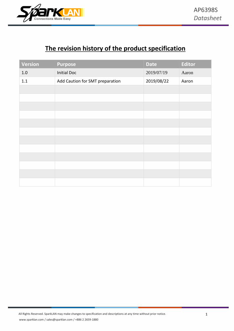
The revision history of the product specification
Version Purpose Date Editor
1.0 Initial Doc 2019/07/19 Aaron
1.1 Add Caution for SMT preparation 2019/08/22 Aaron

2
AP6398S
Datasheet
All Rights Reserved. SparkLAN may make changes to specification and descriptions at any time without prior notice.
www.sparklan.com / [email protected] / +886 2 2659-1880
Contents 1. Introduction .................................................................................................................................. 3
1.1 Product Overview ............................................................................................................................... 3 1.2 Product Feature ................................................................................................................................... 3
1.2.1 WLAN ....................................................................................................................................... 3
1.2.2 Bluetooth ................................................................................................................................. 3
2. Specification .................................................................................................................................. 4 2.1 General Specification ......................................................................................................................... 4 2.2 WiFi 2.4GHz RF Specification .......................................................................................................... 5 2.3 WiFi 5GHz RF Specification ............................................................................................................. 6 2.4 Bluetooth RF Specification ................................................................................................................ 9
3 Electrical Characteristics .............................................................................................................. 10 3.1 Absolute Maximum Ratings ............................................................................................................. 10 3.2 Recommended Operating Rating ...................................................................................................... 10 3.3 Recommended Operating Conditions and DC Characteristics ......................................................... 10
4. Host Interface Timing Diagram ..................................................................................................... 11 4.1 Power-up Sequence Timing Diagram ............................................................................................... 11 4.2 SDIO Default Mode Timing Diagram .............................................................................................. 14 4.3 SDIO High Speed Mode Timing Diagram ....................................................................................... 15 4.4 SDIO Bus Timing Specifications in SDR Modes ............................................................................ 16 4.5 SDIO Bus Timing Specifications in DDR50 Mode ......................................................................... 19
5. Power Consumption .................................................................................................................... 21 6. Block Diagram ............................................................................................................................. 23 7. Pin Definition ............................................................................................................................... 24
7.1 Pin Outline ........................................................................................................................................ 24 7.2 Pin Table ........................................................................................................................................... 25
8. Mechanical Specification ............................................................................................................. 27 8.1 Module Dimension ........................................................................................................................... 27 8.1 PCB Footprint ................................................................................................................................... 27
9. External Clock Reference.............................................................................................................. 29 9.1 SDIO Interface Description .............................................................................................................. 29
10. Recommended Reflow Profile ..................................................................................................... 30 10.1 Caution for SMT Preparation ......................................................................................................... 31
11. Package Information ................................................................................................................... 32 12. Order Information ...................................................................................................................... 34

3
AP6398S
Datasheet
All Rights Reserved. SparkLAN may make changes to specification and descriptions at any time without prior notice.
www.sparklan.com / [email protected] / +886 2 2659-1880
1. Introduction
1.1 Product Overview
AP6398S is a fully Wi-Fi and Bluetooth functionalities module with seamless roaming capabilities and
advance security, also it could interact with different vendors’ 802.11a/b/g/n/ac 2x2 Access Points with
MIMO standard and can accomplish up to speed of 867Mbps with dual stream in 802.11n to connect the
wireless LAN. Furthermore AP6398S included SDIO interface for Wi-Fi, UART/ PCM interface for
Bluetooth.
In addition, this compact module is a total solution for a combination of Wi-Fi + BT technologies. The
module is specifically developed for tablet, OTT box and portable devices.
1.2 Product Feature
1.2.1 WLAN
◼ TX and RX low-density parity check (LDPC) support for improved range and power efficiency.
◼ Dual-stream spatial multiplexing up to 867 Mbps data rate.
◼ 20, 40, 80 MHz channels with optional SGI (256 QAM modulation)
◼ Real simultaneous dual-band (RSDB)
◼ Supports 2 antennas with one for WLAN & Bluetooth shared port and one WLAN port. Also, shared
Bluetooth and WLAN receive signal path eliminates the need for an external power splitter while
maintaining excellent sensitivity for both Bluetooth and WLAN.
- Supports standard SDIO v3.0, compatible with SDIO v2.0 HOST interfaces.
1.2.2 Bluetooth
◼ BT host digital interface:
- HCI UART (up to 4 Mbps)
- PCM for audio data
◼ Complies with Bluetooth Core Specification Version 5.0 with provisions for supporting future
specifications. With Bluetooth Class 1 or Class2 transmitter operation.
◼ Supports extended synchronous connections (eSCO), for enhanced voice quality by allowing for
retransmission of dropped packets.

4
AP6398S
Datasheet
All Rights Reserved. SparkLAN may make changes to specification and descriptions at any time without prior notice.
www.sparklan.com / [email protected] / +886 2 2659-1880
2. Specification
2.1 General Specification
Standards
IEEE 802.11 ac/a/b/g/n 2T2R Wi-Fi + BT 5.0 Module
Bluetooth V5.0 , GFSK、DQPSK、8DPSK、LE(1Mbps)、2LE(2Mbps)
Chipset Broadcom
Operating Frequency 2.400 GHz ~ 2.4835 GHz (2.4GHz ISM Band) 5.15~5.35GHz、5.47~5.725GHz、5.725~5.85GHz (5GHz UNII Band)
Bluetooth: 2402 MHz ~ 2480 MHz
Modulation 802.11b : DQPSK、DBPSK、CCK
802.11 g/n : OFDM /64-QAM、16-QAM、QPSK、BPSK
802.11a : OFDM /64-QAM、16-QAM、QPSK、BPSK
802.11n : OFDM /64-QAM、16-QAM、QPSK、BPSK
802.11ac : OFDM /256-QAM、OFDM /64-QAM、16-QAM、QPSK、BPSK
Bluetooth: GFSK, π/4-DQPSK, 8DPSK
WiFi Interface SDIO 3.0 / 2.0
BT Interface
UART / PCM
Form Factor Stamp Type Antenna
External Dimension L x W : 15 x 13 (typical) mm 、 H : 1.85 (Maximum) mm
Operating temperature -30°C to 75°C
Storage temperature -40°C to 85°C
Humidity Operating Humidity 10% to 95% Non-Condensing
Driver Support Linux, Android
Note: The optimal RF performance specified in the data sheet, however, is guaranteed
only -10 °C to +55 °C and 3.2V < VBAT < 3.8V without derating performance.

5
AP6398S
Datasheet
All Rights Reserved. SparkLAN may make changes to specification and descriptions at any time without prior notice.
www.sparklan.com / [email protected] / +886 2 2659-1880
2.2 WiFi 2.4GHz RF Specification
Conditions : VBAT=3.3V ; VDDIO=3.3V ; Temp:25°C
Output Power , tolerance ± 1.5 dB The transmit EVM quality & spectrum mask are compliant with IEEE 802.11 standard
802.11b
1Mbps 2Mbps 5.5Mbps 11Mbps
17.5 17.5 17.5 17.5
802.11g
6、9Mbps 12、18Mbps 24Mbps 36Mbps 48Mbps
17.5 17.5 17 17 16.5
54Mbps
16.5
802.11n 20MHz
MCS0~2 MCS3 MCS4 MCS5 MCS6
17.5 16.5 16.5 16 16
MCS7
15.5
Note: The specifications of RF output power are subject to change to fulfill the safety regulation and requirements in end-user product.
Sensitivity, tolerance ± 2 dB CCK modulation PER ≦ 8%、OFDM modulation PER ≦ 10%
802.11b
Data Rate Spec.(dBm)
1Mbps -96
2Mbps -93
5.5Mbps -91
11Mbps -88
802.11g
SISO
Data Rate Spec.(dBm) Data Rate Spec.(dBm)
6Mbps -92 24Mbps -84
9Mbps -91 36Mbps -81
12Mbps -90 48Mbps -78
18Mbps -87 54Mbps -76
802.11g MIMO
Data Rate Spec.(dBm) Data Rate Spec.(dBm)
6Mbps -95 24Mbps -87
9Mbps -94 36Mbps -84
12Mbps -93 48Mbps -81
18Mbps -90 54Mbps -78
802.11n_20MHz SISO
Data Rate Spec.(dBm) Data Rate Spec.(dBm)
MCS0 -91 MCS4 -80
MCS1 -89 MCS4 -78
MCS2 -87 MCS6 -76
MCS3 -78 MCS7 -74

6
AP6398S
Datasheet
All Rights Reserved. SparkLAN may make changes to specification and descriptions at any time without prior notice.
www.sparklan.com / [email protected] / +886 2 2659-1880
802.11n_20MHz MIMO
Data Rate Spec.(dBm) Data Rate Spec.(dBm)
MCS0 -93 MCS5 -80
MCS1 -92 MCS6 -78
MCS2 -90 MCS7 -76
MCS3 -87 MCS8 -92
MCS4 -83 MCS15 -73
Maximum Input Level
802.11b : -10 dBm 802.11g/n : -20 dBm
2.3 WiFi 5GHz RF Specification
Conditions : VBAT=3.3V ; VDDIO=3.3V ; Temp:25°C
Output Power , tolerance ± 1.5 dB The transmit EVM quality & spectrum mask are compliant with IEEE 802.11 standard
802.11a
Frequency (MHz) 6~9Mbps 12~18Mbps 24Mbps 36Mbps
5150~5350 16.5 16.5 16 16
5470~5720 16.5 16.5 16 16
5725~5845 16.5 16.5 16 16
Frequency (MHz) 48Mbps 54Mbps
5150~5350 15.5 15.5
5470~5720 15.5 15.5
5725~5845 15.5 15.5
802.11n 20MHz
Frequency (MHz) MCS0~2 MCS3 MCS4 MCS5
5150~5350 16 16 15.5 15.5
5470~5720 16 16 15.5 15.5
5725~5845 16 16 15.5 15.5
Frequency (MHz) MCS6 MCS7
5150~5350 14.5 14.5
5470~5720 14.5 14.5
5725~5845 14.5 14.5
802.11n 40MHz
Frequency (MHz) MCS0~2 MCS3 MCS4 MCS5
5150~5350 16 16 15.5 15.5
5470~5720 16 16 15.5 15.5
5725~5845 16 16 15.5 15.5
Frequency (MHz) MCS6 MCS7
5150~5350 14.5 14.5
5470~5720 14.5 14.5
5725~5845 14.5 14.5
7
AP6398S
Datasheet
All Rights Reserved. SparkLAN may make changes to specification and descriptions at any time without prior notice.
www.sparklan.com / [email protected] / +886 2 2659-1880
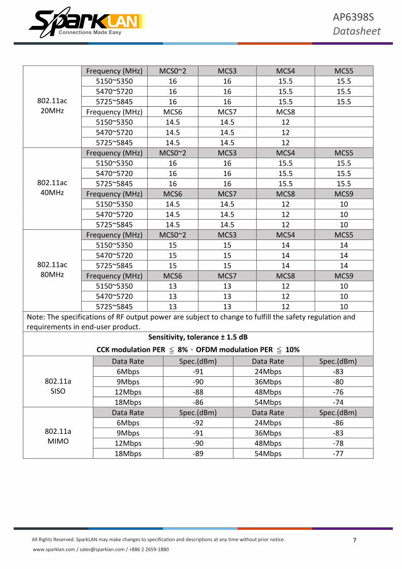
802.11ac 20MHz
Frequency (MHz) MCS0~2 MCS3 MCS4 MCS5
5150~5350 16 16 15.5 15.5
5470~5720 16 16 15.5 15.5
5725~5845 16 16 15.5 15.5
Frequency (MHz) MCS6 MCS7 MCS8
5150~5350 14.5 14.5 12
5470~5720 14.5 14.5 12
5725~5845 14.5 14.5 12
802.11ac 40MHz
Frequency (MHz) MCS0~2 MCS3 MCS4 MCS5
5150~5350 16 16 15.5 15.5
5470~5720 16 16 15.5 15.5
5725~5845 16 16 15.5 15.5
Frequency (MHz) MCS6 MCS7 MCS8 MCS9
5150~5350 14.5 14.5 12 10
5470~5720 14.5 14.5 12 10
5725~5845 14.5 14.5 12 10
802.11ac 80MHz
Frequency (MHz) MCS0~2 MCS3 MCS4 MCS5
5150~5350 15 15 14 14
5470~5720 15 15 14 14
5725~5845 15 15 14 14
Frequency (MHz) MCS6 MCS7 MCS8 MCS9
5150~5350 13 13 12 10
5470~5720 13 13 12 10
5725~5845 13 13 12 10
Note: The specifications of RF output power are subject to change to fulfill the safety regulation and requirements in end-user product.
Sensitivity, tolerance ± 1.5 dB
CCK modulation PER ≦ 8%、OFDM modulation PER ≦ 10%
802.11a SISO
Data Rate Spec.(dBm) Data Rate Spec.(dBm)
6Mbps -91 24Mbps -83
9Mbps -90 36Mbps -80
12Mbps -88 48Mbps -76
18Mbps -86 54Mbps -74
802.11a MIMO
Data Rate Spec.(dBm) Data Rate Spec.(dBm)
6Mbps -92 24Mbps -86
9Mbps -91 36Mbps -83
12Mbps -90 48Mbps -78
18Mbps -89 54Mbps -77

8
AP6398S
Datasheet
All Rights Reserved. SparkLAN may make changes to specification and descriptions at any time without prior notice.
www.sparklan.com / [email protected] / +886 2 2659-1880
802.11n_20MHz SISO
Data Rate Spec.(dBm) Data Rate Spec.(dBm)
MCS0 -90 MCS4 -79
MCS1 -88 MCS5 -76
MCS2 -86 MCS6 -73
MCS3 -83 MCS7 -72
802.11n_20MHz MIMO
Data Rate Spec.(dBm) Data Rate Spec.(dBm)
MCS0 -92 MCS5 -78
MCS1 -91 MCS6 -76
MCS2 -89 MCS7 -75
MCS3 -86 MCS8 -89
MCS4 -82 MCS15 -70
802.11n_40MHz SISO
Data Rate Spec.(dBm) Data Rate Spec.(dBm)
MCS0 -88 MCS4 -77
MCS1 -86 MCS5 -72
MCS2 -83 MCS6 -70
MCS3 -80 MCS7 -69
802.11n_40MHz MIMO
Data Rate Spec.(dBm) Data Rate Spec.(dBm)
MCS0 -88 MCS5 -75
MCS1 -88 MCS6 -73
MCS2 -86 MCS7 -72
MCS3 -83 MCS8 -86
MCS4 -79 MCS15 -67
802.11ac_20MHz SISO
Data Rate Spec.(dBm) Data Rate Spec.(dBm)
MCS0 -90 MCS5 -75
MCS1 -88 MCS6 -73
MCS2 -86 MCS7 -70
MCS3 -83 MCS8 -67
MCS4 -79
802.11ac_20MHz MIMO
Data Rate Spec.(dBm) Data Rate Spec.(dBm)
MCS0,NSS=1 -92 MCS6,NSS=1 -76
MCS1,NSS=1 -91 MCS7,NSS=1 -75
MCS2,NSS=1 -88 MCS8,NSS=1 -72
MCS3,NSS=1 -85 MCS0,NSS=2 -88
MCS4,NSS=1 -82 MCS8,NSS=2 -65
MCS5,NSS=1 -77
802.11ac_40MHz SISO
Data Rate Spec.(dBm) Data Rate Spec.(dBm)
MCS0 -88 MCS5 -72
MCS1 -86 MCS6 -70
MCS2 -83 MCS7 -69
MCS3 -80 MCS8 -65
MCS4 -76 MCS9 -63

9
AP6398S
Datasheet
All Rights Reserved. SparkLAN may make changes to specification and descriptions at any time without prior notice.
www.sparklan.com / [email protected] / +886 2 2659-1880
802.11ac_40MHz MIMO
Data Rate Spec.(dBm) Data Rate Spec.(dBm)
MCS0,NSS=1 -90 MCS6,NSS=1 -73
MCS1,NSS=1 -88 MCS7,NSS=1 -72
MCS2,NSS=1 -86 MCS8,NSS=1 -68
MCS3,NSS=1 -82 MCS9,NSS=1 -66
MCS4,NSS=1 -79 MCS0,NSS=2 -86
MCS5,NSS=1 -77 MCS9,NSS=2 -60
802.11ac_80MHz SISO
Data Rate Spec.(dBm) Data Rate Spec.(dBm)
MCS0 -85 MCS5 -68
MCS1 -82 MCS6 -67
MCS2 -79 MCS7 -65
MCS3 -76 MCS8 -62
MCS4 -73 MCS9 -60
802.11ac_80MHz MIMO
Data Rate Spec.(dBm) Data Rate Spec.(dBm)
MCS0,NSS=1 -87 MCS6,NSS=1 -70
MCS1,NSS=1 -85 MCS7,NSS=1 -68
MCS2,NSS=1 -82 MCS8,NSS=1 -66
MCS3,NSS=1 -79 MCS9,NSS=1 -63
MCS4,NSS=1 -76 MCS0,NSS=2 -83
MCS5,NSS=1 -71 MCS9,NSS=2 -58
Maximum Input Level
802.11a/n/ac : -30 dBm
2.4 Bluetooth RF Specification Conditions : VBAT=3.3V ; VDDIO=3.3V ; Temp:25°C
RF Specification
Min. Typical. Max.
Output Power* 0 7 10
Sensitivity @ BER=0.1% for GFSK (1Mbps)
-86 dBm
Sensitivity @ BER=0.01% for π/4-DQPSK (2Mbps)
-88 dBm
Sensitivity @ BER=0.01% for 8DPSK (3Mbps)
-84 dBm
Sensitivity @ BER=0.01% for LE (1Mbps)
-89 dBm
Sensitivity @ BER=0.01% for 2LE (2Mbps)
TBD
Maximum Input Level GFSK (1Mbps):-20dBm π/4-DQPSK (2Mbps) :-20dBm 8DPSK (3Mbps) :-20dBm
Note*:The Bluetooth BDR output power is able to be configured by firmware (hcd file).

10
AP6398S
Datasheet
All Rights Reserved. SparkLAN may make changes to specification and descriptions at any time without prior notice.
www.sparklan.com / [email protected] / +886 2 2659-1880
3 Electrical Characteristics
3.1 Absolute Maximum Ratings
Symbol Description Min. Max. Unit
VBAT Input supply Voltage -0.5 4.5 V
VDDIO Digital/Bluetooth/SDIO/ I/O Voltage -0.5 3.8 V
3.2 Recommended Operating Rating The module requires two power supplies: VBAT and VDDIO.
Voltage rails Min. Typ. Max. Unit
VBAT 3.0 3.3 3.8 V
VDDIO 1.7 1.8,3.3 3.6 V
VBAT current consumption 1200mA (Peak), when VBAT = 3.3V
3.3 Recommended Operating Conditions and DC Characteristics Value
Parameter Symbol Minimum Typical Maximum Unit
DC supply voltage for VBAT VBAT 3.0a - 5.25 V
DC supply voltage for core VDD 1.14 1.2 1.26 V
DC supply voltage for RF blocks in chip VDDRF 1.14 1.2 1.26 V
DC supply voltage for TCXO input buffer WRF_TCXO_VDD 1.62 1.8 1.98 V
DC supply voltage for Digital I/O VDDIO VDDIO_SD
1.62 - 3.63 V
DC supply voltage for RF switch I/Os VDDIO_RF
TSSI 3.13 3.3 3.46 V
External TSSI input 0.15 - 0.95 V
Internal POR threshold Vth_POR 0.4 - 0.7 V
DC supply voltage for WCC I/O WCC_VDDIO 1.62 - 3.63 V
SDIO Interface I/O pins and PCIe Out-of Band Signals (PCIE_PERST_L, PCIE_PME_L, and PCIE_CLKREQ_L)
For VDDIO = 1.8V
Input high voltage VIH 1.27 -- - V
Input low voltage VIL - - 0.58 V
Output high Voltage @ 2 mA VOH 1.40 - V
Output Low Voltage @ 2 mA VOL - - 0.45 V
For VDDIO_SD = 3.3V
Input high Voltage VIH 0.625 x VDDIO
- - V
Input low Voltage VIL - - 0.25 x VDDIO
V

11
AP6398S
Datasheet
All Rights Reserved. SparkLAN may make changes to specification and descriptions at any time without prior notice.
www.sparklan.com / [email protected] / +886 2 2659-1880
Output high voltage @2mA VOH 0.75 x VDDIO
- - V
Output Low Voltage @2mA VOL - - 0.125 x VDDIO
V
Other Digital I/O Pins
For VDDIO=1.8V
Input high voltage VIH 0.65 x VDDIO
- - V
Input low voltage VIL - - 0.35 x VDDIO
V
Output high voltage @2mA VOH VDDIO-0.45
- - V
Output low voltage @2mA VOL - - 0.45 V
For VDDIO=3.3V - - -
Input high voltage VIH 2.00 - - V
Input low voltage VIL - - 0.80 V
Output high voltage@2mA VOH VDDIO-0.4 - - V
Output low voltage@2mA VOL - - 0.4 V
RF Switch Control Output Pinsb
For VDDIO_RF=3.3V
Output high voltage@2mA VOH VDDIO-0.4 - - V
Output low voltage@2mA VOL - - 0.4 V
Input capacitance CIN - - 5 pF
4. Host Interface Timing Diagram
4.1 Power-up Sequence Timing Diagram
The module has signals that allow the host to control power consumption by enabling or disabling the
Bluetooth, WLAN and internal regulator blocks. These signals are described below.
Additionally, diagrams are provided to indicate proper sequencing of the signals for carious operating
states. The timing value indicated are minimum required values: longer delays are also acceptable.
◼ WL_REG_ON: Used by the PMU to power up or power down the internal regulators used by the
WLAN section. When this pin is high, the regulators are enabled and the WLAN section is out of reset.
When this pin is low the WLAN section is in reset.
◼ BT_REG_ON: Used by the PMU to power up or power down the internal regulators used by the BT
section. Low asserting reset for Bluetooth. This pin has no effect on WLAN and does not control any
PMU functions. This pin must be driven high or low (not left floating).

12
AP6398S
Datasheet
All Rights Reserved. SparkLAN may make changes to specification and descriptions at any time without prior notice.
www.sparklan.com / [email protected] / +886 2 2659-1880

13
AP6398S
Datasheet
All Rights Reserved. SparkLAN may make changes to specification and descriptions at any time without prior notice.
www.sparklan.com / [email protected] / +886 2 2659-1880
14
AP6398S
Datasheet
All Rights Reserved. SparkLAN may make changes to specification and descriptions at any time without prior notice.
www.sparklan.com / [email protected] / +886 2 2659-1880
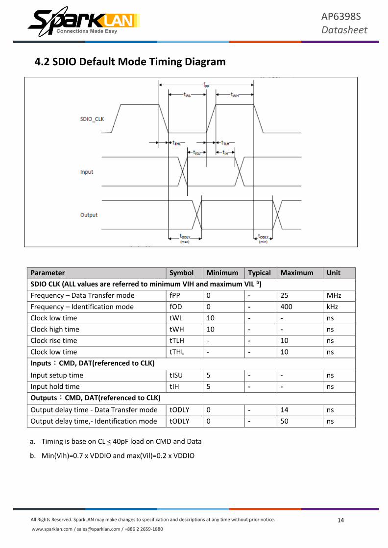
4.2 SDIO Default Mode Timing Diagram
Parameter Symbol Minimum Typical Maximum Unit
SDIO CLK (ALL values are referred to minimum VIH and maximum VIL b)
Frequency – Data Transfer mode fPP 0 - 25 MHz
Frequency – Identification mode fOD 0 - 400 kHz
Clock low time tWL 10 - - ns
Clock high time tWH 10 - - ns
Clock rise time tTLH - - 10 ns
Clock low time tTHL - - 10 ns
Inputs:CMD, DAT(referenced to CLK)
Input setup time tISU 5 - - ns
Input hold time tIH 5 - - ns
Outputs:CMD, DAT(referenced to CLK)
Output delay time - Data Transfer mode tODLY 0 - 14 ns
Output delay time,- Identification mode tODLY 0 - 50 ns
a. Timing is base on CL < 40pF load on CMD and Data
b. Min(Vih)=0.7 x VDDIO and max(Vil)=0.2 x VDDIO
15
AP6398S
Datasheet
All Rights Reserved. SparkLAN may make changes to specification and descriptions at any time without prior notice.
www.sparklan.com / [email protected] / +886 2 2659-1880
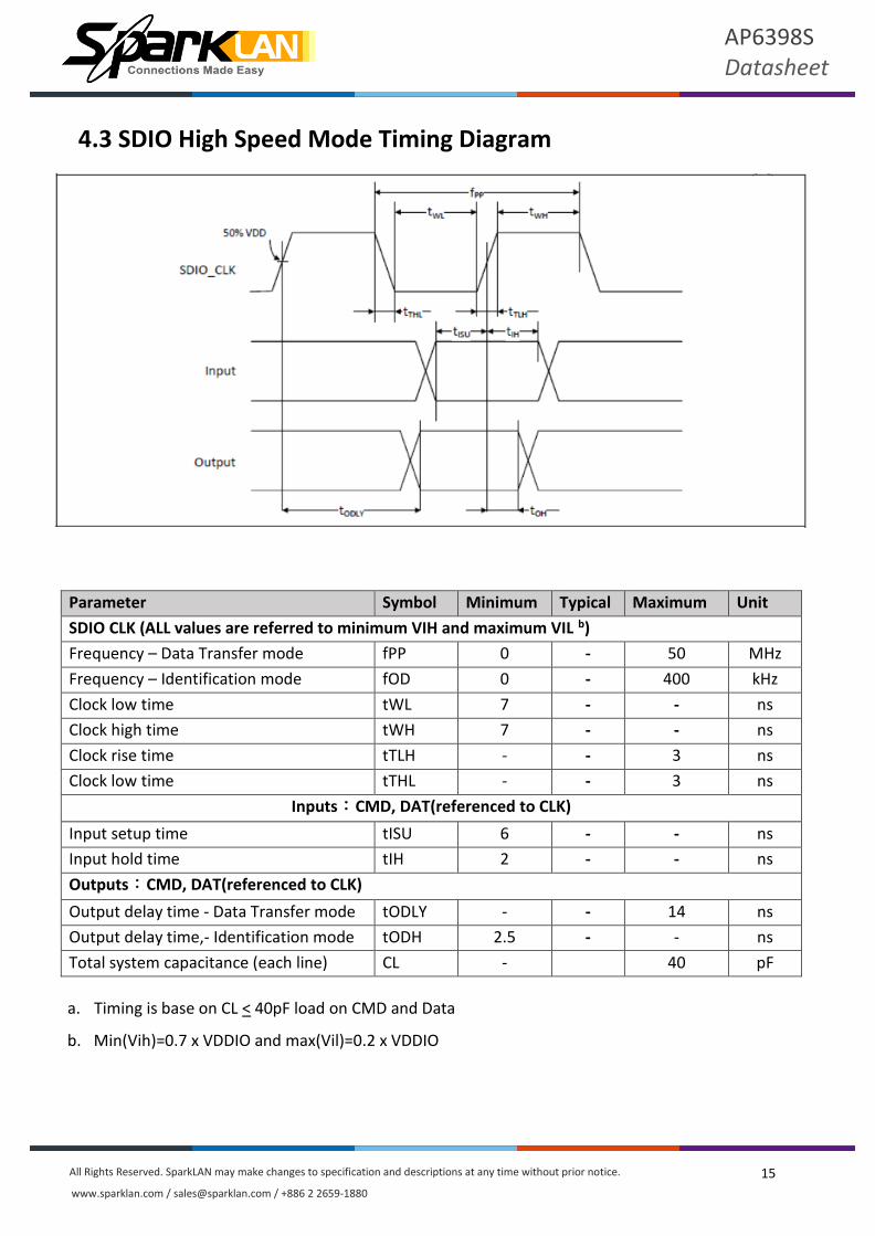
4.3 SDIO High Speed Mode Timing Diagram
Parameter Symbol Minimum Typical Maximum Unit
SDIO CLK (ALL values are referred to minimum VIH and maximum VIL b)
Frequency – Data Transfer mode fPP 0 - 50 MHz
Frequency – Identification mode fOD 0 - 400 kHz
Clock low time tWL 7 - - ns
Clock high time tWH 7 - - ns
Clock rise time tTLH - - 3 ns
Clock low time tTHL - - 3 ns
Inputs:CMD, DAT(referenced to CLK)
Input setup time tISU 6 - - ns
Input hold time tIH 2 - - ns
Outputs:CMD, DAT(referenced to CLK)
Output delay time - Data Transfer mode tODLY - - 14 ns
Output delay time,- Identification mode tODH 2.5 - - ns
Total system capacitance (each line) CL - 40 pF
a. Timing is base on CL < 40pF load on CMD and Data
b. Min(Vih)=0.7 x VDDIO and max(Vil)=0.2 x VDDIO

16
AP6398S
Datasheet
All Rights Reserved. SparkLAN may make changes to specification and descriptions at any time without prior notice.
www.sparklan.com / [email protected] / +886 2 2659-1880
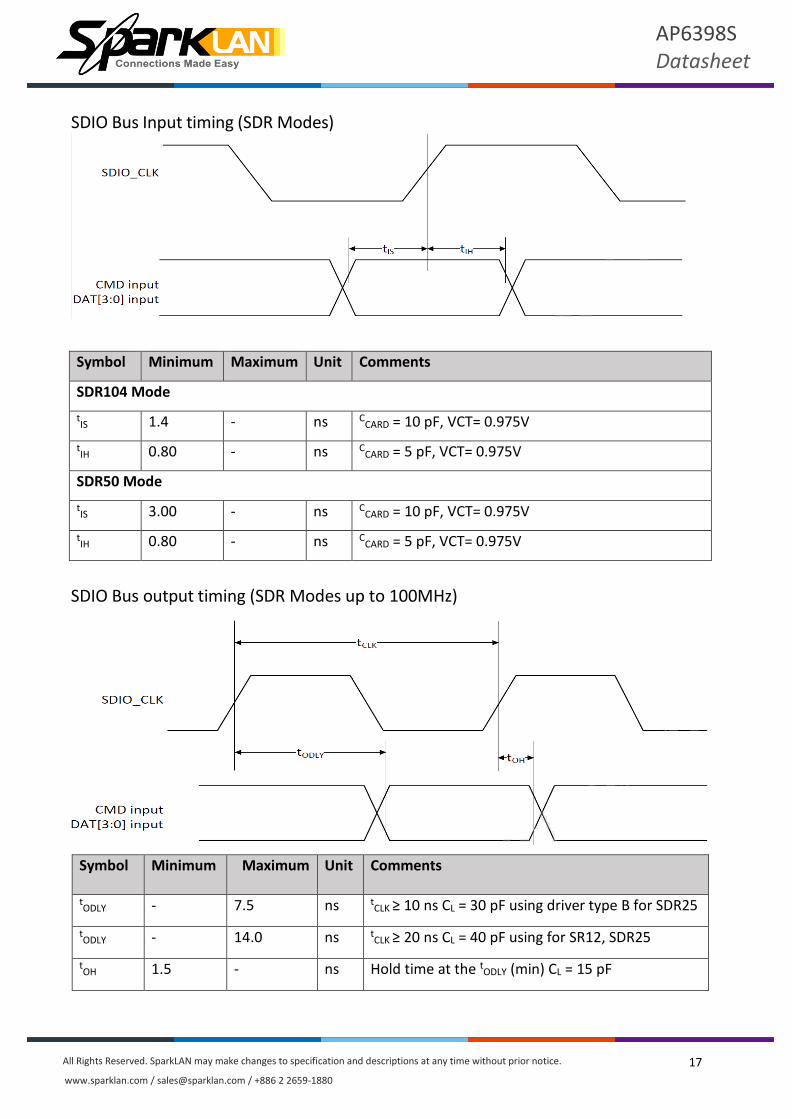
4.4 SDIO Bus Timing Specifications in SDR Modes
Parameter Symbol Minimum Maximum Unit Comments
- tCLK 40 - ns SDR12 mode
20 - ns SDR25mode
10 - ns SDR50 mode
4.8 - ns SDR104 mode
- tCR,t
CF - 0.2 x tCLK ns t
CR,tCF < 2.00 ns (max) @100MHz,
CCARD = 10 pF
tCR,t
CF < 0.96 ns (max) @208MHz,
CCARD = 10 pF
Clock duty - 30 70 % -
17
AP6398S
Datasheet
All Rights Reserved. SparkLAN may make changes to specification and descriptions at any time without prior notice.
www.sparklan.com / [email protected] / +886 2 2659-1880
SDIO Bus Input timing (SDR Modes)
Symbol Minimum Maximum Unit Comments
SDR104 Mode
tIS 1.4 - ns C
CARD = 10 pF, VCT= 0.975V
tIH 0.80 - ns C
CARD = 5 pF, VCT= 0.975V
SDR50 Mode
tIS 3.00 - ns C
CARD = 10 pF, VCT= 0.975V
tIH 0.80 - ns C
CARD = 5 pF, VCT= 0.975V
SDIO Bus output timing (SDR Modes up to 100MHz)
Symbol Minimum Maximum Unit Comments
tODLY - 7.5 ns t
CLK ≥ 10 ns CL = 30 pF using driver type B for SDR25
tODLY - 14.0 ns t
CLK ≥ 20 ns CL = 40 pF using for SR12, SDR25
tOH 1.5 - ns Hold time at the tODLY (min) CL = 15 pF

18
AP6398S
Datasheet
All Rights Reserved. SparkLAN may make changes to specification and descriptions at any time without prior notice.
www.sparklan.com / [email protected] / +886 2 2659-1880
Card output timing (SDR Modes 100MHz to 208MHz)
Symbol Minimum Maximum Unit Comments
tOP 0 2 UI Card output phase
△tOP -350 +1550 ps Delay variation due to temo. change after tuning
△tODW 0.60 - UI tODW = 2.88 ns @ 208MHz
◼ △tOP = +1550 ps for junction temperature of △t
OP = 90 degrees during operation
◼ △tOP = -350 ps for junction temperature of △t
OP = -20 degrees during operation
◼ △tOP = +2600 ps for junction temperature of △t
OP = -20 to +125 degrees during operation

19
AP6398S
Datasheet
All Rights Reserved. SparkLAN may make changes to specification and descriptions at any time without prior notice.
www.sparklan.com / [email protected] / +886 2 2659-1880
Consideration for Variable Data Window (SDR 104 Mode)
4.5 SDIO Bus Timing Specifications in DDR50 Mode
Parameter Symbol Minimum Maximum Unit Comments
- tCLK 20 - ns DDR50 mode
- tCR,t
CF - 0.2 x tCLK ns tCR, tCF <4.00 ns(max) @ 50MHz
CCARD= 10 pF
Clock duty - 45 55 % -
20
AP6398S
Datasheet
All Rights Reserved. SparkLAN may make changes to specification and descriptions at any time without prior notice.
www.sparklan.com / [email protected] / +886 2 2659-1880
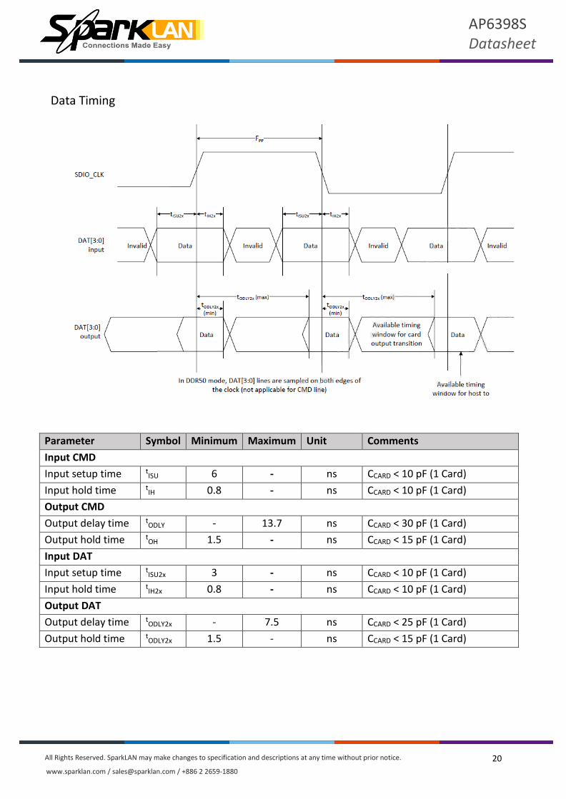
Data Timing
Parameter Symbol Minimum Maximum Unit Comments
Input CMD
Input setup time tISU
6 - ns CCARD < 10 pF (1 Card)
Input hold time tIH
0.8 - ns CCARD < 10 pF (1 Card)
Output CMD
Output delay time tODLY
- 13.7 ns CCARD < 30 pF (1 Card)
Output hold time tOH
1.5 - ns CCARD < 15 pF (1 Card)
Input DAT
Input setup time tISU2x
3 - ns CCARD < 10 pF (1 Card)
Input hold time tIH2x
0.8 - ns CCARD < 10 pF (1 Card)
Output DAT
Output delay time tODLY2x - 7.5 ns CCARD < 25 pF (1 Card)
Output hold time tODLY2x 1.5 - ns CCARD < 15 pF (1 Card)

21
AP6398S
Datasheet
All Rights Reserved. SparkLAN may make changes to specification and descriptions at any time without prior notice.
www.sparklan.com / [email protected] / +886 2 2659-1880
5. Power Consumption
◼ 2.4 GHz
Test Mode DUT Status Supply Voltage (VDDIO 3.3V )
Supply Voltage (VBAT 3.3V )
802.11b 11Mbps
Continue TX(SISO) 0.8mA 270 mA
Continue RX(SISO) 0.8mA 75 mA
802.11b 11Mbps
Continue TX(CDD) 0.8 mA 510 mA
Continue RX(CDD) 0.8 mA 110 mA
802.11g 54Mbps
Continue TX (SISO) 0.8 mA 220 mA
Continue RX(SISO) 0.8 mA 75 mA
Continue TX (CDD) 0.8 mA 410 mA
Continue RX(CDD) 0.8 mA 110 mA
802.11n
MCS7
Continue TX HT20(SISO) 0.8 mA 200 mA
Continue RX HT20 (SISO) 0.8 mA 75 mA
Continue TX HT20 (CDD) 0.8 mA 380 mA
Continue RX HT20 (CDD) 0.8 mA 110 mA
Bluetooth
Continue TX 0.21 mA 13 mA
Continue RX 0.21 mA 12 mA
(Unit: mA)
◼ 5GHz
Test Mode DUT Status Supply Voltage (VDDIO 3.3V )
Supply Voltage (VBAT 3.3V )
802.11a 54Mbps
Continue TX (SISO) 0.8 mA 250 mA
Continue RX(SISO) 0.8 mA 110 mA
Continue TX (CDD) 0.8 mA 466 mA
Continue RX(CDD) 0.8 mA 140 mA
802.11n MCS7
Continue TX HT20(SISO) 0.8 mA 240 mA
Continue RX HT20 (SISO) 0.8 mA 110 mA
Continue TX HT20 (CDD) 0.8 mA 440 mA
Continue RX HT20 (CDD) 0.8 mA 140 mA
Continue TX HT40(SISO) 0.8 mA 253 mA
Continue RX HT40 (SISO) 0.8 mA 130 mA
Continue TX HT40 (CDD) 0.8 mA 410 mA
Continue RX HT40 (CDD) 0.8 mA 160 mA
(Unit: mA)
22
AP6398S
Datasheet
All Rights Reserved. SparkLAN may make changes to specification and descriptions at any time without prior notice.
www.sparklan.com / [email protected] / +886 2 2659-1880
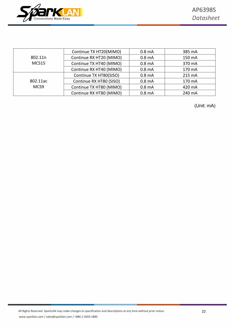
802.11n MCS15
Continue TX HT20(MIMO) 0.8 mA 385 mA
Continue RX HT20 (MIMO) 0.8 mA 150 mA
Continue TX HT40 (MIMO) 0.8 mA 370 mA
Continue RX HT40 (MIMO) 0.8 mA 170 mA
802.11ac
MCS9
Continue TX HT80(SISO) 0.8 mA 215 mA
Continue RX HT80 (SISO) 0.8 mA 170 mA
Continue TX HT80 (MIMO) 0.8 mA 420 mA
Continue RX HT80 (MIMO) 0.8 mA 240 mA
(Unit: mA)

23
AP6398S
Datasheet
All Rights Reserved. SparkLAN may make changes to specification and descriptions at any time without prior notice.
www.sparklan.com / [email protected] / +886 2 2659-1880
6. Block Diagram

24
AP6398S
Datasheet
All Rights Reserved. SparkLAN may make changes to specification and descriptions at any time without prior notice.
www.sparklan.com / [email protected] / +886 2 2659-1880
7. Pin Definition
7.1 Pin Outline
25
AP6398S
Datasheet
All Rights Reserved. SparkLAN may make changes to specification and descriptions at any time without prior notice.
www.sparklan.com / [email protected] / +886 2 2659-1880
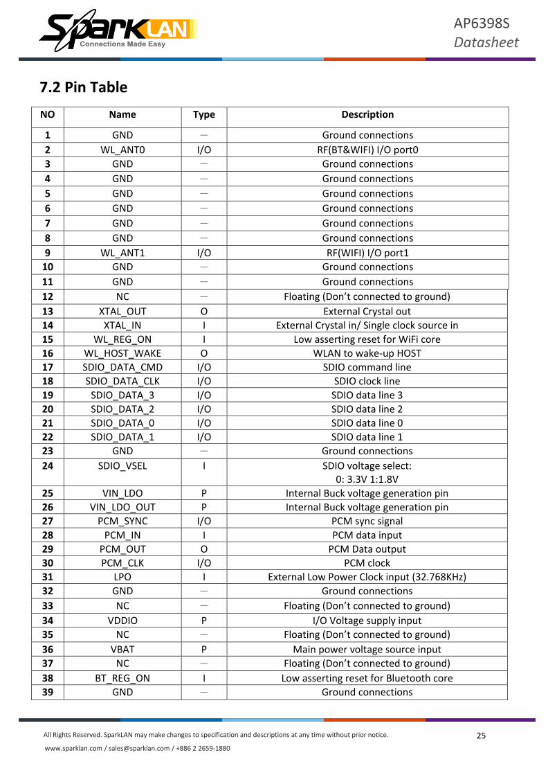
7.2 Pin Table
NO Name Type Description
1 GND - Ground connections
2 WL_ANT0 I/O RF(BT&WIFI) I/O port0
3 GND - Ground connections
4 GND - Ground connections
5 GND - Ground connections
6 GND - Ground connections
7 GND - Ground connections
8 GND - Ground connections
9 WL_ANT1 I/O RF(WIFI) I/O port1
10 GND - Ground connections
11 GND - Ground connections
12 NC - Floating (Don’t connected to ground)
13 XTAL_OUT O External Crystal out
14 XTAL_IN I External Crystal in/ Single clock source in
15 WL_REG_ON I Low asserting reset for WiFi core
16 WL_HOST_WAKE O WLAN to wake-up HOST
17 SDIO_DATA_CMD I/O SDIO command line
18 SDIO_DATA_CLK I/O SDIO clock line
19 SDIO_DATA_3 I/O SDIO data line 3
20 SDIO_DATA_2 I/O SDIO data line 2
21 SDIO_DATA_0 I/O SDIO data line 0
22 SDIO_DATA_1 I/O SDIO data line 1
23 GND - Ground connections
24 SDIO_VSEL I SDIO voltage select: 0: 3.3V 1:1.8V
25 VIN_LDO P Internal Buck voltage generation pin
26 VIN_LDO_OUT P Internal Buck voltage generation pin
27 PCM_SYNC I/O PCM sync signal
28 PCM_IN I PCM data input
29 PCM_OUT O PCM Data output
30 PCM_CLK I/O PCM clock
31 LPO I External Low Power Clock input (32.768KHz)
32 GND - Ground connections
33 NC - Floating (Don’t connected to ground)
34 VDDIO P I/O Voltage supply input
35 NC - Floating (Don’t connected to ground)
36 VBAT P Main power voltage source input
37 NC - Floating (Don’t connected to ground)
38 BT_REG_ON I Low asserting reset for Bluetooth core
39 GND - Ground connections

26
AP6398S
Datasheet
All Rights Reserved. SparkLAN may make changes to specification and descriptions at any time without prior notice.
www.sparklan.com / [email protected] / +886 2 2659-1880
40 UART_TXD O Bluetooth UART interface
41 UART_RXD I Bluetooth UART interface
42 UART_RTS_N O Bluetooth UART interface
43 UART_CTS_N I Bluetooth UART interface
44 WL_UART_TX O WL_UART_TX
45 WL_UART_RX I WL_UART_RX
46 NC - Floating (Don’t connected to ground)
47 GND - Ground connections
48 NC - Floating (Don’t connected to ground)
49 BT_WAKE I HOST wake-up Bluetooth device
50 BT_HOST_WAKE O Bluetooth device to wake-up HOST
27
AP6398S
Datasheet
All Rights Reserved. SparkLAN may make changes to specification and descriptions at any time without prior notice.
www.sparklan.com / [email protected] / +886 2 2659-1880
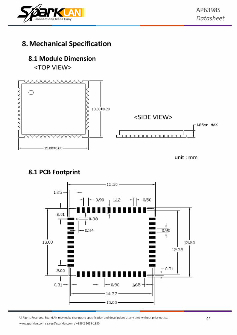
8. Mechanical Specification
8.1 Module Dimension
8.1 PCB Footprint

28
AP6398S
Datasheet
All Rights Reserved. SparkLAN may make changes to specification and descriptions at any time without prior notice.
www.sparklan.com / [email protected] / +886 2 2659-1880
◼ Solder paste layer design is generally the same as recommended footprint.
(錫膏層設計通常建議和焊墊尺寸相同)
◼ If soldering quality with good wetting on upright side is essential for PQC, how to optimize the
aperture design in the stencil to adjust the amount of solder paste would be crucial.
In addition, a kind of stencil design with stepped thickness in partial area would be considered if the
thickness of stencil is about 0.1mm or thinner. Please optimize the stencil design by manufacture
engineer or contact SparkLAN FAE for assistance.
(如果模組吃錫品質考量側面爬錫,如何優化鋼網開孔設計以調整適當的錫膏量是非常重要
的。尤其鋼網的厚度大約是 0.1mm或更薄時,可考慮局部加厚鋼網的設計。請諮詢製程工程
師以優化鋼網的設計,或是聯絡速連通訊技術支持團隊).

29
AP6398S
Datasheet
All Rights Reserved. SparkLAN may make changes to specification and descriptions at any time without prior notice.
www.sparklan.com / [email protected] / +886 2 2659-1880
9. External Clock Reference
External LPO signal characteristics
Parameter Specification Units
Nominal input frequency 32.768 kHz
Frequency accuracy +/-30 ppm
Duty cycle 30 - 70 %
Input signal amplitude 1600 to 3300 mV, p-p
Signal type Square-wave or sine-wave -
Input impedance >100k <5
pF
Clock jitter (integrated over 300Hz – 15KHz) <1 Hz
Output high voltage 0.7Vio - Vio V
9.1 SDIO Interface Description
The module supports SDIO version 3.0 for all 1.8V 4-bit UHSI speeds: SDR50 (100 Mbps),SDR104(208MHz)
and DDR50(50MHz, dual rates) in addition to the 3.3V default speed(25MHz) and high speed (50 MHz). It
has the ability to stop the SDIO clock and map the interrupt signal into a GPIO pin. This ‘out-of-band’
interrupt signal notifies the host when the WLAN device wants to turn on the SDIO interface. The ability to
force the control of the gated clocks from within the WLAN chip is also provided.
◼ Function 0 Standard SDIO function (Max BlockSize / ByteCount = 32B)
◼ Function 1 Backplane Function to access the internal System On Chip (SOC) address space (Max
BlockSize / ByteCount = 64B)
◼ Function 2 WLAN Function for efficient WLAN packet transfer through DMA (Max
BlockSize/ByteCount=512B)
SDIO Pin Description
SD 4-Bit Mode
DATA0 Data Line 0
DATA1 Data Line 1 or Interrupt DATA2 Data Line 2 or Read Wait
DATA3 Data Line 3 CLK Clock
CMD Command Line
30
AP6398S
Datasheet
All Rights Reserved. SparkLAN may make changes to specification and descriptions at any time without prior notice.
www.sparklan.com / [email protected] / +886 2 2659-1880
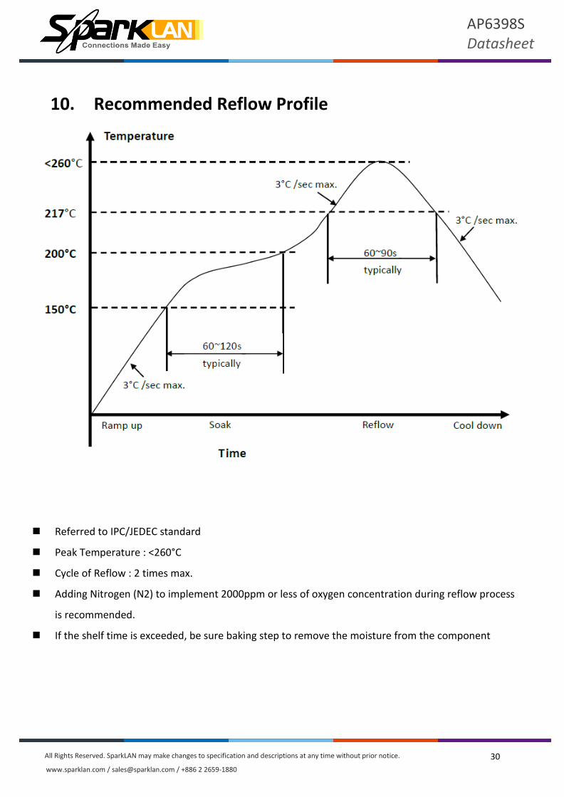
10. Recommended Reflow Profile
◼ Referred to IPC/JEDEC standard
◼ Peak Temperature : <260°C
◼ Cycle of Reflow : 2 times max.
◼ Adding Nitrogen (N2) to implement 2000ppm or less of oxygen concentration during reflow process
is recommended.
◼ If the shelf time is exceeded, be sure baking step to remove the moisture from the component
31
AP6398S
Datasheet
All Rights Reserved. SparkLAN may make changes to specification and descriptions at any time without prior notice.
www.sparklan.com / [email protected] / +886 2 2659-1880
10.1 Caution for SMT Preparation
Moisture Sensitivity Level: 4
1. Calculated shelf life in sealed bag: 12 months at <40℃ and <90% relative humidity (RH).
2. Peak package body temperature: 250℃.
3. After bag was opened, devices that will be subjected to reflow solder or other high temperature process must be
a) Mounted within: 72 hours of factory conditions <30℃/60%RH or
b) Stored per J-STD-033
4. Devices require bake before mounting, if:
a) Humidity Indicator Card reads> 10% for level 2a - 5a devices or >60% for level 2 devices when
read at 23+5℃
b) 3a or 3b are not met.
5. If baking is required, refer to IPC/JEDEC J-STD-033 for bake procedure.
32
AP6398S
Datasheet
All Rights Reserved. SparkLAN may make changes to specification and descriptions at any time without prior notice.
www.sparklan.com / [email protected] / +886 2 2659-1880
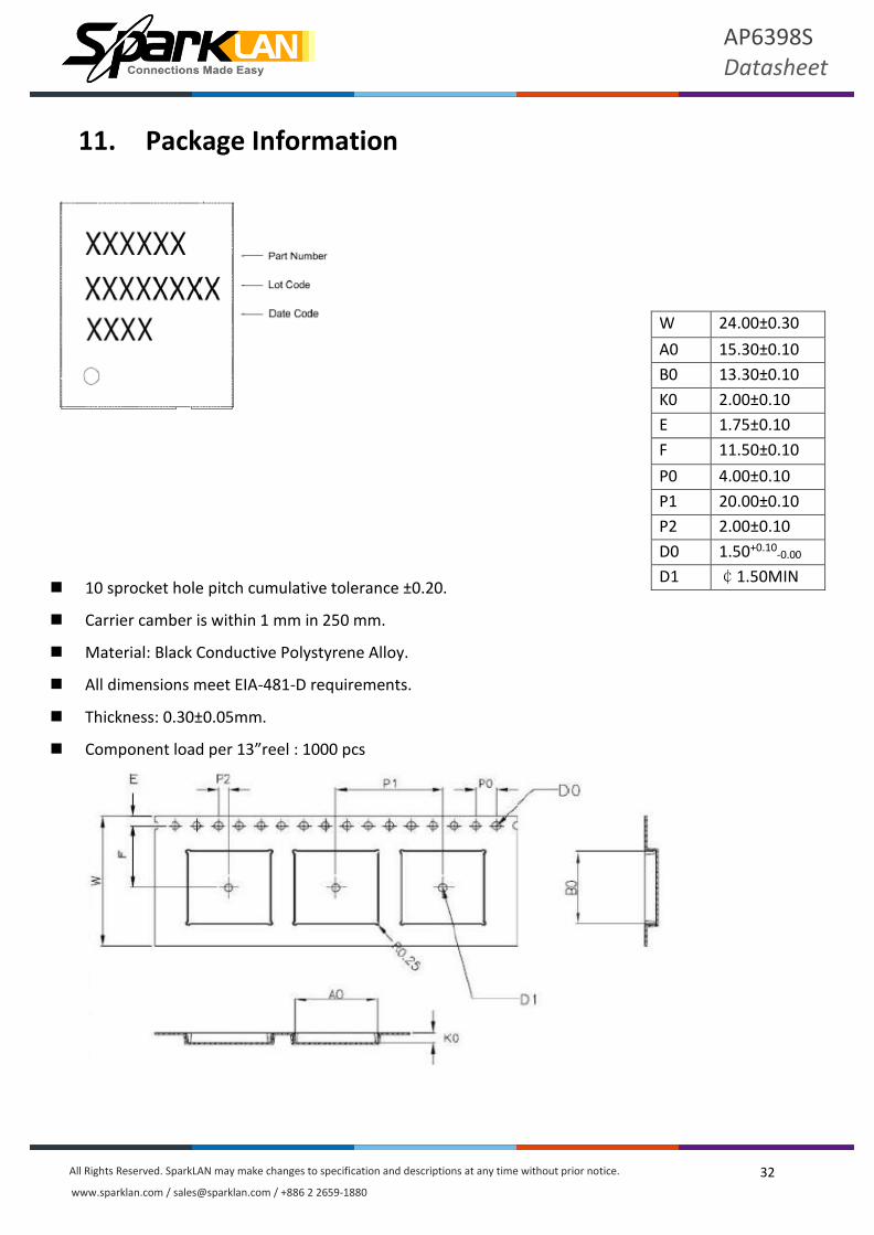
11. Package Information
◼ 10 sprocket hole pitch cumulative tolerance ±0.20.
◼ Carrier camber is within 1 mm in 250 mm.
◼ Material: Black Conductive Polystyrene Alloy.
◼ All dimensions meet EIA-481-D requirements.
◼ Thickness: 0.30±0.05mm.
◼ Component load per 13”reel : 1000 pcs
W 24.00±0.30
A0 15.30±0.10
B0 13.30±0.10
K0 2.00±0.10
E 1.75±0.10
F 11.50±0.10
P0 4.00±0.10
P1 20.00±0.10
P2 2.00±0.10
D0 1.50+0.10-0.00
D1 ¢1.50MIN

33
AP6398S
Datasheet
All Rights Reserved. SparkLAN may make changes to specification and descriptions at any time without prior notice.
www.sparklan.com / [email protected] / +886 2 2659-1880
Label B: MSL caution / Storage Condition
Label A: Anti-static and humidity notice Label C: Inner box label

34
AP6398S
Datasheet
All Rights Reserved. SparkLAN may make changes to specification and descriptions at any time without prior notice.
www.sparklan.com / [email protected] / +886 2 2659-1880
Note: 1 tape reel = 1 box = 1,000pcs
1 Carton = 5 box = 5,000pcs
12. Order Information
Product Name Part Number Description
AP6398S R9701820002 11ac/a/b/g/n 2T2R WiFi + BT5.0 Combo Sip Module
Label C: Inner box label
Label D: Carton box label