Embed Size (px)
Citation preview
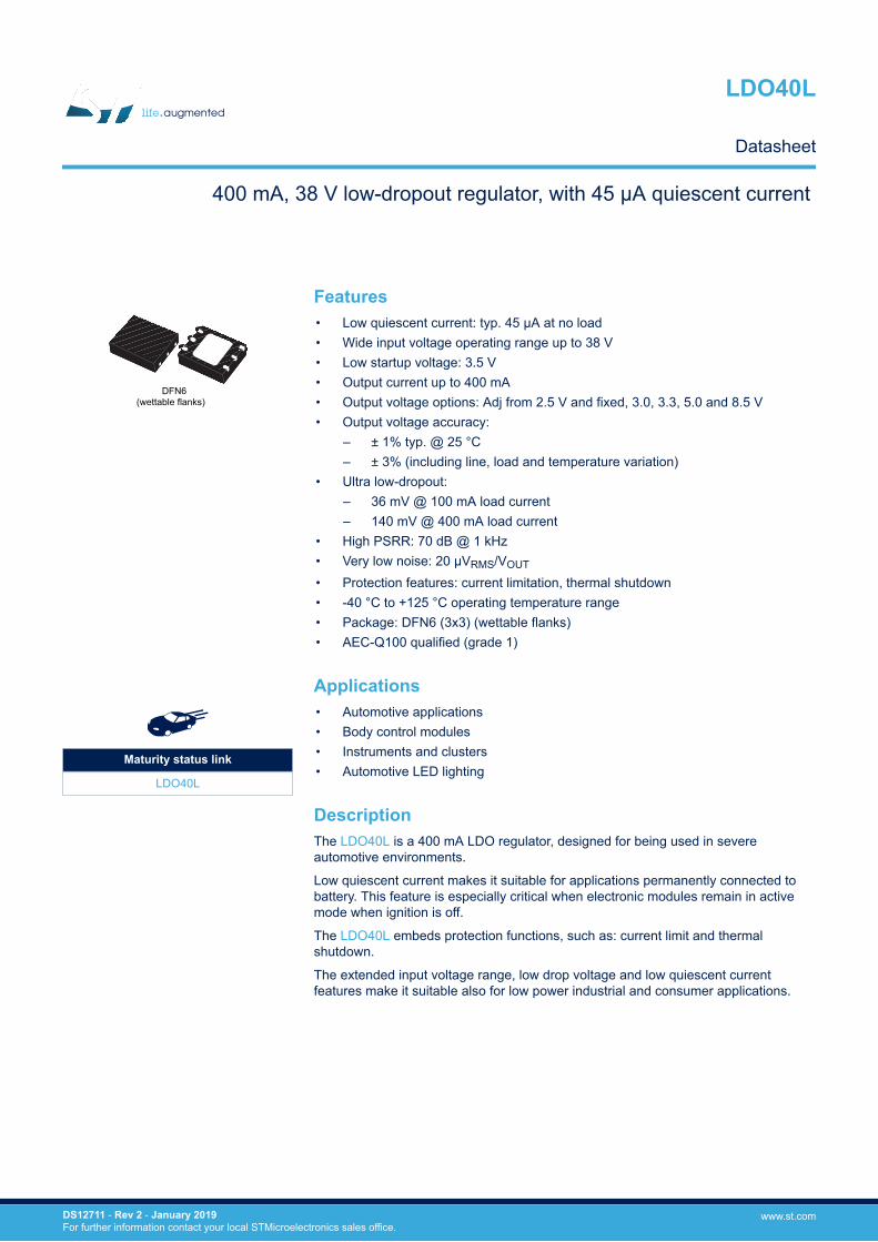
DFN6(wettable flanks)
Features• Low quiescent current: typ. 45 µA at no load• Wide input voltage operating range up to 38 V• Low startup voltage: 3.5 V• Output current up to 400 mA• Output voltage options: Adj from 2.5 V and fixed, 3.0, 3.3, 5.0 and 8.5 V• Output voltage accuracy:
– ± 1% typ. @ 25 °C– ± 3% (including line, load and temperature variation)
• Ultra low-dropout:– 36 mV @ 100 mA load current– 140 mV @ 400 mA load current
• High PSRR: 70 dB @ 1 kHz• Very low noise: 20 µVRMS/VOUT
• Protection features: current limitation, thermal shutdown• -40 °C to +125 °C operating temperature range• Package: DFN6 (3x3) (wettable flanks)• AEC-Q100 qualified (grade 1)
Applications• Automotive applications• Body control modules• Instruments and clusters• Automotive LED lighting
DescriptionThe LDO40L is a 400 mA LDO regulator, designed for being used in severeautomotive environments.
Low quiescent current makes it suitable for applications permanently connected tobattery. This feature is especially critical when electronic modules remain in activemode when ignition is off.
The LDO40L embeds protection functions, such as: current limit and thermalshutdown.
The extended input voltage range, low drop voltage and low quiescent currentfeatures make it suitable also for low power industrial and consumer applications.
Maturity status link
LDO40L
400 mA, 38 V low-dropout regulator, with 45 μA quiescent current
LDO40L
Datasheet
DS12711 - Rev 2 - January 2019For further information contact your local STMicroelectronics sales office.
www.st.com
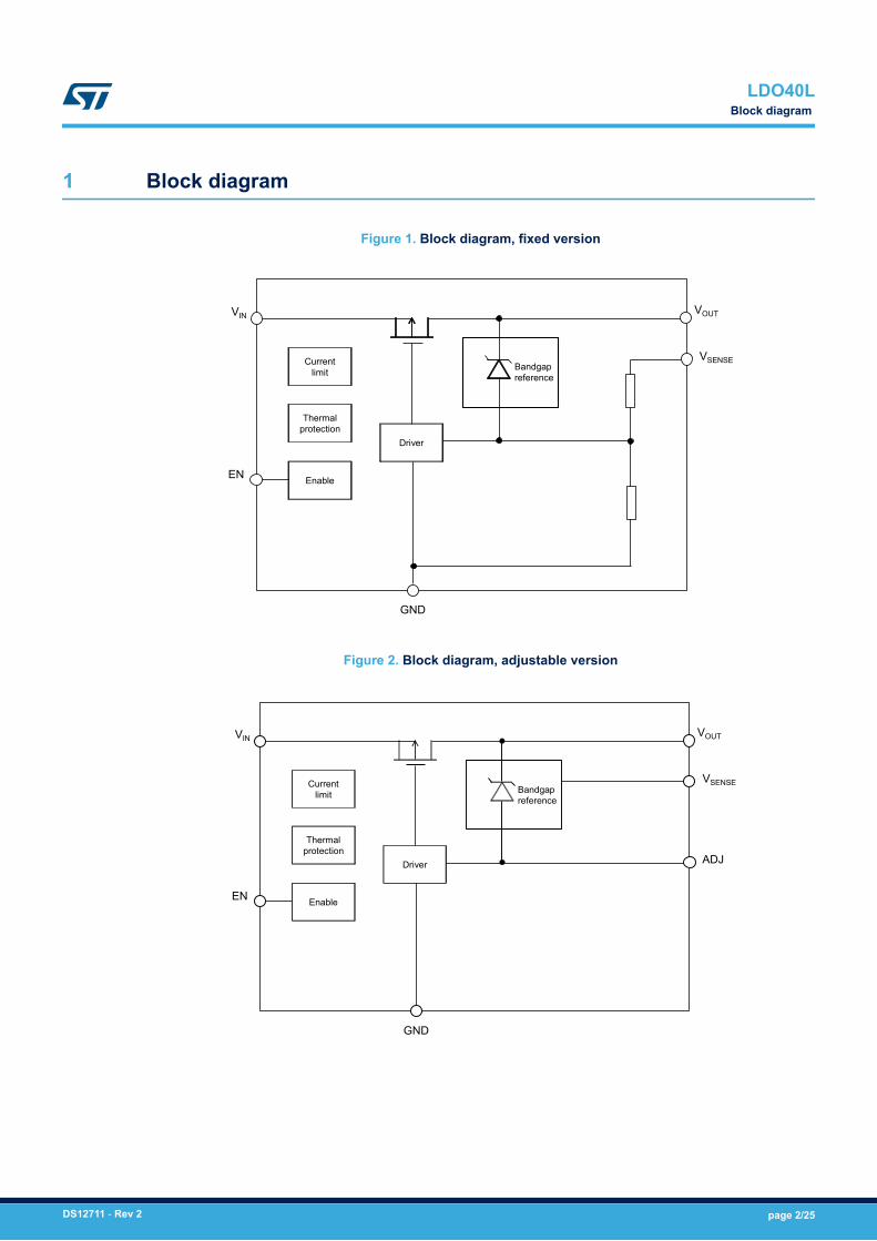
1 Block diagram
Figure 1. Block diagram, fixed version
VI N VO U T
C u rr en t li m i t
T he r m a lp r o t e c t i o n
D r i v e rE nab l e
VSE NS E
E N
B andga pr e f e r en c e
G ND
Figure 2. Block diagram, adjustable version
VI N
G ND
VO U T
C u rr en t li m i t
T he r m a lp r o t e c t i o n
D r i v e r
E nab l e
VSE NS E
E N
A DJ
B andga pr e f e r en c e
LDO40LBlock diagram
DS12711 - Rev 2 page 2/25
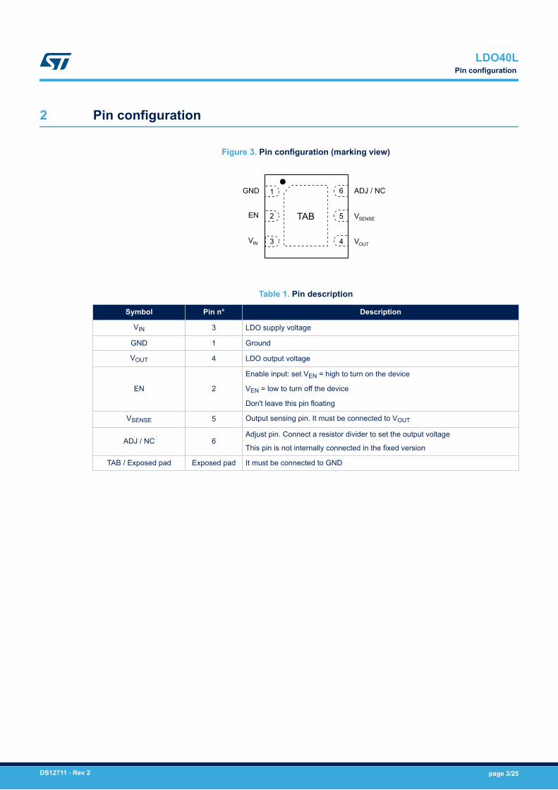
2 Pin configuration
Figure 3. Pin configuration (marking view)
1
2
3
6
5
4
TAB
ADJ / NC
V
V
GND
EN
VIN OUT
SENSE
Table 1. Pin description
Symbol Pin n° Description
VIN 3 LDO supply voltage
GND 1 Ground
VOUT 4 LDO output voltage
EN 2
Enable input: set VEN = high to turn on the device
VEN = low to turn off the device
Don't leave this pin floating
VSENSE 5 Output sensing pin. It must be connected to VOUT
ADJ / NC 6Adjust pin. Connect a resistor divider to set the output voltage
This pin is not internally connected in the fixed version
TAB / Exposed pad Exposed pad It must be connected to GND
LDO40LPin configuration
DS12711 - Rev 2 page 3/25

3 Typical application diagram
Figure 4. Typical application diagram (fixed versions)
VC C
G N D
VI N
E N
CI N
VO U T
VO U T
CO U T
L D O 40 LO FF
O N VSE N SE
Figure 5. Typical application diagram (adjustable versions)
VC C
G N D
VI NE N
CI N
VO U TVO U T
CO U TLDO 40 LO FF
O N VSE N SER1
R2
A D J
LDO40LTypical application diagram
DS12711 - Rev 2 page 4/25
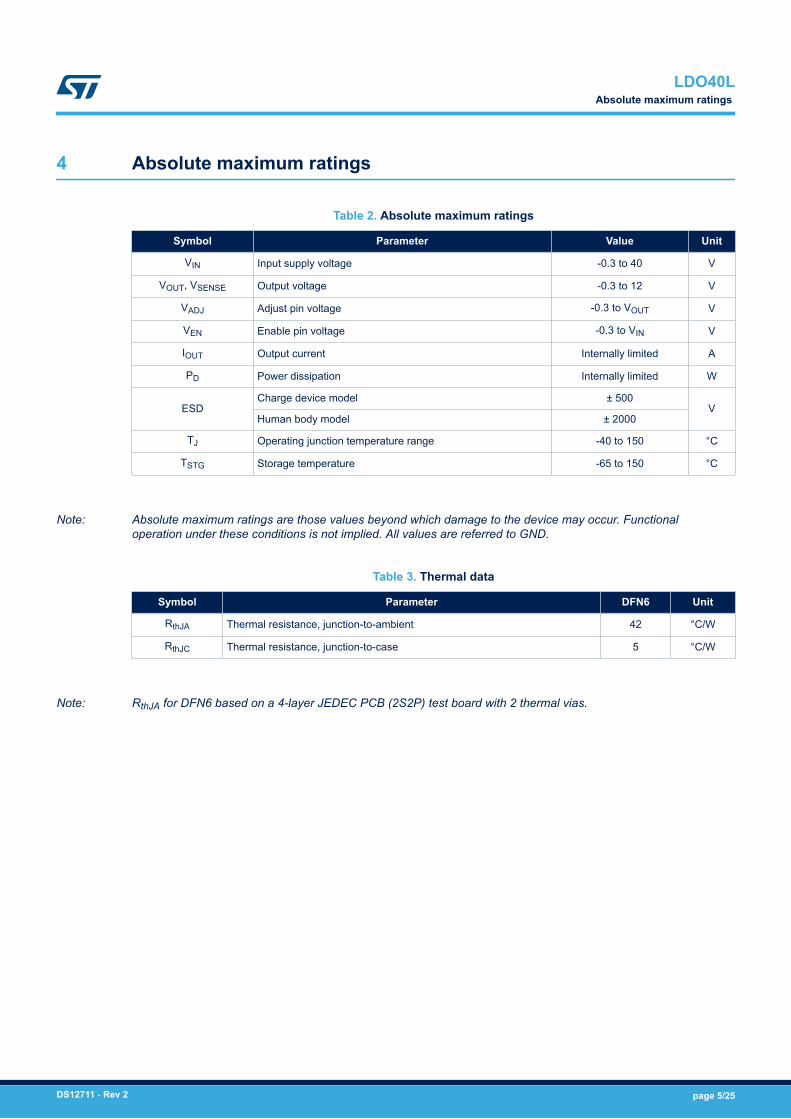
4 Absolute maximum ratings
Table 2. Absolute maximum ratings
Symbol Parameter Value Unit
VIN Input supply voltage -0.3 to 40 V
VOUT, VSENSE Output voltage -0.3 to 12 V
VADJ Adjust pin voltage -0.3 to VOUT V
VEN Enable pin voltage -0.3 to VIN V
IOUT Output current Internally limited A
PD Power dissipation Internally limited W
ESDCharge device model ± 500
VHuman body model ± 2000
TJ Operating junction temperature range -40 to 150 °C
TSTG Storage temperature -65 to 150 °C
Note: Absolute maximum ratings are those values beyond which damage to the device may occur. Functionaloperation under these conditions is not implied. All values are referred to GND.
Table 3. Thermal data
Symbol Parameter DFN6 Unit
RthJA Thermal resistance, junction-to-ambient 42 °C/W
RthJC Thermal resistance, junction-to-case 5 °C/W
Note: RthJA for DFN6 based on a 4-layer JEDEC PCB (2S2P) test board with 2 thermal vias.
LDO40LAbsolute maximum ratings
DS12711 - Rev 2 page 5/25
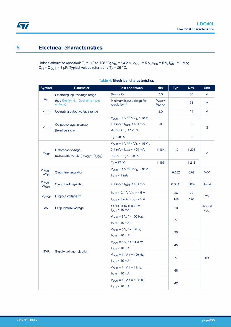
5 Electrical characteristics
Unless otherwise specified: TJ = -40 to 125 °C; VIN = 13.2 V, VOUT = 5 V, VEN = 5 V, IOUT = 1 mA;CIN = COUT = 1 µF; Typical values referred to TA = 25 °C.
Table 4. Electrical characteristics
Symbol Parameter Test conditions Min. Typ. Max. Unit
VIN
Operating input voltage range
(see Section 6.1 Operating inputvoltage)
Device On 3.5 38 V
Minimum input voltage forregulation (1)
VOUT+VDROP
38 V
VOUT Operating output voltage range 2.5 11 V
VOUTOutput voltage accuracy
(fixed version)
VOUT + 1 V (2) < VIN < 18 V,
0.1 mA < IOUT < 400 mA,
-40 °C < TJ < 125 °C
-3 3%
TJ = 25 °C -1 1
VREFReference voltage
(adjustable version) (VOUT - VADJ)
VOUT + 1 V (2) < VIN < 18 V ,
0.1 mA < IOUT < 400 mA,
-40 °C < TJ < 125 °C
1.164 1.2 1.236V
TJ = 25 °C 1.188 1.212
ΔVOUT/ΔVIN
Static line regulationVOUT + 1 V (2) < VIN < 18 V;
IOUT = 1 mA0.002 0.02 %/V
ΔVOUT/ΔIOUT
Static load regulation 0.1 mA < IOUT < 400 mA 0.0001 0.002 %/mA
VDROP Dropout voltage (3)IOUT = 0.1 A; VOUT = 5 V 36 70
mVIOUT = 0.4 A; VOUT = 5 V 140 270
eN Output noise voltage f = 10 Hz to 100 kHz;IOUT = 10 mA 20
µVRMS/VOUT
SVR Supply voltage rejection
VOUT = 5 V, f = 100 Hz;
IOUT = 10 mA77
VOUT = 5 V, f = 1 kHz;
IOUT = 10 mA70
dB
VOUT = 5 V, f = 10 kHz;
IOUT = 10 mA45
VOUT = 11 V, f = 100 Hz;
IOUT = 10 mA77
VOUT = 11 V, f = 1 kHz;
IOUT = 10 mA68
VOUT = 11 V, f = 10 kHz;
IOUT = 10 mA42
LDO40LElectrical characteristics
DS12711 - Rev 2 page 6/25
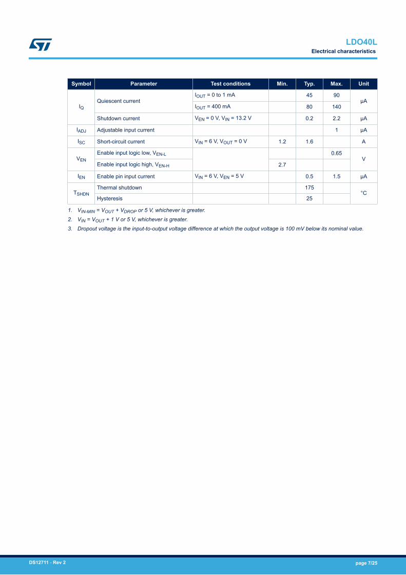
Symbol Parameter Test conditions Min. Typ. Max. Unit
IQQuiescent current
IOUT = 0 to 1 mA 45 90µA
IOUT = 400 mA 80 140
Shutdown current VEN = 0 V, VIN = 13.2 V 0.2 2.2 µA
IADJ Adjustable input current 1 µA
ISC Short-circuit current VIN = 6 V, VOUT = 0 V 1.2 1.6 A
VENEnable input logic low, VEN-L 0.65
VEnable input logic high, VEN-H 2.7
IEN Enable pin input current VIN = 6 V, VEN = 5 V 0.5 1.5 µA
TSHDNThermal shutdown 175
°CHysteresis 25
1. VIN-MIN = VOUT + VDROP or 5 V, whichever is greater.
2. VIN = VOUT + 1 V or 5 V, whichever is greater.
3. Dropout voltage is the input-to-output voltage difference at which the output voltage is 100 mV below its nominal value.
LDO40LElectrical characteristics
DS12711 - Rev 2 page 7/25

6 Application information
6.1 Operating input voltageThe LDO40L is a low-dropout linear voltage regulator equipped with a low-RDS-(on) P-channel MOSFET used as apass-element. The device internal circuits are able to start with an input voltage as low as 3.5 V, whatever is thenominal output voltage (see Figure 22. Output voltage vs. input voltage (no load). Defined the desired outputvoltage VOUT-NOM, the minimum input voltage VIN-MIN needed to fully bias the pass-element, isVIN-MIN = VOUT-NOM + VDROP. This allows to exit the dropout condition and achieve output voltage regulation.The full regulation performance guaranteed by Section 5 Electrical characteristics in terms of output accuracy andtolerance versus line and load changes is achieved for the highest input voltage among VIN-MIN = VOUT-NOM + 1 Vand VIN-MIN = 5 V .At input voltages lower than VIN-MIN = (VOUT-NOM + VDROP) the regulator enters dropout condition, regulation isnot guaranteed and the output voltage tracks the input except for a voltage depending on the load current (IOUT)and the pass-element resistance (see Figure 22. Output voltage vs. input voltage (no load). This tracking behaviorcan be useful during cold crank conditions.
6.2 Output voltage adjustmentThe LDO40LY is available in fixed and adjustable output voltage versions. The latter option is usually chosenwhen the output voltage has to be set to non-standard values. In the adjustable version, the output voltage can beset from 2.5 V up to 11 V, by connecting a resistor divider between the ADJ pin and the output.The architecture of the LDO40LY features a precise bandgap reference, which generates a fixed voltage VREF =1.2 V between VOUT and ADJ terminals (refer to Figure 2. Block diagram, adjustable version and Figure 5. Typicalapplication diagram (adjustable versions) ). When the R1-R2 resistor divider is connected, a fixed current isgenerated through the divider. Since the contribution of current sourced by the ADJ pin is negligible (few tens ofnA), the resulting output voltage is obtained by using the following equation:VOUT = VREF 1 + R2/R1 , witℎ VREF = 1.2V typ. (1)
In order to guarantee a correct regulation, the resistor divider must be calculated for an output voltage of min.2.5 V.
6.3 Output voltage sense pinIn the DFN6 package on pin 5, an additional VSENSE connection is available. This pin must not be left floating,since it is necessary for a correct sensing of the output voltage. It can be either connected to the load in a remote-sensing configuration, or directly shorted to the VOUT pin (pin 4, refer to Figure 4. Typical application diagram(fixed versions) and Figure 5. Typical application diagram (adjustable versions)).
6.4 Protection featuresThe device is self-protected from short-circuits and overtemperature events.In case of strong overload or short-circuit on the output, the output current is limited to a value of typically 1.5 Aand kept constant even when the load impedance is zero. If the overload persists, the temperature on the internaldie rises, until the thermal protection is triggered, which happens when the junction temperature reaches 175 °C.The device is subsequently shut down. As soon as the junction temperature falls again below 150 °C the devicere-starts.Even if the above described protections are able to keep the device safe in the worst cases, a correct thermaldesign of the application is recommended, according to the operating ambient temperature and the maximumpower dissipation allowed by the chosen package. In order to calculate the maximum power that the device candissipate, keeping the junction temperature below TJ-OP = 125 °C, the following formula is used:PDMAX = 125− TAMB / RTHJ − A (2)
The power dissipation on the device is calculated as PD = (VIN - VOUT) x IOUT.
LDO40LApplication information
DS12711 - Rev 2 page 8/25
6.5 Enable pinThe enable function allows the LDO output to be enabled/disabled. The regulator is turned on in case the pin ENis connected to a voltage higher than VEN-H, the LDO can be turned off if the voltage on EN pin is lower thanVEN-L.No internal pull-up / pull-down is present on the EN pin, therefore it must not be left floating in the application.
6.6 Input and output capacitorsThe LDO40LY requires external capacitors to ensure the regulator control loop stability.A capacitor with a minimum value of 1 μF is required on at the input port of the LDO40LY.This capacitor must be located as close as possible to the input pin of the device and returned to a clean analogground. Good quality ceramic capacitors are suggested.The device control loop is designed to be stable with good quality ceramic capacitors (such as: X5R/X7R types)with a minimum capacitance of 1 μF and equivalent series resistance in the [5 mΩ – 12 Ω] range. There is noupper limit to the output capacitance. Figure 27. Stability plan shows the stability plan tested on real capacitors,up to 10 µF. A value of 4.7 μF is suitable for the majority of applications, improving dynamic response andminimizing the risk of ringing and oscillations. It is important to highlight that the output capacitor must maintain itscapacitance and ESR in the stable region over the full operating temperature, load and input voltage ranges, toassure stability. Therefore, capacitance and ESR variations must be taken into account in the design phase toensure the device works in the expected stability region. There is no maximum limit to the output capacitance,provided that the above conditions are respected.
LDO40LEnable pin
DS12711 - Rev 2 page 9/25

7 Typical characteristics
The following plots are referred to the typical application circuit with CIN = COUT = 1 μF and TA = 25 °C unlessotherwise noted.
Figure 6. Output voltage vs. temperature (VIN = 6 V,VOUT = adjusted to 5 V)
4 . 904 . 924 . 944 . 964 . 985 . 005 . 025 . 045 . 065 . 085 . 10
-50 -25 0 25 50 75 100 125 150
VO U
T[ V
]
Temperature [°C]
I o u t = 10 0 µ AI o u t = 40 0 m AI o u t = 1 m A
Figure 7. Output voltage vs. temperature (VIN = 13.2 V,VOUT adjusted to 5 V)
4 . 904 . 924 . 944 . 964 . 985 . 005 . 025 . 045 . 065 . 085 . 10
-50 -25 0 25 50 75 100 125 150
VO U
T[ V
]
Temperature [°C]
I o u t = 10 0 µ AI o u t = 40 0 m AI o u t = 1 m A
Figure 8. Output voltage vs. temperature (VIN = 18 V,VOUT = adjusted to 5 V)
4 . 904 . 924 . 944 . 964 . 985 . 005 . 025 . 045 . 065 . 085 . 10
-50 -25 0 25 50 75 100 125 150
VO U
T[ V
]
Temperature [°C]
I o u t = 10 0 µ AI o u t = 40 0 m AI o u t = 1 m A
Figure 9. Output voltage vs. temperature (VIN = 4.3 V,VOUT = 3.3 V)
4 . 904 . 924 . 944 . 964 . 985 . 005 . 025 . 045 . 065 . 085 . 10
-50 -25 0 25 50 75 100 125 150
VO U
T[ V
]
Temperature [°C]
I o u t = 10 0 µ AI o u t = 40 0 m AI o u t = 1 m A
LDO40LTypical characteristics
DS12711 - Rev 2 page 10/25

Figure 10. Output voltage vs. temperature (VIN = 13.2 V,VOUT = 3.3 V)
3 . 203 . 223 . 243 . 263 . 283 . 303 . 323 . 343 . 363 . 383 . 40
-50 -25 0 25 50 75 100 125 150
VO U
T[ V
]
Temperature [°C]
I o ut = 10 0 µ AI o ut = 40 0 m AI o ut = 1 m A
Figure 11. Output voltage vs. temperature (VIN = 18 V,VOUT = 3.3 V)
3 . 203 . 223 . 243 . 263 . 283 . 303 . 323 . 343 . 363 . 383 . 40
-50 -25 0 25 50 75 100 125 150
VO U
T[ V
]
Temperature [°C]
I o ut = 10 0 µ AI o ut = 40 0 m AI o ut = 1 m A
Figure 12. Reference voltage vs. temperature (VIN = 6 V,VOUT = adjusted to 5 V)
1 . 12
1 . 14
1 . 16
1 . 18
1 . 20
1 . 22
1 . 24
1 . 26
1 . 28
-50 -25 0 25 50 75 100 125 150
VRE F
[ V]
Temperature [°C]
I o u t = 10 0 µ AI o u t = 40 0 m A
Figure 13. Reference voltage vs. temperature (VIN = 18 V,VOUT = adjusted to 5 V)
1 . 12
1 . 14
1 . 16
1 . 18
1 . 20
1 . 22
1 . 24
1 . 26
1 . 28
-50 -25 0 25 50 75 100 125 150
VRE F
[ V]
Temperature [°C]
I o u t = 10 0 µ AI o u t = 40 0 m A
Figure 14. Line regulation vs. temperature
-0 . 003
-0 . 002
-0 . 001
0 . 000
0 . 001
0 . 002
0 . 003
-50 -25 0 25 50 75 100 125 150
Line
regu
latio
n[ %
/ V]
Temperature [°C]
VI N= 6 to18 V, VO U T = 5 V
Figure 15. Load regulation vs. temperature
-0 . 0010
-0 . 0005
0 . 0000
0 . 0005
0 . 0010
-50 -25 0 25 50 75 100 125 150
Load
regu
latio
n[ %
/ m A]
Temperature [°C]
VI N = 6 V , VO U T = 5 V , IO U T = 100 µ A t o 400 m A
LDO40LTypical characteristics
DS12711 - Rev 2 page 11/25

Figure 16. Dropout voltage vs. temperature
0 . 000
0 . 050
0 . 100
0 . 150
0 . 200
0 . 250
-50 -25 0 25 50 75 100 125 150
Dro
pout
Vol
tage
[ V]
Temperature [°C]
VO U T = 5 V
I o u t = 10 0 m AI o u t = 40 0 m A
Figure 17. Short-circuit current vs. temperature
0 . 8
1 . 0
1 . 2
1 . 4
1 . 6
1 . 8
2 . 0
-50 -25 0 25 50 75 100 125 150
Shor
t-circ
uit c
urre
nt [A
]
Temperature [°C]
Figure 18. Quiescent current vs. temperature
0 . 00
20 . 00
40 . 00
60 . 00
80 . 00
100 . 00
120 . 00
-50 -25 0 25 50 75 100 125 150
I Q[ µ
A]
Temperature [°C]
VI N = 13.2 V
I o u t = 0I o u t = 1 m AI o u t = 40 0 m A
Figure 19. Off-state current vs. temperature
0 . 000 . 200 . 400 . 600 . 801 . 001 . 201 . 401 . 601 . 802 . 00
-50 -25 0 25 50 75 100 125 150
I q-O
f f[ µ
A]
T e m pera t ure [°C ]
VI N = 13 . 2 V , VE N = 0 V
Figure 20. Enable thresholds vs. temperature
0 . 00
0 . 50
1 . 00
1 . 50
2 . 00
2 . 50
3 . 00
-50 -25 0 25 50 75 100 125 150
Enab
le t h
re s h
olds
[ V]
T e m pera t ure [°C ]
IO U T = 1 m A
Figure 21. Enable input current vs. temperature
0 . 000 . 100 . 200 . 300 . 400 . 500 . 600 . 700 . 800 . 901 . 00
-50 -25 0 25 50 75 100 125 150
I EN
[ µ A]
T e m pera t ure [°C ]
VI N = 5 V , VE N = 5 V
LDO40LTypical characteristics
DS12711 - Rev 2 page 12/25

Figure 22. Output voltage vs. input voltage (no load)
0.000.501.001.502.002.503.003.504.004.505.00
0 0.5 1 1.5 2 2.5 3 3.5 4 4.5 5
V OU
T[V
]
VIN [V]
VIN = VEN = from 0 V to 5 V, CIN = COUT = 1 µF, VOUT = 3.3 V, No Load
T=25°CT=125°CT=-40°C
Figure 23. Output voltage vs. input voltage (IOUT = 1 mA)
0.000.501.001.502.002.503.003.504.004.505.00
0 0.5 1 1.5 2 2.5 3 3.5 4 4.5 5
V OU
T[V
]
VIN [V]
VIN = VEN = from 0 V to 5 V, CIN = COUT = 1 µF, VOUT = 3.3 V, IOUT = 1 mA
T=25°CT=125°CT=-40°C
Figure 24. Output voltage vs. input voltage(IOUT = 100 mA)
0.000.501.001.502.002.503.003.504.004.505.00
0 0.5 1 1.5 2 2.5 3 3.5 4 4.5 5
V OU
T[V
]
VIN [V]
VIN = VEN = from 0 V to 5 V, CIN = COUT = 1 µF, VOUT = 3.3 V, IOUT = 100 mA
T=25°CT=125°CT=-40°C
Figure 25. Output voltage vs. input voltage(IOUT = 400 mA)
0.000.501.001.502.002.503.003.504.004.505.00
0 0.5 1 1.5 2 2.5 3 3.5 4 4.5 5
V OU
T[V
]
VIN [V]
VIN = VEN = from 0 V to 5 V, CIN = COUT = 1 µF, VOUT = 3.3 V, IOUT = 400 mA
T=25°CT=125°CT=-40°C
Figure 26. Quiescent current vs. input voltage
020406080
100120140160180200
0 5 10 15 20 25 30 35 40
I q[µ
A]
VIN [V]
VIN = VEN = from 0 V to 38 V, VOUT = 5 V
No LoadIout=1mA
Figure 27. Stability plan
0.001
0.010
0.100
1.000
10.000
1 2.2 4.7 10
ESR
@10
0 kH
z [Ω
]
COUT [µF]
VIN = VIN_MIN to 38 V, IOUT = 1 mA to 400 mA , CIN = 1 µF
Untested area
Stability area
LDO40LTypical characteristics
DS12711 - Rev 2 page 13/25

Figure 28. PSRR vs. frequency
0
5
10
15
20
25
30
35
40
45
50
55
60
65
70
75
80
85
0.01 0.10 1.00 10.00 100.00 1,000.00 10,000.00
PSR
R (d
B)
Frequency (kHz)
Vout=5V Iload=10mA
Vout=11V Iload=10mA
Figure 29. Output noise spectrum
0.001
0.010
0.100
1.000
10.000
0.01 0.1 1 10 100 1000
Out
put N
oise
Den
sity
:
[µ
V/s
qrt(H
z)]
Frequency: f [kHz]
VIN = 13.2 VVOUT = 5 V (ADJ) CIN = 1 µFCOUT = 1 µFIOUT = 10 mA
Figure 30. Line transient (tr = tf = 1 µs) Figure 31. Line transient (tr = tf = 10 µs)
Figure 32. Load transient (0.1 mA to 100 mA, tr = tf = 1 µs)Figure 33. Load transient (0.1 mA to 100 mA,
tr = tf = 10 µs)
LDO40LTypical characteristics
DS12711 - Rev 2 page 14/25
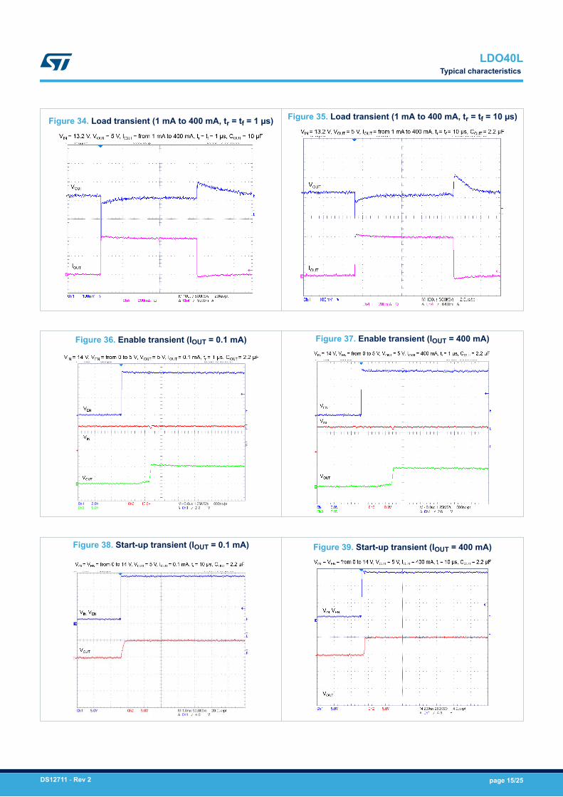
Figure 34. Load transient (1 mA to 400 mA, tr = tf = 1 µs) Figure 35. Load transient (1 mA to 400 mA, tr = tf = 10 µs)
Figure 36. Enable transient (IOUT = 0.1 mA) Figure 37. Enable transient (IOUT = 400 mA)
Figure 38. Start-up transient (IOUT = 0.1 mA) Figure 39. Start-up transient (IOUT = 400 mA)
LDO40LTypical characteristics
DS12711 - Rev 2 page 15/25

8 Package information
In order to meet environmental requirements, ST offers these devices in different grades of ECOPACK®
packages, depending on their level of environmental compliance. ECOPACK® specifications, grade definitionsand product status are available at: www.st.com. ECOPACK® is an ST trademark.
8.1 DFN6 (3x3) package information
Figure 40. DFN6 (3x3) package outline
BOTTOM VIEW
TOP VIEW
DETAIL A
LDO40LPackage information
DS12711 - Rev 2 page 16/25

Table 5. DFN6 (3x3) mechanical data
Dim.mm
Min. Typ. Max.
A 0.80 0.85 0.90
A1 0.00 0.05
b 0.20 0.25 0.30
D 2.95 3.00 3.05
D2 2.30 2.40 2.50
e 0.95 BSC
E 2.95 3.00 3.05
E2 1.50 1.60 1.70
L 0.30 0.40 0.50
K 0.30 Ref.
aaa 0.10
bbb 0.10
ccc 0.10
ddd 0.10
Figure 41. DFN6 (3x3) recommended footprint (dimensions are in mm)
LDO40LDFN6 (3x3) package information
DS12711 - Rev 2 page 17/25
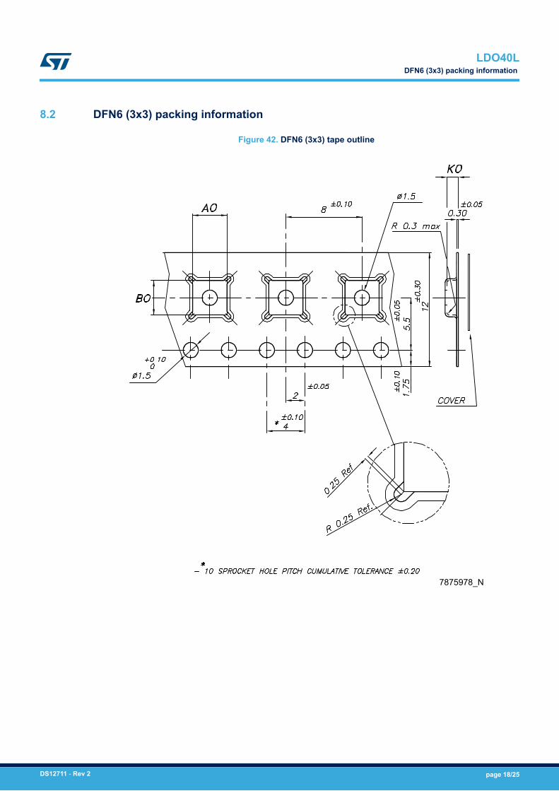
8.2 DFN6 (3x3) packing information
Figure 42. DFN6 (3x3) tape outline
7875978_N
LDO40LDFN6 (3x3) packing information
DS12711 - Rev 2 page 18/25

Figure 43. DFN6 (3x3) reel outline
7875978_N
Table 6. DFN6 (3x3) tape and reel mechanical data
Dim.mm
Min. Typ. Max.
A0 3.20 3.30 3.40
B0 3.20 3.30 3.40
K0 1 1.10 1.20
LDO40LDFN6 (3x3) packing information
DS12711 - Rev 2 page 19/25
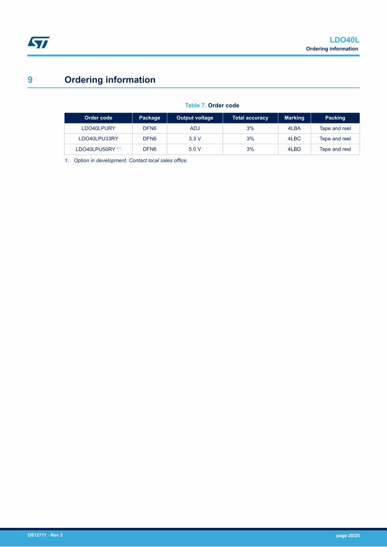
9 Ordering information
Table 7. Order code
Order code Package Output voltage Total accuracy Marking Packing
LDO40LPURY DFN6 ADJ 3% 4LBA Tape and reel
LDO40LPU33RY DFN6 3.3 V 3% 4LBC Tape and reel
LDO40LPU50RY (1) DFN6 5.0 V 3% 4LBD Tape and reel
1. Option in development. Contact local sales office.
LDO40LOrdering information
DS12711 - Rev 2 page 20/25
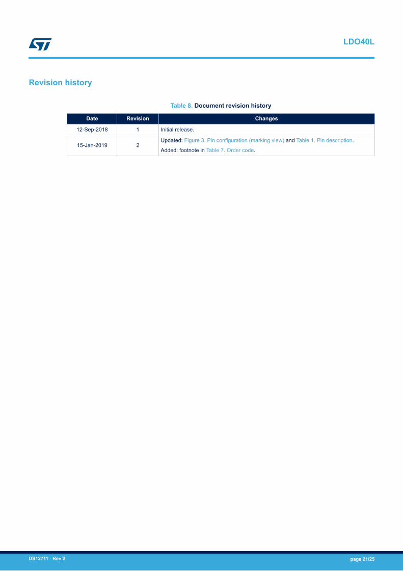
Revision history
Table 8. Document revision history
Date Revision Changes
12-Sep-2018 1 Initial release.
15-Jan-2019 2Updated: Figure 3. Pin configuration (marking view) and Table 1. Pin description.
Added: footnote in Table 7. Order code.
LDO40L
DS12711 - Rev 2 page 21/25
Contents
1 Block diagram . . . . . . . . . . . . . . . . . . . . . . . . . . . . . . . . . . . . . . . . . . . . . . . . . . . . . . . . . . . . . . . . . . . . .2
2 Pin configuration . . . . . . . . . . . . . . . . . . . . . . . . . . . . . . . . . . . . . . . . . . . . . . . . . . . . . . . . . . . . . . . . . .3
3 Typical application diagram. . . . . . . . . . . . . . . . . . . . . . . . . . . . . . . . . . . . . . . . . . . . . . . . . . . . . . . .4
4 Absolute maximum ratings . . . . . . . . . . . . . . . . . . . . . . . . . . . . . . . . . . . . . . . . . . . . . . . . . . . . . . . .5
5 Electrical characteristics. . . . . . . . . . . . . . . . . . . . . . . . . . . . . . . . . . . . . . . . . . . . . . . . . . . . . . . . . . .6
6 Application information. . . . . . . . . . . . . . . . . . . . . . . . . . . . . . . . . . . . . . . . . . . . . . . . . . . . . . . . . . . .8
6.1 Operating input voltage . . . . . . . . . . . . . . . . . . . . . . . . . . . . . . . . . . . . . . . . . . . . . . . . . . . . . . . . . 8
6.2 Output voltage adjustment . . . . . . . . . . . . . . . . . . . . . . . . . . . . . . . . . . . . . . . . . . . . . . . . . . . . . . . 8
6.3 Output voltage sense pin . . . . . . . . . . . . . . . . . . . . . . . . . . . . . . . . . . . . . . . . . . . . . . . . . . . . . . . . 8
6.4 Protection features . . . . . . . . . . . . . . . . . . . . . . . . . . . . . . . . . . . . . . . . . . . . . . . . . . . . . . . . . . . . . 8
6.5 Enable pin . . . . . . . . . . . . . . . . . . . . . . . . . . . . . . . . . . . . . . . . . . . . . . . . . . . . . . . . . . . . . . . . . . . . 8
6.6 Input and output capacitors . . . . . . . . . . . . . . . . . . . . . . . . . . . . . . . . . . . . . . . . . . . . . . . . . . . . . . 9
7 Typical characteristics . . . . . . . . . . . . . . . . . . . . . . . . . . . . . . . . . . . . . . . . . . . . . . . . . . . . . . . . . . . .10
8 Package information. . . . . . . . . . . . . . . . . . . . . . . . . . . . . . . . . . . . . . . . . . . . . . . . . . . . . . . . . . . . . .16
8.1 DFN6 (3x3) package information . . . . . . . . . . . . . . . . . . . . . . . . . . . . . . . . . . . . . . . . . . . . . . . . 16
8.2 DFN6 (3x3) tape and reel mechanical data . . . . . . . . . . . . . . . . . . . . . . . . . . . . . . . . . . . . . . . . 17
9 Ordering information . . . . . . . . . . . . . . . . . . . . . . . . . . . . . . . . . . . . . . . . . . . . . . . . . . . . . . . . . . . . .20
Revision history . . . . . . . . . . . . . . . . . . . . . . . . . . . . . . . . . . . . . . . . . . . . . . . . . . . . . . . . . . . . . . . . . . . . . . .21
LDO40LContents
DS12711 - Rev 2 page 22/25

List of tablesTable 1. Pin description. . . . . . . . . . . . . . . . . . . . . . . . . . . . . . . . . . . . . . . . . . . . . . . . . . . . . . . . . . . . . . . . . . . . . . 3Table 2. Absolute maximum ratings . . . . . . . . . . . . . . . . . . . . . . . . . . . . . . . . . . . . . . . . . . . . . . . . . . . . . . . . . . . . . 5Table 3. Thermal data. . . . . . . . . . . . . . . . . . . . . . . . . . . . . . . . . . . . . . . . . . . . . . . . . . . . . . . . . . . . . . . . . . . . . . . 5Table 4. Electrical characteristics . . . . . . . . . . . . . . . . . . . . . . . . . . . . . . . . . . . . . . . . . . . . . . . . . . . . . . . . . . . . . . . 6Table 5. DFN6 (3x3) mechanical data . . . . . . . . . . . . . . . . . . . . . . . . . . . . . . . . . . . . . . . . . . . . . . . . . . . . . . . . . . . 17Table 6. DFN6 (3x3) tape and reel mechanical data . . . . . . . . . . . . . . . . . . . . . . . . . . . . . . . . . . . . . . . . . . . . . . . . . 19Table 7. Order code . . . . . . . . . . . . . . . . . . . . . . . . . . . . . . . . . . . . . . . . . . . . . . . . . . . . . . . . . . . . . . . . . . . . . . . 20Table 8. Document revision history . . . . . . . . . . . . . . . . . . . . . . . . . . . . . . . . . . . . . . . . . . . . . . . . . . . . . . . . . . . . . 21
LDO40LList of tables
DS12711 - Rev 2 page 23/25
List of figuresFigure 1. Block diagram, fixed version. . . . . . . . . . . . . . . . . . . . . . . . . . . . . . . . . . . . . . . . . . . . . . . . . . . . . . . . . . . 2Figure 2. Block diagram, adjustable version . . . . . . . . . . . . . . . . . . . . . . . . . . . . . . . . . . . . . . . . . . . . . . . . . . . . . . . 2Figure 3. Pin configuration (marking view) . . . . . . . . . . . . . . . . . . . . . . . . . . . . . . . . . . . . . . . . . . . . . . . . . . . . . . . . 3Figure 4. Typical application diagram (fixed versions) . . . . . . . . . . . . . . . . . . . . . . . . . . . . . . . . . . . . . . . . . . . . . . . . 4Figure 5. Typical application diagram (adjustable versions) . . . . . . . . . . . . . . . . . . . . . . . . . . . . . . . . . . . . . . . . . . . . 4Figure 6. Output voltage vs. temperature (VIN = 6 V, VOUT = adjusted to 5 V) . . . . . . . . . . . . . . . . . . . . . . . . . . . . . . . 10Figure 7. Output voltage vs. temperature (VIN = 13.2 V, VOUT adjusted to 5 V) . . . . . . . . . . . . . . . . . . . . . . . . . . . . . . 10Figure 8. Output voltage vs. temperature (VIN = 18 V, VOUT = adjusted to 5 V) . . . . . . . . . . . . . . . . . . . . . . . . . . . . . . 10Figure 9. Output voltage vs. temperature (VIN = 4.3 V, VOUT = 3.3 V) . . . . . . . . . . . . . . . . . . . . . . . . . . . . . . . . . . . . 10Figure 10. Output voltage vs. temperature (VIN = 13.2 V, VOUT = 3.3 V) . . . . . . . . . . . . . . . . . . . . . . . . . . . . . . . . . . . 11Figure 11. Output voltage vs. temperature (VIN = 18 V, VOUT = 3.3 V) . . . . . . . . . . . . . . . . . . . . . . . . . . . . . . . . . . . . . 11Figure 12. Reference voltage vs. temperature (VIN = 6 V, VOUT = adjusted to 5 V) . . . . . . . . . . . . . . . . . . . . . . . . . . . . 11Figure 13. Reference voltage vs. temperature (VIN = 18 V, VOUT = adjusted to 5 V) . . . . . . . . . . . . . . . . . . . . . . . . . . . 11Figure 14. Line regulation vs. temperature. . . . . . . . . . . . . . . . . . . . . . . . . . . . . . . . . . . . . . . . . . . . . . . . . . . . . . . . 11Figure 15. Load regulation vs. temperature . . . . . . . . . . . . . . . . . . . . . . . . . . . . . . . . . . . . . . . . . . . . . . . . . . . . . . . 11Figure 16. Dropout voltage vs. temperature . . . . . . . . . . . . . . . . . . . . . . . . . . . . . . . . . . . . . . . . . . . . . . . . . . . . . . . 12Figure 17. Short-circuit current vs. temperature . . . . . . . . . . . . . . . . . . . . . . . . . . . . . . . . . . . . . . . . . . . . . . . . . . . . 12Figure 18. Quiescent current vs. temperature. . . . . . . . . . . . . . . . . . . . . . . . . . . . . . . . . . . . . . . . . . . . . . . . . . . . . . 12Figure 19. Off-state current vs. temperature. . . . . . . . . . . . . . . . . . . . . . . . . . . . . . . . . . . . . . . . . . . . . . . . . . . . . . . 12Figure 20. Enable thresholds vs. temperature . . . . . . . . . . . . . . . . . . . . . . . . . . . . . . . . . . . . . . . . . . . . . . . . . . . . . 12Figure 21. Enable input current vs. temperature . . . . . . . . . . . . . . . . . . . . . . . . . . . . . . . . . . . . . . . . . . . . . . . . . . . . 12Figure 22. Output voltage vs. input voltage (no load). . . . . . . . . . . . . . . . . . . . . . . . . . . . . . . . . . . . . . . . . . . . . . . . . 13Figure 23. Output voltage vs. input voltage (IOUT = 1 mA) . . . . . . . . . . . . . . . . . . . . . . . . . . . . . . . . . . . . . . . . . . . . . 13Figure 24. Output voltage vs. input voltage (IOUT = 100 mA) . . . . . . . . . . . . . . . . . . . . . . . . . . . . . . . . . . . . . . . . . . . 13Figure 25. Output voltage vs. input voltage (IOUT = 400 mA) . . . . . . . . . . . . . . . . . . . . . . . . . . . . . . . . . . . . . . . . . . . 13Figure 26. Quiescent current vs. input voltage . . . . . . . . . . . . . . . . . . . . . . . . . . . . . . . . . . . . . . . . . . . . . . . . . . . . . 13Figure 27. Stability plan . . . . . . . . . . . . . . . . . . . . . . . . . . . . . . . . . . . . . . . . . . . . . . . . . . . . . . . . . . . . . . . . . . . . 13Figure 28. PSRR vs. frequency . . . . . . . . . . . . . . . . . . . . . . . . . . . . . . . . . . . . . . . . . . . . . . . . . . . . . . . . . . . . . . . 14Figure 29. Output noise spectrum. . . . . . . . . . . . . . . . . . . . . . . . . . . . . . . . . . . . . . . . . . . . . . . . . . . . . . . . . . . . . . 14Figure 30. Line transient (tr = tf = 1 µs) . . . . . . . . . . . . . . . . . . . . . . . . . . . . . . . . . . . . . . . . . . . . . . . . . . . . . . . . . . 14Figure 31. Line transient (tr = tf = 10 µs) . . . . . . . . . . . . . . . . . . . . . . . . . . . . . . . . . . . . . . . . . . . . . . . . . . . . . . . . . 14Figure 32. Load transient (0.1 mA to 100 mA, tr = tf = 1 µs) . . . . . . . . . . . . . . . . . . . . . . . . . . . . . . . . . . . . . . . . . . . . 14Figure 33. Load transient (0.1 mA to 100 mA, tr = tf = 10 µs) . . . . . . . . . . . . . . . . . . . . . . . . . . . . . . . . . . . . . . . . . . . 14Figure 34. Load transient (1 mA to 400 mA, tr = tf = 1 µs) . . . . . . . . . . . . . . . . . . . . . . . . . . . . . . . . . . . . . . . . . . . . . 15Figure 35. Load transient (1 mA to 400 mA, tr = tf = 10 µs) . . . . . . . . . . . . . . . . . . . . . . . . . . . . . . . . . . . . . . . . . . . . 15Figure 36. Enable transient (IOUT = 0.1 mA). . . . . . . . . . . . . . . . . . . . . . . . . . . . . . . . . . . . . . . . . . . . . . . . . . . . . . . 15Figure 37. Enable transient (IOUT = 400 mA) . . . . . . . . . . . . . . . . . . . . . . . . . . . . . . . . . . . . . . . . . . . . . . . . . . . . . . 15Figure 38. Start-up transient (IOUT = 0.1 mA) . . . . . . . . . . . . . . . . . . . . . . . . . . . . . . . . . . . . . . . . . . . . . . . . . . . . . . 15Figure 39. Start-up transient (IOUT = 400 mA) . . . . . . . . . . . . . . . . . . . . . . . . . . . . . . . . . . . . . . . . . . . . . . . . . . . . . 15Figure 40. DFN6 (3x3) package outline . . . . . . . . . . . . . . . . . . . . . . . . . . . . . . . . . . . . . . . . . . . . . . . . . . . . . . . . . . 16Figure 41. DFN6 (3x3) recommended footprint (dimensions are in mm). . . . . . . . . . . . . . . . . . . . . . . . . . . . . . . . . . . . 17Figure 42. DFN6 (3x3) tape outline. . . . . . . . . . . . . . . . . . . . . . . . . . . . . . . . . . . . . . . . . . . . . . . . . . . . . . . . . . . . . 18Figure 43. DFN6 (3x3) reel outline . . . . . . . . . . . . . . . . . . . . . . . . . . . . . . . . . . . . . . . . . . . . . . . . . . . . . . . . . . . . . 19
LDO40LList of figures
DS12711 - Rev 2 page 24/25
IMPORTANT NOTICE – PLEASE READ CAREFULLY
STMicroelectronics NV and its subsidiaries (“ST”) reserve the right to make changes, corrections, enhancements, modifications, and improvements to STproducts and/or to this document at any time without notice. Purchasers should obtain the latest relevant information on ST products before placing orders. STproducts are sold pursuant to ST’s terms and conditions of sale in place at the time of order acknowledgement.
Purchasers are solely responsible for the choice, selection, and use of ST products and ST assumes no liability for application assistance or the design ofPurchasers’ products.
No license, express or implied, to any intellectual property right is granted by ST herein.
Resale of ST products with provisions different from the information set forth herein shall void any warranty granted by ST for such product.
ST and the ST logo are trademarks of ST. All other product or service names are the property of their respective owners.
Information in this document supersedes and replaces information previously supplied in any prior versions of this document.
© 2019 STMicroelectronics – All rights reserved
LDO40L
DS12711 - Rev 2 page 25/25