Embed Size (px)
Citation preview
TSPC860Integrated Communication Processor
Datasheet
Features• PowerPC® Single Issue Integer Core• Precise Exception Model• Extensive System Development Support
– On-chip Watchpoints and Breakpoints– Program Flow Tracking– On-chip Emulation (Once) Development Interface
• High Performance (Dhrystone 2.1: 52 MIPS at 50 MHz, 3.3V, 1.3 Watts Total Power)• Low Power (< 241 mW at 25 MHz, 2.4V Internal, 3.3V I/O-core, Caches, MMUs, I/O)• MPC8XX PowerPC System Interface, Including a Periodic Interrupt Timer, a Bus Monitor, and Real-time Clocks• Single Issue, 32-bit Version of the Embedded PowerPC Core (Fully Compatible with Book 1 of the PowerPC Architecture
Definition) with 32 × 32-bit Fixed Point Registers– Embedded PowerPC Performs Branch Folding, Branch Prediction with Conditional Prefetch, without Conditional
Execution– 4-Kbyte Data Cache and 4-Kbyte Instruction Cache, Each with an MMU– Instruction and Data Caches are Two-way, Set Associative, Physical Address, 4 Word Line Burst, Least Recently Used
(LRU) Replacement, Lockable On-line Granularity– MMUs with 32 Entry TLB, Fully Associative Instruction and Data TLBs– MMUs Support Multiple Page Sizes of 4 KB, 16 KB, 256 KB, 512 KB and 8 MB; 16 Virtual Address Spaces and 8 Protection
Groups– Advanced On-chip Emulation Debug Mode
• Up to 32-bit Data Bus (Dynamic Bus Sizing for 8- and 16-bit)• 32 Address Lines• Fully Static Design• VCC = +3.3V ± 5%• fmax = 66 MHz• Military Temperature Range: -55°C < TC < +125°C• PD = 0.75 W Typical at 66 MHz
DescriptionThe TSPC860 PowerPC QUad Integrated Communication Controller (Power QUICC®) is a versatile one-chip integratedmicroprocessor and peripheral combination that can be used in a variety of controller applications. It particularly excels incommunications and networking systems. The Power QUICC (pronounced “quick”) can be described as a PowerPC-basedderivative of the TS68EN360 (QUICC).
The CPU on the TSPC860 is a 32-bit PowerPC implementation that incorporates memory management units (MMUs) andinstruction and data caches. The communications processor module (CPM) of the TS68EN360 QUICC has been enhancedwith the addition of a Two-wire Interface (TWI) compatible with protocols such as I2C.
Visit our website: www.e2v.comfor the latest version of the datasheet
e2v semiconductors SAS 2007 0843C–HIREL–06/07

TSPC860
Moderate to high digital signal processing (DSP) functionality has been added to the CPM. The memorycontroller has been enhanced, enabling the TSPC860 to support any type of memory, including high per-formance memories and newer dynamic random access memories (DRAMs). Overall systemfunctionality is completed with the addition of a PCMCIA socket controller supporting up to two socketsand a real-time clock.
Screening/QualityThis product will be manufactured in full compliance with:
• According to e2v Standards
1. General DescriptionThe TSPC860 is functionally composed of three major blocks:
• A 32-bit PowerPC Core with MMUs and Caches
• A System Interface Unit
• A Communications Processor Module
Figure 1-1. Block Diagram View of the TSPC860
PBGA 357ZQ suffix
EmbeddedPowerPC
Core
InstructionBus
4 or 16 KBI-Cache
I-MMU
SCC1 SCC2 SCC3 SCC4 SMC1 SMC2 SPI TWI
Time Slot Assigner Serial Interface
Parallel I/O
16 Serial DMAand
Virtual IDMA
Memory Controller
Bus Interface Unit
System Functions
Real Time Clock
PCMCIA Interface
Baud RateGenerators
ParallelInterface Port Timer
32-bit RISC µControllerand Program ROM
MAC
4Timers
InterruptController
Dual-PortRAM
4 or 8 KBD-Cache
D-MMULoad/storeBUS
Unified Bus
SYSTEM INTERFACE UNIT
20843C–HIREL–06/07
e2v semiconductors SAS 2007

TSPC860
2. Main FeaturesThe Following is a List of the TSPC860’s Important Features:
• Fully Static Design
• Four Major Power Saving Modes
• 357-pin Ball Grid Array Packaging (Plastic)
• 32-bit Address and Data Busses
• Flexible Memory Management
• 4-Kbyte Physical Address, Two-way, Set-associative Data Cache
• 4-Kbyte Physical Address, Two-way, Set-associative Instruction Cache
• Eight-bank Memory Controller
– Glueless Interface to SRAM, DRAM, EPROM, FLASH and Other Peripherals
– Byte Write Enables and Selectable Parity Generation
– 32-bit Address Decodes with Bit Masks
• System Integration Unit
– Clock Synthesizer
– Power Management
– Reset Controller
– PowerPC Decrementer And Time Base
– Real-time Clock Register
– Periodic Interrupt Timer
– Hardware Bus Monitor and Software Watchdog Timer
– IEEE 1149.1 JTAG Test Access Port
• Communications Processor Module
– Embedded 32-bit RISC Controller Architecture for Flexible I/O
– Interfaces to PowerPC Core Through On-chip Dual-port Ram And Virtual DMA Channel Controller
– Continuous Mode Transmission And Reception On All Serial Channels
– Serial DMA Channels For Reception And Transmission On All Serial Channels
– I/O registers with Open-drain Capability
– Memory-memory and Memory-I/O Transfers with Virtual DMA Functionality
30843C–HIREL–06/07
e2v semiconductors SAS 2007
TSPC860
• Four serial communications controllers
– Protocols Supported by ROM or Downloadable Microcode and Include, but Limited to, the Digital Portion of:- Ethernet/IEEE 802.3 CS/CDMA- HDLC/SDLC and HDLC bus- Apple Talk- Signaling System #7 (RAM Microcode Only)- Universal Asynchronous Receiver Transmitter (UART)- Synchronous UART- Binary Synchronous (BiSync) Communications- Totally Transparent- Totally Transparent with CRC- Profibus (RAM Microcode Option)- Asynchronous HDLC- DDCMP- V.14 (RAM Microcode Option)- X.21 (RAM Microcode Option)- V.32bis Datapump Filters- IrDA Serial Infrared- Basis Rate ISDN (BRI) in Conjunction with SMC Channels- Primary Rate ISDN (MH Version Only)
– Four Hardware Serial Communications Controller Channels Supporting the Protocols
– Two Hardware Serial Management Channels- Management for BRI Devices as General Circuit Interface Controller Multiplexed Channels- Low-speed UART operation
– Hardware Serial Peripheral Interfaces
– Two-wire Interface (TWI)
– Time-slot Assigner
– Port Supports Centronics Interfaces and Chip-to-chip
– Four Independent Baud Rate Generators and Four Input Clock Pins for Supplying Clocks to SMC and SCC Serial Channels
– Four Independent 16-bit timers Which Can Be Interconnected as Two 32-bit Timers
40843C–HIREL–06/07
e2v semiconductors SAS 2007

TSPC860
3. Pin Assignment
3.1 Plastic Ball Grid Array
Figure 3-1. Pin Assignment: Top View
PD3 IRQ7 D0 D4 D1 D2 D3 D5 VDDL D6 D7 D29 CLKOUT IPA3DP2
A2 A7 A14 A27 A29 A30 A28 A31 VDDL BSA2 WE1 WE3 CE2A CS1CS4A5 A11
18 16 14 13 12 11 10 9 8 7 6 5 3 2417 15 119
A1 A6 A13 A17 A21 A23 A22 TSIZ0 BSA3 M_CRS WE2 GPLA2 CE1A WRCS5A4 A10 GPLB4A0
PA15 A3 A12 A16 A20 A24 A26 TSIZ1 BSA1 WE0 GPLA1 GPLA3 CS0 TACS7PB31 A9 GPLA4PB30
PC14 PC15 N/C N/C A15 A19 A25 A18 BSA0 GPLA0 N/C CS6 GPLA5 BDIPCS2PA14 A8 TEAPB28
PC13 PB29
VDDH VDDH
BI BGCS3PA13 BBPB27
PC12 VDDL
GND GND
TS IRQ3VDDLPA12 BURSTPB26
TMS PA11 IRQ6 IPB4BRTDO IPB3TRST
M_MDIO TCK IRQ2 IPB0M_COLTDI IPB7VDDL
PB24 PB25 IPB1 IPB2IPB5PA10 ALEBPC11
PA9 PB21 GND IPB6 ALEABADDR30PB23 IRQ4PC10
PC9 PB20 AS OP1OP0PA8 MODCK1PB22
PC8 PC7 BADDR28 BADDR29MODCK2PA6 VDDLPA7
PA5 PB16 TEXP EXTCLKHRESETPB18 EXTALPB19
PB17 VDDL GND RSTCONF SRESETVDDLPA3 GND XTALPA4
PA2 PD12 VDDH WAIT_A PORESETWAIT_BPB15 VDDH KAPWRPC6
PC5 PD11 VDDH D12 D17 D9 D15 D22 D25 D31 IPA6 IPA0 IPA7 XFCIPA1PC4 PD7 VDDSYNPA1
PB14 PD4 IRQ1 D8 D23 D11 D16 D19 D21 D26 D30 IPA5 IPA2 N/CIPA4PD15 PD5 VSSSYNPA0
PD13 PD6 IRQ0 D13 D27 D10 D14 D18 D20 D24 D28 DP1 DP0 N/CDP3PD9 M_Tx_EN VSSSYN1PD14
B
A
C
D
E
F
G
H
J
K
L
M
N
P
R
T
U
V
WPD10 PD8
50843C–HIREL–06/07
e2v semiconductors SAS 2007

TSPC860
4. Signal DescriptionThis section describes the signals on the TSPC860.
Figure 4-1. TSPC860 External Signals129
1
1
1
1
1
1
1
1
1
1
1
1
1
1
1
1
1
1
1
1
1
1
1
1
1
1
1
1
1
1
1
1
1
1
1
1
1
1
1
1
1
1
1
1
1
1
1
1
1
1
1
1
1
1
1
1
1
1
1
1
1
1
1
1
1
32
1
1
1
1
1
1
1
1
1
1
1
1
32
4
1
1
1
1
2
1
6
1
1
1
1
1
1
4
1
1
2
1
1
1
1
1
1
1
1
1
1
1
1
1
1
1
1
1
2
1
5
1
1
2
1
1
1
1
1
2
1
1
1
1
1
TSPC860
A(0:31)
TSIZ0/REG
TSIZ1
RD/WR
BURST
BDIP/GPL_B(5)
TS
TA
TEA
BI
IRQ2/RSV
IRQ4/KR/RETRY/SPKROUT
CR/IRQ3
D(0:31)
DP(0:3)/IRQ(3:6)
BR
BG
BB
FRZ/IRQ6
IRQ(0:1)
IRQ(7)
CS(0:5)
CS(6)/CE(1)_B
CS(7)/CE(2)_B
WE0/BS_B0/IORD
WE1/BS_B1/IOWR
WE2/BS_B2/PCOE
WE3/BS_B3/PCWE
BS_A(0:3)
GPL_A0/GPL_B0
OE/GPL_A1/GPL_B1
GPL_A(2:3)/GPL_B(2:3)/CS(2:3)
UPWAITA/GPL_A4
UPWAITB/GPL_B4
GPL_A5
PORESET
RSTCONF
HRESET
SRESET
XTAL
EXTAL
XFC
CLKOUT
EXTCLK
TEXP
ALE_A
CE1_A
CE2_A
WAIT_A
IP_A(0:1)
IP_A2/IOIS16_A
IP_A(3:7)
ALE_B/DSCK/AT1
WAIT_B
IP_B(0:1)/IWP(0:1)/VFLS(0:1)
IP_B2/IOIS16_B/AT2
IP_B3/IWP2/VF2
IP_B4/LWP0/VF0
IP_B5/LWP1/VF1
IP_B6/DSDI/AT0
IP_B7/PTR/VAT3
OP(0:1)
OP2/MODCK1/STS
OP3/MODCK2/DSDO
BADDR30/REG
BADDR(28:29)
VDDSYN/VSSSYN/VSSSYN1/VDDH/VDDL/VSS/KAPWR
RXD1/PA[15]
TXD1/PA[14]
RXD2/PA[13]
TXD2/PA[12]
L1TXDB/PA[11]
L1RXDB/PA[10]
L1TXDA/PA[9]
L1RXDA/PA[8]
TIN1/L1RCLKA/BRGO1/CLK1/PA[7]
BRGCLK1/TOUT1/CLK2/PA[6]
TIN2/L1TCLKA/BRGO2/CLK3/PA[5]
TOUT2/CLK4/PA[4]
TIN3/BRGO3/CLK5/PA[3]
BRGCLK2/L1RCLKB/TOUT3/CLK6/PA[2]
TIN4/BRGO4/CLK7/PA[1]
L1TCLKB/TOUT4/CLK8/PA[0]
REJECT1/SPISEL/PB[31]
SPICLK/PB[30]
SPIMOSI/PB[29]
BRGO4/SPIMISO/PB[28]
BRGO1/I2CSDA/PB[27]
BRGO2/I2CSCL/PB[26]
SMTXD1/PB[25]
SMRXD1/PB[24]
SMSYN1/SDACK1/PB[23]
SMSYN2/SDACK2/PB[22]
SMTXD2/L1CLKOB/PB[21]
SMRXD2/L1CLKOA/PB[20]
L1ST1/RTS1/PB[19]
L1ST2/RTS2/PB[18]
L1ST3/L1RQB/PB[17]
L1ST4/L1RQA/PB[16]
BRGO3/PB[15]
RSTRT1/PB[14]
L1ST1/RTS1/DREQ0/PC[15]
L1ST2V/RTS2/DREQ1/PC[14]
L1ST3/L1RQB/PC[13]
L1ST4/L1RQA/PC[12]
CTS1/PC[11]
TGATE1/CD1/PC[10]
CTS2/PC[9]
TGATE2/CD2/PC[8]
CTS3/SDACK2/L1TSYNCB/PC[7]
CD3/L1RSYNCB/PC[6]
CTS4/SDACK1/L1TSYNCA/PC[5]
CD4/L1RSYNCA/PC[4]
L1TSYNCA/PD[15]
L1RSYNCA/PD[14]
L1TSYNCB/PD[13]
L1RSYNCB/PD[12]
RXD3/PD[11]
TXD3/PD[10]
RXD4/PD[9]
TXD4/PD[8]
RTS3/PD[7]
RTS4/PD[6]
REJECT2/PD[5]
REJECT3/PD[4]
REJECT4/PD[3]
TMS
DSDI/TDI
DSCK/TCK
TRST
DSDO/TDO
AS
60843C–HIREL–06/07
e2v semiconductors SAS 2007

TSPC860
Figure 4-2. TSPC860 Signals and Pin Numbers (Part 1)
70843C–HIREL–06/07
e2v semiconductors SAS 2007

TSPC860
Figure 4-3. TSPC860 Signals and Pin Numbers (Part 2)
80843C–HIREL–06/07
e2v semiconductors SAS 2007

TSPC860
5. System Bus SignalsThe TSPC860 system bus consists of all signals that interface with the external bus. Many of these sig-nals perform different functions, depending on how the user assigns them. The following input andoutput signals are identified by their abbreviation. Each signal’s pin number can be found in Figure 4-2and Figure 4-3.
Table 1. Signal Descriptions
Name Reset Number Type Description
A(0-31) Hi-ZSee
Figure 3-1BidirectionalThree-state
Address Bus: Provides the address for the current bus cycle. A0 is the most-significant signal. The bus is output when an internal master starts a transaction on the external bus. The bus is input when an external master starts a transaction on the bus.
TSIZ0
REGHi-Z B9
BidirectionalThree-state
Transfer Size 0: When accessing a slave in the external bus, used (together with TSIZ1) by the bus master to indicate the number of operand bytes waiting to be transferred in the current bus cycle. TSIZ0 is an input when an external master starts a bus transaction.Register: When an internal master initiates an access to a slave controlled by the PCMCIA interface, REG is output to indicate which space in the PCMCIA card is accessed.
TSIZ1 Hi-Z C9BidirectionalThree-state
Transfer Size 1: Used (with TSIZ0) by the bus master to indicate the number of operand bytes waiting to be transferred in the current bus cycle. The TSPC860 drives TSIZ1 when it is bus master. TSIZ1 is input when an external master starts a bus transaction.
RD/WR Hi-Z B2BidirectionalThree-state
Read/Write: Driven by the bus master to indicate the direction of the bus’s data transfer. A logic one indicates a read from a slave device and a logic zero indicates a write to a slave device.The TSPC860 drives this signal when it is bus master. Input when an external master initiates a transaction on the bus.
BURST Hi-Z F1BidirectionalThree-state
Burst Transaction: Driven by the bus master to indicate that the current initiated transfer is a burst. The TSPC860 drives this signal when it is bus master. This signal is input when an external master initiates a transaction on the bus.
BDIPGPL_B5
See Section “Signal
States During Hardware Reset” on page 29
D2BidirectionalThree-state
Burst Data in Progress: When accessing a slave device in the external bus, the master on the bus asserts this signal to indicate that the data beat in front of the current one is the one requested by the master. BDIP is negated before the expected last data beat of the burst transfer. General-Purpose Line B5-Used by the memory controller when UPMB takes control of the slave access.
TS Hi-Z F3Bidirectional
Active Pull-up
Transfer Start: Asserted by the bus master to indicate the start of a bus cycle that transfers data to or from a slave device.
Driven by the master only when it has gained the ownership of the bus. Every master should negate this signal before the bus relinquish. TS requires the use of an external pull-up resistor.The TSPC860 samples TS when it is not the external bus master to allow the memory controller/PCMCIA interface to control the accessed slave device. It indicates that an external synchronous master initiated a transaction.
90843C–HIREL–06/07
e2v semiconductors SAS 2007

TSPC860
TA Hi-Z C2Bidirectional
Active Pull-up
Transfer Acknowledge: Indicates that the slave device addressed in the current transaction accepted data sent by the master (write) or has driven the data bus with valid data (read). This is an output when the PCMCIA interface or memory controller controls the transaction. The only exception occurs when the memory controller controls the slave access by means of the GPCM and the corresponding option register is instructed to wait for an external assertion of TA. Every slave device should negate TA after a transaction ends and immediately three-state it to avoid bus contention if a new transfer is initiated addressing other slave devices. TA requires the use of an external pull-up resistor.
TEA Hi-Z D1 Open-drain
Transfer Error Acknowledge: Indicates that a bus error occurred in the current transaction. The TSPC860 asserts TEA when the bus monitor does not detect a bus cycle termination within a reasonable amount of time. Asserting TEA terminates the bus cycle, thus ignoring the state of TA. TEA requires the use of an external pull-up resistor.
BI Hi-Z E3Bidirectional
Active Pull-up
Burst Inhibit: Indicates that the slave device addressed in the current burst transaction cannot support burst transfers. It acts as an output when the PCMCIA interface or the memory controller takes control of the transaction. BI requires the use of an external pull-up resistor.
RSV
IRQ2
See Section “Signal
States During Hardware Reset” on page 29
H3BidirectionalThree-state
Reservation: The TSPC860 outputs this three-state signal in conjunction with the address bus to indicate that the core initiated a transfer as a result of a stwcx. or lwarx. Interrupt Request 2: One of eight external inputs that can request (by means of the internal interrupt controller) a service routine from the core.
KR/RETRY
IRQ4SPKROUT
See Section “Signal
States During Hardware Reset” on page 29
K1BidirectionalThree-state
Kill Reservation: This input is used as a part of the memory reservation protocol, when the TSPC860 initiated a transaction as the result of a stwcx. instruction.
Retry: This input is used by a slave device to indicate it cannot accept the transaction. The TSPC860 must relinquish mastership and reinitiate the transaction after winning in the bus arbitration. Interrupt Request 4 – One of eight external inputs that can request (by means of the internal interrupt controller) a service routine from the core. Note that the interrupt request signal that is sent to the interrupt controller is the logical AND of this line (if defined as IRQ4) and DP1/IRQ4 (if defined as IRQ4).SPKROUT: Digital audio wave form output to be driven to the system speaker.
CR
IRQ3Hi-Z F2 Input
Cancel Reservation: This input is used as a part of the storage reservation protocol.
Interrupt Request 3: One of eight external inputs that can request (by means of the internal interrupt controller) a service routine from the core. Note that the interrupt request signal sent to the interrupt controller is the logical AND of CR/IRQ3 (if defined as IRQ3) and DP0/IRQ3 if defined as IRQ3.
Table 1. Signal Descriptions (Continued)
Name Reset Number Type Description
100843C–HIREL–06/07
e2v semiconductors SAS 2007

TSPC860
D(0-31)
Hi-Z (Pulled Low if
RSTCONF pulled down)
See Figure 3-1
BidirectionalThree-state
Data Bus: This bidirectional three-state bus provides the general-purpose data path between the TSPC860 and all other devices. The 32-bit data path can be dynamically sized to support 8-, 16-, or 32-bit transfers. D0 is the MSB of the data bus.
DP0IRQ3
Hi-Z V3BidirectionalThree-state
Data Parity 0: Provides parity generation and checking for D(0-7) for transfers to a slave device initiated by the TSPC860. The parity function can be defined independently for each one of the addressed memory banks (if controlled by the memory controller) and for the rest of the slaves sitting on the external bus. Parity generation and checking is not supported for external masters.
Interrupt Request 3: One of eight external inputs that can request (by means of the internal interrupt controller) a service routine from the core. Note that the interrupt request signal sent to the interrupt controller is the logical AND of DP0/IRQ3 (if defined as IRQ3) and CR/IRQ3 (if defined as IRQ3).
DP1IRQ4
Hi-Z V5BidirectionalThree-state
Data Parity 1: Provides parity generation and checking for D(8-15) for transfers to a slave device initiated by the TSPC860. The parity function can be defined independently for each one of the addressed memory banks (if controlled by the memory controller) and for the rest of the slaves on the external bus. Parity generation and checking is not supported for external masters.
Interrupt Request 4: One of eight external inputs that can request (by means of the internal interrupt controller) a service routine from the core. Note that the interrupt request signal sent to the interrupt controller is the logical AND of this line (if defined as IRQ4) and KR/IRQ4/SPKROUT (if defined as IRQ4).
DP2
IRQ5Hi-Z W4
BidirectionalThree-state
Data Parity 2: Provides parity generation and checking for D(16-23) for transfers to a slave device initiated by the TSPC860. The parity function can be defined independently for each one of the addressed memory banks (if controlled by the memory controller) and for the rest of the slaves on the external bus. Parity generation and checking is not supported for external masters.
Interrupt Request 5: One of eight external inputs that can request (by means of the internal interrupt controller) a service routine from the core.
DP3
IRQ6Hi-Z V4
BidirectionalThree-state
Data Parity 3: Provides parity generation and checking for D(24-31) for transfers to a slave device initiated by the TSPC860. The parity function can be defined independently for each one of the addressed memory banks (if controlled by the memory controller) and for the rest of the slaves on the external bus. Parity generation and checking is not supported for external masters.Interrupt Request 6: One of eight external inputs that can request (by means of the internal interrupt controller) a service routine from the core. Note that the interrupt request signal sent to the interrupt controller is the logical AND of this line (if defined as IRQ6) and the FRZ/IRQ6 (if defined as IRQ6).
Table 1. Signal Descriptions (Continued)
Name Reset Number Type Description
110843C–HIREL–06/07
e2v semiconductors SAS 2007

TSPC860
BR Hi-Z G4 Bidirectional
Bus Request: Asserted low when a possible master is requesting ownership of the bus. When the TSPC860 is configured to work with the internal arbiter, this signal is configured as an input. When the TSPC860 is configured to work with an external arbiter, this signal is configured as an output and asserted every time a new transaction is intended to be initiated (no parking on the bus).
BG Hi-Z E2 Bidirectional
Bus Grant: Asserted low when the arbiter of the external bus grants the bus to a specific device. When the TSPC860 is configured to work with the internal arbiter, BG is configured as an output and asserted every time the external master asserts BR and its priority request is higher than any internal sources requiring a bus transfer. However, when the TSPC860 is configured to work with an external arbiter, BG is an input.
BB Hi-Z E1Bidirectional
Active Pull-up
Bus Busy: Asserted low by a master to show that it owns the bus. The TSPC860 asserts BB after the arbiter grants it bus ownership and BB is negated.
FRZ
IRQ6
See Section “Signal
States During Hardware Reset” on page 29
G3 Bidirectional
Freeze: Output asserted to indicate that the core is in debug mode. Interrupt Request 6: One of eight external inputs that can request (by means of the internal interrupt controller) a service routine from the core. Note that the interrupt request signal sent to the interrupt controller is the logical AND of FRZ/IRQ6 (if defined as IRQ6) and DP3/IRQ6 (if defined as IRQ6).
IRQ0 Hi-Z V14 InputInterrupt Request 0: One of eight external inputs that can request (by means of the internal interrupt controller) a service routine from the core.
IRQ1 Hi-Z U14 InputInterrupt Request 1: One of eight external inputs that can request (by means of the internal interrupt controller) a service routine from the core.
IRQ7 Hi-Z W15 InputInterrupt Request 7: One of eight external inputs that can request (by means of the internal interrupt controller) a service routine from the core.
CS(0-5) HighC3, A2, D4, E4, A4, B4
OutputChip Select: These outputs enable peripheral or memory devices at programmed addresses if they are appropriately defined. CS0 can be configured to be the global chip-select for the boot device.
CS6CE1_B
High D5 Output
Chip Select 6: This output enables a peripheral or memory device at a programmed address if defined appropriately in the BR6 and OR6 in the memory controller. Card Enable 1 Slot B: This output enables even byte transfers when accesses to the PCMCIA Slot B are handled under the control of the PCMCIA interface.
CS7
CE2_BHigh C4 Output
Chip Select 7: This output enables a peripheral or memory device at a programmed address if defined appropriately in the BR7 and OR7 in the memory controller.
Card Enable 2 Slot B: This output enables odd byte transfers when accesses to the PCMCIA Slot B are handled under the control of the PCMCIA interface.
Table 1. Signal Descriptions (Continued)
Name Reset Number Type Description
120843C–HIREL–06/07
e2v semiconductors SAS 2007

TSPC860
WE0
BS_B0IORD
High C7 Output
Write Enable 0: Output asserted when a write access to an external slave controlled by the GPCM is initiated by the TSPC860. WE0 is asserted if D(0-7) contains valid data to be stored by the slave device.
Byte Select 0 on UPMB: Output asserted under control of the UPMB, as programmed by the user. In a read or write transfer, the line is only asserted if D(0-7) contains valid data. IO Device Read: Output asserted when the TSPC860 starts a read access to a region controlled by the PCMCIA interface. Asserted only for accesses to a PC card I/O space.
WE1BS_B1
IOWR
High A6 Output
Write Enable 1: Output asserted when the TSPC860 initiates a write access to an external slave controlled by the GPCM. WE1 is asserted if D(8-15) contains valid data to be stored by the slave device.
Byte Select 1 on UPMB: Output asserted under control of the UPMB, as programmed by the user. In a read or write transfer, the line is only asserted if D(8-15) contains valid data. I/O Device Write: This output is asserted when the TSPC860 initiates a write access to a region controlled by the PCMCIA interface. IOWR is asserted only if the access is to a PC card I/O space.
WE2
BS_B2
PCOE
High B6 Output
Write Enable 2: Output asserted when the TSPC860 starts a write access to an external slave controlled by the GPCM. WE2 is asserted if D(16-23) contains valid data to be stored by the slave device. Byte Select 2 on UPMB: Output asserted under control of the UPMB, as programmed by the user. In a read or write transfer, BS_B2 is asserted only D(16-23) contains valid data.
PCMCIA Output Enable: Output asserted when the TSPC860 initiates a read access to a memory region under the control of the PCMCIA interface.
WE3
BS_B3
PCWE
High A5 Output
Write Enable 3: Output asserted when the TSPC860 initiates a write access to an external slave controlled by the GPCM. WE3 is asserted if D(24-31) contains valid data to be stored by the slave device. Byte Select 3 on UPMB: Output asserted under control of the UPMB, as programmed by the user. In a read or write transfer, BS_B3 is asserted only if D(24-31) contains valid data.
PCMCIA Write Enable: Output asserted when the TSPC860 initiates a write access to a memory region under control of the PCMCIA interface.
BS_A(0-3) HighD8, C8, A7, B8
Output
Byte Select 0 to 3 on UPMA: Outputs asserted under requirement of the UPMB, as programmed by the user. For read or writes, asserted only if their corresponding data lanes contain valid data: BS_A0 for D(0-7), BS_A1 for D(8-15), BS_A2 for D(16-23), BS_A3 for D(24-31)
Table 1. Signal Descriptions (Continued)
Name Reset Number Type Description
130843C–HIREL–06/07
e2v semiconductors SAS 2007
TSPC860
GPL_A0GPL_B0
High D7 Output
General-Purpose Line 0 on UPMA: This output reflects the value specified in the UPMA when an external transfer to a slave is controlled by the UPMA. General-Purpose Line 0 on UPMB: This output reflects the value specified in the UPMB when an external transfer to a slave is controlled by the UPMB.
OE
GPL_A1GPL_B1
High C6 Output
Output Enable: Output asserted when the TSPC860 initiates a read access to an external slave controlled by the GPCM.
General-Purpose Line 1 on UPMA: This output reflects the value specified in the UPMA when an external transfer to a slave is controlled by UPMA.
General-Purpose Line 1 on UPMB: This output reflects the value specified in the UPMB when an external transfer to a slave is controlled by UPMB.
GPL_A(2-3)GPL_B(2-3)
CS(2-3)
High B5, C5 Output
General-Purpose Line 2 and 3 on UPMA: These outputs reflect the value specified in the UPMA when an external transfer to a slave is controlled by UPMA. General-Purpose Line 2 and 3 on UPMB: These outputs reflect the value specified in the UPMB when an external transfer to a slave is controlled by UPMB.
Chip Select 2 and 3: These outputs enable peripheral or memory devices at programmed addresses if they are appropriately defined. The double drive capability for CS2 and CS3 is independently defined for each signal in the SIUMCR.
UPWAITAGPL_A4
Hi-Z C1 Bidirectional
User Programmable Machine Wait A: This input is sampled as defined by the user when an access to an external slave is controlled by the UPMA. General-Purpose Line 4 on UPMA: This output reflects the value specified in the UPMA when an external transfer to a slave is controlled by UPMA.
UPWAITB
GPL_B4Hi-Z B1 Bidirectional
User Programmable Machine Wait B: This input is sampled as defined by the user when an access to an external slave is controlled by the UPMB.
General-Purpose Line 4 on UPMB: This output reflects the value specified in the UPMB when an external transfer to a slave is controlled by UPMB.
GPL_A5 High D3 Output
General-Purpose Line 5 on UPMA: This output reflects the value specified in the UPMA when an external transfer to a slave is controlled by UPMA. This signal can also be controlled by the UPMB.
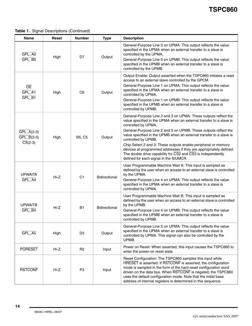
PORESET Hi-Z R2 InputPower on Reset: When asserted, this input causes the TSPC860 to enter the power-on reset state.
RSTCONF Hi-Z P3 Input
Reset Configuration: The TSPC860 samples this input while HRESET is asserted. If RSTCONF is asserted, the configuration mode is sampled in the form of the hard reset configuration word driven on the data bus. When RSTCONF is negated, the TSPC860 uses the default configuration mode. Note that the initial base address of internal registers is determined in this sequence.
Table 1. Signal Descriptions (Continued)
Name Reset Number Type Description
140843C–HIREL–06/07
e2v semiconductors SAS 2007

TSPC860
HRESET Low N4 Open-drainHard Reset: Asserting this open drain signal puts the TSPC860 in hard reset state.
SRESET Low P2 Open-drainSoft Reset: Asserting this open drain line puts the TSPC860 in soft reset state.
XTALAnalog Driving
P1Analog Output
This output is one of the connections to an external crystal for the internal oscillator circuitry.
EXTAL Hi-Z N1Analog Input (3.3V only)
This line is one of the connections to an external crystal for the internal oscillator circuitry.
XFCAnalog Driving
T2 Analog InputExternal Filter Capacitance: This input is the connection pin for an external capacitor filter for the PLL circuitry.
CLKOUT
High until SPLL locked,
then oscillating
W3 Output Clock Out: This output is the clock system frequency.
EXTCLK Hi-Z N2Input (3.3V
only)External Clock : This input is the external input clock from an external source.
TEXP High N3 Output Timer Expired: This output reflects the status of PLPRCR[TEXPS].
ALE_A Low K2 OutputAddress Latch Enable A: This output is asserted when TSPC860 initiates an access to a region under the control of the PCMCIA interface to socket A.
CE1_A High B3 OutputCard Enable 1 Slot A: This output enables even byte transfers when accesses to PCMCIA Slot A are handled under the control of the PCMCIA interface.
CE2_A High A3 OutputCard Enable 2 Slot A: This output enables odd byte transfers when accesses to PCMCIA Slot A are handled under the control of the PCMCIA interface.
WAIT_A Hi-Z R3 InputWait Slot A: This input, if asserted low, causes a delay in the completion of a transaction on the PCMCIA controlled Slot A.
WAIT_B Hi-Z R4 InputWait Slot B: This input, if asserted low, causes a delay in the completion of a transaction on the PCMCIA controlled Slot B.
IP_A(0-1) Hi-Z T5, T4 InputInput Port A 0-1: The TSPC860 monitors these inputs that are reflected in the PIPR and PSCR of the PCMCIA interface.
IP_A2IOIS16_A
Hi-Z U3 Input
Input Port A 2: The TSPC860 monitors these inputs; its value and changes are reported in the PIPR and PSCR of the PCMCIA interface. I/O Device A is 16-Bits Ports Size: The TSPC860 monitors this input when a transaction under the control of the PCMCIA interface is initiated to an I/O region in socket A of the PCMCIA space.
IP_A(3-7) Hi-ZW2, U4,
U5, T6, T3Input
Input Port A 3-7: The TSPC860 monitors these inputs; their values and changes are reported in the PIPR and PSCR of the PCMCIA interface.
Table 1. Signal Descriptions (Continued)
Name Reset Number Type Description
150843C–HIREL–06/07
e2v semiconductors SAS 2007
TSPC860
ALE_B
DSCK/AT1
See Section “Signal
States During Hardware Reset” on page 29
J1BidirectionalThree-state
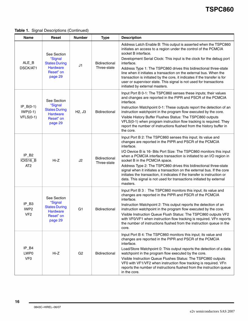
Address Latch Enable B: This output is asserted when the TSPC860 initiates an access to a region under the control of the PCMCIA socket B interface. Development Serial Clock: This input is the clock for the debug port interface.
Address Type 1: The TSPC860 drives this bidirectional three-state line when it initiates a transaction on the external bus. When the transaction is initiated by the core, it indicates if the transfer is for user or supervisor state. This signal is not used for transactions initiated by external masters.
IP_B(0-1)
IWP(0-1)
VFLS(0-1)
See Section “Signal
States During Hardware Reset” on page 29
H2, J3 Bidirectional
Input Port B 0-1: The TSPC860 senses these inputs; their values and changes are reported in the PIPR and PSCR of the PCMCIA interface.
Instruction Watchpoint 0-1: These outputs report the detection of an instruction watchpoint in the program flow executed by the core.
Visible History Buffer Flushes Status: The TSPC860 outputs VFLS(0-1) when program instruction flow tracking is required. They report the number of instructions flushed from the history buffer in the core.
IP_B2
IOIS16_B
AT2
Hi-Z J2BidirectionalThree-state
Input Port B 2: The TSPC860 senses this input; its value and changes are reported in the PIPR and PSCR of the PCMCIA interface. I/O Device B is 16- Bits Port Size: The TSPC860 monitors this input when a PCMCIA interface transaction is initiated to an I/O region in socket B in the PCMCIA space.
Address Type 2: The TSPC860 drives this bidirectional three-state signal when it initiates a transaction on the external bus. If the core initiates the transaction, it indicates if the transfer is instruction or data. This signal is not used for transactions initiated by external masters.
IP_B3
IWP2
VF2
See Section “Signal
States During Hardware Reset” on page 29
G1 Bidirectional
Input Port B 3 : The TSPC860 monitors this input; its value and changes are reported in the PIPR and PSCR of the PCMCIA interface.
Instruction Watchpoint 2: This output reports the detection of an instruction watchpoint in the program flow executed by the core.
Visible Instruction Queue Flush Status: The TSPC860 outputs VF2 with VF0/VF1 when instruction flow tracking is required. VFn reports the number of instructions flushed from the instruction queue in the core.
IP_B4
LWP0VF0
Hi-Z G2 Bidirectional
Input Port B 4: The TSPC860 monitors this input; its value and changes are reported in the PIPR and PSCR of the PCMCIA interface. Load/Store Watchpoint 0: This output reports the detection of a data watchpoint in the program flow executed by the core. Visible Instruction Queue Flushes Status: The TSPC860 outputs VF0 with VF1/VF2 when instruction flow tracking is required. VFn reports the number of instructions flushed from the instruction queue in the core.
Table 1. Signal Descriptions (Continued)
Name Reset Number Type Description
160843C–HIREL–06/07
e2v semiconductors SAS 2007

TSPC860
IP_B5
LWP1
VF1
Hi-Z J4 Bidirectional
Input Port B 5: The TSPC860 monitors this input; its value and changes are reported in the PIPR and PSCR of the PCMCIA interface. Load/Store Watchpoint 1: This output reports the detection of a data watchpoint in the program flow executed by the core.
Visible Instruction Queue Flushes Status: The TSPC860 outputs VF1 with VF0 and VF2 when instruction flow tracking is required. VFn reports the number of instructions flushed from the instruction queue in the core.
IP_B6
DSDIAT0
Hi-Z K3BidirectionalThree-state
Input Port B 6: The TSPC860 senses this input and its value and changes are reported in the PIPR and PSCR of the PCMCIA interface.Development Serial Data Input: Data input for the debug port interface.Address Type 0: The TSPC860 drives this bidirectional three-state line when it initiates a transaction on the external bus. If high (1), the transaction is the CPM. If low (0), the transaction initiator is the CPU. This signal is not used for transactions initiated by external masters.
IP_B7
PTR
AT3
Hi-Z H1BidirectionalThree-state
Input Port B 7: The TSPC860 monitors this input; its value and changes are reported in the PIPR and PSCR of the PCMCIA interface.
Program Trace: To allow program flow tracking, the TSPC860 asserts this output to indicate an instruction fetch is taking place.
Address Type 3: The TSPC860 drives the bidirectional three-state signal when it starts a transaction on the external bus. When the core initiates a transfer, AT3 indicates whether it is a reservation for a data transfer or a program trace indication for an instruction fetch. This signal is not used for transactions initiated by external masters.
OP(0-1) Low L4, L2 OutputOutput Port 0-1: The TSPC860 generates these outputs as a result of a write to the PGCRA register in the PCMCIA interface.
OP2
MODCK1STS
Hi-Z L1 Bidirectional
Output Port 2: This output is generated by the TSPC860 as a result of a write to the PGCRB register in the PCMCIA interface. Mode Clock 1: Input sampled when PORESET is negated to configure PLL/clock mode. Special Transfer Start: The TSPC860 drives this output to indicate the start of an external bus transfer or of an internal transaction in show-cycle mode.
OP3
MODCK2
DSDO
Hi-Z M4 Bidirectional
Output Port 3: This output is generated by the TSPC860 as a result of a write to the PGCRB register in the PCMCIA interface. Mode Clock 2: This input is sampled at the PORESET negation to configure the PLL/clock mode of operation. Development Serial Data Output: Output data from the debug port interface.
Table 1. Signal Descriptions (Continued)
Name Reset Number Type Description
170843C–HIREL–06/07
e2v semiconductors SAS 2007
TSPC860
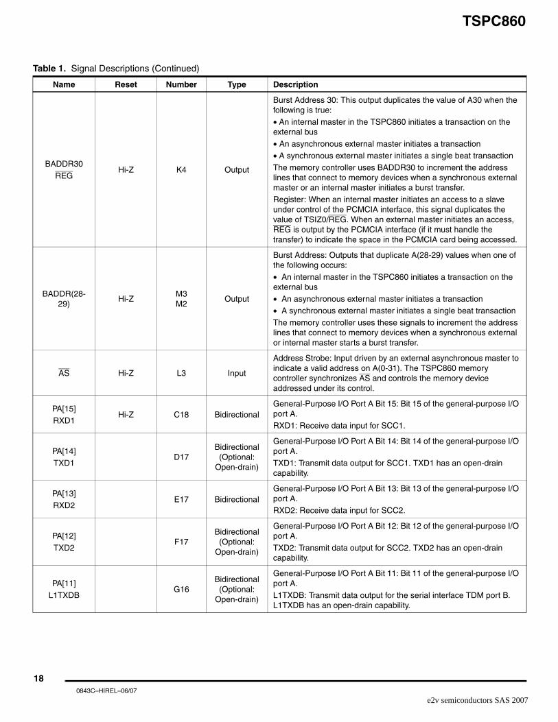
BADDR30
REGHi-Z K4 Output
Burst Address 30: This output duplicates the value of A30 when the following is true:
• An internal master in the TSPC860 initiates a transaction on the external bus
• An asynchronous external master initiates a transaction
• A synchronous external master initiates a single beat transaction
The memory controller uses BADDR30 to increment the address lines that connect to memory devices when a synchronous external master or an internal master initiates a burst transfer.
Register: When an internal master initiates an access to a slave under control of the PCMCIA interface, this signal duplicates the value of TSIZ0/REG. When an external master initiates an access, REG is output by the PCMCIA interface (if it must handle the transfer) to indicate the space in the PCMCIA card being accessed.
BADDR(28-29)
Hi-ZM3M2
Output
Burst Address: Outputs that duplicate A(28-29) values when one of the following occurs:
• An internal master in the TSPC860 initiates a transaction on the external bus
• An asynchronous external master initiates a transaction• A synchronous external master initiates a single beat transaction
The memory controller uses these signals to increment the address lines that connect to memory devices when a synchronous external or internal master starts a burst transfer.
AS Hi-Z L3 Input
Address Strobe: Input driven by an external asynchronous master to indicate a valid address on A(0-31). The TSPC860 memory controller synchronizes AS and controls the memory device addressed under its control.
PA[15]
RXD1Hi-Z C18 Bidirectional
General-Purpose I/O Port A Bit 15: Bit 15 of the general-purpose I/O port A. RXD1: Receive data input for SCC1.
PA[14]
TXD1D17
Bidirectional(Optional:
Open-drain)
General-Purpose I/O Port A Bit 14: Bit 14 of the general-purpose I/O port A.
TXD1: Transmit data output for SCC1. TXD1 has an open-drain capability.
PA[13]
RXD2E17 Bidirectional
General-Purpose I/O Port A Bit 13: Bit 13 of the general-purpose I/O port A. RXD2: Receive data input for SCC2.
PA[12]
TXD2F17
Bidirectional(Optional:
Open-drain)
General-Purpose I/O Port A Bit 12: Bit 12 of the general-purpose I/O port A.
TXD2: Transmit data output for SCC2. TXD2 has an open-drain capability.
PA[11]
L1TXDBG16
Bidirectional(Optional:
Open-drain)
General-Purpose I/O Port A Bit 11: Bit 11 of the general-purpose I/O port A.
L1TXDB: Transmit data output for the serial interface TDM port B. L1TXDB has an open-drain capability.
Table 1. Signal Descriptions (Continued)
Name Reset Number Type Description
180843C–HIREL–06/07
e2v semiconductors SAS 2007
TSPC860
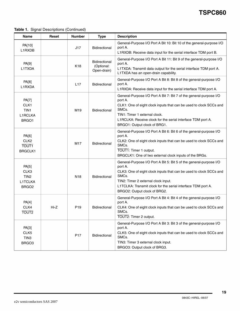
PA[10]L1RXDB
J17 BidirectionalGeneral-Purpose I/O Port A Bit 10: Bit 10 of the general-purpose I/O port A.
L1RXDB: Receive data input for the serial interface TDM port B.
PA[9]
L1TXDAK18
Bidirectional(Optional:
Open-drain)
General-Purpose I/O Port A Bit 11: Bit 9 of the general-purpose I/O port A.
L1TXDA: Transmit data output for the serial interface TDM port A. L1TXDA has an open-drain capability.
PA[8]
L1RXDAL17 Bidirectional
General-Purpose I/O Port A Bit 8: Bit 8 of the general-purpose I/O port A. L1RXDA: Receive data input for the serial interface TDM port A.
PA[7]
CLK1TIN1
L1RCLKA
BRGO1
M19 Bidirectional
General-Purpose I/O Port A Bit 7: Bit 7 of the general-purpose I/O port A.
CLK1: One of eight clock inputs that can be used to clock SCCs and SMCs.
TIN1: Timer 1 external clock. L1RCLKA: Receive clock for the serial interface TDM port A.
BRGO1: Output clock of BRG1.
PA[6]CLK2
TOUT1
BRGCLK1
M17 Bidirectional
General-Purpose I/O Port A Bit 6: Bit 6 of the general-purpose I/O port A. CLK2: One of eight clock inputs that can be used to clock SCCs and SMCs. TOUT1: Timer 1 output.
BRGCLK1: One of two external clock inputs of the BRGs.
PA[5]CLK3
TIN2
L1TCLKABRGO2
N18 Bidirectional
General-Purpose I/O Port A Bit 5: Bit 5 of the general-purpose I/O port A. CLK3: One of eight clock inputs that can be used to clock SCCs and SMCs. TIN2: Timer 2 external clock input.
L1TCLKA: Transmit clock for the serial interface TDM port A.
BRGO2: Output clock of BRG2.
PA[4]
CLK4
TOUT2
Hi-Z P19 Bidirectional
General-Purpose I/O Port A Bit 4: Bit 4 of the general-purpose I/O port A.
CLK4: One of eight clock inputs that can be used to clock SCCs and SMCs.
TOUT2: Timer 2 output.
PA[3]CLK5
TIN3
BRGO3
P17 Bidirectional
General-Purpose I/O Port A Bit 3: Bit 3 of the general-purpose I/O port A. CLK5: One of eight clock inputs that can be used to clock SCCs and SMCs. TIN3: Timer 3 external clock input.
BRGO3: Output clock of BRG3.
Table 1. Signal Descriptions (Continued)
Name Reset Number Type Description
190843C–HIREL–06/07
e2v semiconductors SAS 2007
TSPC860
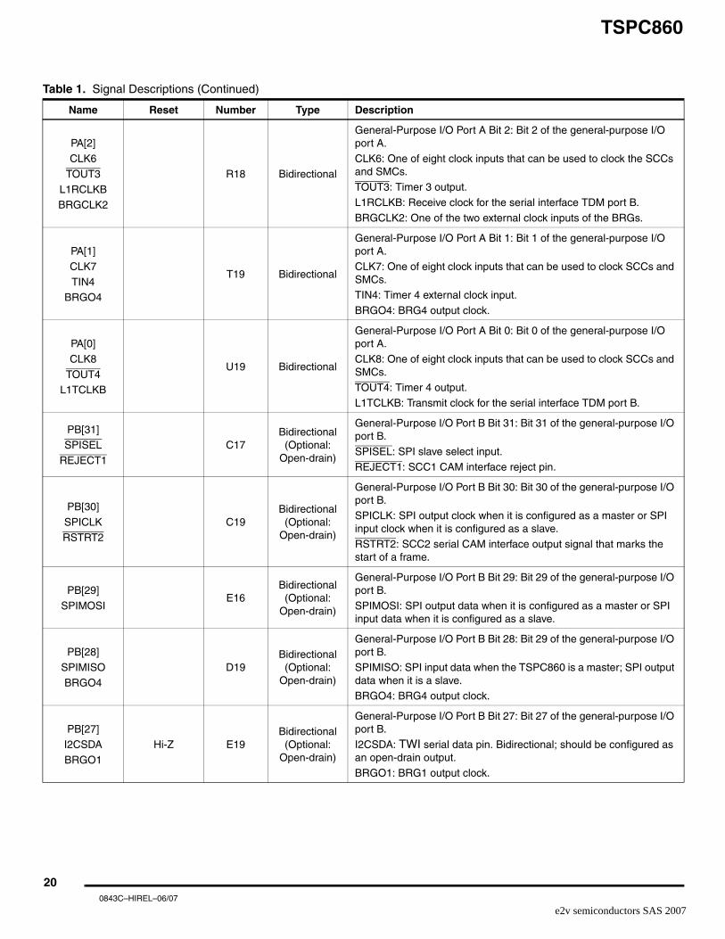
PA[2]
CLK6
TOUT3
L1RCLKBBRGCLK2
R18 Bidirectional
General-Purpose I/O Port A Bit 2: Bit 2 of the general-purpose I/O port A.
CLK6: One of eight clock inputs that can be used to clock the SCCs and SMCs.
TOUT3: Timer 3 output.
L1RCLKB: Receive clock for the serial interface TDM port B.
BRGCLK2: One of the two external clock inputs of the BRGs.
PA[1]
CLK7
TIN4BRGO4
T19 Bidirectional
General-Purpose I/O Port A Bit 1: Bit 1 of the general-purpose I/O port A.
CLK7: One of eight clock inputs that can be used to clock SCCs and SMCs.
TIN4: Timer 4 external clock input.
BRGO4: BRG4 output clock.
PA[0]
CLK8
TOUT4L1TCLKB
U19 Bidirectional
General-Purpose I/O Port A Bit 0: Bit 0 of the general-purpose I/O port A.
CLK8: One of eight clock inputs that can be used to clock SCCs and SMCs.
TOUT4: Timer 4 output.
L1TCLKB: Transmit clock for the serial interface TDM port B.
PB[31]SPISEL
REJECT1
C17Bidirectional(Optional:
Open-drain)
General-Purpose I/O Port B Bit 31: Bit 31 of the general-purpose I/O port B.
SPISEL: SPI slave select input.
REJECT1: SCC1 CAM interface reject pin.
PB[30]
SPICLKRSTRT2
C19Bidirectional(Optional:
Open-drain)
General-Purpose I/O Port B Bit 30: Bit 30 of the general-purpose I/O port B.
SPICLK: SPI output clock when it is configured as a master or SPI input clock when it is configured as a slave.
RSTRT2: SCC2 serial CAM interface output signal that marks the start of a frame.
PB[29]
SPIMOSI E16
Bidirectional(Optional:
Open-drain)
General-Purpose I/O Port B Bit 29: Bit 29 of the general-purpose I/O port B.
SPIMOSI: SPI output data when it is configured as a master or SPI input data when it is configured as a slave.
PB[28]SPIMISO
BRGO4
D19Bidirectional(Optional:
Open-drain)
General-Purpose I/O Port B Bit 28: Bit 29 of the general-purpose I/O port B. SPIMISO: SPI input data when the TSPC860 is a master; SPI output data when it is a slave. BRGO4: BRG4 output clock.
PB[27]
I2CSDA
BRGO1
Hi-Z E19Bidirectional(Optional:
Open-drain)
General-Purpose I/O Port B Bit 27: Bit 27 of the general-purpose I/O port B.
I2CSDA: TWI serial data pin. Bidirectional; should be configured as an open-drain output.
BRGO1: BRG1 output clock.
Table 1. Signal Descriptions (Continued)
Name Reset Number Type Description
200843C–HIREL–06/07
e2v semiconductors SAS 2007

TSPC860
PB[26]
I2CSCL
BRGO2
F19Bidirectional(Optional:
Open-drain)
General-Purpose I/O Port B Bit 26: Bit 26 of the general-purpose I/O port B.
I2CSCL: TWI serial clock pin. Bidirectional; should be configured as an open-drain output.
BRGO2: BRG2 output clock.
PB[25]
SMTXD1J16
Bidirectional(Optional:
Open-drain)
General-Purpose I/O Port B Bit 25: Bit 25 of the general-purpose I/O port B.
SMTXD1: SMC1 transmit data output.
PB[24]SMRXD1
J18Bidirectional(Optional:
Open-drain)
General-Purpose I/O Port B Bit 24: Bit 24 of the general-purpose I/O port B.
SMRXD1: SMC1 receive data input.
PB[23]
SMSYN1
SDACK1
K17Bidirectional(Optional:
Open-drain)
General-Purpose I/O Port B Bit 23: Bit 23 of the general-purpose I/O port B. SMSYN1: SMC1 external sync input.
SDACK1: SDMA acknowledge 1 output that is used as a peripheral interface signal for IDMA emulation, or as a CAM interface signal for Ethernet.
PB[22]
SMSYN2SDACK2
L19Bidirectional(Optional:
Open-drain)
General-Purpose I/O Port B Bit 22: Bit 22 of the general-purpose I/O port B.
SMSYN2: SMC2 external sync input.
SDACK2: SDMA acknowledge 2 output that is used as a peripheral interface signal for IDMA emulation, or as a CAM interface signal for Ethernet.
PB[21]
SMTXD2
L1CLKOB
K16Bidirectional(Optional:
Open-drain)
General-Purpose I/O Port B Bit 21: Bit 21 of the general-purpose I/O port B.
SMTXD2: SMC2 transmit data output. L1CLKOB: Clock output from the serial interface TDM port B.
PB[20]
SMRXD2
L1CLKOA
L16Bidirectional(Optional:
Open-drain)
General-Purpose I/O Port B Bit 20: Bit 20 of the general-purpose I/O port B.
SMRXD2: SMC2 receive data input. L1CLKOA: Clock output from the serial interface TDM port A.
PB[19]
RTS1L1ST1
N19Bidirectional(Optional:
Open-drain)
General-Purpose I/O Port B Bit 19: Bit 19 of the general-purpose I/O port B.
RTS1: Request to send modem line for SCC1. L1ST1: One of four output strobes that can be generated by the serial interface.
PB[18]
RTS2
L1ST2
N17Bidirectional(Optional:
Open-drain)
General-Purpose I/O Port B Bit 18: Bit 18 of the general-purpose I/O port B.
RTS2: Request to send modem line for SCC2.
L1ST2: One of four output strobes that can be generated by the serial interface.
PB[17]
L1RQBL1ST3
Hi-Z P18Bidirectional(Optional:
Open-drain)
General-Purpose I/O Port B Bit 17: Bit 17 of the general-purpose I/O port B.
L1RQB: D-channel request signal for the serial interface TDM port B. L1ST3: One of four output strobes that can be generated by the serial interface.
Table 1. Signal Descriptions (Continued)
Name Reset Number Type Description
210843C–HIREL–06/07
e2v semiconductors SAS 2007

TSPC860
PB[16]
L1RQA
L1ST4
N16Bidirectional(Optional:
Open-drain)
General-Purpose I/O Port B Bit 16: Bit 16 of the general-purpose I/O port B.
L1RQA: D-channel request signal for the serial interface TDM port A.
L1ST4: One of four output strobes that can be generated by the serial interface.
PB[15]
BRGO3R17 Bidirectional
General-Purpose I/O Port B Bit 15: Bit 15 of the general-purpose I/O port B.
BRGO3: BRG3 output clock.
PB[14]
RSTRT1U18 Bidirectional
General-Purpose I/O Port B Bit 14: Bit 14 of the general-purpose I/O port B.
RSTRT1: SCC1 serial CAM interface outputs that marks the start of a frame.
PC[15]
DREQ0RTS1
L1ST1
D16 Bidirectional
General-Purpose I/O Port C Bit 15: Bit 15 of the general-purpose I/O port C.
DREQ0: IDMA channel 0 request input. RTS1: Request to send modem line for SCC1.
L1ST1: One of four output strobes that can be generated by the serial interface.
PC[14]
DREQ1RTS2
L1ST2
D18 Bidirectional
General-Purpose I/O Port C Bit 14: Bit 14 of the general-purpose I/O port C.
DREQ1: IDMA channel 1 request input. RTS2: Request to send modem line for SCC2.
L1ST2: One of four output strobes that can be generated by the serial interface.
PC[13]
L1RQBL1ST3
E18 Bidirectional
General-Purpose I/O Port C Bit 13: Bit 13 of the general-purpose I/O port C.
L1RQB: D-channel request signal for the serial interface TDM port B. L1ST3: One of four output strobes that can be generated by the serial interface.
PC[12]
L1RQA
L1ST4
F18 Bidirectional
General-Purpose I/O Port C Bit 12: Bit 12 of the general-purpose I/O port C.
L1RQA: D-channel request signal for the serial interface TDM port A.
L1ST4: One of four output strobes that can be generated by the serial interface.
PC[11]
CTS1J19 Bidirectional
General-Purpose I/O Port C Bit 11: Bit 11 of the general-purpose I/O port C. CTS1: Clear to send modem line for SCC1.
PC[10]
CD1
TGATE1
Hi-Z K19 Bidirectional
General-Purpose I/O Port C Bit 10: Bit 10 of the general-purpose I/O port C.
CD1: Carrier detect modem line for SCC1. TGATE1: Timer 1/timer 2 gate signal.
PC[9]CTS2
L18 BidirectionalGeneral-Purpose I/O Port C Bit 9: Bit 9 of the general-purpose I/O port C.
CTS2: Clear to send modem line for SCC2.
Table 1. Signal Descriptions (Continued)
Name Reset Number Type Description
220843C–HIREL–06/07
e2v semiconductors SAS 2007

TSPC860
PC[8]CD2
TGATE2
M18 Bidirectional
General-Purpose I/O Port C Bit 8: Bit 8 of the general-purpose I/O port C.
CD2: Carrier detect modem line for SCC2.
TGATE2: Timer 3/timer 4 gate signal.
PC[7]
CTS3
L1TSYNCBSDACK2
M16 Bidirectional
General-Purpose I/O Port C Bit 7: Bit 7 of the general-purpose I/O port C. CTS3: Clear to send modem line for SCC3.
L1TSYNCB: Transmit sync input for the serial interface TDM port B.
SDACK2: SDMA acknowledge 2 output that is used as a peripheral interface signal for IDMA emulation or as a CAM interface signal for Ethernet.
PC[6]
CD3
L1RSYNCB
R19 Bidirectional
General-Purpose I/O Port C Bit 6: Bit 6 of the general-purpose I/O port C.
CD3: Carrier detect modem line for SCC3.L1RSYNCB: Receive sync input for the serial interface TDM port B.
PC[5]CTS4
L1TSYNCA
SDACK1
T18 Bidirectional
General-Purpose I/O Port C Bit 5: Bit 5 of the general-purpose I/O port C.
CTS4: Clear to send modem line for SCC4.L1TSYNCA: Transmit sync input for the serial interface TDM port A.
SDACK1: SDMA acknowledge 1output that is used as a peripheral interface signal for IDMA emulation or as a CAM interface signal for Ethernet.
PC[4]CD4
L1RSYNCA
T17 Bidirectional
General-Purpose I/O Port C Bit 4: Bit 4 of the general-purpose I/O port C.
CD4: Carrier detect modem line for SCC4.
L1RSYNCA: Receive sync input for the serial interface TDM port A.
PD[15]L1TSYNCA
U17 BidirectionalGeneral-Purpose I/O Port D Bit 15: Bit 15 of the general-purpose I/O port D.
L1TSYNCA: Input transmit data sync signal to the TDM channel A.
PD[14]
L1RSYNCAV19 Bidirectional
General-Purpose I/O Port D Bit 14: Bit 14 of the general-purpose I/O port D. L1RSYNCA: Input receive data sync signal to the TDM channel A.
PD[13]
L1TSYNCBV18 Bidirectional
General-Purpose I/O Port D Bit 13: Bit 13 of the general-purpose I/O port D.
L1TSYNCB: Input transmit data sync signal to the TDM channel B.
PD[12]L1RSYNCB
Hi-Z R16 BidirectionalGeneral-Purpose I/O Port D Bit 12: Bit 12 of the general-purpose I/O port D.
L1RSYNCB: Input receive data sync signal to the TDM channel B.
PD[11]
RXD3T16 Bidirectional
General-Purpose I/O Port D Bit 11: Bit 11 of the general-purpose I/O port D. RXD3: Receive data for serial channel 3.
PD[10]TXD3
W18 BidirectionalGeneral-Purpose I/O Port D Bit 10: Bit 10 of the general-purpose I/O port D.
TXD3: Transmit data for serial channel 3.
Table 1. Signal Descriptions (Continued)
Name Reset Number Type Description
230843C–HIREL–06/07
e2v semiconductors SAS 2007

TSPC860
PD[9]RXD4
V17 BidirectionalGeneral-Purpose I/O Port D Bit 9 : Bit 9 of the general-purpose I/O port D.
RXD4: Receive data for serial channel 4.
PD[8]
TXD4W17 Bidirectional
General-Purpose I/O Port D Bit 8: Bit 8 of the general-purpose I/O port D.
TXD4: Transmit data for serial channel 4.
PD[7]
RTS3T15 Bidirectional
General-Purpose I/O Port D Bit 7: Bit 7 of the general-purpose I/O port D.
RTS3: Active low request to send output indicates that SCC3 is ready to transmit data.
PD[6]
RTS4V16 Bidirectional
General-Purpose I/O Port D Bit 6: Bit 6 of the general-purpose I/O port D.
RTS4: Active low request to send output indicates that SCC4 is ready to transmit data.
PD[5]REJECT2
U15 Bidirectional
General-Purpose I/O Port D Bit 5: Bit 5 of the general-purpose I/O port D. REJECT2: This input to SCC2 allows a CAM to reject the current Ethernet frame after it determines the frame address did not match.
PD[4]
REJECT3U16 Bidirectional
General-Purpose I/O Port D Bit 4: Bit 4 of the general-purpose I/O port D.
REJECT3: This input to SCC3 allows a CAM to reject the current Ethernet frame after it determines the frame address did not match.
PD[3]
REJECT4W16 Bidirectional
General-Purpose I/O Port D Bit 3: Bit 3 of the general-purpose I/O port D.
REJECT4: This input to SCC4 allows a CAM to reject the current Ethernet frame after it determines the frame address did not match.
TCKDSCK
Hi-Z (Pulled up on rev 0 to
rev A.3) H16 Input
Provides clock to scan chain logic or for the development port logic. Should be tied to Vcc if JTAG or development port are not used.
TMS Pulled up G18 InputControls the scan chain test mode operations. Should be tied to power through a pull-up resistor if unused.
TDIDSDI
Pulled up (Hi-Z on rev 0 to
rev A.3)H17 Input
Input serial data for either the scan chain logic or the development port and determines the operating mode of the development port at reset.
TDODSDO
Low G17 OutputOutput serial data for either the scan chain logic or for the development port.
Table 1. Signal Descriptions (Continued)
Name Reset Number Type Description
240843C–HIREL–06/07
e2v semiconductors SAS 2007
TSPC860
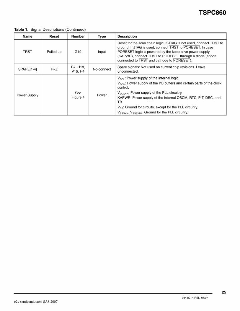
TRST Pulled up G19 Input
Reset for the scan chain logic. If JTAG is not used, connect TRST to ground. If JTAG is used, connect TRST to PORESET. In case PORESET logic is powered by the keep-alive power supply (KAPWR), connect TRST to PORESET through a diode (anode connected to TRST and cathode to PORESET).
SPARE[1-4] Hi-ZB7, H18, V15, H4
No-connectSpare signals: Not used on current chip revisions. Leave unconnected.
Power SupplySee
Figure 4Power
VDDL: Power supply of the internal logic.VDDH: Power supply of the I/O buffers and certain parts of the clock control. VDDSYN: Power supply of the PLL circuitry.
KAPWR: Power supply of the internal OSCM, RTC, PIT, DEC, and TB.
VSS: Ground for circuits, except for the PLL circuitry.
VSSSYN, VSSSYN1: Ground for the PLL circuitry.
Table 1. Signal Descriptions (Continued)
Name Reset Number Type Description
250843C–HIREL–06/07
e2v semiconductors SAS 2007

TSPC860
5.1 Active Pull-up BuffersActive pull-up buffers are a special variety of bidirectional three-state buffer with the following properties:
• When enabled as an output and driving low, they behave as normal output drivers (that is, the pin is constantly driven low).
• When enabled as an output and driving high, drive high until an internal detection circuit determines that the output has reached the logic high threshold and then stop driving (that is, the pin switches to high-impedance).
• When disabled as an output or functioning as an input, it should not be driven.
Due to the behavior of the buffer when being driven high, a pull-up resistor is required externally to func-tion as a ‘bus keep’ for these shared signals in periods when no drivers are active and to keep the bufferfrom oscillating when the buffer is driving high, because if the voltage ever dips below the logic highthreshold while the buffer is enabled as an output, the buffer will reactivate. Further, external logic mustnot attempt to drive these signals low while active pull-up buffers are enabled as outputs, because thebuffers will reactivate and drive high, resulting in a buffer fight and possible damage to the TSPC860, tothe system, or to both.
Figure 5-1 compares three-state buffers and active pull-up buffers graphically in general terms. It makesno implication as to which edges trigger which events for any particular signal.
Figure 5-1. Three-State Buffers and Active Pull-Up Buffers
Note: Events 1 and 4 can be in quick succession.
1 2
3
1 2
3 5
4
1 Drive high on one edge2 Switch to Hi-Z on later edge3 Pull-up resistor maintains logic high state
1 Drive high on one edge2 Switch to Hi-Z when threshold voltage
(Voh + margin) is reached3 Pull-up resistor maintains logic high state4 Disable buffer as output5 Pull-up resistor maintains logic high state;
other driver can drive signal
Three-statebuffer
Activepull-upbuffer
260843C–HIREL–06/07
e2v semiconductors SAS 2007

TSPC860
Table 5-1 summarizes when active pull-up drivers are enabled as outputs.
The purpose of active pull-up buffers is to allow access to zero wait-state logic that drives a shared sig-nal on the clock cycle immediately following a cycle in which the signal is driven by the TSPC860. Inother words, it eliminates the need for a bus turn-around cycle.
5.2 Internal Pull-up and Pull-down ResistorsThe TMS and TRST pins have internal pull-up resistors. TSPC860 devices from Rev 0 to Rev A.3(masks xE64C and xF84C) have an internal pull-up resistor on TCK/DSCK but no internal pull-up resis-tor on TDI/DSDI. This was corrected on Rev B and later; on these chips, the internal pull-up resistor wasremoved from TCK/DSCK and an internal pull-up resistor was added to TDI/DSDI.
If RSTCONF is pulled down, during hardware reset (initiated by HRESET or PORESET), the data busD[0-31] is pulled down with internal pull-down resistors. These internal pull-down resistors are to providea logic-zero default for these pins when programming the hard reset configuration word. These internalpull-down resistors are disconnected after HRESET is negated.
No other pins have internal pull-ups or pull-downs.
Resistance values for internal pull-up and pull-down resistors are not specified because their values mayvary due to process variations and shrinks in die size, and they are not tested. Typical values are on theorder of 5 KΩ but can vary by approximately a factor of 2.
5.3 Recommended Basic Pin Connections
5.3.1 Reset ConfigurationSome external pin configuration is determined at reset by the hard reset configuration word. Thus, somedecisions as to system configuration (for example, location of BDM pins) should be made beforerequired application of pull-up and pull-down resistors can be determined.
RSTCONF should be grounded if the hard reset configuration word is used to configure the TSPC860 orshould be connected to VCC if the default configuration is used.
Pull-up resistors may not be used on D[0-31] to set the hard reset configuration word, as the values ofthe internal pull-down resistors are not specified or guaranteed. To change a data bus signal from itsdefault logic low state during reset, actively drive that signal high.
Table 5-1. Active Pull-Up Resistors Enabled as Outputs
Signal Description
TS, BB When the TSPC860 is the external bus master throughout the entire bus cycle.
BI When the TSPC860’s memory controller responds to the access on the external bus, throughout the entire bus cycle.
TA
When the TSPC860’s memory controller responds to the access on the external bus, then:• For chip-selects controlled by the GPCM set for external TA, the TSPC860’s TA buffer is not enabled as an output.
• For chip-selects controlled by the GPCM set to terminate in n wait-states, TA is enabled as an output on cycle (n-1) and driven high, then is driven low on cycle n, terminating the bus transaction. External logic can drive TA at any point before this, thus terminating the cycle early. [For example, assume the GPCM is programmed to drive TA after 15 cycles. If external logic drives TA before 14 clocks have elapsed then the TA will be accepted by the TSPC860 as a cycle termination.]
• For chip-selects controlled by the UPM, the TA buffer is enabled as an output throughout the entire bus cycle.
270843C–HIREL–06/07
e2v semiconductors SAS 2007

TSPC860
MODCK[1-2] must be used to determine the default clocking mode for the TSPC860. After hardwarereset, the MODCK[1-2] pins change function and become outputs. Thus, if these alternate functions arealso desired, then the MODCK[1-2] configuration should be set with three-state drivers that turn off afterHRESET is negated; however, if MODCK[1-2] pins’ alternate output functions are not used in the sys-tem, they can be configured with pull-up and pull-down resistors.
Signals with open-drain buffers and active pull-up buffers (HRESET, SRESET, TEA, TS, TA, BI, and BB)must have external pull-up resistors. These signals include the following:
Some other input signals do not absolutely require a pull-up resistor, as they may be actively driven byexternal logic. However, if they are not used externally, or if the external logic connected to them is notalways actively driving, they may need external pull-up resistors to hold them negated. These signalsinclude the following:
• PORESET
• AS
• CR/IRQ3
• KR/RETRY/IRQ4/SPKROUT (if configured as KR/RETRY or IRQ4)
• Any IRQx (if configured as IRQx)
• BR (if the TSPC860’s internal bus arbiter is used)
• BG (if an external bus arbiter is used)
5.3.2 JTAG and Debug PortsTCK/DSCK or ALE_B/DSCK/AT1 (depending on the configuration of the DSCK function) should be con-nected to ground through a pull-down resistor to disable Debug Mode as a default. When required, adebug mode controller tool externally drives this signal high actively to put the TSPC860 into debugmode.
Two pins need special attention, depending on the version of TSPC860 used.
• For TSPC860 rev B and later, TDI/DSDI should be pulled up to VCC to keep it from oscillating when unused.
• For TSPC860 rev A.3 and earlier, TCK/DSCK should be connected to ground if it is configured for its DSCK function, as stated above. However, for these versions of the TSPC860, the pull-down resistor must be strong (for example, 1 kΩ to overcome the internal pull-up resistor.
To allow application of any version of processor, perform both of the above actions.
5.3.3 Unused InputsIn general, pull-up resistors should be used on any unused inputs to keep them from oscillating. Forexample, if PCMCIA is not used, the PCMCIA input pins (WAIT_A, WAIT_B, IP_A[0-8], IP_B[0-8])should have external pull-up resistors. However, unused pins of port A, B, C, or D can be configured asoutputs, and, if they are configured as outputs they do not require external terminations.
5.3.4 Unused OutputsUnused outputs can be left unterminated.
280843C–HIREL–06/07
e2v semiconductors SAS 2007

TSPC860
5.4 Signal States During Hardware ResetDuring hardware reset (HRESET or PORESET), the signals of the TSPC860 behave as follows:
• The bus signals are high-impedance
• The port I/O signals are configured as inputs, and are therefore high-impedance
• The memory controller signals are driven to their inactive state
However, some signal functions are determined by the reset configuration. When HRESET is asserted,these signals immediately begin functioning as determined by the reset configuration and are eitherhigh-impedance or are drive to their inactive state accordingly. The behavior of these signals is shown inTable 8-6.
Table 5-2. Signal States during Hardware Reset
Signal Behavior
BDIP/GPL_B5BDIP: high impedanceGPL_B5: high
RSV/IRQ2RSV: highIRQ2: high impedance
KR/RETRY/IRQ4/SPKROUTKR/RETRY/IRQ4: high impedanceSPKROUT: low
FRZ/IRQ6FRZ: lowIRQ6: high impedance
ALE_B/DSCK/AT1ALE_B: lowDSCK/AT1: high impedance
IP_B[0-1]/IWP[0-1]/VFLS[0-1]IP_B[0-1]: high impedanceIWP[0-1]: high
VFLS[0-1]: low
IP_B3/IWP2/VF2
IP_B3: high impedance
IWP2: high
VF2: low
IP_B4/LWP0/VF0
IP_B4: high impedance
LWP0: highVF0: low
IP_B5/LWP1/VF1IP_B5: high impedanceLWP1: high;
VF1: low
290843C–HIREL–06/07
e2v semiconductors SAS 2007

TSPC860
6. Detailed SpecificationsThis specifications describes the specific requirements for the microcontroller TSPC860, in compliancewith MIL-STD-883 class Q or e2v standard screening.
7. Applicable Documents1. MIL-STD-883: Test methods and procedures for electronics
2. MIL-PRF-38535 appendix A: General specifications for microcircuits
The microcircuits are in accordance with the applicable documents and as specified herein.
7.1 Design and Construction
7.1.1 Terminal ConnectionsThe terminal connections shall be as shown in the general description.
7.1.2 Lead Material and FinishLead material and finish shall be as specified on page 88.
7.1.3 PackageThe macrocircuits are packaged in 357-lead Plastic Ball Grid Array (BGA) packages.
The precise case outlines are described at the end of the specification.
7.2 Absolute Maximum RatingsStresses above the absolute maximum rating may cause permanent damage to the device. Extendedoperation at the maximum levels may degrade performance and affect reliability.
7.2.1 Absolute Maximum Rating for the TSPC860
Parameter Symbol Min Max Unit
I/O Supply Voltage VDDH -0.3 4.0 V
Internal Supply Voltage VDDL -0.3 4.0 V
Backup Supply Voltage KAPWR -0.3 4.0 V
PLL Supply Voltage VDDSYN -0.3 4.0 V
Input Voltage VIN -0.3 4.0 V
Storage Temperature Range TSTG -65 +150 °C
300843C–HIREL–06/07
e2v semiconductors SAS 2007

TSPC860
Notes: 1. Junction temperature is a function on on-chip power dissipation, package thermal resistance, mounting site (board) temper-ature, ambient temperature, air flow, power dissipation of other components on the board, and board thermal resistance.
2. Per SEMI G38-87 and JEDEC JESD51-2 with the single layer board horizontal.
3. Per JEDEC JESD51-6 with the board horizontal.
4. Thermal resistance between the die and the printed circuit board per JEDEC JESD51-8. Board temperature is measured on the top surface of the board near the package.
5. Indicates the average thermal resistance between the die and the case top surface as measured by the cold plate method (MIL SPEC-883 Method 1012.1) with the cold plate temperature used for the case temperature. For exposed pad packages where the pad would be expected to be soldered, junction to case thermal resistance is a simlated value from the junction to the exposed pas without contact resistance.
6. Thermal characterization parameter indicating the temperature difference between package top and the junction tempera-ture per JEDEC JESD51-2.
Note: 1. Typical power dissipation is measured at 3.3V
2. Maximum power dissipation is measured at 3.5V
3. Values in Table 7-2 represent VDDL-based power dissipation and do not include I/O power dissipation over VDDH. I/O power dissipation varies widely by application due to buffer current, depending on exter-nal circuitry
Table 7-1. Thermal Characteristics
Rating Environnement SymbolZP
PC860PZQ/VR
PC860P Unit
Junction to Ambient(1)
Natural ConvectionSingle layer board (1s) RθJA
(2) 34 34
°C/W
Four layer board (2s2p) RθJMA(3) 22 22
Air Flow (200 ft/min)Single layer board (1s) RθJMA
(3) 27 27
Four layer board (2s2p) RθJMA(3) 18 18
Junction to Board(4) RθJB 14 13
Junction to Case(5) RθJC 6 8
Junction to Package Top(6) Natural Convection ψJT 2 2
Air Flow (20 ft/min) 2 3
Table 7-2. Power Dissipation (PD)(3)
Die Revision Frequency Typical(1) Maximum(2) Unit
D.4
(1:1 Mode)
50 656 735 mW
66 TBD TBD mW
D.4
(2:1 Mode)
66 722 762 mW
80 851 909 mW
310843C–HIREL–06/07
e2v semiconductors SAS 2007

TSPC860
8. Electrical Characteristics
8.1 General RequirementsAll static and dynamic electrical characteristics specified for inspection purposes and the relevant mea-surement conditions are given below.
8.2 DC Electrical Specifications
Table 8-1. DC Electrical Specification with VCC = 3.3 ± 5% VDC, GND = 0 VDC, -55°C ≤ Tc ≤ 125°C
Characteristic Symbol Min Max Unit
Operating Voltage
VDDH,VDDL,
KAPWR,VDDSYN
3.135 3.465 V
KAPWR (power-down
mode)2.0 3.6 V
KAPWR (all other
operating modes)
VDDH - 0.4 VDDH V
Input High Voltage (all inputs except EXTAL and EXTCLK) VIH 2.0 5.5 V
Input Low Voltage VIL GND 0.8 V
EXTAL, EXTCLK Input High Voltage VIHC 0.7 × (VDDH) VDDH + 0.3 V
Input Leakage Current, VIN = 5.5V (Except TMS, TRST, DSCK and DSDI pins) IIN - 100 µA
Input Leakage Current, VIN = 3.6V (Except TMS, TRST, DSCK and DSDI pins) IIN - 10 µA
Input Leakage Current, VIN = 0V (Except TMS, TRST, DSCK and DSDI pins) IIN - 10 µA
Output High Voltage, IOH = -2.0 mA, VDDH = 3.0VExcept XTAL, XFC, and Open drain pins
VOH 2.4 - V
320843C–HIREL–06/07
e2v semiconductors SAS 2007

TSPC860
Notes: 1. VIL(max) for the I2C interface is 0.8V rather than the 1.5V as specified in the I2C standard.
2. Input capacitance is periodically sampled.
Output Low Voltage
VOL - 0.5 V
IOL = 2.0 mA CLKOUT
IOL = 3.2 mA
A(0:31), TSIZ0/REG, TSIZ1, D(0:31), DP(0:3)/IRQ(3:6), RD/WR, BURST, RSV/IRQ2, IP_B(0:1)/IWP(0:1)/VFLS(0:1), IP_B2/IOIS16_B/AT2, IP_B3/IWP2/VF2, IP_B4/LWP0/VF0, IP_B5/LWP1/VF1, IP_B6/DSDI/AT0, IP_B7/PTR/AT3, RXD1 /PA15, RXD2/PA13, L1TXDB/PA11, L1RXDB/PA10, L1TXDA/PA9, L1RXDA/PA8, TIN1/L1RCLKA/BRGO1/CLK1/PA7, BRGCLK1/TOUT1/CLK2/PA6, TIN2/L1TCLKA/BRGO2/CLK3/PA5, TOUT2/CLK4/PA4, TIN3/BRGO3/CLK5/PA3, BRGCLK2/L1RCLKB/TOUT3/CLK6/PA2, TIN4/BRGO4/CLK7/PA1, L1TCLKB/TOUT4/CLK8/PA0, RRJCT1/SPISEL/PB31, SPICLK/PB30, SPIMOSI/PB29, BRGO4/SPIMISO/PB28, BRGO1/I2CSDA/PB27, BRGO2/I2CSCL/PB26, SMTXD1/PB25, SMRXD1/PB24, SMSYN1/sdack1/PB23, SMSYN2/sdack2/PB22, SMTXD2/L1CLKOB/PB21, SMRXD2/L1CLKOA/PB20, L1ST1/RTS1/PB19, L1ST2/RTS2/PB18, L1ST3/L1RQB/PB17, L1ST4/L1RQA/PB16, BRGO3/PB15, RSTRT1/PB14, L1ST1/RTS1/DREQ0/PC15, L1ST2/RTS2/DREQ1/PC14, L1ST3/L1RQB/PC13, L1ST4/L1RQA/PC12, CTS1/PC11, TGATE1/CD1/PC10, CTS2/PC9, TGATE2/CD2/PC8, CTS3/SDACK2/L1TSYNCB/PC7, CD3/L1RSYNCB/PC6, CTS4/SDACK1/L1TSYNCA/PC5, CD4/L1RSYNCA/PC4, PD15/L1TSYNCA, PD14/L1RSYNCA, PD13/L1TSYNCB, PD12/L1RSYNCB, PD11/RXD3, PD10/TXD3, PD9/RXD4, PD8/TXD4, PD5/RRJCT2, PD6/RTS4, PD7/RTS3, PD4/RRJCT3, PD3
IOL = 5.3 mA
BDIP/GPL_B(5), BR, BG, FRZ/IRQ6, CS(0:5), CS(6)/CE(1)_B, CS(7)/CE(2)_B, WE0/BS_B0/IORD, WE1/BS_B1/IOWR, WE2/BS_B2/PCOE, WE3/BS_B3/PCWE, BS_A(0:3), GPL_A0/GPL_B0, OE/GPL_A1/GPL_B1, GPL_A(2:3)/GPL_B(2:3)/CS(2:3), UPWAITA/GPL_A4, UPWAITB/GPL_B4, GPL_A5, ALE_A, CE1_A, CE2_A, ALE_B/DSCK/AT1, OP(0:1), OP2/MODCK1/STS, OP3/MODCK2/DSDO, BADDR(28:30)
IOL = 7.0 mA TXD1/PA14, TXD2/PA12
IOL = 8.9 mA TS, TA, TEA, BI, BB, HRESET, SRESET
Input Capacitance Cin - 20 pF
Table 8-1. DC Electrical Specification with VCC = 3.3 ± 5% VDC, GND = 0 VDC, -55°C ≤ Tc ≤ 125°C (Continued)
Characteristic Symbol Min Max Unit
330843C–HIREL–06/07
e2v semiconductors SAS 2007

TSPC860
8.3 AC Electrical Specifications Control Timing
Figure 8-1. AC Electrical Specifications Control Timing Diagram
The timing for the TSPC860 bus shown assumes a 50 pF load for maximum delays and a 0 pF load forminimum delays. For loads other than 50 pF, maximum delays can be derated by 1 ns per 10 pF.
CLKOUT
OUTPUTS
INPUTS
INPUTS
2.0V
0.8V
2.0V
2.0V
0.8V 0.8V
2.0V
2.0V
0.8V 0.8V
2.0V
2.0V
0.8V 0.8V
2.0V
A
B
C D
A. Maximum Output Delay Speci ficat ion
B. Minim um Output Hold Time
C. Minim um input Setup Time Specification
D. Minim um input Hold Time Specification
OUTPUTS2.0V
0.8V 0.8V
2.0V
A
B
0.8V
C D
340843C–HIREL–06/07
e2v semiconductors SAS 2007

TSPC860
Table 8-2. Bus Operation Timings
Num Characteristic
33 MHz 40 MHz 50 MHz 66 MHz
UnitMin Max Min Max Min Max Min Max
B1 CLKOUT Period 30.30 30.30 25 30.30 20 30.30 15.15 30.30 ns
B1aEXTCLK to CLKOUT Phase Skew
(EXTCLK > 15 MHz and MF ≤ 2)-0.90 0.90 -0.90 0.90 -0.90 0.90 -0.90 0.90 ns
B1bEXTCLK to CLKOUT Phase Skew
(EXTCLK > 10 MHz and MF < 10)-2.30 2.30 -2.30 2.30 -2.30 2.30 -2.30 2.30 ns
B1cCLKOUT Phase Jitter (EXTCLK > 15 MHz and MF ≤ 2)(1) -0.60 0.60 -0.60 0.60 -0.60 0.60 -0.60 0.60 ns
B1d CLKOUT Phase Jitter -2 2 -2 2 -2 2 -2 2 ns
B1e CLKOUT Frequency Jitter (MF < 10) – 0.50 – 0.50 – 0.50 – 0.50 %
B1f CLKOUT Frequency Jitter (10 < MF < 500) – 2 – 2 – 2 – 2 %
B1g CLKOUT Frequency Jitter (MF > 500) – 3 – 3 – 3 – 3 %
B1h Frequency Jitter on EXTCLK(2) – 0.50 – 0.50 – 0.50 – 0.50 %
B2 CLKOUT pulse width low 12.12 – 10 – 8 – 6.06 – ns
B3 CLKOUT width high 12.12 – 10 – 8 – 6.06 – ns
B4 CLKOUT rise time(3) – 4 – 4 – 4 – 4 ns
B5 CLKOUT fall time(3) – 4 – 4 – 4 – 4 ns
B7CLKOUT to A(0:31), BADDR(28:30), RD/WR, BURST, D(0:31), DP(0:3) Invalid
7.58 – 6.25 – 5 – 3.80 – ns
B7aCLKOUT to TSIZ(0:1), REG, RSV, AT(0:3), BDIP, PTR Invalid
7.58 – 6.25 – 5 – 3.80 – ns
B7bCLKOUT to BR, BG, FRZ, VFLS(0:1), VF(0:2), IWP(0:2), LWP(0:1), STS Invalid(4) 7.58 – 6.25 – 5 – 3.80 – ns
B8CLKOUT to A(0:31), BADDR(28:30), RD/WR, BURST, D(0:31), DP(0:3) valid
7.58 14.33 6.25 13 5 11.75 3.80 10.04 ns
B8aCLKOUT to TSIZ(0:1), REG, RSV, AT(0:3), BDIP, PTR valid
7.58 14.33 6.25 13 5 11.75 3.80 10.04 ns
B8bCLKOUT to BR, BG, VFLS(0:1), VF(0:2), IWP(0:2), FRZ, LWP(0:1), STS valid(4) 7.58 14.33 6.25 13 5 11.75 3.80 10.04 ns
B9CLKOUT to A(0:31), BADDR(28:30), RD/WR, BURST, D(0:31), DP(0:3), TSIZ(0:1), REG, RSV, AT(0:3), PTR High Z
7.58 14.33 6.25 13 5 11.75 3.80 10.04 ns
B11 CLKOUT to TS, BB assertion 7.58 13.58 6.25 12.25 5 11 3.80 11.29 ns
B11aCLKOUT to TA, BI assertion (when driven by the Memory Controller or PCMCIA I/F)
2.50 9.25 2.50 9.25 2.50 9.25 2.50 9.75 ns
B12 CLKOUT to TS, BB negation 7.58 14.33 6.25 13 5 11.75 3.80 8.54 ns
B12aCLKOUT to TA, BI negation (when driven by the Memory Controller or PCMCIA interface)
2.50 11 2.50 11 2.50 11 2.50 9 ns
B13 CLKOUT to TS, BB High Z 7.58 21.58 6.25 20.25 5 19 3.80 14.04 ns
350843C–HIREL–06/07
e2v semiconductors SAS 2007

TSPC860
B13aCLKOUT to TA, BI High Z (when driven by the Memory Controller or PCMCIA interface)
2.50 15 2.50 15 2.50 15 2.50 15 ns
B14 CLKOUT to TEA assertion 2.50 10 2.50 10 2.50 10 2.50 9 ns
B15 CLKOUT to TEA High Z 2.50 15 2.50 15 2.50 15 2.50 15 ns
B16 TA, BI valid to CLKOUT (Setup Time) 9.75 – 9.75 – 9.75 – 6 – ns
B16aTEA, KR, RETRY, CR valid to CLKOUT (Setup Time)
10 – 10 – 10 – 4.50 – ns
B16b BB, BG, BR, valid to CLKOUT (setup time)(5) 8.50 – 8.50 – 8.50 – 4 – ns
B17CLKOUT to TA, TEA, BI, BB, BG, BR valid (Hold Time)
1 – 1 – 1 – 2 – ns
B17a CLKOUT to KR, RETRY, CR valid (Hold Time) 2 – 2 – 2 – 2 – ns
B18D(0:31), DP(0:3) valid to CLKOUT Rising Edge (Setup Time)(6) 6 – 6 – 6 – 6 – ns
B19CLKOUT Rising Edge to D(0:31), DP(0:3) valid (Hold Time)(6) 1 – 1 – 1 – 2 – ns
B20D(0:31), DP(0:3) valid to CLKOUT Falling Edge (Setup Time)(7) 4 – 4 – 4 – 4 – ns
B21CLKOUT Falling Edge to D(0:31), DP(0:3) valid (Hold Time)(7) 2 – 2 – 2 – 2 – ns
B22CLKOUT Rising Edge to CS asserted -GPCM- ACS = 00
7.58 14.33 6.25 13 5 11.75 3.80 10.04 ns
B22aCLKOUT Falling Edge to CS asserted -GPCM- ACS = 11, TRLX = 0, EBDF = 0
– 8 – 8 – 8 – 8 ns
B22bCLKOUT Falling Edge to CS asserted -GPCM- ACS = 11, TRLX = 0, EBDF = 0
7.58 14.33 6.25 13 5 11.75 3.80 10.54 ns
B22cCLKOUT Falling Edge to CS asserted -GPCM- ACS = 11, TRLX = 0, EBDF = 1
10.86 17.99 8.88 16 7 14.13 5.18 12.31 ns
B23
CLKOUT Rising Edge to CS negated -GPCM- Read Access,
-GPCM- write access, ACS = ‘00’, TRLX = ‘0’ & CSNT = ‘0’
2 8 2 8 2 8 2 2 ns
B24A(0:31) and BADDR(28:30) to CS asserted -GPCM- ACS = 10, TRLX = 0
5.58 – 4.25 – 3 – 1.79 – ns
B24aA(0:31) and BADDR(28:30) to CS asserted -GPCM- ACS = 11, TRLX = 0
13.15 – 10.5 – 8 – 5.58 – ns
B25 CLKOUT Rising Edge to OE, WE(0:3) asserted – 9 – 9 – 9 – 9 ns
B26 CLKOUT Rising Edge to OE negated 2 9 2 9 2 9 2 9 ns
B27A(0:31) and BADDR(28:30) to CS asserted -GPCM- ACS = 10, TRLX = 1
35.88 – 29.25 – 23 – 16.94 – ns
B27aA(0:31) and BADDR(28:30) to CS asserted -GPCM- ACS = 11, TRLX = 1
43.45 – 35.50 – 28 – 20.73 – ns
Table 8-2. Bus Operation Timings (Continued)
Num Characteristic
33 MHz 40 MHz 50 MHz 66 MHz
UnitMin Max Min Max Min Max Min Max
360843C–HIREL–06/07
e2v semiconductors SAS 2007

TSPC860
B28CLKOUT rising edge to WE(0:3) negated GPCM write access CSNT = 0
– 9 – 9 – 9 – 9 ns
B28aCLKOUT falling Edge to WE(0:3) negated -GPCM- write access TRLX = 0, CSNT = 1, EBDF = 0
7.58 14.33 6.25 13 5 11.75 3.8 10.54 ns
B28bCLKOUT falling edge to CS negated -GPCM- write access TRLX = ‘0’, CSNT = ‘1’, ACS = 11, EBDF = 0
– 14.33 – 13 – 11.75 – 10.54 ns
B28cCLKOUT Falling Edge to WE(0:3) negated -GPCM- write access TRLX = ‘0’, CSNT = ‘1’ write access TRLX = 0, CSNT = 1, EBDF = 1
10.86 17.99 8.88 16 7 14.13 5.18 12.31 ns
B28dCLKOUT Falling Edge to CS negated -GPCM- write access TRLX = ‘0’, CSNT = ‘1’, ACS = 10, or ACS = ‘11’, EBDF = 1
– 17.99 – 16 – 14.13 – 12.31 ns
B29WE (0:3) negated to DP (0:3) High-Z-GPCM- write access, CSNT = 0, EBDF = 0
5.58 – 4.25 – 3 – 1.79 – ns
B29aWE(0:3) negated to D(0:31), DP(0:3) High Z -GPCM- write access, TRLX = ‘0’, CSNT = 1’, EBDF = 0
13.15 – 10.5 – 8 – 5.58 – ns
B29bCS negated to D(0:31), DP(0:3) High Z -GPCM- write access, ACS = ‘00’,TRLX = ‘0’ & CSNT = ‘0’
5.58 – 4.25 – 3 – 1.79 – ns
B29cCS negated to D(0:31), DP(0:3) High Z -GPCM- write access, TRLX = ‘0’, CSNT = ‘1’, ACS = ‘11,’, EBDF = 0
13.15 – 10.5 – 8 – 5.58 – ns
B29dWE(0:3) negated to D(0:31), DP(0:3) High Z -GPCM- write access, TRLX = ‘1’, CSNT = ‘1’, EBDF = 0
43.45 – 35.5 – 28 -– 20.73 – ns
B29eCS negated to D (0:31), DP(0:3) High Z-GPCM- write access, TRLX = 1, CSNT = 1, ACS = 10, or ACS = 11 EBDF = 0
43.45 – 35.5 – 28 – 29.73 – ns
B29fWE(0:3) negated to D(0:31), DP(0:3) High Z -GPCM- write access, TRLX = ‘0’, CSNT = ‘1’, EBDF = 1
8.86 – 6.8 – 5 – 3.48 – ns
B29gCS negated to D(0:31), DP(0:3) High Z -GPCM- write access, TRLX = ‘0’, CSNT = ‘1’, ACS = ‘10’ or ACS = ’11’, EBDF = 1
8.86 – 6.8 – 5 – 3.48 – ns
B29hWE(0:3) negated to D(0:31), DP(0:3) High Z -GPCM- write access, TRLX = ‘1’, CSNT = ‘1’, EBDF = 1
38.67 – 31.38 – 24.50 – 17.83 – ns
B29iCS negated to D(0:31), DP(0:3) High Z -GPCM- write access, TRLX = ‘1’, CSNT = ‘1’, ACS = ‘10’ or ACS = ’11 ’, EBDF = 1
38.67 – 31.38 – 24.50 – 17.83 – ns
B30CS, WE(0:3) negated to A(0:31), BADDR(28:30) invalid -GPCM- write access(8) 5.58 – 4.25 – 3 – 1.79 –
Table 8-2. Bus Operation Timings (Continued)
Num Characteristic
33 MHz 40 MHz 50 MHz 66 MHz
UnitMin Max Min Max Min Max Min Max
370843C–HIREL–06/07
e2v semiconductors SAS 2007

TSPC860
B30a
WE(0:3) negated to A(0:31), BADDR(28:30) invalid -GPCM- write access, TRLX = ’0’,CSNT = ’1’.
CS negated to A(0:31) invalid GPCM write access, TRLX = ’0’, CSNT = ’1’, ACS = 10, ACS = 11, EBDF = 0
13.15 – 10.50 – 8 – 5.58 – ns
B30b
WE(0:3) negated to A(0:31), BADDR(28:30) invalid -GPCM- write access, TRLX = ’1’,CSNT = ’1’.CS negated to A(0:31) invalid -GPCM- write access, TRLX = ’1’, CSNT = ’1’, ACS = 10, ACS = ’1 1’, EBDF = 0
43.45 – 35.50 – 28 – 20.73 – ns
B30c
WE(0:3) negated to A(0:31), BADDR(28:30) invalid -GPCM- write access, TRLX = ’0’, CSNT = ’1’.CS negated to A(0:31) invalid -GPCM- write access, TRLX = ’0’, CSNT = ’1’, ACS = 10, ACS = ’11’, EBDF = 1
8.36 – 6.38 – 4.50 – 2.68 – ns
B30d
WE(0:3) negated to A(0:31), BADDR(28:30) invalid -GPCM- write access, TRLX = ’1’,CSNT = ’1’.
CS negated to A(0:31) invalid -GPCM- write access, TRLX = ’1’, CSNT = ’1’, ACS = 10,ACS = ’11’, EBDF = 1
38.67 – 31.38 – 24.50 – 17.83 – ns
B31CLKOUT Falling Edge to CS valid - as requested by control bit CST4 in the corresponding word in the UPM
1.5 6 1.50 6 1.50 6 1.50 6 ns
B31aCLKOUT Falling Edge to CS valid - as requested by control bit CST1 in the corresponding word in the UPM
7.58 14.33 6.25 13 5 11.75 3.80 10.54 ns
B31bCLKOUT Rising Edge to CS valid - as requested by control bit CST2 in the corresponding word in the UPM
1.50 8 1.50 8 1.50 8 1.50 8 ns
B31cCLKOUT Rising Edge to CS valid - as requested by control bit CST3 in the corresponding word in the UPM
7.58 14.33 6.25 13 5 11.75 3.80 10.04 ns
B31dCLKOUT Falling Edge to CS valid - as requested by control bit CST1 in the corresponding word in the UPM, EBDF = 1
13.26 17.99 11.28 16 9.40 14.13 7.58 12.31 ns
B32CLKOUT Falling Edge to BS valid - as requested by control bit BST4 in the corresponding word in the UPM
1.50 6 1.50 6 1.50 6 1.50 6 ns
B32aCLKOUT Falling Edge to BS valid - as requested by control bit BST1 in the corresponding word in the UPM, EBDF = 0
7.58 14.33 6.25 13 5 11.75 3.80 10.54 ns
Table 8-2. Bus Operation Timings (Continued)
Num Characteristic
33 MHz 40 MHz 50 MHz 66 MHz
UnitMin Max Min Max Min Max Min Max
380843C–HIREL–06/07
e2v semiconductors SAS 2007

TSPC860
B32bCLKOUT Rising Edge to BS valid - as requested by control bit BST2 in the corresponding word in the UPM
1.50 8 1.50 8 1.50 8 1.50 8 ns
B32cCLKOUT Rising Edge to BS valid - as requested by control bit BST3 in the corresponding word in the UPM
7.58 14.33 6.25 13 5 11.75 3.80 10.54 ns
B32dCLKOUT Falling Edge to BS valid - as requested by control bit BST1 in the corresponding word in the UPM, EBDF = 1
13.26 17.99 11.28 16 9.40 14.13 7.58 12.31 ns
B33CLKOUT Falling Edge to GPL valid - as requested by control bit GxT4 in the corresponding word in the UPM
1.50 6 1.50 6 1.50 6 1.50 6 ns
B33aCLKOUT Rising Edge to GPL valid - as requested by control bit GxT3 in the corresponding word in the UPM
7.58 14.33 6.25 13 5 11.75 3.80 10.54 ns
B34A(0:31), BADDR(28:30), and D(0:31) to CS valid as requested by control bit CST4 in the corresponding word in the UPM
5.58 – 4.25 – 3 – 1.79 – ns
B34aA(0:31), BADDR(28:30), and D(0:31) to CS valid as requested by control bit CST1 in the corresponding word in the UPM
13.15 – 10.50 – 8 – 5.58 – ns
B34bA(0:31), BADDR(28:30), and D(0:31) to CS valid as requested by control bit CST2 in the corresponding word in the UPM
20.73 – 16.75 – 13 – 9.36 – ns
B35A(0:31), BADDR(28:30), and D(0:31) to BS valid as requested by control bit BST4 in the corresponding word in the UPM
5.58 – 4.25 – 3 – 1.79 – ns
B35aA(0:31), BADDR(28:30), and D(0:31) to BS valid as requested by control bit BST1 in the corresponding word in the UPM
13.15 – 10.50 – 8 – 5.58 – ns
B35bA(0:31), BADDR(28:30), and D(0:31) to BS valid as requested by control bit BST2 in the corresponding word in the UPM
20.73 – 16.75 – 13 – 9.36 – ns
B36A(0:31), BADDR(28:30), and D(0:31) to GPL valid as requested by control bit GxT4 in the corresponding word in the UPM
5.58 – 4.25 – 3 – 1.79 – ns
B37 UPWAIT valid to CLKOUT Falling Edge(9) 6 – 6 – 6 – 6 – ns
B38 CLKOUT Falling Edge to UPWAIT valid(9) 1 – 1 – 1 – 1 – ns
B39 AS valid to CLKOUT Rising Edge(10) 7 – 7 – 7 – 7 – ns
B40A(0:31), TSIZ(0:1), RD/WR, BURST, valid to CLKOUT Rising Edge.
7 – 7 – 7 – 7 – ns
Table 8-2. Bus Operation Timings (Continued)
Num Characteristic
33 MHz 40 MHz 50 MHz 66 MHz
UnitMin Max Min Max Min Max Min Max
390843C–HIREL–06/07
e2v semiconductors SAS 2007

TSPC860
Notes: 1. Phase and frequency jitter performance results are only valid if the input jitter is less than the prescribed value.
2. If the rate of change of the frequency of EXTAL is slow (i.e. it does not jump between the minimum and maximum values in one cycle) or the frequency of the jitter is fast (i.e. it does not stay at an extreme value for a long time) then the maximum allowed jitter on EXTAL can be up to 2%
3. The timings specified in B4 and B5 are based on full strength clock.
4. The timing for BR output is relevant when the PC860 is selected to work with the external bus arbiter. The timing for BG out-put is relevant when the PC860 is selected to work with internal bus arbiter.
5. The timing required for BR input is relevant when the TSPC860 is selected to work with internal bus arbiter. The timing for BG input is relevant when the TSPC860 is selected to work with internal bus arbiter.
6. The D (0:31) and DP (0:3) input timings B20 and B21 refer to the rising edge of the CLKOUT in which the TA input signal is asserted.
7. The D (0:31) and DP (0:3) input timings B20 and B21 refer to the falling edge of the CLKOUT. This timing is valid only for read accesses controlled by chip-selects under control of the UPM in the Memory Controller, for data beats where DLT3 = 1 in the UPM RAM words. (This is only the cases where data is latched on the falling edge of CLKOUT).
8. The timing B30 refers to CS when ACS = 00 and to WE (0:3) when CSNT = 0
9. The signal UPWAIT is considered asynchronous to the CLKOUT and synchronized internally. The timings specified in B37 and B38 are specified to enable the freeze of the UPM output signals as described in Figure 8-16.
10. The AS signal is considered asynchronous to the CLKOUT. The timing B39 is specified in order to allow the behavior speci-fied in Figure 8-19.
Figure 8-2. External Clock Timing
B41 TS valid to CLKOUT Rising Edge (SetUp Time). 7 – 7 – 7 – 7 – ns
B42 CLKOUT Rising Edge to TS Valid (Hold Time). 2 – 2 – 2 – 2 – ns
B43AS negation to Memory Controller Signals Negation
– TBD – TBD – TBD – TBD ns
Table 8-2. Bus Operation Timings (Continued)
Num Characteristic
33 MHz 40 MHz 50 MHz 66 MHz
UnitMin Max Min Max Min Max Min Max
CLKOUT
B1
B5
B3
B4
B1
B2
400843C–HIREL–06/07
e2v semiconductors SAS 2007

TSPC860
Figure 8-3. Synchronous Output Signals Timing
Figure 8-4. Synchronous Active Pull-up and Open Drain Output Signals Timing
CLKOUT
OutputSignals
OutputSignals
OutputSignals
B8
B7 B9
B8a
B9B7a
B8b
B7b
CLKOUT
TS, BB
TA, BI
TEA
B13
B12B11
B11a B12a
B13a
B15
B14
410843C–HIREL–06/07
e2v semiconductors SAS 2007

TSPC860
Figure 8-5. Synchronous Input Signals Timing
Figure 8-6. Input Data Timing in Normal Case
Figure 8-7. Input Data Timing when controlled by UPM in the Memory Controller
CLKOUT
TA, BI
TEA, KR,RETRY, CR
BB, BG, BR
B16
B17
B16a
B17a
B16b
B17
CLKOUT
TA
D[0:31],DP[0:3]
B16
B17
B19
B18
CLKOUT
TA
D[0:31],DP[0:3]
B20
B21
420843C–HIREL–06/07
e2v semiconductors SAS 2007
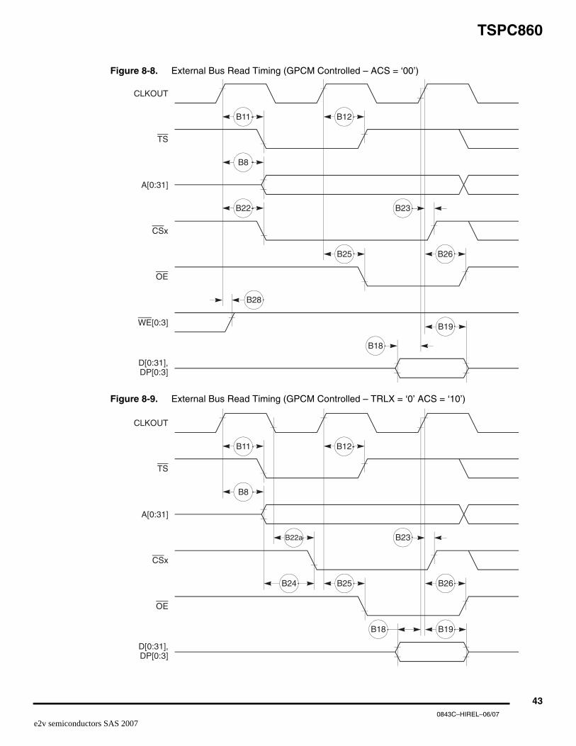
TSPC860
Figure 8-8. External Bus Read Timing (GPCM Controlled – ACS = ‘00’)
Figure 8-9. External Bus Read Timing (GPCM Controlled – TRLX = ‘0’ ACS = ‘10’)
CLKOUT
A[0:31]
CSx
OE
WE[0:3]
TS
D[0:31],DP[0:3]
B11 B12
B23
B8
B22
B26
B19
B18
B25
B28
CLKOUT
A[0:31]
CSx
OE
TS
D[0:31],DP[0:3]
B11 B12
B8
B22a B23
B26
B19B18
B25B24
430843C–HIREL–06/07
e2v semiconductors SAS 2007

TSPC860
Figure 8-10. External Bus Read Timing (GPCM Controlled – TRLX = ‘0’ ACS = ‘11’)
Figure 8-11. External Bus Read Timing (GPCM Controlled – TRLX = ‘1’, ACS = ‘10’, ACS = ‘11’)
CLKOUT
A[0:31]
CSx
OE
TS
D[0:31],DP[0:3]
B11 B12
B22bB8
B22c B23
B24a B25 B26
B19B18
CLKOUT
A[0:31]
CSx
OE
TS
D[0:31],DP[0:3]
B11 B12
B8
B22a
B27
B27a
B22b B22c B19B18
B26
B23
440843C–HIREL–06/07
e2v semiconductors SAS 2007

TSPC860
Figure 8-12. External Bus Write Timing (GPCM controlled – TRLX = ‘0’, CSNT = ‘0’)
CLKOUT
A[0:31]
CSx
WE[0:3]
OE
TS
D[0:31],DP[0:3]
B11
B8
B22 B23
B12
B30
B28B25
B26
B8 B9
B29
B29b
450843C–HIREL–06/07
e2v semiconductors SAS 2007

TSPC860
Figure 8-13. External Bus Write Timing (GPCM controlled – TRLX = ‘0’, CSNT = ‘1’)
B23
B30a B30c
CLKOUT
A[0:31]
CSx
OE
WE[0:3]
TS
D[0:31],DP[0:3]
B11
B8
B22
B12
B28b B28d
B25
B26
B8
B28a
B9
B28c
B29c B29g
B29a B29f
460843C–HIREL–06/07
e2v semiconductors SAS 2007

TSPC860
Figure 8-14. External Bus Write Timing (GPCM controlled – TRLX = ‘1’, CSNT = ‘1’)
B23B22
B8
B12B11
CLKOUT
A[0:31]
CSx
WE[0:3]
TS
OE
D[0:31],DP[0:3]
B30dB30b
B28b B28d
B25 B29e B29i
B26 B29d B29h
B28a B28c B9B8
B29b
470843C–HIREL–06/07
e2v semiconductors SAS 2007

TSPC860
Figure 8-15. External Bus Timing (UPM Controlled Signals)
Figure 8-16. Asynchronous UPWAIT Asserted Detection in UPM Handled Cycles Timing
CLKOUT
CSx
B31d
B8
B31
B34
B32b
GPL_A[0:5],GPL_B[0:5]
BS_A[0:3],BS_B[0:3]
A[0:31]
B31c
B31b
B34a
B32
B32a B32d
B34b
B36
B35b
B35a
B35
B33
B32c
B33a
B31a
CLKOUT
CSx
UPWAIT
GPL_A[0:5],GPL_B[0:5]
BS_A[0:3],BS_B[0:3]
B37
B38
480843C–HIREL–06/07
e2v semiconductors SAS 2007

TSPC860
Figure 8-17. Asynchronous UPWAIT Negated Detection in UPM Handled Cycles Timing
Figure 8-18. Synchronous External Master Access Timing – GPCM handled ACS = ‘00’
CLKOUT
CSx
UPWAIT
GPL_A[0:5],GPL_B[0:5]
BS_A[0:3],BS_B[0:3]
B37
B38
CLKOUT
TS
A[0:31],TSIZ[0:1],
R/W, BURST
CSx
B41 B42
B40
B22
490843C–HIREL–06/07
e2v semiconductors SAS 2007

TSPC860
Figure 8-19. Asynchronous External Master Memory Access Timing (GPCM Controlled – ACS = ’00’)
Figure 8-20. Asynchronous External Master – Control Signals Negation Time
Notes: 1. The timings I39 and I40 describe the testing conditions under which the IRQ lines are tested when being defined as level sensitive. The IRQ lines are synchronized internally and do not have to be asserted or negated with reference to the CLK-OUT.The timings I41, I42 and I43 are specified to allow the correct function of the IRQ lines detection circuitry, and has no direct relation with the total system interrupt latency that the TSPC860 is able to support.
CLKOUT
AS
A[0:31],TSIZ[0:1],
R/W
CSx
B39
B40
B22
AS
B43
CSx, WE[0:3],OE, GPLx,BS[0:3]
Table 8-3. Interrupt Timing
Number Characteristic(1)
All Frequencies
UnitMin Max
I39 IRQx Valid to CLKOUT Rising Edge (Set Up Time) 6 – ns
I40 IRQx Hold Time After CLKOUT 2 – ns
I41 IRQx Pulse Width Low 3 – ns
I42 IRQx Pulse Width High 3 – ns
I43 IRQx Edge to Edge Time 4 × TCLOCKOUT – –
500843C–HIREL–06/07
e2v semiconductors SAS 2007

TSPC860
Figure 8-21. Interrupt Detection Timing for External Level Sensitive Lines
Figure 8-22. Interrupt Detection Timing for External Edge Sensitive Lines
Notes: 1. PSST = 1. Otherwise add PSST times cycle time.
2. PSHT = 1. Otherwise add PSHT times cycle time.
CLKOUT
IRQx
I39
I40
CLKOUT
IRQx
I41 I42
I43
I43
Table 8-4. PCMCIA Timing
Num Characteristic
33 MHz 40 MHz 50 MHz 66 MHz
UnitMin Max Min Max Min Max Min Max
P44A(0:31), REG valid to PCMCIA Strobe asserted(1) 20.73 – 16.75 – 13 – 9.36 – ns
P45 A(0:31), REG valid to ALE negation(1) 28.30 – 23 – 18 – 13.15 – ns
P46 CLKOUT to REG valid 7.58 15.58 6.25 14.25 5 13 3.79 11.84 ns
P47 CLKOUT to REG Invalid 8.58 – 7.25 – 6 – 4.84 – ns
P48 CLKOUT to CE1, CE2 asserted 7.58 15.58 6.25 14.25 5 13 3.79 11.84
P49 CLKOUT to CE1, CE2 negated 7.58 15.58 6.25 14.25 5 13 3.79 11.84 ns
P50CLKOUT to PCOE, IORD, PCWE, IOWR assert time
11 11 ns
P51CLKOUT to PCOE, IORD, PCWE, IOWR negate time
2 11 2 11 ns
P52 CLKOUT to ALE assert time 7.58 15.58 6.25 14.25 5 13 3.79 11.04 ns
P53 CLKOUT to ALE negate time – 15.58 – 14.25 – 13 – 11.84 ns
P54 PCWE, IOWR negated to D(0:31) invalid(1) 5.58 – 4.25 – 3 – 1.79 – ns
P55WAITA and WAITB valid to CLKOUT rising edge(1) 8 – 8 – 8 – 8 – ns
P56CLKOUT rising edge to WAITA and WAITB invalid(1) 2 – 2 – 2 – 2 – ns
510843C–HIREL–06/07
e2v semiconductors SAS 2007

TSPC860
These synchronous timings define when the WAITx signals are detected in order to freeze (or relieve) the PCMCIA currentcycle. The WAITx assertion will be effective only if it is detected 2 cycles before the PSL timer expiration.
Figure 8-23. PCMCIA Access Cycles Timing External Bus Read
CLKOUT
A[0:31]
REG
CE1/CE2
PCOE, IORD
TS
D[0:31]
ALE
B19B18
P53P52 P52
P51P50
P48 P49
P46 P45
P44
P47
520843C–HIREL–06/07
e2v semiconductors SAS 2007
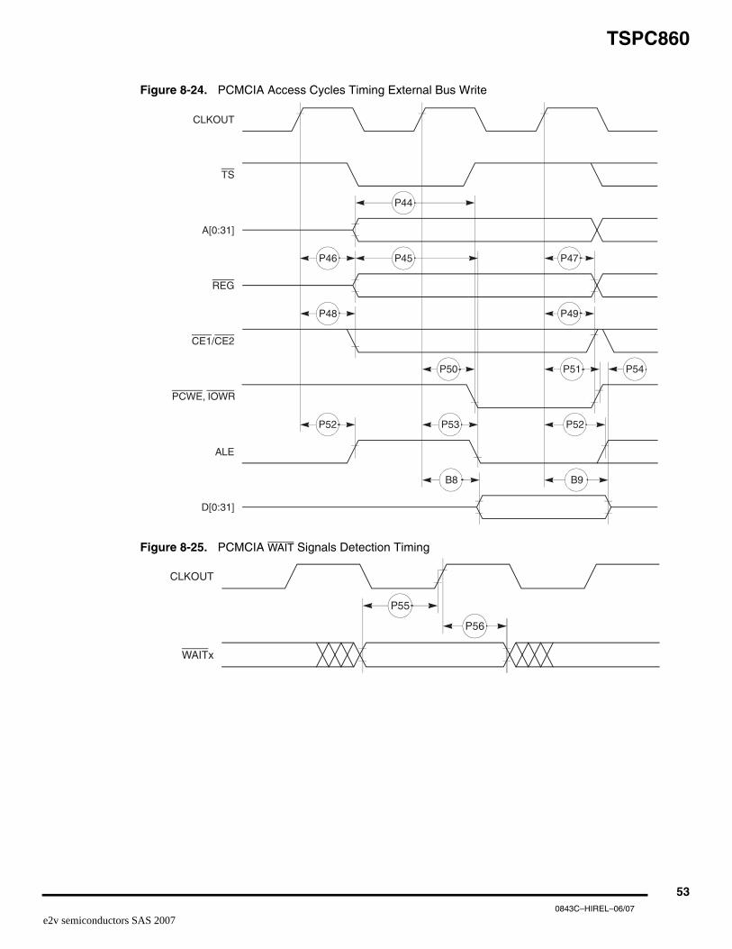
TSPC860
Figure 8-24. PCMCIA Access Cycles Timing External Bus Write
Figure 8-25. PCMCIA WAIT Signals Detection Timing
CLKOUT
A[0:31]
REG
CE1/CE2
PCWE, IOWR
TS
D[0:31]
ALE
B9B8
P53P52 P52
P51P50
P48 P49
P46 P45
P44
P47
P54
CLKOUT
WAITx
P55
P56
530843C–HIREL–06/07
e2v semiconductors SAS 2007

TSPC860
Note: 1. OP2 and OP3 only.
Figure 8-26. PCMCIA Output Port Timing
Figure 8-27. PCMCIA Input Port Timing
Table 8-5. PCMCIA Port Timing
Num Characteristic
33 MHz 40 MHz 50 MHz 66 MHz
UnitMin Max Min Max Min Max Min Max
P57 CLKOUT to OPx Valid – 19 – 19 – 19 – 19 ns
P58 HRESET negated to OPx drive(1) 25.73 – 21.75 – 18 – 14.36 – ns
P59 IP_Xx valid to CLKOUT Rising Edge 5 – 5 – 5 – 5 – ns
P60 CLKOUT Rising Edge to IP_Xx invalid 1 – 1 – 1 – 1 – ns
CLKOUT
HRESET
OutputSignals
OP2, OP3
P57
P58
CLKOUT
InputSignals
P59
P60
540843C–HIREL–06/07
e2v semiconductors SAS 2007
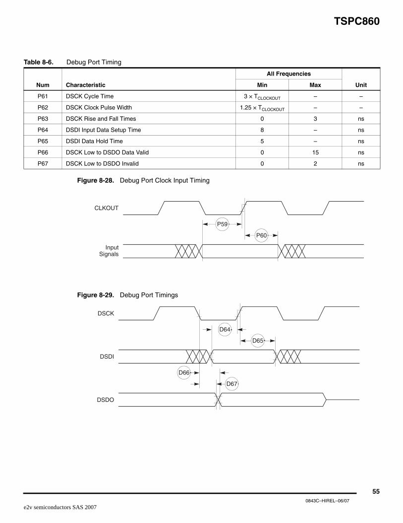
TSPC860
Figure 8-28. Debug Port Clock Input Timing
Figure 8-29. Debug Port Timings
Table 8-6. Debug Port Timing
Num Characteristic
All Frequencies
UnitMin Max
P61 DSCK Cycle Time 3 × TCLOCKOUT – –
P62 DSCK Clock Pulse Width 1.25 × TCLOCKOUT – –
P63 DSCK Rise and Fall Times 0 3 ns
P64 DSDI Input Data Setup Time 8 – ns
P65 DSDI Data Hold Time 5 – ns
P66 DSCK Low to DSDO Data Valid 0 15 ns
P67 DSCK Low to DSDO Invalid 0 2 ns
CLKOUT
InputSignals
P59
P60
DSCK
DSDI
DSDO
D64
D65
D66
D67
550843C–HIREL–06/07
e2v semiconductors SAS 2007

TSPC860
Figure 8-30. Reset Timing – Configuration from Data Bus
Table 8-7. RESET Timing
Num Characteristic
33 MHz 40 MHz 50 MHz 66 MHz
UnitMin Max Min Max Min Max Min Max
R69 CLKOUT to HRESET high impedance – 20 – 20 – 20 – 20 ns
R70 CLKOUT to SRESET high impedance – 20 – 20 – 20 – 20 ns
R71 RSTCONF pulse width 515.15 – 425 340 – 257.58 – ns
R72 – – – – – – – – – –
R73Configuration Data to HRESET rising edge set up time
504.55 – 425 – 350 – 277.27 – ns
R74Configuration Data to RSTCONF rising edge set up time
350 – 350 – 350 – 350 – ns
R75Configuration Data hold time after RSTCONF negation
0 – 0 – 0 – 0 – ns
R76Configuration Data hold time after HRESET negation
0 – 0 – 0 – 0 – ns
R77HRESET and RSTCONF asserted to Data out drive
– 25 – 25 – 25 – 25 ns
R78RSTCONF negated to Data out high impedance.
– 25 – 25 – 25 – 25 ns
R79CLKOUT of last rising edge before chip tristates HRESET to Data out high impedance.
– 25 – 25 – 25 – 25 ns
R80 DSDI, DSCK set up 90.91 – 75 – 60 – 45.45 – ns
R81 DSDI, DSCK hold time 0 – 0 – 0 – 0 – ns
R82SRESET negated to CLKOUT rising edge for DSDI and DSCK sample
242.42 – 200 – 160 – 121.21 – ns
HRESET
RSTCONF
D[0:31] (IN)
R71
R74
R73
R75
R76
560843C–HIREL–06/07
e2v semiconductors SAS 2007

TSPC860
Figure 8-31. Reset Timing – TSPC860 Data Bus Weak Drive during Configuration
Figure 8-32. Reset Timing – Debug Port Configuration IEEE 1149.1 Electrical Specifications
CLKOUT
HRESET
D[0:31] (OUT)(Weak)
RSTCONF
R69
R79
R77 R78
CLKOUT
SRESET
DSCK, DSDI
R70
R82
R80R80
R81 R81
Table 8-8. JTAG Timing
Num Characteristic
All Frequencies
UnitMin Max
J82 TCK Cycle Time 100 – ns
J83 TCK Clock Pulse Width Measured at 1.5V 40 – ns
J84 TCK Rise and Fall Times 0 10 ns
J85 TMS, TDI Data Setup Time 5 – ns
J86 TMS, TDI Data Hold Time 25 – ns
J87 TCK Low to TDO Data Valid – 27 ns
J88 TCK Low to TDO Data Invalid 0 – ns
J89 TCK low to TDO high impedance – 20 ns
J90 TRST Assert Time 100 – ns
J91 TRST Setup Time to TCK Low 40 – ns
570843C–HIREL–06/07
e2v semiconductors SAS 2007

TSPC860
Figure 8-33. JTAG Test Clock Input Timing
Figure 8-34. JTAG – Test Access Port Timing Diagram
Figure 8-35. JTAG – TRST Timing Diagram
J92 TCK Falling Edge to Output Valid – 50 ns
J93 TCK Falling Edge to Output Valid out of High Impedance – 50 ns
J94 TCK Falling Edge to Output High Impedance – 50 ns
J95 Boundary Scan Input Valid to TCK Rising Edge 50 – ns
J96 TCK Rising Edge to Boundary Scan Input Invalid 50 – ns
Table 8-8. JTAG Timing (Continued)
Num Characteristic
All Frequencies
UnitMin Max
TCK
J82 J83
J82 J83
J84 J84
TCK
TMS, TDI
TDO
J85
J86
J87
J88 J89
TCK
TRST
J91
J90
580843C–HIREL–06/07
e2v semiconductors SAS 2007

TSPC860
Figure 8-36. Boundary Scan (JTAG) Timing Diagram
9. CPM Electrical Characteristics
9.1 PIP/PIO AC Electrical Specifications
Note: 1. t3 = Specification 23
TCK
OutputSignals
OutputSignals
OutputSignals
J92 J94
J93
J95 J96
Table 9-1. PIP/PIO Timing
Num Characteristic
All Frequencies
UnitMin Max
21 Data-In Setup Time to STBI Low 0 – ns
22 Data-In Hold Time to STBI High 2.5 - t3(1) – clk
23 STBI Pulse Width 1.5 – clk
24 STBO Pulse Width 1 clk - 5 ns – ns
25 Data-Out Setup Time to STBO Low 2 – clk
26 Data-Out Hold Time from STBO High 5 – clk
27 STBI Low to STBO Low (Rx Interlock) – 2 clk
28 STBI Low to STBO High (Tx Interlock) 2 – clk
29 Data-In Setup Time to Clock Low 15 – ns
30 Data-In Hold Time from Clock Low 7.5 – ns
31 Clock High to Data-Out Valid (CPU Writes Data, Control, or Direction) – 25 ns
590843C–HIREL–06/07
e2v semiconductors SAS 2007

TSPC860
Figure 9-1. PIP RX (Interlock Mode) Timing Diagram
Figure 9-2. PIP TX (Interlock Mode) Timing Diagram
21
23
24
22
DATA IN
27
STBI
STBO
25
23
28
24 26
DATA OUT
STBO(OUTPUT)
STBI(INPUT)
600843C–HIREL–06/07
e2v semiconductors SAS 2007

TSPC860
Figure 9-3. PIP RX (Pulse Mode) Timing Diagram
Figure 9-4. PIP TX (Pulse Mode) Timing Diagram
21 22
23
24
DATA IN
STBI(INPUT)
STBO(OUTPUT)
25 26
24
23
DATA OUT
STBO(OUTPUT)
STBI(INPUT)
610843C–HIREL–06/07
e2v semiconductors SAS 2007

TSPC860
Figure 9-5. Parallel I/O Data-in/Data-out Timing Diagram
Note: 1. External bus frequency of greater than or equal to 33.34 MHz
Figure 9-6. Port C Interrupt Detection Timing
Table 9-2. Port C Interrupt Timing
Number Characteristic
≥ 33.34 MHz
UnitMin Max
35 Port C interrupt pulse width low (edge-triggered mode) 55 – ns
36 Port C interrupt minimum time between active edges 55 – ns
CLKO
DATA IN
DATA OUT
29
30
31
35
Port C(Input)
36
Table 9-3. IDMA Controller AC Electrical Specifications
Num Characteristic
All Frequencies
UnitMin Max
40 DREQ Setup Time to Clock High 7 – ns
41 DREQ Hold Time from Clock High 3 – ns
42 SDACK Assertion Delay from Clock High – 12 ns
43 SDACK Negation Delay from Clock Low – 12 ns
44 SDACK Negation Delay from TA Low – 20 ns
45 SDACK Negation Delay from Clock High – 15 ns
46 TA Assertion to Falling Edge of the Clock Setup Time (applies to external TA) 7 – ns
620843C–HIREL–06/07
e2v semiconductors SAS 2007

TSPC860
Figure 9-7. IDMA External Requests Timing Diagram
Figure 9-8. SDACK Timing Diagram – Peripheral Write, TA Sampled Low at the Falling Edge of the Clock
40
41
CLKO(OUTPUT)
DREQ(INPUT)
SDACK
CLKO(OUTPUT)
TS(OUTPUT)
RD/WR(OUTPUT)
DATA
TA(OUTPUT)
42 43
46
630843C–HIREL–06/07
e2v semiconductors SAS 2007

TSPC860
Figure 9-9. SDACK Timing Diagram – Peripheral Write, TA Sampled High at the Falling Edge of the Clock
Figure 9-10. SDACK Timing Diagram – Peripheral Read
42 44
CLKO(OUTPUT)
TS(OUTPUT)
RD/WR(OUTPUT)
DATA
TA(OUTPUT)
SDACK
42 45
CLKO(OUTPUT)
TS(OUTPUT)
RD/WR(OUTPUT)
DATA
TA(OUTPUT)
SDACK
640843C–HIREL–06/07
e2v semiconductors SAS 2007

TSPC860
Figure 9-11. Baud Rate Generator Timing Diagram
Figure 9-12. CPM General-Purpose Timers Timing Diagram
Table 9-4. Baud Rate Generator AC Electrical Specifications
Num Characteristic
All Frequencies
UnitMin Max
50 BRGO Rise and Fall Time – 10 ns
51 BRGO Duty Cycle 40 60 %
52 BRGO Cycle 40 – ns
51 51
BRGOx
52
5050
Table 9-5. Timer AC Electrical Specifications
Num Characteristic
All Frequencies
UnitMin Max
61 TIN/TGATE Rise and Fall Time 10 – ns
62 TIN/TGATE Low Time 1 – clk
63 TIN/TGATE High Time 2 – clk
64 TIN/TGATE Cycle Time 3 – clk
65 CLKO High to TOUT Valid 3 25 ns
CLKO
60
61
61
65
63 62
64
TIN/TGATE(INPUT)
TOUT(OUTPUT)
650843C–HIREL–06/07
e2v semiconductors SAS 2007

TSPC860
Notes: 1. The ratio SyncCLK/L1RCLK must be greater than 2.5/1.
2. Where P = 1/CLKOUT. Thus for a 25 MHz CLKO1 rate, P = 40 ns.
3. These specs are valid for IDL mode only.
4. The strobes and T × D on the first bit of the frame become valid after L1CLK edge or L1SYNC, whichever comes later.
Table 9-6. Serial Interface AC Electrical Specifications
Number Characteristic
All Frequencies
UnitMin Max
70 L1RCLK, L1TCLK Frequency (DSC = 0)(1)(3) – SYNCCLK/2.5 MHz
71 L1RCLK, L1TCLK Width Low (DSC = 0)(3) P+10 ns
71A L1RCLK, L1TCLK Width High (DSC = 0)(2) P+10 – ns
72 L1TXD, L1ST(1-4), L1RQ, L1CLKO Rise/Fall Time – 15 ns
73 L1RSYNC, L1TSYNC Valid to L1CLK Edge (SYNC Setup Time) 20 – ns
74 L1CLK Edge to L1RSYNC, L1TSYNC Invalid (SYNC Hold Time) 35 – ns
75 L1RSYNC, L1TSYNC Rise/Fall Time – 15 ns
76 L1RXD Valid to L1CLK Edge (L1RXD Setup Time) 17 – ns
77 L1CLK Edge to L1RXD Invalid (L1RXD Hold Time) 13 – ns
78 L1CLK Edge to L1ST(1-4) Valid(4) 10 45 ns
78A L1SYNC Valid to L1ST(1-4) Valid 10 45 ns
79 L1CLK Edge to L1ST(1-4) Invalid 10 45 ns
80 L1CLK Edge to L1TXD Valid 10 55 ns
80A L1TSYNC Valid to L1TXD Valid(4) 10 55 ns
81 L1CLK Edge to L1TXD High Impedance 0 42 ns
82 L1RCLK, L1TCLK Frequency (DSC = 1) – 16 or SYNCCLK/2 MHz
83 L1RCLK, L1TCLK Width Low (DSC = 1) P+10 – ns
83A L1RCLK, L1TCLK Width High (DSC = 1)(2) P+10 – ns
84 L1CLK Edge to L1CLKO Valid (DSC = 1) – 30 ns
85 L1RQ Valid Before Falling Edge of L1TSYNC(4) 1 – L1TCLK
86 L1GR Setup Time(3) 42 – ns
87 L1GR Hold Time 42 – ns
88L1CLK Edge to L1SYNC Valid (FSD = 00, CNT = 0000, BYT = 0, DSC = 0)
– 0 ns
660843C–HIREL–06/07
e2v semiconductors SAS 2007

TSPC860
Figure 9-13. SI Receive Timing Diagram with Normal Clocking (DSC = 0)
BIT 0
70
75
72
7374
76
77
71
78 79
RFSD =1
L1RCLK(FE = 0, CE = 0)
(Input)
L1ST(4-1)(Output)
71A
L1RCLK(FE = 1, CE = 1)
(Input)
L1RSYNC(Input)
L1RXD(Input)
670843C–HIREL–06/07
e2v semiconductors SAS 2007
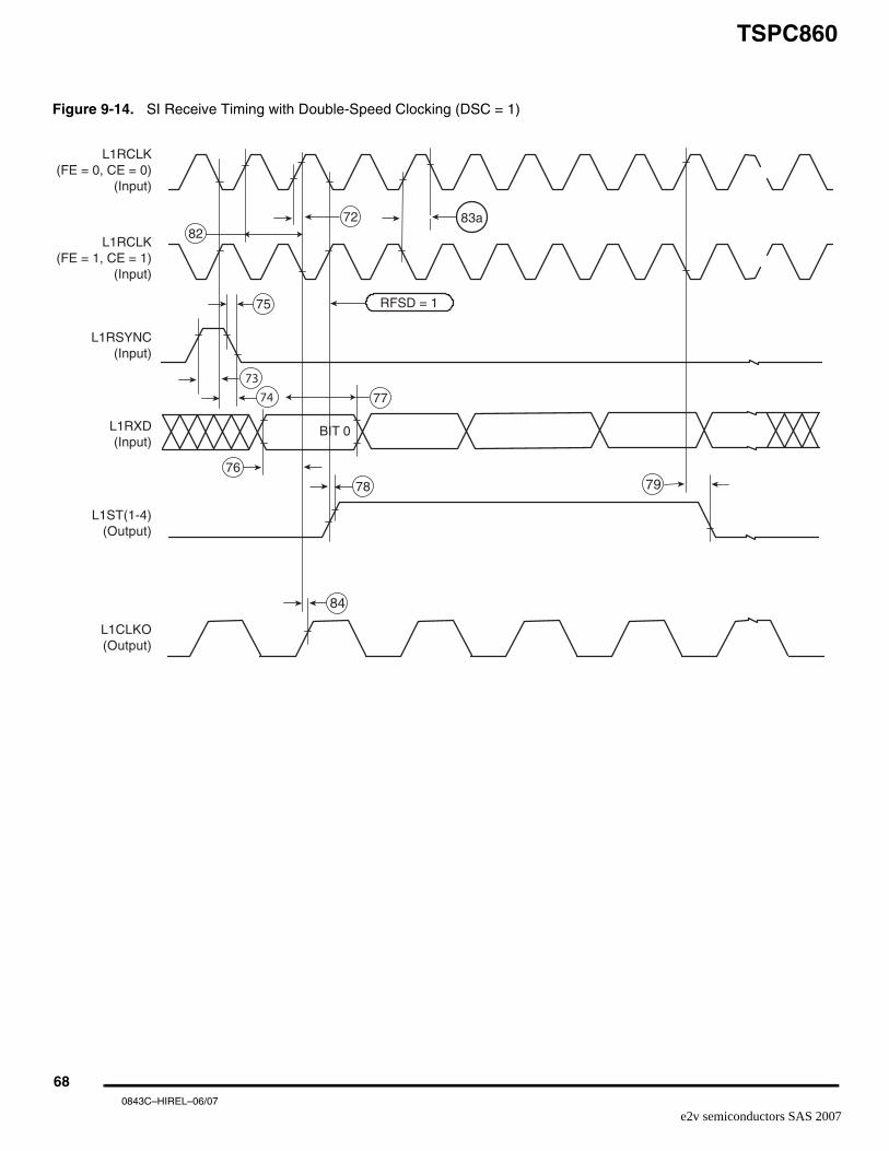
TSPC860
Figure 9-14. SI Receive Timing with Double-Speed Clocking (DSC = 1)
BIT 0
RFSD = 1
84
7978
76
83a
73
75
74 77
7282
L1RCLK(FE = 0, CE = 0)
(Input)
L1ST(1-4)(Output)
L1CLKO(Output)
L1RCLK(FE = 1, CE = 1)
(Input)
L1RSYNC(Input)
L1RXD(Input)
680843C–HIREL–06/07
e2v semiconductors SAS 2007
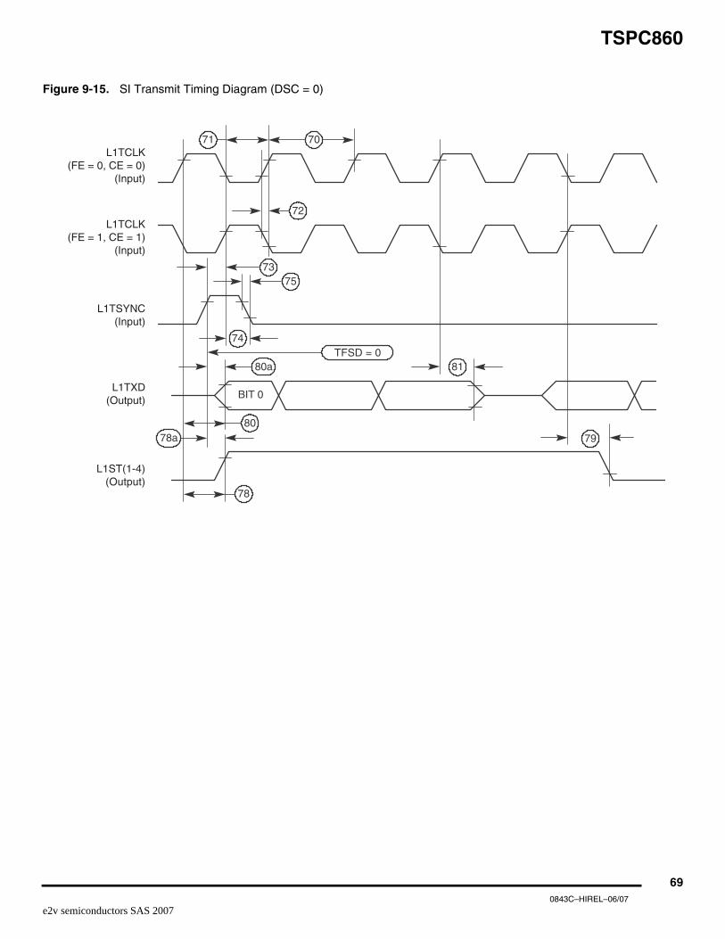
TSPC860
Figure 9-15. SI Transmit Timing Diagram (DSC = 0)
70
75
72
73
74
71
79
TFSD = 080a
BIT 0
80
78
81
78a
L1TCLK(FE = 0, CE = 0)
(Input)
L1ST(1-4)(Output)
L1TCLK(FE = 1, CE = 1)
(Input)
L1TSYNC(Input)
L1TXD(Output)
690843C–HIREL–06/07
e2v semiconductors SAS 2007
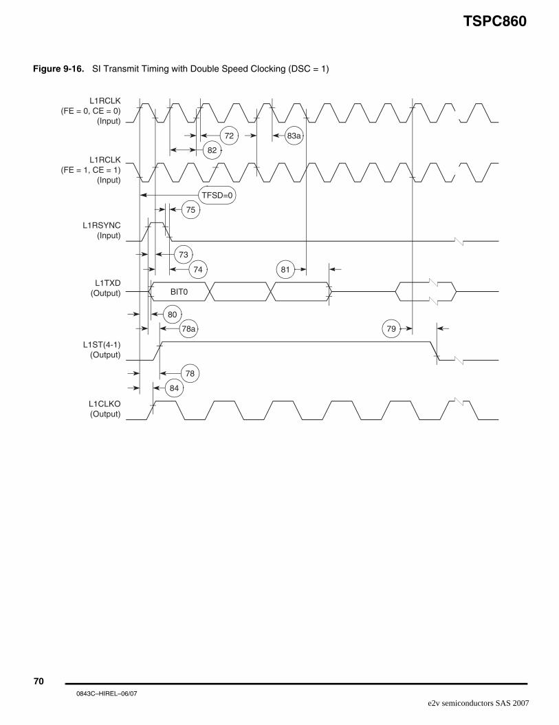
TSPC860
Figure 9-16. SI Transmit Timing with Double Speed Clocking (DSC = 1)
72
TFSD=0
75
73
74
78a
80
79
83a
82
84
BIT0
78
81
L1RCLK(FE = 0, CE = 0)
(Input)
L1ST(4-1)(Output)
L1CLKO(Output)
L1RCLK(FE = 1, CE = 1)
(Input)
L1RSYNC(Input)
L1TXD(Output)
700843C–HIREL–06/07
e2v semiconductors SAS 2007

e2v semiconductors SA
S 2007
TS
PC
860
Fig
ure 9-17.
IDL T
iming
B21 B20 D2 M
17 18 19 20
B21 B20 D2 M
710843C
–HIR
EL–06/07
B17 B16 B14 B13 B12 B11 B10 D1 A B27 B26 B25 B24 B23 B22B15L1RXD(Input)
L1TXD(Output)
L1ST(4-1)(Output)
L1RQ(Output)
73
77
1 2 3 4 5 6 7 8 9 10 11 12 13 14 15 16
74
80
B17 B16 B15 B14 B13 B12 B11 B10 D1 A B27 B26 B25 B24 B23 B22
71
71
L1GR(Input)
78
85
72
76
87
86
L1RSYNC(Input)
L1RCLK(Input)
81

TSPC860
9.2 SCC In NMSI Mode Electrical Specifications
Notes: 1. The ratio SyncCLK/RCLK1 and SyncCLK/TCLK1 must be greater or equal to 2.25/1.
2. Also applies to CD and CTS hold time when they are used as an external sync signals.
Notes: 1. The ratios SyncCLK/RCLK1 and SyncCLK/TCLK1 must be greater or equal to 3/1
2. Also applies to CD and CTS hold time when they are used as an external sync signals.
Table 9-7. NMSI External Clock Timing
Num Characteristic
All Frequencies
UnitMin Max
100 RCLK1 and TCLK1 Width High(1) 1/SYNCCLK – ns
101 RCLK1 and TCLK1 Width Low 1/SYNCCLK + 5 – ns
102 RCLK1 and TCLK1 Rise/Fall Time – 15 ns
103 TXD1 Active Delay (From TCLK1 Falling Edge) 0 50 ns
104 RTS1 Active/Inactive Delay (From TCLK1 Falling Edge) 0 50 ns
105 CTS1 Setup Time to TCLK1 Rising Edge 5 – ns
106 RXD1 Setup Time to RCLK1 Rising Edge 5 – ns
107 RXD1 Hold Time from RCLK1 Rising Edge(2) 5 – ns
108 CD1 Setup Time to RCLK1 Rising Edge 5 – ns
Table 9-8. NMSI Internal Clock Timing
Num Characteristic
All Frequencies
UnitMin Max
100 RCLK1 and TCLK frequency1(1) 0 SYNCCLK/3 MHz
102 RCLK1 and TCLK1 Rise/Fall Time – – ns
103 TXD1 Active Delay (From TCLK1 Falling Edge) 0 30 ns
104 RTS1 Active/Inactive Delay (From TCLK1 Falling Edge) 0 30 ns
105 CTS1 Setup Time to TCLK1 Rising Edge 40 – ns
106 RXD1 Setup Time to RCLK1 Rising Edge 40 – ns
107 RXD1 Hold Time from RCLK1 Rising Edge(2) 0 – ns
108 CD1 Setup Time to RCLK1 Rising Edge 40 – ns
720843C–HIREL–06/07
e2v semiconductors SAS 2007

TSPC860
Figure 9-18. SCC NMSI Receive Timing Diagram
Figure 9-19. SCC NMSI Transmit Timing Diagram
101
100
107
108
106
RCLK1
RXD1(INPUT)
107
CD1(INPUT)
CD1(SYNCINPUT)
102102
100
107
105
103
104 104
102
102 101
TCLK1
TXD1(OUTPUT)
RTS1(OUTPUT)
CTS1(INPUT)
CTS1(SYNCINPUT)
730843C–HIREL–06/07
e2v semiconductors SAS 2007

TSPC860
Figure 9-20. HDLC Bus Timing Diagram
100
105
TCLK1
TXD1(OUTPUT)
103
104
104
RTS1(OUTPUT)
102
102 101
CTS1(ECHOINPUT)
107
Table 9-9. Ethernet Electrical Specifications
Number Characteristic
All Frequencies
UnitMin Max
120 CLSN Width High 40 – ns
121 RCLK1 Rise/Fall Time – 15 ns
122 RCLK1 Width Low 40 – ns
123 RCLK1 Clock Period(1) 80 120 ns
124 RXD1 Setup Time 20 – ns
125 RXD1 Hold Time 5 – ns
126 RENA Active Delay (From RCLK1 Rising Edge of the Last Data Bit) 10 – ns
127 RENA Width Low 100 – ns
128 TCLK1 Rise/Fall Time – 15 ns
129 TCLK1 Width Low 40 – ns
130 TCLK1 Clock Period(1) 99 101 ns
131 TXD1 Active Delay (From TCLK1 Rising Edge) 10 50 ns
132 TXD1 Inactive Delay (From TCLK1 Rising Edge) 10 50 ns
133 TENA Active Delay (From TCLK1 Rising Edge) 10 50 ns
134 TENA Inactive Delay (From TCLK1 Rising Edge) 10 50 ns
135 RSTRT Active Delay (From TCLK1 Falling Edge) 10 50 ns
136 RSTRT Inactive Delay (From TCLK1 Falling Edge) 10 50 ns
137 REJECT Width Low 1 – CLK
138 CLKO1 Low to SDACK Asserted(2) – 20 ns
139 CLKO1 Low to SDACK Negated(2) – 20 ns
740843C–HIREL–06/07
e2v semiconductors SAS 2007

TSPC860
Notes: 1. The ratio SyncCLK/RCLK1 and SyncCLK/TCLK1 must be greater or equal to 2/1
2. SDACK is asserted whenever the SDMA writes the incoming frame DA into memory.
Figure 9-21. Ethernet Collision Timing Diagram
Figure 9-22. Ethernet Receive Timing Diagram
Figure 9-23. Ethernet Transmit Timing Diagram
Notes: 1. Transmit clock invert (TCI) bit in GSMR is set.
2. If RENA is deasserted before TENA, or RENA is not asserted at all during transmit, then the CSL bit is set in the buffer descriptor at the end of the frame transmission.
120
CLSN (CTS1)(Input)
RCLK1
RXD1(INPUT)
RENA (CD1)(INPUT)
121
124
125127
123
126
LAST BIT
121
128
121132131
133 134
129
TCLK1
TXD1(Output)
RENA (CD1)(Input)
(Note 2)
TENA (RTS1)(Input)
128
750843C–HIREL–06/07
e2v semiconductors SAS 2007

TSPC860
Figure 9-24. CAM Interface Receive Start Timing Diagram
Figure 9-25. CAM Interface REJECT Timing Diagram
Note: 1. The ratio SYNCCLK/SMCLK must be greater or equal to 2/1.
0 1 1 bit #1 bit #2
START FRAME125
136
RCLK1
RXD1(Input)
RSTRT(Output)
137
Table 9-10. SMC Transparent AC Electrical specifications
Number Characteristic
All Frequencies
UnitMin Max
150 SMCLK Clock Period(1) 100 – ns
151 SMCLK Width Low 50 – ns
151A SMCLK Width High 50 – ns
152 SMCLK Rise/Fall Time – 15 ns
153 SMTXD active delay (from SMCLK falling edge) 10 50 ns
154 SMRXD/SMSYNC setup time 20 – ns
155 RXD1/SMSYNC1 Hold Time 5 – ns
760843C–HIREL–06/07
e2v semiconductors SAS 2007
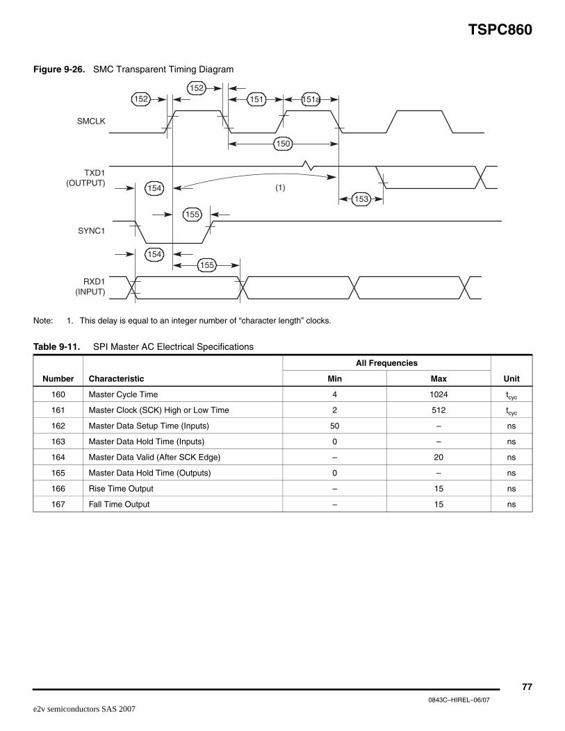
TSPC860
Figure 9-26. SMC Transparent Timing Diagram
Note: 1. This delay is equal to an integer number of “character length” clocks.
150
151 151a152
154
155
155
153(1)
SMCLK
TXD1(OUTPUT)
SYNC1
RXD1(INPUT)
152
154
Table 9-11. SPI Master AC Electrical Specifications
Number Characteristic
All Frequencies
UnitMin Max
160 Master Cycle Time 4 1024 tcyc
161 Master Clock (SCK) High or Low Time 2 512 tcyc
162 Master Data Setup Time (Inputs) 50 – ns
163 Master Data Hold Time (Inputs) 0 – ns
164 Master Data Valid (After SCK Edge) – 20 ns
165 Master Data Hold Time (Outputs) 0 – ns
166 Rise Time Output – 15 ns
167 Fall Time Output – 15 ns
770843C–HIREL–06/07
e2v semiconductors SAS 2007

TSPC860
Figure 9-27. SPI Master (CP = 0) Timing Diagram
Figure 9-28. SPI Master (CP = 1) Timing Diagram
SPICLKCi = 0
OUTPUT
msb data lsb msb
162
167
163
165164
166
166167
167
166
161
MSB data LSB MSB
160161
SPIMISOINPUT
SPIMOSIOUTPUT
SPICLKCi = 1
OUTPUT
162
167
163
165164
166
166167
167
166
161
160161
msb data lsb msb
MSB data LSB MSB
SPICLKCi = 0
OUTPUT
SPIMISOINPUT
SPIMOSIOUTPUT
SPICLKCi = 1
OUTPUT
780843C–HIREL–06/07
e2v semiconductors SAS 2007

TSPC860
Figure 9-29. SPI Slave (CP = 0) Timing Diagram
Table 9-12. SPI Slave AC Electrical Specifications
Number Characteristic
All Frequencies
UnitMin Max
170 Slave Cycle Time 2 – tcyc
171 Slave Enable Lead Time 15 – ns
172 Slave Enable Lag Time 15 – ns
173 Slave Clock (SPICLK) High or Low Time 1 – tcyc
174Slave Sequential Transfer Delay (Does Not Require Deselect)
1 – tcyc
175 Slave Data Setup Time (Inputs) 20 – ns
176 Slave Data Hold Time (Inputs) 20 – ns
177 Slave Access Time – 50 ns
181182
181
173170173
177180
181
182178
179175176
182
171172
174
DATA
DATA
UNDEF
LSBIN MSBIN
MSBOUTLSBOUT
MSBIN
MSBOUT
SPICLKCi = 0
INPUT
SPICLKCi = 1
INPUT
SPISELINPUT
SPIMISOOUTPUT
SPIMOSIINPUT
790843C–HIREL–06/07
e2v semiconductors SAS 2007
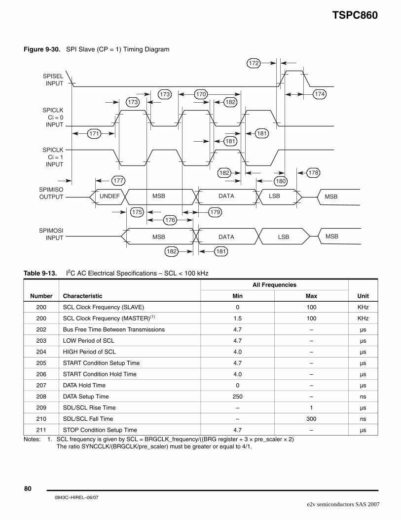
TSPC860
Figure 9-30. SPI Slave (CP = 1) Timing Diagram
Notes: 1. SCL frequency is given by SCL = BRGCLK_frequency/((BRG register + 3 × pre_scaler × 2)The ratio SYNCCLK/(BRGCLK/pre_scaler) must be greater or equal to 4/1.
SPICLKCi = 0
INPUT
SPICLKCi = 1
INPUT
UNDEF
170 174
172
182
181
173173
171181
177
179
178182180
175176
181182
SPISELINPUT
SPIMISOOUTPUT
SPIMOSIINPUT
DATA
DATA LSB
LSB MSB
MSB
MSB
MSB
Table 9-13. I2C AC Electrical Specifications – SCL < 100 kHz
Number Characteristic
All Frequencies
UnitMin Max
200 SCL Clock Frequency (SLAVE) 0 100 KHz
200 SCL Clock Frequency (MASTER)(1) 1.5 100 KHz
202 Bus Free Time Between Transmissions 4.7 – µs
203 LOW Period of SCL 4.7 – µs
204 HIGH Period of SCL 4.0 – µs
205 START Condition Setup Time 4.7 – µs
206 START Condition Hold Time 4.0 – µs
207 DATA Hold Time 0 – µs
208 DATA Setup Time 250 – ns
209 SDL/SCL Rise Time – 1 µs
210 SDL/SCL Fall Time – 300 ns
211 STOP Condition Setup Time 4.7 – µs
800843C–HIREL–06/07
e2v semiconductors SAS 2007
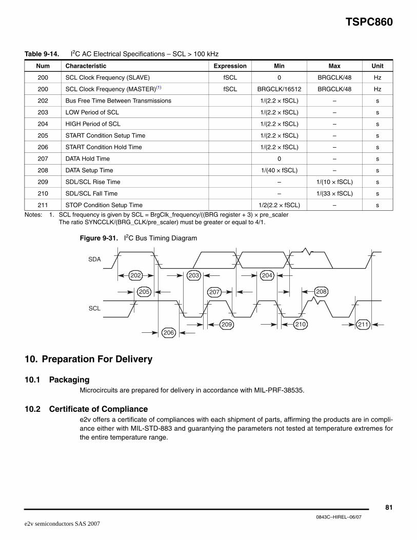
TSPC860
Notes: 1. SCL frequency is given by SCL = BrgClk_frequency/((BRG register + 3) × pre_scaler The ratio SYNCCLK/(BRG_CLK/pre_scaler) must be greater or equal to 4/1.
Figure 9-31. I2C Bus Timing Diagram
10. Preparation For Delivery
10.1 PackagingMicrocircuits are prepared for delivery in accordance with MIL-PRF-38535.
10.2 Certificate of Compliancee2v offers a certificate of compliances with each shipment of parts, affirming the products are in compli-ance either with MIL-STD-883 and guarantying the parameters not tested at temperature extremes forthe entire temperature range.
Table 9-14. I2C AC Electrical Specifications – SCL > 100 kHz
Num Characteristic Expression Min Max Unit
200 SCL Clock Frequency (SLAVE) fSCL 0 BRGCLK/48 Hz
200 SCL Clock Frequency (MASTER)(1) fSCL BRGCLK/16512 BRGCLK/48 Hz
202 Bus Free Time Between Transmissions 1/(2.2 × fSCL) – s
203 LOW Period of SCL 1/(2.2 × fSCL) – s
204 HIGH Period of SCL 1/(2.2 × fSCL) – s
205 START Condition Setup Time 1/(2.2 × fSCL) – s
206 START Condition Hold Time 1/(2.2 × fSCL) – s
207 DATA Hold Time 0 – s
208 DATA Setup Time 1/(40 × fSCL) – s
209 SDL/SCL Rise Time – 1/(10 × fSCL) s
210 SDL/SCL Fall Time – 1/(33 × fSCL) s
211 STOP Condition Setup Time 1/2(2.2 × fSCL) – s
202
SDA
SCL
203 204
205 207 208
209206
210 211
810843C–HIREL–06/07
e2v semiconductors SAS 2007

TSPC860
11. Power ConsiderationThe average chip-junction temperature, Tj, in °C can be obtained from the equation:
Tj = TA + (PD · ΟJA) (1)
where
TA = Ambient temperature, °C
ΟJA = Package thermal resistance, junction to ambient, °C/W
PD = PINT + PI/O
PINT = IDD × VDD, watts – chip internal power
PI/O = Power dissipation on input and output pins – user determined
For most applications PI/O < 0.3 · PINT and can be neglected. If PI/O is neglected, an approximate relation-ship between PD and TJ is:
PD = K ÷ (TJ + 273°C) (2)
Solving equations (1) and (2) for K gives:
K = PD · T (TA + 273°C) + ΟJA · PD2 (3)
where K is a constant pertaining to the particular part. K can be determined from equation (3) by measur-ing PD (at equilibrium) for a known TA. Using this value of K, the values of PD and TJ can be obtained bysolving equations (1) and (2) iteratively for any value of TA.
11.1 Layout PracticesEach VDD pin on the TSPC860 should be provided with a low-impedance path to the board’s supply.Each GND pin should likewise be provided with a low-impedance path to ground. The power supply pinsdrive distinct groups of logic on chip. The VDD power supply should be bypassed to ground using at leastfour 0.1 µF bypass capacitors located as close as possible to the four sides of the package. The capaci-tor leads and associated printed circuit traces connecting to chip VDD and GND should be kept to lessthan half an inch per capacitor lead. A four-layer board, employing two inner layers as VDD and GNDplanes is recommended.
All output pins on the TSPC860 have fast rise and fall times. Printed circuit (PC) trace interconnectionlength should be minimized in order to minimize undershoot and reflections caused by these fast outputswitching times. This recommendation particularly applies to the address and data busses. MaximumPC trace lengths of six inches are recommended. Capacitance calculations should consider all deviceloads as well as parasitic capacitances due to the PC traces. Attention to proper PCB layout and bypass-ing becomes especially critical in systems with higher capacitive loads because these loads createhigher transient current in the VDD and GND circuits. Pull up all unused inputs or signals that will beinputs during reset. Special care should be taken to minimize the noise levels on the PLL supply pins.
12. Functional Units DescriptionThe TSPC860 PowerQUICC integrates the Embedded PowerPC Core with high performance, low powerperipherals to extend the Freescale Data Communications family of embedded processors even fartherinto high end communications and networking products.The TSPC860 PowerQUICC is comprised of three modules which all use the 32-bit internal bus: theEmbedded PowerPC Core, the System Integration Unit (SIU), and the Communication Processor Mod-ule (CPM). The TSPC860 PowerQUICC block diagram is shown in Figure 1-1.
820843C–HIREL–06/07
e2v semiconductors SAS 2007

TSPC860
12.1 Embedded PowerPC CoreThe Embedded PowerPC Core is compliant with the Book 1 specification for the PowerPC architecture.The Embedded PowerPC Core is a fully static design that consists of two functional blocks; the integerblock and the load/store block. It executes all integer and load/store operations directly on the hardware.The core supports integer operations on a 32-bit internal data path and 32-bit arithmetic hardware. Thecore interface to the internal and external buses is 32 bits. The core uses a two instruction load/storequeue, a four instruction prefetch queue, and a six instruction history buffer. The core does branch fold-ing and branch prediction with conditional pre-fetch but without conditional execution. The EmbeddedPowerPC Core can operate on 32-bit external operands with one bus cycle.
The PowerPC integer block supports 32 × 32-bit fixed point general purpose registers. It can executeone integer instruction each clock cycle. Each element in the integer block is clocked only when validdata is present in the data queue ready for operation. This assures that the power consumption of thedevice is held to the absolute minimum required to perform an operation.
The Embedded PowerPC Core is integrated with MMU’s as well as 4 kbyte instruction and data caches.Each MMU provides a 32 entry, fully associative instruction and data TLB, with multiple page sizes of: 4KB, 16 KB, 512 KB, 256 KB and 8 MB. It will support 16 virtual address spaces with 8 protection groups.Three special registers are available as scratch registers to support software table walk and update.Theinstruction cache is 4 kilobytes, two-way, set associative with physical addressing. It allows single cycleaccess on hit with no added latency for miss. It has four words per line, supporting burst line fill usingLeast Recently Used (LRU) replacement. The cache can be locked on a per line basis for applicationcritical routines.
The data cache is 4 kilobytes, two-way, set associative with physical addressing. It allows single cycleaccess on hit with one added clock latency for miss. It has four words per line, supporting burst line fillusing LRU replacement. The cache can be locked on a per line basis for application critical routines. Thedata cache can be programmed to support copy-back or write-through via the MMU. The inhibit modecan be programmed per MMU page.
The Embedded PowerPC Core with its Instruction and data caches delivers approximately 52 MIPS at40 MHz, using Dhrystone 2.1, based on the assumption that it is issuing one instruction per cycle with acache hit rate of 94%.
The Embedded PowerPC Core contains a much improved debug interface that provides superior debugcapabilities without causing any degradation in the speed of operation. This interface supports six watch-point pins that are used to detect software events. Internally it has eight comparators, four of whichoperate on the effective address on the address bus. The remaining four comparators are split, with twocomparators the effective address on the data bus, and two comparators operating on the data on thedata bus. The Embedded PowerPC Core can compare using =, ≠, <, > conditions to generate watch-points. Each watchpoint can then generate a breakpoint that can be programmed to trigger in aprogrammable number of events.
12.2 System Interface Unit (SIU)The SIU on the TSPC860 PowerQUICC integrates general-purpose features useful in almost any 32-bitprocessor system, enhancing the performance provided by the system integration module (SIM) on theTS68EN360 QUICC device.
Although the Embedded PowerPC Core is always a 32-bit device internally, it may be configured to oper-ate with an 8-, 16- or 32-bit data bus. Regardless of the choice of the system bus size, dynamic bussizing is supported. Bus sizing allows 8-, 16-, and 32-bit peripherals and memory to exist in the 32-bitsystem bus mode.
830843C–HIREL–06/07
e2v semiconductors SAS 2007
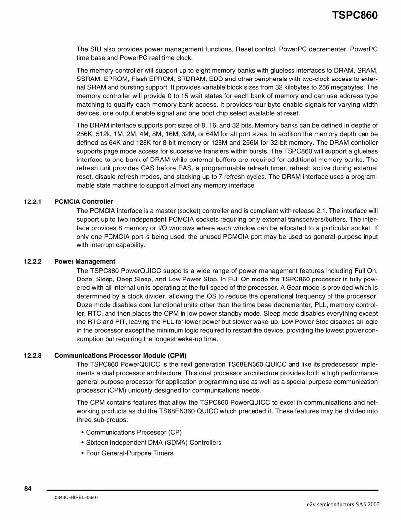
TSPC860
The SIU also provides power management functions, Reset control, PowerPC decrementer, PowerPCtime base and PowerPC real time clock.
The memory controller will support up to eight memory banks with glueless interfaces to DRAM, SRAM,SSRAM, EPROM, Flash EPROM, SRDRAM, EDO and other peripherals with two-clock access to exter-nal SRAM and bursting support. It provides variable block sizes from 32 kilobytes to 256 megabytes. Thememory controller will provide 0 to 15 wait states for each bank of memory and can use address typematching to qualify each memory bank access. It provides four byte enable signals for varying widthdevices, one output enable signal and one boot chip select available at reset.
The DRAM interface supports port sizes of 8, 16, and 32 bits. Memory banks can be defined in depths of256K, 512k, 1M, 2M, 4M, 8M, 16M, 32M, or 64M for all port sizes. In addition the memory depth can bedefined as 64K and 128K for 8-bit memory or 128M and 256M for 32-bit memory. The DRAM controllersupports page mode access for successive transfers within bursts. The TSPC860 will support a gluelessinterface to one bank of DRAM while external buffers are required for additional memory banks. Therefresh unit provides CAS before RAS, a programmable refresh timer, refresh active during externalreset, disable refresh modes, and stacking up to 7 refresh cycles. The DRAM interface uses a program-mable state machine to support almost any memory interface.
12.2.1 PCMCIA ControllerThe PCMCIA interface is a master (socket) controller and is compliant with release 2.1. The interface willsupport up to two independent PCMCIA sockets requiring only external transceivers/buffers. The inter-face provides 8 memory or I/O windows where each window can be allocated to a particular socket. Ifonly one PCMCIA port is being used, the unused PCMCIA port may be used as general-purpose inputwith interrupt capability.
12.2.2 Power ManagementThe TSPC860 PowerQUICC supports a wide range of power management features including Full On,Doze, Sleep, Deep Sleep, and Low Power Stop. In Full On mode the TSPC860 processor is fully pow-ered with all internal units operating at the full speed of the processor. A Gear mode is provided which isdetermined by a clock divider, allowing the OS to reduce the operational frequency of the processor.Doze mode disables core functional units other than the time base decrementer, PLL, memory control-ler, RTC, and then places the CPM in low power standby mode. Sleep mode disables everything exceptthe RTC and PIT, leaving the PLL for lower power but slower wake-up. Low Power Stop disables all logicin the processor except the minimum logic required to restart the device, providing the lowest power con-sumption but requiring the longest wake-up time.
12.2.3 Communications Processor Module (CPM)The TSPC860 PowerQUICC is the next generation TS68EN360 QUICC and like its predecessor imple-ments a dual processor architecture. This dual processor architecture provides both a high performancegeneral purpose processor for application programming use as well as a special purpose communicationprocessor (CPM) uniquely designed for communications needs.
The CPM contains features that allow the TSPC860 PowerQUICC to excel in communications and net-working products as did the TS68EN360 QUICC which preceded it. These features may be divided intothree sub-groups:
• Communications Processor (CP)
• Sixteen Independent DMA (SDMA) Controllers
• Four General-Purpose Timers
840843C–HIREL–06/07
e2v semiconductors SAS 2007

TSPC860
The CP provides the communication features of the TSPC860 PowerQUICC. Included are a RISC pro-cessor, four Serial Communication Controllers (SCC) four Serial Management Controllers (SMC), oneSerial Peripheral Interface (SPI), one I2 Interface, 5 kilobytes of dual-port RAM, an interrupt controller, atime slot assigner, three parallel ports, a parallel interface port, four independent baud rate generators,and sixteen serial DMA channels to support the SCCs, SMCs, SPI, and I2C.
The SDMAs provide two channels of general-purpose DMA capability for each communications channel.They offer high-speed transfers, 32-bit data movement, buffer chaining, and independent request andacknowledge logic.
The four general-purpose timers on the CPM are identical to the timers found on the MC68360 and stillsupport the internal cascading of two timers to form a 32-bit timer.The TSPC860 PowerQUICC maintains the best features of the TS68EN360 QUICC, while makingchanges required to provide for the increased flexibility, integration, and performance requested by cus-tomers demanding the performance of the powerPC architecture. The addition of a Multiply-And-Accumulate (MAC) function on the CPM further enhances the TSPC860 PowerQUICC, enabling variousmodem and DSP applications. Because the CPM architectural approach remains intact between theTSPC860 PowerQUICC and the TS68EN360 QUICC, a user of the TS68EN360 QUICC can easilybecome familiar with the TSPC860 PowerQUICC.
12.3 Software Compatibility IssuesThe following list summarizes the major software differences between the TS68EN360 QUICC and theTSPC860 PowerQUICC:
• Since the TSPC860 PowerQUICC uses an Embedded PowerPC Core, code written for the TS68EN360 must be recompiled for the PowerPC instruction set. Code which accesses the TS68EN360 peripherals requires only minor modifications for use with the TSPC860. Although the functions performed by the PowerQUICC SIU are similar to those performed by the QUICC SIM, the initialization sequence for the SIU is different and therefore code that accesses the SIU must be rewritten. Many developers of 68K compilers now provide compilers which also support the PowerPC architecture.
• The addition of the MAC function to the TSPC860 CPM block to support the needs of higher performance communication software is the only major difference between the CPM on the TS68EN360 and that on the TSPC860. Therefore the registers used to initialize the QUICC CPM are similar to the TSPC860 CPM, but there are some minor changes necessary for supporting the MAC function.
• When porting code from the TS68EN360 CPM to the TSPC860 CPM, the software writer will find new options for hardware breakpoint on CPU commands, address, and serial request which are useful for software debugging. Support for single step operation with all the registers of the CPM visible makes software development for the CPM on the TSPC860 processor even simpler.
850843C–HIREL–06/07
e2v semiconductors SAS 2007

TSPC860
12.4 TSPC860 PowerQUICC Glueless System DesignA fundamental design goal of the TSPC860 PowerQUICC was ease of interface to other system compo-nents. Figure 10-30 on page 80 shows a system configuration that offers one EPROM, one flashEPROM, and supports two DRAM SIMMs. Depending on the capacitance on the system bus, externalbuffers may be required. From a logic standpoint, however, a glueless system is maintained.
Figure 12-1. TSPC860 System Configuration
13. Preparation for Delivery
13.1 MarkingEach microcircuit is legible and permanently marked with the following information at minimum:
• e2v logo
• Manufacturer’s part number
• Class B identification if applicable
• Date-code of inspection lot
• ESD identifier if available
• Country of manufacturing
13.2 PackagingMicrocircuits are prepared for delivery in accordance with MIL-PRF-38535.
Buffer
PRTY[3-0]
RASCAS[3-0]W (write)DataAddressParity
RASRAS2
RAS1 CAS[3-0]
PowerQUICCPC860
CS0OE
DataAddress
CS7
WE[3-0]
CE (Enable) OE (Output Enable)WE (Write)DataAddress
8-bit bootEPROM
(Flash or Regular)
E (Enable)G (Output Enable)W (Write)DataAddress
16 or 32 BitTwo DRAM SIMMs
(Optional Parity)
8, 16 or 32-bit SRAM
860843C–HIREL–06/07
e2v semiconductors SAS 2007

TSPC860
13.3 Certificate of Compliancee2v offers a certificate of compliances with each shipment of parts, affirming the products are in compli-ance either with MIL-STD-883 and guarantying the parameters not tested at temperature extremes forthe entire temperature range.
13.4 HandlingMOS devices must be handled with certain precautions to avoid damage due to accumulation of staticcharge. Input protection devices have been designed in the chip to minimize the effect of this staticbuildup. However, the following handling practices are recommended:
a) Devices should be handled on benches with conductive and grounded surfaces
b) Ground test equipment, tools and operator
c) Do not handle devices by the leads
d) Store devices in conductive foam or carriers
e) Avoid use of plastic, rubber, or silk in MOS areas
f) Maintain relative humidity above 50% if practical
14. Package Mechanical Data
14.1 Package ParametersThe TSPC860 uses a 25 mm × 25 mm, 357 pin Plastic Ball Grid Array (PBGA) package. The plasticpackage parameters are as provided in the following list.
Package Outline 25 mm × 25 mm
Interconnects 357
Pitch 1.27 mm
Solder Attach 62 Sn/36 Pb/2 Ag
Solder Balls 62 Sn/36 Pb/2 Ag
Solder Balls Diameter 0.60 mm – 0.90 mm
Maximum Module Height 2.75 mm
Co-planarity Specification 0.20 mm
Maximum Force 6.0 lbs. total, uniformly distributed over package(5.4 grams/ball)
Table 13-1. Package Description
Package Designator Package Description
ZP PBGA 357 25*25*0.9P1.27
SQ/VR PBGA 357 25*25*1.2P1.27
870843C–HIREL–06/07
e2v semiconductors SAS 2007

TSPC860
15. Package Dimensions
Figure 15-1. Mechanical Dimensions and Bottom Surface Nomenclature of the ZP PBGA Package
DIM MIN MAXMILLIMETERS
A ------ 2.05A1 0.50 0.70A2 0.95 1.35A3 0.70 0.90b 0.60 0.90D 25.00 BSCD1 22.86 BSCD2 22.40 22.60
E 25.00 BSCE1 22.86 BSCE2
e 1.27 BSC
D
0.20
A
E
E1
0.25 C
0.20 C
D2
TOP VIEW
E2
A2
A1
BOTTOM VIEW
A3
B
18X
4X
D1
e
b1 2 3 4 5 6 7 8 910 111213141516
ABCDEFGHJKLMNPRT
0.03 C A B
0.15 C
A
0.35 C
C
SIDE VIEW
22.40 22.60
191817
UVW
M
M
357X
Notes1. Dimensioning and tolerancing per ASME Y 14.5M, 19942. Dimensions in Millimeters3. Dimension b is the solder ball diameter measured parallel to Datum C
880843C–HIREL–06/07
e2v semiconductors SAS 2007

TSPC860
Figure 15-2. Mechanical Dimensions and Bottom Surface Nomenclature of the ZQ PBGA Package
25
0.2
B
22.622.4
(22.86)
Bottom view
4X
(22.86)
0.90.6
1 2 3 4 5 6 7 8 910 111213141516
ABCDEFGHJKLMNPRT
0.03 A B C
0.15 A
0.35
191817
UVW
M
M
0.25 A
0.2 A
2.522.1
A
A
357X
A1 Index
Top view
25
C22.622.4
Notes:1. All dimensions in millimeters2. Dimensions and tolerance per ASME Y14.5M, 19943. Maximum solder ball diameter measured parallel to Datum A
Side view
1.21.1
0.70.5
0.620.5
357X
Seatingplane
+
18X 1.27
3
18X 1.27
890843C–HIREL–06/07
e2v semiconductors SAS 2007
TSPC860
16. Definitions
16.1 Life Support ApplicationsThese products are not designed for use in life support appliances, devices, or systems where malfunc-tion of these products can reasonably be expected to result in personal injury. e2v customers using orselling these products for use in such applications do so at their own risk and agree to fully indemnify e2vfor any damages resulting from such improper use or sale.
17. Ordering Information
Notes: 1. For availability of the different versions, contact your local e2v sales office.
2. The letter X in the part number designates a "Prototype" product that has not been qualified by e2v. Reliability of a TSX part-number is not guaranteed and such part-number shall not be used in Flight Hardware. Product changes may still occur while shipping prototypes.
18. Document Revision HistoryTable 19-1 provides a revision history for this hardware specification.
Version
SRV: -40˚C, 110˚C
xx y xx y n x860
PartIdentifier
860 ZQ: PBGA U: Upscreening 66: 66 MHz D: rev D.4
ProductCode(1)
TS(X)PC(2)
Package(1)Screening
LevelMax Internal
Processor Speed (1)Revision
Level (1)TemperatureRange: TC
(1)
M: -55˚C, +125˚C
Table 18-1. Document Revision History
Revision Number Date Substantive Change(s)
C 03/2007Name change from Atmel to e2v
Ordering information update
B 12/2004Add ZQ package
See “Ordering Information” on page 90.
A 2001 Initial revision
900843C–HIREL–06/07
e2v semiconductors SAS 2007

TSPC860
Table of Contents
Features .................................................................................................... 1
Description ............................................................................................... 1
Screening/Quality .................................................................................... 2
1 General Description ................................................................................. 2
2 Main Features ........................................................................................... 3
3 Pin Assignment ........................................................................................ 5
3.1 Plastic Ball Grid Array .............................................................................................5
4 Signal Description ................................................................................... 6
5 System Bus Signals ................................................................................ 9
5.1 Active Pull-up Buffers ............................................................................................26
5.2 Internal Pull-up and Pull-down Resistors ..............................................................27
5.3 Recommended Basic Pin Connections .................................................................27
5.4 Signal States During Hardware Reset ...................................................................29
6 Detailed Specifications ......................................................................... 30
7 Applicable Documents .......................................................................... 30
7.1 Design and Construction .......................................................................................30
7.2 Absolute Maximum Ratings ...................................................................................30
8 Electrical Characteristics ...................................................................... 32
8.1 General Requirements ..........................................................................................32
8.2 DC Electrical Specifications ..................................................................................32
8.3 AC Electrical Specifications Control Timing ..........................................................34
9 CPM Electrical Characteristics ............................................................. 59
9.1 PIP/PIO AC Electrical Specifications .....................................................................59
9.2 SCC In NMSI Mode Electrical Specifications ........................................................72
10 Preparation For Delivery ....................................................................... 81
10.1 Packaging ............................................................................................................81
10.2 Certificate of Compliance ....................................................................................81
11 Power Consideration ............................................................................. 82
11.1 Layout Practices ..................................................................................................82
i0843C–HIREL–06/07
e2v semiconductors SAS 2007

TSPC860
12 Functional Units Description ................................................................ 82
12.1 Embedded PowerPC Core ..................................................................................83
12.2 System Interface Unit (SIU) .................................................................................83
12.3 Software Compatibility Issues .............................................................................85
12.4 TSPC860 PowerQUICC Glueless System Design ..............................................86
13 Preparation for Delivery ........................................................................ 86
13.1 Marking ................................................................................................................86
13.2 Packaging ............................................................................................................86
13.3 Certificate of Compliance ....................................................................................87
13.4 Handling ..............................................................................................................87
14 Package Mechanical Data ..................................................................... 87
14.1 Package Parameters ...........................................................................................87
15 Package Dimensions ............................................................................. 88
16 Ordering Information ............................................................................. 90
16.1 Life Support Applications .....................................................................................90
17 Document Revision History .................................................................. 90
Table of Contents ...................................................................................... i
ii0843C–HIREL–06/07
e2v semiconductors SAS 2007

Whilst e2v has taken care to ensure the accuracy of the information contained herein it accepts no responsibility for the consequences of anyuse thereof and also reserves the right to change the specification of goods without notice. e2v accepts no liability beyond that set out in its stan-dard conditions of sale in respect of infringement of third party patents arising from the use of tubes or other devices in accordance with informa-tion contained herein.
How to reach usHome page: www.e2v.com
Sales Office:
Northern Europe
e2v ltd
106 Waterhouse Lane
Chelmsford
Essex CM1 2QU
England
Tel: +44 (0)1245 493493
Fax: +44 (0)1245 492492
E-Mail: [email protected]
Southern Europe
e2v sas
16 Burospace
F-91572 Bièvres
Cedex
France
Tel: +33 (0) 16019 5500
Fax: +33 (0) 16019 5529
E-Mail: [email protected]
Germany and Austria
e2v gmbh
Industriestraße 29
82194 Gröbenzell
Germany
Tel: +49 (0) 8142 41057-0
Fax: +49 (0) 8142 284547
E-Mail: [email protected]
Americas
e2v inc.
4 Westchester Plaza
Elmsford
NY 10523-1482
USA
Tel: +1 (914) 592 6050 or
1-800-342-5338,
Fax: +1 (914) 592-5148
E-Mail: [email protected]
Asia Pacific
e2v
Bank of China Tower
30th floor office 7
1 Garden Rd Central
Hong Kong
Tel: +852 2251 8227/8/9
Fax: +852 2251 8238
E-Mail: [email protected]
Product Contact:
e2v
Avenue de Rochepleine
BP 123 - 38521 Saint-Egrève Cedex
France
Tel: +33 (0)4 76 58 30 00
Hotline:
0843C–HIREL–06/07e2v semiconductors SAS 2007