Embed Size (px)
Citation preview

Uncontrolled Copy when printed or downloaded Please refer to the 4D Systems website for the latest Revision of this document
www.4dsystems.com.au
Document Date: 25th March 2017 Document Revision: 1.2
4DLCD-35320480-IPS-[RTP/CTP]-[CLB] 3.5” TFT IPS Liquid Crystal Display
DATASHEET Document Date: 21st July 2021 Document Revision: 1.2
Uncontrolled copy when printed or downloaded Please refer to the 4DLCD website for the latest Revision of this Document
4D LCD PTY LTD UNIT 7, 103 SARGENTS RD MINCHINBURY, NSW 2770
AUSTRALIA www.4dlcd.com

4DLCD-35480320-IPS-[RTP/CTP]-[CLB]
© 2021 4DLCD Page 2 of 23 www.4dlcd.com
TFT
LCD
4
DLC
D-3
54
80
32
0-I
PS-
[RTP
/CTP
]-[C
LB]
Revision History
REVISION DATE COMMENT REMARKS 1.0 14/06/2021 Initial Version Initial Version
1.1 24/06/2021 Added pin 12 logic current consumption data, added backlight driving circuit example
1.2 21/07/2021 Updated Init Codes to fix issue with colours
Table of Contents
1. General Specification ................................................................................................................................................3
2. TFT LCD Display Drawing (Non-Touch Version) .........................................................................................................5
3. TFT LCD Display Drawing (Resistive Touch Version) ..................................................................................................6
4. TFT LCD Display Drawing (Capacitive Touch Version) ...............................................................................................7
5. TFT LCD Display Drawing (Capacitive Touch Version with Cover Lens Bezel) ............................................................8
6. Absolute Maximum Ratings ......................................................................................................................................9
7. Electrical Characteristics ...........................................................................................................................................9
8. Electro-Optical Characteristics ..................................................................................................................................9
9. Backlight Characteristics .........................................................................................................................................10
10. Interface Descriptions .............................................................................................................................................12
10.1 LCD Interface ................................................................................................................................................ 12
10.2 CTP Interface ................................................................................................................................................ 13
11. Backlight Example Circuit ........................................................................................................................................14
12. Initialisation Code ...................................................................................................................................................15
13. LCD Timing Details ..................................................................................................................................................17
13.1 Timing Chart ................................................................................................................................................. 17
13.2 Reset Timing ................................................................................................................................................. 18
13.3 Power On Sequence ..................................................................................................................................... 18
13.3.1 Case 1 - RES line is held High or Unstable by Host at Power ON ......................................................... 18
13.3.2 Case 2 - RES line is held Low by Host at Power ON.............................................................................. 19
13.4 Power-off Sequence - Uncontrolled Power Off ............................................................................................ 19
14. Reliability Test .........................................................................................................................................................20
15. Precautions for Using LCD Modules ........................................................................................................................21
15.1 Handing Precautions .................................................................................................................................... 21
15.2 Storage Precautions ..................................................................................................................................... 22
16. Legal Information ....................................................................................................................................................23

4DLCD-35480320-IPS-[RTP/CTP]-[CLB]
© 2021 4DLCD Page 3 of 23 www.4dlcd.com
TFT
LCD
4
DLC
D-3
54
80
32
0-I
PS-
[RTP
/CTP
]-[C
LB]
1. General Specification
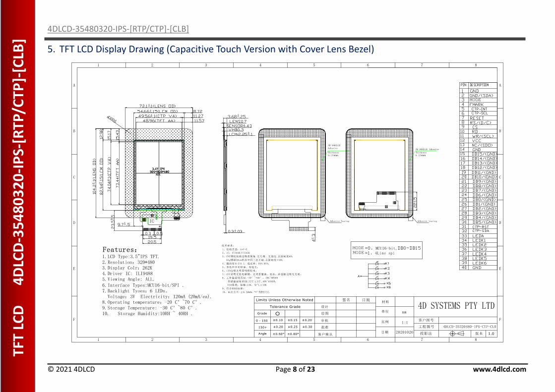
4DLCD-35480320-IPS is a colour active-matrix LCD module incorporating amorphous silicon IPS TFT (Thin Film Transistor). It is composed of a colour TFT-LCD panel, driver IC, FPC and a backlight unit and with/without a Resistive/Capacitive Touch Panel (RTP or CTP), and with/without Cover Lens Bezel (CLB). The module display area contains 320 x 480 pixels. This product accords with RoHS environmental criterion.
ITEM CONTENTS UNIT LCD Type TFT / Transmissive / IPS
Size 3.5 Inch
Viewing Direction ALL
Display Mode Normally Black
LCD (W × H × T)
4DLCD-35320480-IPS 54.66x 82.94 x 2.28
mm 4DLCD-35320480-IPS-RTP 54.66x 82.94 x 3.6
4DLCD-35320480-IPS-CTP 54.66 x 83.00 x 3.68
4DLCD-35320480-IPS-CTP-CLB 72.10 x 104.20 x.3.68 (Including CLB)
Active Area (W × H) 48.96 × 73.44 mm
Dot Pitch (W × H) 0.2025 × 0.2025 mm
Number of Dots (Pixels) 320 (RGB) × 480
Driver IC ILI9488
Backlight Type 6 LEDs
Surface Luminance
4DLCD-35320480-IPS 320 (typical)
cd/m2 4DLCD-35320480-IPS-RTP 270 (typical)
4DLCD-35320480-IPS-CTP 295 (typical)
4DLCD-35320480-IPS-CTP-CLB 295 (typical)
Interface Type MCU-16bit/SPI
Color Depth 262K
Pixel Arrangement RGB Vertical Stripe
Surface Treatment AG
Input Voltage 2.8 (typical) V
With/Without TP
4DLCD-35320480-IPS- Without TP 4DLCD-35320480-IPS-RTP – With Resistive Touch 4DLCD-35320480-IPS-CTP – With Capacitive Touch 4DLCD-35320480-IPS-CTP-CLB – Capacitive Touch CLB
Weight
4DLCD-35480320 19.4
g 4DLCD-35480320 - RTP 28.6
4DLCD-35480320 - CTP 38.0
4DLCD-35480320 -CTP-CLB 43.4

4DLCD-35480320-IPS-[RTP/CTP]-[CLB]
© 2021 4DLCD Page 4 of 23 www.4dlcd.com
TFT
LCD
4
DLC
D-3
54
80
32
0-I
PS-
[RTP
/CTP
]-[C
LB]
Note 1: RoHS compliant Note 2: LCD weight tolerance: ± 5%.
Part Number Details: 4DLCD 4D Systems LCD Display 35480320 3.5-inch, 320 x 480 Resolution RTP Resistive Touch CTP Capacitive Touch CLB Cover Lens Bezel

4DLCD-35480320-IPS-[RTP/CTP]-[CLB]
© 2021 4DLCD Page 5 of 23 www.4dlcd.com
TFT
LCD
4
DLC
D-3
54
80
32
0-[
RTP
/CTP
]-[C
LB] 2. TFT LCD Display Drawing (Non-Touch Version)

4DLCD-35480320-IPS-[RTP/CTP]-[CLB]
© 2021 4DLCD Page 6 of 23 www.4dlcd.com
TFT
LCD
4
DLC
D-3
54
80
32
0-I
PS-
[RTP
/CTP
]-[C
LB]
3. TFT LCD Display Drawing (Resistive Touch Version)

4DLCD-35480320-IPS-[RTP/CTP]-[CLB]
© 2021 4DLCD Page 7 of 23 www.4dlcd.com
TFT
LCD
4
DLC
D-3
54
80
32
0-I
PS-
[RTP
/CTP
]-[C
LB]
4. TFT LCD Display Drawing (Capacitive Touch Version)
4DLCD-35480320-IPS-[RTP/CTP]-[CLB]
© 2021 4DLCD Page 8 of 23 www.4dlcd.com
TFT
LCD
4
DLC
D-3
54
80
32
0-I
PS-
[RTP
/CTP
]-[C
LB]
5. TFT LCD Display Drawing (Capacitive Touch Version with Cover Lens Bezel)
4DLCD-35480320-IPS-[RTP/CTP]-[CLB]
© 2020 4DLCD Page 9 of 23 www.4dlcd.com
TFT
LCD
4
DLC
D-3
54
80
32
0-[
RTP
/CTP
]-[C
LB]
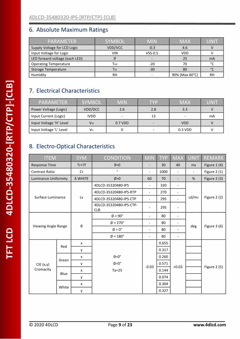
6. Absolute Maximum Ratings
PARAMETER SYMBOL MIN MAX UNIT Supply Voltage for LCD Logic VDD/VCC -0.3 4.6 V
Input Voltage for Logic VIN VSS-0.5 VDD V
LED forward voltage (each LED) IF - 25 mA
Operating Temperature TOP -20 70 °C
Storage Temperature TST -30 80 °C
Humidity RH - 90% (Max 60°C) RH
7. Electrical Characteristics
PARAMETER SYMBOL MIN TYP MAX UNIT Power Voltage (Logic) VDD/DCC 2.6 2.8 3.3 V
Input Current (Logic) IVDD - 13 - mA
Input Voltage ‘H’ Level VIH 0.7 VDD - VDD V
Input Voltage ‘L’ Level VIL 0 - 0.3 VDD V
8. Electro-Optical Characteristics
ITEM SYM CONDITION MIN TYP MAX UNIT REMARK Response Time Tr+Tf θ=0 - 30 40 ms Figure 1 (4)
Contrast Ratio Cr ° - 1000 - - Figure 2 (1)
Luminance Uniformity δ WHITE ∅=0 60 70 - % Figure 2 (3)
Surface Luminance Lv
4DLCD-35320480-IPS - 320 -
cd/m2 Figure 2 (2)
4DLCD-35320480-IPS-RTP - 270 -
4DLCD-35320480-IPS-CTP - 295 -
4DLCD-35320480-IPS-CTP-CLB
- 295 -
Viewing Angle Range θ
∅ = 90° - 80 -
deg Figure 3 (6) ∅ = 270° - 80 -
∅ = 0° - 80 -
∅ = 180° - 80 -
CIE (x,y) Cromacity
Red x
-0.03
0.655
+0.03
Figure 2 (5)
y 0.317
Green x θ=0° 0.260
y ∅=0° 0.571
Blue x Ta=25 0.144
y 0.074
White x 0.304
y 0.327

4DLCD-35480320-IPS-[RTP/CTP]-[CLB]
© 2021 4DLCD Page 10 of 23 www.4dlcd.com
TFT
LCD
4
DLC
D-3
54
80
32
0-I
PS-
[RTP
/CTP
]-[C
LB]
9. Backlight Characteristics
PARAMETER SYMBOL MIN TYP MAX UNIT Voltage for LED backlight (Each LED)
Vl - 3.2 3.4 V
Current for LED backlight (Each LED)
Il-each - 20 25 mA
Current for LED backlight (Total – 6 LEDS)
Il - 120 150 mA
LED Lifetime (50% of original brightness)
- 30000 - - Hrs
Note: The LED lifetime is defined as the module brightness decrease to 50% original brightness at Ta=25°C.
Note 1: Contrast Ratio (CR) is defined mathematically as below, for more information see Figure 1.
Contrast Ratio = Average Surface Luminance with all white pixels (P1, P2, P3, P4, P5)
Average Surface Luminance with all black pixels (P1, P2, P3, P4, P5)
Note 2: Surface luminance is the LCD surface from the surface with all pixels displaying white. For more information, see Figure 2.
Lv = Average Surface Luminance with all white pixels (P1, P2, P3, P4, P5)
Note 3: The uniformity in surface luminance δ WHITE is determined by measuring luminance at each test position 1 through 5, and then dividing the maximum luminance of 5 points luminance by minimum luminance of 5 points luminance. For more information, see Figure 2.
δ WHITE = Minimum Surface Luminance with all white pixels (P1, P2, P3, P4, P5)
Maximum Surface Luminance with all white pixels (P1, P2, P3, P4, P5)
Note 4: Response time is the time required for the display to transition from white to black (Rise Time, Tr) and from black to white (Decay Time, Tf). For additional information see FIG 1. The test equipment is Autronic-Melchers ConoScope series.
Note 5: CIE (x, y) chromaticity, the x, y value is determined by measuring luminance at each test position 1 through 5, and then make average value.
Note 6: Viewing angle is the angle at which the contrast ratio is greater than 2. For TFT module the contrast ratio is greater than 10. The angles are determined for the horizontal or x axis and the vertical or y axis with respect to the z axis which is normal to the LCD surface. For more information, see Figure3.
Note 7: For viewing angle and response time testing, the testing data is based on Autronic-Melchers ConoScope series. Instruments for Contrast Ratio, Surface Luminance, Luminance Uniformity, CIE the test data is based on TOPCONs BM-5 photo detector.

4DLCD-35480320-IPS-[RTP/CTP]-[CLB]
© 2021 4DLCD Page 11 of 23 www.4dlcd.com
TFT
LCD
4
DLC
D-3
54
80
32
0-I
PS-
[RTP
/CTP
]-[C
LB]
Figure 1. The definition of response time
Figure 2. Measuring method for Contrast ratio, surface luminance, Luminance uniformity, CIE (x, y) chromaticity
Figure 3. The definition of viewing angle

4DLCD-35480320-IPS-[RTP/CTP]-[CLB]
© 2021 4DLCD Page 12 of 23 www.4dlcd.com
TFT
LCD
4
DLC
D-3
54
80
32
0-I
PS-
[RTP
/CTP
]-[C
LB]
10. Interface Descriptions
10.1 LCD Interface
PIN NO. SYMBOL DESCRIPTION REMARK 1 GND Ground
2 GND/(SDI) Ground for MCU mode/ Serial Data Input signal for SPI mode
3 MODE MCU-16bit / SPI mode selection pin Note 1
4 FMARK Tearing effect output signal
5 YD/CTP_INT The touch panel Y bottom pin for RTP / Interrupt signal from CTP/No Connection (NC) for Non touch Version
Note 3
6 XL/CTP_SCL The touch panel X left pin for RTP/ I2C SCL for CTP / No Connection (NC) for Non touch Version
Note 3
7 RESET Reset input signal
8 RS/(D/C) Instruction Register/Data Register selection pin for MCU mode / Data or Command selection for SPI mode
9 CS Chip select input pin
10 RD/(VCC) Read signal for MCU mode / Tie to VCC for SPI mode
11 WR/(SCL) Write signal for MCU mode / SPI Serial Clock for SPI mode
12 VCC Power supply (Logic)
13 NC/(SDO) No Connect for MCU mode / Serial Data Output for SPI mode
14 GND Ground
15 DB15/(GND) Databus DB15 for MCU mode / Tie to GND for SPI mode Note 2
16 DB14/(GND) Databus DB14 for MCU mode / Tie to GND for SPI mode Note 2
17 DB13/(GND) Databus DB13 for MCU mode / Tie to GND for SPI mode Note 2
18 DB12/(GND) Databus DB12 for MCU mode / Tie to GND for SPI mode Note 2
19 DB11/(GND) Databus DB11 for MCU mode / Tie to GND for SPI mode Note 2
20 DB10/(GND) Databus DB10 for MCU mode / Tie to GND for SPI mode Note 2
21 DB9/(GND) Databus DB9 for MCU mode / Tie to GND for SPI mode Note 2
22 DB8/(GND) Databus DB8 for MCU mode / Tie to GND for SPI mode Note 2
23 DB7/(GND) Databus DB7 for MCU mode / Tie to GND for SPI mode Note 2
24 DB6/(GND) Databus DB6 for MCU mode / Tie to GND for SPI mode Note 2
25 DB0/(GND) Databus DB0 for MCU mode / Tie to GND for SPI mode Note 2
26 DB1/(GND) Databus DB1 for MCU mode / Tie to GND for SPI mode Note 2
27 DB2/(GND) Databus DB2 for MCU mode / Tie to GND for SPI mode Note 2
28 DB3/(GND) Databus DB3 for MCU mode / Tie to GND for SPI mode Note 2
29 DB4/(GND) Databus DB4 for MCU mode / Tie to GND for SPI mode Note 2
30 DB5/(GND) Databus DB5 for MCU mode / Tie to GND for SPI mode Note 2
31 YU/CTP_RST The touch panel Y up pin for RTP / Reset pin for CTP / No Connection (NC) for Non touch Version
Note 3
32 XR/CTP_SDA The touch panel X right pin for RTP / I2C SDA Pin for CTP / No Connection (NC) for Non touch Version
Note 3
33 LEDA Anode of LED Backlight
34 LEDK1 Cathode1 of LED Backlight
35 LEDK2 Cathode2 of LED Backlight
36 LEDK3 Cathode3 of LED Backlight
37 LEDK4 Cathode4 of LED Backlight
38 LEDK5 Cathode5 of LED Backlight
39 LEDK6 Cathode6 of LED Backlight
40 GND Ground

4DLCD-35480320-IPS-[RTP/CTP]-[CLB]
© 2021 4DLCD Page 13 of 23 www.4dlcd.com
TFT
LCD
4
DLC
D-3
54
80
32
0-I
PS-
[RTP
/CTP
]-[C
LB]
Note 1: Interface Mode Selection (pin 3)
Value Interface Remark 0 MCU 16bit Databus: DB0~DB15
1 SPI 4 wire SPI mode
Note 2: Pins 15 to 30 are grounded on SPI mode. Note 3: Pins 5,6,31 and 32 are only applicable to touch screen displays (4DLCD-xxxxxxxx-RTP/CTP).
Note the pinout of this 3.5” display differs from the pinout on 2.4”, 2.8” and 3.2” displays, for just the SPI Mode (Pin8 and Pin11), so if working with 2.4”, 2.8” and 3.2” displays in the 4DLCD family, take note that the MCU mode pinout is the same and backwards compatible, but SPI pinout is not identical.
10.2 CTP Interface The Capacitive Touch is driven by a Focaltech FT5446 capacitive touch driver IC, which utilizes an I2C interface, and is capable of 5-point touch.

4DLCD-35480320-IPS-[RTP/CTP]-[CLB]
© 2021 4DLCD Page 14 of 23 www.4dlcd.com
TFT
LCD
4
DLC
D-3
54
80
32
0-I
PS-
[RTP
/CTP
]-[C
LB]
11. Backlight Example Circuit
The backlight circuit can be easily driven off a 5V supply. The voltage needs to be higher than the forward voltage of the LED’s and other drops in the circuit, which can be found in section 9. A 3.3V supply typically does not meet this requirement, so a 5V supply is normally used.
In this circuit, a simple transistor is used to switch each of the LED’s on, where each LED is current limited through its own resistor. The transistor base can be PWM’ed if required (Label BACKLIGHT below), to give dimming control. An example PWM frequency that could be used is 3Khz, however it is up to the Designer to determine what is suitable for the application.
The resistance feeding each LED can be calculated using Ohms Law, V=I*R. We want to calculate R, so R=V/I Supply Voltage = 5V LED Forward Voltage = 3.2V (see section 9) Estimated voltage drop over transistor = 0.3V Target current per LED = 20mA to 25mA (use 22mA in this example) (See section 9) Formula is then R = (5V-3.2V-0.3V) / 0.022A = 68ohms for each LED (LEDK1 to LEDK6)

4DLCD-35480320-IPS-[RTP/CTP]-[CLB]
© 2021 4DLCD Page 15 of 23 www.4dlcd.com
TFT
LCD
4
DLC
D-3
54
80
32
0-I
PS-
[RTP
/CTP
]-[C
LB]
12. Initialisation Code
//*********Hardware reset*********// LCD_RESET=1; Delayms(15); LCD_RESET=0; Delayms(120); LCD_RESET=1; Delayms(120); //********Start Initial Sequence*******// WriteComm(0xE0); //P-Gamma WriteData(0x00); WriteData(0x13); WriteData(0x18); WriteData(0x04); WriteData(0x0F); WriteData(0x06); WriteData(0x3A); WriteData(0x56); WriteData(0x4D); WriteData(0x03); WriteData(0x0A); WriteData(0x06); WriteData(0x30); WriteData(0x3E); WriteData(0x0F); WriteComm(0XE1); //N-Gamma WriteData(0x00); WriteData(0x13); WriteData(0x18); WriteData(0x01); WriteData(0x11); WriteData(0x06); WriteData(0x38); WriteData(0x34); WriteData(0x4D); WriteData(0x06); WriteData(0x0D); WriteData(0x0B); WriteData(0x31); WriteData(0x37); WriteData(0x0F); WriteComm(0xC0); WriteData(0x18); WriteData(0x16); WriteComm(0xC1); WriteData(0x45); WriteComm(0xC5); //VCOM WriteData(0x00); WriteData(0x63); WriteData(0x01); WriteComm(0x36); WriteData(0x48);

4DLCD-35480320-IPS-[RTP/CTP]-[CLB]
© 2021 4DLCD Page 16 of 23 www.4dlcd.com
TFT
LCD
4
DLC
D-3
54
80
32
0-I
PS-
[RTP
/CTP
]-[C
LB]
WriteComm(0x3A); //Interface Mode Control WriteData(0x55); WriteComm(0xB0); //Interface Mode Control WriteData(0x00); WriteComm(0xB1); //Frame rate 70HZ WriteData(0xB0); WriteComm(0xB4); WriteData(0x02); WriteComm(0xB6); //RGB/MCU Interface Control WriteData(0x02); //WriteData(0x22); WriteComm(0xE9); WriteData(0x00); WriteComm(0xF7); WriteData(0xA9); WriteData(0x51); WriteData(0x2C); WriteData(0x82); WriteComm(0x11); WriteComm(0x21); Delay(120); WriteComm(0x29);

4DLCD-35480320-IPS-[RTP/CTP]-[CLB]
© 2021 4DLCD Page 17 of 23 www.4dlcd.com
TFT
LCD
4
DLC
D-3
54
80
32
0-I
PS-
[RTP
/CTP
]-[C
LB]
13. LCD Timing Details
13.1 Timing Chart
SIGNAL SYMBOL PARAMETER MIN MAX UNIT DESCRIPTION
DCX tast Address setup time 0 - ns -
taht Address hold time (Write/Read) 0 - ns -
CSX
tchw CSX “H” pulse width 0 - ns -
tcs Chip Select setup time 15 - ns
trcs Chip Select setup time (Read ID) 45 - ns
trcsfm Chip Select setup time (Read FM) 355 - ns
tcsf Chip Select Wait time (Write/Read) 10 - ns
WRX
twc Write cycle 66 - ns -
twrh Write Control Pulse H duration 15 - ns -
twrl Write Control Pulse L duration 15 - ns -
RDX(FM)
trcfm Read cycle (FM) 450 - ns
trdhfm Read Control Pulse H duration (FM) 90 - ns
trdlfm Read Control Pulse L duration (FM) 355 - ns
RDX(ID)
trc Read cycle (ID) 160 - ns
trdh Read Control Pulse H duration 90 - ns
trdl Read Control Pulse L duration 45 - ns
D[17:0]
tdst Write data setup time 10 - ns
tdht Write data hold time 10 - ns
trat Read access time - 40 ns
Tratfm Read access time - 340 ns
trod Read output disable time 20 80 ns
Timing parameter (VDD=3.3V, GND=0V, Ta=25C̊)

4DLCD-35480320-IPS-[RTP/CTP]-[CLB]
© 2021 4DLCD Page 18 of 23 www.4dlcd.com
TFT
LCD
4
DLC
D-3
54
80
32
0-I
PS-
[RTP
/CTP
]-[C
LB]
13.2 Reset Timing
SIGNAL SYMBOL PARAMETER MIN MAX UNIT
RESET
tRW Reset low pulse width 10 - us
tRT Reset complete time - 5 (note1) ms
- 120 (note2) ms
Note 1: When reset applied during SLPIN mode Note 2: When reset applied during SLPOUT mode.
13.3 Power On Sequence
13.3.1 Case 1 - RES line is held High or Unstable by Host at Power ON
4DLCD-35480320-IPS-[RTP/CTP]-[CLB]
© 2021 4DLCD Page 19 of 23 www.4dlcd.com
TFT
LCD
4
DLC
D-3
54
80
32
0-I
PS-
[RTP
/CTP
]-[C
LB]
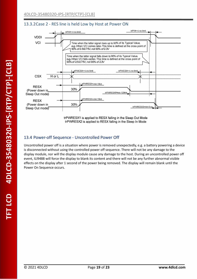
13.3.2 Case 2 - RES line is held Low by Host at Power ON
13.4 Power-off Sequence - Uncontrolled Power Off
Uncontrolled power off is a situation where power is removed unexpectedly, e.g. a battery powering a device is disconnected without using the controlled power off sequence. There will not be any damage to the display module, nor will the display module cause any damage to the host. During an uncontrolled power off event, ILI9488 will force the display to blank its content and there will not be any further abnormal visible effects on the display after 1 second of the power being removed. The display will remain blank until the Power On Sequence occurs.

4DLCD-35480320-IPS-[RTP/CTP]-[CLB]
© 2021 4DLCD Page 20 of 23 www.4dlcd.com
TFT
LCD
4
DLC
D-3
54
80
32
0-I
PS-
[RTP
/CTP
]-[C
LB]
14. Reliability Test
No. SYMBOL TEST CONDITION REMARK
1 High Temperature Storage
80℃±2℃ 96H
After test cosmetic and electrical defects should not
happen.
Restore 2H at 25℃
Power off
2 Low Temperature Storage
-30℃±2℃ 96H
Restore 2H at 25℃
Power off
3 High Temperature Operation 70℃±2℃ 96H
Power on
4 Low Temperature Operation -20℃±2℃ 96H
Power on
5 High Temperature & Humidity Operation
60℃±2℃
90%RH 96H
Power on
6 Temperature Cycle
-20℃←→25℃←→70℃
30min 5min 30min
After 10 cycles, restore 2H at 25℃
Power off
7 Vibration Test 10Hz~150Hz, 100m/s2, 120min
8 Shock Test Half-sinewave, 300m/s2, 11ms
Note: The Displays are of the highest rated ‘Grade A’, which allows for 0-4 defective pixels. A defective pixel could be solid Black (Dead), White, Red, Green or Blue.

4DLCD-35480320-IPS-[RTP/CTP]-[CLB]
© 2021 4DLCD Page 21 of 23 www.4dlcd.com
TFT
LCD
4
DLC
D-3
54
80
32
0-I
PS-
[RTP
/CTP
]-[C
LB]
15. Precautions for Using LCD Modules
15.1 Handing Precautions
• The display panel is made of glass and polarizer. The glass is fragile. It tends to be chipped during handling
especially on the edges. Please avoid dropping or jarring. Please be careful not subject it to a mechanical shock
by dropping it on impact.
• If the display panel is damaged and the liquid crystal substance leaks out, be sure not to get any of it in your
mouth. If the substance contacts your skin or clothes, wash it off using soap and water.
• Do not apply excessive force to the display surface or to the adjoining areas since this may cause the color tone
to vary. Do not touch the display with bare hands. This will stain the display area and degraded insulation
between terminals (some cosmetics are determined by the polarizer).
• The polarizer covering the display surface of the LCD module is soft and easily scratched. Handle this polarizer
carefully. Do not touch, push or rub the exposed polarizer with anything harder than an HB pencil lead
(e.g., glass, tweezers, etc.). Do not put or attach anything on the display area to avoid leaving marks on it.
Condensation on the surface and contact with terminals due to cold temperature will damage, stain or
contaminate the polarizer. After products are tested at low temperature they must be warmed up in a container
before coming into contact with room temperature air.
• If the display surface becomes contaminated, breathe on the surface and gently wipe it with a soft dry cloth. If
it is heavily contaminated, moisten the cloth with one of the following solvents
o Isopropyl alcohol
o Ethyl alcohol
Do not scrub hard as it might damage the display surface.
• Solvents other than those mentioned above may damage the polarizer. Especially the following.
o Water
o Ketone
o Aromatic solvents
Wipe off saliva or water drops immediately, contact with water over a long period of time may cause
deformation or color fading. Avoid contact with oil and fat.
• Take necessary precautions to minimize corrosion of the electrode. Corrosion of the electrodes is accelerated
by water droplets, moisture condensation or current flow in a high-humidity environment.
• Install the LCD Module by using the mounting holes. When mounting the LCD module, make sure it is free of
twisting, warping and distortion. In particular, do not forcibly pull or bend the I/O cable or the backlight cable.
• Do not attempt to disassemble or process the LCD module.
• NC terminal should be open. Do not connect anything on it.
• If the logic circuit power is off, do not apply input signals.
• Control Electro-Static Discharge. Since this module uses a CMOS LSI, the same careful attention should be paid
to electrostatic discharge as for an ordinary CMOS IC. To prevent destruction of the elements by static electricity,
ensure that an optimum work environment is maintained.

4DLCD-35480320-IPS-[RTP/CTP]-[CLB]
© 2021 4DLCD Page 22 of 23 www.4dlcd.com
TFT
LCD
4
DLC
D-3
54
80
32
0-I
PS-
[RTP
/CTP
]-[C
LB]
o Before removing the LCM from its packing case or incorporating it into a set, be sure that the module
and your body has the same electric potential. Be sure to ground your body when handling the LCD
modules.
o To reduce the amount of static electricity generated, do not conduct assembly and other work under
dry conditions. To reduce the generation of static electricity, please ensure that the air in the work
environment is not too dry. A relative humidity of 50%-60% is recommended. As much as possible,
make the electric potential of your work clothes and that of the work bench the ground potential.
o The LCD module is coated with a film to protect the display surface. Be careful when peeling off this
protective film since static electricity may be generated.
• Since the LCM has been assembled and adjusted with a high degree of precision, avoid applying excessive shocks
to the module or making any alterations or modifications to it.
o Do not alter, modify or change the shape of the tab on the metal frame.
o Do not make extra holes on the printed circuit board, modify its shape or change the positions of
components to be attached.
o Do not damage or modify the pattern writing on the printed circuit board.
o Absolutely do not modify the zebra rubber strip (conductive rubber) or heat seal connector.
o Do not drop, bend or twist the LCM.
15.2 Storage Precautions
When storing the LCD modules, the following precautions are necessary.
• Store them in a sealed polyethylene bag. If properly sealed, there is no need for the desiccant.
• Store them in a dark place. Do not expose to sunlight or fluorescent light, keep the temperature between 0℃
and 35℃, and keep the relative humidity between 40%RH and 60%RH.
• The polarizer surface should not come in contact with any other objects. (We advise you to store them in an
anti-static electricity container in which they were shipped. Some Liquid crystals solidify under low temperature
(below the storage temperature range) leading to defective orientation or the generation of air bubbles (black
or white). Air bubbles may also be generated if the module is subjected to low temperature.
• If the LCD modules have been operating for a long time showing the same display patterns, the display patterns
may remain on the screen as ghost images and a slight contrast irregularity may also appear. A normal operating
status can be regained by suspending use for some time. It should be noted that this phenomenon does not
adversely affect performance reliability.
• To minimize the performance degradation of the LCD modules resulting from destruction caused by static
electricity etc., please avoid holding the following sections when handling the modules’
o Exposed area of the printed circuit board
o Terminal electrode sections
4DLCD-35480320-IPS-[RTP/CTP]-[CLB]
© 2021 4DLCD Page 23 of 23 www.4dlcd.com
TFT
LCD
4
DLC
D-3
54
80
32
0-I
PS-
[RTP
/CTP
]-[C
LB]
16. Legal Information
Proprietary Information The information contained in this document is the property of 4D LCD Pty. Ltd.; these may be the subject of patents pending or granted, and must not be copied or disclosed without prior written permission. 4D LCD endeavors to ensure that the information in this document is correct and fairly stated but does not accept liability for any error or omission. The development of 4D LCD products and services is continuous and published information may not be up to date. It is important to check the current position with 4D LCD. 4D LCD reserves the right to modify, update or makes changes to Specifications or written material without prior notice at any time. All trademarks belong to their respective owners and are recognized and acknowledged. Disclaimer of Warranties & Limitation of Liability 4D LCD Pty Ltd makes no warranty, either expressed or implied with respect to any product, and specifically disclaims all other warranties, including but without limitation to; warranties for merchantability, non-infringement and fitness for any particular purpose. Information contained in this publication regarding device applications and the like is provided only for your convenience and may be superseded by updates. It is your responsibility to ensure that your application meets with your specifications. Images and graphics used throughout this document are for illustrative purposes only. All images and graphics used are possible to be displayed on the 4D LCD range of products, however the quality may vary. In no event shall 4D LCD be liable to the buyer or to any third party for any indirect, incidental, special, consequential, punitive or exemplary damages (including but without limitation to; lost profits, lost savings, or loss of business opportunity) arising out of or relating to any product or service provided or to be provided by 4D LCD, or the use or inability to use the same, even if 4D LCD has been advised of the possibility of such damages. 4D LCD products are not fault tolerant nor designed, manufactured or intended for use or resale as on line control equipment in hazardous environments requiring fail – safe performance, such as in the operation of nuclear facilities, aircraft navigation or communication systems, air traffic control, direct life support machines or weapons systems in which the failure of the product could lead directly to death, personal injury or severe physical or environmental damage (‘High Risk Activities’). 4D LCD and its suppliers specifically disclaim any expressed or implied warranty of fitness for High Risk Activities. Use of 4D LCD products and devices in 'High Risk Activities' and in any other application is entirely at the buyer’s risk, and the buyer agrees to defend, indemnify and hold harmless 4D LCD from any and all damages, claims, suits, or expenses resulting from such use. No licenses are conveyed, implicitly or otherwise, under any 4D LCD intellectual property rights.


![Proxima Systems - IProx BMS - Datasheet [en]](https://img.pdfslide.us/doc/110x75/55c72640bb61eb064d8b4681/proxima-systems-iprox-bms-datasheet-en.jpg)