Embed Size (px)
Citation preview

i
JAN LIPPONEN
DATA TRANSFER OPTIMIZATION IN FPGA BASED EMBEDDED
LINUX SYSTEM
Master of Science Thesis
Examiner: D.Sc. Timo D. Hämäläinen Examiners and topic approved by the Dean of the Faculty of Computing and Electrical Engineering on 30th November 2017

ABSTRACT
JAN LIPPONEN: Data transfer optimization in FPGA based embedded Linux system Tampere University of technology Master of Science Thesis, 69 pages, 10 Appendix pages May 2018 Master’s Degree Programme in Electrical Engineering Major: Embedded Systems Examiner: D.Sc. Timo D. Hämäläinen Keywords: SoC, embedded Linux, FPGA, DMA, data transfer
The main goal of this thesis was to optimize the efficiency of data transfer in an FPGA
based embedded Linux system. The target system is a part of a radio transceiver appli-
cation receiving high data rates to an FPGA chip, from where the data is made accessi-
ble to a user program using a DMA operation utilizing Linux kernel module. The initial
solution, however, used excessive amounts of CPU time to make the kernel module
buffered data accessible by the user program. Further optimization of the data transfer
was required by upcoming phases of the project.
Two data transfer optimization methods were considered. The first solution would use
an architecture enabling the FPGA originating data to be accessed directly from the user
program via a data buffer shared with the kernel. The second solution utilized a DMAC
(DMA controller) hardware component capable of moving the data from the kernel
buffer to the user program. The second choice was later rejected due to high platform
dependency on such an implementation.
A working solution, for the shared buffer optimization method, was found by going
through Linux memory management related literature. The implemented solution uses
the mmap system call function to remap a kernel module allocated data buffer for user
program access. To compare the performance of the implemented solution to the initial
one, a data transfer test system was implemented. This system enables pre-defined data
to be generated in the FPGA with varying data rates. It was shown in the performed
tests that the maximum throughput was increased by ~25% (from ~100 MB/s to ~125
MB/s) using the optimized solution. No exact maximum data rates were discovered be-
cause of a test data generation related constraint.
The increase in throughput is considered as a significant result for the radio transceiver
application. The implemented optimization solution is also expected to be easily porta-
ble to any Linux system.

TIIVISTELMÄ
JAN LIPPONEN: Datasiirron optimointi FPGA mikropiiriin pohjautuvassa sulautetussa Linux-järjestelmässä Tampereen teknillinen yliopisto Diplomityö, 69 sivua, 10 liitesivua Toukokuu 2018 Sähkötekniikan diplomi-insinöörin tutkinto-ohjelma Pääaine: Sulautetut järjestelmät Tarkastaja: D.Sc. Timo D. Hämäläinen Avainsanat: SoC, sulautettu Linux, FPGA, DMA, datasiirto
Tämän diplomityön tavoitteena oli optimoida datasiirron tehokkuus FPGA-mikropiiriin
perustuvassa sulautetussa Linux-järjestelmässä. Työn kohdejärjestelmä on osa
radiovastaanotin -sovellusta, joka vastaanottaa suuria määriä dataa FPGA- mikropiirille.
FPGA:lta data tehdään käyttäjäohjelman hyödynnettäväksi käyttäen oikosiirtoa (DMA)
hyödyntävää Linux-ytimen laiteohjainta. Alkuperäinen toteutus käytti kuitenkin suuren
määrän suoritinaikaa tämän datan viemiseen laiteohjaimelta käyttäjäohjelmalle ja
projektin tulevat vaiheet vaativat datasiirron optimointia.
Työssä päätettiin tutkia kahta eri optimimointimenetelmää. Ensimmäinen ratkaisu
käyttäisi arkkitehtuuria, joka mahdollistaisi FPGA:lta lähtöisin olevan datan käytön
suoraan käyttäjäohjelmassa Linux-ytimen kanssa jaetun datapuskurin kautta. Toinen
ratkaisusuunnitelma hyödynsi DMAC (oikosiirto-ohjain) komponenttia, joka kykenee
toteuttamaan datan siirron laiteohjaimelta käyttäjäohjelmalle. Tämä ratkaisumalli
kuitenkin myöhemmin hylättiin sen aiheuttaman laitteistoriippuvuuden takia.
Toimiva ratkaisumalli jaetulle datapuskurille löytyi käymällä läpi Linuxin
muistinhallintaa käsittelevää kirjallisuutta. Toteutettu ratkaisu hyödynsi mmap
systeemikutsua Linuxin ytimessä varatun muistipuskurin muokkaamiseksi
käyttäjäohjelmasta hyödynnettäväksi. Toteutetun ja alkuperäisen ratkaisun
suorituskykyjen vertaamista varten toteutettiin datasiirto-testijärjestelmä. Tämä
järjestelmä mahdollistaa ennalta määritetyn datan tuottamisen FPGA:lla vaihtelevilla
siirtonopeuksilla.
Toteutetuissa testeissä todennettiin, että järjestelmän maksimaalinen tiedonsiirtonopeus
kasvoi noin 25 prosenttia (~100 megatavusta sekunnissa ~125 megatavuun sekunnissa)
käyttäen optimimoitua ratkaisua. Tarkkoja maksimaalisia tiedonsiirtonopeuksia ei
pystytty todentamaan testidatan tuottamiseen liittyvän rajoituksen takia.
25 prosentin lisäys maksimaaliseen tiedonsiirtonopeuteen nähtiin kohdejärjestelmän
kannalta merkittävänä tuloksena. Toteutetun optimimointiratkaisun odotetaan myös
olevan helposti vietävissä mihin tahansa Linux-järjestelmään.

PREFACE
In spring 2017, I received an email seeking for embedded developers to work in a project
described as an "engineer’s dream" by our embedded segment manager. Little did I knew
what would come when I clicked the “reply” button. I am grateful that I was given the
opportunity by Wapice Ltd to be part of this project and to learn from the best. At the
time, Xilinx technologies, the Yocto Project and Linux kernel module development were
new things to me, but under the guidance of Jouko Haapaluoma I gained high-level
knowledge on all these areas.
This thesis is highly grounded on the knowledge gained from the "engineer’s dream” and
I want to express my gratitude to all parties involved in the project that has taken me from
the depths of the Linux kernel to shores of Hailuoto – both being places I have never been
in before. This project has given me the courage to call myself an embedded software
developer.
Tampere, 22.5.2018
Jan Lipponen
CONTENTS
1. INTRODUCTION ................................................................................................ 1
2. LINUX ON EMBEDDED SYSTEMS .................................................................. 3
2.1 Embedded system features .......................................................................... 3
2.2 Choosing between OS and no-OS ............................................................... 5
2.3 Linux features ............................................................................................. 7
2.4 Linux hardware abstraction ......................................................................... 8
2.4.1 Address spaces .............................................................................. 9
2.4.2 Process/kernel model .................................................................. 10
3. LINUX DEVICE DRIVERS ............................................................................... 13
3.1 Modules .................................................................................................... 13
3.2 Device and driver types ............................................................................ 14
3.3 Interrupt handling ..................................................................................... 15
3.4 Memory allocation .................................................................................... 16
3.4.1 Slab layer .................................................................................... 17
3.4.2 kmalloc() .................................................................................... 19
3.4.3 vmalloc() .................................................................................... 20
3.4.4 ioremap() .................................................................................... 21
3.5 Direct memory access ............................................................................... 21
3.5.1 DMA Mapping............................................................................ 22
4. FPGA BASED SOC-PLATFORM ...................................................................... 24
4.1 Field programmable gate arrays ................................................................ 25
4.1.1 FPGA comparison to other ICs.................................................... 25
4.1.2 General FPGA architecture ......................................................... 26
4.1.3 FPGA clocking ........................................................................... 30
4.1.4 FPGA programming .................................................................... 30
4.2 Xilinx Zynq-7000 devices ......................................................................... 31
4.2.1 PS-PL interfacing ........................................................................ 33
4.3 FPGA based DMA transfer ....................................................................... 34
5. DATA TRANSFER OPTIMIZATION ................................................................ 36
5.1 Test system components ........................................................................... 36
5.1.1 Sample generator ........................................................................ 38
AXI4-Stream interface .............................................................................. 40
5.1.2 Vivado design with AXI DMA core ............................................ 44
5.1.3 AXI DMA cyclic module ............................................................ 47
5.1.4 DMA test program ...................................................................... 51
5.2 Sequence diagram and analysis ................................................................. 54
5.2.1 Performance ................................................................................ 55
5.3 Data transfer optimization methods ........................................................... 55
5.3.1 Coherent DMA buffer ................................................................. 56
5.3.2 mmap implementation ................................................................. 58

6. EXPERIMENTS AND ANALYSIS .................................................................... 63
6.1 TLAST positioning test............................................................................. 64
6.2 Performance test ....................................................................................... 66
7. CONCLUSIONS ................................................................................................. 68
8. BIBLIOGRAPHY ............................................................................................... 70
APPENDIX A: The sample clock generator module
APPENDIX B: The counter data generator module
APPENDIX C: The sample generator module
APPENDIX D: AXI DMA platform device probe function
APPENDIX E: AXI DMA callback and read functions

LIST OF FIGURES
Figure 1. A generic embedded system structure, adapted from [1, p. 12]. .............. 4
Figure 2. High-level overview of the Linux system structure, adapted from [7,
p. 6]. ...................................................................................................... 9
Figure 3. Application program-process relation, context switches and a
hardware interrupt. .............................................................................. 11
Figure 4. The slab allocator interfacing the slab layer subsystem, adapted
from [10, p. 247]. ................................................................................. 18
Figure 5. The general purpose caches of an ARM based Linux system. ................ 19
Figure 6. Functional block diagram of a typical SoC circuit, adapted from
[13, p. 4]. ............................................................................................. 24
Figure 7. General FPGA structure, adapted from [16, p. 3]. ............................... 27
Figure 8. A simplified LC element, adapted from [14, p. 74]................................ 28
Figure 9. A Boolean function represented by graphical logic gates. .................... 28
Figure 10. The implemented DMA test system on a Z-7010 based MicroZed
board. .................................................................................................. 37
Figure 11. The sample generator submodules as graphical blocks. ........................ 39
Figure 12. An AXI4-Stream wave diagram with 5 signals and counter data
payload, adapted from [24, p. 86]. ....................................................... 41
Figure 13. The sample generator test bench simulation showing the AXI4-
Stream protocol circuit output. ............................................................. 43
Figure 14. Clock division wave diagram. ............................................................... 44
Figure 15. The DMA test system as Vivado block design. ...................................... 46
Figure 16. The Vivado’s address editor tab associated with the test system. .......... 47
Figure 17. Illustration of a DMA ring buffer with concurrent writer and a
reader. ................................................................................................. 50
Figure 18. The DMA test system control sequence diagram. .................................. 54
Figure 19. The discussed data transfer optimization methods. ............................... 56
Figure 20. The TLAST positioning test results using 22.222 MB/s data rate. ......... 65
Figure 21. The performance test results. ................................................................ 66

LIST OF ABBREVIATIONS
ACP Accelerator coherency port
AMBA Advanced microcontroller bus architecture
API Application programming interface
ASIC Application-specific integrated circuit
ASSP Application-specific standard part
AXI Advanced eXtensible interface
AXI_GP AXI general purpose interface
AXI_HP High-performance AXI port
BRAM Block random-access memory
CLB Configurable logic blocks
CPLD Complex programmable logic device
CPU Central processing unit
DLL Digital delay-locked loop
DMA Direct memory access
DMAC Direct memory access controller
DRAM Dynamic random-access memory
DSP Digital signal processor / digital signal processing
EEPROM Electrically erasable programmable read-only memory
FIFO First in, first out
FPGA Field programmable gate array
GB Gigabyte (109 bytes)
GiB Gibibyte (230 bytes)
GP General purpose
GPIO General purpose input/output
GPL GNU general public license
HDL Hardware description language
HP High-performance
I/O Input/output
IC Integrated circuit
IOCTL Input/output control
IOMMU Input/output memory management unit
IoT Internet of things
IP Intellectual property
IRQ Interrupt request
ISA Industry standard architecture
ISR Interrupt service routine
LC Logic cell
LE Logic element
LUT Lookup table
MAC Multiply and accumulate
MIPS Millions of instructions per second
MM2S Memory-mapped to stream
mW Milliwatt
OCM On chip memory
OS Operating system
PC Personal computer
PCI Peripheral component interconnect

PL Programmable logic
PLD Programmable logic device
PLL Phase-locked loop
PS Processing system
RAM Random-access memory
ROM Read-only memory
S2MM Stream to memory-mapped
SCSI Small computer system interface
SoC System on a chip
SPARC Scalable processor architecture
SRAM Static random-access memory
TCP Transmission control protocol
UDP User datagram protocol
USB Universal serial bus
VHDL VHSIC hardware description language

1
1. INTRODUCTION
Embedded systems are everywhere and as technology advances devices powerful enough
running a full operating system, such as Linux, become available to low cost applications.
One of the biggest motivations in using an OS (operating system) in embedded applica-
tions is their networking capabilities. Embedded systems often interact with other systems
through networking interfaces, or through internet, but implementing a hardware depend-
ent bare metal networking software is often undesirable. Linux is a well-supported open
source operating system kernel distributed under GNU General Public License version 2,
making it an adjacent choice to many embedded applications.
Linux based systems are usually built respecting the kernel space / user space division;
the kernel space software entities interacting with system hardware, the device drivers,
are separated from user space applications. Eventually, this creates a need for transferring
data from kernel space to user space. A system using a camera module could work in this
manner; if a user application should request a picture frame from a camera peripheral, it
cannot interface the camera peripheral directly, but sends a request for the kernel. The
kernel then takes care of the transaction with the camera module via a device driver, after
which the frame is transferred to the requesting user application.
Applications performing high amounts of data transfer between the kernel space and the
user space can produce high stress on the system processor, thus limiting the achievable
data rate to/from a user application. This was the scenario in a customer project at Wapice
Ltd. The customer’s radio transceiver application was producing high amounts of data
from an FPGA chip to a kernel space allocated buffer using a FPGA implemented DMA
controller. It was initially known, that transferring this data from the kernel space allo-
cated buffer to a user space application was the bottleneck of the system and optimizing
this step was the goal of this thesis.
Two kernel space to user space data transfer optimization possibilities were initially de-
cided to be implemented; one with a shared data buffer enabling the FPGA originating
data to be accessed straight from a user space application, and one using a DMAC hard-
ware component capable of this data transfer on behalf of the system processor. The latter
was later rejected because of high platform dependency of such an implementation.
To implement such advanced data transfer scheme, comprehensive studies on Linux ker-
nel related topics was carried out. In Chapters 1-3 the reader is introduced to embedded
Linux systems and the essential parts of memory management and DMA operation theory

2
are presented to create grounds for an optimization implementation. In Chapter 4 the
FPGA technology is discussed and the reader is familiarized with the target device archi-
tecture. A data transfer test system is then constructed in Chapter 5 and a data transfer
optimization implementation is introduced. An optimization method is then tested and the
results are analyzed in Chapter 6. Finally, the Chapter 7 concludes the thesis.

3
2. LINUX ON EMBEDDED SYSTEMS
An embedded system can be defined as a combination of system hardware, software and
additional mechanical or electronic components designed to fulfill a predefined task. Cou-
ple of examples of such systems are an electric toothbrush and a microwave oven. These
devices are widely used in society by millions of users, but few come to think that there
is a CPU running software behind their operation. A contrast to an embedded system is a
PC (personal computer), also known as general-purpose computer, which does not have
any predefined task and the final operation of the machine is up to the end user of each
device. [1, p. 9]
Very often an embedded system is part of a larger system; one embedded system might
be in charge of controlling the brakes of a modern car while another displays the fuel
level on the dashboard and third controls the electronic fuel injection. Subsystems within
a larger system may – or may not – be aware of each other. In the given example one can
easily reason that the fuel injection should be cut off when a driver hits the breaks but this
should not affect the fuel level display. [1, p. 9]
Typically, when talking about computer systems, one tends to think about PCs and widely
used PC operating systems (OS) such as Windows and macOS, the market leaders of
desktop operating systems, but an embedded system may lack of OS entirely because of
low hardware capabilities [2]. Many embedded applications do not need an OS to fulfill
their purpose; software needed to operate an electric toothbrush may be simple enough to
run without OS services like task scheduling, memory management or hardware abstrac-
tion. This situation can, however, change if the toothbrush needs provide networking ca-
pabilities, like some wireless communication interface.
This chapter introduces the reader to some general features found in embedded systems,
introduces the motivation in the use of a well-known operating system and finally takes
a brief look into Linux kernel architecture aspects important for the rest of the thesis.
2.1 Embedded system features
All embedded systems including software also contain a processor, ROM (read-only
memory), where the executable code is stored, and RAM (random-access memory) for
runtime data manipulation by the processor. One or both of these memory types may be
external memory chips depending on the systems memory demands. An embedded sys-
tem also contains some sort of I/O (input/output), like pushbuttons (input) leading to de-
sired function of a MP3 player and sound coming out of the headphones (output). [1]

4
The input of a system could also be a sensor, a touch screen or a data link from another
system – or combination of any of these. The system output usually goes to a display or
to another system via a data link or the output makes changes to the physical world. So
far, we can illustrate a generic embedded system with a block diagram seen in the Figure
1. [1, p. 12]
Figure 1. A generic embedded system structure, adapted from [1, p. 12].
The block diagram seen in Figure 1 is also eligible to describe the working of a PC, but
it should be emphasized that embedded systems are designed to function with some spe-
cific kind of I/O to perform some predefined task, in contrast to PC’s virtually unlimited
use cases with alternating amount of I/O peripheral devices. Every unique embedded sys-
tem must meet different kind of design constraints and especially commercial products
have trade-offs between production cost and other desirable attributes like processing
power and memory capacity [1, p. 14]. The production cost can be one of many design
requirements an embedded system must meet.
Common embedded system design features with requirements include [1, pp. 14-15]:
1. Processing power
The maximum workload that the main chip needs to handle. One way to meas-
ure the processing power of a processor is the MIPS (millions of instructions per
second) rating. Another important feature is the processor’s word length that can
range from 4 to 64 bits. Many embedded systems are built with cheaper 4-, 8-
and 16-bit word length processors.
2. Memory capacity
The amount of memory needed to hold the executable software and the data
5
used to produce the output data. The output data may not be continuously ex-
ported from the system, but can also be written to a long term memory for later
export.
3. Number of units
The amount of units expected to be produced. This affects the production cost
and development cost trade-off. It may not be cost-effective to develop custom
hardware for a low-volume product, for example.
4. Power consumption
The amount of power the device needs for its operation. This is especially im-
portant for battery powered devices. Power consumption can also affect device
features like heat production, device weight, size and mechanical design.
5. Development cost
The cost of hardware and software engineering.
6. Production cost
The cost of system hardware production.
7. Lifetime
The required time for a device to stay operational.
8. Reliability
The operational reliability of a system. For example, it is not necessarily unac-
ceptable for your toothbrush to have a minor malfunction every now and then,
but your car’s brakes ought to be working 100 percent of the time.
In addition to these common requirements an embedded system faces functional require-
ments that gives the system its unique identity. [1, p. 16] After all the common and func-
tional requirements of a system have been specified, a system designer needs to architect
the implementation. One important design choice is between including an operating sys-
tem or not.
2.2 Choosing between OS and no-OS
It is common for system designers to initially think that a design solution without an op-
erating system, often called as a “no-OS” or as a “bare metal” system, is lighter, and
thereby faster, and more robust than a system with an OS [3]. Functionality of the first
operating systems was just to virtualize the system hardware with a collection of hardware
controlling routines. This enabled easier development of software and still today every
functionality of any system is possible to be implemented with a bare-metal application

6
[1]. Therefore, it is simple to conclude that an operating system produces unnecessary
memory footprint and that it cannot introduce as high performance as a bare metal solu-
tion would. However, it was showed in white paper (WP-01245-1.0) by Altera Corpora-
tion that with modern technologies this is not necessarily the case [3].
High performance and low jitter are especially important qualities in real-time systems1
where failure to meet a jitter deadline can result in severe outcomes like injury or death.
In 2014, Altera Corporation published a white paper comparing real-time performance
between a hand-optimized bare-metal and a high-level operating system solutions using
Cyclone V SoC (system on a chip) including an ARM Cortex-A9 processor. It was
showed in the white paper that, given the complexities of a modern multi-core application
processor, the bare-metal solution did not introduce any performance advantage com-
pared to the OS based solution. It was also noticed that it is remarkably difficult to create
optimized bare-metal solution, for such a modern processor, without the use of a modern
OS. [3]
In the terms of performance, most operating systems are developed to take full advantage
of multiple different processor architectures and it saves time not be obligated to rede-
velop optimized bare-metal solutions [3]. One of these OS provided processor architec-
ture depended services is called scheduling. Scheduling enables execution of multiple
programs seemingly in parallel even with a unicore processor [1]. With a unicore proces-
sor the programs are actually executed in turns scheduled by the operating system sched-
uling algorithm.
A bare-metal solution may still be a good choice for simple enough applications but as
the complexity grows beyond that of a LED blinker or an electric toothbrush the OS based
solution is usually a better choice [1]. Well known operating systems offer wide software
support for variety of different devices and, in the best case scenario, the hardware of the
used platform may already be fully abstracted by the OS offered device drivers. By using
a proven OS the system designer may concentrate on system-level optimization [3].
When choosing between a bare-metal solution and an OS based solution, the system de-
signer should consider all the system related constraints from hardware requirements to
application complexities. Another important service offered by many operating systems
is the networking stack, needed for communications between computer systems, and is
often not desirable to be implemented from scratch [1]. One operating system with such
capability is Linux. The Linux OS supports in addition to traditional internet protocols,
such as TCP (transmission control protocol) and UDP (user datagram protocol), many
other interconnection options enabling communications between all conceivable comput-
ers and operating systems [4, p. 733]. This is one of the reasons Linux is found in millions
1 Systems that have to respond to an external input within a finite and specified time period [6, p. 12].
Further real-time system characteristics are out of scope of this thesis.

7
of devices working in wide range of different tasks from wristwatches to mainframe com-
puters [4, p. 1].
2.3 Linux features
Linux is a member of Unix-like operating systems and it was originally developed by
Linus Torvalds in 1991 for IBM-compatible personal computers with Intel 80386 micro-
processors. Over the years hundreds of developers have worked with Linux in order to
make it available on multiple processor architectures such as Hewlett-Packard’s Alpha,
Intel’s Itanium, AMD’s AMD64, PowerPC and IBM’s zSeries. One of major benefits of
Linux is that its source code is distributed under GNU General Public License (GPL) and
is open to everyone. Linux includes the features of modern Unix OS such as a virtual file
system and virtual memory, lightweight processes, Unix signaling, support for symmetric
multiprocessor systems, and so on. [5, pp. 1-2]
The Linux kernel has multiple favors in comparison to many of its commercial competi-
tors [5, pp. 4-5]:
• Linux is cost-free
It is possible to install the whole system just with the cost of hardware.
• Linux is fully customizable
Compilation options enable customization of the kernel by choosing just needed fea-
tures. Furthermore, thanks to GPL, the kernel source code itself can be modified.
• Linux runs on inexpensive, low-end hardware platforms
It is possible to implement a network server with a system based in the Intel 80386
with only 4 MB of RAM.
• Linux is powerful
Linux has been developed to be highly efficient and many design choices have been
rejected because of their negative impact on performance.
• Linux is stable
Linux systems have a very low failure rate and maintenance time.
• Linux kernel can be very small and compact
The Linux kernel and some system programs used in this thesis only need 9.76 MB
of memory without any particular image size optimization.
• Linux is highly compatible with other operating systems

8
Linux is able to mount filesystems, for example, from Microsoft Windows, Mac OS
X, Solaris and SunOS. Linux supports multiple network layers and using suitable
libraries it can run some programs originally not written for Linux.
• Linux is well supported
Linux community serves back questions usually within hours after sending them to
newsgroups / mailing lists and new hardware drivers are often made available within
couple of weeks after new hardware products are introduced to the market.
An operating system build on top of the Linux kernel is called a Linux distribution and
all the distributions have their strengths and weaknesses in the target hardware and appli-
cation. Different distributions include different kind of a set of system software depending
on the target platform and the user preference. AsteriskNOW, for example, is a function-
ally specialized distribution developed to enable the user to easily create a voicemail or a
FAX server. The best known general desktop distributions, like Ubuntu and Debian, are
not well suited for embedded systems and it is more typical to use a platform specialized
distribution, or to build a custom one. [6, pp. 923-925]
2.4 Linux hardware abstraction
In some operating systems it is allowed for the user software to directly access the system
hardware but in Unix-like operating systems, such as Linux, this is restricted and the OS
hides the physical components from the user. When a user application needs to access a
hardware resource it requests this from the operating system and if the request is granted
by the OS kernel, it interacts with the hardware on behalf of the application. A request
for the kernel is called a system call. [5, pp. 8, 11] This basic structure of a Linux system
can be illustrated with Figure 2. To understand the role of a system call we first need to
take a look into how Linux handles memory address spaces and how programs are run in
a Linux system.

9
Figure 2. High-level overview of the Linux system structure, adapted from [7, p. 6].
2.4.1 Address spaces
The word length of a CPU determines the maximum of manageable address space. For
example, with a word length of 32-bits there is 232 bytes = 4 GiB (Gibibyte) of manage-
able memory. The conventional units, such as GB (Gigabyte) = 109 bytes, are not usable
for precise description because they are concluded from decimal powers [4, p. 7]. How-
ever, the conventional units are used throughout this thesis for better readability and be-
cause it is a custom to use the conventional units when measuring data transfer speed with
bit rate, defined in ISO/IEC 2382:2015 standard as bits per second [7].
The address space is not actually related to the amount of physical RAM used in the
system and therefore it is known as the virtual address space. In Linux, the virtual address
space is divided in the user space and in the kernel space with an architecture dependent
ratio so that the user space extends from 0 to TASK_SIZE – an architecture specific con-
stant. In 64-bit machines this may be more complicated because it is common to use less
than 64 bits for addressing to actually manage their enormous potential virtual address
space. The amount of address space will still be more than the amount of physical RAM.
Both the physical memory and the virtual address space are divided in equal size portions
called pages. The physical pages are usually referred to as page frames so that the word
page is reserved to describe the virtual memory pages. [4, pp. 8, 10, 11]
The kernel and CPU handles the relation between virtual address space and physical
memory by allocating virtual addresses to physical addresses via page tables. The virtual

10
memory pages are said to be mapped to physical page frames and this addressing infor-
mation is then stored to the page tables. The simplest implementation for a page table
structure would be an array with entries for each page pointing to an associated page
frame. Page tables are actually more complicated but further architecture behind the page
tables is out of scope of this thesis. [4, pp. 8, 10, 11]
Although a Linux system uses the same RAM for storing the kernel code (managing the
system hardware) and for the user applications, it is possible to restrict the user applica-
tions from performing hardware access with a simple rule: code that is stored in user space
is never allowed to read or to manipulate data stored in kernel space. The user space
applications still need to be able to somehow use hardware recourses. All modern proces-
sors introduce different kind of privilege levels for code execution and this is exploited
in the process/kernel model. [9, p. 8]
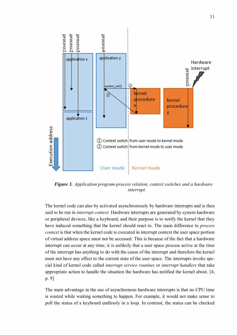
2.4.2 Process/kernel model
In modern operating systems the restriction of user space program access to kernel space
is enforced by hardware features. The hardware introduces two execution modes for the
CPU: a non-privileged mode (user mode) and a privileged mode (kernel mode) for user
programs and for the kernel, respectively. [5, p. 8]
This procedure is exploited in the process/kernel model, adopted by the Unix-like sys-
tems, where all the running processes have the illusion being the only process in the sys-
tem with exclusive access to OS services [5]. A process is a common abstraction for all
operating systems and it is defined as “an instance of program in execution” or as the
“execution context” of a program; a program can be executed concurrently by multiple
processes and a process can execute multiple programs sequentially, as seen in Figure 3.
[5, p. 8]
When user space application process makes a request to the kernel via a system call, the
execution mode is switched from user mode to kernel mode and the process continues to
execute a kernel procedure to fulfill its request. This way, the operating system is said to
act within the execution context of the process. Switches between user mode and kernel
mode are also called context switches. When the request is fulfilled, the hardware is forced
back to user mode and the process continues its execution from an instruction after the
system call. A context switch of a process is illustrated in Figure 3 with a process called
the “process4”. [5, pp. 10, 11]
11
Figure 3. Application program-process relation, context switches and a hardware
interrupt.
The kernel code can also by activated asynchronously by hardware interrupts and is then
said to be run in interrupt context. Hardware interrupts are generated by system hardware
or peripheral devices, like a keyboard, and their purpose is to notify the kernel that they
have induced something that the kernel should react to. The main difference to process
context is that when the kernel code is executed in interrupt context the user space portion
of virtual address space must not be accessed. This is because of the fact that a hardware
interrupt can occur at any time; it is unlikely that a user space process active at the time
of the interrupt has anything to do with the cause of the interrupt and therefore the kernel
must not have any effect to the current state of the user space. The interrupts invoke spe-
cial kind of kernel code called interrupt service routines or interrupt handlers that take
appropriate action to handle the situation the hardware has notified the kernel about. [4,
p. 9]
The main advantage in the use of asynchronous hardware interrupts is that no CPU time
is wasted while waiting something to happen. For example, it would not make sense to
poll the status of a keyboard endlessly in a loop. In contrast, the status can be checked

12
only when a button is pressed and an interrupt is generated by the keyboard, invoking an
interrupt handler taking appropriate actions [4, pp. 395-396]. How the interaction with a
peripheral device actually happens is a responsibility of a kernel device driver. The device
drivers are kernel programs that allow the kernel to interact with different kind of hard-
ware and they make the largest part of the Linux kernel sources [4, p. 471].
The Linux kernel is, of course, composed of many more different kind of components
and procedures to handle the running kernel; such as scheduling, the virtual file system,
process management and networking. This chapter was just to give the reader a brief
insight to the most important features for this thesis.

13
3. LINUX DEVICE DRIVERS
In an Unix system nearly every system operation is ultimately associated with a physical
device. Only with the exception of the processor, memory and some few other hardware
entities, all the device controlling is performed by device specific code called a device
driver and the kernel must include these pieces of code for every peripheral in the system.
This task is called device control, one of the main tasks of the Linux kernel. [9, p. 5]
The device drivers have a very special role in the kernel. They are the abstraction layer
making the hardware respond to an internal programming interface, consequently hiding
the hardware specific operation. This programming interface uses driver independent
standardized calls known as system calls and mapping these calls to interact with system
hardware is the main task of a device driver. The programming interface enables the driv-
ers to be built separately from the kernel and to be used only when needed by plugging
them into the kernel at runtime as modules. [9, p. 1]
In this chapter we have a brief look into different Linux device driver types and discuss
some common features a device driver needs to implement. Our understanding about the
Linux kernel is strengthened by looking into interrupt handling and memory management
features. Lastly, the single most important system hardware feature for the thesis is dis-
cussed; the direct memory access (DMA) operation.
3.1 Modules
Modules are software entities that can be dynamically added to a running kernel [9, p. 5].
The modules offer an efficient way adding functionality, for example device drivers and
filesystems, to the system kernel without the need of rebuilding the kernel or rebooting
the system [4, p. 473]. The dynamic loading of modules is carried out by the insmod
program that links the object file of a module into the kernel. Once linked, the object file
can be unlinked with the rmmod program [9, p. 5].
After a module is loaded to the kernel it waits to service future requests that can be in-
voked by other modules and processes. This approach is similar to the event driven pro-
gramming and while applications are not necessarily event-orientated, every module is.
Another difference to user applications is that while an application can be lazy on resource
release while exiting, a module needs to carefully release every resource it reserved at
initialization time. Otherwise these resources will linger in the system unsupervised until
the system is booted. [9, p. 18]

14
Modules also offer a convenient approach to device driver development. It would be time
consuming to rebuild the kernel – with the source code of the device driver under devel-
opment – every time a developer wants to test his/her modifications with the target plat-
form [9, p. 18]. Device drivers permanently compiled into the kernel are not covered in
this thesis because the implementation part only uses the module approach.
3.2 Device and driver types
A Linux system identifies its devices from three fundamental device types and utilizes
them by corresponding drivers [9, pp. 6-7]:
• Character device
A character device, commonly abbreviated as char device, is a device entity that
is interfaced as stream of bytes. Char devices are accessed via filesystem nodes,
one example being the text console (/dev/console). Usually a char driver imple-
ments at least system calls open, close, read and write. A char device behaves
much like a regular file in the filesystem but while one can move forward and
backward in a file, a char device usually acts as a data channel only enabling se-
quential access.
• Block device
A block device is an entity capable of hosting a filesystem and is also, like a char
device, accessed by a filesystem node under the /dev directory. An example of a
block device is a disk storage. In most Unix systems access to a block device is
restricted to whole blocks of 512 bytes, or a larger power of two, but in Linux any
number of bytes can be read and can be written to a block device. As result, a
block device looks exactly like a char device to the user. They differ only in the
way the kernel interfaces and manages the data of a block device and therefore
completely different interfacing implementation is needed for a block driver.
• Network interface
All network transactions are performed through a device capable of exchanging
data with another host and these devices are called interfaces. Usually these de-
vices are hardware devices but there is also pure software implemented interfaces,
for example the loopback interface. A network device is solely responsible for
sending and receiving data packets used in networking without knowing about the
connections and the networking subsystem in the kernel – one driving the network
device. Because a network interface is not a stream-oriented device, it is not easily
mapped to a node in a filesystem and the kernel uses packet transmission related
function calls to access a network device driver instead of read and write used
with char and block drivers.

15
It is not restricted to write a device driver implementing more than one these devices but
this is not considered as good practice. Writing a module implementing multiple devices
has negative effects on code scalability and extendibility. [9, p. 5]
Driver modules can also be classified by the functionality of devices they work on through
additional layers of kernel support subsystems. For example, every universal serial bus
(USB) device is controlled by a USB driver module that is a module working within a
USB subsystem. Nevertheless, the USB device shows up in the filesystem as a char device
or a block device in case the USB device happens to be a serial port or a USB memory
card reader, respectively. Furthermore, if the USB device is a networking device, like a
USB Ethernet adapter, it will show as a network interface. [9, p. 7]
3.3 Interrupt handling
As stated before, hardware interrupts are the way for peripheral devices to notify the pro-
cessor that something has happened and that the processor should act accordingly. This
functionality, called interrupt handling, is implemented by the device drivers. Basically,
the job of a driver is to register a handler function, called the interrupt handler, for its
device to take appropriate actions when the device generates an interrupt to the system.
These functions have some limitations on the actions they can perform due to the way
they are run in the Linux system. [9, p. 258]
The peripheral device slots include electronic lines to a component used to send interrupt
requests to a device called the interrupt controller. This controller then forwards these
requests to the interrupt inputs of the CPU. This way the peripheral devices are not actu-
ally able to force the interrupts on the CPU, but rather request them from the above com-
ponent and these requests are known as interrupt requests or IRQs. Each interrupt has a
unique number and a corresponding IRQ number that the kernel uses to look up an inter-
rupt handler associated with device responsible for the request. The conversion between
the IRQ number and the interrupt number is carried out by the interrupt controller and
often these terms are used interchangeably. [9, pp. 849, 850]
In case the processor receives an IRQ having no associating interrupt handler the kernel
simply acknowledges the interrupt and ignores it. The registration of a handler is expected
from the modules. The interrupt lines may also be shared between multiple modules, fol-
lowing a procedure called interrupt sharing. In both cases, the IRQ is requested by the
driver module with the request_irq() function, defined in <linux/interrupt.h>, which
should be called after the device is opened (used) for the first time and before the hard-
ware is allowed to produce interrupts. This is because of the limited amount of interrupt
lines. If the request for an IRQ would be issued at module initialization time, the driver
could waste this valuable resource if it is rarely used, especially if the driver does not
support interrupt sharing. [9, pp. 259, 261]

16
There are some restrictions implementing an interrupt handler that must be taken into
account. Because these handler functions are not run in the process context, they must not
change data between user space. The handlers also can never perform any actions that
could sleep, like a wait_event call, memory allocation with any other flag than
GFP_ATOMIC, or a semaphore locking. Furthermore, handlers cannot call the schedule()
function [9, p. 269]. This limitation originates from the fact that interrupt handlers should
always be executed in minimum amount of time; system malfunctions may occur if a
second interrupt is received while the first one is still being handled and it can lead to a
kernel deadlocking, in the worst case scenario. This can be avoided by disabling interrupts
during the handler execution but then interrupts essential for the system operation may be
lost and this approach is avoided whenever possible [9, p. 849]. Often the handlers, how-
ever, need to perform lengthy tasks in response to a device interrupt. Therefore the need
for minimal execution time and considerable work load conflict with each other. This
dilemma is resolved in Linux by splitting the interrupt handler into two halves called the
top half and the bottom half [9, p. 275].
If an interrupt handler is divided in two halves the one registered to an IRQ number with
the request_irq() is called the top half and is responsible for responding to an interrupt as
fast as possible. Before exiting, the top half schedules the more time consuming work to
be executed later, by the bottom half, at some safer time. In a typical use case the top half
saves data received from the interrupt responsible device to a buffer, schedules the bottom
half and exits. The bottom half can then perform the rest of the required work at some
later time. This could include awaking of a process in need for the buffered data or starting
a new I/O operation, for example. [9, p. 275]
The above procedure enables the top half to handle a new interrupt at same time the bot-
tom half is still executing. An example exploiting a common top half / bottom half divi-
sion is a network interface; the top half of an interface handler just retrieves the data on
arrival of a new packet and pushes it to the protocol layer for later processing by the
bottom half. The bottom half can be scheduled as a tasklet function or as a workqueue
function using the tasklet_schedule() and the schedule_work() functions, respectively.
The biggest difference between these two functions is that tasklets run in a software in-
terrupt context and the workqueues in the context of a special worker process, thus ena-
bling sleeping. Even though a workqueue runs in a process context it does not enable user
space data transfer. [9, pp. 275-277]
3.4 Memory allocation
Allocating memory in the kernel is not as easy as it is in user space programs. This is
because the kernel cannot easily deal with memory allocation errors and most of the time
cannot sleep while allocating memory. Due to these limitations allocating memory is
more complicated in the kernel than it is in user space. [10, p. 231]

17
The translations between virtual and physical memory is performed by a hardware com-
ponent called memory management unit (MMU). The MMU maintains the system’s page
tables in page-sized granularity. The size of a page varies between architectures and many
even support multiple page sizes. Majority of 32-bit and 64-bit architectures use 4 KB
and 8 KB pages, respectively. The kernel represents every physical page – or page frame
– with page structs, defined in <linux/mm_types.h>. These structs hold valuable infor-
mation of each page frame, one being the count of how many references there is in the
system to the page frame in question. [10, pp. 231-232]
The kernel provides multiple interfaces to perform memory allocation and ultimately all
of these interfaces allocate memory with page-sized granularity. Behind the scenes all the
interfaces for memory allocation use a low-level mechanism with a core function al-
loc_pages(), defined in <linux/gfp.h>, with its variants and corresponding memory free-
ing functions. The freeing functions must be carefully used only to free pages previously
allocated to avoid hanging the kernel, something that cannot happen in user space. [10,
pp. 235, 237]
3.4.1 Slab layer
Allocating and freeing different kind of data structures is a common operation inside the
kernel [10, p. 246]. Being limited only to page-sized allocations introduces a problem;
allocating full pages for small data structures leads to memory wastage. If a structure
composed of two 32-bit integer values is needed in the kernel code, allocating of a full
page of 4 KB for this structure would introduce unacceptable waste of memory [4, p.
257]. This problem causes the need for Linux to be able to handle smaller memory entities
than a page. One common solution is the slab layer.
The slab layer uses groupings called caches for different kind of object types like process
descriptors and inodes. These cachces are further divided into slabs that are composed of
one or more contiguous page frames and hold a number of equally-sized objects of cache
specified type. The slabs are marked as full, partial or empty, representing the availability
of objects in any given slab. The slab layer is managed by an interface exported to the
entire kernel, known as the slab allocator, enabling creation and destruction of new
caches and allocation and freeing objects from these caches. For example, obtaining an
object from a cache is requested with the kmem_cache_alloc() function, defined in
<linux/slab.h>. The kernel returns a pointer to already allocated, but unused object pri-
marily from a partial slab or secondarily from an empty slab. If no free objects are avail-
able, the slab layer internally creates a new slab using the kmem_getpages() function,
defined in <mm/slab.c>, which ultimately calls the kernel page allocator
__get_free_pages(). This way the management of caches and their associated slabs is
handled by the internals of the slab layer, as seen in the Figure 4. [10, pp. 246-249]

18
Figure 4. The slab allocator interfacing the slab layer subsystem, adapted from [10,
p. 247].
The slab layer works as sort of a specialized allocator for objects of cache specified type
and creation of new caches is supported by the slab allocator interface. Caches are desir-
able for objects that are frequently allocated and freed in the kernel. When the code needs
a new instance of a data structure defined by a cache it can simply grab one from a partial
slab without the need for memory allocation. After the code is done with the structure it
is released back to the slab, in contrast to memory deallocation. This way the slab layer
also works as a free list, enabling caching of frequently used structures increasing perfor-
mance and decreasing memory fragmentation2. [10, pp. 245-246, 249]
The slab layer also introduces a family of general purpose caches [10, p. 246]. The size
of objects inside these caches vary from 25 up to 225 bytes in length. The upper limit
can considerably vary between different architectures and systems [4, p. 261]. In an x86
or ARM based system, with the page size of 4 KB, a common upper limit is 4 MB, or
4 ∗ 220 B = 4 MiB to be exact [11]. These general purpose caches create the basis for
the kmalloc() function, the preferred interface for kernel allocations, implemented on
top of the slab layer alongside with the slab allocator. The slab caches of a given Linux
system are listed in the /proc/slabinfo utility. For example, the general purpose caches
of one ARM based Linux system are identified with a “kmalloc” prefix and are listed in
the Figure 5.
2 Memory fragmentation is a memory management problem where several page frames are free, but scat-
tered in the physical address space. Contiguous memory blocks are desirable for the system performance.
[4, p. 15]

19
Figure 5. The general purpose caches of an ARM based Linux system.
3.4.2 kmalloc()
The operation of the kmalloc() function, also defined in <linux/slab.h>, is similar to that
of malloc() routine used in user space memory allocation. The only exception is that
kmalloc() uses additional flags to indicate the type of memory requested and how it should
be allocated. The kmalloc() is the preferred interface for most memory allocations per-
formed in the kernel. [10, p. 238]
The kmalloc() function call uses two parameters: requested size of the memory in bytes
and gfp_t type flags defined in <linux/types.h>. The flags are divided in three groups [10,
pp. 238-239, 241]:
• Action modifiers
The action modifier flags tell the kernel how the requested memory should be
allocated. For example, if memory is allocated in interrupt context no sleeping is
allowed.
• Zone modifiers
The zone modifier flags specify the part of physical memory the allocation should
be performed on. In Linux, the physical memory is divided in four primary
memory zones with different kind of properties.
• Types
The type flags are combinations of action and zone modifiers for certain type of
memory allocations. This simplifies the process of providing the kmalloc() with
multiple flags as often only one type flag is needed.
The most common allocation of kernel memory is carried out in process context in a
situation that can sleep if necessary. A correct type flag for this case is the GFP_KERNEL

20
flag that is actually a combination of action modifiers __GFP_WAIT, saying that the al-
locator can sleep, __GFP_IO, saying that the allocator may start disk I/O and __GFP_FS
saying that the allocator can start filesystem I/O. Most of the time the zone modifiers are
not needed because the allocations can be made to any memory zone, as it is the case with
the GFP_KERNEL type allocation. Combining the modifiers into a type flag is just a
basic ORing operation. A kmalloc() function call
ptr = kmalloc(size, __GFP_WAIT | __GFP_IO | __GFP_FS);
is then equal to
ptr = kmalloc(size, GFP_KERNEL);
Another important type flag is the GFP_ATOMIC; it can be used in interrupt handlers
and bottom halves because it specifies an allocation that cannot sleep. [10, p. 242]
When the memory is allocated successfully the kernel returns a pointer to a physically
contiguous memory region that is at least the size requested. This is because the
memory is allocated from the slab layer subsystem’s general purposes cache; the re-
quested size is actually rounded up to the closest matching general purpose cache. If the
allocation should fail, a NULL pointer is returned. The memory allocated by the kmal-
loc() is released with the kfree() function. [10, pp. 238, 246]
3.4.3 vmalloc()
The biggest difference between the kmalloc() and the vmalloc() function, defined in
<linux/vmalloc.h>, is that while the kmalloc() allocates physically (and virtually) contig-
uous memory, the vmalloc() allocates memory that is only promised to be virtually con-
tiguous. This is also how the user space malloc() function works; the memory pages re-
turned are contiguous in the virtual address space of the processor but not necessarily in
the RAM. [10, p. 244]
On many architectures the hardware devices do not understand the virtual addresses be-
cause they reside – from the kernel point of view – behind the memory management unit,
thus requiring physically contiguous memory allocations in case they need to work with
memory locations. In contrast, memory regions used only by the software, like some pro-
cess-related buffers, can be just virtually contiguous. Still, the kmalloc() is the preferred
method allocating memory in the kernel and the vmalloc() is usually used only when
absolutely necessary. This is mainly due to the worse performance of the allocation; the
vmalloc() needs to work with page table entries to make physically noncontiguous page
frames contiguous in the virtual address space. [10, p. 244]
The vmalloc() is typically used in situations requiring a large portion of memory. For
example, modules are loaded into memory allocated with the vmalloc() [10, p. 244]. This
is because the allocation builds a virtual memory region by suitably editing free page

21
table entries, thus not being limited to the maximum size of any slab layer defined object
like the kmalloc(). In theory, the upper limit of the vmalloc() is the amount of available
RAM in the system [11].
Memory allocation with the vmalloc() might sleep and therefore it cannot be called from
interrupt context – or any other situation where blocking is not permitted. It only takes in
one parameter: the amount of desired memory in bytes. [10, pp. 244-245] If the allocation
is successful, a pointer to a virtually contiguous memory region, at least the size re-
quested, is returned and in case of an error a NULL pointer is returned instead. Because
the vmalloc() is page orientated, the allocation is actually rounded up to the nearest whole
amount of pages. The memory allocated by the vmalloc() is released with the vfree() func-
tion. [9, pp. 225-226]
3.4.4 ioremap()
In some situations physical memory outside the address range of the kernel page tables is
allocated for devices at boot time. This can be the case, for example, with a PCI (periph-
eral component interconnect) video device’s frame buffer. For a driver to be able to access
this already allocated buffer it can call the ioremap() function that like vmalloc(), builds
new page tables. But, unlike the vmalloc(), it does not allocate any memory but returns a
special virtual address that enables access to a specified physical address range. This ad-
dress should not be used to directly access memory as it was a pointer. Rather, specialized
I/O functions, like the readb(), should be used with the address retrieved by the ioremap().
This address is released by the iounmap() function.
3.5 Direct memory access
DMA is a hardware operation allowing system peripherals to transfer their data to and
from the system memory without any need for processor intervention. Systems periph-
erals capable of such operation are also known as DMA controllers. Because using this
method can eliminate much computational overhead, it can greatly increase the system
performance and the data throughput. [9, p. 440]
The DMA transfer from a device can happen in two different ways; either the software
asks the device to transmit data or the device asynchronously writes data to the system.
The first case can be summarized in following steps [9, p. 441]:
1. A process calls the read system call of a device and the driver of the DMA capable
device instructs the device to transfer its data to a pre-allocated DMA buffer. The
process that invoked the read is put to sleep.
2. The DMA capable device writes its data to the buffer and generates an interrupt
after it is done.

22
3. The interrupt handler of the driver awakens the process put to sleep in step 1,
which is then able to read the data.
In the second scenario the DMA controller usually expects to have access to a circular
buffer, also called a ring buffer, to write its data asynchronously to a next available buffer
in the ring and raises an interrupt to notify that there is now data available in the ring. [9,
p. 441].
3.5.1 DMA Mapping
Using DMA operations is ultimately based on allocating a buffer and passing it to a DMA
capable device. Allocating a DMA buffer is possible with the kmalloc() or the
get_free_pages() functions. If the DMA capable device is known to be limited to 24-bit
addressing, like the ISA (industry standard architecture) devices, a GFP_DMA type flag
needs be passed to the allocator, forcing the allocation to happen from a DMA memory
zone that is addressable with 24-bits. [9, pp. 442-444]
However, a DMA capable device, connected to some interface bus, uses physical ad-
dresses, unlike the program code allocating the buffer. Actually, the device uses bus ad-
dresses, rather than physical addresses, because in some architectures the interface bus is
connected to special circuitry that converts I/O addresses to physical addresses. It takes
some special functions to convert the virtual address returned by an allocator to a bus
address. Using these functions is strongly discouraged. The correct way is to use a generic
DMA layer, offered by the Linux system, which handles the conversion. [9, pp. 442-444]
The generic DMA layer offers a bus- and architecture-independent approach creating a
device driver utilizing hardware capable of DMA operations. It includes a mapping oper-
ation, called a DMA mapping, which generates the bus address usable by the device from
the allocated buffer. Through these mappings also cache coherency can be managed.
Cache memory is a feature found in modern processors that stores copies of recently used
memory locations in a CPU cache, boosting system performance. This may introduce
problems, however, if main memory is accessed without the CPU knowing about it, as it
is with the DMA operation. [9, pp. 445-446]
The generic DMA layer is interfaced by the DMA API (application programming inter-
face) defining the needed DMA mapping functions in <linux/dma-mapping.h>. The
DMA API introduces two different kinds of mappings: consistent, also known as coher-
ent, and streaming DMA mappings. The consistent mapping automatically takes care
about the cache coherency problem so that the device and the CPU both see the updates
they make without any software flushing operations. In contrast, the streaming DMA
mapping requires the user to take care of flushing the cache. The interfaces for this map-
ping type were designed in a way that they can fully utilize whatever optimization the

23
hardware allows. DMA mapping can be performed with the dma_alloc_coherent() (con-
sistent) and the dma_map_single() (streaming) functions and unmapping with the
dma_free_coherent() and the dma_unmap_single() functions, respectively. On success,
they both return a dma_addr_t type DMA handle that is usable by the DMA device. In
case of the streaming mapping, the cache coherency must be taken care of by calling the
dma_sync_single_for_cpu() and the dma_sync_single_for_device() functions accord-
ingly. [12]
In case very small DMA mappings are required, the user should consider using a DMA
pool. The DMA pool, defined in <linux/dmapool.h>, is an allocation mechanism for
small, consistent mappings. The mappings performed by the dma_alloc_coherent() may
be limited to minimum size of one page and in case the driver needs smaller DMA areas,
a DMA pool should be used [9, p. 447]. A DMA pool works much like the slab allocator,
but instead of using the get_free_pages() function it uses the dma_alloc_coherent() inter-
nally [12].
The above discussed streaming type DMA mapping methods requires physically contig-
uous memory allocated by the kmalloc() or the get_free_pages() functions. In some situ-
ations, however, the buffers needed in the DMA can reside different parts of the physical
RAM. They could be mapped individually and then the DMA operations could be se-
quentially performed on each buffer. This problem is resolved by a special type of stream-
ing DMA mapping called the scatter/gather mapping. Many DMA controllers accept so
called scatterlists, consisted of array pointers and lengths, and transfer everything in the
list as one DMA operation, introducing better performance. In a system that uses map-
pings between bus addresses and page frames, a scatterlist can also be arranged in a way
that discontiguous page frames look contiguous to the device. The scatterlist is defined in
<asm/scatterlist.h>. [9, p. 450]
After the scatterlist is created, the scatter/gather mapping is carried out by the
dma_map_sg() function taking in the scatterlist as one of the parameters. If the system
has an I/O memory management unit (IOMMU), the dma_map_sg() programs the unit’s
mapping registers so that, in the best case scenario, the device thinks that one block of
contiguous memory was received. Because the scatter/gather is a type of streaming DMA
mapping, the user needs to take care of cache coherency by calling the
dma_sync_sg_for_cpu() and dma_sync_sg_for_device() functions accordingly. A scat-
ter/gather mapping is released with the dma_unmap_sg() function. [9, p. 451]

24
4. FPGA BASED SOC-PLATFORM
A computer, with all its components, or some other electronic system implemented on a
single integrated circuit can be referred to as a system-on-a-chip (SoC). Figure 6 shows
an example of a typical SoC system illustrated in functional blocks connected with some
system bus architecture. In addition to a processor and embedded memory units, a typical
SoC includes some communication peripherals, like wired USB connections or wireless
communication ports, a PLL (phase-locked loop) for system timing, data conversion
blocks like analog-to-digital (A/D) and digital-to-analog (D/A) converters and digital sig-
nal processor (DSP) circuits. [13, p. 5]
Figure 6. Functional block diagram of a typical SoC circuit, adapted from [13, p.
4].
A common task for a SoC based system is digital signal processing application such as
imaging, software defined radio or a radar. The algorithms needed in digital signal pro-
cessing can be very demanding in the means of processing power and traditionally these
algorithms are run on dedicated components called digital signal processors (DSP) [14,
pp. 4-5]. This operation is known as hardware acceleration, where some specific func-
tions of an application, with high performance demands, are performed with hardware

25
components instead of the CPU [6, p. 9]. The DSPs can also be replaced with more gen-
eral purpose circuits known as FPGAs (Field programmable gate array). A modern FPGA
has a capability to be programmed to perform just about any digital operation imaginable
and they can outperform the fastest DSP chips by a factor of 500 or more. Due to their
lowering price and high usability the FPGAs are becoming increasingly attractive for em-
bedded system applications [14, p. 5].
The demands for the SoC hardware are, of course, application specific and the hardware
and the software should be considered as a whole when designing an embedded system.
Especially in low production volume products it is often desirable to keep the custom
hardware development at minimum and to use verified commercial components. Further-
more, in high performance applications demanding hardware acceleration, a SoC contain-
ing a FPGA circuit may be a cost-effective choice.
In this chapter some common FPGA architecture features are discussed and the SoC plat-
form used in the implementation part of the thesis is presented.
4.1 Field programmable gate arrays
The field programmable gate arrays are digital integrated circuits (IC) containing pro-
grammable logic blocks, connected by configurable interconnects, enabling such devices
to be programmed to perform various, user defined, tasks. The “field programmable” part
of the name refers to the fact that FPGA’s are programmable “on the field”, in contrast to
devices configured by manufacturer. [14, p. 1]
While FPGAs do not necessarily offer the fastest available clock rate among ICs, it may
be possible to achieve superior performance due to their parallel architecture, especially
suitable to signal processing applications. Still, a specialized hardware component often
outperforms a FPGA. The greatest advantage FPGAs bring to system design is flexibility.
It is their reconfigurability capabilities together with the high processing power that
makes FPGAs considerable choice in many applications. [15, p. 8]
4.1.1 FPGA comparison to other ICs
Other kind of “in field” programmable ICs do exist; PLD’s (programmable logic device)
also have manufacturer defined architecture but are programmable by the end user to
perform different kind of functions. These devices, however, contain relatively limited
number of programmable logic, therefore only being capable of small and simple func-
tions [14, p. 2]. Because of this limitation, the PLD manufactures developed CPLDs
(complex programmable logic device), which can be thought as multiple PLDs in a single
chip, connected by a programmable interconnect. These devices actually have some over-
lap with the FPGAs in potential applications. FPGAs still tend to outperform CPLDs in
register-heavy, pipelined applications and in applications dealing with high speed input

26
data streams. Additionally, FPGA’s architecture is more flexible and usually offers a
denser circuit (more gates in a given area) and they have become the industry standard,
or “de facto”, in large programmable logic designs [1, pp. 244-246].
In contrast to “in field” programmable ICs there are ASICs (application-specific inte-
grated circuit) and ASSPs (application-specific standard part). These circuits can contain
hundreds of millions logic gates and carry out extremely large and complex functions.
Both of these circuits are based on the same manufacturing processes and they are both
custom-designed to serve some specific application, the only difference being that ASICs
are designed and built for a specific company, but ASSPs are marketed to multiple cus-
tomers. These circuits both overcome FPGAs in the number of transistors, complexity
and performance. On the downside they are very expensive and time-consuming to de-
velop and they are not reconfigurable after they are built.
FPGA features lie in between of those introduced by CPLDs and ASICs; they are recon-
figurable like PLDs, but can contain millions of logic gates, enabling implementation of
large and complex designs, like ASICs. In comparison to ASICs the design changes and
overall development is easier and faster with FPGAs leading faster time to market. The
FPGAs are also cheaper to develop; no expensive toolsets for ASIC designs are required
and developers may test their hardware and software designs on FPGA-based test plat-
forms, without the need for non-recurring engineering. On the other hand, after develop-
ment, ASIC circuits are cheaper to produce and this is especially notable in large scale
production. [14, pp. 2-3]
FPGAs can also be used in prototyping. Since it is cheaper and faster to develop an ap-
plication, in need for hardware accelerated parts, with a FPGA circuit, the product may
be developed using a FPGA and later produced with an ASIC [1, p. 245]. The choice
between FPGAs and ASICs eventually comes down to tradeoffs between development
and production costs, demands on time to market and future product support and devel-
opment needs. The FPGA circuits become especially favorable in low volume projects
with fast time to market needs and limited development resources.
4.1.2 General FPGA architecture
The FPGAs consist of an array containing varying type and number of programmable
logic blocks such as general logic, multiplier and memory blocks. These blocks are con-
nected by a configurable routing fabric so that different blocks can be programmably
interconnected. The array is connected to the outside world through surrounding program-
mable I/O blocks. This general structure is illustrated in the Figure 7. [16, p. 3]

27
Figure 7. General FPGA structure, adapted from [16, p. 3].
These logic blocks are built from more basic elements, often called logic cells (LC) or
logic elements (LE), depending on the vendor. An LC could, for example, consist of a
LUT (lookup table) with 4 bit wide input, a multiplexer and a register. A LUT is also
capable of acting as a 16x1 bit RAM element or a 16-bit shift register and the register can
be configured as a flip-flop or as a latch. When configured as a flip-flop (clocked register),
the register can also be configured to be triggered by a rising edge or by a falling edge of
an input clock signal [14, p. 74]. A simplified version of an LC, with a flip-flop configured
register, can be illustrated with the Figure 8. It should be noted that this assembly is just
an illustration of a simplified LC architecture. Actual architecture of these low-level
FPGA elements may differ even between different device families from the same vendor
and in advanced FPGA families the internal structure of these elements can be quite com-
plicated [15, p. 25].

28
Figure 8. A simplified LC element, adapted from [14, p. 74].
The LUT seen in Figure 8 can be used to implement a Boolean function with 4 or fewer
inputs and the output of the LUT can be fed out of the LC or into a register through a
multiplexer [15, p. 25]. For example, the LUT could be configured to perform the fol-
lowing Boolean function:
y = (a & b) | (!c | d)
, where “&” is used as logical AND, “|” as logical OR and “!” as logical NOT operator.
This function can also be represented with graphical logic gates as illustrated in Figure
9.
Figure 9. A Boolean function represented by graphical logic gates.
The Boolean function can be configured into the LUT as seen in Table 1.
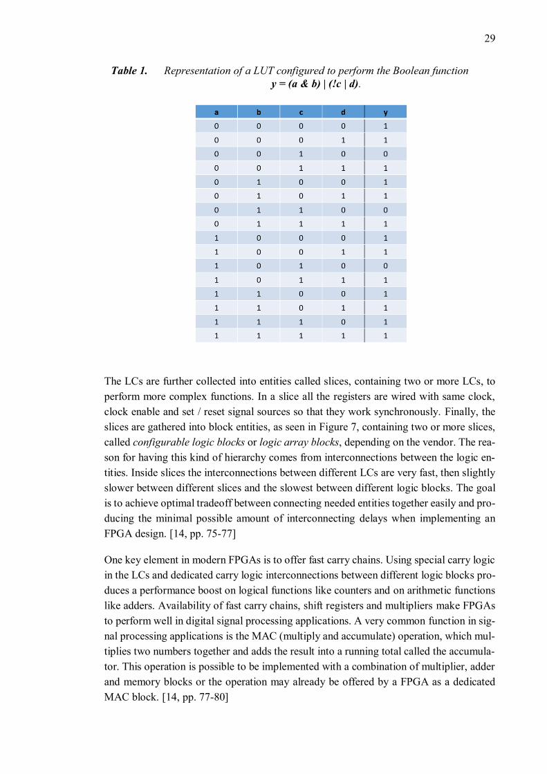
29
Table 1. Representation of a LUT configured to perform the Boolean function
y = (a & b) | (!c | d).
The LCs are further collected into entities called slices, containing two or more LCs, to
perform more complex functions. In a slice all the registers are wired with same clock,
clock enable and set / reset signal sources so that they work synchronously. Finally, the
slices are gathered into block entities, as seen in Figure 7, containing two or more slices,
called configurable logic blocks or logic array blocks, depending on the vendor. The rea-
son for having this kind of hierarchy comes from interconnections between the logic en-
tities. Inside slices the interconnections between different LCs are very fast, then slightly
slower between different slices and the slowest between different logic blocks. The goal
is to achieve optimal tradeoff between connecting needed entities together easily and pro-
ducing the minimal possible amount of interconnecting delays when implementing an
FPGA design. [14, pp. 75-77]
One key element in modern FPGAs is to offer fast carry chains. Using special carry logic
in the LCs and dedicated carry logic interconnections between different logic blocks pro-
duces a performance boost on logical functions like counters and on arithmetic functions
like adders. Availability of fast carry chains, shift registers and multipliers make FPGAs
to perform well in digital signal processing applications. A very common function in sig-
nal processing applications is the MAC (multiply and accumulate) operation, which mul-
tiplies two numbers together and adds the result into a running total called the accumula-
tor. This operation is possible to be implemented with a combination of multiplier, adder
and memory blocks or the operation may already be offered by a FPGA as a dedicated
MAC block. [14, pp. 77-80]

30
4.1.3 FPGA clocking
All synchronous elements in the FPGA, like the registers configured as flip-flops inside
an LC element, needs to be driven by a clock signal. Typically, clock signals are taken
into the FPGA fabric from outside world through a dedicated clock input pins, from which
they are routed to different parts of the fabric via specialized clocking tracks called clock
trees. The name clock tree comes from the fact that the clock tracks are divided into
branches finally leading to the registers in different parts of the FPGA. This branching
structure is used to ensure that different registers can see the rising (or falling) edges of
the clock signal as simultaneously as possible. In contrast, if the clock signal should be
distributed to the registers sequentially through a single line, the first register on the line
would see the edges of a clock much sooner than the last one. This time shift in edge
detection between registers is called clock skew and it cannot be fully compensated, even
with clock trees. The clock trees are also called clock domains because different clock
trees, on the same FPGA circuit, can be used with varying frequency clocks. [14, pp. 84-
85]
The clock input pins are often not directly connected to the clock trees but to a specialized
clocking blocks called clock managers, which can be used to generate multiple different
kind of clock signals from a single source. These generated clock signals can then be
distributed to clock trees or to clock capable output pins, back to the outside world. The
clock managers can be used to generate faster or slower clocks from the input clock, or
phase shifted clocks with the same frequency. The clock managers are based on phase-
locked loops (PLL) or digital delay-locked loops (DLL). [14, pp. 85-89]
An FPGA design implementing multiple clock domains introduces complex timing re-
quirements especially in situations where data is changed between clock domains. The
design complexity further grows if multiple FPGAs are to be used synchronously with
strict timing requirements. This kind of situations demand careful designing and
knowledge on more advanced topics like clock domain crossing circuitry.
4.1.4 FPGA programming
All FPGA circuits are either reprogrammable or one-time programmable devices and
every FPGA circuit needs to be programmed at some point of the implementation process
to give them their functional operation. Four different kind of programming technologies
exist to configure a FPGA circuit [15, p. 22]:
• SRAM (Static RAM) based
An external device such as a nonvolatile memory or a microprocessor is
used to program the FPGA on power up. The configuration of the FPGA is
volatile. Fast in-chip reprogramming is possible.

31
• Anti-fuse based
The FPGA configuration is programmed by setting (burning) internal fuses
to achieve the desired operation. The configuration is nonvolatile but cannot
be reprogrammed.
• EEPROM / EPROM ((electrically) erasable programmable read-only
memory) based
The configuration is nonvolatile and similar to that of EEPROM / EPROM
devices. The device must be programmed off board (out of circuit).
In modern FPGAs the SRAM based programming has become the most widely used tech-
nology and it is used in devices by vendors like Xilinx, Lattice and Altera, all being in
the top five of biggest companies in the FPGA market [16, pp. 9, 16] [15, p. 23]. The
reconfigurable SRAM based FPGAs are in many case the best choice in development and
especially in prototyping projects. This is because the FPGA design will often change
numerous times in the life cycle of such project. The other technologies can have appli-
cations with stable and well-tested designs [15, p. 23].
A SRAM based FPGA is programmed with a configuration data, often called a bitstream,
usually loaded from an external nonvolatile memory unit. The bitstream can also be di-
rectly written by a processor, or downloaded from a PC and it takes at most a few hundred
milliseconds to complete the configuration of the FPGA. The programming time depends
on the size of the used FPGA circuit, implemented configuration interface and speed of
the configuration data transfer. The configuration time is often tolerable when considering
the benefits of dynamical in-chip reconfiguration and this especially the case when other
system devices requiring a boot-up, like the processor, are used. [15, p. 22]
The bitstream, used to configure a FPGA, is generated by a following general workflow
[15, p. 104]:
1. FPGA design is created with HDL (hardware description language) like VHDL
(VHSIC hardware description language) or Verilog.
2. A verified design is synthetized, analyzed and optimized for target circuit by ven-
dor provided tools.
3. Synthetized design is mapped (placed) and routed on the target circuit model, after
which bitstream is generated, by vendor provided tools.
4.2 Xilinx Zynq-7000 devices
In the implementation part of this thesis a device from the Zynq-7000 All Programmable
SoC family, by Xilinx, was used. Xilinx has been the FPGA market leader for more than
a decade and the Zynq-7000 family offers top end performance-per-watt devices with one
of the best quality-price ratios on the market, making it a viable choice in many embedded

32
applications [17] [18, p. 1]. These SoCs are promoted to offer an flexible alternative to
traditional ASIC based solutions.
The SoCs in the Zynq-7000 family are divided in cost-optimized Zynq-7000S and per-
formance-per-watt optimized Zynq-7000 devices embedding single-core and dual-core
ARM Cortex™-A9 processors, respectively. All Zynq-7000S devices include the Artix-
7 FPGA and the high end of Zynq-7000 devices use the Kintex-7, industry leading, FPGA
circuit [18, p. 1]. The processor side of the SoC platform is referred to processing system
(PS) and the FPGA side to programmable logic (PL). Some key features of the Zynq-
7000 devices are listed in the Table 2.
Table 2. Key features of Zynq-7000 SoCs, adapted from [19, pp. 1-2, 7, 13, 14].
Processing system (PS) Programmable logic (PL)
ARM Cortex-A9 Based Application processing unit (APU)
• 2.5 DMIPS/MHz per CPU
• Up to 1 GHz CPU frequency
• ARMv7-A architecture
• Integrated MMU
Configurable Logic Blocks (CLB)
• Four LUTs (with 6-bit input), and eight flip-flops (of which 4 is configurable as latches) per slice
• Two slices per CLB
• LUTs configurable as 64x1 or 32x2 bit RAM or shift registers
On-Chip Memory
• On-chip boot ROM
• 256 KB on-chip RAM o Accessible by CPU and PL
Block RAM
• 36 Kb blocks
• Configurable as dual 18 Kb block RAM
External Memory Interfaces
• 16-bit or 32-bit interfaces to DDR3, DDR3L, DDR2 and LPDDR2
• 8-bit SRAM data bus with up to 64 MB sup-port
DSP Blocks
• 18 x 25 signed multiply
• 48-bit adder/accumulator
8-Channel DMA Controller
• Memory-memory, memory-device, device-memory and scatter-gather support
• 4 channels dedicated to PL
Programmable I/O Blocks
• Supports LVCMOS, LVDS, and SSTL
• 1.2V to 3.3V I/O
• Programmable I/O delay and SerDes
I/O Peripherals and Interfaces
• 2x 10/100/1000 Ethernet interface
• 2x USB 2.0 interface
• 2x SD/SDIO 2.0/MMC3.3 controllers
• 2x high-speed UART (up to 1 Mb/s)
• 54 bits GPIO
Low-power serial transceivers (in selected devices)
• Up to 16 receivers and transmitters
• Up to 12.5 Gb/s data rate
Interconnect (ARM AMBA AXI)
• High-bandwidth connectivity between PS and PL
2x 12-Bit Analog-to-Digital Converters
• Up to 17 external differential input channels
• One million samples per second maximum conversion rate

33
With the application processor the Zynq-7000 devices enable the use of high level oper-
ating system such as Linux and other standard operating systems available for the ARM
Cortex-A9 processor. Xilinx offers already implemented Linux device drivers for the PS
and PL peripherals for rapid product development and the use of ARM-based PS intro-
duces a range of third-party tools and IP (intellectual property). The Xlinx PS-PL SoC
solution promises a high level of performance that a two-chip solution could not match
because of their latency, higher power consumption and limited I/O bandwidth. [19, p. 5]
The Zynq-7000 devices introduce dedicated DSP slices consisted of a 25 x 18 bit two’s
complement multiplier and a 48-bit accumulator well suited for digital signal processing
applications. These slices, operating up to 741 MHz, combine high speed with small size
and flexibility. In addition to signal processing applications they behave well in applica-
tions such as dynamic bus shifters and memory address generators. [19, p. 17]
4.2.1 PS-PL interfacing
In order to use the FPGA in hardware acceleration tasks a data and signal transfer between
PS and PL is required. The Zynq-7000 family SoCs provide multiple interfaces to match
the application specific needs. These interfaces include [19, p. 12] [20, p. 40]:
• AMBA AXI interfaces
o Two 32 bit AXI general purpose master interfaces (AXI_GP)
o Two 32 bit AXI general purpose slave interfaces (AXI_GP)
o Four high-performance AXI ports (AXI_HP)
▪ 64/32 bit configurable
▪ Buffered
▪ Direct access to DDR and to OCM (on-chip memory)
o One 64 bit AXI slave interface (AXI_ACP)
▪ Coherent access to CPU memory
• DMA, interrupts, event signals
o Processor event bus for signaling event information to the CPU
o PL to PS interrupts
o Four DMA channels
o Asynchronous triggering signals
• Clocks and resets
o Four PS clock outputs to the PL
o Four PS reset outputs to the PL
• Configuration and miscellaneous
o Processor configuration access port
▪ Full and partial PL configuration
▪ Image decryption and authentication in secure boot
o RAM signals from the PL to the PS

34
o XADC interface
o JTAG interface
The AMBA (Advanced microcontroller bus architecture) is a bus architecture interface-
able by AXI (Advanced eXtensible interface) protocol compatible system modules, both
developed by Arm Holdings Ltd. The AXI protocol offers support for high-performance,
high-frequency systems and is suitable for high-bandwidth and low-latency designs. The
latest AXI protocol interface is called AXI4, which also provides a simpler control regis-
ter interface, known as AXI4-Lite, for applications not in need for the full AXI4 specifi-
cation. The AXI protocol is burst based and defines 5 independent transaction channels
for communication: [21, pp. x, A1-20, A1-21]
• Read address
• Read data
• Write address
• Write data
• Write response
Furthermore, the AMBA 4 specification introduces a streaming AXI interface called the
AXI4-Stream protocol. It is used as a standard interface between master/slave compo-
nents that need to exchange data. The AXI4-Stream protocol does not use addresses but
signals related to a handshake process between the master and slave component. [22, pp.
1-2, 2-3]
The highest performance in the means of data transfer is provided by the high perfor-
mance AXI (AXI_HP) ports and the ACP port. The high performance AXI ports are usu-
ally used in applications with high throughput between the PS and the PL. When using
the HP ports, the cache coherency, if needed, needs to be managed by software. The four
HP ports provide access from the PL to the DDR or OCM of the PS and they can be
configured as 32-bit or 64-bit interfaces. If the CPU memory needs to be accessed by
hardware, the ACP port should be used. [19, p. 13]
Through these ports it is possible to read data to the PS from a PL implemented block
RAM (BRAM), for example. If the data throughput is high, like in many digital signal
processing applications, this approach will produce high stress on the CPU. More delicate
way is to use the DMA operation covered in chapter 3.5.
4.3 FPGA based DMA transfer
The Zynq-7000 family SoCs include a dedicated DMA hardware component called the
DMAC (Direct memory access controller), which is an ARM developed AMBA periph-
eral. It is capable of performing data transfers between system memories and PL periph-
erals. However, only PL peripherals connected to the AXI_GP interface are accessible by

35
the DMAC and this port does not offer as good performance as the AXI_HP port. [20,
pp. 251, 256]
As stated before, the FPGA circuits can be programmed to perform almost any imaginable
digital operation and the DMA operation makes no exception. Xilinx offers wide support
of “soft” IPs for the Zynq-7000 family. A “soft” IP is used to describe a software entity,
in contrast to hardware or “hard” IPs. One of these Xilinx’s soft PL IPs, referred as Xilinx
LogiCORE™ IP, is the AXI Direct Memory Access (AXI DMA) core. The AXI DMA
core provides a high-bandwidth DMA between the system memory and AXI4 Stream
compatible peripherals, through the AXI_HP port. [23, p. 4]
The AXI DMA core is a software component written in VHDL (VHSIC hardware de-
scription language). It supports three different kind of execution modes: direct register
mode (simple DMA), scatter/gather mode and a cyclic DMA mode. The core is controlled
through 32-bit wide control registers and each mode requires specific programming se-
quence of the registers [23, pp. 68-72]. These register manipulations may be performed
directly from the code but Xilinx also supports the core with a standalone bare-metal C
software and with a Linux device driver. This driver is written in respect to the generic
DMA layer, thus enabling the use of DMA API in a custom, application specific driver.

36
5. DATA TRANSFER OPTIMIZATION
Traditionally, when data is transferred between system devices it is the system processor
that is in charge for this operation; the processor reads the data from a device and writes
it to another sequentially one word or a byte at a time. This is practical procedure with
low data volumes and rates, but if the amount of data to be transferred is large or the data
rate of the transfer is high, the overall system performance will decrease. [1, p. 105]
This thesis aims to further enhance a project using a Zynq-7000 SoC based system that
transfers high volumes of data from the FPGA chip to the PS running a custom Linux
distribution. The initial solution used CPU accessible BRAM blocks implemented on the
PL. The problem was that the method used high amount of CPU time just for fetching the
data from the PL to the PS, via the AMBA bus, before later manipulation of the data. The
initial solution also utilized high amounts of FPGA resources to implement the BRAM
blocks. A working DMA based data transfer solution was implemented but it still contains
some processor demanding parts and further optimization of the data transfer was re-
quired for future applications with even higher data rates.
In this chapter a DMA test system is constructed for evaluating the data transfer and all
of its components are introduced. Two optimization architectures are then discussed and
one of these methods is implemented.
5.1 Test system components
A test system was implemented on a MicroZed development board by Avnet including a
Z-7010 SoC, from the Zynq-7000 family, to test the FPGA based DMA capabilities. The
basic idea of the system is to generate pre-defined data from a PL implemented source,
transfer this data to the PS using a DMA controller and finally verify the data in a user
space test program. High level overview of the implemented system can be seen in the
Figure 10.

37
Figure 10. The implemented DMA test system on a Z-7010 based MicroZed
board.
The test system consist of 4 major entities:
• Programmable logic (PL)
o Sample generator (Verilog)
▪ Counter data generation
▪ Dynamically configurable TLAST signal positioning
▪ Dynamically configurable clock divider value
▪ Dynamic error insertion to the AXI4-Stream
▪ VHDL test bench simulation sources
o AXI Direct Memory Access (7.1) (VHDL)
▪ Soft IP block by Xilinx
▪ Write and read channels (S2MM and MM2S)
▪ Scatter/gather capability
▪ Offers a Linux device driver enabling the use of Linux DMA layer
• Processing system (PS)
o AXI DMA Cyclic (C, Linux kernel module)
▪ Utilizes the Linux DMA layer
▪ Implements a DMA ring buffer
▪ Controls the sample generator core
▪ Registers as a char device

38
▪ Implements an IOCTL (input/output control) system call interface
for user space access
▪ Implements open, close, read system calls
o DMA Test (C, user space test program)
▪ Opens the char device registered by the kernel module
▪ Performs read system calls and validates the data
▪ Uses the IOCTL system calls for non-standard communication
with the module
▪ Writes a log of the test results
The data transfer project used corresponding components that were used as base for the
implementation of the test system entities. The sample generator was initially written in
VHDL but it did not include all the capabilities provided by its Verilog counterpart. The
kernel module was stripped from functionalities not needed in the DMA test system and
some test related functionality was added. Also the user space test program was modified
in this way. Only the AXI DMA core was taken straight from the initial design.
The source of the sample data, the sample generator, implements the AXI4-Stream pro-
tocol defined by the AMBA 4 AXI4-Stream Protocol specification and writes the gener-
ated samples to this stream interface connected to the AXI DMA core. The samples are
then transferred by the AXI DMA through the AXI_HP interface to the DRAM (dynamic
random-access memory) controller of the PS, which writes the data to a ring buffer allo-
cated by the axi_dma_cyclic.c module. The samples are requested by a user space test
program dmatest.c that performs the read system call on a char device (/dev/dmatest),
registered by the axi_dma_cyclic.c module.
The PL cores are controlled through a general purpose GP interface, which is split in two
in the Figure 10 just for clarity. The figure does not include all low-level software and
hardware components but just the essential parts to understand the overall working of the
test system.
5.1.1 Sample generator
The sample generator is a custom programmable logic core implemented in hardware
description language Verilog. It generates the sample data that is finally received by the
dmatest.c user space test program. The data originates from a 32-bit counter register in-
cremented on every rising edge of a software generated clock named as the sample clock.
The sample clock is generated from the FPGA common clock by toggling the sample
clock on every Nth rising clock edge of the common clock, N being a natural number
bigger than 1. Lastly, the sample generator implements the AXI4-Stream protocol driven
by the common FPGA clock; every time the counter register is incremented, the new
value is pushed to the stream and to the AXI DMA core.

39
The sample generator consists of two submodules: the sample clock generator and the
counter data generator modules. The inputs, outputs and shared connections of these mod-
ules can be seen as a graphical representation in the Figure 11. The AXI4-Stream interface
is implemented at the top level of the sample generator.
Figure 11. The sample generator submodules as graphical blocks.
The sample clock is derived from the common FPGA clock ACLK by calculating the
rising edges and toggling the output according to the clk_divider input value specified by
the user. The toggling circuit implementation of the sample_clk_gen can be seen in Pro-
gram 1 and the whole module in Appendix A.
The sample clock is used in the counter data generator so that every time the state of the
clock changes from 0 to 1 a counter register is incremented and the data_valid register is
set to 1 for one ACLK clock period. The data generation circuit is clocked by the faster
1 2 3 4 5 6 7 8 9 10 11 12 13 14 15 16 17 18 19 20 21 22 23 24 25 26
always @(posedge ACLK) begin // Synchronous reset if(~ARESETN) begin sample_clk <= 1'b0; end else begin // The clk divider needs to be at least 2 // for the sample clock generation if(clk_divider > 1) begin // Count the ACLK positive clock edges if(counter_r < (clk_divider - 'd2)) begin counter_r <= counter_r + 'd1; end // Toggle the sample clock state else begin counter_r <= 'd0; if(sample_clk == 1'b0) begin sample_clk <= 1'b1; end else begin sample_clk <= 1'b0; end end end end end
Program 1. The sample clock generation circuit of the sample_clk_gen module.

40
ACLK clock. This is possible because the two clocks are synchronous. The data genera-
tion circuit implementation can be seen in the Program 2 and the whole module in Ap-
pendix B.
AXI4-Stream interface
The sample data increment can be seen on the line 19 of the counter data generator circuit.
This value is pushed to the AXI4-Stream implemented on the top level of the sample
generator. The AXI DMA core is interfaced with AXI4-Stream using 5 signals:
TREADY, TVALID, TLAST, TDATA and TKEEP. The AXI4-Stream protocol using 5
signals can be illustrated as a wave diagram seen in Figure 12.
1 2 3 4 5 6 7 8 9 10 11 12 13 14 15 16 17 18 19 20 21 22 23 24 25 26 27 28 29 30 31
always @(posedge ACLK) begin // Synchronous reset if(~ARESETN) begin sample_data <= 'd0; data_valid <= 1'b0; trigger_sample_write <= 1'b1; end else begin // Allow the data_valid only for one ACLK clock cycle if(data_valid) begin data_valid <= 1'b0; end // If sample generator is enabled if(enable) begin // If the sample clock is asserted and // no sample data has been written on this positive // sample clock cycle if(sample_clk && trigger_sample_write) begin sample_data <= sample_data + 'd1; data_valid <= 1'b1; // Wait for next positive sample clock cycle trigger_sample_write <= 1'b0; end else if(~sample_clk) begin // Trigger sample write on next positive // sample clock cycle trigger_sample_write <= 1'b1; end end end end
Program 2. The counter data generator circuit of the count_data_gen module.

41
Figure 12. An AXI4-Stream wave diagram with 5 signals and counter data
payload, adapted from [24, p. 86].
Before a transfer can begin, the slave (AXI DMA) needs to set the TREADY signal indi-
cating that the slave is ready to accept transfer. After the signal is set, the master can write
data to the stream via the TDATA bus. The master also needs to set the TVALID signal
indicating valid data in the stream, otherwise the slave will ignore it. After a transfer is
complete, the TLAST signal is set by the master. In the example, one transfer consist of
3 data beats, or frames of data. The TKEEP bus is used to indicate the amount of valid
bytes in the last data beat of the transfer. In the sample generator implementation, it can
be safely written to 4-bit constant “1111” as no trailing transfers are supported. [24, pp.
87-91]
The sample generator implementation of the AXI4-Stream, seen on Program 3, enables
dynamically configurable TLAST signal positioning by the tlast_throttle input of the
sample generator. The TLAST is throttled by a databeat_counter_r register that is incre-
mented every time data is written to the stream, as seen on line 26. The sample data is
written to the TDATA bus only when the data_valid signal is set to 1 by the counter data
generator submodule and at the same clock cycle the TVALID signal is set to 1 indicating
valid data in the stream. The TVALID signal is set back to 0 on the next ACLK clock
cycle. This way the data is written to the stream according to the sample clock generated
by the sample clock generator submodule, even though the AXI4-Stream is clocked by
the common FPGA clock.

42
Program 3. The AXI4-Stream circuit of the sample generator core.
A VHDL test bench was created to verify correct operation of the AXIS interface. The
simulation was run in Vivado Design Suite, the standard development environment for
Xilinx devices. The test bench generates a 100 MHz ACLK clock input for the sample
generator and sets the clk_divider and the tlast_throttle inputs to value 3. The wave dia-
gram generated by the simulation environment can be seen in Figure 13. The test bench
was written in VHDL partly because it was interesting to see how these two HDL lan-
guages can be used in parallel and partly because a VHDL based test bench was more
familiar.
1 2 3 4 5 6 7 8 9 10 11 12 13 14 15 16 17 18 19 20 21 22 23 24 25 26 27 28 29 30 31 32 33 34
always @(posedge ACLK) begin // Synchronous reset if(~ARESETN) begin M_AXIS_TDATA <= 'd0; M_AXIS_TVALID <= 1'b0; M_AXIS_TLAST <= 1'b0; end else begin // Allow M_AXIS_TVALID only for one ACLK clock cycle // when the receiver is ready if(M_AXIS_TREADY && M_AXIS_TVALID) begin M_AXIS_TVALID <= 1'b0; end // Allow M_AXIS_TLAST only for one ACLK clock cycle // when the receiver is ready if(M_AXIS_TREADY && M_AXIS_TLAST) begin M_AXIS_TLAST <= 1'b0; end if(data_valid) begin // Write the counter data to the AXIS M_AXIS_TDATA <= sample_data; M_AXIS_TVALID <= 1'b1; // Throttle the TLAST signal if(databeat_counter_r < (tlast_throttle - 'd1)) begin databeat_counter_r <= databeat_counter_r + 'd1; end else begin databeat_counter_r <= 'd0; M_AXIS_TLAST <= 1'b1; end end end end

43
Figure 13. The sample generator test bench simulation showing the AXI4-
Stream protocol circuit output.
As seen in the wave diagram generated by the Vivado simulator, the TDATA bus has the
same frequency as the sample clock, even if the circuit is clocked by the faster ACLK
clock. It may seem looking at the wave diagram that the TDATA signal is associated with
the falling edge of the sample clock, but this is just a coincidence that comes up with the
used clock divider. It takes exactly two ACLK clock cycles after the sample clock toggles
to logical one before the new data is readable from the sample_data register. This is be-
cause the sample clock is used as a status register, rather than a clock, in the counter data
generator. It takes one clock cycle to be able to read the sample_clk register as logical one
and another to see the incremented value of the sample_data register. With slower (or
faster) sample clock rates the TDATA bus changes would occur in different parts of the
sample clock signal, but always at the same frequency. This propagation delay of two
clock cycles sets the limit for the sample clock frequency; the frequency of the sample
clock cannot exceed the ACLK clock frequency divided by two.
The clock divider input of the sample generator core can be misleading. Because the sam-
ple clock is generated from the common FPGA clock by calculating the rising edges, the
generated clock frequency is not actually the ACLK frequency divided by the clock di-
vider. This is only the case with the clock divider value two; with this value the sample

44
clock generator toggles the sample clock on every rising edge of the ACLK as seen on
Program 1. In this case the length of the sample clock period is two times the length of
the ACLK period and the frequency is halved, as seen with the sample_clk(div2) signal
in the Figure 14. When the clock divider value is incremented, one ACLK clock cycle is
added to every half period of the sample clock. The sample clock frequency can thereby
be calculated with the following equation.
𝑠𝑎𝑚𝑝𝑙𝑒_𝑐𝑙𝑘𝑓 =𝐴𝐶𝐿𝐾𝑓
clk_divider+(clk_divider−2) (1)
Figure 14. Clock division wave diagram.
The sample generator has two more inputs: insert_error for dynamic error insertion to
the AXI4-Stream and enable signal to enable/disable the sample data generation. These
signals are reasonably straightforward and not further discussed here. The whole top level
Verilog-code of the sample generator can be seen in Appendix C.
5.1.2 Vivado design with AXI DMA core
The AXI Direct Memory Access (AXI DMA) is a VHDL implemented programmable
logic core by Xilinx. It is AXI4 compliant enabling it to be accessed via AMBA bus from
the processing system side of the used Z-7010 SoC. It supports AXI4-Stream input and
output referenced as stream to memory-mapped (S2MM) and memory-mapped to stream
(S2MM) ports, respectively. These AXIS interfaces support 8, 16, 32, 64, 128, 265, 512
and 1024 bit wide TDATA busses. The core also supports multiple channels per core and
scatter/gather functionality. [23, pp. 4, 6-8]
The source code of the AXI DMA core is locked but the core parameters are modifiable
through Vivado. In the test system only the S2MM interface and one channel are needed.
The scatter/gather functionality is used and the memory-mapped output is set to use 32-
bit addressing. After instantiating the core to the graphical Vivado block design most of
the connections are created automatically by Vivado. The sample generator can now be
connected as an AXIS master source of data. The whole Vivado block design of the im-
plemented system can be viewed in the Figure 15.

45
The figure shows how the AXI4-Stream output M_AXIS of the sample generator con-
nects to the AXI DMA core. It also shows the AXI GPIO cores used to access the sample
generator through the AMBA bus using the general purpose interface (M_AXI_GP0) be-
tween the processing system and the programmable logic. The AXI DMA core connects
to a high performance interface (S_AXI_HP0). Another important signal in the block
diagram is the s2mm_introut signal from the AXI DMA. This signal connects to an inter-
face (IRQ_F2P) capable of producing interrupts to the processing system.

46
Figure 15. The DMA test system as Vivado block design.

47
The AXI DMA core is now controllable via the Linux driver offered by Xilinx. The sam-
ple generator is controlled through the AXI GPIO cores that are accessible from the Linux
kernel space. To control the sample generator and use the DMA layer a kernel module
was developed.
5.1.3 AXI DMA cyclic module
The test system seen in Figure 15 is controlled by a Linux kernel module axi_dma_cy-
clic.c. The module has 5 main tasks:
1. Control the sample generator through AXI GPIO cores
2. Implement a ring buffer for DMA transfer
3. Utilize the Linux DMA Layer to initialize cyclic DMA transfer
4. Register a char device for user space test program access
5. Implement open, close, read and ioctl system calls
The first task is achieved using the ioremap() function. It takes in the physical address
and the size of the address space of an AXI GPIO core and maps it to a kernel space
virtual memory. The physical addresses of AXI compliant IP can be read from Vivado’s
“Address Editor” tab seen in Figure 16.
Figure 16. The Vivado’s address editor tab associated with the test system.
After successful mapping of an AXI GPIO core the data can be written to the PL with the
iowrite32() function. This procedure can be seen in the Program 4. The AXI GPIO cores
can also be configured as outputs from the PL side of view. In this case ioread32() could
be used to read data from the PL.

48
Program 4. Using ioremap() and iowrite32() functions to write data to the PL.
The ring buffer for the DMA transfer is allocated using the kmalloc() function. The allo-
cation is targeted to a DMA capable memory region with the GFP_DMA flag as seen in
the Program 5. Using the GFP_DMA type flag is optional as the AXI DMA core supports
32-bit addressing.
Program 5. Using the kmalloc() function to allocate a DMA buffer.
The DMA operation was implemented using the DMA Engine API Guide and example
code by Xilinx as reference [25] [26]. After allocating a suitable buffer the following
steps were implemented:
1. Allocation of a DMA channel with dma_request_slave_channel()
2. Map the allocated DMA buffer as streaming DMA buffer with dma_map_single()
3. Prepare the DMA channel to perform cyclic DMA transfer with
dmaengine_prep_dma_cyclic()
4. Set a callback function for the channel
5. Submit the DMA channel to the DMA engine with dmaengine_submit()
6. Start the DMA engine with dma_async_issue_pending()
7. Check the status of the channel with dma_async_is_tx_complete()
A cyclic DMA transfer means that the DMA operation is carried out endlessly to/from
the DMA capable device until explicitly stopped. This way there is no need to re-program
the AXI DMA core after a successful transfer of data. The dmaengine_prep_dma_cyclic()
takes in five parameters: the allocated DMA channel structure, a handle to the mapped
DMA buffer, size of the DMA buffer, size of one cyclic period, DMA transfer direction
1 2 3 4 5 6 7 8 9 10 11 12 13 14
#define XPAR_AXI_GPIO_TLAST_THROTTLE_0_BASEADDR 0x41210000 #define XPAR_AXI_GPIO_TLAST_THROTTLE_0_HIGHADDR 0x4121FFFF gpio_tlast_throttle_base = ioremap(XPAR_AXI_GPIO_TLAST_THROTTLE_0_BASEADDR, XPAR_AXI_GPIO_TLAST_THROTTLE_0_HIGHADDR- XPAR_AXI_GPIO_TLAST_THROTTLE_0_BASEADDR); if(gpio_tlast_throttle_base == NULL) { printk("AXI DMA: ioremap for gpio_tlast_throttle_base failed\n"); ret_val = -ENOMEM; goto error_map_gpio_tlast_throttle_base; } iowrite32(tlast_throttle, gpio_tlast_throttle_base);
1 2 3 4 5 6 7 8
char *dest_dma_buffer; dest_dma_buffer = kmalloc(dma_size, GFP_KERNEL | GFP_DMA); if (dest_dma_buffer == NULL) { ret_val = -ENOMEM; goto error_dma_alloc; }

49
and DMA control flags. On success, a DMA channel descriptor structure is returned. This
structure is used to assign a callback function to the DMA channel. The whole DMA
channel initialization procedure can be seen in Appendix D. [25]
It is important to understand how these calls associated with the Linux DMA layer act on
the AXI DMA core implemented on the FPGA. As stated earlier, the AXI DMA core is
supported by a Linux device driver by Xilinx. Still, this driver is not directly usable to
our kernel module. The driver is actually used indirectly through the generic DMA layer;
the AXI DMA driver (named xilinx_dma.c) fulfills the DMA layer API specified func-
tions. For example, when the dmaengine_prep_dma_cyclic() function is called from the
<linux/dmaengine.h> header the xilinx_dma.c implementation of this function (named
xilinx_dma_prep_dma_cyclic()) is invoked. This function then performs the needed op-
erations to the AXI DMA core control registers.
The callback function assigned to the successfully initialized DMA channel is an essential
part to the test system; it acts as the bottom half of the interrupt handler implemented by
the xilinx_dma.c driver, developed by Xilinx. Every time a transfer is completed by a
TLAST signal from the sample generator, the AXI DMA core generates an interrupt to
the processing system and the interrupt handler (named xilinx_dma_irq_handler()) is in-
voked [23, pp. 68-69]. This handler then schedules a tasklet and marks the interrupt as
handled. The tasklet is run later, at non-critical time and invokes the callback function
implemented by the axi_dma_cyclic.c module.
The implemented callback function is used to keep track on the ring buffer state. When
the dmaengine_prep_dma_cyclic() was called, it took in a parameter called “period
length”. This parameter divides the allocated DMA buffer in “period” size portions often
referenced as cyclic periods. On the line 50 of Appendix D this parameter is defined as
SAMPLE_GENERATOR_TRANS_SIZE. This value is equal to the amount of bytes the
sample generator writes to the AXI4-Stream before issuing the TLAST signal. This way
the allocated DMA buffer is divided into periods equal in size to one whole transfer of
the sample generator. Every time one such transfer is finished the callback function is
invoked. A ring buffer with concurrent writer and reader can be illustrated with the Figure
17.

50
Figure 17. Illustration of a DMA ring buffer with concurrent writer and a
reader.
The ring buffer functionality is implemented with FIFO (first in, first out) and semaphore
structures offered by the <linux/kfifo.h> and <linux/semaphore.h> headers. The callback
function is used to push an index of a finished period with new data to the FIFO structure
and to perform an up-operation to the semaphore; the value of the semaphore states how
many periods of data there is in the ring buffer to be read out. If there is no valid data in
the ring buffer the semaphore blocks the possible attempts to read from the buffer. Read-
ing from the buffer takes place in the read system call implementation in the axi_dma_cy-
clic.c module. In this scenario, the read implementation is described as blocking, in con-
trast to a non-blocking function that would immediately return a NULL if no data is avail-
able. The possible concurrency problem of reading data out of the FIFO structure is taken
care of by using a spin locked version of the data out operation. The implemented callback
and read functions can be seen in the Appendix E.
The implemented read system call allows the test system to transfer data to the user space.
This functionality is implemented with the copy_to_user() function defined in architec-
ture specific <asm/uaccess.h> header. Implementing this function is the main task of the
read system call implementation [9, p. 65]. The function takes in a user space buffer
pointer and copies requested amount of data to that buffer. These parameters are received
from the calling process and only the kernel space data source needs to be specified. In
this case the source is the DMA buffer. Because the kernel buffer is a streaming DMA
mapped buffer the cache coherency needs to be taken care of by memory syncing func-
tions presented in the chapter 3.5.1. This procedure can be seen in the Program 6 and the
whole implementation is readable from the Appendix E.

51
Program 6. copy_to_user() and DMA buffer syncing functions in the implemented read
system call.
The period to be copied to user space is synced for CPU usage starting from the line 35.
A pointer to the beginning of the period under interest is calculated summing period_in-
dex times the SAMPLE_GENERATOR_TRANS_SIZE bytes to the start of the DMA
buffer held in the rx_dma_handle pointer, as seen on row 36. This period index was read
out of the FIFO structure. Now the period is accessible by the CPU and it can be copied
to user space in the same manner. After the data is copied the period is synced back to the
device (AXI DMA core).
Finally, the axi_dma_cyclic.c implements rest of the system calls (open, close and ioctl)
and register a character device in the __init function of the module. This function registers
the module as character device and creates an inode entry (/dev/dmatest) to the Linux
filesystem. The ioctl calls are used to pass information between the module and the user
space test software in a non-standard way. Describing this function is left for later. The
__init, open and close functions are not essential for the thesis and they are not further
discussed.
5.1.4 DMA test program
The last piece of the DMA transfer test system is the user space test program dmatest.c.
The test program has 3 main tasks:
1. Open the axi_dma_cyclic.c registered character device from /dev/dmatest
2. Allocate a buffer and read data to it from the /dev/dmatest using the read system
call
3. Verify the data read from the device
5 6 7
32 33 34 35 36 37 38 39 40 41 42 43 44 45 46 47
55
int axidma_read(struct file *filp, char *buf, size_t cnt, loff_t *f_pos) { // DMA buffer needs to be synced and // ownership given to the CPU to see the most // up to date and correct copy of the buffer dma_sync_single_for_cpu(rx_chan->device->dev, rx_dma_handle + (period_index*SAMPLE_GENERATOR_TRANS_SIZE), SAMPLE_GENERATOR_TRANS_SIZE, DMA_FROM_DEVICE); // Copy one period of data from DMA buffer to user space ret_val = copy_to_user(buf, &dest_dma_buffer[period_index*SAMPLE_GENERATOR_TRANS_SIZE], cnt); // Give ownership of the buffer back to device dma_sync_single_for_device(rx_chan->device->dev, rx_dma_handle + (period_index*SAMPLE_GENERATOR_TRANS_SIZE), SAMPLE_GENERATOR_TRANS_SIZE, DMA_FROM_DEVICE); }

52
The first task is achieved using the open system call targeting the /dev/dmatest structure.
The return value of the open call is a non-negative integer on success. The returned value,
named a file descriptor, is used for the rest of the system calls to invoke the functions
implemented on the axi_dma_cyclic.c module. After allocating a buffer with the size of
one SAMPLE_GENERATOR_TRANS_SIZE it is now possible to read the data using
the read system call as seen on Program 7. The type of the buffer is intentionally a 32-bit
integer array; this is because the sample generator produces 32-bit samples that can now
be read as 32-bit integers in the software.
Program 7. The sample data read procedure in the user space test program dmatest.c.
There is two possible ways to get the SAMPLE_GENERATOR_TRANS_SIZE needed
for the buffer allocation with the malloc() function and for the read system call. First is
to use a header file shared between the axi_dma_cyclic.c module and the dmatest.c test
program. Another, maybe more elegant way, is to use the ioctl system call. As stated
earlier, the ioctl calls are used when non-standard transfer of data is needed between a
kernel module and user space software. The ioctl system call is often constructed with the
switch statement. When the ioctl implementation of a device is called, a command pa-
rameter is passed and this parameter is then matched to a case condition to perform
wanted actions and to return wanted information from the module. These command pa-
rameters, however, need to be read from a common header file. A possible ioctl call to
receive the SAMPLE_GENERATOR_TRANS_SIZE from the device could be for ex-
ample:
unsigned SAMPLE_GENERATOR_TRANS_SIZE = ioctl(fd, GET_SIZE, NULL);
The third parameter of the ioctl call is an argument parameter. In this case there is no need
to pass any data to the device – except the command parameter. A possible device imple-
mentation of the ioctl call is presented in the Program 8.
1 2 3 4 5 6 7 8 9
// Open the target device int32_t fd = open("/dev/dmatest", O_RDWR); // Allocate a buffer where the sample data will be read from the DMA buffer int32_t* read_buf = malloc(SAMPLE_GENERATOR_TRANS_SIZE); // Read data from the axi_dma_cyclic module int32_t return_value = read(fd, (char*)read_buf, (size_t)SAMPLE_GENERATOR_TRANS_SIZE);

53
Program 8. A ioctl system call implementation in the axi_dma_cyclic.c module.
After a successful read of data from the device, the data is verified with a verifying func-
tion called check_samples(). The function goes through the data buffer and checks that
every sample in the buffer is incremented from the previous one as it is done in the sample
generator’s counter data generator submodule presented in the Program 2. The
check_samples() implementation can be seen in the Program 9.
Program 9. The check_samples function used to verify the received data.
On success a zero is returned. If an error in the data is detected the index input of the
function is set to the erroneous sample and negative one is returned. The SAMPLE_GEN-
ERATOR_SAMPLE_SIZE is also received from an ioctl call, or from a common header.
In the test system it is always 4 bytes (32 bits).
Only the essential parts of the dmatest.c program and the axi_dma_cyclic.c module were
presented in this chapter and on the Appendices. All of the code was not presented mainly
because of the sheer size of the software; the axi_dma_cyclic.c consist of over 1000 lines
1 2 3 4 5 6 7 8 9 10 11 12 13 14 15 16 17 18 19 20
// The IOCTL implementation of functions // accessible from user space via the ioctl() call static long axidma_ioctl(struct file *filp, unsigned int cmd, unsigned long arg) { int ret = -EINVAL; switch(cmd) {
case GET_SIZE: ret = SAMPLE_GENERATOR_TRANS_SIZE; break; default: printk("AXI DMA: no such ioctl command (%u)\n", cmd); break; } return ret; }
1 2 3 4 5 6 7 8 9 10 11 12 13 14 15
static inline int32_t check_samples(int32_t buf[], uint32_t *index, uint32_t size) { uint32_t i; // Verify that the received samples // are being continuously incremented for(i = 0; i < (size)/(SAMPLE_GENERATOR_SAMPLE_SIZE)-1; ++i) { if(buf[i]+1 != buf[i+1]) { *index = i; return -1; } } return 0; }

54
of code and the dmatest.c takes a little over 600 lines. These additional lines not presented
in the thesis include large amount of debugging functionality, test printing, logging and
system monitoring functions not relevant for the thesis.
5.2 Sequence diagram and analysis
The working of the most essential parts of test system can be described with the sequence
diagram seen on Figure 18. The Linux DMA layer and the GPIO cores are left out of the
diagram because they merely work as abstraction layers between the AXI DMA cyclic
module and the programmable logic cores.
Figure 18. The DMA test system control sequence diagram.
The most essential phase for the test system is the part where the samples are copied to
user space and verified; if copying and verifying the data takes longer than it takes for the
sample generator to generate new data the ring buffer will eventually fill and samples will
be lost. There is a possibility to save the samples, to a text file for example, for later
verification reducing this crucial phase only to the copy_to_user() part. This approach
was rejected because the check_samples() serves another purpose also; in real world ap-
plications the data is usually manipulated by the CPU somehow before it is saved or sent
onwards. Verifying the data continuously also simulates this kind of processor load.

55
5.2.1 Performance
The data copying added to the sample verifying task was soon identified as the bottleneck
of the data transfer system. The sample generator was run in data rates closing up to the
AXI DMA core documented maximum throughput of 298.59 MB/s and still no interrupts
were missed by Linux and the callback functionality worked as expected [23, p. 9]. Cor-
rect transfer of data to user space was clearly below this mark and some initial test runs
were carried out successfully with data rates well below 100 MB/s, one third of the data
rate to the kernel space buffer.
This was already a good result as the final application used 16 MB/s data rate at the time.
However, much higher data rates were already being schemed for the future phases of the
project and this would raise a demand to optimize the data transfer system. In the appli-
cation the FPGA part is actually receiving data at 8000 MB/s. This data flow is then di-
rected to some decimation and filtration stages and every time the project could get rid of
such a stage the more precise data could be read from the device.
5.3 Data transfer optimization methods
Two different kind of approaches to the data transfer optimization were initially consid-
ered. The first discussed architecture was to implement a direct data transfer from the
FPGA to user space, seen on the Figure 19 middle row. This was known to be possible
by a shared buffer between a kernel space module and a user space program. The second
discussed architecture uses the DMAC hardware component found on Zynq-7000 devices
to copy the data from the kernel space buffer to user space buffer, instead of the processor
heavy copy_to_user() function. This architecture is presented on the bottom row of the
Figure 19. In this scenario it would not matter that the DMAC component connects to the
low data rate general purpose (AXI_GP) interface between the PS and the PL, because
the data transfer would happen solely on the PS side of the Zynq device.

56
Figure 19. The discussed data transfer optimization methods.
The architecture using the DMAC component was rejected because of the high hardware
dependency of such an implementation. The shared user space buffer architecture would
be implementable on any Linux system and the whole data transfer system should be
fairly easy to port to any FPGA SoC by Xilinx. Using the DMAC component would se-
verely reduce the code reusability possibilities on different kind of devices.
One more optimization method came up at implementation phase of the thesis; the already
implemented DMA buffer could be mapped as a coherent DMA buffer. In the initial so-
lution the buffer needed to be synced for CPU usage because a streaming type DMA
buffer was used, as seen in the Program 6. In case of a coherent DMA buffer, this would
not be necessary and the syncing functions could be left out from the read system call
implementation.
5.3.1 Coherent DMA buffer
A coherent DMA mapping allows the CPU and a DMA capable device to use a buffer in
parallel and see the changes made by each other without software flushing. The CPU may,
however, make such updates to the memory that memory barrier operations are necessary
for the device to see these updates correctly. On some platforms it may also be necessary
to flush the CPU write buffers to guarantee correct operation on memory updates made
by the CPU. In the used test system it is safe to ignore these constraints because no up-
dates are made to the DMA buffer by the CPU. [27]
In case of a coherent DMA mapping, the allocation of the DMA buffer is not carried out
by the kmalloc() function, but a specialized function called dma_alloc_coherent() defined

57
in <linux/dma-mapping.h>. This function takes in the DMA device held in the DMA
channel structure returned by the dma_request_slave_channel() function, size of the de-
sired allocation, an uninitialized buffer pointer and control flags. The return value of the
function is a pointer to the beginning of the allocated DMA buffer region that is already
mapped as a coherent DMA buffer and ready to be used by the DMA engine. The imple-
mented changes can be seen on Program 10.
Program 10. Allocation of streaming and coherent DMA mappings.
The STREAMING macro is used to select between a streaming and a coherent type map-
pings of the DMA buffer. In the implementation it can be seen that the dma_alloc_coher-
ent() is replaced with a dmam_alloc_coherent() function. The used function actually uses
the dma_alloc_coherent() internally, but it also takes care of freeing the memory on mod-
ule dispatch and is therefore safer to use. One major difference between the coher-
ent/streaming mappings is the DMA direction paramter; on the dma_map_single() func-
tion this value is strongly encouraged to be set either to DMA_TO_DEVICE or to
DMA_DEV_TO_MEM value, but the coherent mapping always uses a DMA_BIDIREC-
TIONAL value [27].
1 2 3 4 5 6 7 8 9 10 11 12 13 14 15 16 17 18 19 20 21 22 23 24 25 26 27 28 29 30
static struct dma_chan *rx_chan; static dma_addr_t rx_dma_handle; char *dest_dma_buffer; dma_size = ((CYCLIC_DMA_PERIODS)*(SAMPLE_GENERATOR_TRANS_SIZE)); #ifdef STREAMING // Use streaming type DMA mapping dest_dma_buffer = kmalloc(dma_size, GFP_KERNEL | GFP_DMA); if(dest_dma_buffer == NULL) { ret_val = -ENOMEM; goto error_dma_alloc; } rx_dma_handle = dma_map_single(rx_chan->device->dev, dest_dma_buffer, dma_size, DMA_DEV_TO_MEM); if(dma_mapping_error(rx_chan->device->dev, rx_dma_handle)) { ret_val = -ENOMEM; goto error_dma_map_single; } #else // Use coherent type DMA mapping dest_dma_buffer = dmam_alloc_coherent(rx_chan->device->dev, dma_size, &rx_dma_handle, GFP_KERNEL | GFP_DMA); if(dest_dma_buffer == NULL) { ret_val = -ENOMEM; goto error_dma_alloc_coherent; } #endif

58
5.3.2 mmap implementation
A shared buffer between the user space and the kernel space can be implemented in two
ways:
1. A kernel space allocated buffer is mapped to user space
2. A user space allocated buffer is mapped to kernel space
The first solution is possible using the mmap system call that allows mapping kernel
memory directly to user address space. The second solution is possible using the
get_user_pages() function defined in <linux/mm.h> header. These kind of implementa-
tions exist in some performance-critical applications. The X Window System, or simply
known as X, uses the mmap to directly access the video card device to introduce better
responsibility of the GUI. An example of an application using the second alternative is a
SCSI (Small Computer System Interface) tape driver. [9, pp. 412, 422-423, 435]
From these two possibilities the first one was chosen. This was because the simplicity of
the implementation and the usability of the module. The usage of get_user_pages() is
more complex and it was not expected to perform any better than a kernel space allocated
buffer would. The first choice also allows the end user to use the axi_dma_cyclic.c mod-
ule more flexibly; because the DMA transfer is already operational to kernel space before
the user software is run, it is up to the end user to map the DMA buffer to user space if so
wished. In the second alternative changing between copy_to_user() and shared buffer im-
plementations would not be possible without stopping the DMA operations and restarting
the DMA engine with newly allocated DMA buffer.
The mmap system call was implemented to the axi_dma_cyclic.c module. Different kind
of implementations were needed for the streaming and for the coherent type of DMA
mappings. The mmap implementation can be seen in the Program 11.

59
Program 11. The mmap implementation of the axi_dma_cyclic.c.
When the mmap function is invoked from the user space, a great deal of work is carried
out by the kernel and the implemented prototype of the function differs vastly from the
call issued from the user space:
System call declaration:
mmap (caddr_t addr, size_t len, int prot, int flags, int fd, off_t offset)
Kernel prototype:
int (*mmap) (struct file *filp, struct vm_area_struct *vma);
The prototype’s virtual memory area structure vm_area_struct embeds information on
the virtual address range to be used to access the device. It is only left for the device
module to construct valid page tables for the desired address range and possibly add op-
erations for the virtual memory are structure. The simplest way to build the page tables
is to use the remap_pfn_range() function seen on the line 4. Most of the parameters
used by this function are provided by the kernel with the vm_area_struct. The
remap_pfn_range() is declared as follows [9, p. 424]:
int remap_pfn_range(struct vm_area_struct *vma, unsigned long virt_addr, unsigned
long pfn, unsigned long size, pgprot_t prot);
Where the vma is the virtual memory area where the page range is being mapped to,
virt_addr is the virtual address from where the remapping begins, pfn is the page frame
1 2 3 4 5 6 7 8 9 10 11 12 13 14 15 16 17 18 19 20 21 22 23 24
static int axidma_mmap(struct file *filp, struct vm_area_struct *vma) { #ifdef STREAMING if(remap_pfn_range(vma, vma->vm_start, virt_to_phys(dest_dma_buffer) >> PAGE_SHIFT, vma->vm_end - vma->vm_start, vma->vm_page_prot)) { return -EAGAIN; } vma->vm_ops = &axidma_vm_ops; return 0; #else int32_t ret_val = 0; ret_val = dma_mmap_coherent(rx_chan->device->dev, vma, (void*)dest_dma_buffer, rx_dma_handle, vma->vm_end - vma->vm_start); vma->vm_ops = &axidma_vm_ops; return ret_val; #endif }

60
number of the physical address to where the virtual address is mapped, size is the size of
the memory area in bytes, prot is a protection parameter requested by a new VMA map-
ping. [9, p. 425]
The remap_pfn_range() is to be used when the remapping is performed on the system
RAM. In situations where the remapping is performed on I/O memory (mapped with the
ioremap() function) the io_remap_ page_range() function should be used. In practice
these functions differ only when SPARC (Scalable Processor Architecture) processor ar-
chitecture is used. [9, p. 425]
As seen on the axidma_mmap() implementation, only one parameter is not given by the
kernel: the page frame number pfn. This parameter is derivable from the DMA buffer
pointer dest_dma_buffer using the virt_to_phys() function defined in <asm/io.h>. The
virt_to_phys() takes in a virtual address and returns the corresponding physical address.
From the physical address it is possible to get the page frame number by right-shifting
the address by PAGE_SHIFT bits, as seen on the line 6 [9, p. 425]. On success the
remap_pfn_range() returns a zero.
The coherent version of the implemented mmap function behaves in similar manner but
instead of the remap_pfn_range() function the dma_mmap_coherent() is used. The
“Linux Device Drivers” book’s simple_remap_mmap() and a Xilinx’s
dma_proxy_mmap() examples were used as reference to develop these functions. [9, p.
426] [28]
After a valid implementation of the mmap function the user space test program dmatest.c
can use the implemented function as seen in the Program 12.
Program 12. Mapping the DMA buffer to user space.
The first parameter is the start address for the new mapping. When NULL is set to this
1 2 3 4 5 6 7 8 9 10 11 12 13 14 15 16
// Open the target device int32_t fd = open("/dev/dmatest", O_RDWR); int32_t* read_buf if(use_user_space_dma) { // Map the DMA buffer to user space read_buf = (int32_t*)mmap(NULL, dmabuf_size, PROT_READ, MAP_SHARED, fd, 0); if(read_buf == MAP_FAILED) { fprintf(stderr, "mmap failed with errno: %d\n", errno); close(fd); return -1; } }

61
parameter, it is left for the kernel to specify the start address as it pleases. The dmabuf_size
is equal to the size of the kernel space DMA buffer and can again be read from a common
header file, or via an ioctl call. After the buffer is successfully mapped to user space there
is no need to use the read system call anymore. Still, it is not possible to read data from
the buffer as pleased because the dmatest.c is now accessing a buffer used by the AXI
DMA core. Even if there is no need to use the read call, the status of the ring buffer needs
to be known before the buffer can be safely accessed. This is functionality is implemented
by an ioctl call as seen on Program 13.
Program 13. The get valid period ioctl call implemented in the axi_dma_cyclic.c.
This time also the arg parameter is used in the ioctl. After the dmatest.c is done with a
period, it is synced back to the device with the arg parameter in the same call that will
1 2 3 4 5 6 7 8 9 10 11 12 13 14 15 16 17 18 19 20 21 22 23 24 25 26 27 28 29 30 31 32 33 34 35 36 37 38 39 40 41 42 43 44
static long axidma_ioctl(struct file *filp, unsigned int cmd, unsigned long arg) { int ret = -EINVAL; unsigned period_index; switch(cmd) { case GET_VALIDPERIOD: #ifdef STREAMING // Give ownership of the last period back to the device if(arg != NO_VALID_INDEX) { dma_sync_single_for_device(rx_chan->device->dev, rx_dma_handle + ((unsigned)arg*SAMPLE_GENERATOR_TRANS_SIZE), SAMPLE_GENERATOR_TRANS_SIZE, DMA_FROM_DEVICE); } #endif // Block and wait for new data maximum 1 second ret = down_timeout(&sema, 1*HZ); if(ret) { return -ENODATA; } // Get the oldest ring buffer index ret = kfifo_out_spinlocked(&fifo, &period_index, sizeof(period_index), &kf_spinlock) if(ret != sizeof(period_index)) { return -EBADFD; #ifdef STREAMING // Streaming DMA buffer needs to be synced and // ownership given to the CPU to see the most // up to date and correct copy of the buffer dma_sync_single_for_cpu(rx_chan->device->dev, rx_dma_handle + (period_index*SAMPLE_GENERATOR_TRANS_SIZE), SAMPLE_GENERATOR_TRANS_SIZE, DMA_FROM_DEVICE); #endif ret = period_index; break; default: printk("AXI DMA: no such ioctl command (%u)\n", cmd); break; } return ret; }

62
return the next valid period index. This way only one system call is needed at test run
time. In case of coherent DMA buffer, the syncing functions are not used.

63
6. EXPERIMENTS AND ANALYSIS
After a successful implementation of the DMA test system two sets of tests were carried
out:
• Test one: TLAST positioning test
o 4 buffer type / transfer method combinations including the initial solution
o 5 different TLAST throttle values
• Test two: performance test
o 3 most promising buffer type / transfer method combinations
o 6 different sample generator sample rates
Before the tests were run, the test system itself was verified using the insert_error input
of the sample generator. The input generates one false sample to the stream (Appendix C,
line 100) and this was always caught by the DMA test program. The sample clock oper-
ation was verified using the test bench run in the Vivado simulation environment and by
measuring how long it took for the test system to transfer a predefined amount of data by
using the time command line program.
Because the AXI DMA core generates an interrupt to the processing system on every
TLAST signal received from the sample generator, the interrupt frequency is equal to the
TLAST frequency:
𝑖𝑛𝑡𝑒𝑟𝑟𝑢𝑝𝑡𝑓[Hz] = 𝑇𝐿𝐴𝑆𝑇𝑓[Hz] =𝑠𝑎𝑚𝑝𝑙𝑒_𝑐𝑙𝑘𝑓[𝐻𝑧]
𝑡𝑙𝑎𝑠𝑡_𝑡ℎ𝑟𝑜𝑡𝑡𝑙𝑒 (2)
The tlast_throttle also specifies the size of one cyclic period because the sample size of
32-bits is a constant. The 4 different buffer type / transfer method combinations used in
the TLAST positioning test are seen in the Table 3.
Table 3. Data transfer combinations for the TLAST positioning test.
DMA buffer type Data transfer method Name
combination 1 Streaming copy_to_user SC2U
combination 2 Streaming mmap SMM
combination 3 Coherent copy_to_user CC2U
combination 4 Coherent mmap CMM

64
The data rate of the sample generator is calculated by multiplying the sample size with
the sample clock frequency:
𝑑𝑎𝑡𝑎_𝑟𝑎𝑡𝑒 [𝑀𝐵
𝑠] = 𝑠𝑎𝑚𝑝𝑙𝑒_𝑐𝑙𝑜𝑐𝑘𝑓 [𝑀𝐻𝑧] ∗ 𝑠𝑎𝑚𝑝𝑙𝑒_𝑠𝑖𝑧𝑒 [𝐵] (3)
Deriving the sample clock from the common FPGA clock was introduced in the chapter
5.1.1. For varying sample rates the FPGA design was synthesized with multiple clock
frequencies; 66.666, 100, 111.111, 125, 142.857 and 150.015 MHz. These values are
forced by the Vivado environment. The test data rates seen in the Table 4 are calculated
by using the equations 1 and 3.
Table 4. Sample generator data rates (MB/s) for the performed tests.
FPGA clock frequency (MHz) Sample generator
clock divider 66.666 100 111.111 125 142.857 150.015
2 133.332 200 222.222 250 285.714 300.03
3 66.666 100 111.111 125 142.857 150.015
4 44.444 66.66667 74.074 83.33333 95.238 100.01
5 33.333 50 55.5555 62.5 71.4285 75.0075
6 26.6664 40 44.4444 50 57.1428 60.006
7 22.222 33.33333 37.037 41.66667 47.619 50.005
8 19.04743 28.57143 31.746 35.71429 40.81629 42.86143
9 16.6665 25 27.77775 31.25 35.71425 37.50375
10 14.81467 22.22222 24.69133 27.77778 31.746 33.33667
The sample generator data rates used in testing are shown bolded in the Table 4. The test
cases with different DMA buffer types and data transfer methods were named as seen in
the Table 3. The CPU usage value in the tests was derived from the idle value displayed
by the top program. This value states how much time the system processor spends in the
kernel idle handler in percentage [29]. The total CPU usage can be therefore calculated
by extracting this value from 100%. A test was considered passed if 20 seconds of con-
tinuous transfer was correctly received by the user space test program dmatest.c. The 20
second test time was considered sufficient because initial testing showed that the transfer
would fail almost immediately after running the test program – if it should fail at all.
6.1 TLAST positioning test
The TLAST positioning test was carried out to see how the interrupt frequency to Linux
would affect the system and to select a TLAST throttle value to be used in the upcoming
performance test. The test used a constant data rate of 22.222 MB/s. The test results can
be viewed from the graph presented in the Figure 20.

65
Figure 20. The TLAST positioning test results using 22.222 MB/s data rate.
As expected, high interrupt frequencies resulted in high CPU usage and poor system re-
liability; TLAST throttle values below 400 samples/TLAST (more than 13888 interrupts
per second) resulted in corrupted data to user space with every test combination. There is
two explanations for this behavior; either the xilinx_dma.c interrupt handler bottom half
tasklet executes longer than it takes for the next interrupt to arise or the interrupt handler
fails to schedule a new tasklet. The first scenario will result in an overflow of the ring
buffer because the writer (AXI DMA) writes the data to the ring buffer faster than the
buffer can be managed and read by the dmatest.c program. The second scenario is possi-
ble if a tasklet is scheduled again before the first was run. In this case the tasklet is run
only once and a ring buffer period write will go unnoticed by the axi_dma_cyclic.c mod-
ule, resulting in erroneous ring buffer status [9, p. 204].
It was noticed that the CPU usage decreased significantly when the TLAST throttle value
was increased towards 10000 samples/TLAST. After this mark the impact on CPU usage
was decreased. In the results it was immediately seen that the combination of using a
coherent DMA buffer mapped to user space (CMM) resulted in a very bad performance
compared to other test cases and it was left out from the performance test. With the other
combinations no significant performance difference was noticed. A value of 55000 sam-
ples/TLAST was selected for the performance test. This was because lower interrupt fre-
quency was presumed to be less error prone, even though no errors occurred at testing
time.

66
6.2 Performance test
The performance test was carried out to find the maximum data rates of different DMA
buffer type / transfer method combinations. For the test six different sample generator
data rates were used: 83.333, 95.238, 100, 111.111, 125 and 133.332 MB/s. The test re-
sults can be viewed from the graph presented in the Figure 21.
Figure 21. The performance test results.
In the graph an end of a plot represents the highest data rate step a given DMA buffer
type / transfer method combination could pass the test with. It is viewable from the graph
that no test was able to produce over 50% CPU usage. This is because the used Z-7010
SoC includes a processor with 2 CPU cores and the dmatest.c is run just with one; before
the test program is run and the data transfer only happens to kernel space the total CPU
usage stays in 0-1%. This means that when the dmatest.c program is run on a single pro-
cess, approximately all of the system overall CPU usage stresses just one CPU core and
a value of 50% overall system CPU usage really means approximately 100% usage of
that particular core.
The results show how other test cases were able to produce higher CPU usages than oth-
ers. This is because of the steps in the used test data rates; the maximum of achievable
data rate for a test combination may lie in between of the used steps. Only the initial
solution (SC2U) was run close to its maximum potential with 100 MB/s data rate. The
test results, however, show a clear differences in the performance of different test combi-
nations.
30
35
40
45
50
83.33333333 95.238 100 111.111 125
CP
U u
sage
(%
)
Data rate (MB/s)
SC2U (initial) SMM CC2U

67
The best performance was achieved using a streaming type DMA buffer mapped to the
user space; it was the only combination that was able to pass the 125 MB/s test. This
results in at least 25% higher achievable data rate compared to the initial solution. The
coherent DMA buffer using the copy_to_user() method (CC2U) behaved much better
than was expected. It was not originally considered that the syncing functions
(dma_sync_single_for_cpu() and dma_sync_single_for_device()) would be so demand-
ing on the processor. By leaving out the syncing functions this test combination resulted
in at least 11.11% higher achievable data rate compared to the initial solutions.

68
7. CONCLUSIONS
Goal of this thesis was to optimize data transfer from an FPGA to Linux user space with
two different architectural solutions using a Xilinx Zynq-7000 family SoC device. Only
one of these solutions, a shared memory buffer between the kernel space and the user
space, was implemented. The second alternative, an architecture with a DMAC hardware
component was rejected due to high vendor and platform dependency.
A shared DMA buffer based data transfer architecture was implemented successfully and
an additional data transfer optimization method was discovered. The implementation part
required studies on advanced DMA and Linux memory management topics. The DMA
buffer was shared between the kernel space and the user space by remapping functional-
ity; the mmap system call implementation was used to remap a kernel module allocated
DMA buffer to user space. The additional method was to use a coherent DMA buffer
type, in contrast to initial solution using a streaming type DMA buffer.
To test the data transfer optimization methods, a test system was implemented. The im-
plemented system consisted of an FPGA design that was synthesized and programmed to
a MicroZed development board, a kernel space module and a user space test program.
The data transfer integrity was tested with varying data rates and a best performing solu-
tion was discovered. This solution used a streaming type DMA buffer mapped to user
space by the mmap implementation. The solution increased the maximum throughput of
the system from the initial ~100 MB/s to ~125 MB/s, meaning a ~25% increase on data
rate. No exact maximum data rates were discovered because the data rate could not be
continuously varied due to test system constraints on the test data generation.
The data rate constraint would be avoidable by an FPGA design utilizing the clock man-
ager cores, briefly mentioned in the chapter 4.1.3, to generate the sample clock. This
solution would require clock domain crossing circuitry and it was intentionally left out of
the thesis because the current test system was capable of proving that a successful opti-
mization method was found, even if no maximum throughputs could be discovered.
It was not discovered why the coherent type DMA buffer performance collapsed when it
was mapped to user space. This could have something to do with how the page tables are
build when mapping such a buffer to user space. However, more comprehensive analysis
on the page table construction process would be needed to verify this assumption.
The data transfer from the FPGA to the Linux could possibly be further enhanced by
carefully optimizing the DMA ring buffer implementation, handled from the interrupt
handler’s bottom half. The current FIFO and semaphore based ring buffer handling could
be refactored to a lighter pointer manipulation based solution. The pointer manipulation

69
could possibly be carried out straight from the interrupt handler’s top half by patching the
Xilinx’s xilinx_dma.c driver.
The implemented method for user space mapping of kernel memory buffer introduces an
additional optimization possibility; the buffer could be appended with an additional part
holding the information about the ring buffer state and other additional system status in-
formation for debugging purposes. This approach could eliminate the usage of the Linux
system call interface for the ring buffer status resolving.
At testing time, the implemented system was always run as root. This a common approach
in these kind of embedded applications but it was also tested that the char device inode
(/dev/dmatest), registered by the axi_dma_cyclic.c, was accessible by users without root-
privileges by setting suitable file permissions at module initialization time. This enabled
the user space test program, invoking the mmap implementation, to be ran as a regular
user.
Although one of the discussed data transfer optimization methods was left out of the the-
sis, a working solution was found and shown to increase the performance of the data
transfer system. The solution provides direct access from kernel space to a user space
mapped buffer and it could be altered to enable direct user space access from a system
peripheral device’s I/O memory. The solution will be integrated to a customer application
and it is expected to be easily portable to any Linux system.

70
8. BIBLIOGRAPHY
[1] M. Barr and A. Massa, Programming Embedded Systems, 2nd ed., O'Reilly Media,
Feb 2009, p. 336.
[2] StatCounter, "http://statcounter.com/," Statcounter Limited, [Online]. Available:
http://gs.statcounter.com/os-market-share/desktop/worldwide/#monthly-201712-
201712-bar. [Accessed Jan 2018].
[3] Corporation, Altera, "Bare-Metal, RTOS, or Linux? Optimize Real-Time
Performance with Altera SoCs," Corporation, Altera, 2014.
[4] W. Mauerer, Professional Linux Kernel Architecture, Wiley Publishing, Inc, 2008,
p. 1368.
[5] D. P. Bovet and M. Cesati, Understanding the Linux Kernel, O'Reilly Media, 2008,
p. 944.
[6] R. Oshana and M. Kraeling, Software Engineering for Embedded Systems, Newnes,
Apr 2013, p. 1150.
[7] R. Love, Linux Kernel Development, vol. 3rd, Addison-Wesley Professional, 2010,
p. 440.
[8] ISO/IEC JTC 1, "https://www.iso.org," International Organization for
Standardization, 05 2015. [Online]. Available:
https://www.iso.org/obp/ui/#iso:std:iso-iec:2382:ed-1:v1:en. [Accessed Feb 2018].
[9] M. Wolfgang, Professional Linux Kernel Architecture, vol. 1st, Wrox, 2008, p.
1368.
[10] J. Corbet, A. Rubini and G. Kroah-Hartman, Linux Device Drivers, 3rd ed.,
O’Reilly Media, 2005, p. 636.
[11] K. Billimoria, "https://kaiwantech.wordpress.com/," Aug 2011. [Online].
Available: https://kaiwantech.wordpress.com/2011/08/17/kmalloc-and-vmalloc-
linux-kernel-memory-allocation-api-limits/. [Accessed Mar 2018].

71
[12] D. S. Miller, R. Henderson and J. Jelinek, "www.kernel.org," [Online]. Available:
https://www.kernel.org/doc/Documentation/DMA-API-HOWTO.txt. [Accessed
Mar 2018].
[13] S. H.-L. Tu, Analog Circuit Design for Communication SOC, Bentham Science
Publishers, 2012, p. 234.
[14] C. Maxfield, The Design Warrior's Guide to FPGAs : Devices, Tools and Flows,
1st ed., Elsevier Science & Technology, 2004.
[15] B. F. H. R. C. Cofer, Rapid System Prototyping with FPGAs, 1st ed., Elsevier
Science & Technology, 2005, p. 320.
[16] R. T. J. R. Ian Kuon, FPGA Architecture, Now Publishers, 2008, p. 122.
[17] P. Dillien, "www.eetimes.com," Jun 2017. [Online]. Available:
https://www.eetimes.com/author.asp?section_id=36&doc_id=1331443. [Accessed
Mar 2018].
[18] Xilinx, Inc., Zynq-7000 AP SoC Product Brief, 2016, p. 4.
[19] Xilinx, Inc., Zynq-7000 All Programmable SoC Overview, Xilinx, Inc., 2017, p.
25.
[20] Xilinx, Inc., Zynq-7000 All Programmable SoC Technical Reference Manual,
Xilinx, Inc., 2017, p. 1845.
[21] Arm Holdings Ltd., AMBA® AXI™ and ACE™ Protocol Specification, Arm
Holdings Ltd., 2011, p. 306.
[22] Arm Holdings, Ltd., AMBA® 4 AXI4-Stream Protocol, Arm Holdings, Ltd., 2010,
p. 42.
[23] Xilinx, Inc., AXI DMA v7.1 LogiCORE IP Product Guide, Xilinx, Inc., 2017.
[24] Xilinx, Inc., Vivado Design Suite AXI Reference Guide, Xilinx, Inc., 2017, p. 82.
[25] The kernel development community, "kernel.org," [Online]. Available:
https://www.kernel.org/doc/html/v4.16/driver-api/dmaengine/client.html.
[Accessed May 2018].

72
[26] Xilinx, Inc., "github.com," Mar 2018. [Online]. Available:
https://github.com/Xilinx/linux-xlnx/blob/master/drivers/dma/xilinx/axidmatest.c.
[Accessed May 2018].
[27] D. S. Miller, R. Henderson and J. Jelinek, "kernel.org," Jul 2017. [Online].
Available: https://www.kernel.org/doc/Documentation/DMA-API-HOWTO.txt.
[Accessed May 2018].
[28] Xilinx, Inc., "xilinx.com," [Online]. Available:
https://www.xilinx.com/video/soc/linux-dma-from-user-space.html. [Accessed
May 2018].
[29] Canonical Ltd, "http://manpages.ubuntu.com," [Online]. Available:
http://manpages.ubuntu.com/manpages/xenial/man1/top.1.html. [Accessed May
2018].

73
APPENDIX A: THE SAMPLE CLOCK GENERATOR MODULE
Name: Sample clock generator module (sample_clk_gen.v)
Type: Verilog module
Description: Generates a slower clock from the input clock according to the clock
divider input value
1 2 3 4 5 6 7 8 9 10 11 12 13 14 15 16 17 18 19 20 21 22 23 24 25 26 27 28 29 30 31 32 33 34 35 36 37 38 39 40 41 42 43
module sample_clk_gen#( parameter integer C_M_AXIS_DATA_WIDTH = 32 )( // Global input wire ACLK, input wire ARESETN, // Input input wire [C_M_AXIS_DATA_WIDTH-1:0] clk_divider, // Registered output output reg sample_clk = 1'b0 ); reg [C_M_AXIS_DATA_WIDTH-1:0] counter_r = 'd0; // Generates a sample clock with frequency derivable // from the following equation: // sample_clk_f = ACLK_f/(clock_divider+(clock_divider-2)) always @(posedge ACLK) begin // Synchronous reset if(~ARESETN) begin sample_clk <= 1'b0; end else begin // The clk divider needs to be at least 2 // for the sample clock generation if(clk_divider > 1) begin // Count the ACLK positive clock edges if(counter_r < (clk_divider - 'd2)) begin counter_r <= counter_r + 'd1; end // Toggle the sample clock state else begin counter_r <= 'd0; if(sample_clk == 1'b0) begin sample_clk <= 1'b1; end else begin sample_clk <= 1'b0; end end end end end endmodule

74
APPENDIX B: THE COUNTER DATA GENERATOR MODULE
Name: Counter data generator module (count_data_gen.v)
Type: Verilog module
Description: Generates counter data incremented on every sample_clk period
1 2 3 4 5 6 7 8 9 10 11 12 13 14 15 16 17 18 19 20 21 22 23 24 25 26 27 28 29 30 31 32 33 34 35 36 37 38 39 40 41 42 43 44 45 46 47
module count_data_gen#( parameter integer C_M_AXIS_DATA_WIDTH = 32 )( // Global input wire ACLK, input wire ARESETN, // Input input wire sample_clk, input wire enable, // Registered output output reg [C_M_AXIS_DATA_WIDTH-1:0] sample_data = 'd0, output reg data_valid = 1'b0 ); reg trigger_sample_write = 1'b1; always @(posedge ACLK) begin // Synchronous reset if(~ARESETN) begin sample_data <= 'd0; data_valid <= 1'b0; trigger_sample_write <= 1'b1; end else begin // Allow the data_valid only for one ACLK clock cycle if(data_valid) begin data_valid <= 1'b0; end // If sample generator is enabled if(enable) begin // If the sample clock is asserted and // no sample data has been written on this positive // sample clock cycle if(sample_clk && trigger_sample_write) begin sample_data <= sample_data + 'd1; data_valid <= 1'b1; // Wait for next positive sample clock cycle trigger_sample_write <= 1'b0; end else if(~sample_clk) begin // Trigger sample write on next positive // sample clock cycle trigger_sample_write <= 1'b1; end end end end endmodule

75
APPENDIX C: THE SAMPLE GENERATOR MODULE
Name: Sample generator core (sample_generator.v)
Type: Verilog module
Description: Writes 32-bit sample data to AXI4-Stream
1 2 3 4 5 6 7 8 9 10 11 12 13 14 15 16 17 18 19 20 21 22 23 24 25 26 27 28 29 30 31 32 33 34 35 36 37 38 39 40 41 42 43 44 45 46 47
module sample_generator#( parameter integer C_M_AXIS_DATA_WIDTH = 32 )( // Global input wire ACLK, input wire ARESETN, // Core input input wire [C_M_AXIS_DATA_WIDTH-1:0] tlast_throttle, input wire [C_M_AXIS_DATA_WIDTH-1:0] clk_divider, input wire enable, input wire insert_error, // Master stream channel output reg [C_M_AXIS_DATA_WIDTH-1:0] M_AXIS_TDATA, output reg [(C_M_AXIS_DATA_WIDTH/8)-1:0] M_AXIS_TKEEP, output reg M_AXIS_TLAST, input wire M_AXIS_TREADY, output reg M_AXIS_TVALID ); wire sample_clk; sample_clk_gen #( .C_M_AXIS_DATA_WIDTH(C_M_AXIS_DATA_WIDTH) ) sample_clk_gen_inst ( // Global .ACLK(ACLK), .ARESETN(ARESETN), // Input .clk_divider(clk_divider), // Registered output .sample_clk(sample_clk) ); wire [C_M_AXIS_DATA_WIDTH-1:0] sample_data; wire data_valid; count_data_gen #( .C_M_AXIS_DATA_WIDTH(C_M_AXIS_DATA_WIDTH) ) count_data_gen_inst ( // Global .ACLK(ACLK), .ARESETN(ARESETN), // Input .sample_clk(sample_clk), .enable(enable), // Registered output .sample_data(sample_data),

76
48 49 50 51 52 53 54 55 56 57 58 59 60 61 62 63 64 65 66 67 68 69 70 71 72 73 74 75 76 77 78 79 80 81 82 83 84 85 86 87 88 89 90 91 92 93 94 95 96 97 98 99
100 101 102 103 104 105 106 107 108 109 110 111 112 113
.data_valid(data_valid) ); reg insert_error_r = 1'b0; reg insert_error_ack_r = 1'b0; // Error insertion circuit always @(posedge ACLK) begin // Synchronous reset if(~ARESETN) begin insert_error_r <= 1'b0; end else begin if(insert error && ~insert_error_ack_r) begin insert_error_r <= 1'b1; end else if(~insert error && insert_error_ack_r) begin insert_error_r <= 1'b0; end else begin insert_error_r <= insert_error_r; end end end initial M_AXIS_TKEEP = 4'b1111; reg [C_M_AXIS_DATA_WIDTH-1:0] databeat_counter_r = 'd0; // The AXI4-Stream circuit always @(posedge ACLK) begin // Synchronous reset if(~ARESETN) begin M_AXIS_TDATA <= 'd0; M_AXIS_TVALID <= 1'b0; M_AXIS_TLAST <= 1'b0; insert_error_ack_r <= 1'b0; end else begin // Allow M_AXIS_TVALID only for one ACLK clock cycle // when the receiver is ready if(M_AXIS_TREADY && M_AXIS_TVALID) begin M_AXIS_TVALID <= 1'b0; end // Allow M_AXIS_TLAST only for one ACLK clock cycle // when the receiver is ready if(M_AXIS_TREADY && M_AXIS_TLAST) begin M_AXIS_TLAST <= 1'b0; end if(data_valid) begin // Insert error to the AXIS if(insert_error_r && ~insert_error_ack_r) begin M_AXIS_TDATA <= sample_data - 'd2; insert_error_ack_r <= 1'b1; end else if(~insert_error_r && insert_error_ack_r) begin insert_error_ack_r <= 1'b0; M_AXIS_TDATA <= sample_data; end else begin M_AXIS_TDATA <= sample_data; end M_AXIS_TVALID <= 1'b1; // Throttle the TLAST signal

77
114 115 116 117 118 119 120 121 122 123 124
if(databeat_counter_r < (tlast_throttle - 'd1)) begin databeat_counter_r <= databeat_counter_r + 'd1; end else begin databeat_counter_r <= 'd0; M_AXIS_TLAST <= 1'b1; end end end end endmodule

78
APPENDIX D: AXI DMA PLATFORM DEVICE PROBE FUNCTION
Name: AXI DMA module’s platform device probe (axi_dma_cyclic.c)
Type: Linux kernel module platform device probe
Description: Starts a DMA channel in cyclic DMA mode
1 2 3 4 5 6 7 8 9 10 11 12 13 14 15 16 17 18 19 20 21 22 23 24 25 26 27 28 29 30 31 32 33 34 35 36 37 38 39 40 41 42 43 44 45 46 47
static struct dma_chan *rx_chan; static dma_cookie_t rx_cookie; static dma_addr_t rx_dma_handle; char *dest_dma_buffer; static int axidma_probe(struct platform_device *pdev) { int ret_val; struct dma_async_tx_descriptor *chan_desc; enum dma_ctrl_flags flags = DMA_CTRL_ACK | DMA_PREP_INTERRUPT; static enum dma_status status; //-- DMA Engine API configuration -- // Request the receive channel from the AXI DMA via the // DMA engine using a device tree entry rx_chan = dma_request_slave_channel(&pdev->dev, "axidma1"); if (!rx_chan) {
printk("AXI DMA: DMA channel request error\n"); ret_val = -ENXIO; goto error_rx_chan;
} // Allocate cached memory for the receive buffer to use for DMA dma_size = ((CYCLIC_DMA_PERIODS)*(SAMPLE_GENERATOR_TRANS_SIZE));
dest_dma_buffer = kmalloc(dma_size, GFP_KERNEL | GFP_DMA); if (dest_dma_buffer == NULL) { printk("AXI DMA: Allocating DMA memory failed\n"); ret_val = -ENOMEM; goto error_dma_alloc; } // Map the allocated buffer as a streaming DMA buffer rx_dma_handle = dma_map_single(rx_chan->device->dev, dest_dma_buffer, dma_size, DMA_DEV_TO_MEM); if (dma_mapping_error(rx_chan->device->dev, rx_dma_handle)) { printk("AXI DMA: dma_map_single failed\n"); ret_val = -ENOMEM; goto error_dma_map_single; } // Prepare a cyclic DMA buffer to be used in a DMA transaction, // submit it to the DMA engine

79
48 49 50 51 52 53 54 55 56 57 58 59 60 61 62 63 64 65 66 67 68 69 70 71 72 73 74 75 76 77 78 79 80 81 82 83 84 85 86 87 88 89 90 91 92 93 94 95 96 97 98 99
100 101 102 103 104 105 106 107 108 109 110 111 112 113
chan_desc = dmaengine_prep_dma_cyclic(rx_chan, rx_dma_handle, dma_size, SAMPLE_GENERATOR_TRANS_SIZE, DMA_DEV_TO_MEM, flags); if (chan_desc == NULL) { printk("AXI DMA: dmaengine_prep_dma_cyclic error\n"); ret_val = -EBUSY; goto error_prep_dma_cyclic; } // Assign a callback function for the DMA channel descriptor chan_desc->callback = axidma_sync_callback; // Submit the transaction to the DMA engine so that // it is queued and get a cookie to track it is status rx_cookie = dmaengine_submit(chan_desc); if(dma_submit_error(rx_cookie)) { printk(KERN_ERR "AXI DMA: dmaengine_submit error\n"); ret_val = -EBUSY; goto error_dma_submit; } // Start the sample generator set_clk_divider(CLOCK_DIVIDER); set_tlast_throttle(TLAST_THROTTLE); // Enable the Sample Generator core to start producing data // Needs to be started before issuing DMA! enable_sample_generator(); // Start the DMA Engine dma_async_issue_pending(rx_chan); // Check if the DMA Engine is really up and running status = dma_async_is_tx_complete(rx_chan, rx_cookie, NULL, NULL); if(status != DMA_IN_PROGRESS) { printk("AXI DMA: DMA Engine not running. The status is: "); if(status == DMA_COMPLETE) printk("DMA_COMPLETE\n"); else printk("%s\n", status == DMA_ERROR ? "DMA_ERROR" : "DMA_PAUSED"); ret_val = -EIO; goto rx_chan_status_error; } printk("AXI DMA: DMA transfer started!\n"); return 0; rx_chan_status_error: disable_sample_generator(); dmaengine_terminate_async(rx_chan); error_dma_submit: error_prep_dma_cyclic: dma_unmap_single(rx_chan->device->dev, rx_dma_handle, dma_size, DMA_DEV_TO_MEM); error_dma_map_single: kfree(dest_dma_buffer); error_dma_alloc: dma_release_channel(rx_chan); error_rx_chan:

80
114 115 116
printk("AXI DMA: axidma_probe failed.\n"); return ret_val; }

81
APPENDIX E: AXI DMA CALLBACK AND READ FUNCTIONS
Name: AXI DMA module’s read and callback functions (axi_dma_cyclic.c)
Type: Character device read implementation and AXI DMA interrupt han-
dler bottom half
Description: The callback function modifies the ring buffer implementation so that
the read function can see new available data and copy it to user space
1 2 3 4 5 6 7 8 9 10 11 12 13 14 15 16 17 18 19 20 21 22 23 24 25 26 27 28 29 30 31 32 33 34 35 36 37 38 39 40 41 42 43 44 45 46 47
static struct kfifo fifo; static struct semaphore sema; // Function for transferring data from DMA buffer to user space int axidma_read(struct file *filp, char *buf, size_t cnt, loff_t *f_pos) { int ret_val = 0; unsigned period_index; // Block and wait for new data maximum 1 second ret_val = down_timeout(&sema, 1*HZ); if(ret_val) { return -ENODATA; } // If kfifo is empty even if samples should be ready if(kfifo_is_empty(&fifo)) { return -EBADFD; } // Read out the oldest element in the fifo // Spinlock needed because possible // concurrent access in axidma_sync_callback ret_val = kfifo_out_spinlocked(&fifo, &period_index, sizeof(period_index), &kf_spinlock); if(ret_val != sizeof(period_index)) { return -EBADFD; } // DMA buffer needs to be synced and // ownership given to the CPU to see the most // up to date and correct copy of the buffer dma_sync_single_for_cpu(rx_chan->device->dev, rx_dma_handle + (period_index*SAMPLE_GENERATOR_TRANS_SIZE), SAMPLE_GENERATOR_TRANS_SIZE, DMA_FROM_DEVICE); // Copy one period of data from DMA buffer to user space ret_val = copy_to_user(buf, &dest_dma_buffer[period_index*SAMPLE_GENERATOR_TRANS_SIZE], cnt); // Give ownership of the buffer back to device dma_sync_single_for_device(rx_chan->device->dev, rx_dma_handle + (period_index*SAMPLE_GENERATOR_TRANS_SIZE), SAMPLE_GENERATOR_TRANS_SIZE, DMA_FROM_DEVICE);
82
48 49 50 51 52 53 54 55 56 57 58 59 60 61 62 63 64 65 66 67 68 69 70 71 72 73 74 75 76 77 78 79 80 81 82 83 84 85 86 87 88 89 90 91 92 93 94 95 96 97 98 99
100 101
if(ret_val) { return -EIO; } // If all went well // return the amount of requested data by the user return cnt; } // Callback function assigned for the DMA channel // Invoked every time AXI DMA core performs // one cyclic period transfer // Pushes finished period index to fifo // and increments the semaphore static void axidma_sync_callback(void *callback_param) { unsigned int ret_val; // Add indexes 0 to CYCLIC_DMA_PERIODS - 1 to the fifo if(period_counter == CYCLIC_DMA_PERIODS) { period_counter = 0; } if(period_counter != previous_period_counter) { if(kfifo_is_full(&fifo)) { unsigned int dummy; // Read out the oldest element in the fifo // Spinlock needed because possible // concurrent access in axi_dma_read kfifo_out_spinlocked(&fifo, &dummy, sizeof(dummy), &kf_spinlock); // Put the new previous_period_counter // value into the fifo ret_val = kfifo_in(&fifo, &previous_period_counter, sizeof(previous_period_counter)); } else { ret_val = kfifo_in(&fifo, &previous_period_counter, sizeof(previous_period_counter)); // Perform semaphore up up(&sema); } } } // Save the previous period counter value previous_period_counter = period_counter; // Increment the period_counter ++period_counter; }