Embed Size (px)
Citation preview
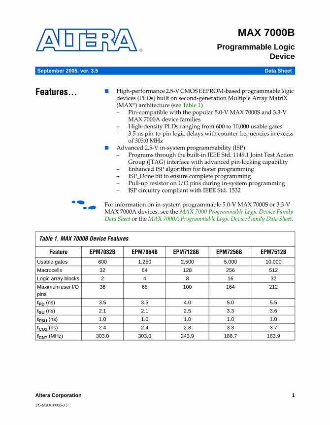
®
MAX 7000BProgrammable Logic
Device
September 2005, ver. 3.5 Data Sheet
Features... ■ High-performance 2.5-V CMOS EEPROM-based programmable logic devices (PLDs) built on second-generation Multiple Array MatriX (MAX®) architecture (see Table 1)– Pin-compatible with the popular 5.0-V MAX 7000S and 3.3-V
MAX 7000A device families– High-density PLDs ranging from 600 to 10,000 usable gates– 3.5-ns pin-to-pin logic delays with counter frequencies in excess
of 303.0 MHz■ Advanced 2.5-V in-system programmability (ISP)
– Programs through the built-in IEEE Std. 1149.1 Joint Test Action Group (JTAG) interface with advanced pin-locking capability
– Enhanced ISP algorithm for faster programming – ISP_Done bit to ensure complete programming – Pull-up resistor on I/O pins during in-system programming– ISP circuitry compliant with IEEE Std. 1532
f For information on in-system programmable 5.0-V MAX 7000S or 3.3-V MAX 7000A devices, see the MAX 7000 Programmable Logic Device Family Data Sheet or the MAX 7000A Programmable Logic Device Family Data Sheet.
Table 1. MAX 7000B Device Features
Feature EPM7032B EPM7064B EPM7128B EPM7256B EPM7512B
Usable gates 600 1,250 2,500 5,000 10,000
Macrocells 32 64 128 256 512
Logic array blocks 2 4 8 16 32
Maximum user I/O pins
36 68 100 164 212
tPD (ns) 3.5 3.5 4.0 5.0 5.5
tSU (ns) 2.1 2.1 2.5 3.3 3.6
tFSU (ns) 1.0 1.0 1.0 1.0 1.0
tCO1 (ns) 2.4 2.4 2.8 3.3 3.7
fCNT (MHz) 303.0 303.0 243.9 188.7 163.9
Altera Corporation 1
DS-MAX7000B-3.5
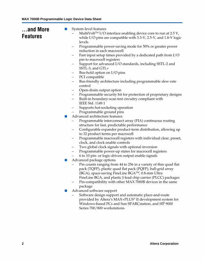
MAX 7000B Programmable Logic Device Data Sheet
...and More Features
■ System-level features– MultiVoltTM I/O interface enabling device core to run at 2.5 V,
while I/O pins are compatible with 3.3-V, 2.5-V, and 1.8-V logic levels
– Programmable power-saving mode for 50% or greater power reduction in each macrocell
– Fast input setup times provided by a dedicated path from I/O pin to macrocell registers
– Support for advanced I/O standards, including SSTL-2 and SSTL-3, and GTL+
– Bus-hold option on I/O pins– PCI compatible– Bus-friendly architecture including programmable slew-rate
control– Open-drain output option– Programmable security bit for protection of proprietary designs– Built-in boundary-scan test circuitry compliant with
IEEE Std. 1149.1– Supports hot-socketing operation– Programmable ground pins
■ Advanced architecture features– Programmable interconnect array (PIA) continuous routing
structure for fast, predictable performance– Configurable expander product-term distribution, allowing up
to 32 product terms per macrocell– Programmable macrocell registers with individual clear, preset,
clock, and clock enable controls– Two global clock signals with optional inversion– Programmable power-up states for macrocell registers– 6 to 10 pin- or logic-driven output enable signals
■ Advanced package options– Pin counts ranging from 44 to 256 in a variety of thin quad flat
pack (TQFP), plastic quad flat pack (PQFP), ball-grid array (BGA), space-saving FineLine BGATM, 0.8-mm Ultra FineLine BGA, and plastic J-lead chip carrier (PLCC) packages
– Pin-compatibility with other MAX 7000B devices in the same package
■ Advanced software support– Software design support and automatic place-and-route
provided by Altera’s MAX+PLUS® II development system for Windows-based PCs and Sun SPARCstation, and HP 9000 Series 700/800 workstations
2 Altera Corporation
MAX 7000B Programmable Logic Device Data Sheet
– Additional design entry and simulation support provided by EDIF 2 0 0 and 3 0 0 netlist files, library of parameterized modules (LPMs), Verilog HDL, VHDL, and other interfaces to popular EDA tools from manufacturers such as Cadence, Exemplar Logic, Mentor Graphics, OrCAD, Synopsys, Synplicity, and VeriBest
– Programming support with Altera’s Master Programming Unit (MPU), MasterBlasterTM serial/universal serial bus (USB) communications cable, and ByteBlasterMVTM parallel port download cable, as well as programming hardware from third-party manufacturers and any JamTM STAPL File (.jam), Jam Byte-Code File (.jbc), or Serial Vector Format File (.svf)-capable in-circuit tester
General Description
MAX 7000B devices are high-density, high-performance devices based on Altera’s second-generation MAX architecture. Fabricated with advanced CMOS technology, the EEPROM-based MAX 7000B devices operate with a 2.5-V supply voltage and provide 600 to 10,000 usable gates, ISP, pin-to-pin delays as fast as 3.5 ns, and counter speeds up to 303.0 MHz. See Table 2.
Notes:(1) Contact Altera Marketing for up-to-date information on available device speed
grades.
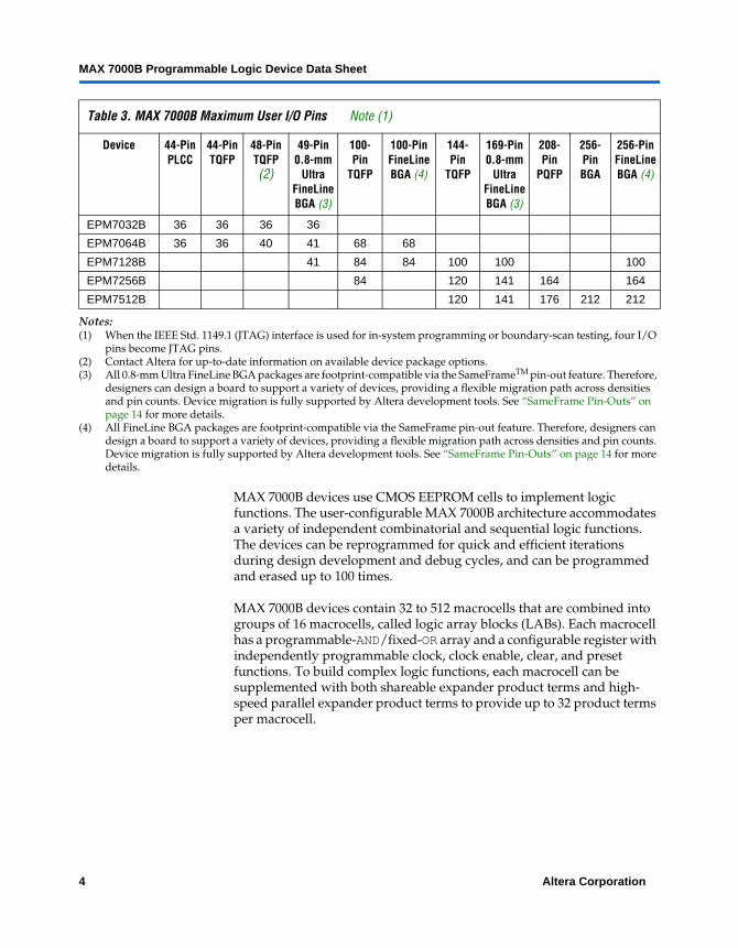
The MAX 7000B architecture supports 100% TTL emulation and high-density integration of SSI, MSI, and LSI logic functions. It easily integrates multiple devices ranging from PALs, GALs, and 22V10s to MACH and pLSI devices. MAX 7000B devices are available in a wide range of packages, including PLCC, BGA, FineLine BGA, 0.8-mm Ultra FineLine BGA, PQFP, TQFP, and TQFP packages. See Table 3.
Table 2. MAX 7000B Speed Grades Note (1)
Device Speed Grade
-3 -4 -5 -7 -10
EPM7032B v v v
EPM7064B v v v
EPM7128B v v v
EPM7256B v v v
EPM7512B v v v
Altera Corporation 3
MAX 7000B Programmable Logic Device Data Sheet
Notes:(1) When the IEEE Std. 1149.1 (JTAG) interface is used for in-system programming or boundary-scan testing, four I/O
pins become JTAG pins.(2) Contact Altera for up-to-date information on available device package options.(3) All 0.8-mm Ultra FineLine BGA packages are footprint-compatible via the SameFrameTM pin-out feature. Therefore,
designers can design a board to support a variety of devices, providing a flexible migration path across densities and pin counts. Device migration is fully supported by Altera development tools. See “SameFrame Pin-Outs” on page 14 for more details.
(4) All FineLine BGA packages are footprint-compatible via the SameFrame pin-out feature. Therefore, designers can design a board to support a variety of devices, providing a flexible migration path across densities and pin counts. Device migration is fully supported by Altera development tools. See “SameFrame Pin-Outs” on page 14 for more details.
MAX 7000B devices use CMOS EEPROM cells to implement logic functions. The user-configurable MAX 7000B architecture accommodates a variety of independent combinatorial and sequential logic functions. The devices can be reprogrammed for quick and efficient iterations during design development and debug cycles, and can be programmed and erased up to 100 times.
MAX 7000B devices contain 32 to 512 macrocells that are combined into groups of 16 macrocells, called logic array blocks (LABs). Each macrocell has a programmable-AND/fixed-OR array and a configurable register with independently programmable clock, clock enable, clear, and preset functions. To build complex logic functions, each macrocell can be supplemented with both shareable expander product terms and high-speed parallel expander product terms to provide up to 32 product terms per macrocell.
Table 3. MAX 7000B Maximum User I/O Pins Note (1)
Device 44-Pin PLCC
44-Pin TQFP
48-PinTQFP (2)
49-Pin 0.8-mm
Ultra FineLineBGA (3)
100-Pin
TQFP
100-PinFineLine BGA (4)
144-Pin
TQFP
169-Pin 0.8-mm
Ultra FineLine BGA (3)
208-Pin
PQFP
256-PinBGA
256-Pin FineLine BGA (4)
EPM7032B 36 36 36 36
EPM7064B 36 36 40 41 68 68
EPM7128B 41 84 84 100 100 100
EPM7256B 84 120 141 164 164
EPM7512B 120 141 176 212 212
4 Altera Corporation
MAX 7000B Programmable Logic Device Data Sheet
MAX 7000B devices provide programmable speed/power optimization. Speed-critical portions of a design can run at high speed/full power, while the remaining portions run at reduced speed/low power. This speed/power optimization feature enables the designer to configure one or more macrocells to operate up to 50% lower power while adding only a nominal timing delay. MAX 7000B devices also provide an option that reduces the slew rate of the output buffers, minimizing noise transients when non-speed-critical signals are switching. The output drivers of all MAX 7000B devices can be set for 3.3 V, 2.5 V, or 1.8 V and all input pins are 3.3-V, 2.5-V, and 1.8-V tolerant, allowing MAX 7000B devices to be used in mixed-voltage systems.
MAX 7000B devices are supported by Altera development systems, which are integrated packages that offer schematic, text—including VHDL, Verilog HDL, and the Altera Hardware Description Language (AHDL)—and waveform design entry, compilation and logic synthesis, simulation and timing analysis, and device programming. Altera software provides EDIF 2 0 0 and 3 0 0, LPM, VHDL, Verilog HDL, and other interfaces for additional design entry and simulation support from other industry-standard PC- and UNIX-workstation-based EDA tools. Altera software runs on Windows-based PCs, as well as Sun SPARCstation, and HP 9000 Series 700/800 workstations.
f For more information on development tools, see the MAX+PLUS II Programmable Logic Development System & Software Data Sheet and the Quartus Programmable Logic Development System & Software Data Sheet.
Functional Description
The MAX 7000B architecture includes the following elements:
■ LABs■ Macrocells■ Expander product terms (shareable and parallel)■ PIA■ I/O control blocks
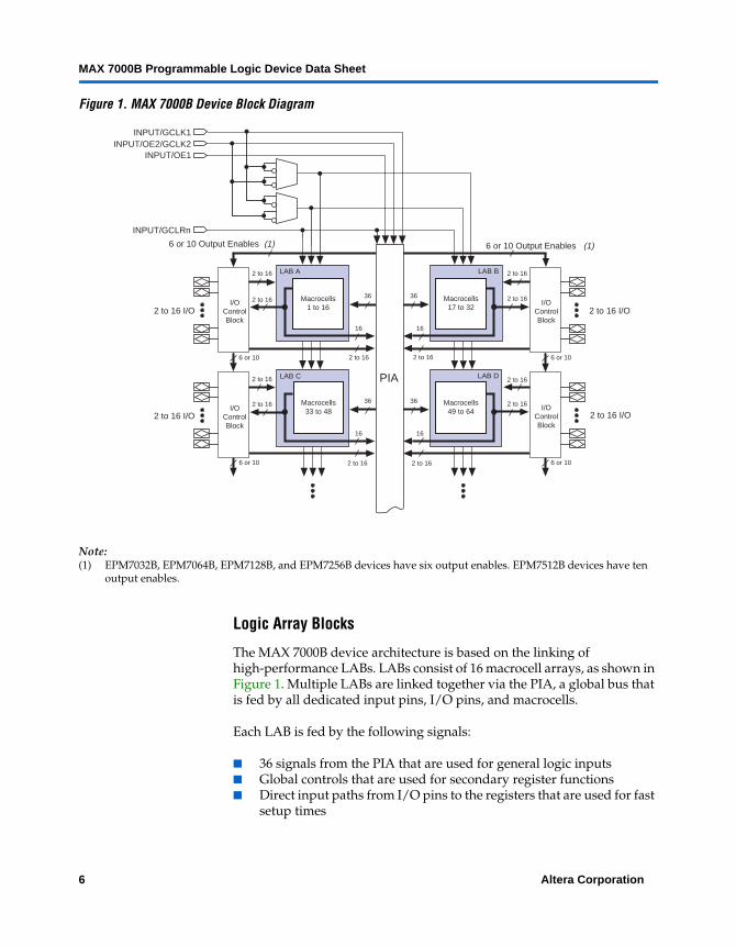
The MAX 7000B architecture includes four dedicated inputs that can be used as general-purpose inputs or as high-speed, global control signals (clock, clear, and two output enable signals) for each macrocell and I/O pin. Figure 1 shows the architecture of MAX 7000B devices.
Altera Corporation 5
MAX 7000B Programmable Logic Device Data Sheet
Figure 1. MAX 7000B Device Block Diagram
Note:(1) EPM7032B, EPM7064B, EPM7128B, and EPM7256B devices have six output enables. EPM7512B devices have ten
output enables.
Logic Array Blocks
The MAX 7000B device architecture is based on the linking of high-performance LABs. LABs consist of 16 macrocell arrays, as shown in Figure 1. Multiple LABs are linked together via the PIA, a global bus that is fed by all dedicated input pins, I/O pins, and macrocells.
Each LAB is fed by the following signals:
■ 36 signals from the PIA that are used for general logic inputs■ Global controls that are used for secondary register functions■ Direct input paths from I/O pins to the registers that are used for fast
setup times
6 or 10
6 or 10
INPUT/GCLRn
6 or 10 Output Enables (1) 6 or 10 Output Enables (1)
16
36 36
16
I/OControlBlock
LAB C LAB D
I/OControlBlock
6 or 10
16
36 36
16
I/OControlBlock
LAB A
Macrocells1 to 16
LAB B
I/OControlBlock
6 or 10
PIA
INPUT/GCLK1INPUT/OE2/GCLK2
INPUT/OE1
2 to 16 I/O
2 to 16 I/O
2 to 16 I/O
2 to 16 I/O2 to 16
2 to 16
2 to 16
2 to 16
2 to 16
2 to 16
2 to 16
2 to 16
2 to 162 to 16
2 to 162 to 16
Macrocells17 to 32
Macrocells33 to 48
Macrocells49 to 64
6 Altera Corporation
MAX 7000B Programmable Logic Device Data Sheet
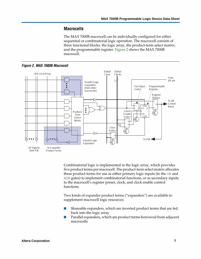
Macrocells
The MAX 7000B macrocell can be individually configured for either sequential or combinatorial logic operation. The macrocell consists of three functional blocks: the logic array, the product-term select matrix, and the programmable register. Figure 2 shows the MAX 7000B macrocell.
Figure 2. MAX 7000B Macrocell
Combinatorial logic is implemented in the logic array, which provides five product terms per macrocell. The product-term select matrix allocates these product terms for use as either primary logic inputs (to the OR and XOR gates) to implement combinatorial functions, or as secondary inputs to the macrocell’s register preset, clock, and clock enable control functions.
Two kinds of expander product terms (“expanders”) are available to supplement macrocell logic resources:
■ Shareable expanders, which are inverted product terms that are fed back into the logic array
■ Parallel expanders, which are product terms borrowed from adjacent macrocells
Product-Term Select Matrix
36 Signalsfrom PIA
16 Expander Product Terms
LAB Local Array
Parallel Logic Expanders(from other macrocells)
Shared Logic Expanders
Clear Select
Global Clear
Global Clocks
Clock/ Enable Select
2
PRN
CLRN
D/T Q
ENA
Register Bypass
To I/O Control Block
From I/O pin
To PIA
ProgrammableRegister
Fast InputSelect
VCC
Altera Corporation 7
MAX 7000B Programmable Logic Device Data Sheet
The Altera development system automatically optimizes product-term allocation according to the logic requirements of the design.
For registered functions, each macrocell flipflop can be individually programmed to implement D, T, JK, or SR operation with programmable clock control. The flipflop can be bypassed for combinatorial operation. During design entry, the designer specifies the desired flipflop type; the MAX+PLUS II software then selects the most efficient flipflop operation for each registered function to optimize resource utilization.
Each programmable register can be clocked in three different modes:
■ Global clock signal. This mode achieves the fastest clock-to-output performance.
■ Global clock signal enabled by an active-high clock enable. A clock enable is generated by a product term. This mode provides an enable on each flipflop while still achieving the fast clock-to-output performance of the global clock.
■ Array clock implemented with a product term. In this mode, the flipflop can be clocked by signals from buried macrocells or I/O pins.
Two global clock signals are available in MAX 7000B devices. As shown in Figure 1, these global clock signals can be the true or the complement of either of the global clock pins, GCLK1 or GCLK2.
Each register also supports asynchronous preset and clear functions. As shown in Figure 2, the product-term select matrix allocates product terms to control these operations. Although the product-term-driven preset and clear from the register are active high, active-low control can be obtained by inverting the signal within the logic array. In addition, each register clear function can be individually driven by the active-low dedicated global clear pin (GCLRn). Upon power-up, each register in a MAX 7000B device may be set to either a high or low state. This power-up state is specified at design entry.
All MAX 7000B I/O pins have a fast input path to a macrocell register. This dedicated path allows a signal to bypass the PIA and combinatorial logic and be clocked to an input D flipflop with an extremely fast input setup time. The input path from the I/O pin to the register has a programmable delay element that can be selected to either guarantee zero hold time or to get the fastest possible set-up time (as fast as 1.0 ns).
8 Altera Corporation
MAX 7000B Programmable Logic Device Data Sheet
Expander Product Terms
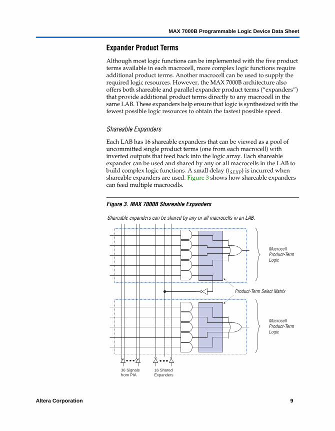
Although most logic functions can be implemented with the five product terms available in each macrocell, more complex logic functions require additional product terms. Another macrocell can be used to supply the required logic resources. However, the MAX 7000B architecture also offers both shareable and parallel expander product terms (“expanders”) that provide additional product terms directly to any macrocell in the same LAB. These expanders help ensure that logic is synthesized with the fewest possible logic resources to obtain the fastest possible speed.
Shareable Expanders
Each LAB has 16 shareable expanders that can be viewed as a pool of uncommitted single product terms (one from each macrocell) with inverted outputs that feed back into the logic array. Each shareable expander can be used and shared by any or all macrocells in the LAB to build complex logic functions. A small delay (tSEXP) is incurred when shareable expanders are used. Figure 3 shows how shareable expanders can feed multiple macrocells.
Figure 3. MAX 7000B Shareable Expanders
Shareable expanders can be shared by any or all macrocells in an LAB.
MacrocellProduct-TermLogic
Product-Term Select Matrix
MacrocellProduct-TermLogic
36 Signalsfrom PIA
16 SharedExpanders
Altera Corporation 9
MAX 7000B Programmable Logic Device Data Sheet
Parallel Expanders
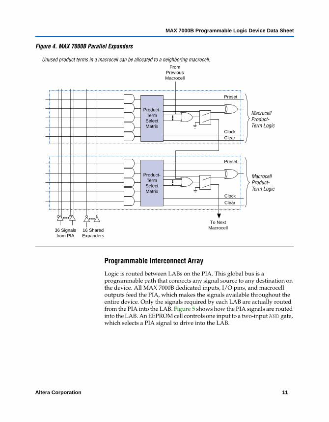
Parallel expanders are unused product terms that can be allocated to a neighboring macrocell to implement fast, complex logic functions. Parallel expanders allow up to 20 product terms to directly feed the macrocell OR logic, with five product terms provided by the macrocell and 15 parallel expanders provided by neighboring macrocells in the LAB.
The Altera Compiler can automatically allocate up to three sets of up to five parallel expanders to the macrocells that require additional product terms. Each set of five parallel expanders incurs a small, incremental timing delay (tPEXP). For example, if a macrocell requires 14 product terms, the Compiler uses the five dedicated product terms within the macrocell and allocates two sets of parallel expanders; the first set includes five product terms and the second set includes four product terms, increasing the total delay by 2 × tPEXP.
Two groups of eight macrocells within each LAB (e.g., macrocells 1 through 8, and 9 through 16) form two chains to lend or borrow parallel expanders. A macrocell borrows parallel expanders from lower-numbered macrocells. For example, macrocell 8 can borrow parallel expanders from macrocell 7, from macrocells 7 and 6, or from macrocells 7, 6, and 5. Within each group of eight, the lowest-numbered macrocell can only lend parallel expanders and the highest-numbered macrocell can only borrow them. Figure 4 shows how parallel expanders can be borrowed from a neighboring macrocell.
10 Altera Corporation
MAX 7000B Programmable Logic Device Data Sheet
Figure 4. MAX 7000B Parallel Expanders
Unused product terms in a macrocell can be allocated to a neighboring macrocell.
Programmable Interconnect Array
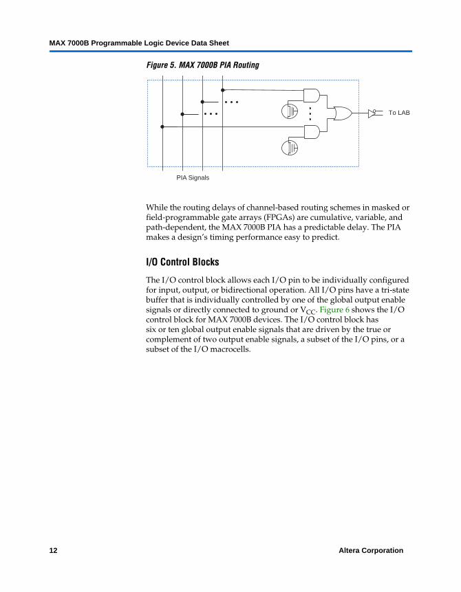
Logic is routed between LABs on the PIA. This global bus is a programmable path that connects any signal source to any destination on the device. All MAX 7000B dedicated inputs, I/O pins, and macrocell outputs feed the PIA, which makes the signals available throughout the entire device. Only the signals required by each LAB are actually routed from the PIA into the LAB. Figure 5 shows how the PIA signals are routed into the LAB. An EEPROM cell controls one input to a two-input AND gate, which selects a PIA signal to drive into the LAB.
Preset
ClockClear
Product-TermSelectMatrix
Preset
Clock
Clear
Product-TermSelectMatrix
MacrocellProduct-Term Logic
FromPreviousMacrocell
To NextMacrocell
MacrocellProduct-Term Logic
36 Signalsfrom PIA
16 SharedExpanders
Altera Corporation 11
MAX 7000B Programmable Logic Device Data Sheet
Figure 5. MAX 7000B PIA Routing
While the routing delays of channel-based routing schemes in masked or field-programmable gate arrays (FPGAs) are cumulative, variable, and path-dependent, the MAX 7000B PIA has a predictable delay. The PIA makes a design’s timing performance easy to predict.
I/O Control Blocks
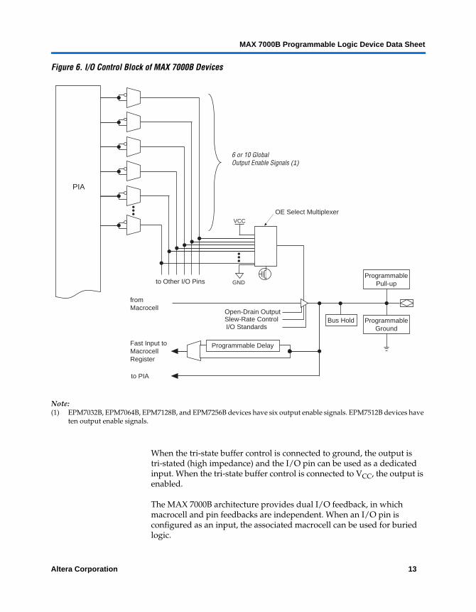
The I/O control block allows each I/O pin to be individually configured for input, output, or bidirectional operation. All I/O pins have a tri-state buffer that is individually controlled by one of the global output enable signals or directly connected to ground or VCC. Figure 6 shows the I/O control block for MAX 7000B devices. The I/O control block has six or ten global output enable signals that are driven by the true or complement of two output enable signals, a subset of the I/O pins, or a subset of the I/O macrocells.
To LAB
PIA Signals
12 Altera Corporation
MAX 7000B Programmable Logic Device Data Sheet
Figure 6. I/O Control Block of MAX 7000B Devices
Note:(1) EPM7032B, EPM7064B, EPM7128B, and EPM7256B devices have six output enable signals. EPM7512B devices have
ten output enable signals.
When the tri-state buffer control is connected to ground, the output is tri-stated (high impedance) and the I/O pin can be used as a dedicated input. When the tri-state buffer control is connected to VCC, the output is enabled.
The MAX 7000B architecture provides dual I/O feedback, in which macrocell and pin feedbacks are independent. When an I/O pin is configured as an input, the associated macrocell can be used for buried logic.
fromMacrocell
Fast Input toMacrocellRegister
Slew-Rate ControlI/O Standards
to PIA
to Other I/O Pins
6 or 10 GlobalOutput Enable Signals (1)
PIA
VCC
Open-Drain Output
OE Select Multiplexer
GND
Programmable Delay
Bus Hold ProgrammableGround
ProgrammablePull-up
Altera Corporation 13
MAX 7000B Programmable Logic Device Data Sheet
14 Altera Corporation
SameFrame Pin-Outs
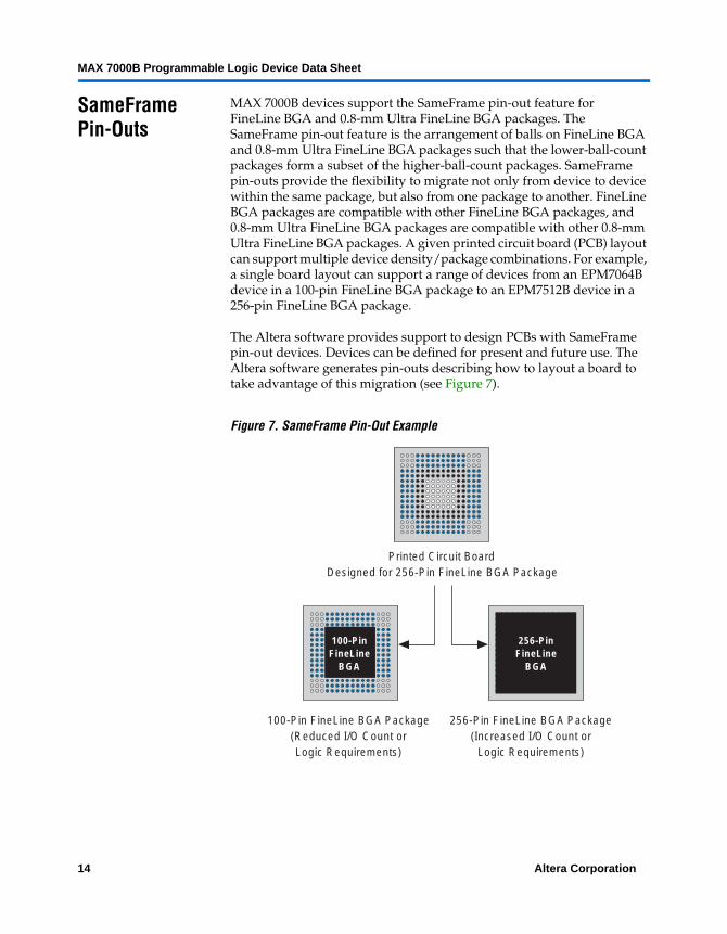
MAX 7000B devices support the SameFrame pin-out feature for FineLine BGA and 0.8-mm Ultra FineLine BGA packages. The SameFrame pin-out feature is the arrangement of balls on FineLine BGA and 0.8-mm Ultra FineLine BGA packages such that the lower-ball-count packages form a subset of the higher-ball-count packages. SameFrame pin-outs provide the flexibility to migrate not only from device to device within the same package, but also from one package to another. FineLine BGA packages are compatible with other FineLine BGA packages, and 0.8-mm Ultra FineLine BGA packages are compatible with other 0.8-mm Ultra FineLine BGA packages. A given printed circuit board (PCB) layout can support multiple device density/package combinations. For example, a single board layout can support a range of devices from an EPM7064B device in a 100-pin FineLine BGA package to an EPM7512B device in a 256-pin FineLine BGA package.
The Altera software provides support to design PCBs with SameFrame pin-out devices. Devices can be defined for present and future use. The Altera software generates pin-outs describing how to layout a board to take advantage of this migration (see Figure 7).
Figure 7. SameFrame Pin-Out Example
Designed for 256-Pin FineLine BGA PackagePrinted Circuit Board
100-Pin FineLine BGA Package(Reduced I/O Count orLogic Requirements)
256-Pin FineLine BGA Package(Increased I/O Count or
Logic Requirements)
100-PinFineLine
BGA
256-PinFineLine
BGA
MAX 7000B Programmable Logic Device Data Sheet
In-System Programma-bility (ISP)
MAX 7000B devices can be programmed in-system via an industry-standard 4-pin IEEE Std. 1149.1 (JTAG) interface. ISP offers quick, efficient iterations during design development and debugging cycles. The MAX 7000B architecture internally generates the high programming voltages required to program EEPROM cells, allowing in-system programming with only a single 2.5-V power supply. During in-system programming, the I/O pins are tri-stated and weakly pulled-up to eliminate board conflicts. The pull-up value is nominally 50 k¾.
MAX 7000B devices have an enhanced ISP algorithm for faster programming. These devices also offer an ISP_Done bit that provides safe operation when in-system programming is interrupted. This ISP_Done bit, which is the last bit programmed, prevents all I/O pins from driving until the bit is programmed.
ISP simplifies the manufacturing flow by allowing devices to be mounted on a PCB with standard pick-and-place equipment before they are programmed. MAX 7000B devices can be programmed by downloading the information via in-circuit testers, embedded processors, the Altera MasterBlaster communications cable, and the ByteBlasterMV parallel port download cable. Programming the devices after they are placed on the board eliminates lead damage on high-pin-count packages (e.g., QFP packages) due to device handling. MAX 7000B devices can be reprogrammed after a system has already shipped to the field. For example, product upgrades can be performed in the field via software or modem.
In-system programming can be accomplished with either an adaptive or constant algorithm. An adaptive algorithm reads information from the unit and adapts subsequent programming steps to achieve the fastest possible programming time for that unit. A constant algorithm uses a pre-defined (non-adaptive) programming sequence that does not take advantage of adaptive algorithm programming time improvements. Some in-circuit testers cannot program using an adaptive algorithm. Therefore, a constant algorithm must be used. MAX 7000B devices can be programmed with either an adaptive or constant (non-adaptive) algorithm.
The Jam Standard Test and Programming Language (STAPL), JEDEC standard JESD-71, can be used to program MAX 7000B devices with in-circuit testers, PCs, or embedded processors.
f For more information on using the Jam language, see Application Note 88 (Using the Jam Language for ISP & ICR via an Embedded Processor) and Application Note 122 (Using STAPL for ISP & ICR via an Embedded Processor).
The ISP circuitry in MAX 7000B devices is compliant with the IEEE Std. 1532 specification. The IEEE Std. 1532 is a standard developed to allow concurrent ISP between multiple PLD vendors.
Altera Corporation 15
MAX 7000B Programmable Logic Device Data Sheet
Programming Sequence
During in-system programming, instructions, addresses, and data are shifted into the MAX 7000B device through the TDI input pin. Data is shifted out through the TDO output pin and compared against the expected data.
Programming a pattern into the device requires the following six ISP stages. A stand-alone verification of a programmed pattern involves only stages 1, 2, 5, and 6.
1. Enter ISP. The enter ISP stage ensures that the I/O pins transition smoothly from user mode to ISP mode. The enter ISP stage requires 1 ms.
2. Check ID. Before any program or verify process, the silicon ID is checked. The time required to read this silicon ID is relatively small compared to the overall programming time.
3. Bulk Erase. Erasing the device in-system involves shifting in the instructions to erase the device and applying one erase pulse of 100 ms.
4. Program. Programming the device in-system involves shifting in the address and data and then applying the programming pulse to program the EEPROM cells. This process is repeated for each EEPROM address.
5. Verify. Verifying an Altera device in-system involves shifting in addresses, applying the read pulse to verify the EEPROM cells, and shifting out the data for comparison. This process is repeated for each EEPROM address.
6. Exit ISP. An exit ISP stage ensures that the I/O pins transition smoothly from ISP mode to user mode. The exit ISP stage requires 1 ms.
Programming Times
The time required to implement each of the six programming stages can be broken into the following two elements:
■ A pulse time to erase, program, or read the EEPROM cells.■ A shifting time based on the test clock (TCK) frequency and the
number of TCK cycles to shift instructions, address, and data into the device.
16 Altera Corporation
MAX 7000B Programmable Logic Device Data Sheet
By combining the pulse and shift times for each of the programming stages, the program or verify time can be derived as a function of the TCK frequency, the number of devices, and specific target device(s). Because different ISP-capable devices have a different number of EEPROM cells, both the total fixed and total variable times are unique for a single device.
Programming a Single MAX 7000B Device
The time required to program a single MAX 7000B device in-system can be calculated from the following formula:
where: tPROG = Programming timetPPULSE = Sum of the fixed times to erase, program, and
verify the EEPROM cellsCyclePTCK = Number of TCK cycles to program a devicefTCK = TCK frequency
The ISP times for a stand-alone verification of a single MAX 7000B device can be calculated from the following formula:
where: tVER = Verify timetVPULSE = Sum of the fixed times to verify the EEPROM cellsCycleVTCK = Number of TCK cycles to verify a device
tPROG tPPULSE
CyclePTCKfTCK
--------------------------------+=
tVER tVPULSE
CycleVTCKfTCK
--------------------------------+=
Altera Corporation 17
MAX 7000B Programmable Logic Device Data Sheet
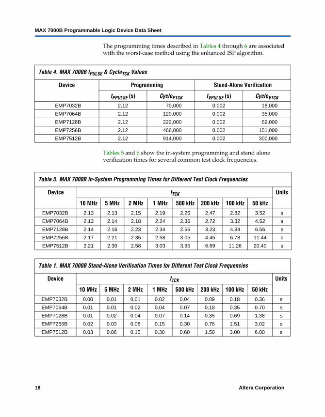
The programming times described in Tables 4 through 6 are associated with the worst-case method using the enhanced ISP algorithm.
Tables 5 and 6 show the in-system programming and stand alone verification times for several common test clock frequencies.
Table 4. MAX 7000B tPULSE & CycleTCK Values
Device Programming Stand-Alone Verification
tPPULSE (s) CyclePTCK tVPULSE (s) CycleVTCK
EMP7032B 2.12 70,000 0.002 18,000
EMP7064B 2.12 120,000 0.002 35,000
EMP7128B 2.12 222,000 0.002 69,000
EMP7256B 2.12 466,000 0.002 151,000
EMP7512B 2.12 914,000 0.002 300,000
Table 5. MAX 7000B In-System Programming Times for Different Test Clock Frequencies
Device fTCK Units
10 MHz 5 MHz 2 MHz 1 MHz 500 kHz 200 kHz 100 kHz 50 kHz
EMP7032B 2.13 2.13 2.15 2.19 2.26 2.47 2.82 3.52 s
EMP7064B 2.13 2.14 2.18 2.24 2.36 2.72 3.32 4.52 s
EMP7128B 2.14 2.16 2.23 2.34 2.56 3.23 4.34 6.56 s
EMP7256B 2.17 2.21 2.35 2.58 3.05 4.45 6.78 11.44 s
EMP7512B 2.21 2.30 2.58 3.03 3.95 6.69 11.26 20.40 s
Table 1. MAX 7000B Stand-Alone Verification Times for Different Test Clock Frequencies
Device fTCK Units
10 MHz 5 MHz 2 MHz 1 MHz 500 kHz 200 kHz 100 kHz 50 kHz
EMP7032B 0.00 0.01 0.01 0.02 0.04 0.09 0.18 0.36 s
EMP7064B 0.01 0.01 0.02 0.04 0.07 0.18 0.35 0.70 s
EMP7128B 0.01 0.02 0.04 0.07 0.14 0.35 0.69 1.38 s
EMP7256B 0.02 0.03 0.08 0.15 0.30 0.76 1.51 3.02 s
EMP7512B 0.03 0.06 0.15 0.30 0.60 1.50 3.00 6.00 s
18 Altera Corporation
MAX 7000B Programmable Logic Device Data Sheet
Programming with External Hardware
MAX 7000B devices can be programmed on Windows-based PCs with an Altera Logic Programmer card, the Master Programming Unit (MPU), and the appropriate device adapter. The MPU performs continuity checking to ensure adequate electrical contact between the adapter and the device.
f For more information, see the Altera Programming Hardware Data Sheet.
The Altera software can use text- or waveform-format test vectors created with the Altera Text Editor or Waveform Editor to test the programmed device. For added design verification, designers can perform functional testing to compare the functional device behavior with the results of simulation.
Data I/O, BP Microsystems, and other programming hardware manufacturers provide programming support for Altera devices. For more information, see Programming Hardware Manufacturers.
IEEE Std. 1149.1 (JTAG) Boundary-Scan Support
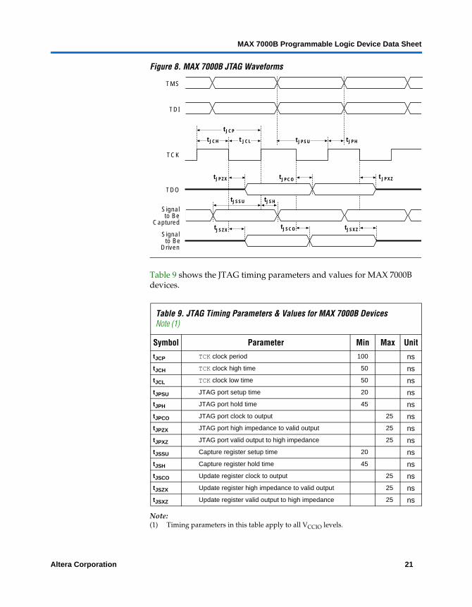
MAX 7000B devices include the JTAG boundary-scan test circuitry defined by IEEE Std. 1149.1. Table 6 describes the JTAG instructions supported by MAX 7000B devices. The pin-out tables starting on page 59 of this data sheet show the location of the JTAG control pins for each device. If the JTAG interface is not required, the JTAG pins are available as user I/O pins.
Table 6. MAX 7000B JTAG Instructions
JTAG Instruction Description
SAMPLE/PRELOAD Allows a snapshot of signals at the device pins to be captured and examined during normal device operation, and permits an initial data pattern output at the device pins.
EXTEST Allows the external circuitry and board-level interconnections to be tested by forcing a test pattern at the output pins and capturing test results at the input pins.
BYPASS Places the 1-bit bypass register between the TDI and TDO pins, which allows the boundary-scan test data to pass synchronously through a selected device to adjacent devices during normal operation.
CLAMP Allows the values in the boundary-scan register to determine pin states while placing the 1-bit bypass register between the TDI and TDO pins.
IDCODE Selects the IDCODE register and places it between the TDI and TDO pins, allowing the IDCODE to be serially shifted out of TDO.
USERCODE Selects the 32-bit USERCODE register and places it between the TDI and TDO pins, allowing the USERCODE value to be shifted out of TDO.
ISP Instructions These instructions are used when programming MAX 7000B devices via the JTAG ports with the MasterBlaster or ByteBlasterMV download cable, or using a Jam File (.jam), Jam Byte-Code File (.jbc), or Serial Vector Format File (.svf) via an embedded processor or test equipment.
Altera Corporation 19
MAX 7000B Programmable Logic Device Data Sheet
The instruction register length of MAX 7000B devices is ten bits. The MAX 7000B USERCODE register length is 32 bits. Tables 7 and 8 show the boundary-scan register length and device IDCODE information for MAX 7000B devices.
Notes:(1) The most significant bit (MSB) is on the left.(2) The least significant bit (LSB) for all JTAG IDCODEs is 1.
f See Application Note 39 (IEEE 1149.1 (JTAG) Boundary-Scan Testing in Altera Devices) for more information on JTAG boundary-scan testing.
Figure 8 shows the timing information for the JTAG signals.
Table 7. MAX 7000B Boundary-Scan Register Length
Device Boundary-Scan Register Length
EPM7032B 96
EPM7064B 192
EPM7128B 288
EPM7256B 480
EPM7512B 624
Table 8. 32-Bit MAX 7000B Device IDCODE Note (1)
Device IDCODE (32 Bits)
Version (4 Bits)
Part Number (16 Bits) Manufacturer’sIdentity (11 Bits)
1 (1 Bit) (2)
EPM7032B 0010 0111 0000 0011 0010 00001101110 1
EPM7064B 0010 0111 0000 0110 0100 00001101110 1
EPM7128B 0010 0111 0001 0010 1000 00001101110 1
EPM7256B 0010 0111 0010 0101 0110 00001101110 1
EPM7512B 0010 0111 0101 0001 0010 00001101110 1
20 Altera Corporation
MAX 7000B Programmable Logic Device Data Sheet
Figure 8. MAX 7000B JTAG Waveforms
Table 9 shows the JTAG timing parameters and values for MAX 7000B devices.
Note:(1) Timing parameters in this table apply to all VCCIO levels.
Table 9. JTAG Timing Parameters & Values for MAX 7000B Devices Note (1)
Symbol Parameter Min Max UnittJCP TCK clock period 100 ns
tJCH TCK clock high time 50 ns
tJCL TCK clock low time 50 ns
tJPSU JTAG port setup time 20 ns
tJPH JTAG port hold time 45 ns
tJPCO JTAG port clock to output 25 ns
tJPZX JTAG port high impedance to valid output 25 ns
tJPXZ JTAG port valid output to high impedance 25 ns
tJSSU Capture register setup time 20 ns
tJSH Capture register hold time 45 ns
tJSCO Update register clock to output 25 ns
tJSZX Update register high impedance to valid output 25 ns
tJSXZ Update register valid output to high impedance 25 ns
TDO
TCK
tJPZX tJPCO
tJPH
t JPXZ
tJCP
tJPSU t JCL tJCH
TDI
TMS
Signalto Be
Captured
Signalto Be
Driven
tJSZX
tJSSU tJSH
tJSCO tJSXZ
Altera Corporation 21
MAX 7000B Programmable Logic Device Data Sheet
Programmable Speed/Power Control
MAX 7000B devices offer a power-saving mode that supports low-power operation across user-defined signal paths or the entire device. This feature allows total power dissipation to be reduced by 50% or more, because most logic applications require only a small fraction of all gates to operate at maximum frequency.
The designer can program each individual macrocell in a MAX 7000B device for either high-speed or low-power operation. As a result, speed-critical paths in the design can run at high speed, while the remaining paths can operate at reduced power. Macrocells that run at low power incur a nominal timing delay adder (tLPA) for the tLAD, tLAC, tIC, tACL, tCPPW, tEN, and tSEXP parameters.
Output Configuration
MAX 7000B device outputs can be programmed to meet a variety of system-level requirements.
MultiVolt I/O Interface
The MAX 7000B device architecture supports the MultiVolt I/O interface feature, which allows MAX 7000B devices to connect to systems with differing supply voltages. MAX 7000B devices in all packages can be set for 3.3-V, 2.5-V, or 1.8-V pin operation. These devices have one set of VCC pins for internal operation and input buffers (VCCINT), and another set for I/O output drivers (VCCIO).
The VCCIO pins can be connected to either a 3.3-V, 2.5-V, or 1.8-V power supply, depending on the output requirements. When the VCCIO pins are connected to a 1.8-V power supply, the output levels are compatible with 1.8-V systems. When the VCCIO pins are connected to a 2.5-V power supply, the output levels are compatible with 2.5-V systems. When the VCCIO pins are connected to a 3.3-V power supply, the output high is at 3.3 V and is therefore compatible with 3.3-V or 5.0-V systems. Devices operating with VCCIO levels of 2.5 V or 1.8 V incur a nominal timing delay adder.
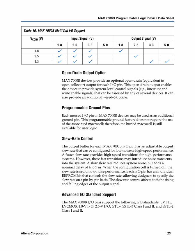
Table 10 describes the MAX 7000B MultiVolt I/O support.
22 Altera Corporation
MAX 7000B Programmable Logic Device Data Sheet
Open-Drain Output Option
MAX 7000B devices provide an optional open-drain (equivalent to open-collector) output for each I/O pin. This open-drain output enables the device to provide system-level control signals (e.g., interrupt and write enable signals) that can be asserted by any of several devices. It can also provide an additional wired-OR plane.
Programmable Ground Pins
Each unused I/O pin on MAX 7000B devices may be used as an additional ground pin. This programmable ground feature does not require the use of the associated macrocell; therefore, the buried macrocell is still available for user logic.
Slew-Rate Control
The output buffer for each MAX 7000B I/O pin has an adjustable output slew rate that can be configured for low-noise or high-speed performance. A faster slew rate provides high-speed transitions for high-performance systems. However, these fast transitions may introduce noise transients into the system. A slow slew rate reduces system noise, but adds a nominal delay of 4 to 5 ns. When the configuration cell is turned off, the slew rate is set for low-noise performance. Each I/O pin has an individual EEPROM bit that controls the slew rate, allowing designers to specify the slew rate on a pin-by-pin basis. The slew rate control affects both the rising and falling edges of the output signal.
Advanced I/O Standard Support
The MAX 7000B I/O pins support the following I/O standards: LVTTL, LVCMOS, 1.8-V I/O, 2.5-V I/O, GTL+, SSTL-3 Class I and II, and SSTL-2 Class I and II.
Table 10. MAX 7000B MultiVolt I/O Support
VCCIO (V) Input Signal (V) Output Signal (V)
1.8 2.5 3.3 5.0 1.8 2.5 3.3 5.0
1.8 v v v v
2.5 v v v v
3.3 v v v v v
Altera Corporation 23
MAX 7000B Programmable Logic Device Data Sheet
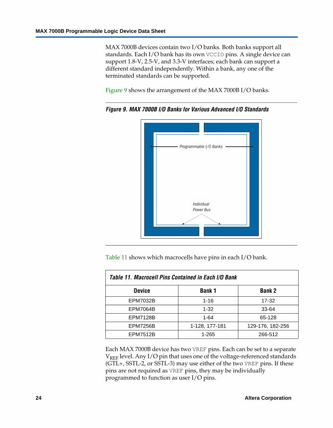
MAX 7000B devices contain two I/O banks. Both banks support all standards. Each I/O bank has its own VCCIO pins. A single device can support 1.8-V, 2.5-V, and 3.3-V interfaces; each bank can support a different standard independently. Within a bank, any one of the terminated standards can be supported.
Figure 9 shows the arrangement of the MAX 7000B I/O banks.
Figure 9. MAX 7000B I/O Banks for Various Advanced I/O Standards
Table 11 shows which macrocells have pins in each I/O bank.
Each MAX 7000B device has two VREF pins. Each can be set to a separate VREF level. Any I/O pin that uses one of the voltage-referenced standards (GTL+, SSTL-2, or SSTL-3) may use either of the two VREF pins. If these pins are not required as VREF pins, they may be individually programmed to function as user I/O pins.
Table 11. Macrocell Pins Contained in Each I/O Bank
Device Bank 1 Bank 2
EPM7032B 1-16 17-32
EPM7064B 1-32 33-64
EPM7128B 1-64 65-128
EPM7256B 1-128, 177-181 129-176, 182-256
EPM7512B 1-265 266-512
IndividualPower Bus
Programmable I/O Banks
24 Altera Corporation
MAX 7000B Programmable Logic Device Data Sheet
Programmable Pull-Up Resistor
Each MAX 7000B device I/O pin provides an optional programmable pull-up resistor during user mode. When this feature is enabled for an I/O pin, the pull-up resistor (typically 50 k¾) weakly holds the output to VCCIO level.
Bus Hold
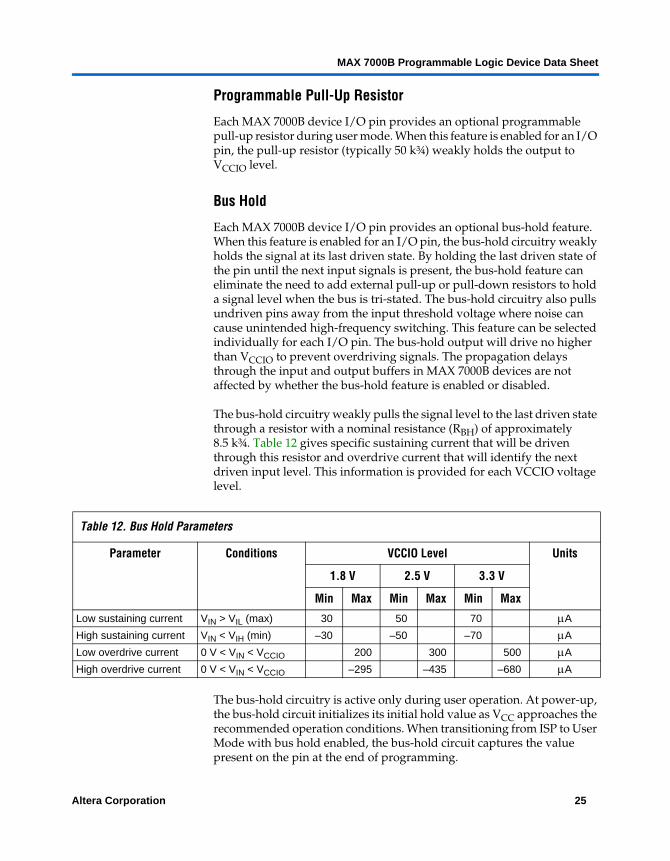
Each MAX 7000B device I/O pin provides an optional bus-hold feature. When this feature is enabled for an I/O pin, the bus-hold circuitry weakly holds the signal at its last driven state. By holding the last driven state of the pin until the next input signals is present, the bus-hold feature can eliminate the need to add external pull-up or pull-down resistors to hold a signal level when the bus is tri-stated. The bus-hold circuitry also pulls undriven pins away from the input threshold voltage where noise can cause unintended high-frequency switching. This feature can be selected individually for each I/O pin. The bus-hold output will drive no higher than VCCIO to prevent overdriving signals. The propagation delays through the input and output buffers in MAX 7000B devices are not affected by whether the bus-hold feature is enabled or disabled.
The bus-hold circuitry weakly pulls the signal level to the last driven state through a resistor with a nominal resistance (RBH) of approximately 8.5 k¾. Table 12 gives specific sustaining current that will be driven through this resistor and overdrive current that will identify the next driven input level. This information is provided for each VCCIO voltage level.
The bus-hold circuitry is active only during user operation. At power-up, the bus-hold circuit initializes its initial hold value as VCC approaches the recommended operation conditions. When transitioning from ISP to User Mode with bus hold enabled, the bus-hold circuit captures the value present on the pin at the end of programming.
Table 12. Bus Hold Parameters
Parameter Conditions VCCIO Level Units
1.8 V 2.5 V 3.3 V
Min Max Min Max Min Max
Low sustaining current VIN > VIL (max) 30 50 70 μA
High sustaining current VIN < VIH (min) –30 –50 –70 μA
Low overdrive current 0 V < VIN < VCCIO 200 300 500 μA
High overdrive current 0 V < VIN < VCCIO –295 –435 –680 μA
Altera Corporation 25
MAX 7000B Programmable Logic Device Data Sheet
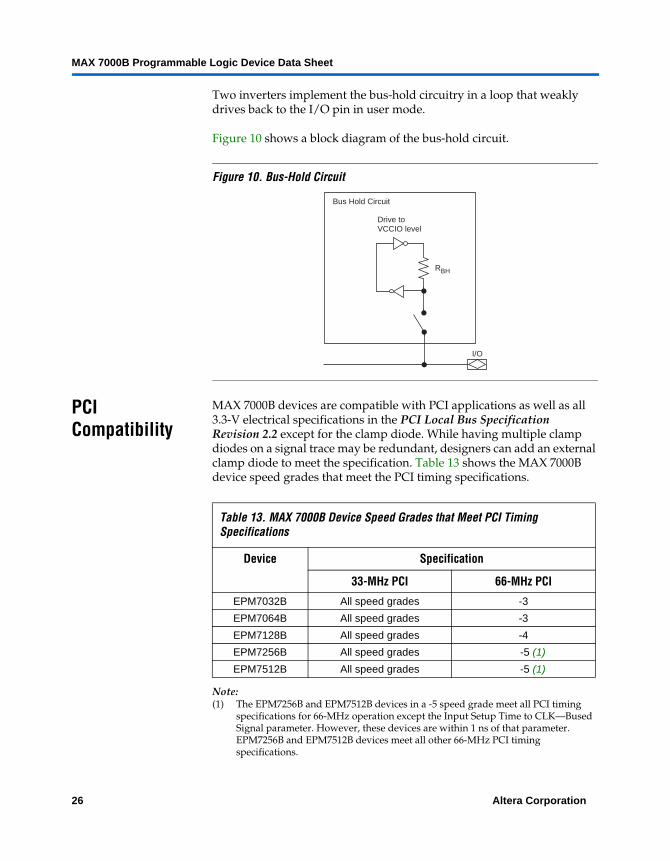
Two inverters implement the bus-hold circuitry in a loop that weakly drives back to the I/O pin in user mode.
Figure 10 shows a block diagram of the bus-hold circuit.
Figure 10. Bus-Hold Circuit
PCI Compatibility
MAX 7000B devices are compatible with PCI applications as well as all 3.3-V electrical specifications in the PCI Local Bus Specification Revision 2.2 except for the clamp diode. While having multiple clamp diodes on a signal trace may be redundant, designers can add an external clamp diode to meet the specification. Table 13 shows the MAX 7000B device speed grades that meet the PCI timing specifications.
Note:(1) The EPM7256B and EPM7512B devices in a -5 speed grade meet all PCI timing
specifications for 66-MHz operation except the Input Setup Time to CLK—Bused Signal parameter. However, these devices are within 1 ns of that parameter. EPM7256B and EPM7512B devices meet all other 66-MHz PCI timing specifications.
I/O
RBH
Bus Hold Circuit
Drive to VCCIO level
Table 13. MAX 7000B Device Speed Grades that Meet PCI Timing Specifications
Device Specification
33-MHz PCI 66-MHz PCI
EPM7032B All speed grades -3
EPM7064B All speed grades -3
EPM7128B All speed grades -4
EPM7256B All speed grades -5 (1)
EPM7512B All speed grades -5 (1)
26 Altera Corporation
MAX 7000B Programmable Logic Device Data Sheet
Power Sequencing & Hot-Socketing
Because MAX 7000B devices can be used in a mixed-voltage environment, they have been designed specifically to tolerate any possible power-up sequence. The VCCIO and VCCINT power planes can be powered in any order.
Signals can be driven into MAX 7000B devices before and during power-up (and power-down) without damaging the device. Additionally, MAX 7000B devices do not drive out during power-up. Once operating conditions are reached, MAX 7000B devices operate as specified by the user.
MAX 7000B device I/O pins will not source or sink more than 300 µA of DC current during power-up. All pins can be driven up to 4.1 V during hot-socketing.
Design Security All MAX 7000B devices contain a programmable security bit that controls access to the data programmed into the device. When this bit is programmed, a design implemented in the device cannot be copied or retrieved. This feature provides a high level of design security, because programmed data within EEPROM cells is invisible. The security bit that controls this function, as well as all other programmed data, is reset only when the device is reprogrammed.
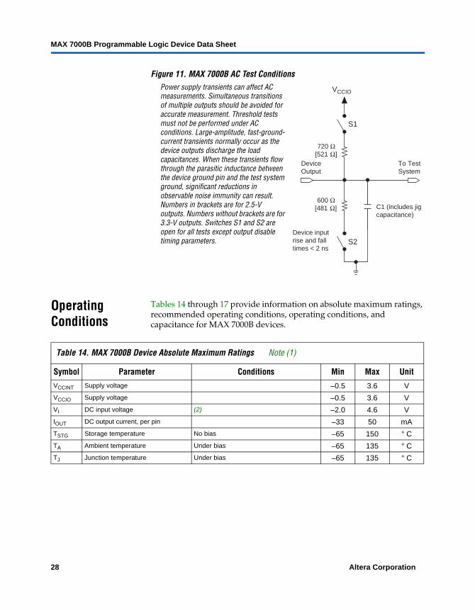
Generic Testing MAX 7000B devices are fully functionally tested. Complete testing of each programmable EEPROM bit and all internal logic elements ensures 100% programming yield. AC test measurements are taken under conditions equivalent to those shown in Figure 11. Test patterns can be used and then erased during early stages of the production flow.
Altera Corporation 27
MAX 7000B Programmable Logic Device Data Sheet
Figure 11. MAX 7000B AC Test Conditions
Operating Conditions
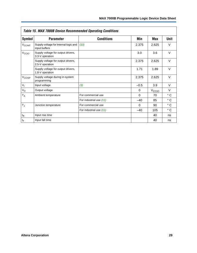
Tables 14 through 17 provide information on absolute maximum ratings, recommended operating conditions, operating conditions, and capacitance for MAX 7000B devices.
To TestSystem
C1 (includes jigcapacitance)
Device inputrise and falltimes < 2 ns
DeviceOutput
720 Ω[521 Ω]
600 Ω[481 Ω]
VCCIO
S2
S1
Power supply transients can affect ACmeasurements. Simultaneous transitionsof multiple outputs should be avoided foraccurate measurement. Threshold testsmust not be performed under ACconditions. Large-amplitude, fast-ground-current transients normally occur as the device outputs discharge the load capacitances. When these transients flow through the parasitic inductance between the device ground pin and the test system ground, significant reductions in observable noise immunity can result. Numbers in brackets are for 2.5-V outputs. Numbers without brackets are for 3.3-V outputs. Switches S1 and S2 are open for all tests except output disable timing parameters.
Table 14. MAX 7000B Device Absolute Maximum Ratings Note (1)
Symbol Parameter Conditions Min Max UnitVCCINT Supply voltage –0.5 3.6 V
VCCIO Supply voltage –0.5 3.6 V
VI DC input voltage (2) –2.0 4.6 V
IOUT DC output current, per pin –33 50 mA
TSTG Storage temperature No bias –65 150 ° C
TA Ambient temperature Under bias –65 135 ° C
TJ Junction temperature Under bias –65 135 ° C
28 Altera Corporation
MAX 7000B Programmable Logic Device Data Sheet
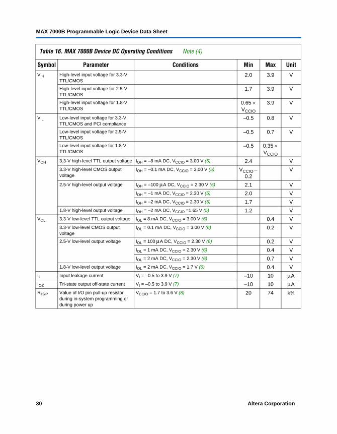
Table 15. MAX 7000B Device Recommended Operating Conditions
Symbol Parameter Conditions Min Max UnitVCCINT Supply voltage for internal logic and
input buffers(10) 2.375 2.625 V
VCCIO Supply voltage for output drivers, 3.3-V operation
3.0 3.6 V
Supply voltage for output drivers, 2.5-V operation
2.375 2.625 V
Supply voltage for output drivers, 1.8-V operation
1.71 1.89 V
VCCISP Supply voltage during in-system programming
2.375 2.625 V
VI Input voltage (3) –0.5 3.9 V
VO Output voltage 0 VCCIO V
TA Ambient temperature For commercial use 0 70 ° C
For industrial use (11) –40 85 ° C
TJ Junction temperature For commercial use 0 90 ° C
For industrial use (11) –40 105 ° C
tR Input rise time 40 ns
tF Input fall time 40 ns
Altera Corporation 29
MAX 7000B Programmable Logic Device Data Sheet
Table 16. MAX 7000B Device DC Operating Conditions Note (4)
Symbol Parameter Conditions Min Max UnitVIH High-level input voltage for 3.3-V
TTL/CMOS2.0 3.9 V
High-level input voltage for 2.5-V TTL/CMOS
1.7 3.9 V
High-level input voltage for 1.8-V TTL/CMOS
0.65 × VCCIO
3.9 V
VIL Low-level input voltage for 3.3-V TTL/CMOS and PCI compliance
–0.5 0.8 V
Low-level input voltage for 2.5-V TTL/CMOS
–0.5 0.7 V
Low-level input voltage for 1.8-V TTL/CMOS
–0.5 0.35 × VCCIO
VOH 3.3-V high-level TTL output voltage IOH = –8 mA DC, VCCIO = 3.00 V (5) 2.4 V
3.3-V high-level CMOS output voltage
IOH = –0.1 mA DC, VCCIO = 3.00 V (5) VCCIO – 0.2
V
2.5-V high-level output voltage IOH = –100 μA DC, VCCIO = 2.30 V (5) 2.1 V
IOH = –1 mA DC, VCCIO = 2.30 V (5) 2.0 V
IOH = –2 mA DC, VCCIO = 2.30 V (5) 1.7 V
1.8-V high-level output voltage IOH = –2 mA DC, VCCIO =1.65 V (5) 1.2 V
VOL 3.3-V low-level TTL output voltage IOL = 8 mA DC, VCCIO = 3.00 V (6) 0.4 V
3.3-V low-level CMOS output voltage
IOL = 0.1 mA DC, VCCIO = 3.00 V (6) 0.2 V
2.5-V low-level output voltage IOL = 100 μA DC, VCCIO = 2.30 V (6) 0.2 V
IOL = 1 mA DC, VCCIO = 2.30 V (6) 0.4 V
IOL = 2 mA DC, VCCIO = 2.30 V (6) 0.7 V
1.8-V low-level output voltage IOL = 2 mA DC, VCCIO = 1.7 V (6) 0.4 V
II Input leakage current VI = –0.5 to 3.9 V (7) –10 10 μA
IOZ Tri-state output off-state current VI = –0.5 to 3.9 V (7) –10 10 μA
RI S P Value of I/O pin pull-up resistor during in-system programming or during power up
VCCIO = 1.7 to 3.6 V (8) 20 74 k¾
30 Altera Corporation
MAX 7000B Programmable Logic Device Data Sheet
Notes to tables:(1) See the Operating Requirements for Altera Devices Data Sheet. (2) Minimum DC input voltage is –0.5 V. During transitions, the inputs may undershoot to –2.0 V or overshoot to 4.6 V
for input currents less than 100 mA and periods shorter than 20 ns.(3) All pins, including dedicated inputs, I/O pins, and JTAG pins, may be driven before VCCINT and VCCIO are
powered.(4) These values are specified under the Recommended Operating Conditions in Table 15 on page 29.(5) The parameter is measured with 50% of the outputs each sourcing the specified current. The IOH parameter refers
to high-level TTL or CMOS output current.(6) The parameter is measured with 50% of the outputs each sinking the specified current. The IOL parameter refers to
low-level TTL or CMOS output current.(7) This value is specified for normal device operation. During power-up, the maximum leakage current is ±300 μA.(8) This pull-up exists while devices are being programmed in-system and in unprogrammed devices during
power-up. The pull-up resistor is from the pins to VCCIO.(9) Capacitance is measured at 25° C and is sample-tested only. Two of the dedicated input pins (OE1 and GCLRN) have
a maximum capacitance of 15 pF.(10) The POR time for all 7000B devices does not exceed 100 μs. The sufficient VCCINT voltage level for POR is 2.375 V.
The device is fully initialized within the POR time after VCCINT reaches the sufficient POR voltage level.(11) These devices support in-system programming for –40° to 100° C. For in-system programming support between
–40° and 0° C, contact Altera Applications.
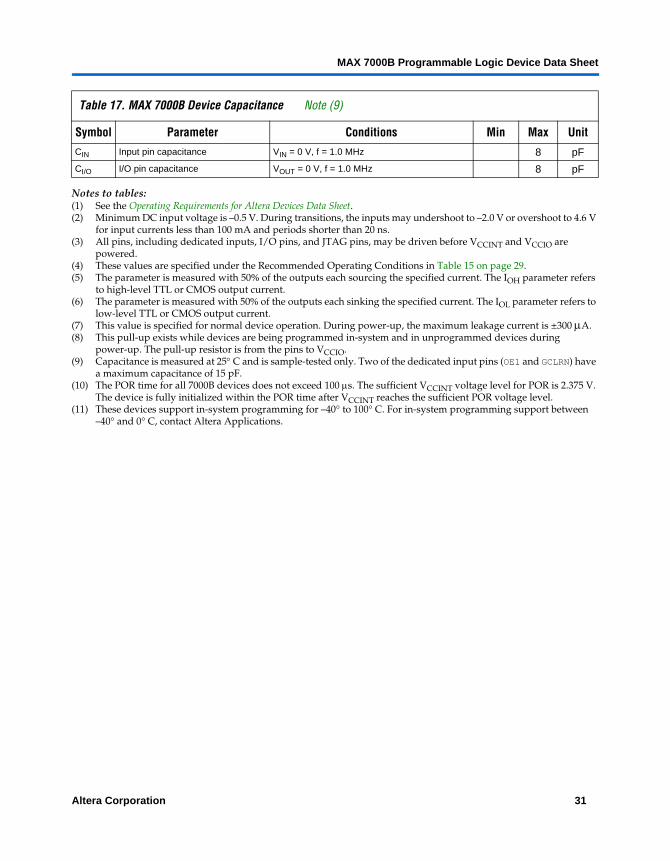
Table 17. MAX 7000B Device Capacitance Note (9)
Symbol Parameter Conditions Min Max UnitCIN Input pin capacitance VIN = 0 V, f = 1.0 MHz 8 pF
CI/O I/O pin capacitance VOUT = 0 V, f = 1.0 MHz 8 pF
Altera Corporation 31
MAX 7000B Programmable Logic Device Data Sheet
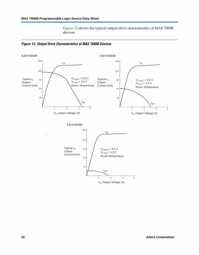
Figure 12 shows the typical output drive characteristics of MAX 7000B devices.
Figure 12. Output Drive Characteristics of MAX 7000B Devices
VO Output Voltage (V)
1 2 3 4
30
60
90
IOL
IOH
VCCINT = 2.5 VVCCIO = 3.0 VRoom Temperature
120
150
Typical I OutputCurrent (mA)
O
VO Output Voltage (V)
1 2 3 4
VCCINT = 2.5 VVCCIO = 2.5 V
IOL
IOH
Room Temperature
2.5-V VCCIO3.3-V VCCIO
Typical I OutputCurrent (mA)
O
30
60
90
120
150
VO Output Voltage (V)
1 2 3
VCCINT = 2.5 VVCCIO = 1.8 V
IOL
IOH
Room Temperature
1.8-V VCCIO
Typical I OutputCurrent (mA)
O
30
60
90
120
150
4
32 Altera Corporation
MAX 7000B Programmable Logic Device Data Sheet
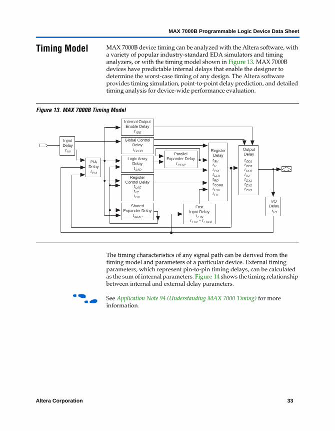
Timing Model MAX 7000B device timing can be analyzed with the Altera software, with a variety of popular industry-standard EDA simulators and timing analyzers, or with the timing model shown in Figure 13. MAX 7000B devices have predictable internal delays that enable the designer to determine the worst-case timing of any design. The Altera software provides timing simulation, point-to-point delay prediction, and detailed timing analysis for device-wide performance evaluation.
Figure 13. MAX 7000B Timing Model
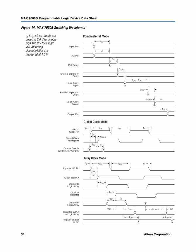
The timing characteristics of any signal path can be derived from the timing model and parameters of a particular device. External timing parameters, which represent pin-to-pin timing delays, can be calculated as the sum of internal parameters. Figure 14 shows the timing relationship between internal and external delay parameters.
f See Application Note 94 (Understanding MAX 7000 Timing) for more information.
Logic ArrayDelayt LAD
OutputDelay
tOD3
tOD2
tOD1
tXZ
Zt X1tZX2tZX3
InputDelay
t I N RegisterDelaytSUtHtPREtCLRtRDtCOMBtFSUtFH
PIADelaytPIA
SharedExpander Delay
tSEXP
RegisterControl Delay
t LACt ICtEN
I/ODelay
t IO
Global ControlDelaytGLOB
Internal OutputEnable Delay
t IOE
ParallelExpander Delay
tPEXP
FastInput Delay
tF INtF IN tF IND+
Altera Corporation 33
MAX 7000B Programmable Logic Device Data Sheet
Figure 14. MAX 7000B Switching Waveforms
Combinatorial Mode
Input Pin
I/O Pin
PIA Delay
Shared ExpanderDelay
Logic ArrayInput
Parallel ExpanderDelay
Logic ArrayOutput
Output Pin
tIN
tLAC , tLAD
tPIA
tOD
tPEXP
tIO
tSEXP
tCOMB
Global Clock Mode
GlobalClock Pin
Global Clockat Register
Data or Enable(Logic Array Output)
tFtCH tCLtR
tINtGLOB
tSU tH
Array Clock Mode
Input or I/O Pin
Clock into PIA
Clock intoLogic Array
Clock atRegister
Data fromLogic Array
Register to PIA to Logic Array
Register Outputto Pin
tFtR tACH tACL
tSU
tINtIO
tRD tPIAtCLR , tPRE
tH
tPIA
tIC
tPIA
tOD tOD
tR & tF < 2 ns. Inputs are driven at 3.0 V for a logic high and 0 V for a logic low. All timing characteristics aremeasured at 1.5 V.
34 Altera Corporation
MAX 7000B Programmable Logic Device Data Sheet
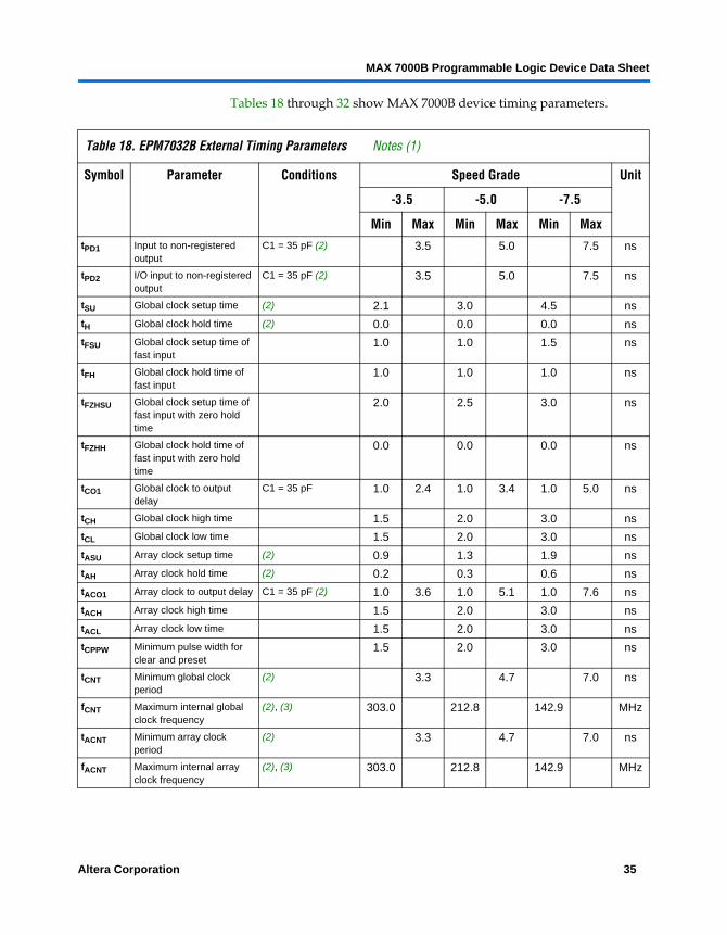
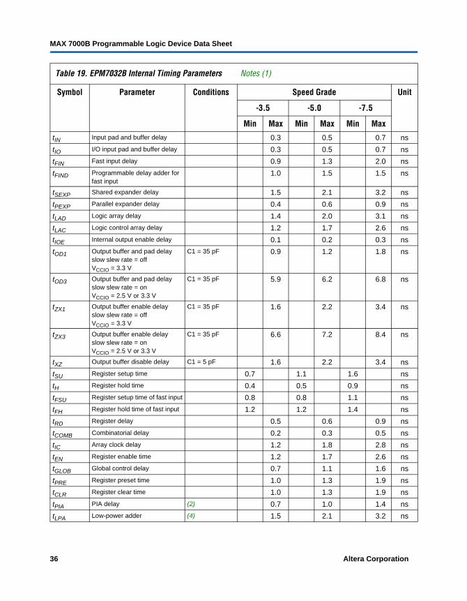
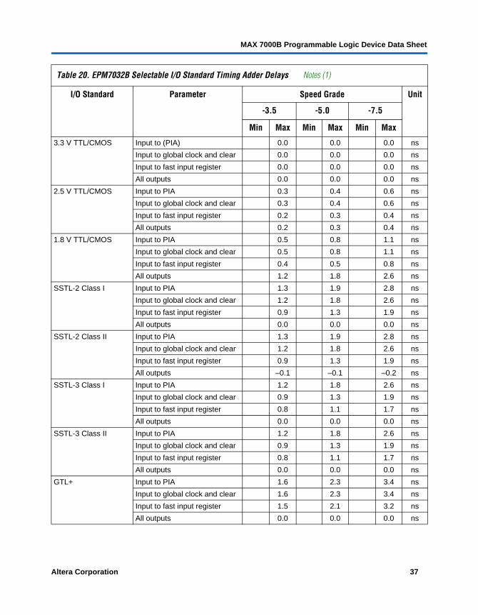
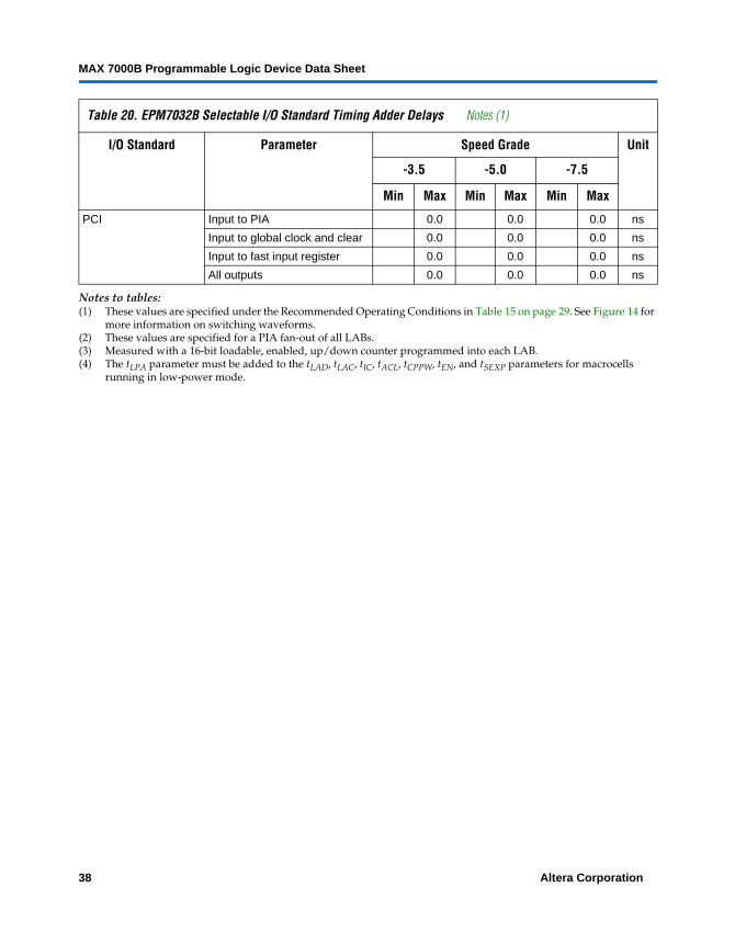
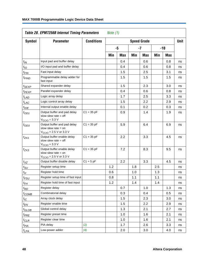
Tables 18 through 32 show MAX 7000B device timing parameters.
Table 18. EPM7032B External Timing Parameters Notes (1)
Symbol Parameter Conditions Speed Grade Unit
-3.5 -5.0 -7.5
Min Max Min Max Min MaxtPD1 Input to non-registered
outputC1 = 35 pF (2) 3.5 5.0 7.5 ns
tPD2 I/O input to non-registered output
C1 = 35 pF (2) 3.5 5.0 7.5 ns
tSU Global clock setup time (2) 2.1 3.0 4.5 ns
tH Global clock hold time (2) 0.0 0.0 0.0 ns
tFSU Global clock setup time of fast input
1.0 1.0 1.5 ns
tFH Global clock hold time of fast input
1.0 1.0 1.0 ns
tFZHSU Global clock setup time of fast input with zero hold time
2.0 2.5 3.0 ns
tFZHH Global clock hold time of fast input with zero hold time
0.0 0.0 0.0 ns
tCO1 Global clock to output delay
C1 = 35 pF 1.0 2.4 1.0 3.4 1.0 5.0 ns
tCH Global clock high time 1.5 2.0 3.0 ns
tCL Global clock low time 1.5 2.0 3.0 ns
tASU Array clock setup time (2) 0.9 1.3 1.9 ns
tAH Array clock hold time (2) 0.2 0.3 0.6 ns
tACO1 Array clock to output delay C1 = 35 pF (2) 1.0 3.6 1.0 5.1 1.0 7.6 ns
tACH Array clock high time 1.5 2.0 3.0 ns
tACL Array clock low time 1.5 2.0 3.0 ns
tCPPW Minimum pulse width for clear and preset
1.5 2.0 3.0 ns
tCNT Minimum global clock period
(2) 3.3 4.7 7.0 ns
fCNT Maximum internal global clock frequency
(2), (3) 303.0 212.8 142.9 MHz
tACNT Minimum array clock period
(2) 3.3 4.7 7.0 ns
fACNT Maximum internal array clock frequency
(2), (3) 303.0 212.8 142.9 MHz
Altera Corporation 35
MAX 7000B Programmable Logic Device Data Sheet
Table 19. EPM7032B Internal Timing Parameters Notes (1)
Symbol Parameter Conditions Speed Grade Unit
-3.5 -5.0 -7.5
Min Max Min Max Min Max
tIN Input pad and buffer delay 0.3 0.5 0.7 ns
tIO I/O input pad and buffer delay 0.3 0.5 0.7 ns
tFIN Fast input delay 0.9 1.3 2.0 ns
tFIND Programmable delay adder for fast input
1.0 1.5 1.5 ns
tSEXP Shared expander delay 1.5 2.1 3.2 ns
tPEXP Parallel expander delay 0.4 0.6 0.9 ns
tLAD Logic array delay 1.4 2.0 3.1 ns
tLAC Logic control array delay 1.2 1.7 2.6 ns
tIOE Internal output enable delay 0.1 0.2 0.3 ns
tOD1 Output buffer and pad delayslow slew rate = off VCCIO = 3.3 V
C1 = 35 pF 0.9 1.2 1.8 ns
tOD3 Output buffer and pad delay slow slew rate = on VCCIO = 2.5 V or 3.3 V
C1 = 35 pF 5.9 6.2 6.8 ns
tZX1 Output buffer enable delayslow slew rate = off VCCIO = 3.3 V
C1 = 35 pF 1.6 2.2 3.4 ns
tZX3 Output buffer enable delayslow slew rate = onVCCIO = 2.5 V or 3.3 V
C1 = 35 pF 6.6 7.2 8.4 ns
tXZ Output buffer disable delay C1 = 5 pF 1.6 2.2 3.4 ns
tSU Register setup time 0.7 1.1 1.6 ns
tH Register hold time 0.4 0.5 0.9 ns
tFSU Register setup time of fast input 0.8 0.8 1.1 ns
tFH Register hold time of fast input 1.2 1.2 1.4 ns
tRD Register delay 0.5 0.6 0.9 ns
tCOMB Combinatorial delay 0.2 0.3 0.5 ns
tIC Array clock delay 1.2 1.8 2.8 ns
tEN Register enable time 1.2 1.7 2.6 ns
tGLOB Global control delay 0.7 1.1 1.6 ns
tPRE Register preset time 1.0 1.3 1.9 ns
tCLR Register clear time 1.0 1.3 1.9 ns
tPIA PIA delay (2) 0.7 1.0 1.4 ns
tLPA Low-power adder (4) 1.5 2.1 3.2 ns
36 Altera Corporation
MAX 7000B Programmable Logic Device Data Sheet
Table 20. EPM7032B Selectable I/O Standard Timing Adder Delays Notes (1)
I/O Standard Parameter Speed Grade Unit
-3.5 -5.0 -7.5
Min Max Min Max Min Max
3.3 V TTL/CMOS Input to (PIA) 0.0 0.0 0.0 ns
Input to global clock and clear 0.0 0.0 0.0 ns
Input to fast input register 0.0 0.0 0.0 ns
All outputs 0.0 0.0 0.0 ns
2.5 V TTL/CMOS Input to PIA 0.3 0.4 0.6 ns
Input to global clock and clear 0.3 0.4 0.6 ns
Input to fast input register 0.2 0.3 0.4 ns
All outputs 0.2 0.3 0.4 ns
1.8 V TTL/CMOS Input to PIA 0.5 0.8 1.1 ns
Input to global clock and clear 0.5 0.8 1.1 ns
Input to fast input register 0.4 0.5 0.8 ns
All outputs 1.2 1.8 2.6 ns
SSTL-2 Class I Input to PIA 1.3 1.9 2.8 ns
Input to global clock and clear 1.2 1.8 2.6 ns
Input to fast input register 0.9 1.3 1.9 ns
All outputs 0.0 0.0 0.0 ns
SSTL-2 Class II Input to PIA 1.3 1.9 2.8 ns
Input to global clock and clear 1.2 1.8 2.6 ns
Input to fast input register 0.9 1.3 1.9 ns
All outputs –0.1 –0.1 –0.2 ns
SSTL-3 Class I Input to PIA 1.2 1.8 2.6 ns
Input to global clock and clear 0.9 1.3 1.9 ns
Input to fast input register 0.8 1.1 1.7 ns
All outputs 0.0 0.0 0.0 ns
SSTL-3 Class II Input to PIA 1.2 1.8 2.6 ns
Input to global clock and clear 0.9 1.3 1.9 ns
Input to fast input register 0.8 1.1 1.7 ns
All outputs 0.0 0.0 0.0 ns
GTL+ Input to PIA 1.6 2.3 3.4 ns
Input to global clock and clear 1.6 2.3 3.4 ns
Input to fast input register 1.5 2.1 3.2 ns
All outputs 0.0 0.0 0.0 ns
Altera Corporation 37
MAX 7000B Programmable Logic Device Data Sheet
Notes to tables:(1) These values are specified under the Recommended Operating Conditions in Table 15 on page 29. See Figure 14 for
more information on switching waveforms.(2) These values are specified for a PIA fan-out of all LABs.(3) Measured with a 16-bit loadable, enabled, up/down counter programmed into each LAB. (4) The tLPA parameter must be added to the tLAD, tLAC, tIC, tACL, tCPPW, tEN, and tSEXP parameters for macrocells
running in low-power mode.
PCI Input to PIA 0.0 0.0 0.0 ns
Input to global clock and clear 0.0 0.0 0.0 ns
Input to fast input register 0.0 0.0 0.0 ns
All outputs 0.0 0.0 0.0 ns
Table 20. EPM7032B Selectable I/O Standard Timing Adder Delays Notes (1)
I/O Standard Parameter Speed Grade Unit
-3.5 -5.0 -7.5
Min Max Min Max Min Max
38 Altera Corporation
MAX 7000B Programmable Logic Device Data Sheet
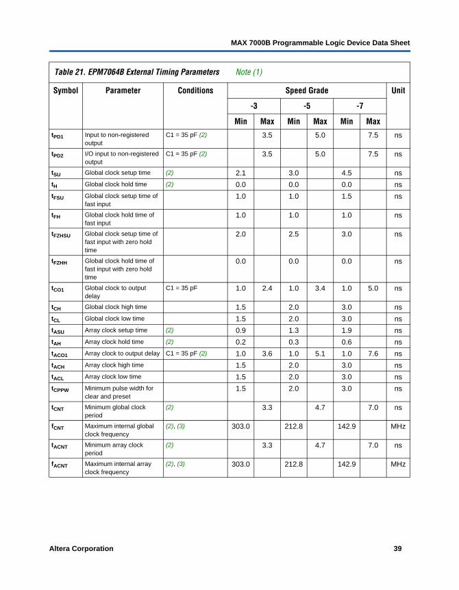
Table 21. EPM7064B External Timing Parameters Note (1)
Symbol Parameter Conditions Speed Grade Unit
-3 -5 -7
Min Max Min Max Min MaxtPD1 Input to non-registered
outputC1 = 35 pF (2) 3.5 5.0 7.5 ns
tPD2 I/O input to non-registered output
C1 = 35 pF (2) 3.5 5.0 7.5 ns
tSU Global clock setup time (2) 2.1 3.0 4.5 ns
tH Global clock hold time (2) 0.0 0.0 0.0 ns
tFSU Global clock setup time of fast input
1.0 1.0 1.5 ns
tFH Global clock hold time of fast input
1.0 1.0 1.0 ns
tFZHSU Global clock setup time of fast input with zero hold time
2.0 2.5 3.0 ns
tFZHH Global clock hold time of fast input with zero hold time
0.0 0.0 0.0 ns
tCO1 Global clock to output delay
C1 = 35 pF 1.0 2.4 1.0 3.4 1.0 5.0 ns
tCH Global clock high time 1.5 2.0 3.0 ns
tCL Global clock low time 1.5 2.0 3.0 ns
tASU Array clock setup time (2) 0.9 1.3 1.9 ns
tAH Array clock hold time (2) 0.2 0.3 0.6 ns
tACO1 Array clock to output delay C1 = 35 pF (2) 1.0 3.6 1.0 5.1 1.0 7.6 ns
tACH Array clock high time 1.5 2.0 3.0 ns
tACL Array clock low time 1.5 2.0 3.0 ns
tCPPW Minimum pulse width for clear and preset
1.5 2.0 3.0 ns
tCNT Minimum global clock period
(2) 3.3 4.7 7.0 ns
fCNT Maximum internal global clock frequency
(2), (3) 303.0 212.8 142.9 MHz
tACNT Minimum array clock period
(2) 3.3 4.7 7.0 ns
fACNT Maximum internal array clock frequency
(2), (3) 303.0 212.8 142.9 MHz
Altera Corporation 39
MAX 7000B Programmable Logic Device Data Sheet
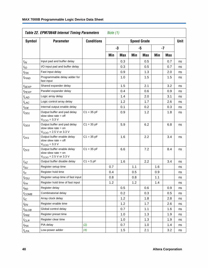
Table 22. EPM7064B Internal Timing Parameters Note (1)
Symbol Parameter Conditions Speed Grade Unit
-3 -5 -7
Min Max Min Max Min Max
tIN Input pad and buffer delay 0.3 0.5 0.7 ns
tIO I/O input pad and buffer delay 0.3 0.5 0.7 ns
tFIN Fast input delay 0.9 1.3 2.0 ns
tFIND Programmable delay adder for fast input
1.0 1.5 1.5 ns
tSEXP Shared expander delay 1.5 2.1 3.2 ns
tPEXP Parallel expander delay 0.4 0.6 0.9 ns
tLAD Logic array delay 1.4 2.0 3.1 ns
tLAC Logic control array delay 1.2 1.7 2.6 ns
tIOE Internal output enable delay 0.1 0.2 0.3 ns
tOD1 Output buffer and pad delayslow slew rate = off VCCIO = 3.3 V
C1 = 35 pF 0.9 1.2 1.8 ns
tOD3 Output buffer and pad delay slow slew rate = on VCCIO = 2.5 V or 3.3 V
C1 = 35 pF 5.9 6.2 6.8 ns
tZX1 Output buffer enable delayslow slew rate = off VCCIO = 3.3 V
C1 = 35 pF 1.6 2.2 3.4 ns
tZX3 Output buffer enable delayslow slew rate = onVCCIO = 2.5 V or 3.3 V
C1 = 35 pF 6.6 7.2 8.4 ns
tXZ Output buffer disable delay C1 = 5 pF 1.6 2.2 3.4 ns
tSU Register setup time 0.7 1.1 1.6 ns
tH Register hold time 0.4 0.5 0.9 ns
tFSU Register setup time of fast input 0.8 0.8 1.1 ns
tFH Register hold time of fast input 1.2 1.2 1.4 ns
tRD Register delay 0.5 0.6 0.9 ns
tCOMB Combinatorial delay 0.2 0.3 0.5 ns
tIC Array clock delay 1.2 1.8 2.8 ns
tEN Register enable time 1.2 1.7 2.6 ns
tGLOB Global control delay 0.7 1.1 1.6 ns
tPRE Register preset time 1.0 1.3 1.9 ns
tCLR Register clear time 1.0 1.3 1.9 ns
tPIA PIA delay (2) 0.7 1.0 1.4 ns
tLPA Low-power adder (4) 1.5 2.1 3.2 ns
40 Altera Corporation
MAX 7000B Programmable Logic Device Data Sheet
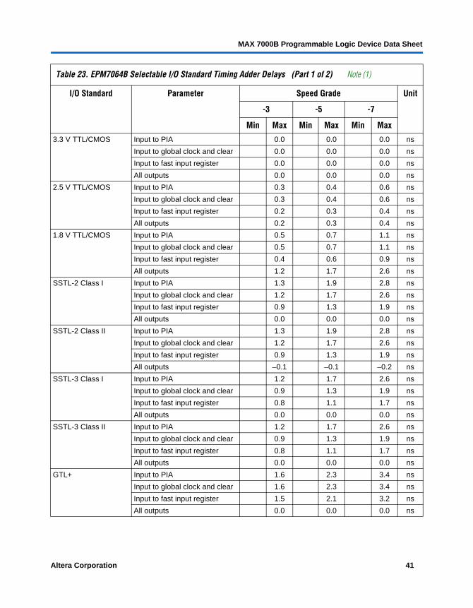
Table 23. EPM7064B Selectable I/O Standard Timing Adder Delays (Part 1 of 2) Note (1)
I/O Standard Parameter Speed Grade Unit
-3 -5 -7
Min Max Min Max Min Max
3.3 V TTL/CMOS Input to PIA 0.0 0.0 0.0 ns
Input to global clock and clear 0.0 0.0 0.0 ns
Input to fast input register 0.0 0.0 0.0 ns
All outputs 0.0 0.0 0.0 ns
2.5 V TTL/CMOS Input to PIA 0.3 0.4 0.6 ns
Input to global clock and clear 0.3 0.4 0.6 ns
Input to fast input register 0.2 0.3 0.4 ns
All outputs 0.2 0.3 0.4 ns
1.8 V TTL/CMOS Input to PIA 0.5 0.7 1.1 ns
Input to global clock and clear 0.5 0.7 1.1 ns
Input to fast input register 0.4 0.6 0.9 ns
All outputs 1.2 1.7 2.6 ns
SSTL-2 Class I Input to PIA 1.3 1.9 2.8 ns
Input to global clock and clear 1.2 1.7 2.6 ns
Input to fast input register 0.9 1.3 1.9 ns
All outputs 0.0 0.0 0.0 ns
SSTL-2 Class II Input to PIA 1.3 1.9 2.8 ns
Input to global clock and clear 1.2 1.7 2.6 ns
Input to fast input register 0.9 1.3 1.9 ns
All outputs –0.1 –0.1 –0.2 ns
SSTL-3 Class I Input to PIA 1.2 1.7 2.6 ns
Input to global clock and clear 0.9 1.3 1.9 ns
Input to fast input register 0.8 1.1 1.7 ns
All outputs 0.0 0.0 0.0 ns
SSTL-3 Class II Input to PIA 1.2 1.7 2.6 ns
Input to global clock and clear 0.9 1.3 1.9 ns
Input to fast input register 0.8 1.1 1.7 ns
All outputs 0.0 0.0 0.0 ns
GTL+ Input to PIA 1.6 2.3 3.4 ns
Input to global clock and clear 1.6 2.3 3.4 ns
Input to fast input register 1.5 2.1 3.2 ns
All outputs 0.0 0.0 0.0 ns
Altera Corporation 41
MAX 7000B Programmable Logic Device Data Sheet
Notes to tables:(1) These values are specified under the Recommended Operating Conditions in Table 15 on page 29. See Figure 14 for
more information on switching waveforms.(2) These values are specified for a PIA fan-out of all LABs.(3) Measured with a 16-bit loadable, enabled, up/down counter programmed into each LAB. (4) The tLPA parameter must be added to the tLAD, tLAC, tIC, tACL, tCPPW, tEN, and tSEXP parameters for macrocells
running in low-power mode.
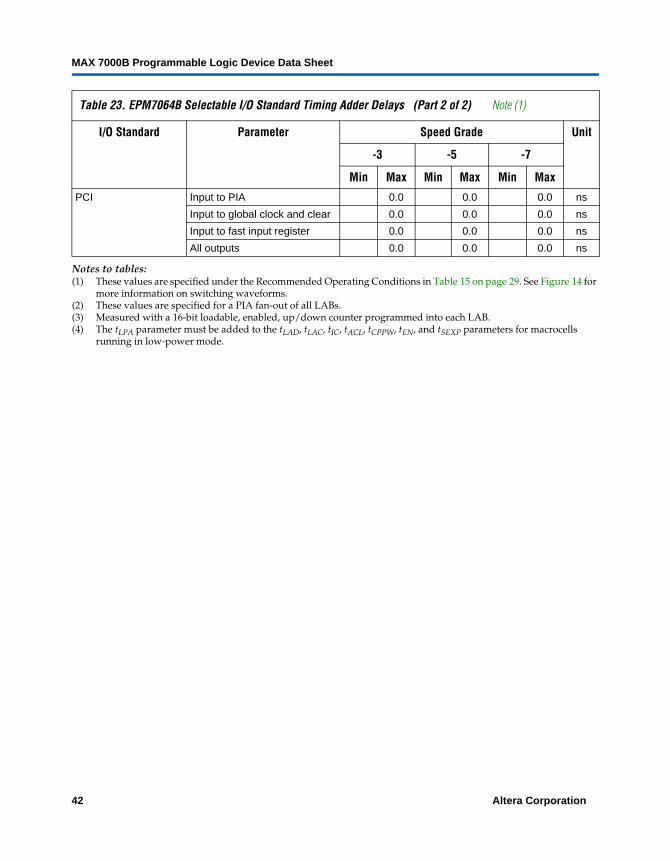
PCI Input to PIA 0.0 0.0 0.0 ns
Input to global clock and clear 0.0 0.0 0.0 ns
Input to fast input register 0.0 0.0 0.0 ns
All outputs 0.0 0.0 0.0 ns
Table 23. EPM7064B Selectable I/O Standard Timing Adder Delays (Part 2 of 2) Note (1)
I/O Standard Parameter Speed Grade Unit
-3 -5 -7
Min Max Min Max Min Max
42 Altera Corporation

MAX 7000B Programmable Logic Device Data Sheet
Table 24. EPM7128B External Timing Parameters Note (1)
Symbol Parameter Conditions Speed Grade Unit
-4 -7 -10
Min Max Min Max Min MaxtPD1 Input to non-registered
outputC1 = 35 pF (2) 4.0 7.5 10.0 ns
tPD2 I/O input to non-registered output
C1 = 35 pF (2) 4.0 7.5 10.0 ns
tSU Global clock setup time (2) 2.5 4.5 6.1 ns
tH Global clock hold time (2) 0.0 0.0 0.0 ns
tFSU Global clock setup time of fast input
1.0 1.5 1.5 ns
tFH Global clock hold time of fast input
1.0 1.0 1.0 ns
tFZHSU Global clock setup time of fast input with zero hold time
2.0 3.0 3.0 ns
tFZHH Global clock hold time of fast input with zero hold time
0.0 0.0 0.0 ns
tCO1 Global clock to output delay
C1 = 35 pF 1.0 2.8 1.0 5.7 1.0 7.5 ns
tCH Global clock high time 1.5 3.0 4.0 ns
tCL Global clock low time 1.5 3.0 4.0 ns
tASU Array clock setup time (2) 1.2 2.0 2.8 ns
tAH Array clock hold time (2) 0.2 0.7 0.9 ns
tACO1 Array clock to output delay C1 = 35 pF (2) 1.0 4.1 1.0 8.2 1.0 10.8 ns
tACH Array clock high time 1.5 3.0 4.0 ns
tACL Array clock low time 1.5 3.0 4.0 ns
tCPPW Minimum pulse width for clear and preset
1.5 3.0 4.0 ns
tCNT Minimum global clock period
(2) 4.1 7.9 10.6 ns
fCNT Maximum internal global clock frequency
(2), (3) 243.9 126.6 94.3 MHz
tACNT Minimum array clock period
(2) 4.1 7.9 10.6 ns
fACNT Maximum internal array clock frequency
(2), (3) 243.9 126.6 94.3 MHz
Altera Corporation 43
MAX 7000B Programmable Logic Device Data Sheet
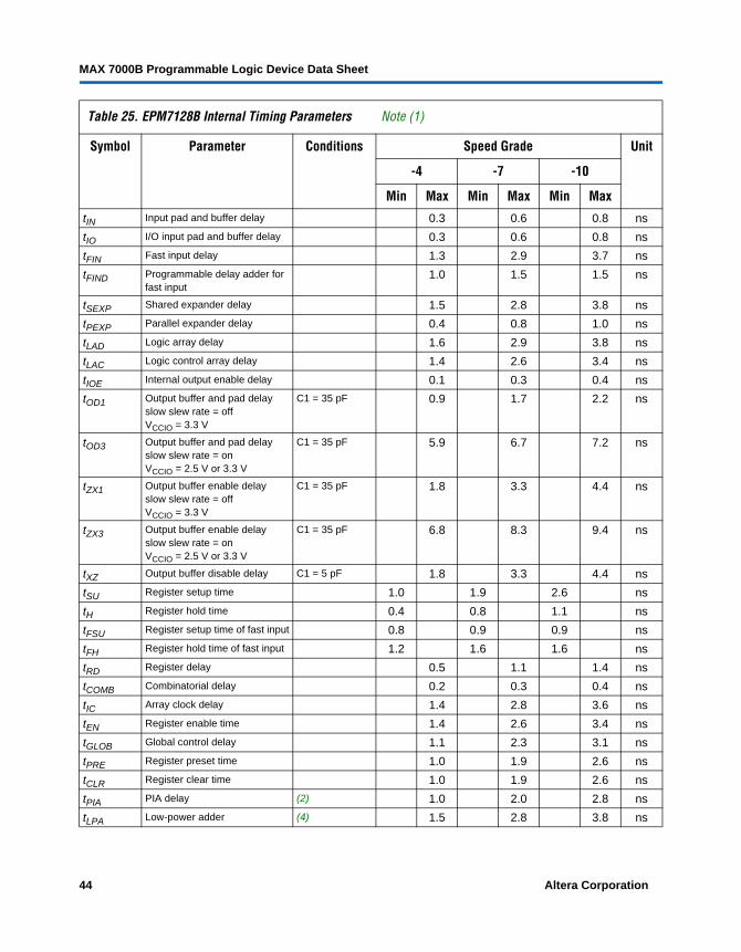
Table 25. EPM7128B Internal Timing Parameters Note (1)
Symbol Parameter Conditions Speed Grade Unit
-4 -7 -10
Min Max Min Max Min Max
tIN Input pad and buffer delay 0.3 0.6 0.8 ns
tIO I/O input pad and buffer delay 0.3 0.6 0.8 ns
tFIN Fast input delay 1.3 2.9 3.7 ns
tFIND Programmable delay adder for fast input
1.0 1.5 1.5 ns
tSEXP Shared expander delay 1.5 2.8 3.8 ns
tPEXP Parallel expander delay 0.4 0.8 1.0 ns
tLAD Logic array delay 1.6 2.9 3.8 ns
tLAC Logic control array delay 1.4 2.6 3.4 ns
tIOE Internal output enable delay 0.1 0.3 0.4 ns
tOD1 Output buffer and pad delayslow slew rate = off VCCIO = 3.3 V
C1 = 35 pF 0.9 1.7 2.2 ns
tOD3 Output buffer and pad delay slow slew rate = on VCCIO = 2.5 V or 3.3 V
C1 = 35 pF 5.9 6.7 7.2 ns
tZX1 Output buffer enable delayslow slew rate = off VCCIO = 3.3 V
C1 = 35 pF 1.8 3.3 4.4 ns
tZX3 Output buffer enable delayslow slew rate = onVCCIO = 2.5 V or 3.3 V
C1 = 35 pF 6.8 8.3 9.4 ns
tXZ Output buffer disable delay C1 = 5 pF 1.8 3.3 4.4 ns
tSU Register setup time 1.0 1.9 2.6 ns
tH Register hold time 0.4 0.8 1.1 ns
tFSU Register setup time of fast input 0.8 0.9 0.9 ns
tFH Register hold time of fast input 1.2 1.6 1.6 ns
tRD Register delay 0.5 1.1 1.4 ns
tCOMB Combinatorial delay 0.2 0.3 0.4 ns
tIC Array clock delay 1.4 2.8 3.6 ns
tEN Register enable time 1.4 2.6 3.4 ns
tGLOB Global control delay 1.1 2.3 3.1 ns
tPRE Register preset time 1.0 1.9 2.6 ns
tCLR Register clear time 1.0 1.9 2.6 ns
tPIA PIA delay (2) 1.0 2.0 2.8 ns
tLPA Low-power adder (4) 1.5 2.8 3.8 ns
44 Altera Corporation
MAX 7000B Programmable Logic Device Data Sheet
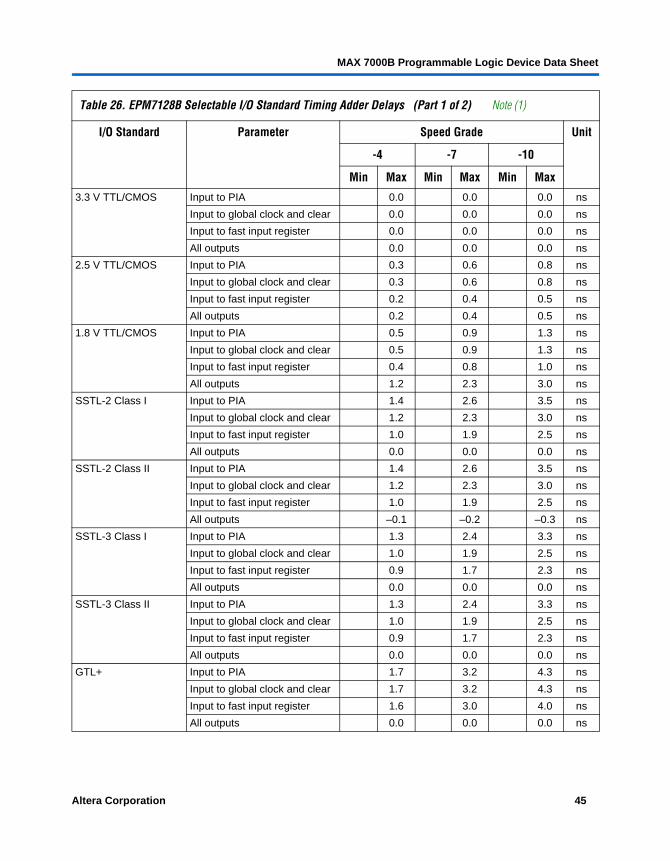
Table 26. EPM7128B Selectable I/O Standard Timing Adder Delays (Part 1 of 2) Note (1)
I/O Standard Parameter Speed Grade Unit
-4 -7 -10
Min Max Min Max Min Max
3.3 V TTL/CMOS Input to PIA 0.0 0.0 0.0 ns
Input to global clock and clear 0.0 0.0 0.0 ns
Input to fast input register 0.0 0.0 0.0 ns
All outputs 0.0 0.0 0.0 ns
2.5 V TTL/CMOS Input to PIA 0.3 0.6 0.8 ns
Input to global clock and clear 0.3 0.6 0.8 ns
Input to fast input register 0.2 0.4 0.5 ns
All outputs 0.2 0.4 0.5 ns
1.8 V TTL/CMOS Input to PIA 0.5 0.9 1.3 ns
Input to global clock and clear 0.5 0.9 1.3 ns
Input to fast input register 0.4 0.8 1.0 ns
All outputs 1.2 2.3 3.0 ns
SSTL-2 Class I Input to PIA 1.4 2.6 3.5 ns
Input to global clock and clear 1.2 2.3 3.0 ns
Input to fast input register 1.0 1.9 2.5 ns
All outputs 0.0 0.0 0.0 ns
SSTL-2 Class II Input to PIA 1.4 2.6 3.5 ns
Input to global clock and clear 1.2 2.3 3.0 ns
Input to fast input register 1.0 1.9 2.5 ns
All outputs –0.1 –0.2 –0.3 ns
SSTL-3 Class I Input to PIA 1.3 2.4 3.3 ns
Input to global clock and clear 1.0 1.9 2.5 ns
Input to fast input register 0.9 1.7 2.3 ns
All outputs 0.0 0.0 0.0 ns
SSTL-3 Class II Input to PIA 1.3 2.4 3.3 ns
Input to global clock and clear 1.0 1.9 2.5 ns
Input to fast input register 0.9 1.7 2.3 ns
All outputs 0.0 0.0 0.0 ns
GTL+ Input to PIA 1.7 3.2 4.3 ns
Input to global clock and clear 1.7 3.2 4.3 ns
Input to fast input register 1.6 3.0 4.0 ns
All outputs 0.0 0.0 0.0 ns
Altera Corporation 45
MAX 7000B Programmable Logic Device Data Sheet
Notes to tables:(1) These values are specified under the Recommended Operating Conditions in Table 15 on page 29. See Figure 14 for
more information on switching waveforms.(2) These values are specified for a PIA fan-out of one LAB (16 macrocells). For each additional LAB fan-out in these
devices, add an additional 0.1 ns to the PIA timing value.(3) Measured with a 16-bit loadable, enabled, up/down counter programmed into each LAB. (4) The tLPA parameter must be added to the tLAD, tLAC, tIC, tACL, tCPPW, tEN, and tSEXP parameters for macrocells
running in low-power mode.
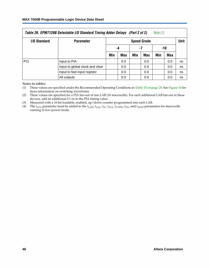
PCI Input to PIA 0.0 0.0 0.0 ns
Input to global clock and clear 0.0 0.0 0.0 ns
Input to fast input register 0.0 0.0 0.0 ns
All outputs 0.0 0.0 0.0 ns
Table 26. EPM7128B Selectable I/O Standard Timing Adder Delays (Part 2 of 2) Note (1)
I/O Standard Parameter Speed Grade Unit
-4 -7 -10
Min Max Min Max Min Max
46 Altera Corporation
MAX 7000B Programmable Logic Device Data Sheet
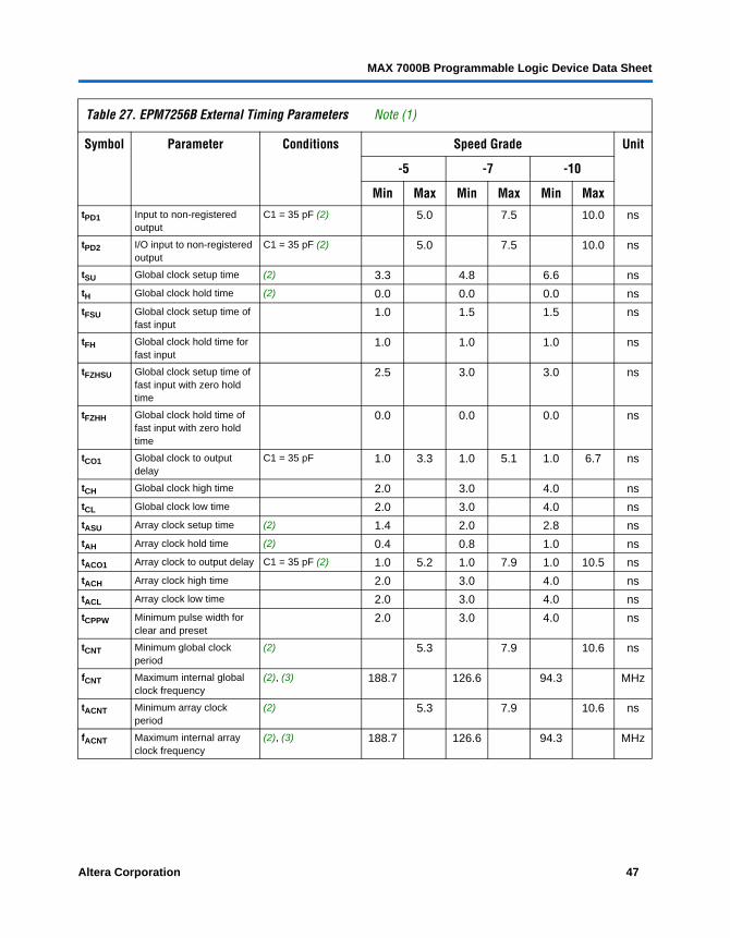
Table 27. EPM7256B External Timing Parameters Note (1)
Symbol Parameter Conditions Speed Grade Unit
-5 -7 -10
Min Max Min Max Min MaxtPD1 Input to non-registered
outputC1 = 35 pF (2) 5.0 7.5 10.0 ns
tPD2 I/O input to non-registered output
C1 = 35 pF (2) 5.0 7.5 10.0 ns
tSU Global clock setup time (2) 3.3 4.8 6.6 ns
tH Global clock hold time (2) 0.0 0.0 0.0 ns
tFSU Global clock setup time of fast input
1.0 1.5 1.5 ns
tFH Global clock hold time for fast input
1.0 1.0 1.0 ns
tFZHSU Global clock setup time of fast input with zero hold time
2.5 3.0 3.0 ns
tFZHH Global clock hold time of fast input with zero hold time
0.0 0.0 0.0 ns
tCO1 Global clock to output delay
C1 = 35 pF 1.0 3.3 1.0 5.1 1.0 6.7 ns
tCH Global clock high time 2.0 3.0 4.0 ns
tCL Global clock low time 2.0 3.0 4.0 ns
tASU Array clock setup time (2) 1.4 2.0 2.8 ns
tAH Array clock hold time (2) 0.4 0.8 1.0 ns
tACO1 Array clock to output delay C1 = 35 pF (2) 1.0 5.2 1.0 7.9 1.0 10.5 ns
tACH Array clock high time 2.0 3.0 4.0 ns
tACL Array clock low time 2.0 3.0 4.0 ns
tCPPW Minimum pulse width for clear and preset
2.0 3.0 4.0 ns
tCNT Minimum global clock period
(2) 5.3 7.9 10.6 ns
fCNT Maximum internal global clock frequency
(2), (3) 188.7 126.6 94.3 MHz
tACNT Minimum array clock period
(2) 5.3 7.9 10.6 ns
fACNT Maximum internal array clock frequency
(2), (3) 188.7 126.6 94.3 MHz
Altera Corporation 47
MAX 7000B Programmable Logic Device Data Sheet
Table 28. EPM7256B Internal Timing Parameters Note (1)
Symbol Parameter Conditions Speed Grade Unit
-5 -7 -10
Min Max Min Max Min Max
tIN Input pad and buffer delay 0.4 0.6 0.8 ns
tIO I/O input pad and buffer delay 0.4 0.6 0.8 ns
tFIN Fast input delay 1.5 2.5 3.1 ns
tFIND Programmable delay adder for fast input
1.5 1.5 1.5 ns
tSEXP Shared expander delay 1.5 2.3 3.0 ns
tPEXP Parallel expander delay 0.4 0.6 0.8 ns
tLAD Logic array delay 1.7 2.5 3.3 ns
tLAC Logic control array delay 1.5 2.2 2.9 ns
tIOE Internal output enable delay 0.1 0.2 0.3 ns
tOD1 Output buffer and pad delayslow slew rate = off VCCIO = 3.3 V
C1 = 35 pF 0.9 1.4 1.9 ns
tOD3 Output buffer and pad delay slow slew rate = on VCCIO = 2.5 V or 3.3 V
C1 = 35 pF 5.9 6.4 6.9 ns
tZX1 Output buffer enable delayslow slew rate = off VCCIO = 3.3 V
C1 = 35 pF 2.2 3.3 4.5 ns
tZX3 Output buffer enable delayslow slew rate = onVCCIO = 2.5 V or 3.3 V
C1 = 35 pF 7.2 8.3 9.5 ns
tXZ Output buffer disable delay C1 = 5 pF 2.2 3.3 4.5 ns
tSU Register setup time 1.2 1.8 2.5 ns
tH Register hold time 0.6 1.0 1.3 ns
tFSU Register setup time of fast input 0.8 1.1 1.1 ns
tFH Register hold time of fast input 1.2 1.4 1.4 ns
tRD Register delay 0.7 1.0 1.3 ns
tCOMB Combinatorial delay 0.3 0.4 0.5 ns
tIC Array clock delay 1.5 2.3 3.0 ns
tEN Register enable time 1.5 2.2 2.9 ns
tGLOB Global control delay 1.3 2.1 2.7 ns
tPRE Register preset time 1.0 1.6 2.1 ns
tCLR Register clear time 1.0 1.6 2.1 ns
tPIA PIA delay (2) 1.7 2.6 3.3 ns
tLPA Low-power adder (4) 2.0 3.0 4.0 ns
48 Altera Corporation

MAX 7000B Programmable Logic Device Data Sheet
Table 29. EPM7256B Selectable I/O Standard Timing Adder Delays (Part 1 of 2) Note (1)
I/O Standard Parameter Speed Grade Unit
-5 -7 -10
Min Max Min Max Min Max
3.3 V TTL/CMOS Input to PIA 0.0 0.0 0.0 ns
Input to global clock and clear 0.0 0.0 0.0 ns
Input to fast input register 0.0 0.0 0.0 ns
All outputs 0.0 0.0 0.0 ns
2.5 V TTL/CMOS Input to PIA 0.4 0.6 0.8 ns
Input to global clock and clear 0.3 0.5 0.6 ns
Input to fast input register 0.2 0.3 0.4 ns
All outputs 0.2 0.3 0.4 ns
1.8 V TTL/CMOS Input to PIA 0.6 0.9 1.2 ns
Input to global clock and clear 0.6 0.9 1.2 ns
Input to fast input register 0.5 0.8 1.0 ns
All outputs 1.3 2.0 2.6 ns
SSTL-2 Class I Input to PIA 1.5 2.3 3.0 ns
Input to global clock and clear 1.3 2.0 2.6 ns
Input to fast input register 1.1 1.7 2.2 ns
All outputs 0.0 0.0 0.0 ns
SSTL-2 Class II Input to PIA 1.5 2.3 3.0 ns
Input to global clock and clear 1.3 2.0 2.6 ns
Input to fast input register 1.1 1.7 2.2 ns
All outputs –0.1 –0.2 –0.2 ns
SSTL-3 Class I Input to PIA 1.4 2.1 2.8 ns
Input to global clock and clear 1.1 1.7 2.2 ns
Input to fast input register 1.0 1.5 2.0 ns
All outputs 0.0 0.0 0.0 ns
SSTL-3 Class II Input to PIA 1.4 2.1 2.8 ns
Input to global clock and clear 1.1 1.7 2.2 ns
Input to fast input register 1.0 1.5 2.0 ns
All outputs 0.0 0.0 0.0 ns
GTL+ Input to PIA 1.8 2.7 3.6 ns
Input to global clock and clear 1.8 2.7 3.6 ns
Input to fast input register 1.7 2.6 3.4 ns
All outputs 0.0 0.0 0.0 ns
Altera Corporation 49
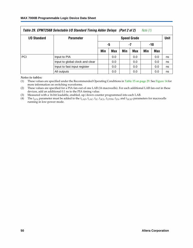
MAX 7000B Programmable Logic Device Data Sheet
Notes to tables:(1) These values are specified under the Recommended Operating Conditions in Table 15 on page 29. See Figure 14 for
more information on switching waveforms.(2) These values are specified for a PIA fan-out of one LAB (16 macrocells). For each additional LAB fan-out in these
devices, add an additional 0.1 ns to the PIA timing value.(3) Measured with a 16-bit loadable, enabled, up/down counter programmed into each LAB. (4) The tLPA parameter must be added to the tLAD, tLAC, tIC, tACL, tCPPW, tEN, and tSEXP parameters for macrocells
running in low-power mode.
PCI Input to PIA 0.0 0.0 0.0 ns
Input to global clock and clear 0.0 0.0 0.0 ns
Input to fast input register 0.0 0.0 0.0 ns
All outputs 0.0 0.0 0.0 ns
Table 29. EPM7256B Selectable I/O Standard Timing Adder Delays (Part 2 of 2) Note (1)
I/O Standard Parameter Speed Grade Unit
-5 -7 -10
Min Max Min Max Min Max
50 Altera Corporation
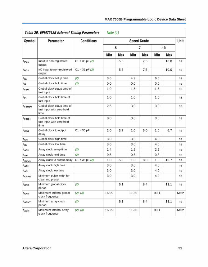
MAX 7000B Programmable Logic Device Data Sheet
Table 30. EPM7512B External Timing Parameters Note (1)
Symbol Parameter Conditions Speed Grade Unit
-5 -7 -10
Min Max Min Max Min MaxtPD1 Input to non-registered
outputC1 = 35 pF (2) 5.5 7.5 10.0 ns
tPD2 I/O input to non-registered output
C1 = 35 pF (2) 5.5 7.5 10.0 ns
tSU Global clock setup time (2) 3.6 4.9 6.5 ns
tH Global clock hold time (2) 0.0 0.0 0.0 ns
tFSU Global clock setup time of fast input
1.0 1.5 1.5 ns
tFH Global clock hold time of fast input
1.0 1.0 1.0 ns
tFZHSU Global clock setup time of fast input with zero hold time
2.5 3.0 3.0 ns
tFZHH Global clock hold time of fast input with zero hold time
0.0 0.0 0.0 ns
tCO1 Global clock to output delay
C1 = 35 pF 1.0 3.7 1.0 5.0 1.0 6.7 ns
tCH Global clock high time 3.0 3.0 4.0 ns
tCL Global clock low time 3.0 3.0 4.0 ns
tASU Array clock setup time (2) 1.4 1.9 2.5 ns
tAH Array clock hold time (2) 0.5 0.6 0.8 ns
tACO1 Array clock to output delay C1 = 35 pF (2) 1.0 5.9 1.0 8.0 1.0 10.7 ns
tACH Array clock high time 3.0 3.0 4.0 ns
tACL Array clock low time 3.0 3.0 4.0 ns
tCPPW Minimum pulse width for clear and preset
3.0 3.0 4.0 ns
tCNT Minimum global clock period
(2) 6.1 8.4 11.1 ns
fCNT Maximum internal global clock frequency
(2), (3) 163.9 119.0 90.1 MHz
tACNT Minimum array clock period
(2) 6.1 8.4 11.1 ns
fACNT Maximum internal array clock frequency
(2), (3) 163.9 119.0 90.1 MHz
Altera Corporation 51

MAX 7000B Programmable Logic Device Data Sheet
Table 31. EPM7512B Internal Timing Parameters Note (1)
Symbol Parameter Conditions Speed Grade Unit
-5 -7 -10
Min Max Min Max Min Max
tIN Input pad and buffer delay 0.3 0.3 0.5 ns
tIO I/O input pad and buffer delay 0.3 0.3 0.5 ns
tFIN Fast input delay 2.2 3.2 4.0 ns
tFIND Programmable delay adder for fast input
1.5 1.5 1.5 ns
tSEXP Shared expander delay 1.5 2.1 2.7 ns
tPEXP Parallel expander delay 0.4 0.5 0.7 ns
tLAD Logic array delay 1.7 2.3 3.0 ns
tLAC Logic control array delay 1.5 2.0 2.6 ns
tIOE Internal output enable delay 0.1 0.2 0.2 ns
tOD1 Output buffer and pad delayslow slew rate = off VCCIO = 3.3 V
C1 = 35 pF 0.9 1.2 1.6 ns
tOD3 Output buffer and pad delay slow slew rate = on VCCIO = 2.5 V or 3.3 V
C1 = 35 pF 5.9 6.2 6.6 ns
tZX1 Output buffer enable delayslow slew rate = off VCCIO = 3.3 V
C1 = 35 pF 2.8 3.8 5.0 ns
tZX3 Output buffer enable delayslow slew rate = onVCCIO = 2.5 V or 3.3 V
C1 = 35 pF 7.8 8.8 10.0 ns
tXZ Output buffer disable delay C1 = 5 pF 2.8 3.8 5.0 ns
tSU Register setup time 1.5 2.0 2.6 ns
tH Register hold time 0.4 0.5 0.7 ns
tFSU Register setup time of fast input 0.8 1.1 1.1 ns
tFH Register hold time of fast input 1.2 1.4 1.4 ns
tRD Register delay 0.5 0.7 1.0 ns
tCOMB Combinatorial delay 0.2 0.3 0.4 ns
tIC Array clock delay 1.8 2.4 3.1 ns
tEN Register enable time 1.5 2.0 2.6 ns
tGLOB Global control delay 2.0 2.8 3.6 ns
tPRE Register preset time 1.0 1.4 1.9 ns
tCLR Register clear time 1.0 1.4 1.9 ns
tPIA PIA delay (2) 2.4 3.4 4.5 ns
tLPA Low-power adder (4) 2.0 2.7 3.6 ns
52 Altera Corporation

MAX 7000B Programmable Logic Device Data Sheet
Table 32. EPM7512B Selectable I/O Standard Timing Adder Delays (Part 1 of 2) Note (1)
I/O Standard Parameter Speed Grade Unit
-5 -7 -10
Min Max Min Max Min Max
3.3 V TTL/CMOS Input to PIA 0.0 0.0 0.0 ns
Input to global clock and clear 0.0 0.0 0.0 ns
Input to fast input register 0.0 0.0 0.0 ns
All outputs 0.0 0.0 0.0 ns
2.5 V TTL/CMOS Input to PIA 0.4 0.5 0.7 ns
Input to global clock and clear 0.3 0.4 0.5 ns
Input to fast input register 0.2 0.3 0.3 ns
All outputs 0.2 0.3 0.3 ns
1.8 V TTL/CMOS Input to PIA 0.7 1.0 1.3 ns
Input to global clock and clear 0.6 0.8 1.0 ns
Input to fast input register 0.5 0.6 0.8 ns
All outputs 1.3 1.8 2.3 ns
SSTL-2 Class I Input to PIA 1.5 2.0 2.7 ns
Input to global clock and clear 1.4 1.9 2.5 ns
Input to fast input register 1.1 1.5 2.0 ns
All outputs 0.0 0.0 0.0 ns
SSTL-2 Class II Input to PIA 1.5 2.0 2.7 ns
Input to global clock and clear 1.4 1.9 2.5 ns
Input to fast input register 1.1 1.5 2.0 ns
All outputs –0.1 –0.1 –0.2 ns
SSTL-3 Class I Input to PIA 1.4 1.9 2.5 ns
Input to global clock and clear 1.2 1.6 2.2 ns
Input to fast input register 1.0 1.4 1.8 ns
All outputs 0.0 0.0 0.0 ns
SSTL-3 Class II Input to PIA 1.4 1.9 2.5 ns
Input to global clock and clear 1.2 1.6 2.2 ns
Input to fast input register 1.0 1.4 1.8 ns
All outputs 0.0 0.0 0.0 ns
GTL+ Input to PIA 1.8 2.5 3.3 ns
Input to global clock and clear 1.9 2.6 3.5 ns
Input to fast input register 1.8 2.5 3.3 ns
All outputs 0.0 0.0 0.0 ns
Altera Corporation 53
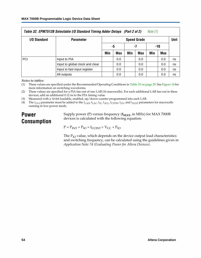
MAX 7000B Programmable Logic Device Data Sheet
Notes to tables:(1) These values are specified under the Recommended Operating Conditions in Table 15 on page 29. See Figure 14 for
more information on switching waveforms.(2) These values are specified for a PIA fan-out of one LAB (16 macrocells). For each additional LAB fan-out in these
devices, add an additional 0.12 ns to the PIA timing value.(3) Measured with a 16-bit loadable, enabled, up/down counter programmed into each LAB. (4) The tLPA parameter must be added to the tLAD, tLAC, tIC, tACL, tCPPW, tEN, and tSEXP parameters for macrocells
running in low-power mode.
Power Consumption
Supply power (P) versus frequency (fMAX, in MHz) for MAX 7000B devices is calculated with the following equation:
P = PINT + PIO = ICCINT × VCC + PIO
The PIO value, which depends on the device output load characteristics and switching frequency, can be calculated using the guidelines given in Application Note 74 (Evaluating Power for Altera Devices).
PCI Input to PIA 0.0 0.0 0.0 ns
Input to global clock and clear 0.0 0.0 0.0 ns
Input to fast input register 0.0 0.0 0.0 ns
All outputs 0.0 0.0 0.0 ns
Table 32. EPM7512B Selectable I/O Standard Timing Adder Delays (Part 2 of 2) Note (1)
I/O Standard Parameter Speed Grade Unit
-5 -7 -10
Min Max Min Max Min Max
54 Altera Corporation
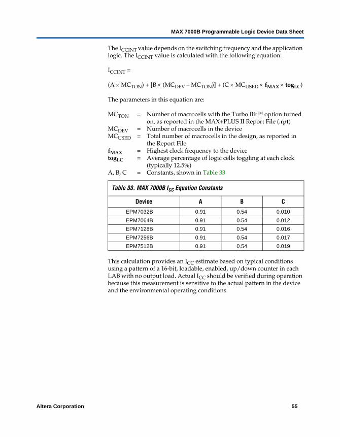
MAX 7000B Programmable Logic Device Data Sheet
The ICCINT value depends on the switching frequency and the application logic. The ICCINT value is calculated with the following equation:
ICCINT =
(A × MCTON) + [B × (MCDEV – MCTON)] + (C × MCUSED × fMAX × togLC)
The parameters in this equation are:
MCTON = Number of macrocells with the Turbo BitTM option turned on, as reported in the MAX+PLUS II Report File (.rpt)
MCDEV = Number of macrocells in the deviceMCUSED = Total number of macrocells in the design, as reported in
the Report FilefMAX = Highest clock frequency to the devicetogLC = Average percentage of logic cells toggling at each clock
(typically 12.5%)A, B, C = Constants, shown in Table 33
This calculation provides an ICC estimate based on typical conditions using a pattern of a 16-bit, loadable, enabled, up/down counter in each LAB with no output load. Actual ICC should be verified during operation because this measurement is sensitive to the actual pattern in the device and the environmental operating conditions.
Table 33. MAX 7000B ICC Equation Constants
Device A B C
EPM7032B 0.91 0.54 0.010
EPM7064B 0.91 0.54 0.012
EPM7128B 0.91 0.54 0.016
EPM7256B 0.91 0.54 0.017
EPM7512B 0.91 0.54 0.019
Altera Corporation 55
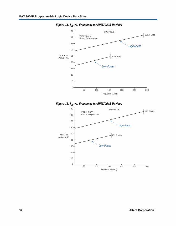
MAX 7000B Programmable Logic Device Data Sheet
Figure 15. ICC vs. Frequency for EPM7032B Devices
Figure 16. ICC vs. Frequency for EPM7064B Devices
100 150 20050
10
5
0
15
20
25
30
35
40
45
250 300
VCC = 2.5 VRoom Temperature
153.8 MHz
285.7 MHz
Frequency (MHz)
Typical ICC
Active (mA)
Low Power
High Speed
EPM7032B
100 150 20050
20
10
0
30
40
50
60
70
80
90
250 300
VCC = 2.5 VRoom Temperature
153.8 MHz
285.7 MHz
Frequency (MHz)
Typical ICC
Active (mA)
Low Power
High Speed
EPM7064B
56 Altera Corporation
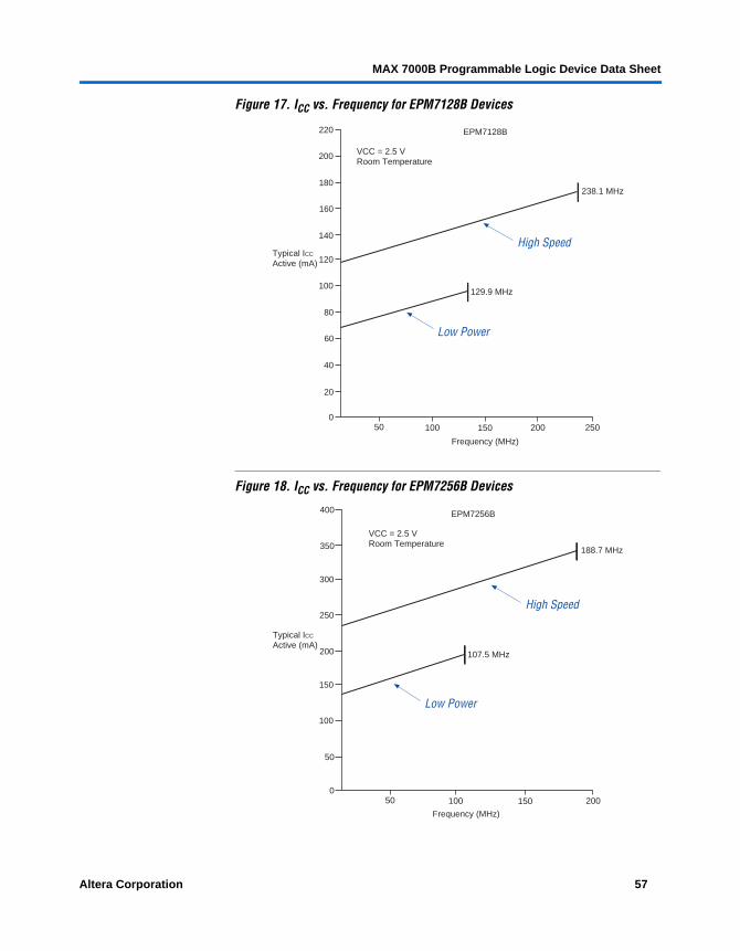
MAX 7000B Programmable Logic Device Data Sheet
Figure 17. ICC vs. Frequency for EPM7128B Devices
Figure 18. ICC vs. Frequency for EPM7256B Devices
100 150 20050
40
20
0
60
80
100
120
140
160
180
200
220
250
VCC = 2.5 VRoom Temperature
129.9 MHz
238.1 MHz
Frequency (MHz)
Typical ICC
Active (mA)
Low Power
High Speed
EPM7128B
100 15050
50
0
100
150
200
250
300
350
400
200
VCC = 2.5 VRoom Temperature
107.5 MHz
188.7 MHz
Frequency (MHz)
Typical ICC
Active (mA)
Low Power
High Speed
EPM7256B
Altera Corporation 57
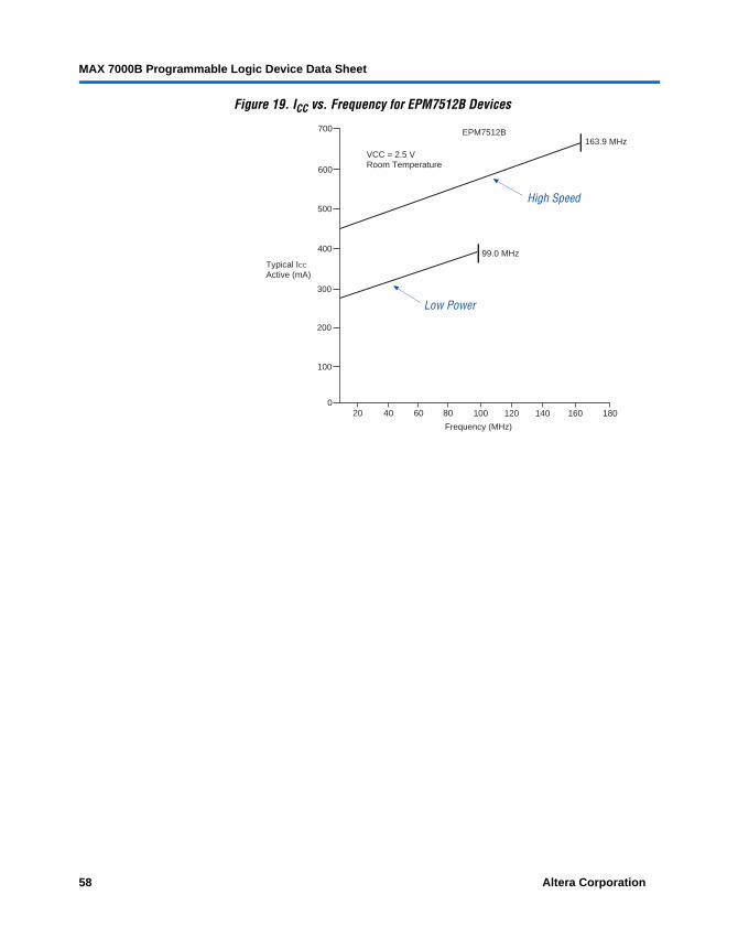
MAX 7000B Programmable Logic Device Data Sheet
Figure 19. ICC vs. Frequency for EPM7512B Devices
80 120400
100
200
300
400
500
600
700
18060 10020 140 160
VCC = 2.5 VRoom Temperature
99.0 MHz
163.9 MHz
Frequency (MHz)
Typical ICC
Active (mA)
Low Power
High Speed
EPM7512B
58 Altera Corporation
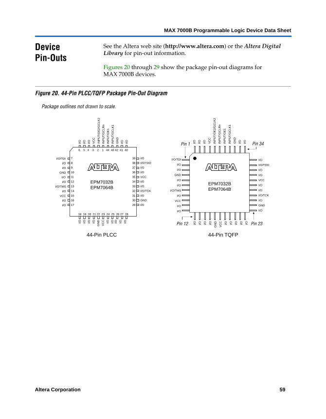
MAX 7000B Programmable Logic Device Data Sheet
Device Pin-Outs
See the Altera web site (http://www.altera.com) or the Altera Digital Library for pin-out information.
Figures 20 through 29 show the package pin-out diagrams for MAX 7000B devices.
Figure 20. 44-Pin PLCC/TQFP Package Pin-Out Diagram
Package outlines not drawn to scale.
44-Pin PLCC
I/O I/O I/O VC
C
INP
UT
/OE
2/G
CLK
2
INP
UT
/GC
LRn
INP
UT
/OE
1
INP
UT
/GC
LK1
GN
D
I/O I/O
I/O
I/O/TDO
I/O
I/O
VCC
I/O
I/O
I/O/TCK
I/O
GND
I/O
I/O I/O I/O I/O
GN
D
VC
C
I/O I/O I/O I/O I/O
6 5 4 3 2 1 44 43 42 41 40
18 19 20 21 22 23 24 25 26 27 28
7
8
9
10
11
12
13
14
15
16
17
39
38
37
36
35
34
33
32
31
30
29
EPM7032BEPM7064B
I/O /TDI
I/O
I/O
GND
I/O
I/O
I/O/TMS
I/O
VCC
I/O
I/O
44-Pin TQFP
Pin 12 Pin 23
Pin 34Pin 1 I/O I/O I/O VC
C
INP
UT
/OE
2/G
CLK
2
INP
UT
/GC
LRn
INP
UT
/OE
1
INP
UT
/GC
LK1
GN
D
I/O I/O
I/O
I/O/TDO
I/O
I/O
VCC
I/O
I/O
I/O/TCK
I/O
GND
I/O
I/O I/O I/O I/O
GN
D
VC
C
I/O I/O I/O I/O I/O
I/O/TDI
I/O
I/O
GND
I/O
I/O
I/O/TMS
I/O
VCC
I/O
I/O
EPM7032BEPM7064B
Altera Corporation 59
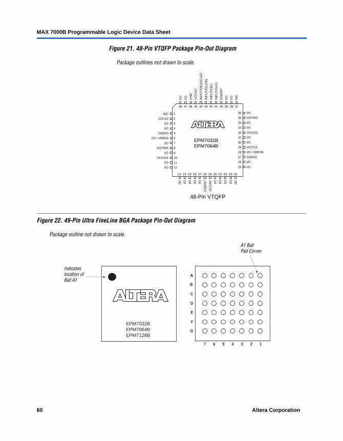
MAX 7000B Programmable Logic Device Data Sheet
Figure 21. 48-Pin VTQFP Package Pin-Out Diagram
Package outlines not drawn to scale.
Figure 22. 49-Pin Ultra FineLine BGA Package Pin-Out Diagram
Package outline not drawn to scale.
I/O
48-Pin VTQFP
I/O I/O GN
D
VC
CIN
T
INP
UT
/OE
2/G
CLK
2
INP
UT
/GC
LRN
INP
UT
/OE
1
INP
UT
/GLK
1
GN
DIN
T
I/O I/O N/C
I/O
I/O/TDO
I/O
I/O
VCCIO2
I/O
I/O
I/O/TCK
I/O / VREFB
GNDIO
I/O
I/O
NC
I/O I/O I/O I/O
GN
DIN
T
VC
CIN
T
I/O I/O I/O I/O NC
48 47 46 45 44 43 42 41 40 39 38 37
13 14 15 16 17 18 19 20 21 22 23 24
1
2
3
4
5
6
7
8
9
10
11
12
36
35
34
33
32
31
30
29
28
27
26
25
EPM7032BEPM7064B
N/C
I/O/TDI
I/O
I/O
GNDIO
I/O / VREFA
I/O
I/O/TMS
I/O
VCCIO1
I/O
Indicateslocation ofBall A1
A1 BallPad Corner
A
B
C
D
E
F
G
7 6 5 4 3 2 1
EPM7032BEPM7064BEPM7128B
60 Altera Corporation
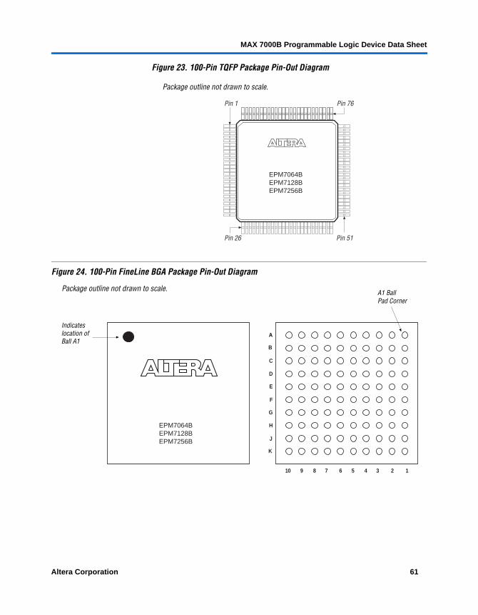
MAX 7000B Programmable Logic Device Data Sheet
Figure 23. 100-Pin TQFP Package Pin-Out Diagram
Package outline not drawn to scale.
Figure 24. 100-Pin FineLine BGA Package Pin-Out Diagram
Pin 1
Pin 26
Pin 76
Pin 51
EPM7064BEPM7128BEPM7256B
Indicateslocation ofBall A1
A1 BallPad Corner
A
B
C
D
E
F
G
H
J
K
10 9 8 7 6 5 4 3 2 1
EPM7064BEPM7128BEPM7256B
Package outline not drawn to scale.
Altera Corporation 61
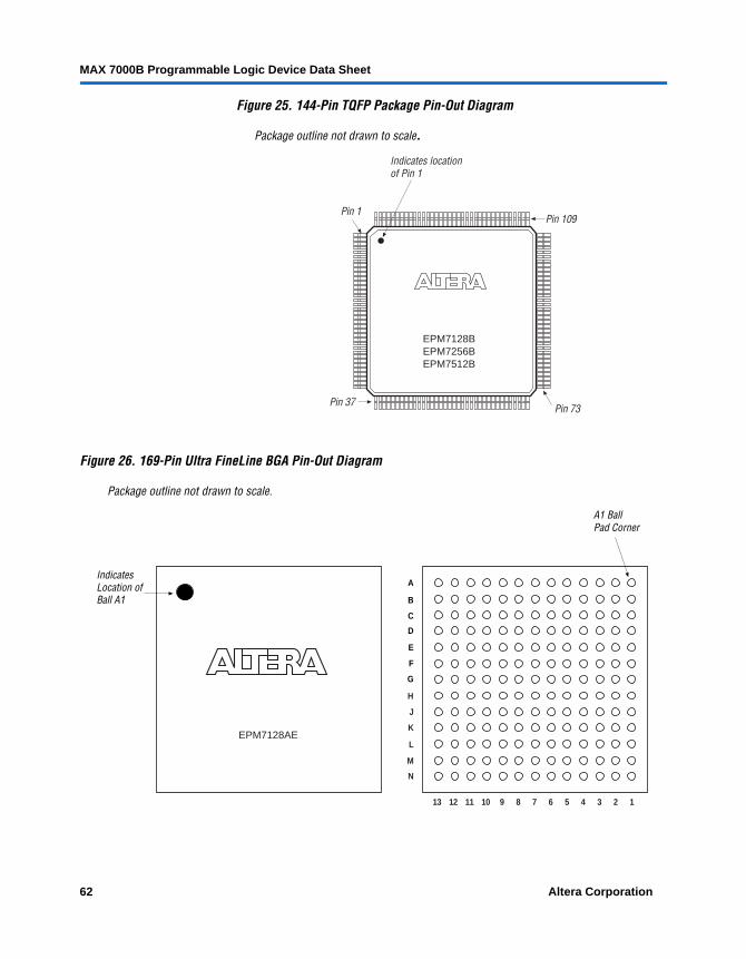
MAX 7000B Programmable Logic Device Data Sheet
Figure 25. 144-Pin TQFP Package Pin-Out Diagram
Package outline not drawn to scale.
Figure 26. 169-Pin Ultra FineLine BGA Pin-Out Diagram
Package outline not drawn to scale.
Indicates locationof Pin 1
Pin 1 Pin 109
Pin 73Pin 37
EPM7128BEPM7256BEPM7512B
IndicatesLocation ofBall A1
A1 BallPad Corner
G
F
E
D
C
B
A
H
J
K
L
M
N
13 12 11 10 9 8 7 6 5 4 3 2 1
EPM7128AE
62 Altera Corporation
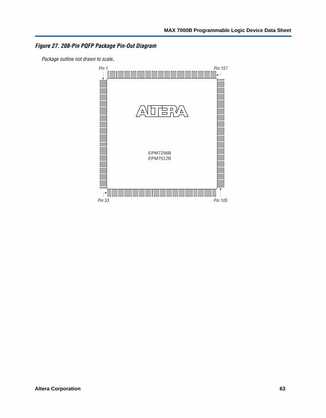
MAX 7000B Programmable Logic Device Data Sheet
Figure 27. 208-Pin PQFP Package Pin-Out Diagram
Package outline not drawn to scale.Pin 1 Pin 157
Pin 105Pin 53
EPM7256BEPM7512B
Altera Corporation 63
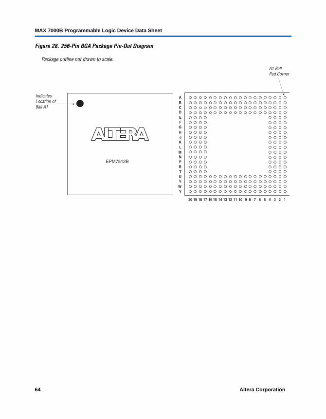
MAX 7000B Programmable Logic Device Data Sheet
Figure 28. 256-Pin BGA Package Pin-Out Diagram
Package outline not drawn to scale.
IndicatesLocation ofBall A1
A1 BallPad Corner
GFEDCBA
HJKLMNPRT
16 15 14 13 12 11 10 9 8 7 6 5 4 3 2 1
EPM7512B
UVWY
17181920
64 Altera Corporation
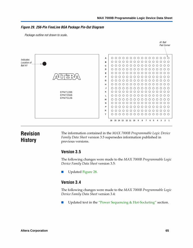
MAX 7000B Programmable Logic Device Data Sheet
Figure 29. 256-Pin FineLine BGA Package Pin-Out Diagram
Package outline not drawn to scale.
Revision History
The information contained in the MAX 7000B Programmable Logic Device Family Data Sheet version 3.5 supersedes information published in previous versions.
Version 3.5
The following changes were made to the MAX 7000B Programmable Logic Device Family Data Sheet version 3.5:
■ Updated Figure 28.
Version 3.4
The following changes were made to the MAX 7000B Programmable Logic Device Family Data Sheet version 3.4:
■ Updated text in the “Power Sequencing & Hot-Socketing” section.
IndicatesLocation ofBall A1
A1 BallPad Corner
G
F
E
D
C
B
A
H
J
K
L
M
N
P
R
T
16 15 14 13 12 11 10 9 8 7 6 5 4 3 2 1
EPM7128BEPM7256BEPM7512B
Altera Corporation 65
MAX 7000B Programmable Logic Device Data Sheet
Copyright © 2003 Altera Corporation. All rights reserved. Altera, The Programmable Solutions Company, thestylized Altera logo, specific device designations, and all other words and logos that are identified astrademarks and/or service marks are, unless noted otherwise, the trademarks and service marks of AlteraCorporation in the U.S. and other countries. All other product or service names are the property of theirrespective holders. Altera products are protected under numerous U.S. and foreign patents and pendingapplications, maskwork rights, and copyrights. Altera warrants performance of its semiconductor products tocurrent specifications in accordance with Altera's standard warranty, but reserves the rightto make changes to any products and services at any time without notice. Altera assumes noresponsibility or liability arising out of the application or use of any information, product, orservice described herein except as expressly agreed to in writing by Altera Corporation.Altera customers are advised to obtain the latest version of device specifications beforerelying on any published information and before placing orders for products or services.
101 Innovation DriveSan Jose, CA 95134(408) 544-7000http://www.altera.comApplications Hotline:(800) 800-EPLDCustomer Marketing:(408) 544-7104Literature Services:[email protected]
Version 3.3
The following changes were made to the MAX 7000B Programmable Logic Device Family Data Sheet version 3.3:
■ Updated Table 3.■ Added Tables 4 through 6.
Version 3.2
The following changes were made to the MAX 7000B Programmable Logic Device Family Data Sheet version 3.2:
■ Updated Note (10) and added ambient temperature (TA) information to Table 15.
Version 3.1
The following changes were made to the MAX 7000B Programmable Logic Device Family Data Sheet version 3.1:
■ Updated VIH and VIL specifications in Table 16.■ Updated leakage current conditions in Table 16.
Version 3.0
The following changes were made to the MAX 7000B Programmable Logic Device Family Data Sheet version 3.0:
■ Updated timing numbers in Table 1.■ Updated Table 16.■ Updated timing in Tables 18, 19, 21, 22, 24, 25, 27, 28, 30, and 31.
66 Altera Corporation
Printed on Recycled Paper.