Embed Size (px)
Citation preview
1
®
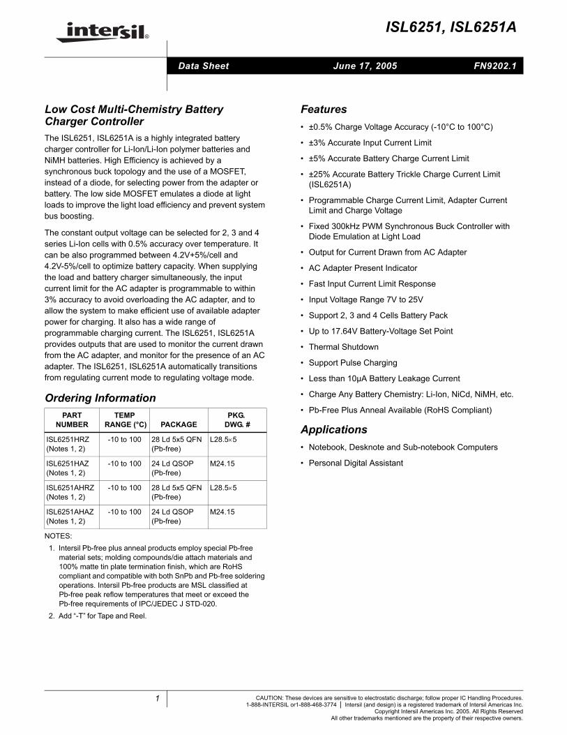
ISL6251, ISL6251AFN9202.1Data Sheet June 17, 2005
Low Cost Multi-Chemistry Battery Charger ControllerThe ISL6251, ISL6251A is a highly integrated battery charger controller for Li-Ion/Li-Ion polymer batteries and NiMH batteries. High Efficiency is achieved by a synchronous buck topology and the use of a MOSFET, instead of a diode, for selecting power from the adapter or battery. The low side MOSFET emulates a diode at light loads to improve the light load efficiency and prevent system bus boosting.
The constant output voltage can be selected for 2, 3 and 4 series Li-Ion cells with 0.5% accuracy over temperature. It can be also programmed between 4.2V+5%/cell and 4.2V-5%/cell to optimize battery capacity. When supplying the load and battery charger simultaneously, the input current limit for the AC adapter is programmable to within 3% accuracy to avoid overloading the AC adapter, and to allow the system to make efficient use of available adapter power for charging. It also has a wide range of programmable charging current. The ISL6251, ISL6251A provides outputs that are used to monitor the current drawn from the AC adapter, and monitor for the presence of an AC adapter. The ISL6251, ISL6251A automatically transitions from regulating current mode to regulating voltage mode.
Features• ±0.5% Charge Voltage Accuracy (-10°C to 100°C)
• ±3% Accurate Input Current Limit
• ±5% Accurate Battery Charge Current Limit
• ±25% Accurate Battery Trickle Charge Current Limit (ISL6251A)
• Programmable Charge Current Limit, Adapter Current Limit and Charge Voltage
• Fixed 300kHz PWM Synchronous Buck Controller with Diode Emulation at Light Load
• Output for Current Drawn from AC Adapter
• AC Adapter Present Indicator
• Fast Input Current Limit Response
• Input Voltage Range 7V to 25V
• Support 2, 3 and 4 Cells Battery Pack
• Up to 17.64V Battery-Voltage Set Point
• Thermal Shutdown
• Support Pulse Charging
• Less than 10µA Battery Leakage Current
• Charge Any Battery Chemistry: Li-Ion, NiCd, NiMH, etc.
• Pb-Free Plus Anneal Available (RoHS Compliant)
Applications• Notebook, Desknote and Sub-notebook Computers
• Personal Digital Assistant
Ordering InformationPART
NUMBERTEMP
RANGE (°C) PACKAGEPKG.
DWG. #
ISL6251HRZ(Notes 1, 2)
-10 to 100 28 Ld 5x5 QFN(Pb-free)
L28.5×5
ISL6251HAZ (Notes 1, 2)
-10 to 100 24 Ld QSOP (Pb-free)
M24.15
ISL6251AHRZ(Notes 1, 2)
-10 to 100 28 Ld 5x5 QFN(Pb-free)
L28.5×5
ISL6251AHAZ (Notes 1, 2)
-10 to 100 24 Ld QSOP (Pb-free)
M24.15
NOTES:1. Intersil Pb-free plus anneal products employ special Pb-free
material sets; molding compounds/die attach materials and 100% matte tin plate termination finish, which are RoHS compliant and compatible with both SnPb and Pb-free soldering operations. Intersil Pb-free products are MSL classified at Pb-free peak reflow temperatures that meet or exceed the Pb-free requirements of IPC/JEDEC J STD-020.
2. Add “-T” for Tape and Reel.
CAUTION: These devices are sensitive to electrostatic discharge; follow proper IC Handling Procedures.1-888-INTERSIL or1-888-468-3774 | Intersil (and design) is a registered trademark of Intersil Americas Inc.
Copyright Intersil Americas Inc. 2005. All Rights ReservedAll other trademarks mentioned are the property of their respective owners.
ISL6251, ISL6251A
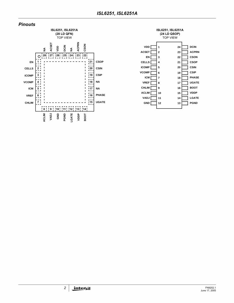
PinoutsISL6251, ISL6251A
(28 LD QFN)TOP VIEW
ISL6251, ISL6251A(24 LD QSOP)
TOP VIEW
1
2
3
4
5
6
7
21
20
19
18
17
16
15
28 27 26 25 24 23 22
8 9 10 11 12 13 14
EN
CELLS
ICOMP
VCOMP
ICM
VREF
CHLIM
AC
LIM
PG
ND
LGA
TE
VD
DP
BO
OT
CSOP
PHASE
UGATE
AC
SE
T
DC
IN
AC
PR
N
CS
ON
VA
DJ
GN
D
CSIN
CSIP
NA
NA
NA
VD
D
NA
DCIN 1 24VDD
2 23 ACPRN ACSET
3 22 CSON
4 21 CSOP
EN
5 20 CSIN
CELLS
6 19 CSIP
ICOMP
7 18
VCOMP
8 17
ICM
9 16
PHASE
VREF
10 15
UGATE
CHLIM
11 14
BOOT
ACLIM
12 13
VDDP
VADJ LGATE
GND PGND
2 FN9202.1June 17, 2005
ISL6251, ISL6251A
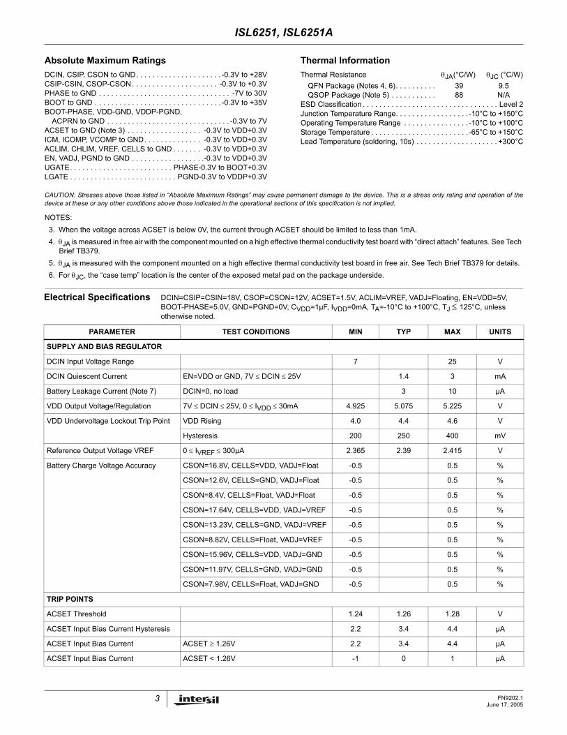
Absolute Maximum Ratings Thermal InformationDCIN, CSIP, CSON to GND. . . . . . . . . . . . . . . . . . . . . -0.3V to +28VCSIP-CSIN, CSOP-CSON. . . . . . . . . . . . . . . . . . . . . -0.3V to +0.3VPHASE to GND . . . . . . . . . . . . . . . . . . . . . . . . . . . . . . . . -7V to 30VBOOT to GND . . . . . . . . . . . . . . . . . . . . . . . . . . . . . . . -0.3V to +35VBOOT-PHASE, VDD-GND, VDDP-PGND,
ACPRN to GND . . . . . . . . . . . . . . . . . . . . . . . . . . . . . . -0.3V to 7VACSET to GND (Note 3) . . . . . . . . . . . . . . . . . . -0.3V to VDD+0.3VICM, ICOMP, VCOMP to GND. . . . . . . . . . . . . . -0.3V to VDD+0.3VACLIM, CHLIM, VREF, CELLS to GND . . . . . . . -0.3V to VDD+0.3VEN, VADJ, PGND to GND . . . . . . . . . . . . . . . . . .-0.3V to VDD+0.3VUGATE. . . . . . . . . . . . . . . . . . . . . . . . . PHASE-0.3V to BOOT+0.3VLGATE . . . . . . . . . . . . . . . . . . . . . . . . . . PGND-0.3V to VDDP+0.3V
Thermal Resistance θJA (°C/W) θJC (°C/W)QFN Package (Notes 4, 6). . . . . . . . . . 39 9.5QSOP Package (Note 5) . . . . . . . . . . . 88 N/A
ESD Classification . . . . . . . . . . . . . . . . . . . . . . . . . . . . . . . . . Level 2Junction Temperature Range. . . . . . . . . . . . . . . . . . -10°C to +150°COperating Temperature Range . . . . . . . . . . . . . . . . -10°C to +100°CStorage Temperature . . . . . . . . . . . . . . . . . . . . . . . . -65°C to +150°CLead Temperature (soldering, 10s) . . . . . . . . . . . . . . . . . . . . +300°C
CAUTION: Stresses above those listed in “Absolute Maximum Ratings” may cause permanent damage to the device. This is a stress only rating and operation of thedevice at these or any other conditions above those indicated in the operational sections of this specification is not implied.
NOTES:3. When the voltage across ACSET is below 0V, the current through ACSET should be limited to less than 1mA.4. θJA is measured in free air with the component mounted on a high effective thermal conductivity test board with “direct attach” features. See Tech
Brief TB379.5. θJA is measured with the component mounted on a high effective thermal conductivity test board in free air. See Tech Brief TB379 for details.6. For θJC, the “case temp” location is the center of the exposed metal pad on the package underside.
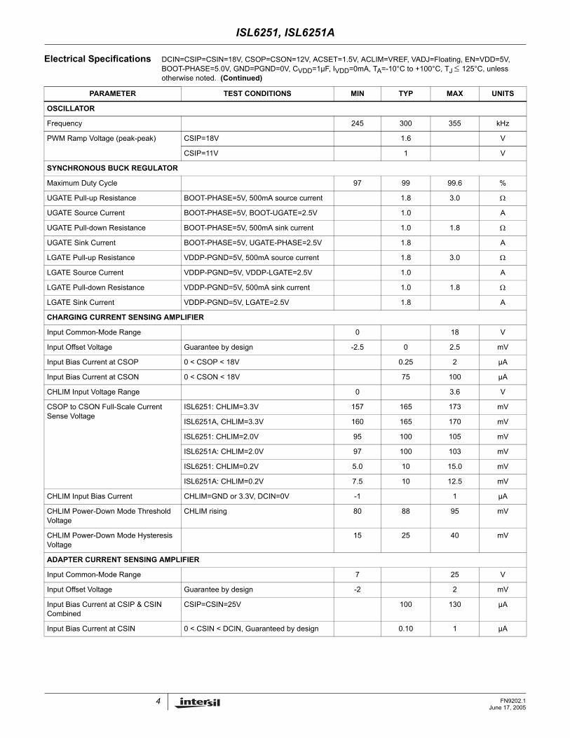
Electrical Specifications DCIN=CSIP=CSIN=18V, CSOP=CSON=12V, ACSET=1.5V, ACLIM=VREF, VADJ=Floating, EN=VDD=5V, BOOT-PHASE=5.0V, GND=PGND=0V, CVDD=1µF, IVDD=0mA, TA=-10°C to +100°C, TJ ≤ 125°C, unless otherwise noted.
PARAMETER TEST CONDITIONS MIN TYP MAX UNITS
SUPPLY AND BIAS REGULATOR
DCIN Input Voltage Range 7 25 V
DCIN Quiescent Current EN=VDD or GND, 7V ≤ DCIN ≤ 25V 1.4 3 mA
Battery Leakage Current (Note 7) DCIN=0, no load 3 10 µA
VDD Output Voltage/Regulation 7V ≤ DCIN ≤ 25V, 0 ≤ IVDD ≤ 30mA 4.925 5.075 5.225 V
VDD Undervoltage Lockout Trip Point VDD Rising 4.0 4.4 4.6 V
Hysteresis 200 250 400 mV
Reference Output Voltage VREF 0 ≤ IVREF ≤ 300µA 2.365 2.39 2.415 V
Battery Charge Voltage Accuracy CSON=16.8V, CELLS=VDD, VADJ=Float -0.5 0.5 %
CSON=12.6V, CELLS=GND, VADJ=Float -0.5 0.5 %
CSON=8.4V, CELLS=Float, VADJ=Float -0.5 0.5 %
CSON=17.64V, CELLS=VDD, VADJ=VREF -0.5 0.5 %
CSON=13.23V, CELLS=GND, VADJ=VREF -0.5 0.5 %
CSON=8.82V, CELLS=Float, VADJ=VREF -0.5 0.5 %
CSON=15.96V, CELLS=VDD, VADJ=GND -0.5 0.5 %
CSON=11.97V, CELLS=GND, VADJ=GND -0.5 0.5 %
CSON=7.98V, CELLS=Float, VADJ=GND -0.5 0.5 %
TRIP POINTS
ACSET Threshold 1.24 1.26 1.28 V
ACSET Input Bias Current Hysteresis 2.2 3.4 4.4 µA
ACSET Input Bias Current ACSET ≥ 1.26V 2.2 3.4 4.4 µA
ACSET Input Bias Current ACSET < 1.26V -1 0 1 µA
3 FN9202.1June 17, 2005
ISL6251, ISL6251A
OSCILLATOR
Frequency 245 300 355 kHz
PWM Ramp Voltage (peak-peak) CSIP=18V 1.6 V
CSIP=11V 1 V
SYNCHRONOUS BUCK REGULATOR
Maximum Duty Cycle 97 99 99.6 %
UGATE Pull-up Resistance BOOT-PHASE=5V, 500mA source current 1.8 3.0 Ω
UGATE Source Current BOOT-PHASE=5V, BOOT-UGATE=2.5V 1.0 A
UGATE Pull-down Resistance BOOT-PHASE=5V, 500mA sink current 1.0 1.8 Ω
UGATE Sink Current BOOT-PHASE=5V, UGATE-PHASE=2.5V 1.8 A
LGATE Pull-up Resistance VDDP-PGND=5V, 500mA source current 1.8 3.0 Ω
LGATE Source Current VDDP-PGND=5V, VDDP-LGATE=2.5V 1.0 A
LGATE Pull-down Resistance VDDP-PGND=5V, 500mA sink current 1.0 1.8 Ω
LGATE Sink Current VDDP-PGND=5V, LGATE=2.5V 1.8 A
CHARGING CURRENT SENSING AMPLIFIER
Input Common-Mode Range 0 18 V
Input Offset Voltage Guarantee by design -2.5 0 2.5 mV
Input Bias Current at CSOP 0 < CSOP < 18V 0.25 2 µA
Input Bias Current at CSON 0 < CSON < 18V 75 100 µA
CHLIM Input Voltage Range 0 3.6 V
CSOP to CSON Full-Scale Current Sense Voltage
ISL6251: CHLIM=3.3V 157 165 173 mV
ISL6251A, CHLIM=3.3V 160 165 170 mV
ISL6251: CHLIM=2.0V 95 100 105 mV
ISL6251A: CHLIM=2.0V 97 100 103 mV
ISL6251: CHLIM=0.2V 5.0 10 15.0 mV
ISL6251A: CHLIM=0.2V 7.5 10 12.5 mV
CHLIM Input Bias Current CHLIM=GND or 3.3V, DCIN=0V -1 1 µA
CHLIM Power-Down Mode Threshold Voltage
CHLIM rising 80 88 95 mV
CHLIM Power-Down Mode Hysteresis Voltage
15 25 40 mV
ADAPTER CURRENT SENSING AMPLIFIER
Input Common-Mode Range 7 25 V
Input Offset Voltage Guarantee by design -2 2 mV
Input Bias Current at CSIP & CSIN Combined
CSIP=CSIN=25V 100 130 µA
Input Bias Current at CSIN 0 < CSIN < DCIN, Guaranteed by design 0.10 1 µA
Electrical Specifications DCIN=CSIP=CSIN=18V, CSOP=CSON=12V, ACSET=1.5V, ACLIM=VREF, VADJ=Floating, EN=VDD=5V, BOOT-PHASE=5.0V, GND=PGND=0V, CVDD=1µF, IVDD=0mA, TA=-10°C to +100°C, TJ ≤ 125°C, unless otherwise noted. (Continued)
PARAMETER TEST CONDITIONS MIN TYP MAX UNITS
4 FN9202.1June 17, 2005
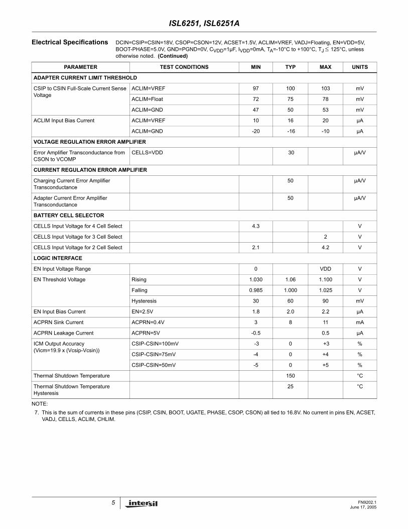
ISL6251, ISL6251A
ADAPTER CURRENT LIMIT THRESHOLD
CSIP to CSIN Full-Scale Current Sense Voltage
ACLIM=VREF 97 100 103 mV
ACLIM=Float 72 75 78 mV
ACLIM=GND 47 50 53 mV
ACLIM Input Bias Current ACLIM=VREF 10 16 20 µA
ACLIM=GND -20 -16 -10 µA
VOLTAGE REGULATION ERROR AMPLIFIER
Error Amplifier Transconductance from CSON to VCOMP
CELLS=VDD 30 µA/V
CURRENT REGULATION ERROR AMPLIFIER
Charging Current Error Amplifier Transconductance
50 µA/V
Adapter Current Error Amplifier Transconductance
50 µA/V
BATTERY CELL SELECTOR
CELLS Input Voltage for 4 Cell Select 4.3 V
CELLS Input Voltage for 3 Cell Select 2 V
CELLS Input Voltage for 2 Cell Select 2.1 4.2 V
LOGIC INTERFACE
EN Input Voltage Range 0 VDD V
EN Threshold Voltage Rising 1.030 1.06 1.100 V
Falling 0.985 1.000 1.025 V
Hysteresis 30 60 90 mV
EN Input Bias Current EN=2.5V 1.8 2.0 2.2 µA
ACPRN Sink Current ACPRN=0.4V 3 8 11 mA
ACPRN Leakage Current ACPRN=5V -0.5 0.5 µA
ICM Output Accuracy (Vicm=19.9 x (Vcsip-Vcsin))
CSIP-CSIN=100mV -3 0 +3 %
CSIP-CSIN=75mV -4 0 +4 %
CSIP-CSIN=50mV -5 0 +5 %
Thermal Shutdown Temperature 150 °C
Thermal Shutdown Temperature Hysteresis
25 °C
NOTE:7. This is the sum of currents in these pins (CSIP, CSIN, BOOT, UGATE, PHASE, CSOP, CSON) all tied to 16.8V. No current in pins EN, ACSET,
VADJ, CELLS, ACLIM, CHLIM.
Electrical Specifications DCIN=CSIP=CSIN=18V, CSOP=CSON=12V, ACSET=1.5V, ACLIM=VREF, VADJ=Floating, EN=VDD=5V, BOOT-PHASE=5.0V, GND=PGND=0V, CVDD=1µF, IVDD=0mA, TA=-10°C to +100°C, TJ ≤ 125°C, unless otherwise noted. (Continued)
PARAMETER TEST CONDITIONS MIN TYP MAX UNITS
5 FN9202.1June 17, 2005
ISL6251, ISL6251A
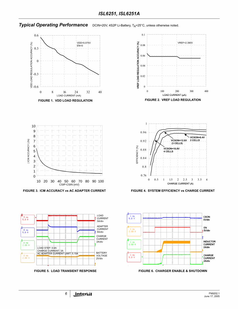
Typical Operating Performance DCIN=20V, 4S2P Li-Battery, TA=25°C, unless otherwise noted.
FIGURE 1. VDD LOAD REGULATION FIGURE 2. VREF LOAD REGULATION
FIGURE 3. ICM ACCURACY vs AC ADAPTER CURRENT FIGURE 4. SYSTEM EFFICIENCY vs CHARGE CURRENT
FIGURE 5. LOAD TRANSIENT RESPONSE FIGURE 6. CHARGER ENABLE & SHUTDOWN
-0.6
-0.3
0
0.3
0.6
0 8 16 24 32 40
VD
D L
OA
D R
EG
ULA
TIO
N A
CC
UR
AC
Y (%
) VDD=5.075VEN=0
LOAD CURRENT (mA)
-0.6
-0.3
0
0.3
0.6
0 8 16 24 32 40
VD
D L
OA
D R
EG
ULA
TIO
N A
CC
UR
AC
Y (%
) VDD=5.075VEN=0
LOAD CURRENT (mA)
0
0.02
0.04
0.06
0.08
0.1
0 100 200 300 400
VR
EF L
OA
D R
EG
ULA
TIO
N A
CC
UR
ACY
(%) VREF=2.390V
LOAD CURRENT (µA)
0
0.02
0.04
0.06
0.08
0.1
0 100 200 300 400
VR
EF L
OA
D R
EG
ULA
TIO
N A
CC
UR
ACY
(%) VREF=2.390V
LOAD CURRENT (µA)
CSIP-CSIN (mV)
0123456789
10
10 20 30 40 50 60 70 80 90 100
| IC
M A
CC
UR
AC
Y |
(%)
0.76
0.8
0.84
0.88
0.92
0.96
1
0 0.5 1 1.5 2 2.5 3 3.5 4
EFFI
CIE
NC
Y (%
)
CHARGE CURRENT (A)
VCSON=16.8V4 CELLS
VCSON=12.6V(3 CELLS)
VCSON=8.4V2 CELLS
0.76
0.8
0.84
0.88
0.92
0.96
1
0 0.5 1 1.5 2 2.5 3 3.5 4
EFFI
CIE
NC
Y (%
)
CHARGE CURRENT (A)
VCSON=16.8V4 CELLS
VCSON=12.6V(3 CELLS)
VCSON=8.4V2 CELLS
LOAD CURRENT5A/div
ADAPTERCURRENT5A/div
CHARGECURRENT2A/div
BATTERYVOLTAGE2V/div
LOAD STEP: 0-4A CHARGE CURRENT: 3A AC ADAPTER CURRENT LIMIT: 5.15A
CSON5V/div
EN5V/div
INDUCTORCURRENT2A/div
CHARGECURRENT2A/div
CSON5V/div
EN5V/div
INDUCTORCURRENT2A/div
CHARGECURRENT2A/div
6 FN9202.1June 17, 2005
ISL6251, ISL6251A
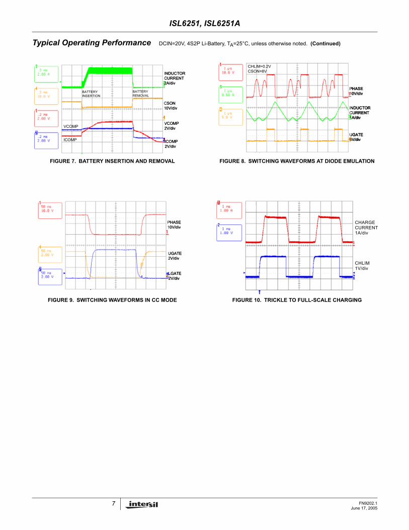
FIGURE 7. BATTERY INSERTION AND REMOVAL FIGURE 8. SWITCHING WAVEFORMS AT DIODE EMULATION
FIGURE 9. SWITCHING WAVEFORMS IN CC MODE FIGURE 10. TRICKLE TO FULL-SCALE CHARGING
Typical Operating Performance DCIN=20V, 4S2P Li-Battery, TA=25°C, unless otherwise noted. (Continued)
INDUCTORCURRENT2A/div
CSON10V/div
VCOMP
ICOMP
BATTERYINSERTION
BATTERYREMOVAL
VCOMP2V/div
ICOMP2V/div
INDUCTORCURRENT2A/div
CSON10V/div
VCOMP
ICOMP
BATTERYINSERTION
BATTERYREMOVAL
VCOMP2V/div
ICOMP2V/div
PHASE10V/div
INDUCTORCURRENT1A/div
UGATE5V/div
CHLIM=0.2VCSON=8V
PHASE10V/div
INDUCTORCURRENT1A/div
UGATE5V/div
PHASE10V/div
INDUCTORCURRENT1A/div
UGATE5V/div
CHLIM=0.2VCSON=8V
PHASE10V/div
LGATE2V/div
UGATE2V/div
PHASE10V/div
LGATE2V/div
UGATE2V/div
CHLIM 1V/div
CHARGE CURRENT1A/div
7 FN9202.1June 17, 2005
ISL6251, ISL6251A
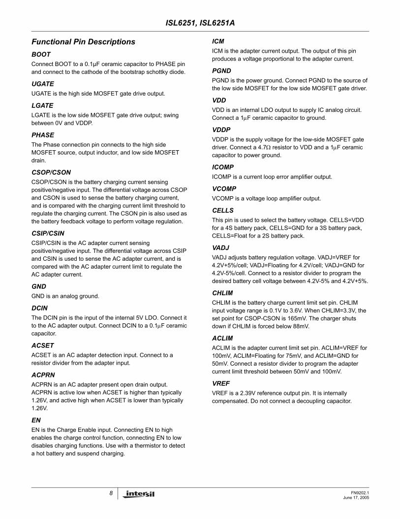
Functional Pin DescriptionsBOOTConnect BOOT to a 0.1µF ceramic capacitor to PHASE pin and connect to the cathode of the bootstrap schottky diode.
UGATEUGATE is the high side MOSFET gate drive output.
LGATELGATE is the low side MOSFET gate drive output; swing between 0V and VDDP.
PHASEThe Phase connection pin connects to the high side MOSFET source, output inductor, and low side MOSFET drain.
CSOP/CSONCSOP/CSON is the battery charging current sensing positive/negative input. The differential voltage across CSOP and CSON is used to sense the battery charging current, and is compared with the charging current limit threshold to regulate the charging current. The CSON pin is also used as the battery feedback voltage to perform voltage regulation.
CSIP/CSINCSIP/CSIN is the AC adapter current sensing positive/negative input. The differential voltage across CSIP and CSIN is used to sense the AC adapter current, and is compared with the AC adapter current limit to regulate the AC adapter current.
GNDGND is an analog ground.
DCINThe DCIN pin is the input of the internal 5V LDO. Connect it to the AC adapter output. Connect DCIN to a 0.1µF ceramic capacitor.
ACSETACSET is an AC adapter detection input. Connect to a resistor divider from the adapter input.
ACPRNACPRN is an AC adapter present open drain output. ACPRN is active low when ACSET is higher than typically 1.26V, and active high when ACSET is lower than typically 1.26V.
ENEN is the Charge Enable input. Connecting EN to high enables the charge control function, connecting EN to low disables charging functions. Use with a thermistor to detect a hot battery and suspend charging.
ICMICM is the adapter current output. The output of this pin produces a voltage proportional to the adapter current.
PGNDPGND is the power ground. Connect PGND to the source of the low side MOSFET for the low side MOSFET gate driver.
VDDVDD is an internal LDO output to supply IC analog circuit. Connect a 1µF ceramic capacitor to ground.
VDDPVDDP is the supply voltage for the low-side MOSFET gate driver. Connect a 4.7Ω resistor to VDD and a 1µF ceramic capacitor to power ground.
ICOMPICOMP is a current loop error amplifier output.
VCOMPVCOMP is a voltage loop amplifier output.
CELLSThis pin is used to select the battery voltage. CELLS=VDD for a 4S battery pack, CELLS=GND for a 3S battery pack, CELLS=Float for a 2S battery pack.
VADJVADJ adjusts battery regulation voltage. VADJ=VREF for 4.2V+5%/cell; VADJ=Floating for 4.2V/cell; VADJ=GND for 4.2V-5%/cell. Connect to a resistor divider to program the desired battery cell voltage between 4.2V-5% and 4.2V+5%.
CHLIMCHLIM is the battery charge current limit set pin. CHLIM input voltage range is 0.1V to 3.6V. When CHLIM=3.3V, the set point for CSOP-CSON is 165mV. The charger shuts down if CHLIM is forced below 88mV.
ACLIMACLIM is the adapter current limit set pin. ACLIM=VREF for 100mV, ACLIM=Floating for 75mV, and ACLIM=GND for 50mV. Connect a resistor divider to program the adapter current limit threshold between 50mV and 100mV.
VREFVREF is a 2.39V reference output pin. It is internally compensated. Do not connect a decoupling capacitor.
8 FN9202.1June 17, 2005
ISL6251, ISL6251A
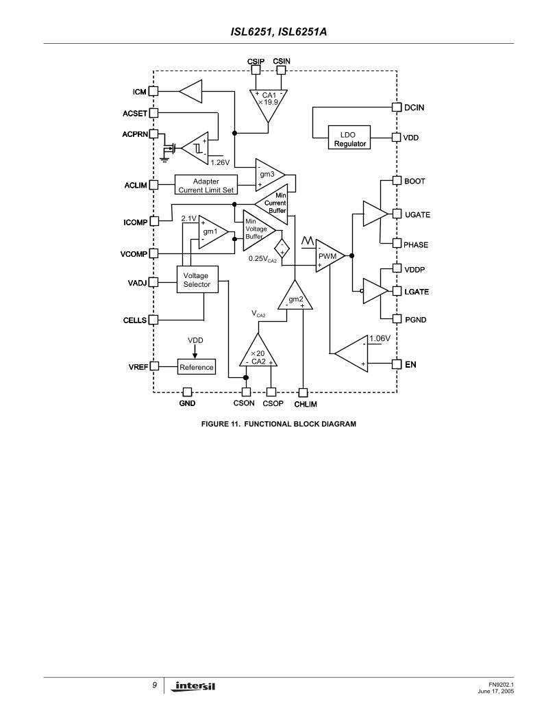
FIGURE 11. FUNCTIONAL BLOCK DIAGRAM
CHLIMCSON CSOP
+
-
BOOT
ACPRN
VDDP
CELLS
VADJ
GND
VCOMP
ACSET
+
-
ACLIM
1.27V
2.1VICOMP
CSINCSIP
+ICM
+
-
gm2
gm3
CA2
gm1
CA1
VoltageSelector
LDO Regulator
PHASE
VDDP
LGATE
Adapter Current Limit Set
0.25 VCA2
UGATE
PWM+
-
ReferenceVREF
MinVoltageBuffer
VDD
VCA2
+
+
-EN
1.065V
+
-
MinCurrent
Buffer
+-
+
-
ACPRN
CELLS
VADJ
GND
VCOMP
ACSET
+
ACLIM
1.26V
CHLIM
ICOMP
CSINCSIP
ICM
+
-
gm2
gm3
VoltageSelector
RegulatorLDO
Regulator
LGATE
PGND
0.25VCA2PWM+
-PWM+
-
ReferenceVREF
MinVoltageBuffer
MinVoltageBuffer
VDD
VCA2
VDD
EN
1.06V
+
-
+-
DCINCA1
×19.9
CA2 +×20
AdapterCurrent Limit Set
MinCurrent
Buffer
gm1
2.1V
-
-
-
+-
+
CHLIMCSON CSOP
+
-
BOOT
ACPRN
VDDP
CELLS
VADJ
GND
VCOMP
ACSET
+
-
+
-
ACLIM
1.27V
2.1VICOMP
CSINCSIP
+ICM
+
-
gm2
gm3
CA2
gm1
CA1
VoltageSelector
LDO Regulator
LDO Regulator
PHASE
VDDP
LGATE
Adapter Current Limit Set
0.25 VCA2
UGATE
PWM+
-PWM+
-
ReferenceVREF
MinVoltageBuffer
MinVoltageBuffer
VDD
VCA2
++
+
-EN
1.065V
+
-
MinCurrent
Buffer
MinCurrent
Buffer
+-
+
-
ACPRN
CELLS
VADJ
GND
VCOMP
ACSET
+
ACLIM
1.26V
CHLIM
ICOMP
CSINCSIP
ICM
+
-
gm2
gm3
VoltageSelector
RegulatorLDO
Regulator
LGATE
PGND
0.25VCA2PWM+
-PWM+
-
ReferenceVREF
MinVoltageBuffer
MinVoltageBuffer
VDD
VCA2
VDD
EN
1.06V
+
-
+-
DCINCA1
×19.9
CA2 +×20
AdapterCurrent Limit Set
MinCurrent
Buffer
MinCurrent
Buffer
gm1
2.1V
-
-
-
+-
+
9 FN9202.1June 17, 2005
ISL6251, ISL6251A
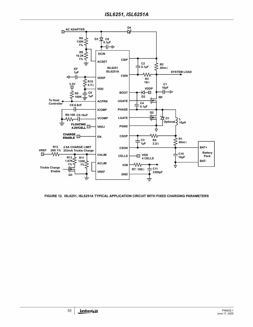
FIGURE 12. ISL6251, ISL6251A TYPICAL APPLICATION CIRCUIT WITH FIXED CHARGING PARAMETERS
CSIP
CSIN
BOOT
UGATE
PHASE
LGATE
PGND
CSOP
CSON
CELLS
ICM
GND
DCIN
ACSET
VDDP
VDD
ACPRN
ICOMP
VCOMP
VADJ
EN
CHLIM
ACLIM
VREF
Q1
Q2
L10µH
C110µF
SYSTEM LOAD
C1010µF
R140mΩ
AC ADAPTER
R220mΩ
R318Ω
R42.2Ω
R6:10K
R5100K
R8130K
1%
R910.2K
1%C20.1µF
C40.1µF
C31µF
C5:10nF
C6:6.8nF
C91µF
ISL6251
ISL6251A
FLOATING4.2V/CELL
R104.7Ω
C7 1µF
3.3V
BatteryPack
BAT+
BAT-
VDD4 CELLS
D1Optional
D2
VDDP
VREFR12
20K 1%
R11130K
1%
R131.87K
1%
2.6A CHARGE LIMIT253mA Trickle Charge
C113300pF
Q3
Trickle ChargeEnable
D4
To HostController
CHARGEENABLE
CSIP
CSIN
BOOT
UGATE
PHASE
LGATE
PGND
CSOP
CSON
CELLS
ICM
GND
DCIN
ACSET
VDDP
VDD
ACPRN
ICOMP
VCOMP
VADJ
EN
CHLIM
ACLIM
VREF
Q1
C80.1µF
ISL6251ISL6251A
FLOATING4.2V/CELL
C7
D3
R7: 100Ω
CHARGEENABLE
10 FN9202.1June 17, 2005
ISL6251, ISL6251A
DCIN
ACSET
VDDP
VDD
ACPRN
CHLIM
EN
ICM
ACLIM
VREF
ICOMP
VCOMP
VADJ
Q1
Q2 L10µH
C110µF
C1010µF
R140mΩ
AC ADAPTER
R220mΩ
R42.2Ω
R5100K
R8130K
1%R9
10.2K,1%
C20.1µF
C40.1µF
C31µF
6.8nF
C91µF
C80.1µF
ISL6251
ISL6251A
C510nF
FLOATING4.2V/CELL
R610K
C71µF
R104.7Ω
BatteryPack
BAT+
SCLSDLTEMPBAT-
SCLSDL
A/D INPUTGND
5.15A INPUT CURRENT LIMIT
3 CELLS
HOST
R11, R12, R1310k
D1Optional
VDDP
D2
D3
R7: 100Ω
CSIP
CSIN
BOOT
UGATE
PHASE
LGATE
PGND
CSOP
CSON
CELLS
GND
C113300pF
D4
SYSTEM LOAD
DCIN
ACSET
VDDP
VDD
ACPRN
CHLIM
EN
ICM
ACLIM
VREF
ICOMP
VCOMP
VADJ
R3: 18Ω
C6
ISL6251
ISL6251A
BatteryPack
BAT+
SCLSDLTEMPBAT-
BatteryPack
BAT+
SCLSDLTEMPBAT-
VCC
OUTPUT
D/A OUTPUT
A/D INPUT
DIGITALINPUT
AVDD/VREF
CSIP
CSIN
BOOT
UGATE
PHASE
LGATE
PGND
CSOP
CSON
CELLS
GND
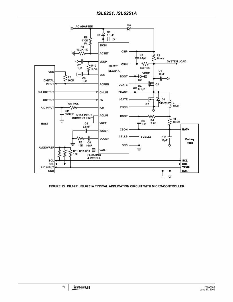
FIGURE 13. ISL6251, ISL6251A TYPICAL APPLICATION CIRCUIT WITH MICRO-CONTROLLER
11 FN9202.1June 17, 2005
ISL6251, ISL6251A
Theory of OperationIntroductionThe ISL6251, ISL6251A includes all of the functions necessary to charge 2 to 4 cell Li-Ion and Li-polymer batteries. A high efficiency synchronous buck converter is used to control the charging voltage and charging current up to 10A. The ISL6251, ISL6251A has input current limiting and analog inputs for setting the charge current and charge voltage; CHLIM inputs are used to control charge current and VADJ inputs are used to control charge voltage.
The ISL6251, ISL6251A charges the battery with constant charge current, set by CHLIM input, until the battery voltage rises up to a programmed charge voltage set by VADJ input; then the charger begins to operate at a constant voltage charge mode.
The EN input allows shutdown of the charger through a command from a micro-controller. It also uses EN to safely shutdown the charger when the battery is in extremely hot conditions. The amount of adapter current is reported on the ICM output. Figure 11 shows the IC functional block diagram.
The synchronous buck converter uses external N-channel MOSFETs to convert the input voltage to the required charging current and charging voltage. Figure 12 shows the ISL6251, ISL6251A typical application circuit with charging current and charging voltage fixed at specific values. The typical application circuit shown in Figure 13 shows the ISL6251, ISL6251A typical application circuit which uses a micro-controller to adjust the charging current set by CHLIM input. The voltage at CHLIM and the value of R1 sets the charging current. The DC/DC converter generates the control signals to drive two external N-channel MOSFETs to regulate the voltage and current set by the ACLIM, CHLIM, VADJ and CELLS inputs.
The ISL6251, ISL6251A features a voltage regulation loop (VCOMP) and two current regulation loops (ICOMP). The VCOMP voltage regulation loop monitors CSON to ensure that its voltage never exceeds the voltage and regulates the battery charge voltage set by VADJ. The ICOMP current regulation loops regulate the battery charging current delivered to the battery to ensure that it never exceeds the charging current limit set by CHLIM; and the ICOMP current regulation loops also regulate the input current drawn from the AC adapter to ensure that it never exceeds the input current limit set by ACLIM, and to prevent a system crash and AC adapter overload.
PWM ControlThe ISL6251, ISL6251A employs a fixed frequency PWM current mode control architecture with a feed forward function. The feed-forward function maintains a constant modulator gain of 11 to achieve fast line regulation as the buck input voltage changes. When the battery charge
voltage approaches the input voltage, the DC/DC converter operates in dropout mode, where there is a timer to prevent the frequency from dropping into the audible frequency range. It can achieve duty cycle of up to 99.6%.
To prevent boosting of the system bus voltage, the battery charger operates in standard-buck mode when CSOP-CSON drops below 4.25mV. Once in standard-buck mode, hysteresis does not allow synchronous operation of the DC/DC converter until CSOP-CSON rises above 12.5mV.
An adaptive gate drive scheme is used to control the dead time between two switches. The dead time control circuit monitors the LGATE output and prevents the upper side MOSFET from turning on until LGATE is fully off, preventing cross-conduction and shoot-through. In order for the dead time circuit to work properly, there must be a low resistance, low inductance path from the LGATE driver to MOSFET gate, and from the source of MOSFET to PGND. The external Schottky diode is between the VDDP pin and BOOT pin to keep the bootstrap capacitor charged.
Setting the Battery Regulation VoltageThe ISL6251, ISL6251A uses a high-accuracy trimmed band-gap voltage reference to regulate the battery charging voltage. The VADJ input adjusts the charger output voltage, and the VADJ control voltage can vary from 0 to VREF, providing a 10% adjustment range (from 4.2V-5% to 4.2V+5%) on CSON regulation voltage. An overall voltage accuracy of better than 0.5% is achieved.
The per-cell battery termination voltage is a function of the battery chemistry. Consult the battery manufacturers to determine this voltage.
• Float VADJ to set the battery voltage VCSON=4.2V × number of the cells,
• Connect VADJ to VREF to set 4.41V × number of cells,
• Connect VADJ to ground to set 3.99V × number of the cells.
So, the maximum battery voltage of 17.6V can be achieved. Note that other battery charge voltages can be set by connecting a resistor divider from VREF to ground. The resistor divider should be sized to draw no more than 100µA from VREF; or connect a low impedance voltage source like the D/A converter in the micro-controller. The programmed battery voltage per cell can be determined by the following equation:
Connect CELLS as shown in Table 1 to charge 2, 3 or 4 Li+ cells. When charging other cell chemistries, use CELLS to select an output voltage range for the charger. The internal error amplifier gm1 maintains voltage regulation. The voltage error amplifier is compensated at VCOMP. The component values shown in Figure 12 provide suitable performance for most applications. Individual compensation of the voltage
V 3.99V 175.0V VADJCELL +=
12 FN9202.1June 17, 2005
ISL6251, ISL6251A
regulation and current-regulation loops allows for optimal compensation.
Setting the Battery Charge Current LimitThe CHLIM input sets the maximum charging current. The current set by the current sense-resistor connects between CSOP and CSON. The full-scale differential voltage between CSOP and CSON is 165mV for CHLIM=3.3V, so the maximum charging current is 4.125A for a 40mΩ sensing resistor. Other battery charge current-sense threshold values can be set by connecting a resistor divider from VREF or 3.3V to ground, or by connecting a low impedance voltage source like a D/A converter in the micro-controller. The charge current limit threshold is given by:
To set the trickle charge current for the dumb charger, a resistor in series with a switch Q3 (Figure 12) controlled by the micro-controller is connected from CHLIM pin to ground. The trickle charge current is determined by:
When the CHLIM voltage is below 88mV (typical), it will disable the battery charger. When choosing the current sensing resistor, note that the voltage drop across the sensing resistor causes further power dissipation, reducing efficiency. However, adjusting CHLIM voltage to reduce the voltage across the current sense resistor R1 will degrade accuracy due to the smaller signal to the input of the current sense amplifier. There is a trade-off between accuracy and power dissipation. A low pass filter is recommended to eliminate switching noise. Connect the resistor to the CSOP pin instead of the CSON pin, as the CSOP pin has lower bias current and less influence on current-sense accuracy and voltage regulation accuracy.
Setting the Input Current LimitThe total input current from an AC adapter, or other DC source, is a function of the system supply current and the battery-charging current. The input current regulator limits the input current by reducing the charging current, when the input current exceeds the input current limit set point. System current normally fluctuates as portions of the system are powered up or down. Without input current regulation, the source must be able to supply the maximum system
current and the maximum charger input current simultaneously. By using the input current limiter, the current capability of the AC adapter can be lowered, reducing system cost.
The ISL6251, ISL6251A limits the battery charge current when the input current-limit threshold is exceeded, ensuring the battery charger does not load down the AC adapter voltage. This constant input current regulation allows the adapter to fully power the system and prevent the AC adapter from overloading and crashing the system bus.
An internal amplifier gm3 compares the voltage between CSIP and CSIN to the input current limit threshold voltage set by ACLIM. Connect ACLIM to REF, Float and GND for the full-scale input current limit threshold voltage of 100mV, 75mV and 50mV, respectively, or use a resistor divider from VREF to ground to set the input current limit as the following equation:
When choosing the current sense resistor, note that the voltage drop across this resistor causes further power dissipation, reducing efficiency. The AC adapter current sense accuracy is very important. Use a 1% tolerance current-sense resistor. The highest accuracy of ±3% is achieved with 100mV current-sense threshold voltage for ACLIM=VREF, but it has the highest power dissipation. For example, it has 400mW power dissipation for rated 4A AC adapter and 1W sensing resistor may have to be used. ±4% and ±6% accuracy can be achieved with 75mV and 50mV current-sense threshold voltage for ACLIM=Floating and ACLIM=GND, respectively.
A low pass filter is suggested to eliminate the switching noise. Connect the resistor to CSIN pin instead of CSIP pin because CSIN pin has lower bias current and less influence on the current-sense accuracy.
AC Adapter DetectionConnect the AC adapter voltage through a resistor divider to ACSET to detect when AC power is available, as shown in Figure 12. ACPRN is an open-drain output and is high when ACSET is less than Vth,rise, and active low when ACSET is above Vth,fall. Vth,rise and Vth,fall are given by:
Where Ihys is the ACSET input bias current hysteresis and VACSET = 1.24V (min), 1.26V (typ.) and 1.28V (max.). The hysteresis is IhysR8, where Ihys=2.2µA (min.), 3.4µA (typ.) and 4.4µA (max.).
TABLE 1. CELL NUMBER PROGRAMMING
CELLS CELL NUMBER
VDD 4
GND 3
Float 2
ICHG165mV
R1-------------------
VCHLIM3.3V
----------------------=
ICHG165mV
R1-------------------
VCHLIM trickle,3.3V
----------------------------------------=
+= 050.0VVREF
05.0R1I ACLIM2
INPUT
ACSET98
rise,th V1RRV •
+=
8hysACSET98
fall,th RIV1RR
V −•
+=
13 FN9202.1June 17, 2005
ISL6251, ISL6251A
Current MeasurementUse ICM to monitor the input current being sensed across CSIP and CSIN. The output voltage range is 0 to 2.5V. The voltage of ICM is proportional to the voltage drop across CSIP and CSIN, and is given by the following equation:
where IINPUT is the DC current drawn from the AC adapter. ICM has ±3% accuracy.
A low pass filter connected to ICM output is used to filter the switching noise.
LDO RegulatorVDD provides a 5.075V supply voltage from the internal LDO regulator from DCIN and can deliver up to 30mA of current. The MOSFET drivers are powered by VDDP, which must be connected to VDDP as shown in Figure 12. VDDP connects to VDD through an external resistor. Bypass VDDP and VDD with a 1µF capacitor.
ShutdownThe ISL6251, ISL6251A features a low-power shutdown mode. Driving EN low shuts down the charger. In shutdown, the DC/DC converter is disabled, and VCOMP and ICOMP are pulled to ground. The ICM, ACPRN outputs continue to function.
EN can be driven by a thermistor to allow automatic shutdown when the battery pack is hot. Often a NTC thermistor is included inside the battery pack to measure its temperature. When connected to the charger, the thermistor forms a voltage divider with a resistive pull-up to the VREF. The threshold voltage of EN is 1.06V with 60mV hysteresis. The thermistor can be selected to have a resistance vs temperature characteristic that abruptly decreases above a critical temperature. This arrangement automatically shuts down the charger when the battery pack is above a critical temperature.
Another method for inhibiting charging is to force CHLIM below 88mV (Typ.).
Short Circuit Protection and 0V Battery ChargingSince the battery charger will regulate the charge current to the limit set by CHLIM, it automatically has short circuit protection and is able to provide the charge current to wake up an extremely discharged battery.
Over Temperature ProtectionIf the die temp exceeds 150°C, it stops charging. Once the die temp drops below 125°C, charging will start up again.
Application InformationThe following battery charger design refers to the typical application circuit in Figure 12, where typical battery configuration of 4S2P is used. This section describes how to select the external components including the inductor, input and output capacitors, switching MOSFETs, and current sensing resistors.
Inductor SelectionThe inductor selection has trade-offs between cost, size and efficiency. For example, the lower the inductance, the smaller the size, but ripple current is higher. This also results in higher AC losses in the magnetic core and the windings, which decrease the system efficiency. On the other hand, the higher inductance results in lower ripple current and smaller output filter capacitors, but it has higher DCR (DC resistance of the inductor) loss, and has slower transient response. So, the practical inductor design is based on the inductor ripple current being ±(15-20)% of the maximum operating DC current at maximum input voltage. The required inductance can be calculated from:
Where VIN,MAX, VBAT, and fs are the maximum input voltage, battery voltage and switching frequency, respectively. The inductor ripple current ∆I is found from:
where the maximum peak-to-peak ripple current is 30% of the maximum charge current is used.
For VIN,MAX=19V, VBAT=16.8V, IBAT,MAX=2.6A, and fs=300kHz, the calculated inductance is 8.3µH. Choosing the closest standard value gives L=10µH. Ferrite cores are often the best choice since they are optimized at 300kHz to 600kHz operation with low core loss. The core must be large enough not to saturate at the peak inductor current IPeak:
Output Capacitor SelectionThe output capacitor in parallel with the battery is used to absorb the high frequency switching ripple current and smooth the output voltage. The RMS value of the output ripple current Irms is given by:
where the duty cycle D is the ratio of the output voltage (battery voltage) over the input voltage for continuous conduction mode which is typical operation for the battery charger. During the battery charge period, the output voltage varies from its initial battery voltage to the rated battery voltage. So, the duty cycle change can be in the range of
ICM 19.9 IINPUT R2••=
sMAX,IN
BAT
L
BATMAX,INf V
VI
VVL
∆−
=
MAXBAT,L I30%I ⋅=∆
LMAX,BATPeak I 21II ∆+=
( )D1 Df L 12
VI
s
MAX,INRMS −=
14 FN9202.1June 17, 2005
s
ISL6251, ISL6251A
between 0.53 and 0.88 for the minimum battery voltage of 10V (2.5V/Cell) and the maximum battery voltage of 16.8V.
For VIN,MAX=19V, VBAT=16.8V, L=10µH, and fs=300kHz, the maximum RMS current is 0.19A. A typical 10F ceramic capacitor is a good choice to absorb this current and also has very small size. The tantalum capacitor has a known failure mechanism when subjected to high surge current.
EMI considerations usually make it desirable to minimize ripple current in the battery leads. Beads may be added in series with the battery pack to increase the battery impedance at 300kHz switching frequency. Switching ripple current splits between the battery and the output capacitor depending on the ESR of the output capacitor and battery impedance. If the ESR of the output capacitor is 10mΩ and battery impedance is raised to 2Ω with a bead, then only 0.5% of the ripple current will flow in the battery.
MOSFET SelectionThe Notebook battery charger synchronous buck converter has the input voltage from the AC adapter output. The maximum AC adapter output voltage does not exceed 25V. Therefore, 30V logic MOSFET should be used.
The high side MOSFET must be able to dissipate the conduction losses plus the switching losses. For the battery charger application, the input voltage of the synchronous buck converter is equal to the AC adapter output voltage, which is relatively constant. The maximum efficiency is achieved by selecting a high side MOSFET that has the conduction losses equal to the switching losses. Ensure that ISL6251 LGATE gate driver can supply sufficient gate current to prevent it from conduction, which is due to the injected current into the drain-to-source parasitic capacitor (Miller capacitor Cgd), and caused by the voltage rising rate at phase node at the time instant of the high-side MOSFET turning on; otherwise, cross-conduction problems may occur. Reasonably slowing turn-on speed of the high-side MOSFET by connecting a resistor between the BOOT pin and gate drive supply source, and the high sink current capability of the low-side MOSFET gate driver help reduce the possibility of cross-conduction.
For the high-side MOSFET, the worst-case conduction losses occur at the minimum input voltage:
The optimum efficiency occurs when the switching losses equal the conduction losses. However, it is difficult to calculate the switching losses in the high-side MOSFET since it must allow for difficult-to-quantify factors that influence the turn-on and turn-off times. These factors include the MOSFET internal gate resistance, gate charge, threshold voltage, stray inductance, pull-up and pull-down
resistance of the gate driver. The following switching loss calculation provides a rough estimate.
Where Qgd: drain-to-gate charge, Qrr: total reverse recovery charge of the body-diode in low side MOSFET, ILV: inductor valley current, ILP: Inductor peak current, Ig,sink and Ig,source are the peak gate-drive source/sink current of Q1, respectively.
To achieve low switching losses, it requires low drain-to-gate charge Qgd. Generally, the lower the drain-to-gate charge, the higher the on-resistance. Therefore, there is a trade-off between the on-resistance and drain-to-gate charge. Good MOSFET selection is based on the Figure of Merit (FOM), which is a product of the total gate charge and on-resistance. Usually, the smaller the value of FOM, the higher the efficiency for the same application.
For the low-side MOSFET, the worst-case power dissipation occurs at minimum battery voltage and maximum input voltage:
Choose a low-side MOSFET that has the lowest possible on-resistance with a moderate-sized package like the SO-8 and is reasonably priced. The switching losses are not an issue for the low side MOSFET because it operates at zero-voltage-switching.
Choose a Schottky diode in parallel with low-side MOSFET Q2 with a forward voltage drop low enough to prevent the low-side MOSFET Q2 body-diode from turning on during the dead time. This also reduces the power loss in the high-side MOSFET associated with the reverse recovery of the low-side MOSFET Q2 body diode.
As a general rule, select a diode with DC current rating equal to one-third of the load current. One option is to choose a combined MOSFET with the Schottky diode in a single package. The integrated packages may work better in practice because there is less stray inductance due to a short connection. This Schottky diode is optional and may be removed if efficiency loss can be tolerated. In addition, ensure that the required total gate drive current for the selected MOSFETs should be less than 24mA. So, the total gate charge for the high-side and low-side MOSFETs is limited by the following equation:
Where IGATE is the total gate drive current and should be less than 24mA. Substituting IGATE=24mA and fs=300kHz into the above equation yields that the total gate charge
DSON2BAT
IN
OUTConduction,1Q RI
VV
P =
INrrksin,g
gdsLPIN
source,g
gdsLVINSwitching,1Q fVQ
IQ
f IV21
IQ
f IV21P ++=
DSON2BAT
IN
OUT2Q RI
VV
1P
−=
s
GATEGATE f
IQ ≤
15 FN9202.1June 17, 2005
ISL6251, ISL6251A
should be less than 80nC. Therefore, the ISL6251 easily drives the battery charge current up to 10A.
Input Capacitor SelectionThe input capacitor absorbs the ripple current from the synchronous buck converter, which is given by:
This RMS ripple current must be smaller than the rated RMS current in the capacitor datasheet. Non-tantalum chemistries (ceramic, aluminum, or OSCON) are preferred due to their resistance to power-up surge currents when the AC adapter is plugged into the battery charger. For Notebook battery charger applications, it is recommend that ceramic capacitors or polymer capacitors from Sanyo be used due to their small size and reasonable cost.
Table 2 shows the component lists for the typical application circuit in Figure 12.
Loop Compensation DesignISL6251 uses constant frequency current mode control architecture to achieve fast loop transient response. Accurate current sensing resistors in series with the output inductor is used to regulate the charge current, and the sensed current signal is injected into the voltage loop to achieve current mode control to simplify the loop compensation design. The inductor is not considered as a state variable for current mode control and the system becomes single order system. It is much easier to design a compensator to stabilize the voltage loop than voltage mode control. Figure 14 shows the small signal model of the synchronous buck regulator.
PWM Comparator Gain Fm:The PWM comparator gain Fm for peak current mode control is given by:
Where VPWM is the peak-peak voltage of the PWM ramp signal.
Current Sampling Transfer Function He(S):In current loop, the current signal is sampled every switching cycle. It has the following transfer function:
where Qn and ωn are given by ωn=π fs, respectively.
Power Stage Transfer FunctionsTransfer function F1(S) from control to output voltage is:
Where ,
Transfer function F2(S) from control to inductor current is:
, where .
Current loop gain Ti(S) is expressed as the following equation:
where RT is the trans-resistance in current loop. RT is usually equal to the product of the current sensing resistance of the current amplifier. For ISL6251, RT=20R1.
TABLE 2. COMPONENT LIST
PARTS PART NUMBERS AND MANUFACTURER
C1, C10 10µF/25V ceramic capacitor, Taiyo Yuden TMK325 MJ106MY X5R (3.2x2.5x1.9mm)
C2, C4, C8 0.1µF/50V ceramic capacitor
C3, C7, C9 1µF/10V ceramic capacitor, Taiyo Yuden LMK212BJ105MG
C5 10nF ceramic capacitor
C6 6.8nF ceramic capacitor
C11 3300pF ceramic capacitor
D1 30V/3A Schottky diode, EC31QS03L (optional)
D2, D3 100mA/30V Schottky Diode, Central Semiconductor
D4 8A/30V Schottky rectifier, STPS8L30B (optional)
L 10µH/3.8A/26mΩ, Sumida, CDRH104R-100
Q1, Q2 30V/35mΩ, FDS6912A, Fairchild.
Q3 Signal N-channel MOSFET, 2N7002
R1 40mΩ, ±1%, LRC-LR2512-01-R040-F, IRC
R2 20mΩ, ±1%, LRC-LR2010-01-R020-F, IRC
R3 18Ω, ±5%, (0805)
R4 2.2Ω, ±5%, (0805)
R5 100kΩ, ±5%, (0805)
R6 10k, ±5%, (0805)
R7 100Ω, ±5%, (0805)
R8, R11 130k, ±1%, (0805)
R9 10.2kΩ, ±1%, (0805)
R10 4.7Ω, ±5%, (0805)
R12 20kΩ, ±1%, (0805)
R13 1.87kΩ, ±1%, (0805)
( )IN
OUTINOUTBATrms V
VVVII
−=
PWMcompm V
1v
dF ==
( ) 1QSSSH
nn2n
2e ++=
ωω
,2Qn π−=
( )1
QSS
S1V
dv
SF
po2o
2esr
ino
1++
+==
ωω
ω
,CR1
ocesr =ω
LC
RQ oop ≈
oo
LC1
=ω
( )1
QSS
S1
RRV
di
SF
po2o
2z
LoinL
2++
+
+==
ωω
ω
ooz CR
1≈ω
( ) ( )SHSFFR)S(T e2mTi =
16 FN9202.1June 17, 2005
ISL6251, ISL6251A
The voltage gain with open current loop is:
Where , VFB is the feedback voltage of the voltage
error amplifier. The Voltage loop gain with current loop
closed is given by:
If Ti(S)>>1, then it can be simplified as follows:
,
From the above equation, it is shown that the system is a single order system, which has a single pole located at before the half switching frequency. Therefore, simple type II compensator can be easily used to stabilize the system.
Figure 15 shows the voltage loop compensator, and its transfer function is expressed as follows:
FIGURE 14. SMALL SIGNAL MODEL OF SYNCHRONOUS BUCK REGULATOR
FIGURE 15. VOLTAGE LOOP COMPENSATOR
where
Compensator design goal:
• High DC gain
• Loop bandwidth fc:
• Gain margin: >10dB
• Phase margin: 40°
The compensator design procedure is as follows:
1. Put compensator zero at:
2. Put one compensator pole at zero frequency to achieve high DC gain, and put another compensator pole at either ESR zero frequency or half switching frequency, whichever is lower.
The loop gain Tv(S) at cross over frequency of fc has unity gain. Therefore, the compensator resistance R1 is determined by:
where gm is the trans-conductance of the voltage loop error amplifier. Compensator capacitor C1 is then given by:
Example: Vin=19V, Vo=16.8V, Io=2.6A, fs=300kHz, Co=10µF/10mΩ, L=10µH, gm=250µs, RT=0.2Ω, VFB=2.1V, VPWM=VIN/11, fc=20kHz, then compensator resistance R1=8.0kΩ. Choose R1=10kΩ. Put the compensator zero at 1.5kHz. The compensator capacitor is C1=10nF. Therefore, choose voltage loop compensator: R1=10K, C1=10nF.
PCB Layout ConsiderationsPower and Signal Layers Placement on the PCBAs a general rule, power layers should be close together, either on the top or bottom of the board, with signal layers on the opposite side of the board. As an example, layer arrangement on a 4-layer board is shown below:
1. Top Layer: signal lines, or half board for signal lines and the other half board for power lines
2. Signal Ground 3. Power Layers: Power Ground4. Bottom Layer: Power MOSFET, Inductors and other
Power tracesSeparate the power voltage and current flowing path from the control and logic level signal path. The controller IC will
( ) ( )SASFKF)S(T v1mv =
oFB
VVK =
( )( )ST1
ST)S(Li
vv +
=
( )( )SHSA
S1
S1
RRR
VV
)S(Lev
p
esr
T
Lo
oFB
v
ω
ω
+
++
=oo
p CR1
≈ω
pω
dVindILinv
ini L
+
1:D
+ Li
Co
RcRo
-Av(S)
d
compv
RT
Fm
He(S)+
Ti(S)K
ov
Tv(S)
dVindILinv
ini L
+
1:D
+ Li
Co
RcRo
-Av(S)
d
compv
RT
Fm
He(S)+
Ti(S)K
ov
Tv(S)
-
+
R1
C1
VREF
VFB
Vo
gm
VCOMP-
+
Vo
-
+
R1
C1
VREF
VFB
Vo
gm
VCOMP-
+
Vo
( ) SC
S1g
vv
SA1
czm
FB
compv
ω+
==
,CR1
11cz =ω
sf 201
51
−
( )oo
cz CR131 −=ω
FBmTooc
1 VgRCVf 2
Rπ
=
cz 11 R
1Cω
=
17 FN9202.1June 17, 2005
ISL6251, ISL6251A
stay on the signal layer, which is isolated by the signal ground to the power signal traces.
Component PlacementThe power MOSFET should be close to the IC so that the gate drive signal, the LGATE, UGATE, PHASE, and BOOT, traces can be short.
Place the components in such a way that the area under the IC has less noise traces with high dv/dt and di/dt, such as gate signals and phase node signals.
Signal Ground and Power Ground Connection.At minimum, a reasonably large area of copper, which will shield other noise couplings through the IC, should be used as signal ground beneath the IC. The best tie-point between the signal ground and the power ground is at the negative side of the output capacitor on each side, where there is little noise; a noisy trace beneath the IC is not recommended.
GND and VDD PinAt least one high quality ceramic decoupling cap should be used to cross these two pins. The decoupling cap can be put close to the IC.
LGATE PinThis is the gate drive signal for the bottom MOSFET of the buck converter. The signal going through this trace has both high dv/dt and high di/dt, and the peak charging and discharging current is very high. These two traces should be short, wide, and away from other traces. There should be no other traces in parallel with these traces on any layer.
PGND PinPGND pin should be laid out to the negative side of the relevant output cap with separate traces. The negative side of the output capacitor must be close to the source node of the bottom MOSFET. This trace is the return path of LGATE.
PHASE PinThis trace should be short, and positioned away from other weak signal traces. This node has a very high dv/dt with a voltage swing from the input voltage to ground. No trace should be in parallel with it. This trace is also the return path for UGATE. Connect this pin to the high-side MOSFET source.
UGATE PinThis pin has a square shape waveform with high dv/dt. It provides the gate drive current to charge and discharge the top MOSFET with high di/dt. This trace should be wide, short, and away from other traces similar to the LGATE.
BOOT PinThis pin’s di/dt is as high as the UGATE; therefore, this trace should be as short as possible.
CSOP, CSON PinsThe current sense resistor connects to the CSON and the CSOP pins through a low pass filter. The CSON pin is also used as the battery voltage feedback. The traces should be away from the high dv/dt and di/di pins like PHASE, BOOT pins. In general, the current sense resistor should be close to the IC. Other layout arrangements should be adjusted accordingly.
EN PinThis pin stays high at enable mode and low at idle mode and is relatively robust. Enable signals should refer to the signal ground.
DCIN PinThis pin connects to AC adapter output voltage, and should be less noise sensitive.
Copper Size for the Phase NodeThe capacitance of PHASE should be kept very low to minimize ringing. It would be best to limit the size of the PHASE node copper in strict accordance with the current and thermal management of the application.
Identify the Power and Signal GroundThe input and output capacitors of the converters, the source terminal of the bottom switching MOSFET PGND should connect to the power ground. The other components should connect to signal ground. Signal and power ground are tied together at one point.
Clamping Capacitor for Switching MOSFETIt is recommended that ceramic caps be used closely connected to the drain of the high-side MOSFET, and the source of the low-side MOSFET. This capacitor reduces the noise and the power loss of the MOSFET.
18 FN9202.1June 17, 2005
19 FN9202.1June 17, 2005
ISL6251, ISL6251A
Quad Flat No-Lead Plastic Package (QFN)Micro Lead Frame Plastic Package (MLFP)
INDEX
D1/2
D1
D/2
D
E1/2 E/2
E
A
2X0.15
B
C
0.10 BAM C
A
N
SEATING PLANE
N
6
32
23
e
1
1
0.08
FOR ODD TERMINAL/SIDE FOR EVEN TERMINAL/SIDE
CC
SECTION "C-C"
NX bA1
C
2XC0.15
0.152X
B
0
REF.(Nd-1)Xe
(Ne-1)XeREF.
5
A1
4X P
A
C
C
4X P
B2X
AC0.15
A2
A3
D2
D2
E2
E2/2
TERMINAL TIP
SIDE VIEW
TOP VIEW
7
BOTTOM VIEW
7
5
CL CL
e e
E1
2
NX k
NX b
8
NX L
8
8
9
AREA
9
4X0.10 C/ /
9
(DATUM B)
(DATUM A)
AREA
INDEX6
AREA
N9CORNEROPTION 4X
L1L
10 L1L
10
L28.5x528 LEAD QUAD FLAT NO-LEAD PLASTIC PACKAGE(COMPLIANT TO JEDEC MO-220VHHD-1 ISSUE I)
SYMBOL
MILLIMETERS
NOTESMIN NOMINAL MAX
A 0.80 0.90 1.00 -
A1 - 0.02 0.05 -
A2 - 0.65 1.00 9
A3 0.20 REF 9
b 0.18 0.25 0.30 5,8
D 5.00 BSC -
D1 4.75 BSC 9
D2 2.95 3.10 3.25 7,8
E 5.00 BSC -
E1 4.75 BSC 9
E2 2.95 3.10 3.25 7,8
e 0.50 BSC -
k 0.20 - - -
L 0.50 0.60 0.75 8
N 28 2
Nd 7 3
Ne 7 3
P - - 0.60 9
θ - - 12 9
Rev. 1 11/04
NOTES:1. Dimensioning and tolerancing conform to ASME Y14.5-1994.2. N is the number of terminals.3. Nd and Ne refer to the number of terminals on each D and E.4. All dimensions are in millimeters. Angles are in degrees.5. Dimension b applies to the metallized terminal and is measured
between 0.15mm and 0.30mm from the terminal tip.6. The configuration of the pin #1 identifier is optional, but must be
located within the zone indicated. The pin #1 identifier may beeither a mold or mark feature.
7. Dimensions D2 and E2 are for the exposed pads which provide improved electrical and thermal performance.
8. Nominal dimensions are provided to assist with PCB Land Pattern Design efforts, see Intersil Technical Brief TB389.
9. Features and dimensions A2, A3, D1, E1, P & θ are present when Anvil singulation method is used and not present for sawsingulation.
20
All Intersil U.S. products are manufactured, assembled and tested utilizing ISO9000 quality systems.Intersil Corporation’s quality certifications can be viewed at www.intersil.com/design/quality
Intersil products are sold by description only. Intersil Corporation reserves the right to make changes in circuit design, software and/or specifications at any time withoutnotice. Accordingly, the reader is cautioned to verify that data sheets are current before placing orders. Information furnished by Intersil is believed to be accurate andreliable. However, no responsibility is assumed by Intersil or its subsidiaries for its use; nor for any infringements of patents or other rights of third parties which may resultfrom its use. No license is granted by implication or otherwise under any patent or patent rights of Intersil or its subsidiaries.
For information regarding Intersil Corporation and its products, see www.intersil.com
FN9202.1June 17, 2005
ISL6251, ISL6251A
Shrink Small Outline Plastic Packages (SSOP)Quarter Size Outline Plastic Packages (QSOP)
NOTES:1. Symbols are defined in the “MO Series Symbol List” in Section 2.2
of Publication Number 95.2. Dimensioning and tolerancing per ANSI Y14.5M-1982.3. Dimension “D” does not include mold flash, protrusions or gate
burrs. Mold flash, protrusion and gate burrs shall not exceed0.15mm (0.006 inch) per side.
4. Dimension “E” does not include interlead flash or protrusions. Inter-lead flash and protrusions shall not exceed 0.25mm (0.010 inch)per side.
5. The chamfer on the body is optional. If it is not present, a visual in-dex feature must be located within the crosshatched area.
6. “L” is the length of terminal for soldering to a substrate.7. “N” is the number of terminal positions.8. Terminal numbers are shown for reference only.9. Dimension “B” does not include dambar protrusion. Allowable dam-
bar protrusion shall be 0.10mm (0.004 inch) total in excess of “B”dimension at maximum material condition.
10. Controlling dimension: INCHES. Converted millimeter dimensions are not necessarily exact.
α
INDEXAREA
E
D
N
1 2 3
-B-
0.17(0.007) C AM B S
e
-A-
B
M
-C-
A1
A
SEATING PLANE
0.10(0.004)
h x 45°
C
H 0.25(0.010) BM M
L0.250.010
GAUGEPLANE
A2
M24.1524 LEAD SHRINK SMALL OUTLINE PLASTIC PACKAGE(0.150” WIDE BODY)
SYMBOL
INCHES MILLIMETERS
NOTESMIN MAX MIN MAX
A 0.053 0.069 1.35 1.75 -
A1 0.004 0.010 0.10 0.25 -
A2 - 0.061 - 1.54 -
B 0.008 0.012 0.20 0.30 9
C 0.007 0.010 0.18 0.25 -
D 0.337 0.344 8.55 8.74 3
E 0.150 0.157 3.81 3.98 4
e 0.025 BSC 0.635 BSC -
H 0.228 0.244 5.80 6.19 -
h 0.0099 0.0196 0.26 0.49 5
L 0.016 0.050 0.41 1.27 6
N 24 24 7
α 0° 8° 0° 8° -
Rev. 2 6/04