Embed Size (px)
Citation preview

DATA SHEET
Preliminary specificationSupersedes data of June 1993File under Integrated Circuits, IC02
July 1994
INTEGRATED CIRCUITS
Philips Semiconductors
TDA9151BProgrammable deflection controller

July 1994 2
Philips Semiconductors Preliminary specification
Programmable deflection controller TDA9151B
FEATURES
General
• 6.75, 13.5 and 27 MHz clock frequency
• Few external components
• Synchronous logic
• I2C-bus controlled
• Easy interfacing
• Low power
• ESD protection
• Flash detection with restart
• Two-level sandcastle pulse.
Vertical deflection
• 16-bit precision vertical scan
• Self adaptive or programmable fixed slope mode
• DC coupled deflection to prevent picture bounce
• Programmable fixed compression to 75%
• Programmable vertical expansion in the fixed slopemode
• S-correction can be preset
• S-correction setting independent of the field frequency
• Differential output for high DC stability
• Current source outputs for high EMC immunity
• Programmable de-interlace phase.
East-West correction
• DC coupled EW correction to prevent picture bounce
• 2nd and 4th order geometry correction can be preset
• Trapezium correction
• Geometry correction settings are independent of fieldfrequency
• Self adaptive Bult generator prevents ringing of thehorizontal deflection
• Current source output for high EMC immunity.
Horizontal deflection
• Phase 2 loop with low jitter
• Internal loop filter
• Dual slicer horizontal flyback input
• Soft start by I2C-bus
• Over voltage protection/detection with selection andstatus bit.
EHT correction
• Input selection between aquadag or EHT bleeder
• Internal filter.
GENERAL DESCRIPTION
The TDA9151B is a programmable deflection controllercontained in a 20-pin DIP package and constructed usingBIMOS technology. This high performancesynchronization and DC deflection processor has beenespecially designed for use in both digital and analogbased TV receivers and monitors, and serves horizontaland vertical deflection functions for all TV standards. TheTDA9151B uses a line-locked clock at 6.75, 13.5 or27 MHz, depending on the line frequency and application,and requires only a few external components. The devicecan be programmed in a self-adaptive mode or in aprogrammable fixed slope mode. Selection of thesemodes and a large number of other functions is fullyprogrammable via the I2C-bus.
ORDERING INFORMATION
TYPE NUMBERPACKAGE
PINS PIN POSITION MATERIAL CODE
TDA9151B 20 DIP plastic SOT146-1
July 1994 3
Philips Semiconductors Preliminary specification
Programmable deflection controller TDA9151B
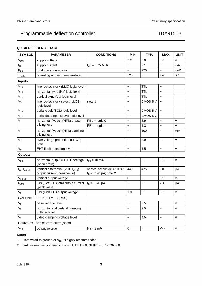
QUICK REFERENCE DATA
Notes
1. Hard wired to ground or VCC is highly recommended.
2. DAC values: vertical amplitude = 31; EHT = 0; SHIFT = 3; SCOR = 0.
SYMBOL PARAMETER CONDITIONS MIN. TYP. MAX. UNIT
VCC supply voltage 7.2 8.0 8.8 V
ICC supply current fclk = 6.75 MHz − 27 − mA
Ptot total power dissipation − 220 − mW
Tamb operating ambient temperature −25 − +70 °C
Inputs
V14 line-locked clock (LLC) logic level − TTL −V13 horizontal sync (HA) logic level − TTL −V12 vertical sync (VA) logic level − TTL −V5 line-locked clock select (LLCS)
logic levelnote 1 − CMOS 5 V −
V18 serial clock (SCL) logic level − CMOS 5 V −V17 serial data input (SDA) logic level − CMOS 5 V −V1 horizontal flyback (HFB) phase
slicing levelFBL = logic 0 − 3.9 − V
FBL = logic 1 − 1.3 − V
V1 horizontal flyback (HFB) blankingslicing level
− 100 − mV
V3 over voltage protection (PROT)level
− 3.9 − V
V9 EHT flash detection level − 1.5 − V
Outputs
V20 horizontal output (HOUT) voltage(open drain)
I20 = 10 mA − − 0.5 V
I11−I10(M) vertical differential (VOUTA, B)output current (peak value)
vertical amplitude = 100%;I8 = −120 µA; note 2
440 475 510 µA
V10,11 vertical output voltage 0 − 3.9 V
I6(M) EW (EWOUT) total output current(peak value)
I8 = −120 µA − − 930 µA
V6 EW (EWOUT) output voltage 1.0 − 5.5 V
SANDCASTLE OUTPUT LEVELS (DSC)
V2 base voltage level − 0.5 − V
V2 horizontal and vertical blankingvoltage level
− 2.5 − V
V2 video clamping voltage level − 4.5 − V
HORIZONTAL OFF-CENTRE SHIFT (OFCS)
V19 output voltage I19 = 2 mA 0 − VCC V
July 1994 4
Philips Semiconductors Preliminary specification
Programmable deflection controller TDA9151B
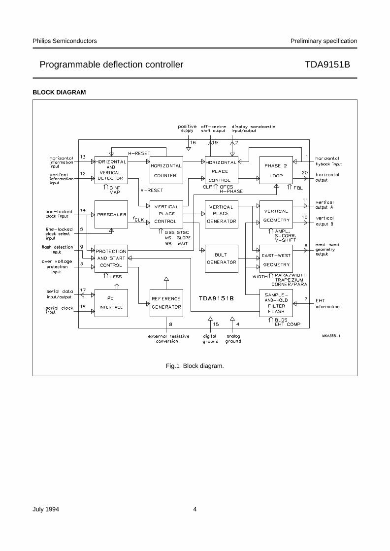
BLOCK DIAGRAM
Fig.1 Block diagram.

July 1994 5
Philips Semiconductors Preliminary specification
Programmable deflection controller TDA9151B
PINNING
SYMBOL PIN DESCRIPTION
HFB 1 horizontal flyback input
DSC 2 display sandcastle input/output
PROT 3 over voltage protection input
AGND 4 analog ground
LLCS 5 line-locked clock selection input
EWOUT 6 east-west geometry output
EHT 7 EHT compensation
RCONV 8 external resistive conversion
FLASH 9 flash detection input
VOUTB 10 vertical output B
VOUTA 11 vertical output A
VA 12 vertical information input
HA 13 horizontal information input
LLC 14 line-locked clock input
DGND 15 digital ground
VCC 16 supply input (+8 V)
SDA 17 serial data input/output
SCL 18 serial clock input
OFCS 19 off-centre shift output
HOUT 20 horizontal outputFig.2 Pin configuration.
FUNCTIONAL DESCRIPTION
Input signals (pins 12, 13, 14, 17 and 18)
The TDA9151B requires three signals for minimumoperation (apart from the supply). These signals are theline-locked clock (LLC) and the two I2C-bus signals (SDAand SCL). Without the LLC the device will not operatebecause the internal synchronous logic uses the LLC asthe system clock.
I2C-bus transmissions are required to enable the device toperform its required tasks. Once started the IC will use theHA and/or VA inputs for synchronization. If the LLC is not
present the outputs will be switched off and all operationsdiscarded (if the LLC is not present the line drive will beinhibited within 2 µs, the EW output current will drop tozero and the vertical output current will drop to 20% of theadjusted value within 100 µs). The SDA and SCL inputsmeet the I2C-bus specification, the other three inputs areTTL compatible.
The LLC frequency can be divided-by-two internally byconnecting LLCS (pin 5) to ground thereby enabling theprescaler.
The LLC timing is given in the Chapter “Characteristics”.

July 1994 6
Philips Semiconductors Preliminary specification
Programmable deflection controller TDA9151B
I2C-bus commands
Slave address: 8C HEX = 1000110X BIN
READ MODE
The format of the status byte is: PON PROT 0 0 0 0 0 0
Where:
PON is the status bit for power-on reset (POR) and afterpower failure:
• Logic 1:
– after the first POR and after power failure; also set to1 after a severe voltage dip that may have disturbedthe various settings
– POR 1 to 0 transition, VCC = 6.25 V (typ.)
– POR 0 to 1 transition, VCC = 5.75 V (typ.)
• Logic 0:
– after a successful read of the status byte.
PROT is the over voltage detection for the scaled EHTinput:
• Logic 1:
– if the scaled EHT rises above the reference value of3.9 V
• Logic 0:
– after a successful read of the status byte and EHT<3.9 V.
Remark : a read action is considered successful when anEnd Of Data signal has been detected (i.e. no masteracknowledge).
Table 1 Write mode with auto increment; subaddress and data byte format.
Notes
1. X = don’t care.
2. Data bit used in another function.
FUNCTION SUBADDRESSDATA BYTE
D7 D6 D5 D4 D3 D2 D1 D0
Vertical amplitude 00 X(1) X A5 A4 A3 A2 A1 A0
Vertical S-correction 01 X X A5 A4 A3 A2 A1 A0
Vertical start scan 02 X X A5 A4 A3 A2 A1 A0
Vertical off-centre shift 03 X note 2 note 2 note 2 X A2 A1 A0
EW trapezium correction 03 X A6 A5 A4 X note 2 note 2 note 2
EW width/width ratio 04 X X A5 A4 A3 A2 A1 A0
EW parabola/width ratio 05 X X A5 A4 A3 A2 A1 A0
EW corner/parabola ratio 06 X X A5 A4 A3 A2 A1 A0
EHT compensation 07 X X A5 A4 A3 A2 A1 A0
Horizontal phase 08 X X A5 A4 A3 A2 A1 A0
Horizontal off-centre shift 09 X X A5 A4 A3 A2 A1 A0
Clamp shift 0A X X X X X A2 A1 A0
Control 1 0B MS WS FBL VAP BLDS LFSS DINT GBS
Vertical slope MSB 0C A7 A6 A5 A4 A3 A2 A1 A0
Vertical slope LSB 0D A7 A6 A5 A4 A3 A2 A1 A0
Vertical wait 0E A7 A6 A5 A4 A3 A2 A1 A0
Control 2 0F X X X VPR CPR DIP PRD CSU
July 1994 7
Philips Semiconductors Preliminary specification
Programmable deflection controller TDA9151B
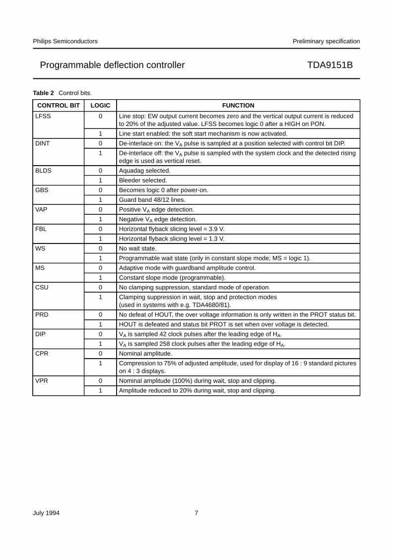
Table 2 Control bits.
CONTROL BIT LOGIC FUNCTION
LFSS 0 Line stop: EW output current becomes zero and the vertical output current is reducedto 20% of the adjusted value. LFSS becomes logic 0 after a HIGH on PON.
1 Line start enabled: the soft start mechanism is now activated.
DINT 0 De-interlace on: the VA pulse is sampled at a position selected with control bit DIP.
1 De-interlace off: the VA pulse is sampled with the system clock and the detected risingedge is used as vertical reset.
BLDS 0 Aquadag selected.
1 Bleeder selected.
GBS 0 Becomes logic 0 after power-on.
1 Guard band 48/12 lines.
VAP 0 Positive VA edge detection.
1 Negative VA edge detection.
FBL 0 Horizontal flyback slicing level = 3.9 V.
1 Horizontal flyback slicing level = 1.3 V.
WS 0 No wait state.
1 Programmable wait state (only in constant slope mode; MS = logic 1).
MS 0 Adaptive mode with guardband amplitude control.
1 Constant slope mode (programmable).
CSU 0 No clamping suppression, standard mode of operation.
1 Clamping suppression in wait, stop and protection modes(used in systems with e.g. TDA4680/81).
PRD 0 No defeat of HOUT, the over voltage information is only written in the PROT status bit.
1 HOUT is defeated and status bit PROT is set when over voltage is detected.
DIP 0 VA is sampled 42 clock pulses after the leading edge of HA.
1 VA is sampled 258 clock pulses after the leading edge of HA.
CPR 0 Nominal amplitude.
1 Compression to 75% of adjusted amplitude, used for display of 16 : 9 standard pictureson 4 : 3 displays.
VPR 0 Nominal amplitude (100%) during wait, stop and clipping.
1 Amplitude reduced to 20% during wait, stop and clipping.
July 1994 8
Philips Semiconductors Preliminary specification
Programmable deflection controller TDA9151B
Table 3 Explanation of control bits shown in Table 2.
Table 4 Clock frequency control bit (pin 5; note 1).
Note
1. Switching of the prescaler is only allowed when LFSS is LOW. It is highly recommended to hard wire LLCS to groundor VCC. Active switching may damage the output power transistor due to the changing HOUT pulse. This may causevery high currents and large flyback pulses. The permitted combinations of LLC and the prescaler are shown inTable 5.
Table 5 Line duration with prescaler.
Note
1. Combination not allowed.
CONTROL BITS DESCRIPTION
LFSS line frame start/stop
DINT de-interlace
BLDS bleeder mode selection
GBS guard band selection
VAP polarity of VA edge detection
FBL flyback slicing level
WS wait state on/off
MS mode select
CSU clamping suppression mode
PRD protection/detection mode
DIP de-interlace phase
CPR compression on/off
VPR vertical power reduction mode
CONTROL BIT LOGIC FUNCTION
LLCS 0 prescaler on: the internal clock frequency fclk = 1⁄2fLLC
1 prescaler off (default by internal pull-up resistor): the internal clock frequency fclk = fLLC
LLC (MHz) ON (µs) OFF (µs)
6.75 note 1 64
13.5 64 32
27 32 note 1
July 1994 9
Philips Semiconductors Preliminary specification
Programmable deflection controller TDA9151B
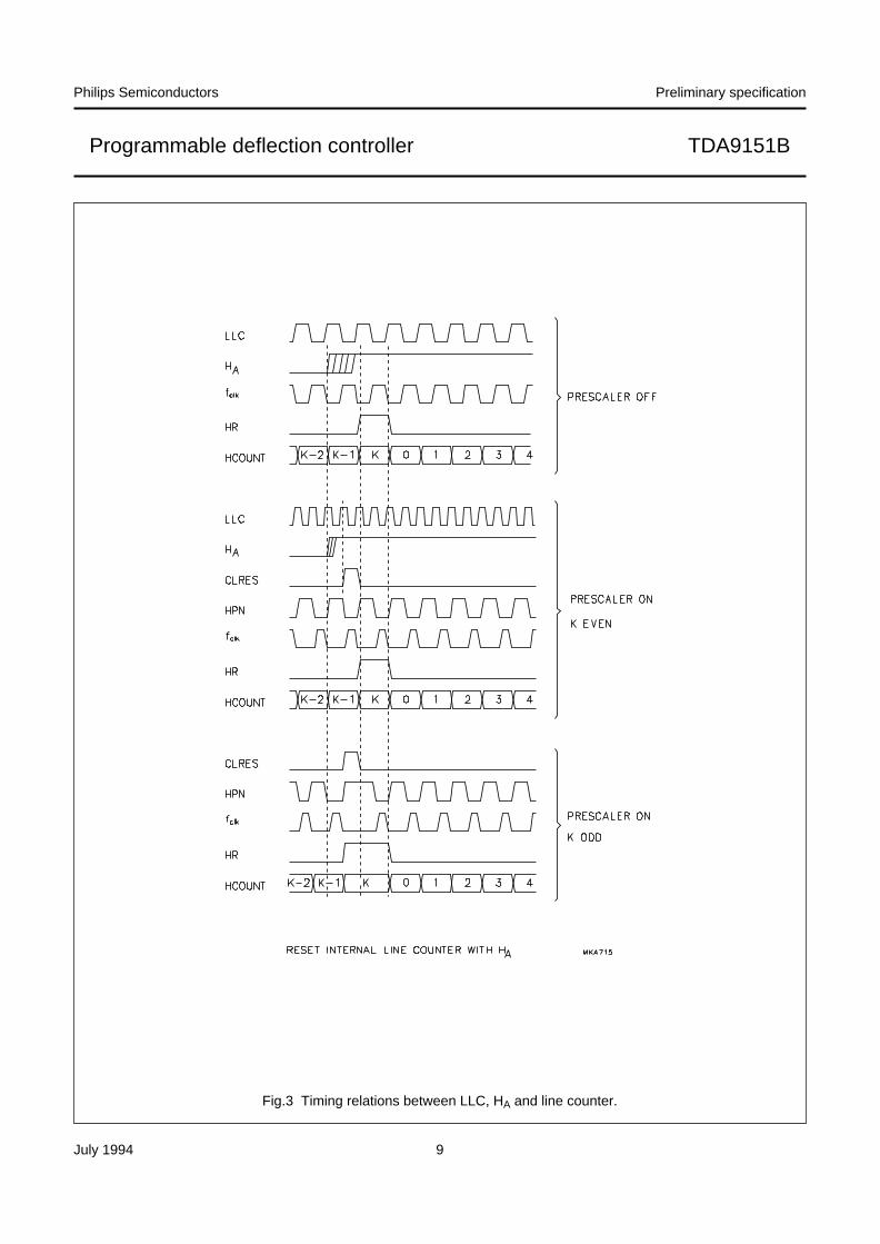
Fig.3 Timing relations between LLC, HA and line counter.
July 1994 10
Philips Semiconductors Preliminary specification
Programmable deflection controller TDA9151B
Horizontal part (pins 1, 2, 13, 19 and 20
SYNCHRONIZATION PULSE
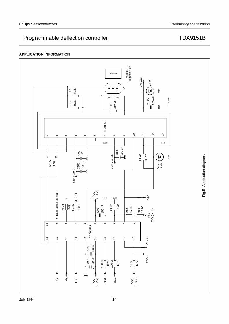
The HA input (pin 13) is a TTL-compatible CMOS input.Pulses on this input have to fulfil the timing requirementsas illustrated in Fig.6. For correct detection the minimumpulse width for both the HIGH and LOW periods is 2internal clock periods.
FLYBACK INPUT PULSE
The HFB input (pin 1) is a CMOS input. The delay of thecentre of the flyback pulse to the leading edge of the HApulse can be set via the I2C-bus with the horizontal phasebyte (subaddress 08), as illustrated in Fig.7.The resolution is 6-bit.
OUTPUT PULSE
The HOUT pulse (pin 20) is an open-drain NMOS output.The duty factor for this output is typically 52⁄48(conducting/non-conducting) during normal operation. Asoft start causes the duty factor to increase linearly from 5to 52% over a minimum period of 2000 lines in 2000 steps.
OFF-CENTRE SHIFT
The OFCS output (pin 19) is a push-pull CMOS outputwhich is driven by a pulse-width modulated DAC.
By using a suitable interface, the output signal can be usedfor off-centre shift correction in the horizontal output stage.This correction is required for HDTV tubes with a 16 × 9aspect ratio and is useful for high performance flat squaretubes to obtain the required horizontal linearity. Forapplications where off-centre correction is not required,the output can be used as an auxiliary DAC. The OFCSsignal is phase-locked with the line frequency. Theoff-centre shift can be set via the I2C-bus, subaddress 09,with a 6-bit resolution as illustrated in Fig.8.
SANDCASTLE
The DSC input/output (pin 2) acts as a sandcastlegenerating output and a guard sensing input. As an outputit provides 2 levels (apart from the base level), one for thehorizontal and vertical blanking and the other for the videoclamping. As an input it acts as a current sensor during thevertical blanking interval for guard detection.
CLAMPING PULSE
The clamping pulse width is 21 internal clock periods. Theshift, with respect to HA can be varied from 35 to 49 clockperiods in 7 steps via the I2C-bus, clamp shift bytesubaddress 0A, as illustrated in Fig.9. It is possible tosuppress the clamping pulse during wait, stop andprotection modes with control bit CSU. This will avoidunwanted reset of the TDA4680/81 (only used in thosecircuits).
HORIZONTAL BLANKING
The start of the horizontal blanking pulse is minimum 38and maximum 41 clock periods before the centre of theflyback pulse, depending on the fclk/fH ratio K inaccordance with 41 − (432 − K).
Stop of the horizontal blanking pulse is determined by thetrailing edge of the HFB pulse at the horizontal blankingslicing level crossing as illustrated in Fig.10.
VERTICAL BLANKING
The vertical blanking pulse starts two internal clock pulsesafter the rising edge of the VA pulse. During this interval asmall guard pulse, generated during flyback by the verticalpower output stage, must be inserted. Stop verticalblanking is effected at the end of the blanking interval onlywhen the guard pulse is present (see Section “Verticalguard”).
The start scan setting determines the end of verticalblanking with a 6-bit resolution in steps of one line via theI2C-bus subaddress 02 (see Figs 11, 12 and 13).
VERTICAL GUARD
In the vertical blanking interval a small unblanking pulse isinserted. This pulse must be filled-in by a blanking pulse orguard pulse from the vertical power output stage whichwas generated during the flyback period. In this conditionthe sandcastle output acts as guard detection input andrequires a minimum 800 µA input current. This current issensed during the unblanking period. Vertical blanking isonly stopped at the end of the blanking interval when theinserted pulse is present. In this way the picture tube isprotected against damage in the event of missing ormalfunctioning vertical deflection (see Figs 11, 12 and 13).
July 1994 11
Philips Semiconductors Preliminary specification
Programmable deflection controller TDA9151B
Vertical part (pins 6, 8, 10, 11 and 12)
SYNCHRONIZATION PULSE
The VA input (pin 12) is a TTL-compatible CMOS input.Pulses at this input have to fulfil the timing requirements asillustrated in Fig.6. For correct detection the minimumpulse width for both the HIGH and LOW period is 2 internalclock periods. For further requirements on minimum pulsewidth see also Section “De-interlace”.
VERTICAL PLACE GENERATOR
An overview of the various modes of operation of thevertical place generator is illustrated in Fig.13.
With control bit CPR a compress to 75% of the adjustedvalues is possible in all modes of operation. This control bitis used to display 16 : 9 standard pictures on 4 : 3displays. No new adjustment of other corrections, such ascorner and S-correction, is required.
With control bit VPR a reduction of the current duringclipping, wait and stop modes to 20% of the nominal valuecan be selected, which will reduce the dissipation in thevertical drive circuits.
Vertical place generator in adaptive mode (MS = logic 0)
The vertical start-scan data (subaddress 02) determinesthe vertical placement in the total range of 64 × 432 clockperiods in 63 steps. The maximum number ofsynchronized lines per scan is 910 with an equivalent fieldfrequency of 17.2 or 34.4 Hz for fH = 15625 or 31250 Hzrespectively.
The minimum number of synchronized lines per scan is200 with an equivalent field frequency of 78 or 156 Hz forfH = 15 625 or 31250 Hz respectively.
If the VA pulse is not present, the number of lines per scanwill increase to 910.2. If the LLC is not present the verticalblanking will start within 2 µs.
Amplitude control is automatic, with a settling time of 1 to2 new fields and an accuracy of either 16/12 or 48/12 linesdepending on the value of the GBS bit.
Differences in the number of lines per field, as can occur inTXT or in multi-head VTR, will not affect the amplitudesetting providing the differences are less than the valueselected with GBS. This is called amplitude controlguardband. The difference sequence and the differencesequence length are not important.
Vertical place generator in constant slope mode(MS = logic 1)
In this mode the slope can be programmed directly with atwo byte value on subaddress 0C (MSB) and 0D (LSB).When the actual number of lines is greater than theprogrammed number of lines, the circuit will enter the stopstate in which the differential vertical output currentremains 100% or drops to 20% (programmable withcontrol bit VPR). The programmed value for the slope isthe required number of lines multiplied by 72. Theprogramming limits are; minimum 200 × 72 and maximum910 × 72.
A vertical expansion is obtained with a combination ofslope data and a programmable wait status, atsubaddress 0E. The wait status is selected with control bitMS and can only be activated in the constant slope mode.The wait state is an 8-bit value, programmable from 0 to255. The actual wait state is one line longer than theprogrammed value. If blanking is applied during stop andwait status the differential output current will be the samewith VPR selected value (20 or 100%).
DE-INTERLACE
With de-interlace on (DINT = logic 0), the VA pulse issampled with LLC at a position supplied by control bit DIP(de-interlace phase).
When DIP = logic 0 sampling takes place 42 clock pulsesafter the leading edge of HA (T = Tline × 42/432).
When DIP = logic 1 sampling takes place 258 clock pulsesafter the leading edge of HA (T = Tline × 258/432).
The distance between the two selectable sampling pointsis (Tline × (258 − 42)/432) which is exactly half a line, thusde-interlace is possible in two directions.
The duration of the VA pulse must, therefore, be sufficientto enable the HA pulse to caught, in this event an activetime of minimum of half a line (see Fig.14 which has anintegration time of Tline × 1⁄4 for the VA pulse).
With de-interlace off, the VA pulse is sampled with thesystem clock. The leading edge is detected and used asthe vertical reset. Selection of the positive or negativeleading edge is achieved by the control bit VAP.

July 1994 12
Philips Semiconductors Preliminary specification
Programmable deflection controller TDA9151B
VERTICAL GEOMETRY PROCESSING
The vertical geometry processing is DC-coupled andtherefore independent of field frequency. The externalresistive conversion (RCONV) at pin 8 sets the referencecurrent for both the vertical and EW geometry processing.A useful range is 100 to 150 µA, the recommended valueis 120 µA.
VERTICAL OUTPUTS
The vertical outputs VOUTA and VOUTB on pins 10 and 11together form a differential current output. The verticalamplitude can be varied over the range 80 to 120% in63 steps via the I2C-bus (subaddress 00). VerticalS-correction is also applied to these outputs and can beset from 0 to 16% by subaddress 01 with a 6-bit resolution.
The vertical off-centre shift (OFCS) shifts the verticaldeflection current zero crossing with respect to the EWparabola bottom. The control range is −1.5 to +1.5%(±1⁄8 × I8) in 7 steps set by the least significant nibble atsubaddress 03.
EW GEOMETRY PROCESSING
The EW geometry processing is DC coupled and thereforeindependent of field frequency. RCONV sets the referencecurrent for both the vertical and EW geometry processing.
The EW output is an ESD-protected single-ended currentoutput.
The EW width/width ratio can be set from 100 to 80% in63 steps via subaddress 04 and the EW parabola/widthratio from 0 to 20% via subaddress 05. The EWcorner/EW parabola ratio has a control range of −40 to 0%in 63 steps via subaddress 06.
The EW trapezium correction can be set from−1.5 to +1.5% in 7 steps via the most significant nibble atsubaddress 03.
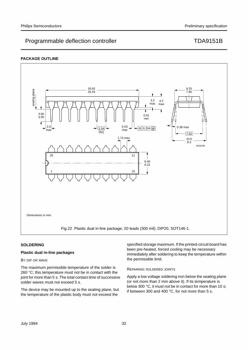
BULT GENERATOR
The Bult generator makes the EW waveform continuous(see Fig.21).
Protection input (pin 3)
The protection input (PROT) is a CMOS input.
The input voltage must be EHT scaled and has thefollowing characteristics:
Two modes of protection are available with the aid ofcontrol bit PRD.
• With PRD = logic 1 the protection mode is selected,HOUT will be defeated and the PROT bit in the statusword is set if the input voltage is above 3.9 V. Thus thedeflection stops and EW output current is zero, while thevertical output current is reduced to 20% of the adjustedvalue. A new start of the circuit is I2C-bus controlled withthe user software.
• With PRD = logic 0 the detection mode is selected,HOUT will not be defeated and the over voltageinformation is only written in the PROT status bit and canbe read by the I2C-bus.
All further actions, such as a write of the LFSS bit, areachieved by the I2C-bus. They depend on theconfiguration used and are defined by user software.
Flash detection/protection input (pin 9)
The FLASH input is a CMOS input with an internal pull-upcurrent of approximately 8 µA.
When a negative-going edge crosses the 0.75 V level arestart will be executed with a soft start of approximately2000 lines, such as in the soft-start mode. When thefunction is not used pin 9 can be connected to ground, VCCor left open-circuit, the internal pull-up current source willprevent any problems. However a hard wired connectionto VCC or ground is recommended when the function is notused.
EHT compensation (pin 7)
The EHT input is a CMOS input.
The EHT compensation input permits scan amplitudemodulation should the EHT supply not be perfect. Forcorrect tracking of the vertical and horizontal deflection thegain of the EW output stage, provided by the ratioRCONV-EW/RCONV, must be 1⁄16Vscan × Vref (see Fig.15).
The input for EHT compensation can be derived from anEHT bleeder or from the picture tubes aquadag(subaddress 0B, bit BLDS).
EHT compensation can be set via subaddress 07 in63 steps allowing a scan modulation range from−10 to +9.7%.
July 1994 13
Philips Semiconductors Preliminary specification
Programmable deflection controller TDA9151B
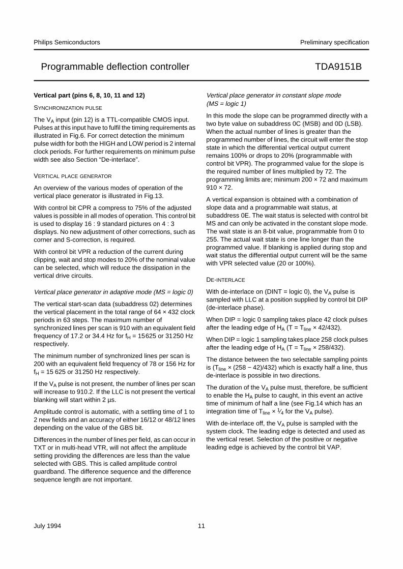
INTERNAL CIRCUITRY
handbook, full pagewidth
300
Ω
12
300
Ω
34
300
Ω
56
MB
D90
6
300
Ω
78
300
Ω
910
300
Ω
1415
16
300
Ω
17
300
Ω
1819
20
300
Ω
13
300
Ω
1211
TD
A91
51B
Fig
.4 I
nter
nal c
ircui
try.
July 1994 14
Philips Semiconductors Preliminary specification
Programmable deflection controller TDA9151B
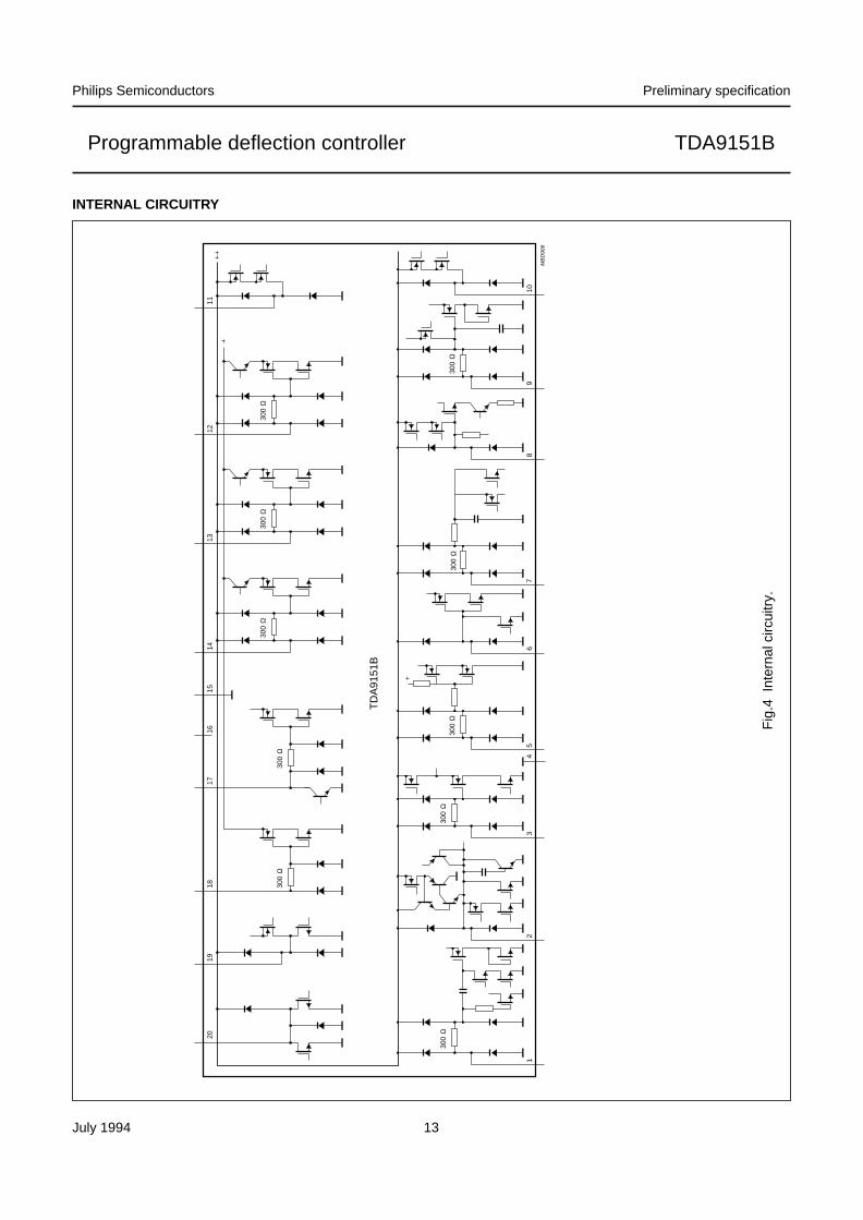
APPLICATION INFORMATION
Fig
.5 A
pplic
atio
n di
agra
m.
handbook, full pagewidth
MB
D90
7
C95
C89
22 µ
F10
0 nF
VC
C(
8 V
)
SD
A10
0 Ω
R75
SC
L10
0 Ω
R76
1 kΩ
R77
TD
A91
51B
VC
C(
8 V
)
HO
UT
OF
CS20191817161514131211
10 9 8 7 6 5 4 3 2 1
LLCHVA A
R99
3.3
kΩ
C97
100
nF
VC
C(
8 V
)
4.7
kΩ
39 k
Ω
EH
T
R87
R88
3.3
kΩ
R84
15 k
Ω
R85
HF
B23
V (
peak
)D
SC
1 2 3 4 5 6 7 8 9 10 11 12 13
R11
3R
117
1 2 333
0 Ω
R
113
C10
5
100
µF10
0nF C
105
100
µF
TD
A83
50
R10
7
82 k
Ω
C11
0
100
nF33
V
EW
-OU
Tvert
ical
defle
ctio
n co
il
LV
3 kΩ
R
105
IE5
IE5
flash
det
ectio
n in
put
Zen
erdi
ode
16 V
(ve
rt)
45 V
(ve
rt)
July 1994 15
Philips Semiconductors Preliminary specification
Programmable deflection controller TDA9151B
TIMING DIAGRAMS
Fig.6 Timing requirements for LLC, HA and VA.
NNNNNNNNNNNNNN
Fig.7 Horizontal phase and HOUT control range.
July 1994 16
Philips Semiconductors Preliminary specification
Programmable deflection controller TDA9151B
Fig.8 OFCS duty factor.
Fig.9 DSC clamping pulse.
July 1994 17
Philips Semiconductors Preliminary specification
Programmable deflection controller TDA9151B
Fig.10 DSC line blanking.
Fig.11 DCS vertical blanking with unblanking.
July 1994 18
Philips Semiconductors Preliminary specification
Programmable deflection controller TDA9151B
Fig.12 DSC with guard interval; start scan = 24.
Vertical blanking LOW period: during scan, during unblanking.
Vertical blanking HIGH period (2.5 V): during STSC, stop and wait.
Vertical blanking continuously HIGH: POR = logic 1, LFSS = logic 0, no guard detected.

July 1994 19
Philips Semiconductors Preliminary specification
Programmable deflection controller TDA9151B
Fig
.13
Ver
tical
def
lect
ion
oper
atin
g m
odes
.
t ub
= u
nbla
nkin
g pu
lse
wid
th.
July 1994 20
Philips Semiconductors Preliminary specification
Programmable deflection controller TDA9151B
I = start VA for DINT = logic 1.
D = start VA for DINT = logic 0.
Fig.14 De-interlace timing.
Fig.15 Explanation of RCONV-EW/RCONV ratio.
July 1994 21
Philips Semiconductors Preliminary specification
Programmable deflection controller TDA9151B
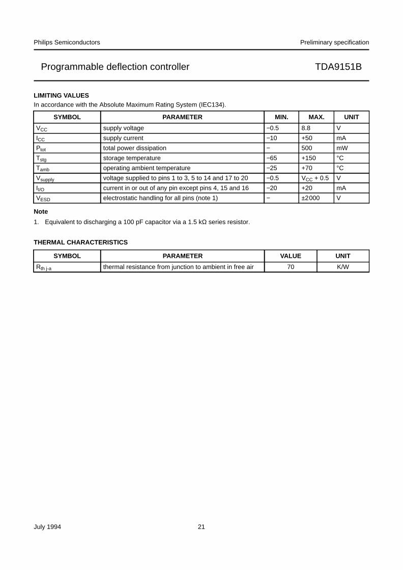
LIMITING VALUESIn accordance with the Absolute Maximum Rating System (IEC134).
Note
1. Equivalent to discharging a 100 pF capacitor via a 1.5 kΩ series resistor.
THERMAL CHARACTERISTICS
SYMBOL PARAMETER MIN. MAX. UNIT
VCC supply voltage −0.5 8.8 V
ICC supply current −10 +50 mA
Ptot total power dissipation − 500 mW
Tstg storage temperature −65 +150 °CTamb operating ambient temperature −25 +70 °CVsupply voltage supplied to pins 1 to 3, 5 to 14 and 17 to 20 −0.5 VCC + 0.5 V
II/O current in or out of any pin except pins 4, 15 and 16 −20 +20 mA
VESD electrostatic handling for all pins (note 1) − ±2000 V
SYMBOL PARAMETER VALUE UNIT
Rth j-a thermal resistance from junction to ambient in free air 70 K/W

July 1994 22
Philips Semiconductors Preliminary specification
Programmable deflection controller TDA9151B
CHARACTERISTICSVCC = 8 V; Tamb = 25 °C; DGND = AGND = 0 V; unless otherwise specified.
SYMBOL PARAMETER CONDITIONS MIN. TYP. MAX. UNIT
Supply
VCC supply voltage 7.2 8.0 8.8 V
ICC supply current note 1;fclk = 6.75 MHz
− 27 − mA
Ptot total power dissipation − 220 − mW
Vpor power-on reset POR 1-to-0transition
− 6.25 7.0 V
POR 0-to-1transition
5.0 5.75 − V
SDA and SCL (pins 17 and 18)
V17 SDA input voltage 0 − 5.5 V
VIL LOW level input voltage (pin 17) − − 1.5 V
VIH HIGH level input voltage (pin 17) 3.5 − − V
IIL LOW level input current (pin 17) V17 = VSSD − − −10 µA
IIH HIGH level input current (pin 17) V17 = VCC − − 10 µA
VOL LOW level output voltage (pin 17) IIL = 3 mA − − 0.4 V
V18 SCL input voltage 0 − 5.5 V
VIL LOW level input voltage (pin 18) − − 1.5 V
VIH HIGH level input voltage (pin 18) 3.5 − − V
IIL LOW level input current (pin 18) V18 = VSSD − − −10 µA
IIH HIGH level input current (pin 18) V18 = VCC − − 10 µA
Line-locked clock and line-locked clock select (pins 14 and 5)
VIL LOW level input voltage (pin 14) − − 0.8 V
VIH HIGH level input voltage (pin 14) 2.0 − − V
I14 input current V14 = <5.5 V −10 − +10 µA
tr rise time 0 − 1⁄2tLLC
tf fall time 0 − 1⁄2tLLC
δ0 duty factor LLCS = logic 0;at 1.4 V; note 2
40 50 60 %
δ1 duty factor LLCS = logic 1;at 1.4 V; note 2
25 50 75 %
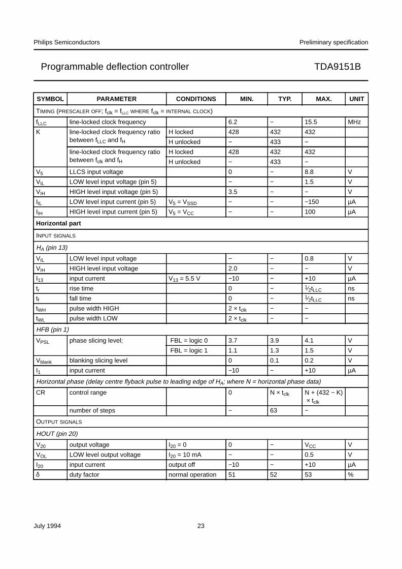
TIMING (PRESCALER ON; fclk = 1⁄2fLLC WHERE fclk = INTERNAL CLOCK)
fLLC line-locked clock frequency 12.4 − 29.2 MHz
K line-locked clock frequency ratiobetween fLLC and fH
H locked 856 864 865
H unlocked − 866 −line-locked clock frequency ratiobetween fclk and fH
H locked 428 432 432.5
H unlocked − 433 −
July 1994 23
Philips Semiconductors Preliminary specification
Programmable deflection controller TDA9151B
TIMING (PRESCALER OFF; fclk = fLLC WHERE fclk = INTERNAL CLOCK)
fLLC line-locked clock frequency 6.2 − 15.5 MHz
K line-locked clock frequency ratiobetween fLLC and fH
H locked 428 432 432
H unlocked − 433 −line-locked clock frequency ratiobetween fclk and fH
H locked 428 432 432
H unlocked − 433 −V5 LLCS input voltage 0 − 8.8 V
VIL LOW level input voltage (pin 5) − − 1.5 V
VIH HIGH level input voltage (pin 5) 3.5 − − V
IIL LOW level input current (pin 5) V5 = VSSD − − −150 µA
IIH HIGH level input current (pin 5) V5 = VCC − − 100 µA
Horizontal part
INPUT SIGNALS
HA (pin 13)
VIL LOW level input voltage − − 0.8 V
VIH HIGH level input voltage 2.0 − − V
I13 input current V13 = 5.5 V −10 − +10 µA
tr rise time 0 − 1⁄2tLLC ns
tf fall time 0 − 1⁄2tLLC ns
tWH pulse width HIGH 2 × tclk − −tWL pulse width LOW 2 × tclk − −
HFB (pin 1)
VPSL phase slicing level; FBL = logic 0 3.7 3.9 4.1 V
FBL = logic 1 1.1 1.3 1.5 V
Vblank blanking slicing level 0 0.1 0.2 V
I1 input current −10 − +10 µA
Horizontal phase (delay centre flyback pulse to leading edge of HA; where N = horizontal phase data)
CR control range 0 N × tclk N + (432 − K)× tclk
number of steps − 63 −
OUTPUT SIGNALS
HOUT (pin 20)
V20 output voltage I20 = 0 0 − VCC V
VOL LOW level output voltage I20 = 10 mA − − 0.5 V
I20 input current output off −10 − +10 µA
δ duty factor normal operation 51 52 53 %
SYMBOL PARAMETER CONDITIONS MIN. TYP. MAX. UNIT

July 1994 24
Philips Semiconductors Preliminary specification
Programmable deflection controller TDA9151B
Soft start (duty factor controlled line drive)
tW initial pulse width soft start − − 5 %
CR control range 5 − 53 %
tss soft start time 1500 − 3000 lines
Switch-off time to the centre of the flyback pulse
CR control range note 3 0 − 160 −(432 − K)× tclk
Φ control sensitivity (loop gain) 400 1000 − µs/µs
k correction factor note 4 − 0.5 −σ sigma value of phase jitter note 5 − 750 − ps
PSRR power supply rejection ratio − − 10 ns/V
Horizontal off-centre shift (pin 19; N = off-centre shift data)
V19 output voltage 0 − VCC V
VOL LOW level output voltage I19 = 2 mA − − 0.5 V
VOH HIGH level output voltage I19 = −2 mA VCC − 0.5 − − V
δ(max) maximum duty factor N <54 1/K (8N+1)/K 425/K %
δ duty factor N ≥54 − 1 − %
number of steps − 54 −
SANDCASTLE (PIN 2)
DSC output voltage
Vclamp video clamping voltage 4.0 4.5 5.0 V
Vblank horizontal and vertical blankingvoltage level
2.0 2.5 3.0 V
Vbase base voltage level 0 0.5 1.0 V
I2 output current guard not detected −1.0 − +0.35 mA
guard detected 0.8 − 2.5 mA
tr rise time − 60 − ns
tf fall time − 60 − ns
Clamping pulse (N = clamp pulse shift data)
tW clamping pulse width − 21 × tclk −tclamp clamp pulse shift w.r.t HA 35 (2N + 35)
× tclk
49
number of steps − 7 −tstart start of horizontal blanking before
middle of flyback pulse38 41 −
(432 − K)× tclk
41
SYMBOL PARAMETER CONDITIONS MIN. TYP. MAX. UNIT
July 1994 25
Philips Semiconductors Preliminary specification
Programmable deflection controller TDA9151B
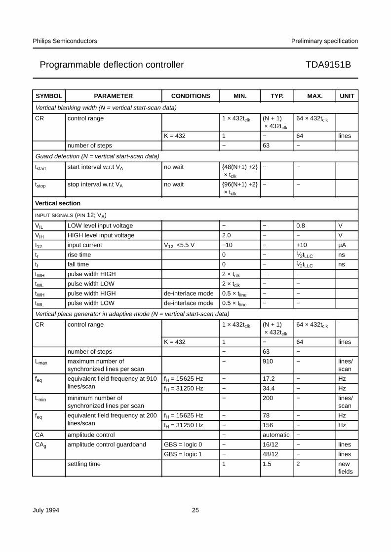
Vertical blanking width (N = vertical start-scan data)
CR control range 1 × 432tclk (N + 1)× 432tclk
64 × 432tclk
K = 432 1 − 64 lines
number of steps − 63 −
Guard detection (N = vertical start-scan data)
tstart start interval w.r.t VA no wait 48(N+1) +2× tclk
− −
tstop stop interval w.r.t VA no wait 96(N+1) +2× tclk
− −
Vertical section
INPUT SIGNALS (PIN 12; VA)
VIL LOW level input voltage − − 0.8 V
VIH HIGH level input voltage 2.0 − − V
I12 input current V12 <5.5 V −10 − +10 µA
tr rise time 0 − 1⁄2tLLC ns
tf fall time 0 − 1⁄2tLLC ns
tWH pulse width HIGH 2 × tclk − −tWL pulse width LOW 2 × tclk − −tWH pulse width HIGH de-interlace mode 0.5 × tline − −tWL pulse width LOW de-interlace mode 0.5 × tline − −
Vertical place generator in adaptive mode (N = vertical start-scan data)
CR control range 1 × 432tclk (N + 1)× 432tclk
64 × 432tclk
K = 432 1 − 64 lines
number of steps − 63 −Lmax maximum number of
synchronized lines per scan− 910 − lines/
scan
feq equivalent field frequency at 910lines/scan
fH = 15625 Hz − 17.2 − Hz
fH = 31250 Hz − 34.4 − Hz
Lmin minimum number ofsynchronized lines per scan
− 200 − lines/scan
feq equivalent field frequency at 200lines/scan
fH = 15625 Hz − 78 − Hz
fH = 31250 Hz − 156 − Hz
CA amplitude control − automatic −CAg amplitude control guardband GBS = logic 0 − 16/12 − lines
GBS = logic 1 − 48/12 − lines
settling time 1 1.5 2 newfields
SYMBOL PARAMETER CONDITIONS MIN. TYP. MAX. UNIT
July 1994 26
Philips Semiconductors Preliminary specification
Programmable deflection controller TDA9151B
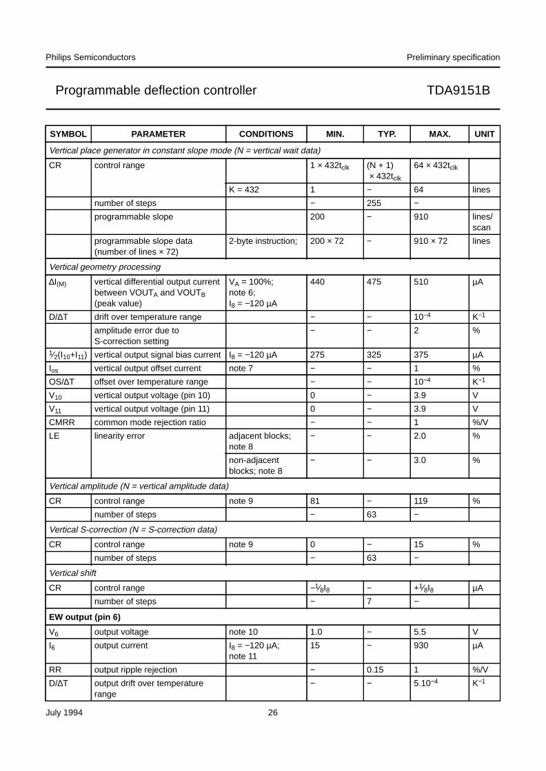
Vertical place generator in constant slope mode (N = vertical wait data)
CR control range 1 × 432tclk (N + 1)× 432tclk
64 × 432tclk
K = 432 1 − 64 lines
number of steps − 255 −programmable slope 200 − 910 lines/
scan
programmable slope data(number of lines × 72)
2-byte instruction; 200 × 72 − 910 × 72 lines
Vertical geometry processing
∆I(M) vertical differential output currentbetween VOUTA and VOUTB(peak value)
VA = 100%;note 6;I8 = −120 µA
440 475 510 µA
D/∆T drift over temperature range − − 10−4 K−1
amplitude error due toS-correction setting
− − 2 %
1⁄2(I10+I11) vertical output signal bias current I8 = −120 µA 275 325 375 µA
Ios vertical output offset current note 7 − − 1 %
OS/∆T offset over temperature range − − 10−4 K−1
V10 vertical output voltage (pin 10) 0 − 3.9 V
V11 vertical output voltage (pin 11) 0 − 3.9 V
CMRR common mode rejection ratio − − 1 %/V
LE linearity error adjacent blocks;note 8
− − 2.0 %
non-adjacentblocks; note 8
− − 3.0 %
Vertical amplitude (N = vertical amplitude data)
CR control range note 9 81 − 119 %
number of steps − 63 −
Vertical S-correction (N = S-correction data)
CR control range note 9 0 − 15 %
number of steps − 63 −
Vertical shift
CR control range −1⁄8I8 − +1⁄8I8 µA
number of steps − 7 −
EW output (pin 6)
V6 output voltage note 10 1.0 − 5.5 V
I6 output current I8 = −120 µA;note 11
15 − 930 µA
RR output ripple rejection − 0.15 1 %/V
D/∆T output drift over temperaturerange
− − 5.10−4 K−1
SYMBOL PARAMETER CONDITIONS MIN. TYP. MAX. UNIT
July 1994 27
Philips Semiconductors Preliminary specification
Programmable deflection controller TDA9151B
EW WIDTH/WIDTH RATIO
CR control range note 9 100 − 81 %
Ieq(typ) typical equivalent output current V6 = 3 V 15 − 440 µA
number of steps − 63 −
EW PARABOLA/WIDTH RATIO
CR control range note 9 1 − 19 %
Ieq(typ) typical equivalent output current width = 100% 10 − 430 µA
width = 80% 10 − 345 µA
number of steps − 63 −
EW CORNER/EW PARABOLA RATIO
CR control range notes 9 and 12 40 − 0 %
Ieq(typ) typical equivalent output current width = 100% 0 − 200 µA
width = 80% 0 − 160 µA
number of steps − 63 −
EW TRAPEZIUM CORRECTION
EW trapezium/width ratio note 9 −1.5 − +1.5 %
number of steps − 7 −
EHT input (pin 7)
Vref reference voltage BLDS = logic 1 − 3.9 − V
BLDS = logic 0 − VCC − V
VI input voltage w.r.t Vref BLDS = logic 1 −20 0 +20 %
VI input voltage w.r.t VCC BLDS = logic 0 0 − −2Vref V
mscan scan modulation −10 0 +9.7 %
mGC modulation gain control 0 − 1
number of steps − 63 −II input current −100 − +100 nA
RCONV input (pin 8)
VO output voltage I8 = −120 µA 3.7 3.9 4.1 V
I8 current range −100 −120 −150 µA
PROT input (pin 3)
VI input voltage 0 − VCC V
V3 voltage detection level 3.7 3.9 4.1 V
II input current −10 − +10 µA
FLASH detection input (pin 9)
VI input voltage 0 − VCC V
V9 voltage detection level falling edge 0.5 0.75 1.0 V
H detection level hysteresis 0.3 0.5 0.8 V
I9 detection pull-up current −4 −8 −16 µA
SYMBOL PARAMETER CONDITIONS MIN. TYP. MAX. UNIT
July 1994 28
Philips Semiconductors Preliminary specification
Programmable deflection controller TDA9151B
Notes to the characteristics
1. For all other frequencies the expected supply current will be as shown in Table 6 (fclk is the internal clock frequency,fLLC is the internal clock frequency applied to pin 14).
2. When the prescaler is on, one in two LLC HIGH periods is omitted.
3. For 16 kHz operation the minimum value of the control range is 5.7 µs. With 1⁄2tFB = 5.7 µs the minimum storage timeis 0 and the maximum is 18 µs.
For 32 kHz operation the minimum value of the control range is 0 µs. With 1⁄2tFB = 2.85 µs the minimum storage timeis 0 and the maximum is 9 µs.
4. The k factor is defined as the amount of correction of a phase step. Thus with k = 0.5 a 50% correction of the errortakes place each line. The resulting step response now becomes kn, with n the line number after the step.
5. The sigma value (σ) of the jitter with respect to LLC (HA) at fH = 32 kHz and a storage time of 5 µs.
Measurement of σ is carried out during 200 lines in the active scan, the resulting peak-to-peak value is approximately6σ. The visible jitter on the screen will be higher than the peak-to-peak jitter, depending on the deflection stage.
6. DAC values: vertical amplitude = 31; EHT = 0; SHIFT = 3; SCOR = 0.
7. Value is a percentage of I10 − I11.
8. The linearity error is measured without S-correction and based on the same measurement principle as used for thescreen. Measuring method: divide the output signal I10 − I11 into 22 equal parts, ranging from 1 to 22 inclusive.Measure the value of two succeeding parts called one block starting with part 2 and 3 (block 1) and ending with part20 and 21 (block 10). Thus part 1 and 22 are unused.
Linearity error for adjacent blocks =
Linearity error for non-adjacent blocks =
Where a = amplitude, ak = amplitude block k and aavg = average amplitude.
9. Minimum available range.
10. Selection of test mode.
When the EW output is pulled above VCC − 0.5 V a special test mode is entered in which the prescaler and the clockdetector are disabled.
11. DAC values: vertical amplitude = 31; EHT = 0.
12. The value of −40% (typically 46%) corresponds with data 3F (hexadecimal) and implies maximum 4th ordercompensation.
Table 6 Supply current with prescaler on/off.
Note
1. Combination not allowed.
LLC (MHz) ON (mA) OFF (mA)
6.75 note 1 27
13.5 27 38
27 42 note 1
ak a k 1+( )–
aavg------------------------------
amax amin–
aavg------------------------------
July 1994 29
Philips Semiconductors Preliminary specification
Programmable deflection controller TDA9151B
TEST AND APPLICATION INFORMATION
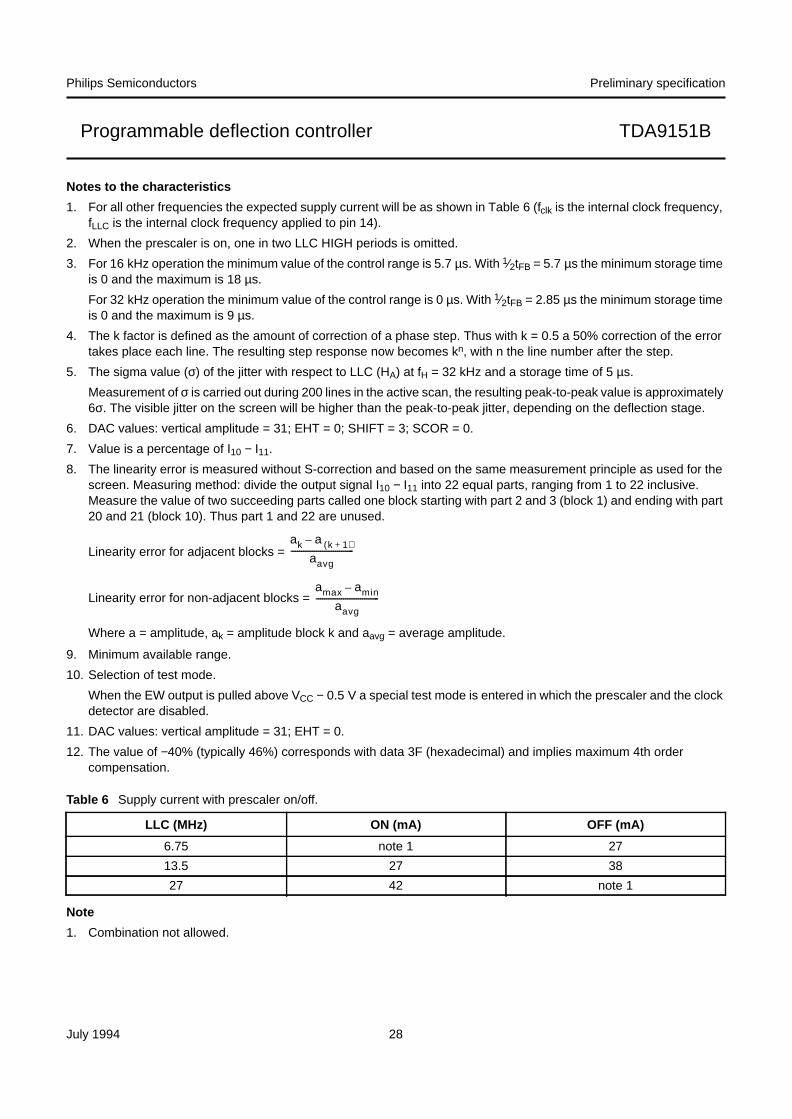
Fig.16 Control range amplitude.
I11 − I10.
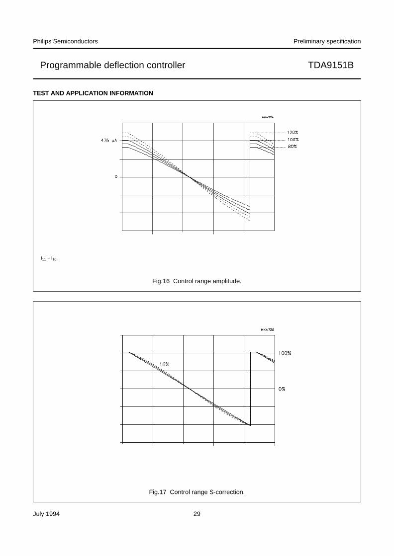
Fig.17 Control range S-correction.
BBBBBBBBBBBBBBBBBBBBBBBBBBBBBBBBBBBBBBBBBBBBBBBBBBBBBBBBBBBBBBBBBBBBBBBBBBBBBBBBBBBBBBBBBBBBBBBBBBBBBBBBBBBBBBBBBBBBBBBBBBBBBBBBBBBBBBBBBBBBBBBBBBBBBBBBBBBBBBBBBBBBBBBBBBBBBBBBBBBBBBBBBBBBBBBBBBBBBBBBBBBBBBBBBBBBBBBBBBBBBBBBBBBBBBBBBBBBBBBBBBBBBBBBBBBBBBBBBBBBBBBBBBBBBBBBBBBBBBBBBBBBBBBBBBBBBBBBBBBBBBBBBBBBBBBBBBBBBBBBBBBBBBBBBBBBBBBBBBBBBBBBBBBBBBBB
July 1994 30
Philips Semiconductors Preliminary specification
Programmable deflection controller TDA9151B
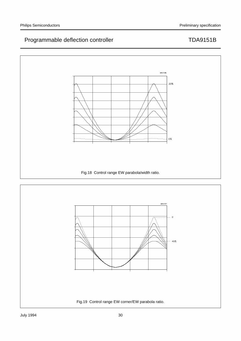
Fig.18 Control range EW parabola/width ratio.
BBBBBBBBBBBBBBBBBBBBBBBBBBBBBBBBBBBBBBBBBBBBBBBBBBBBBBBBBBBBBBBBBBBBBBBBBBBBBBBBBBBBBBBBBBBBBBBBBBBBBBBBBBBBBBBBBBBBBBBBBBBBBBBBBBBBBBBBBBBBBBBBBBBBBBBBBBBBBBBBBBBBBBBBBBBBBBBBBBBBBBBBBBBBBBBBBBBBBBBBBBBBBBBBBBBBBBBBBBBBBBBBBBBBBBBBBBBBBBBBBBBBBBBBBBBBBBBBBBBBBBBBBBBBBBBBBBBBBBBBBBBBBBBBBBBBBBBBBBBBBBBBBBBBBBBBBBBBBBBBBBBBBBBBBBBBBBBBBBBBBBBBB
BBBBBBBBBBBBBBBBBBBBBBBBBBBBBBBBBBBBBBBBBBBBBBBBBBBBBBBBBBBBBBBBBBBBBBBBBBBBBBBBBBBBBBBBBBBBBBBBBBBBBBBBBBBBBBBBBBBBBBBBBBBBBBBBBBBBBBBBBBBBBBBBBBBBBBBBBBBBBBBBBBBBBBBBBBBBBBBBBBBBBBBBBBBBBBBBBBBBBBBBBBBBBBBBBBBBBBBBBBBBBBBBBBBBBBBBBBBBBBBBBBBBBBBBBBBBBBBBBBBBBBBBBBBBBBBBBBBBBBBBBBBBBBBBBBBBBBBBBBBBBBBBBBBBBBBBBBBBBBBBBBBBBBBBBBBBBBBBBBBBBBBBBBBBBBBBBBBBBBBBBBBBBBBBBBBBBBBBBBBBBBBBBBBBBBBBBBBBBBBBBBBBBBBBBBBBBBBBBBBBBBBBB
Fig.19 Control range EW corner/EW parabola ratio.
July 1994 31
Philips Semiconductors Preliminary specification
Programmable deflection controller TDA9151B
BBBBBBBBBBBBBBBBBBBBBBBBBBBBBBBBBBBBBBBBBBBBBBBBBBBBBBBBBBBBBBBBBBBBBBBBBBBBBBBBBBBBBBBBBBBBBBBBBBBBBBBBBBBBBBBBBBBBBBBBBBBBBBBBBBBBBBBBBBBBBBBBBBBBBBBBBBBBBBBBBBBBBBBBBBBBBBBBBBBBBBBBBBBBBBBBBBBBBBBBBBBBBBBBBBBBBBBBBBBBBBBBBBBBBBBBBBBBBBBBBBBBBBBBBBBBBBBBBBBBBBBBBBBBBBBBBBBBBBBBBBBBBBBBBBBBBBBBBBBBBBBBBBBBBBBBBBBBBBBBBBBBBBBBBBBBBBBBBBBBBBBBBBBBBBBBBBBBBBBBBBBBBBBBBBBBBBBBBBBBBBBBBBBBBBBBBBBBBBBB
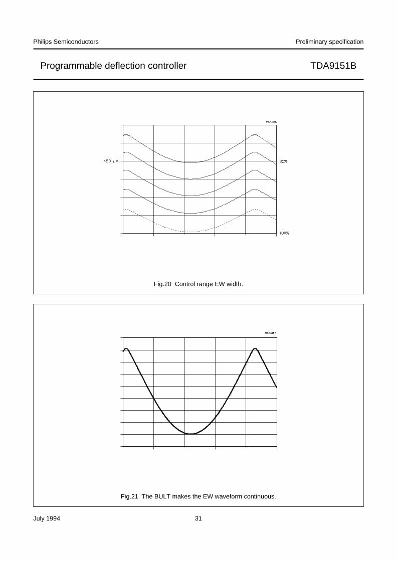
Fig.20 Control range EW width.
Fig.21 The BULT makes the EW waveform continuous.
BBBBBBBBBBBBBBBBBBBBBBBBBBBBBBBBBBBBBBBBBBBBBBBBBBBBBBBBBBBBBBBBBBBBBBBBBBBBBBBBBBBBBBBBBBBBBBBBBBBBBBBBBBBBBBBBBBBBBBBBBBBBBBBBBBBBBBBBBBBBBBBBBBBBBBBBBBBBBBBBBBBBBBBBBBBBBBBBBBBBBBBBBBBBBBBBBBBBBBBBBBBBBBBBBBBBBBBBBBBBBBBBBBBBBBBBBBBBBBBBBBBBBBBBBBBBBBBBBBBBBBBBBBBBBBBBBBBBBBBBBBBBBBBBBBBBBBBBBBBBBBBBBBBBBBBBBBBBBBBBBBBBBBBBBBBBBBBBBBBBBBBBBBBBBBBBBBBBBBBBBBBBBBBBBBBBBBBBBBBBBBBBBBBBBBB
July 1994 32
Philips Semiconductors Preliminary specification
Programmable deflection controller TDA9151B
PACKAGE OUTLINE
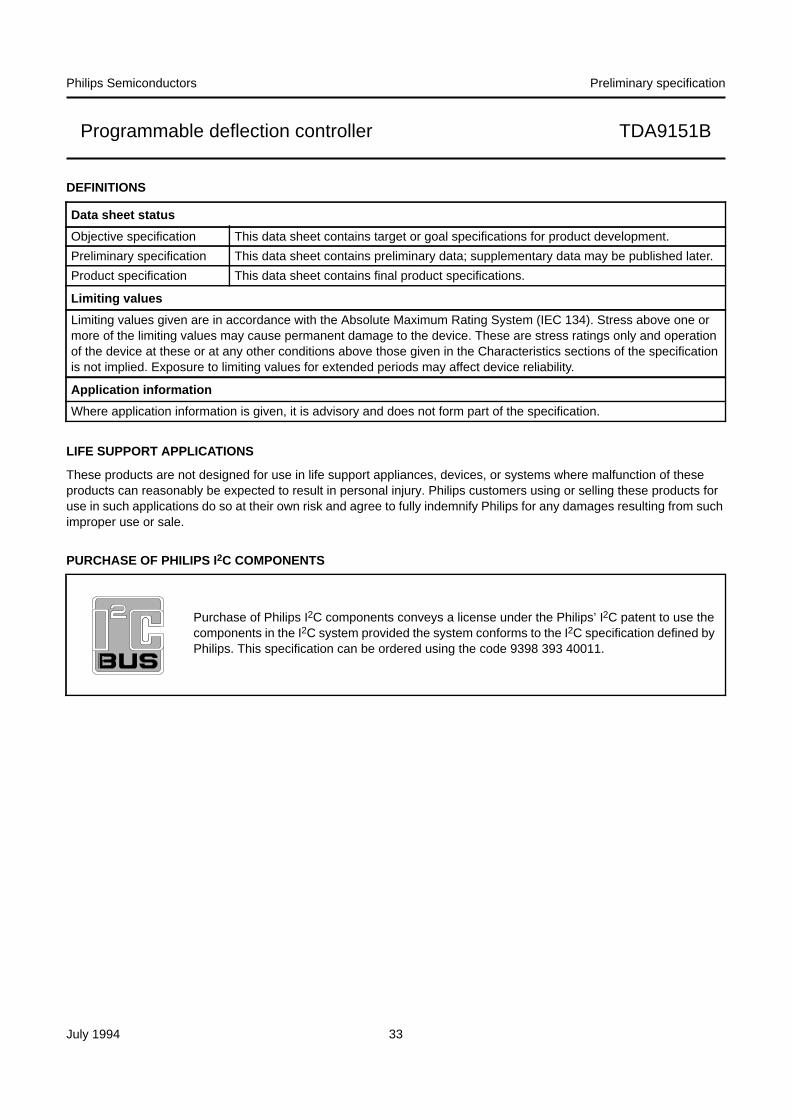
Fig.22 Plastic dual in-line package; 20 leads (300 mil); DIP20, SOT146-1.
Dimensions in mm.
MSA258
2.54(9x)
0.254 M0.53 max
seat
ing
plan
e
3.60 3.05
2.0 max
26.92 26.54
4.2 max
3.2 max
0.51 min
8.25 7.80
0.38 max
7.62
10.0 8.3
11
10
6.40 6.22
1.73 max
20
1
SOLDERING
Plastic dual in-line packages
BY DIP OR WAVE
The maximum permissible temperature of the solder is260 °C; this temperature must not be in contact with thejoint for more than 5 s. The total contact time of successivesolder waves must not exceed 5 s.
The device may be mounted up to the seating plane, butthe temperature of the plastic body must not exceed the
specified storage maximum. If the printed-circuit board hasbeen pre-heated, forced cooling may be necessaryimmediately after soldering to keep the temperature withinthe permissible limit.
REPAIRING SOLDERED JOINTS
Apply a low voltage soldering iron below the seating plane(or not more than 2 mm above it). If its temperature isbelow 300 °C, it must not be in contact for more than 10 s;if between 300 and 400 °C, for not more than 5 s.
July 1994 33
Philips Semiconductors Preliminary specification
Programmable deflection controller TDA9151B
DEFINITIONS
LIFE SUPPORT APPLICATIONS
These products are not designed for use in life support appliances, devices, or systems where malfunction of theseproducts can reasonably be expected to result in personal injury. Philips customers using or selling these products foruse in such applications do so at their own risk and agree to fully indemnify Philips for any damages resulting from suchimproper use or sale.
Data sheet status
Objective specification This data sheet contains target or goal specifications for product development.
Preliminary specification This data sheet contains preliminary data; supplementary data may be published later.
Product specification This data sheet contains final product specifications.
Limiting values
Limiting values given are in accordance with the Absolute Maximum Rating System (IEC 134). Stress above one ormore of the limiting values may cause permanent damage to the device. These are stress ratings only and operationof the device at these or at any other conditions above those given in the Characteristics sections of the specificationis not implied. Exposure to limiting values for extended periods may affect device reliability.
Application information
Where application information is given, it is advisory and does not form part of the specification.
PURCHASE OF PHILIPS I2C COMPONENTS
Purchase of Philips I2C components conveys a license under the Philips’ I2C patent to use thecomponents in the I2C system provided the system conforms to the I2C specification defined byPhilips. This specification can be ordered using the code 9398 393 40011.

July 1994 34
Philips Semiconductors Preliminary specification
Programmable deflection controller TDA9151B
NOTES

July 1994 35
Philips Semiconductors Preliminary specification
Programmable deflection controller TDA9151B
NOTES

Philips Semiconductors
Philips Semiconductors – a worldwide companyArgentina: IEROD, Av. Juramento 1992 - 14.b, (1428)
BUENOS AIRES, Tel. (541)786 7633, Fax. (541)786 9367Australia: 34 Waterloo Road, NORTH RYDE, NSW 2113,
Tel. (02)805 4455, Fax. (02)805 4466Austria: Triester Str. 64, A-1101 WIEN, P.O. Box 213,
Tel. (01)60 101-1236, Fax. (01)60 101-1211Belgium: Postbus 90050, 5600 PB EINDHOVEN, The Netherlands,
Tel. (31)40 783 749, Fax. (31)40 788 399Brazil: Rua do Rocio 220 - 5th floor, Suite 51,
CEP: 04552-903-SÃO PAULO-SP, Brazil.P.O. Box 7383 (01064-970).Tel. (011)821-2333, Fax. (011)829-1849
Canada: PHILIPS SEMICONDUCTORS/COMPONENTS:Tel. (800) 234-7381, Fax. (708) 296-8556
Chile: Av. Santa Maria 0760, SANTIAGO,Tel. (02)773 816, Fax. (02)777 6730
Colombia: IPRELENSO LTDA, Carrera 21 No. 56-17,77621 BOGOTA, Tel. (571)249 7624/(571)217 4609,Fax. (571)217 4549
Denmark: Prags Boulevard 80, PB 1919, DK-2300 COPENHAGEN S,Tel. (032)88 2636, Fax. (031)57 1949
Finland: Sinikalliontie 3, FIN-02630 ESPOO,Tel. (9)0-50261, Fax. (9)0-520971
France: 4 Rue du Port-aux-Vins, BP317,92156 SURESNES Cedex,Tel. (01)4099 6161, Fax. (01)4099 6427
Germany: PHILIPS COMPONENTS UB der Philips G.m.b.H.,P.O. Box 10 63 23, 20043 HAMBURG,Tel. (040)3296-0, Fax. (040)3296 213.
Greece: No. 15, 25th March Street, GR 17778 TAVROS,Tel. (01)4894 339/4894 911, Fax. (01)4814 240
Hong Kong: PHILIPS HONG KONG Ltd., Components Div.,6/F Philips Ind. Bldg., 24-28 Kung Yip St., KWAI CHUNG, N.T.,Tel. (852)424 5121, Fax. (852)428 6729
India: Philips INDIA Ltd, Components Dept,Shivsagar Estate, A Block ,Dr. Annie Besant Rd. Worli, Bombay 400 018Tel. (022)4938 541, Fax. (022)4938 722
Indonesia: Philips House, Jalan H.R. Rasuna Said Kav. 3-4,P.O. Box 4252, JAKARTA 12950,Tel. (021)5201 122, Fax. (021)5205 189
Ireland: Newstead, Clonskeagh, DUBLIN 14,Tel. (01)640 000, Fax. (01)640 200
Italy: PHILIPS COMPONENTS S.r.l.,Viale F. Testi, 327, 20162 MILANO,Tel. (02)6752.3302, Fax. (02)6752 3300.
Japan: Philips Bldg 13-37, Kohnan 2 -chome, Minato-ku, TOKYO 108,Tel. (03)3740 5028, Fax. (03)3740 0580
Korea: (Republic of) Philips House, 260-199 Itaewon-dong,Yongsan-ku, SEOUL, Tel. (02)794-5011, Fax. (02)798-8022
Malaysia: No. 76 Jalan Universiti, 46200 PETALING JAYA,SELANGOR, Tel. (03)750 5214, Fax. (03)757 4880
Mexico: Philips Components, 5900 Gateway East, Suite 200,EL PASO, TX 79905, Tel. 9-5(800)234-7381, Fax. (708)296-8556
Netherlands: Postbus 90050, 5600 PB EINDHOVEN, Bldg. VBTel. (040)783749, Fax. (040)788399
New Zealand: 2 Wagener Place, C.P.O. Box 1041, AUCKLAND,Tel. (09)849-4160, Fax. (09)849-7811
Norway: Box 1, Manglerud 0612, OSLO,Tel. (022)74 8000, Fax. (022)74 8341
Pakistan: Philips Electrical Industries of Pakistan Ltd.,Exchange Bldg. ST-2/A, Block 9, KDA Scheme 5, Clifton,KARACHI 75600, Tel. (021)587 4641-49,Fax. (021)577035/5874546.
Philippines: PHILIPS SEMICONDUCTORS PHILIPPINES Inc,106 Valero St. Salcedo Village, P.O. Box 2108 MCC, MAKATI,Metro MANILA, Tel. (02)810 0161, Fax. (02)817 3474
Portugal: PHILIPS PORTUGUESA, S.A.,Rua dr. António Loureiro Borges 5, Arquiparque - Miraflores,Apartado 300, 2795 LINDA-A-VELHA,Tel. (01)14163160/4163333, Fax. (01)14163174/4163366.
Singapore: Lorong 1, Toa Payoh, SINGAPORE 1231,Tel. (65)350 2000, Fax. (65)251 6500
South Africa: S.A. PHILIPS Pty Ltd., Components Division,195-215 Main Road Martindale, 2092 JOHANNESBURG,P.O. Box 7430 Johannesburg 2000,Tel. (011)470-5911, Fax. (011)470-5494.
Spain: Balmes 22, 08007 BARCELONA,Tel. (03)301 6312, Fax. (03)301 42 43
Sweden: Kottbygatan 7, Akalla. S-164 85 STOCKHOLM,Tel. (0)8-632 2000, Fax. (0)8-632 2745
Switzerland: Allmendstrasse 140, CH-8027 ZÜRICH,Tel. (01)488 2211, Fax. (01)481 77 30
Taiwan: PHILIPS TAIWAN Ltd., 23-30F, 66, Chung Hsiao WestRoad, Sec. 1. Taipeh, Taiwan ROC, P.O. Box 22978,TAIPEI 100, Tel. (02)388 7666, Fax. (02)382 4382.
Thailand: PHILIPS ELECTRONICS (THAILAND) Ltd.,209/2 Sanpavuth-Bangna Road Prakanong,Bangkok 10260, THAILAND,Tel. (662)398-0141, Fax. (662)398-3319.
Turkey: Talatpasa Cad. No. 5, 80640 GÜLTEPE/ISTANBUL,Tel. (0212)279 2770, Fax. (0212)269 3094
United Kingdom: Philips Semiconductors LTD.,276 Bath road, Hayes, MIDDLESEX UB3 5BX,Tel. (081)73050000, Fax. (081)7548421
United States: 811 East Arques Avenue, SUNNYVALE,CA 94088-3409, Tel. (800)234-7381, Fax. (708)296-8556
Uruguay: Coronel Mora 433, MONTEVIDEO,Tel. (02)70-4044, Fax. (02)92 0601
For all other countries apply to: Philips Semiconductors,International Marketing and Sales, Building BE-p,P.O. Box 218, 5600 MD, EINDHOVEN, The Netherlands,Telex 35000 phtcnl, Fax. +31-40-724825
SCD33 © Philips Electronics N.V. 1994
All rights are reserved. Reproduction in whole or in part is prohibited without theprior written consent of the copyright owner.
The information presented in this document does not form part of any quotationor contract, is believed to be accurate and reliable and may be changed withoutnotice. No liability will be accepted by the publisher for any consequence of itsuse. Publication thereof does not convey nor imply any license under patent- orother industrial or intellectual property rights.
Printed in The Netherlands
533061/1500/02/pp36 Date of release: July 1994Document order number: 9397 737 90011