Embed Size (px)
Citation preview
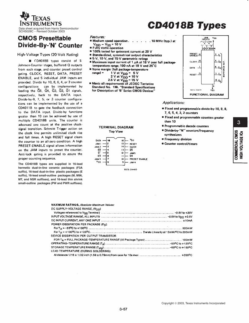
Data sheet acquired from Harris SemiconductorSCHS028C − Revised October 2003
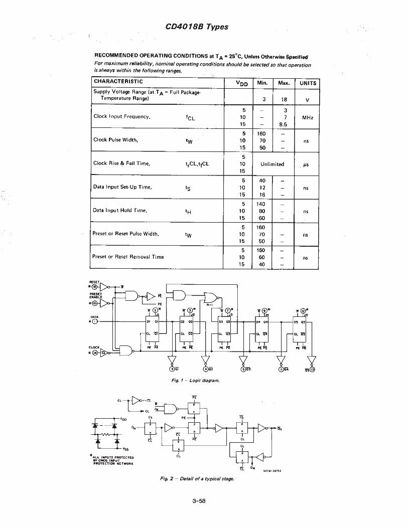
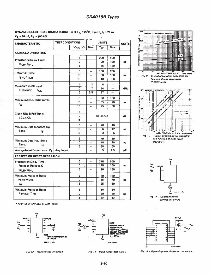
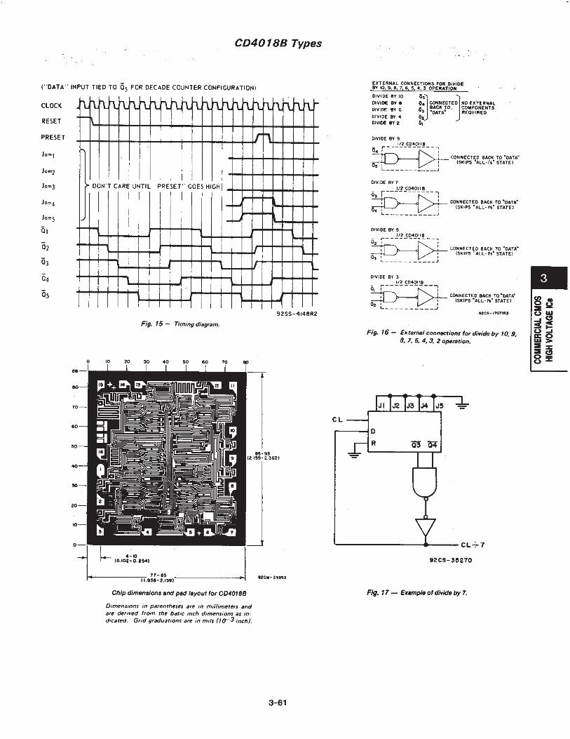
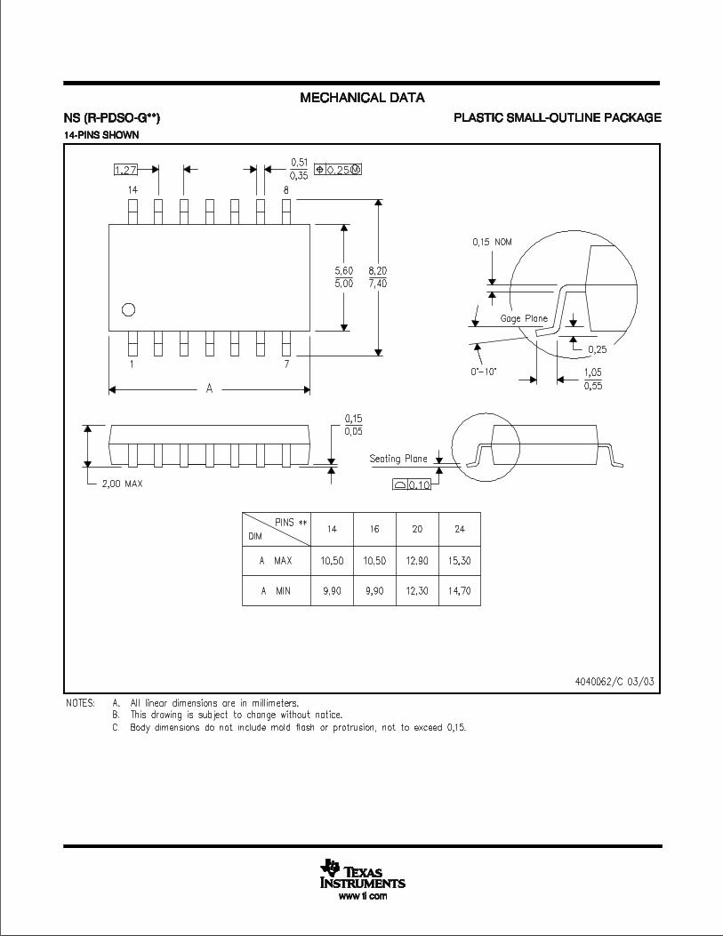
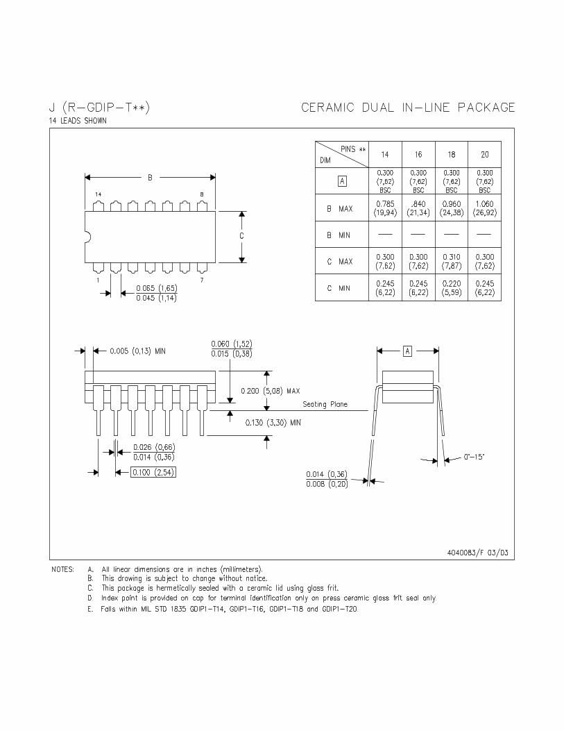
The CD4018B types are supplied in 16-leadhermetic dual-in-line ceramic packages (F3Asuffix), 16-lead dual-in-line plastic packages (Esuffix), 16-lead small-outline packages (M, M96,MT, and NSR suffixes), and 16-lead thin shrinksmall-outline packages (PW and PWR suffixes).
Copyright © 2003, Texas Instruments Incorporated

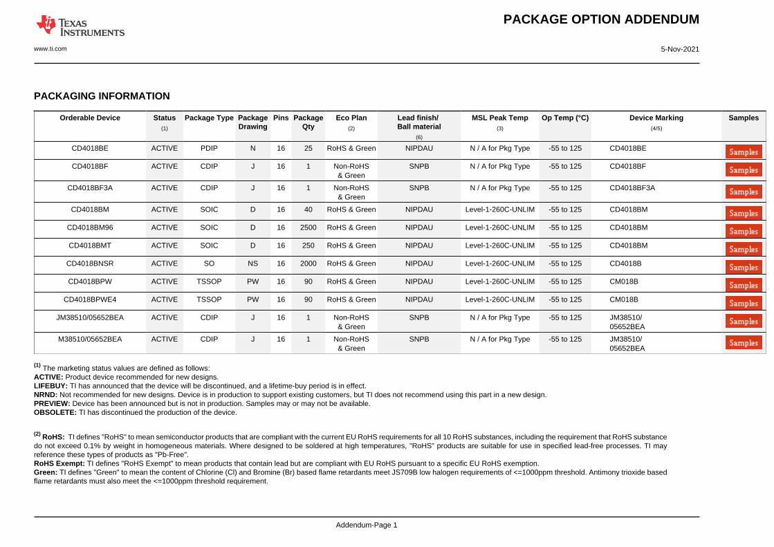
PACKAGE OPTION ADDENDUM
www.ti.com 5-Nov-2021
Addendum-Page 1
PACKAGING INFORMATION
Orderable Device Status(1)
Package Type PackageDrawing
Pins PackageQty
Eco Plan(2)
Lead finish/Ball material
(6)
MSL Peak Temp(3)
Op Temp (°C) Device Marking(4/5)
Samples
CD4018BE ACTIVE PDIP N 16 25 RoHS & Green NIPDAU N / A for Pkg Type -55 to 125 CD4018BE
CD4018BF ACTIVE CDIP J 16 1 Non-RoHS& Green
SNPB N / A for Pkg Type -55 to 125 CD4018BF
CD4018BF3A ACTIVE CDIP J 16 1 Non-RoHS& Green
SNPB N / A for Pkg Type -55 to 125 CD4018BF3A
CD4018BM ACTIVE SOIC D 16 40 RoHS & Green NIPDAU Level-1-260C-UNLIM -55 to 125 CD4018BM
CD4018BM96 ACTIVE SOIC D 16 2500 RoHS & Green NIPDAU Level-1-260C-UNLIM -55 to 125 CD4018BM
CD4018BMT ACTIVE SOIC D 16 250 RoHS & Green NIPDAU Level-1-260C-UNLIM -55 to 125 CD4018BM
CD4018BNSR ACTIVE SO NS 16 2000 RoHS & Green NIPDAU Level-1-260C-UNLIM -55 to 125 CD4018B
CD4018BPW ACTIVE TSSOP PW 16 90 RoHS & Green NIPDAU Level-1-260C-UNLIM -55 to 125 CM018B
CD4018BPWE4 ACTIVE TSSOP PW 16 90 RoHS & Green NIPDAU Level-1-260C-UNLIM -55 to 125 CM018B
JM38510/05652BEA ACTIVE CDIP J 16 1 Non-RoHS& Green
SNPB N / A for Pkg Type -55 to 125 JM38510/05652BEA
M38510/05652BEA ACTIVE CDIP J 16 1 Non-RoHS& Green
SNPB N / A for Pkg Type -55 to 125 JM38510/05652BEA
(1) The marketing status values are defined as follows:ACTIVE: Product device recommended for new designs.LIFEBUY: TI has announced that the device will be discontinued, and a lifetime-buy period is in effect.NRND: Not recommended for new designs. Device is in production to support existing customers, but TI does not recommend using this part in a new design.PREVIEW: Device has been announced but is not in production. Samples may or may not be available.OBSOLETE: TI has discontinued the production of the device.
(2) RoHS: TI defines "RoHS" to mean semiconductor products that are compliant with the current EU RoHS requirements for all 10 RoHS substances, including the requirement that RoHS substancedo not exceed 0.1% by weight in homogeneous materials. Where designed to be soldered at high temperatures, "RoHS" products are suitable for use in specified lead-free processes. TI mayreference these types of products as "Pb-Free".RoHS Exempt: TI defines "RoHS Exempt" to mean products that contain lead but are compliant with EU RoHS pursuant to a specific EU RoHS exemption.Green: TI defines "Green" to mean the content of Chlorine (Cl) and Bromine (Br) based flame retardants meet JS709B low halogen requirements of <=1000ppm threshold. Antimony trioxide basedflame retardants must also meet the <=1000ppm threshold requirement.
PACKAGE OPTION ADDENDUM
www.ti.com 5-Nov-2021
Addendum-Page 2
(3) MSL, Peak Temp. - The Moisture Sensitivity Level rating according to the JEDEC industry standard classifications, and peak solder temperature.
(4) There may be additional marking, which relates to the logo, the lot trace code information, or the environmental category on the device.
(5) Multiple Device Markings will be inside parentheses. Only one Device Marking contained in parentheses and separated by a "~" will appear on a device. If a line is indented then it is a continuationof the previous line and the two combined represent the entire Device Marking for that device.
(6) Lead finish/Ball material - Orderable Devices may have multiple material finish options. Finish options are separated by a vertical ruled line. Lead finish/Ball material values may wrap to twolines if the finish value exceeds the maximum column width.
Important Information and Disclaimer:The information provided on this page represents TI's knowledge and belief as of the date that it is provided. TI bases its knowledge and belief on informationprovided by third parties, and makes no representation or warranty as to the accuracy of such information. Efforts are underway to better integrate information from third parties. TI has taken andcontinues to take reasonable steps to provide representative and accurate information but may not have conducted destructive testing or chemical analysis on incoming materials and chemicals.TI and TI suppliers consider certain information to be proprietary, and thus CAS numbers and other limited information may not be available for release.
In no event shall TI's liability arising out of such information exceed the total purchase price of the TI part(s) at issue in this document sold by TI to Customer on an annual basis.
OTHER QUALIFIED VERSIONS OF CD4018B, CD4018B-MIL :
• Catalog : CD4018B
• Military : CD4018B-MIL
NOTE: Qualified Version Definitions:
• Catalog - TI's standard catalog product
• Military - QML certified for Military and Defense Applications
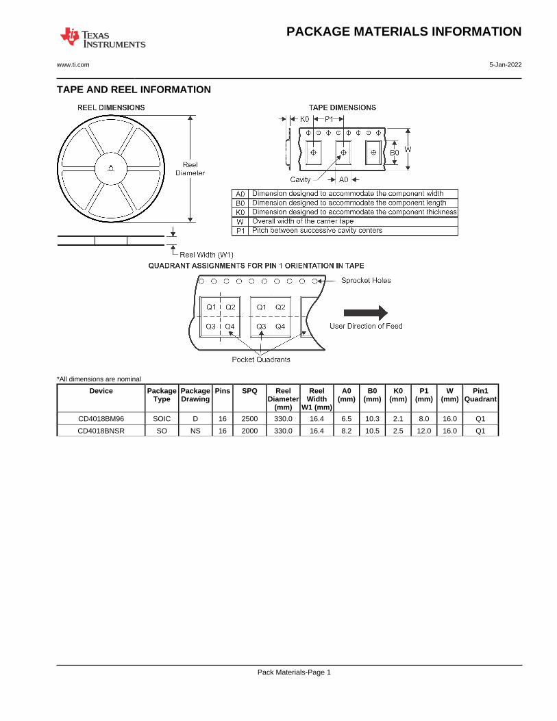
TAPE AND REEL INFORMATION
*All dimensions are nominal
Device PackageType
PackageDrawing
Pins SPQ ReelDiameter
(mm)
ReelWidth
W1 (mm)
A0(mm)
B0(mm)
K0(mm)
P1(mm)
W(mm)
Pin1Quadrant
CD4018BM96 SOIC D 16 2500 330.0 16.4 6.5 10.3 2.1 8.0 16.0 Q1
CD4018BNSR SO NS 16 2000 330.0 16.4 8.2 10.5 2.5 12.0 16.0 Q1
PACKAGE MATERIALS INFORMATION
www.ti.com 5-Jan-2022
Pack Materials-Page 1

*All dimensions are nominal
Device Package Type Package Drawing Pins SPQ Length (mm) Width (mm) Height (mm)
CD4018BM96 SOIC D 16 2500 340.5 336.1 32.0
CD4018BNSR SO NS 16 2000 853.0 449.0 35.0
PACKAGE MATERIALS INFORMATION
www.ti.com 5-Jan-2022
Pack Materials-Page 2
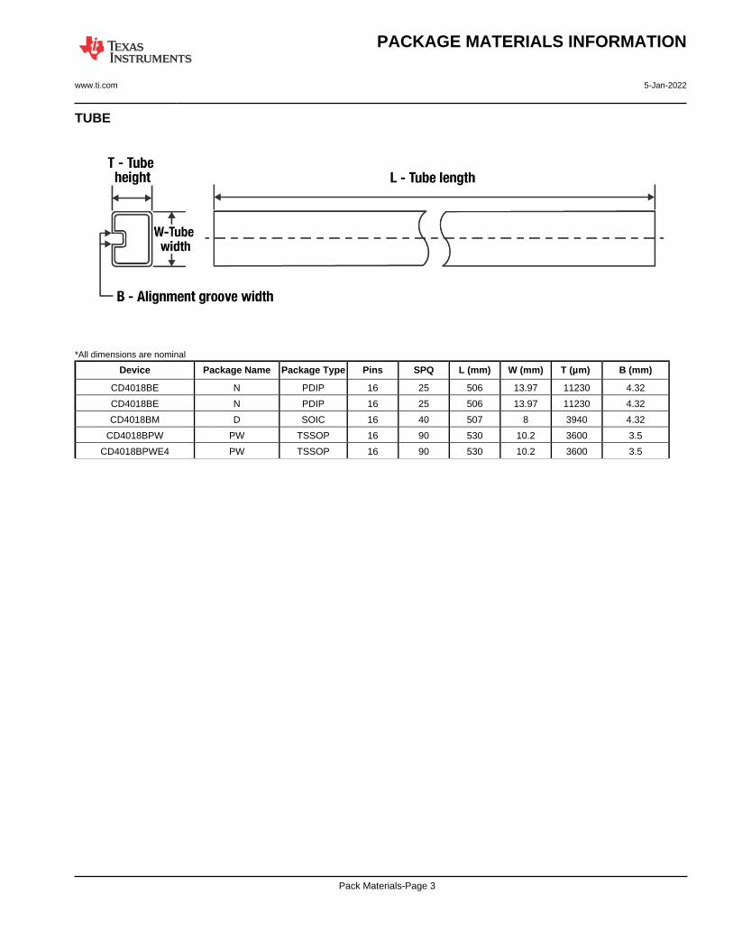
TUBE
*All dimensions are nominal
Device Package Name Package Type Pins SPQ L (mm) W (mm) T (µm) B (mm)
CD4018BE N PDIP 16 25 506 13.97 11230 4.32
CD4018BE N PDIP 16 25 506 13.97 11230 4.32
CD4018BM D SOIC 16 40 507 8 3940 4.32
CD4018BPW PW TSSOP 16 90 530 10.2 3600 3.5
CD4018BPWE4 PW TSSOP 16 90 530 10.2 3600 3.5
PACKAGE MATERIALS INFORMATION
www.ti.com 5-Jan-2022
Pack Materials-Page 3
www.ti.com
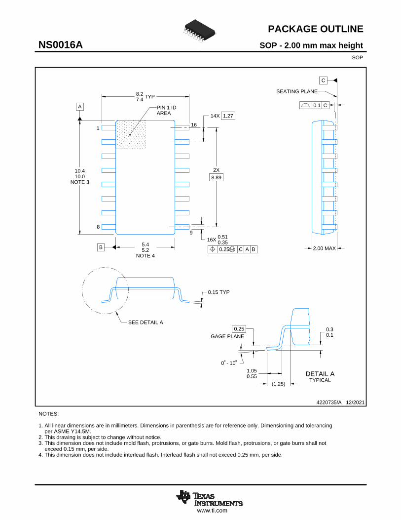
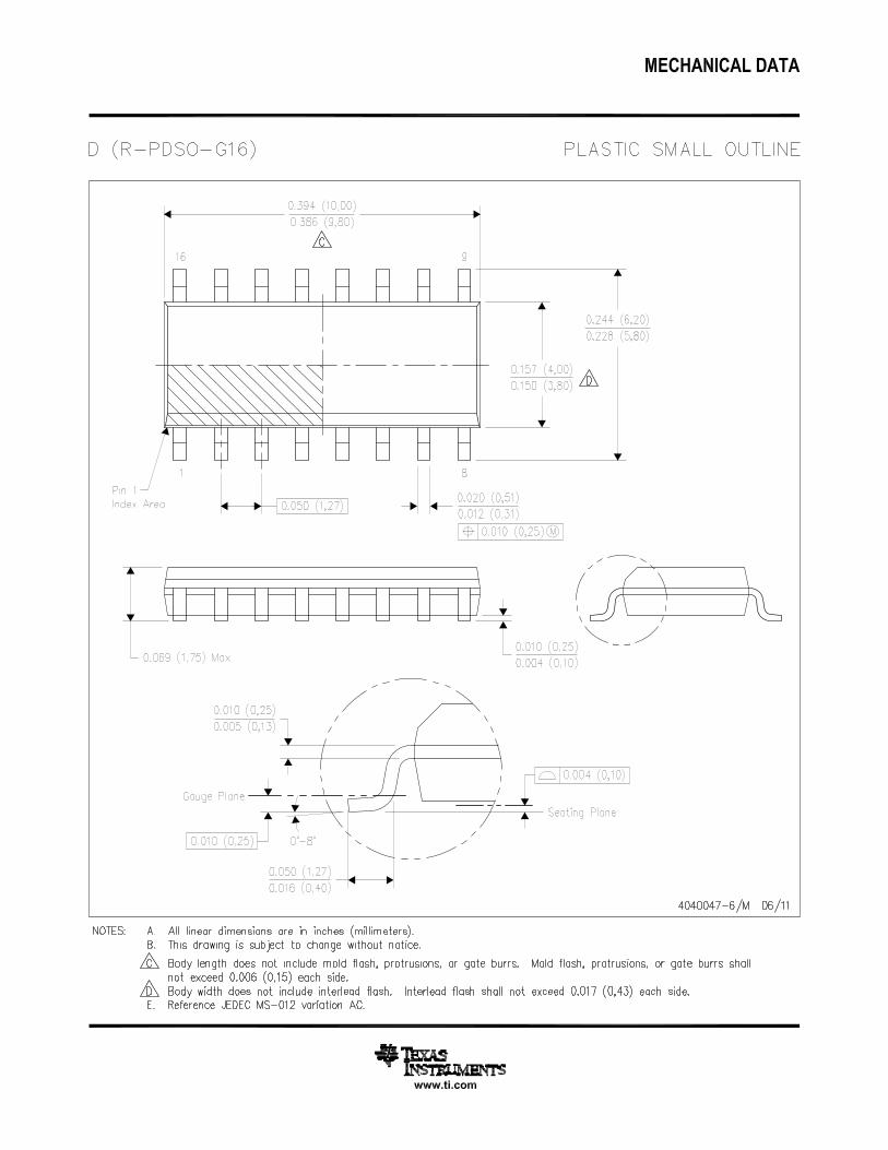
PACKAGE OUTLINE
C
8.27.4 TYP
14X 1.27
16X 0.510.35
2X8.89
0.15 TYP
0 - 10
0.30.1
2.00 MAX
(1.25)
0.25GAGE PLANE
1.050.55
A
10.410.0
NOTE 3
B 5.45.2
NOTE 4
4220735/A 12/2021
SOP - 2.00 mm max heightNS0016ASOP
NOTES: 1. All linear dimensions are in millimeters. Dimensions in parenthesis are for reference only. Dimensioning and tolerancing per ASME Y14.5M. 2. This drawing is subject to change without notice. 3. This dimension does not include mold flash, protrusions, or gate burrs. Mold flash, protrusions, or gate burrs shall not exceed 0.15 mm, per side. 4. This dimension does not include interlead flash. Interlead flash shall not exceed 0.25 mm, per side.
1 16
0.25 C A B
98
PIN 1 IDAREA
SEATING PLANE
0.1 C
SEE DETAIL A
DETAIL ATYPICAL
SCALE 1.500
www.ti.com
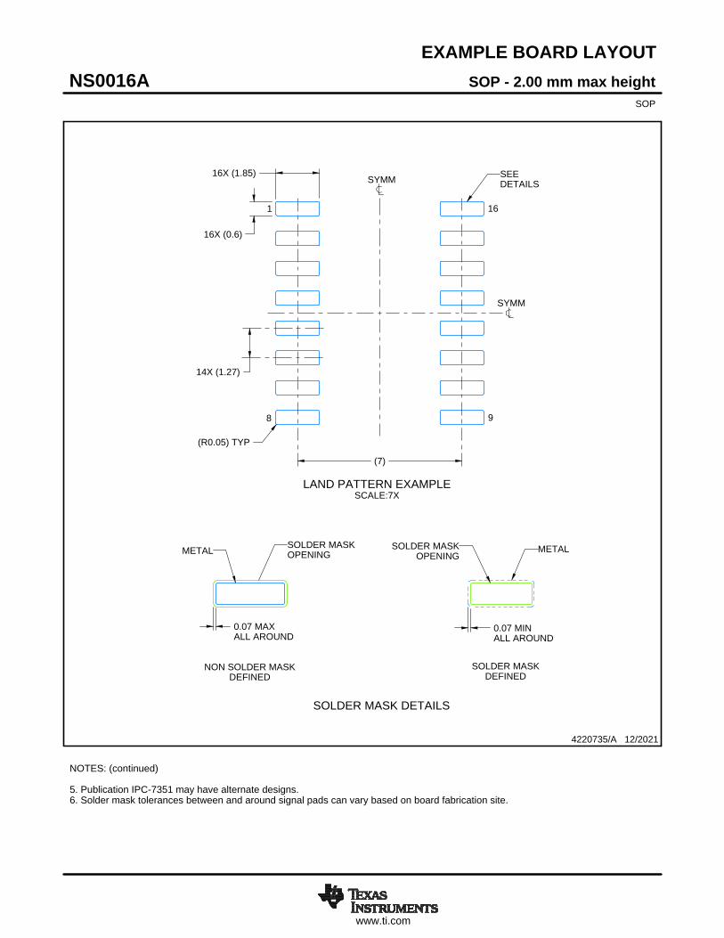
EXAMPLE BOARD LAYOUT
0.07 MAXALL AROUND
0.07 MINALL AROUND
14X (1.27)
(R0.05) TYP
(7)
16X (1.85)
16X (0.6)
4220735/A 12/2021
SOP - 2.00 mm max heightNS0016ASOP
NOTES: (continued) 5. Publication IPC-7351 may have alternate designs. 6. Solder mask tolerances between and around signal pads can vary based on board fabrication site.
METAL SOLDER MASKOPENING
NON SOLDER MASKDEFINED
SOLDER MASK DETAILS
OPENINGSOLDER MASK METAL
SOLDER MASKDEFINED
LAND PATTERN EXAMPLESCALE:7X
SYMM
1
8 9
16
SEEDETAILS
SYMM

www.ti.com
EXAMPLE STENCIL DESIGN
(7)(R0.05) TYP
16X (1.85)
16X (0.6)
14X (1.27)
4220735/A 12/2021
SOP - 2.00 mm max heightNS0016ASOP
NOTES: (continued) 7. Laser cutting apertures with trapezoidal walls and rounded corners may offer better paste release. IPC-7525 may have alternate design recommendations. 8. Board assembly site may have different recommendations for stencil design.
SOLDER PASTE EXAMPLEBASED ON 0.125 mm THICK STENCIL
SCALE:7X
SYMM
SYMM
1
8 9
16

www.ti.com
PACKAGE OUTLINE
C
14X 0.65
2X4.55
16X 0.300.19
TYP6.66.2
1.2 MAX
0.150.05
0.25GAGE PLANE
-80
BNOTE 4
4.54.3
A
NOTE 3
5.14.9
0.750.50
(0.15) TYP
TSSOP - 1.2 mm max heightPW0016ASMALL OUTLINE PACKAGE
4220204/A 02/2017
1
89
16
0.1 C A B
PIN 1 INDEX AREA
SEE DETAIL A
0.1 C
NOTES: 1. All linear dimensions are in millimeters. Any dimensions in parenthesis are for reference only. Dimensioning and tolerancing per ASME Y14.5M. 2. This drawing is subject to change without notice. 3. This dimension does not include mold flash, protrusions, or gate burrs. Mold flash, protrusions, or gate burrs shall not exceed 0.15 mm per side. 4. This dimension does not include interlead flash. Interlead flash shall not exceed 0.25 mm per side.5. Reference JEDEC registration MO-153.
SEATINGPLANE
A 20DETAIL ATYPICAL
SCALE 2.500
www.ti.com
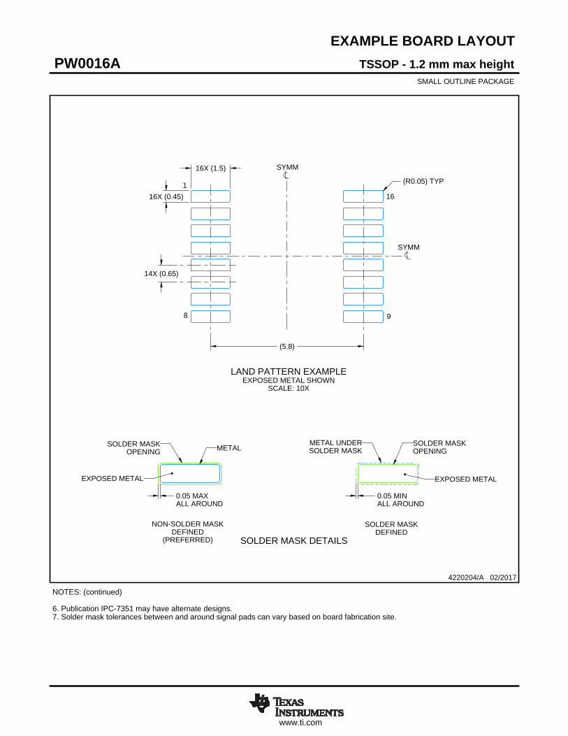
EXAMPLE BOARD LAYOUT
0.05 MAXALL AROUND
0.05 MINALL AROUND
16X (1.5)
16X (0.45)
14X (0.65)
(5.8)
(R0.05) TYP
TSSOP - 1.2 mm max heightPW0016ASMALL OUTLINE PACKAGE
4220204/A 02/2017
NOTES: (continued) 6. Publication IPC-7351 may have alternate designs. 7. Solder mask tolerances between and around signal pads can vary based on board fabrication site.
LAND PATTERN EXAMPLEEXPOSED METAL SHOWN
SCALE: 10X
SYMM
SYMM
1
8 9
16
15.000
METALSOLDER MASKOPENING
METAL UNDERSOLDER MASK
SOLDER MASKOPENING
EXPOSED METALEXPOSED METAL
SOLDER MASK DETAILS
NON-SOLDER MASKDEFINED
(PREFERRED)
SOLDER MASKDEFINED

www.ti.com
EXAMPLE STENCIL DESIGN
16X (1.5)
16X (0.45)
14X (0.65)
(5.8)
(R0.05) TYP
TSSOP - 1.2 mm max heightPW0016ASMALL OUTLINE PACKAGE
4220204/A 02/2017
NOTES: (continued) 8. Laser cutting apertures with trapezoidal walls and rounded corners may offer better paste release. IPC-7525 may have alternate design recommendations. 9. Board assembly site may have different recommendations for stencil design.
SOLDER PASTE EXAMPLEBASED ON 0.125 mm THICK STENCIL
SCALE: 10X
SYMM
SYMM
1
8 9
16

IMPORTANT NOTICE AND DISCLAIMERTI PROVIDES TECHNICAL AND RELIABILITY DATA (INCLUDING DATA SHEETS), DESIGN RESOURCES (INCLUDING REFERENCE DESIGNS), APPLICATION OR OTHER DESIGN ADVICE, WEB TOOLS, SAFETY INFORMATION, AND OTHER RESOURCES “AS IS” AND WITH ALL FAULTS, AND DISCLAIMS ALL WARRANTIES, EXPRESS AND IMPLIED, INCLUDING WITHOUT LIMITATION ANY IMPLIED WARRANTIES OF MERCHANTABILITY, FITNESS FOR A PARTICULAR PURPOSE OR NON-INFRINGEMENT OF THIRD PARTY INTELLECTUAL PROPERTY RIGHTS.These resources are intended for skilled developers designing with TI products. You are solely responsible for (1) selecting the appropriate TI products for your application, (2) designing, validating and testing your application, and (3) ensuring your application meets applicable standards, and any other safety, security, regulatory or other requirements.These resources are subject to change without notice. TI grants you permission to use these resources only for development of an application that uses the TI products described in the resource. Other reproduction and display of these resources is prohibited. No license is granted to any other TI intellectual property right or to any third party intellectual property right. TI disclaims responsibility for, and you will fully indemnify TI and its representatives against, any claims, damages, costs, losses, and liabilities arising out of your use of these resources.TI’s products are provided subject to TI’s Terms of Sale or other applicable terms available either on ti.com or provided in conjunction with such TI products. TI’s provision of these resources does not expand or otherwise alter TI’s applicable warranties or warranty disclaimers for TI products.TI objects to and rejects any additional or different terms you may have proposed. IMPORTANT NOTICE
Mailing Address: Texas Instruments, Post Office Box 655303, Dallas, Texas 75265Copyright © 2022, Texas Instruments Incorporated


![Data sheet acquired from Harris Semiconductor SCHS033C ......CD4028B TYPES datasheet (Rev. C) Author Texas Instruments, Incorporated [SCHS033,C ] Subject Data Sheet Keywords SCHS033C,SCHS033](https://img.pdfslide.us/doc/110x75/60ddf1d45e033a68fe1f0457/data-sheet-acquired-from-harris-semiconductor-schs033c-cd4028b-types-datasheet.jpg)