Embed Size (px)
Citation preview
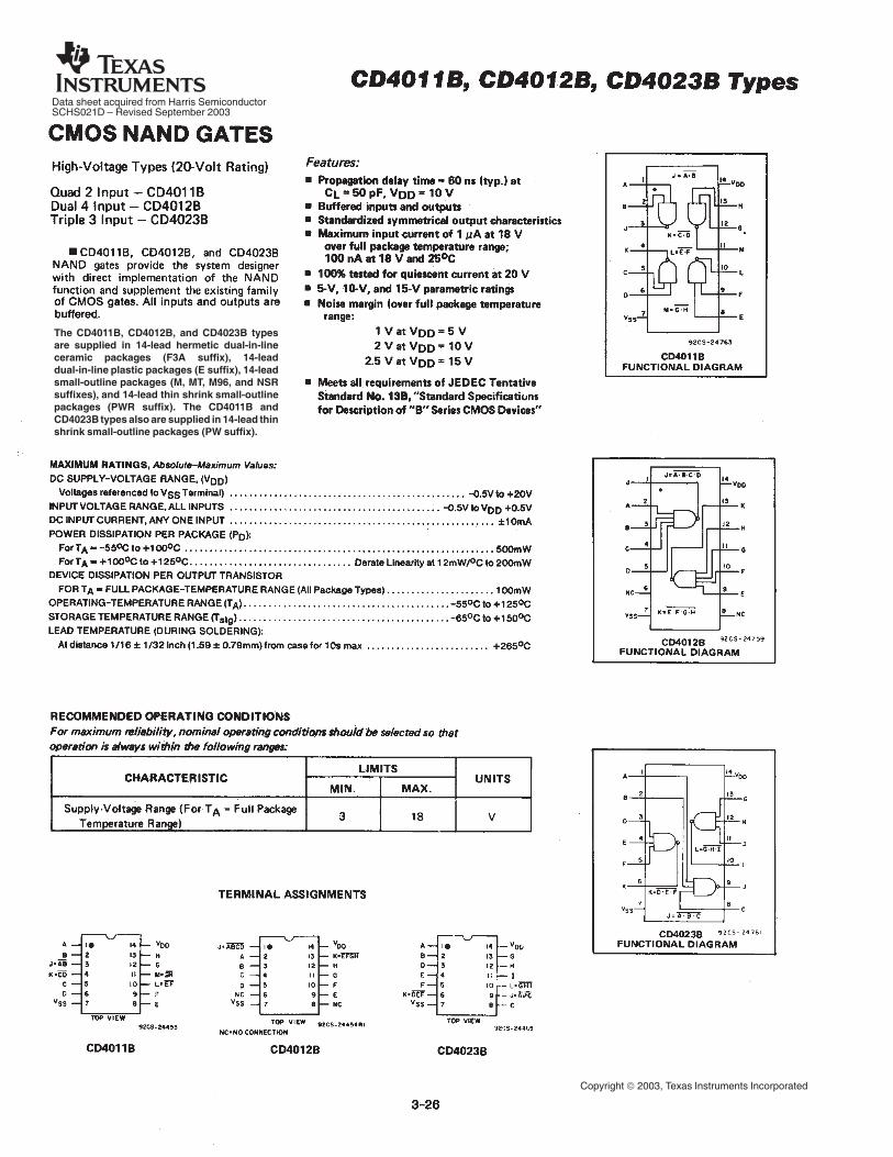
Data sheet acquired from Harris SemiconductorSCHS021D – Revised September 2003
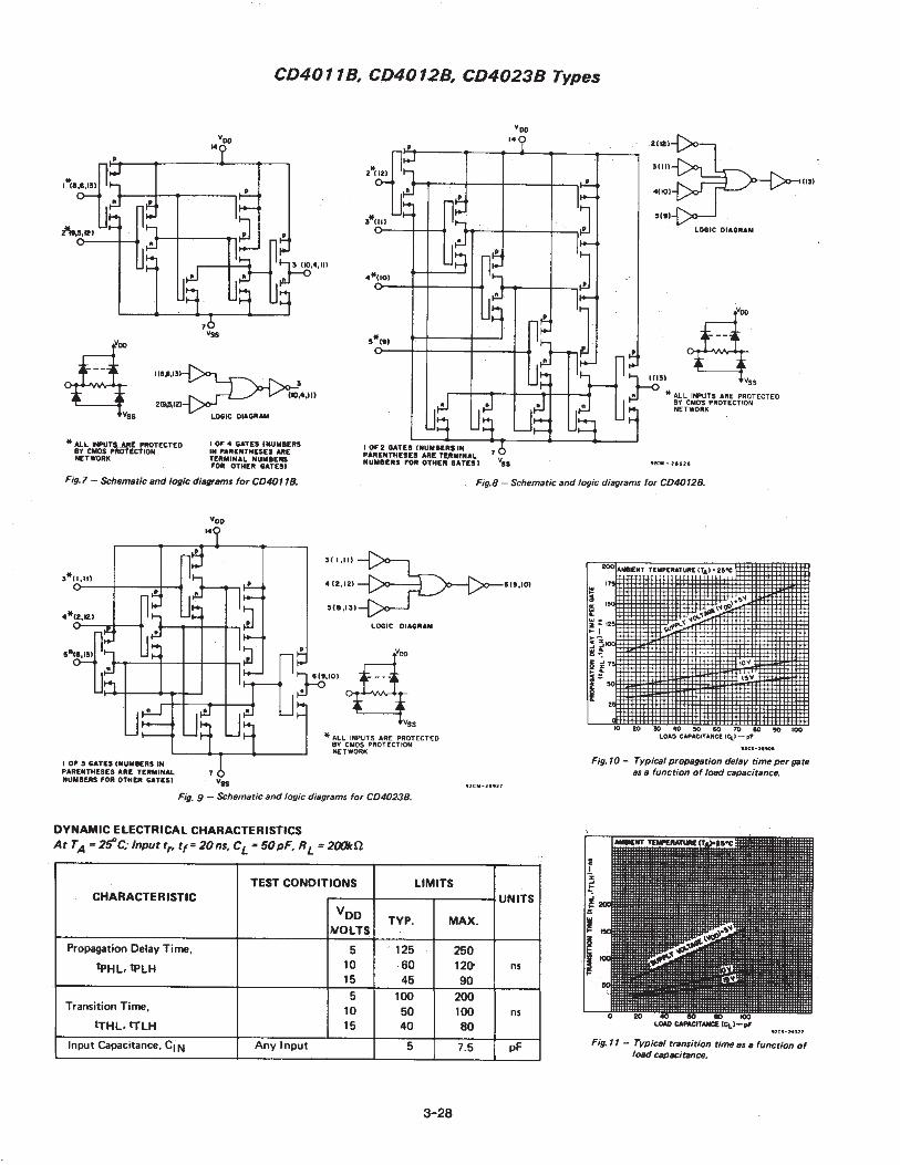
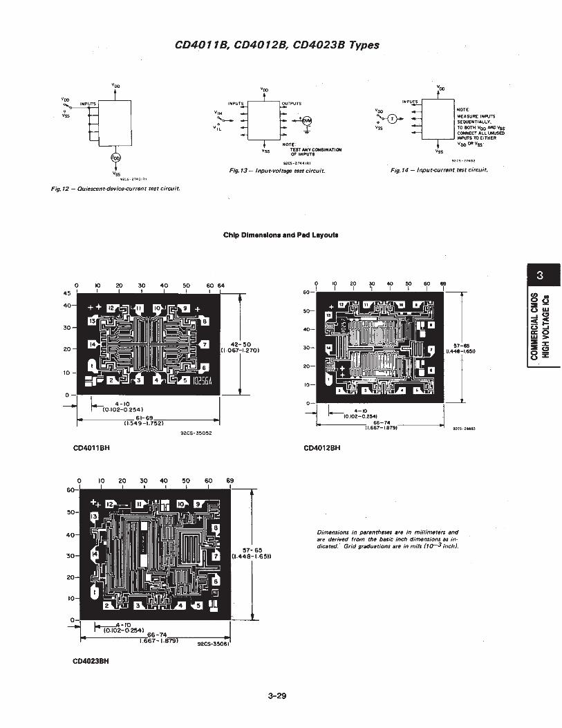
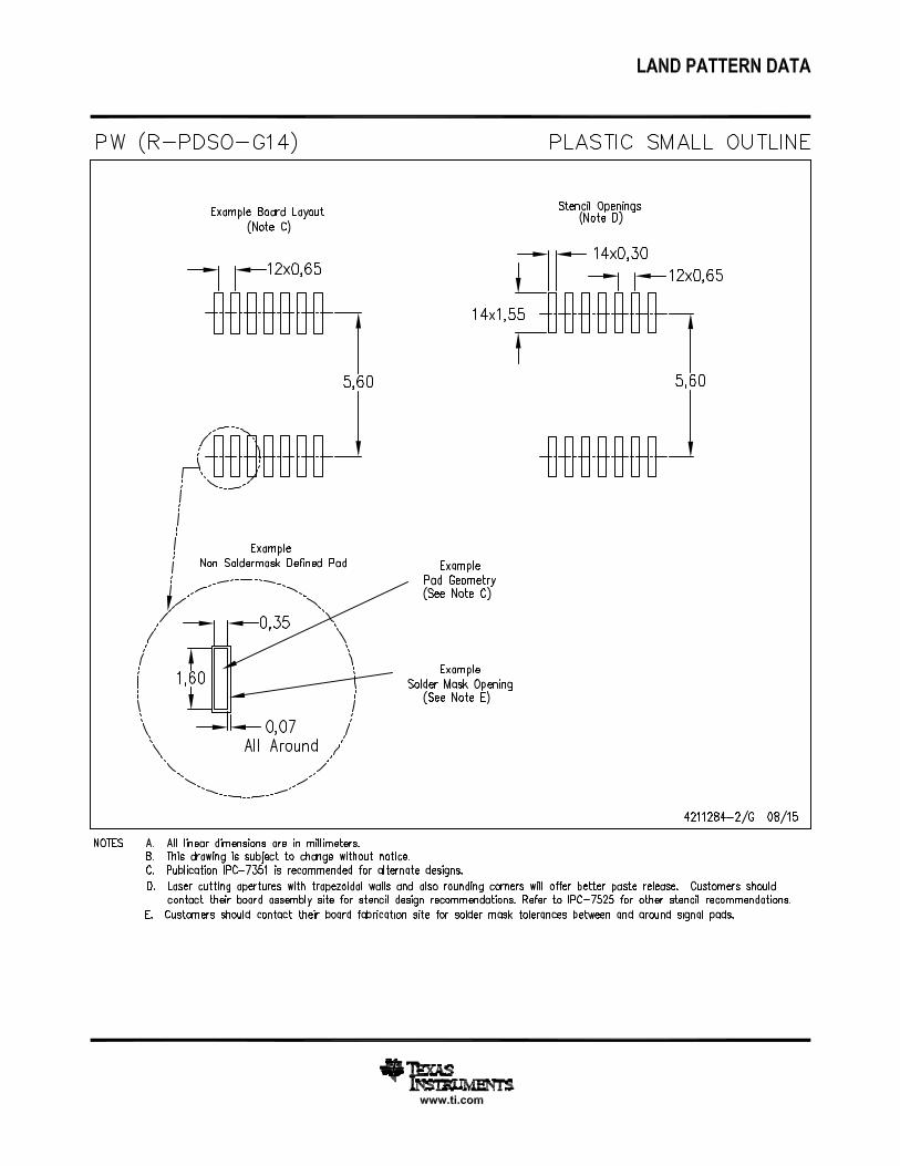
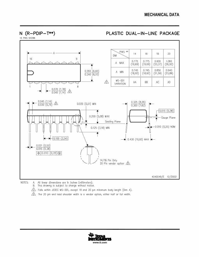
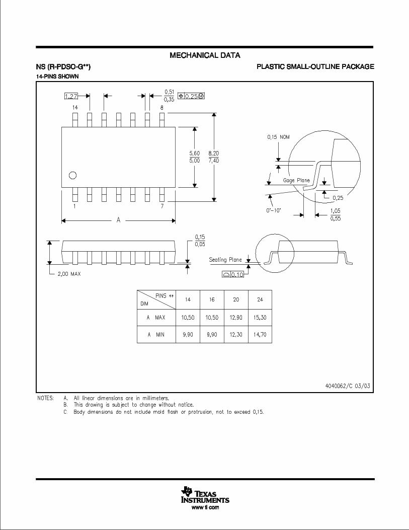
The CD4011B, CD4012B, and CD4023B typesare supplied in 14-lead hermetic dual-in-lineceramic packages (F3A suffix), 14-leaddual-in-line plastic packages (E suffix), 14-leadsmall-outline packages (M, MT, M96, and NSRsuffixes), and 14-lead thin shrink small-outlinepackages (PWR suffix). The CD4011B andCD4023B types also are supplied in 14-lead thinshrink small-outline packages (PW suffix).
Copyright © 2003, Texas Instruments Incorporated

PACKAGE OPTION ADDENDUM
www.ti.com 17-Mar-2017
Addendum-Page 1
PACKAGING INFORMATION
Orderable Device Status(1)
Package Type PackageDrawing
Pins PackageQty
Eco Plan(2)
Lead/Ball Finish(6)
MSL Peak Temp(3)
Op Temp (°C) Device Marking(4/5)
Samples
CD4011BE ACTIVE PDIP N 14 25 Pb-Free(RoHS)
CU NIPDAU N / A for Pkg Type -55 to 125 CD4011BE
CD4011BEE4 ACTIVE PDIP N 14 25 Pb-Free(RoHS)
CU NIPDAU N / A for Pkg Type -55 to 125 CD4011BE
CD4011BF ACTIVE CDIP J 14 1 TBD A42 N / A for Pkg Type -55 to 125 CD4011BF
CD4011BF3A ACTIVE CDIP J 14 1 TBD A42 N / A for Pkg Type -55 to 125 CD4011BF3A
CD4011BM ACTIVE SOIC D 14 50 Green (RoHS& no Sb/Br)
CU NIPDAU Level-1-260C-UNLIM -55 to 125 CD4011BM
CD4011BM96 ACTIVE SOIC D 14 2500 Green (RoHS& no Sb/Br)
CU NIPDAU Level-1-260C-UNLIM -55 to 125 CD4011BM
CD4011BM96E4 ACTIVE SOIC D 14 2500 Green (RoHS& no Sb/Br)
CU NIPDAU Level-1-260C-UNLIM -55 to 125 CD4011BM
CD4011BM96G4 ACTIVE SOIC D 14 2500 Green (RoHS& no Sb/Br)
CU NIPDAU Level-1-260C-UNLIM -55 to 125 CD4011BM
CD4011BME4 ACTIVE SOIC D 14 50 Green (RoHS& no Sb/Br)
CU NIPDAU Level-1-260C-UNLIM -55 to 125 CD4011BM
CD4011BMT ACTIVE SOIC D 14 250 Green (RoHS& no Sb/Br)
CU NIPDAU Level-1-260C-UNLIM -55 to 125 CD4011BM
CD4011BNSR ACTIVE SO NS 14 2000 Green (RoHS& no Sb/Br)
CU NIPDAU Level-1-260C-UNLIM -55 to 125 CD4011B
CD4011BNSRG4 ACTIVE SO NS 14 2000 Green (RoHS& no Sb/Br)
CU NIPDAU Level-1-260C-UNLIM -55 to 125 CD4011B
CD4011BPW ACTIVE TSSOP PW 14 90 Green (RoHS& no Sb/Br)
CU NIPDAU Level-1-260C-UNLIM -55 to 125 CM011B
CD4011BPWE4 ACTIVE TSSOP PW 14 90 Green (RoHS& no Sb/Br)
CU NIPDAU Level-1-260C-UNLIM -55 to 125 CM011B
CD4011BPWR ACTIVE TSSOP PW 14 2000 Green (RoHS& no Sb/Br)
CU NIPDAU Level-1-260C-UNLIM -55 to 125 CM011B
CD4011BPWRG4 ACTIVE TSSOP PW 14 2000 Green (RoHS& no Sb/Br)
CU NIPDAU Level-1-260C-UNLIM -55 to 125 CM011B
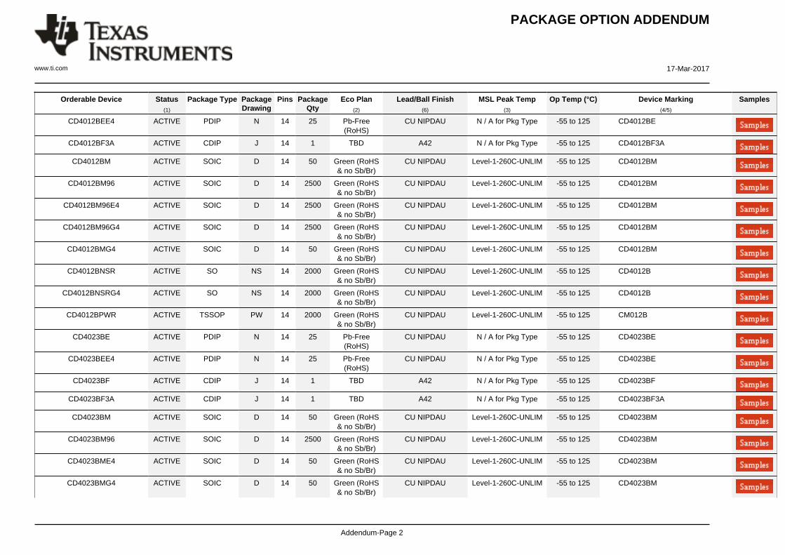
CD4012BE ACTIVE PDIP N 14 25 Pb-Free(RoHS)
CU NIPDAU N / A for Pkg Type -55 to 125 CD4012BE
PACKAGE OPTION ADDENDUM
www.ti.com 17-Mar-2017
Addendum-Page 2
Orderable Device Status(1)
Package Type PackageDrawing
Pins PackageQty
Eco Plan(2)
Lead/Ball Finish(6)
MSL Peak Temp(3)
Op Temp (°C) Device Marking(4/5)
Samples
CD4012BEE4 ACTIVE PDIP N 14 25 Pb-Free(RoHS)
CU NIPDAU N / A for Pkg Type -55 to 125 CD4012BE
CD4012BF3A ACTIVE CDIP J 14 1 TBD A42 N / A for Pkg Type -55 to 125 CD4012BF3A
CD4012BM ACTIVE SOIC D 14 50 Green (RoHS& no Sb/Br)
CU NIPDAU Level-1-260C-UNLIM -55 to 125 CD4012BM
CD4012BM96 ACTIVE SOIC D 14 2500 Green (RoHS& no Sb/Br)
CU NIPDAU Level-1-260C-UNLIM -55 to 125 CD4012BM
CD4012BM96E4 ACTIVE SOIC D 14 2500 Green (RoHS& no Sb/Br)
CU NIPDAU Level-1-260C-UNLIM -55 to 125 CD4012BM
CD4012BM96G4 ACTIVE SOIC D 14 2500 Green (RoHS& no Sb/Br)
CU NIPDAU Level-1-260C-UNLIM -55 to 125 CD4012BM
CD4012BMG4 ACTIVE SOIC D 14 50 Green (RoHS& no Sb/Br)
CU NIPDAU Level-1-260C-UNLIM -55 to 125 CD4012BM
CD4012BNSR ACTIVE SO NS 14 2000 Green (RoHS& no Sb/Br)
CU NIPDAU Level-1-260C-UNLIM -55 to 125 CD4012B
CD4012BNSRG4 ACTIVE SO NS 14 2000 Green (RoHS& no Sb/Br)
CU NIPDAU Level-1-260C-UNLIM -55 to 125 CD4012B
CD4012BPWR ACTIVE TSSOP PW 14 2000 Green (RoHS& no Sb/Br)
CU NIPDAU Level-1-260C-UNLIM -55 to 125 CM012B
CD4023BE ACTIVE PDIP N 14 25 Pb-Free(RoHS)
CU NIPDAU N / A for Pkg Type -55 to 125 CD4023BE
CD4023BEE4 ACTIVE PDIP N 14 25 Pb-Free(RoHS)
CU NIPDAU N / A for Pkg Type -55 to 125 CD4023BE
CD4023BF ACTIVE CDIP J 14 1 TBD A42 N / A for Pkg Type -55 to 125 CD4023BF
CD4023BF3A ACTIVE CDIP J 14 1 TBD A42 N / A for Pkg Type -55 to 125 CD4023BF3A
CD4023BM ACTIVE SOIC D 14 50 Green (RoHS& no Sb/Br)
CU NIPDAU Level-1-260C-UNLIM -55 to 125 CD4023BM
CD4023BM96 ACTIVE SOIC D 14 2500 Green (RoHS& no Sb/Br)
CU NIPDAU Level-1-260C-UNLIM -55 to 125 CD4023BM
CD4023BME4 ACTIVE SOIC D 14 50 Green (RoHS& no Sb/Br)
CU NIPDAU Level-1-260C-UNLIM -55 to 125 CD4023BM
CD4023BMG4 ACTIVE SOIC D 14 50 Green (RoHS& no Sb/Br)
CU NIPDAU Level-1-260C-UNLIM -55 to 125 CD4023BM

PACKAGE OPTION ADDENDUM
www.ti.com 17-Mar-2017
Addendum-Page 3
Orderable Device Status(1)
Package Type PackageDrawing
Pins PackageQty
Eco Plan(2)
Lead/Ball Finish(6)
MSL Peak Temp(3)
Op Temp (°C) Device Marking(4/5)
Samples
CD4023BMT ACTIVE SOIC D 14 250 Green (RoHS& no Sb/Br)
CU NIPDAU Level-1-260C-UNLIM -55 to 125 CD4023BM
CD4023BMTE4 ACTIVE SOIC D 14 250 Green (RoHS& no Sb/Br)
CU NIPDAU Level-1-260C-UNLIM -55 to 125 CD4023BM
CD4023BNSR ACTIVE SO NS 14 2000 Green (RoHS& no Sb/Br)
CU NIPDAU Level-1-260C-UNLIM -55 to 125 CD4023B
CD4023BNSRG4 ACTIVE SO NS 14 2000 Green (RoHS& no Sb/Br)
CU NIPDAU Level-1-260C-UNLIM -55 to 125 CD4023B
CD4023BPW ACTIVE TSSOP PW 14 90 Green (RoHS& no Sb/Br)
CU NIPDAU Level-1-260C-UNLIM -55 to 125 CM023B
CD4023BPWR ACTIVE TSSOP PW 14 2000 Green (RoHS& no Sb/Br)
CU NIPDAU Level-1-260C-UNLIM -55 to 125 CM023B
JM38510/05051BCA ACTIVE CDIP J 14 1 TBD A42 N / A for Pkg Type -55 to 125 JM38510/05051BCA
JM38510/05052BCA ACTIVE CDIP J 14 1 TBD A42 N / A for Pkg Type -55 to 125 JM38510/05052BCA
JM38510/05053BCA ACTIVE CDIP J 14 1 TBD A42 N / A for Pkg Type -55 to 125 JM38510/05053BCA
M38510/05051BCA ACTIVE CDIP J 14 1 TBD A42 N / A for Pkg Type -55 to 125 JM38510/05051BCA
M38510/05052BCA ACTIVE CDIP J 14 1 TBD A42 N / A for Pkg Type -55 to 125 JM38510/05052BCA
M38510/05053BCA ACTIVE CDIP J 14 1 TBD A42 N / A for Pkg Type -55 to 125 JM38510/05053BCA
(1) The marketing status values are defined as follows:ACTIVE: Product device recommended for new designs.LIFEBUY: TI has announced that the device will be discontinued, and a lifetime-buy period is in effect.NRND: Not recommended for new designs. Device is in production to support existing customers, but TI does not recommend using this part in a new design.PREVIEW: Device has been announced but is not in production. Samples may or may not be available.OBSOLETE: TI has discontinued the production of the device.
(2) Eco Plan - The planned eco-friendly classification: Pb-Free (RoHS), Pb-Free (RoHS Exempt), or Green (RoHS & no Sb/Br) - please check http://www.ti.com/productcontent for the latest availabilityinformation and additional product content details.TBD: The Pb-Free/Green conversion plan has not been defined.Pb-Free (RoHS): TI's terms "Lead-Free" or "Pb-Free" mean semiconductor products that are compatible with the current RoHS requirements for all 6 substances, including the requirement thatlead not exceed 0.1% by weight in homogeneous materials. Where designed to be soldered at high temperatures, TI Pb-Free products are suitable for use in specified lead-free processes.
PACKAGE OPTION ADDENDUM
www.ti.com 17-Mar-2017
Addendum-Page 4
Pb-Free (RoHS Exempt): This component has a RoHS exemption for either 1) lead-based flip-chip solder bumps used between the die and package, or 2) lead-based die adhesive used betweenthe die and leadframe. The component is otherwise considered Pb-Free (RoHS compatible) as defined above.Green (RoHS & no Sb/Br): TI defines "Green" to mean Pb-Free (RoHS compatible), and free of Bromine (Br) and Antimony (Sb) based flame retardants (Br or Sb do not exceed 0.1% by weightin homogeneous material)
(3) MSL, Peak Temp. - The Moisture Sensitivity Level rating according to the JEDEC industry standard classifications, and peak solder temperature.
(4) There may be additional marking, which relates to the logo, the lot trace code information, or the environmental category on the device.
(5) Multiple Device Markings will be inside parentheses. Only one Device Marking contained in parentheses and separated by a "~" will appear on a device. If a line is indented then it is a continuationof the previous line and the two combined represent the entire Device Marking for that device.
(6) Lead/Ball Finish - Orderable Devices may have multiple material finish options. Finish options are separated by a vertical ruled line. Lead/Ball Finish values may wrap to two lines if the finishvalue exceeds the maximum column width.
Important Information and Disclaimer:The information provided on this page represents TI's knowledge and belief as of the date that it is provided. TI bases its knowledge and belief on informationprovided by third parties, and makes no representation or warranty as to the accuracy of such information. Efforts are underway to better integrate information from third parties. TI has taken andcontinues to take reasonable steps to provide representative and accurate information but may not have conducted destructive testing or chemical analysis on incoming materials and chemicals.TI and TI suppliers consider certain information to be proprietary, and thus CAS numbers and other limited information may not be available for release.
In no event shall TI's liability arising out of such information exceed the total purchase price of the TI part(s) at issue in this document sold by TI to Customer on an annual basis.
OTHER QUALIFIED VERSIONS OF CD4011B, CD4011B-MIL, CD4012B, CD4012B-MIL :
• Catalog: CD4011B, CD4012B
• Military: CD4011B-MIL, CD4012B-MIL
NOTE: Qualified Version Definitions:
• Catalog - TI's standard catalog product
• Military - QML certified for Military and Defense Applications
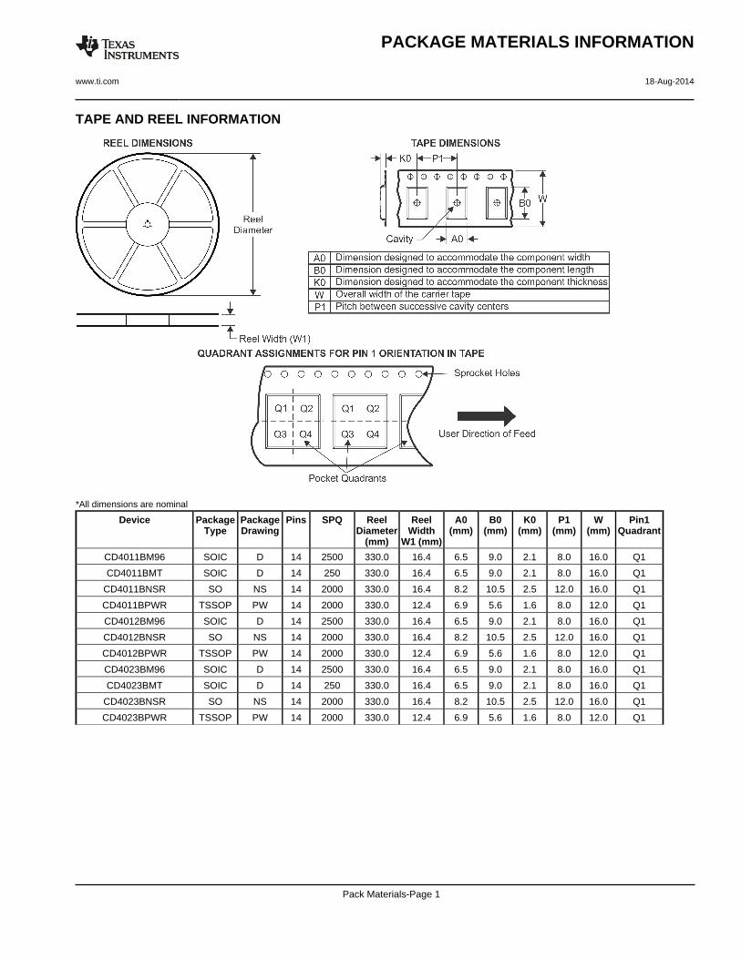
TAPE AND REEL INFORMATION
*All dimensions are nominal
Device PackageType
PackageDrawing
Pins SPQ ReelDiameter
(mm)
ReelWidth
W1 (mm)
A0(mm)
B0(mm)
K0(mm)
P1(mm)
W(mm)
Pin1Quadrant
CD4011BM96 SOIC D 14 2500 330.0 16.4 6.5 9.0 2.1 8.0 16.0 Q1
CD4011BMT SOIC D 14 250 330.0 16.4 6.5 9.0 2.1 8.0 16.0 Q1
CD4011BNSR SO NS 14 2000 330.0 16.4 8.2 10.5 2.5 12.0 16.0 Q1
CD4011BPWR TSSOP PW 14 2000 330.0 12.4 6.9 5.6 1.6 8.0 12.0 Q1
CD4012BM96 SOIC D 14 2500 330.0 16.4 6.5 9.0 2.1 8.0 16.0 Q1
CD4012BNSR SO NS 14 2000 330.0 16.4 8.2 10.5 2.5 12.0 16.0 Q1
CD4012BPWR TSSOP PW 14 2000 330.0 12.4 6.9 5.6 1.6 8.0 12.0 Q1
CD4023BM96 SOIC D 14 2500 330.0 16.4 6.5 9.0 2.1 8.0 16.0 Q1
CD4023BMT SOIC D 14 250 330.0 16.4 6.5 9.0 2.1 8.0 16.0 Q1
CD4023BNSR SO NS 14 2000 330.0 16.4 8.2 10.5 2.5 12.0 16.0 Q1
CD4023BPWR TSSOP PW 14 2000 330.0 12.4 6.9 5.6 1.6 8.0 12.0 Q1
PACKAGE MATERIALS INFORMATION
www.ti.com 18-Aug-2014
Pack Materials-Page 1
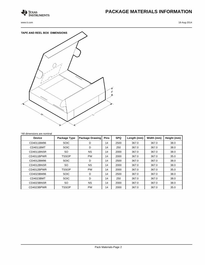
*All dimensions are nominal
Device Package Type Package Drawing Pins SPQ Length (mm) Width (mm) Height (mm)
CD4011BM96 SOIC D 14 2500 367.0 367.0 38.0
CD4011BMT SOIC D 14 250 367.0 367.0 38.0
CD4011BNSR SO NS 14 2000 367.0 367.0 38.0
CD4011BPWR TSSOP PW 14 2000 367.0 367.0 35.0
CD4012BM96 SOIC D 14 2500 367.0 367.0 38.0
CD4012BNSR SO NS 14 2000 367.0 367.0 38.0
CD4012BPWR TSSOP PW 14 2000 367.0 367.0 35.0
CD4023BM96 SOIC D 14 2500 367.0 367.0 38.0
CD4023BMT SOIC D 14 250 367.0 367.0 38.0
CD4023BNSR SO NS 14 2000 367.0 367.0 38.0
CD4023BPWR TSSOP PW 14 2000 367.0 367.0 35.0
PACKAGE MATERIALS INFORMATION
www.ti.com 18-Aug-2014
Pack Materials-Page 2
www.ti.com
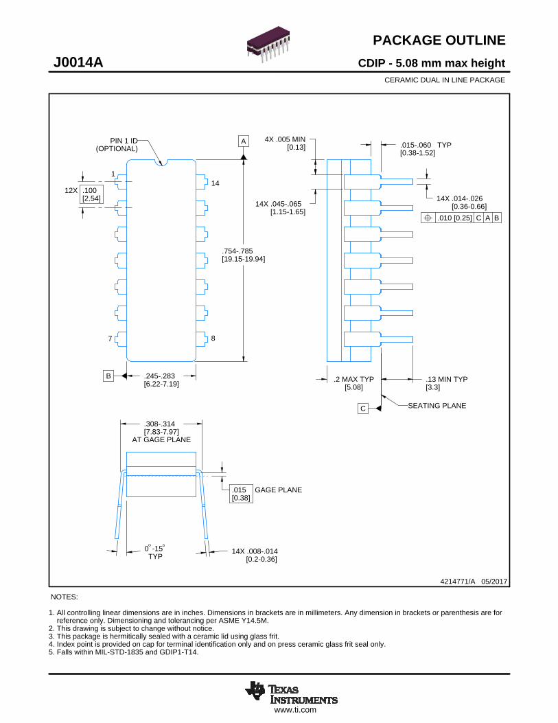
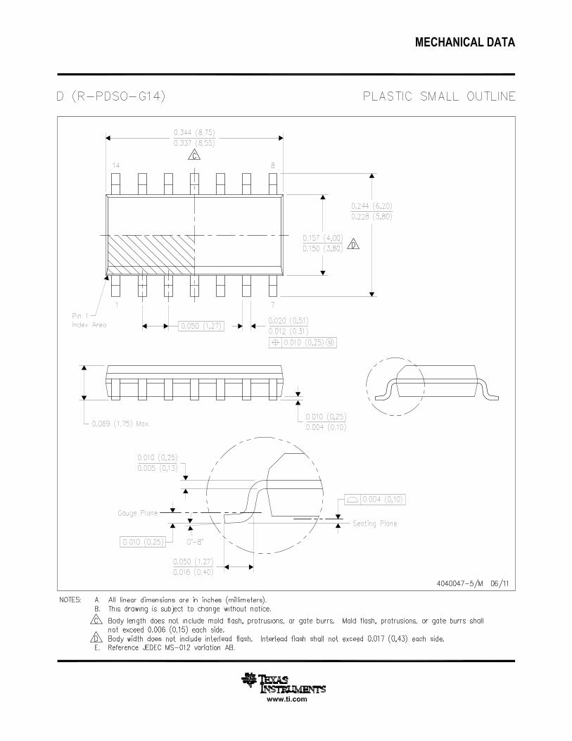
PACKAGE OUTLINE
C
14X .008-.014 [0.2-0.36]TYP
-150
AT GAGE PLANE
-.314.308-7.977.83[ ]
14X -.026.014-0.660.36[ ]14X -.065.045
-1.651.15[ ]
.2 MAX TYP[5.08]
.13 MIN TYP[3.3]
TYP-.060.015-1.520.38[ ]
4X .005 MIN[0.13]
12X .100[2.54]
.015 GAGE PLANE[0.38]
A
-.785.754-19.9419.15[ ]
B -.283.245-7.196.22[ ]
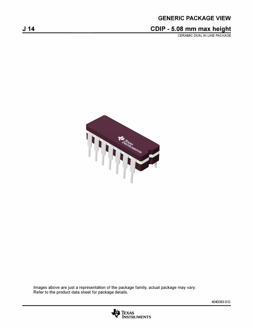
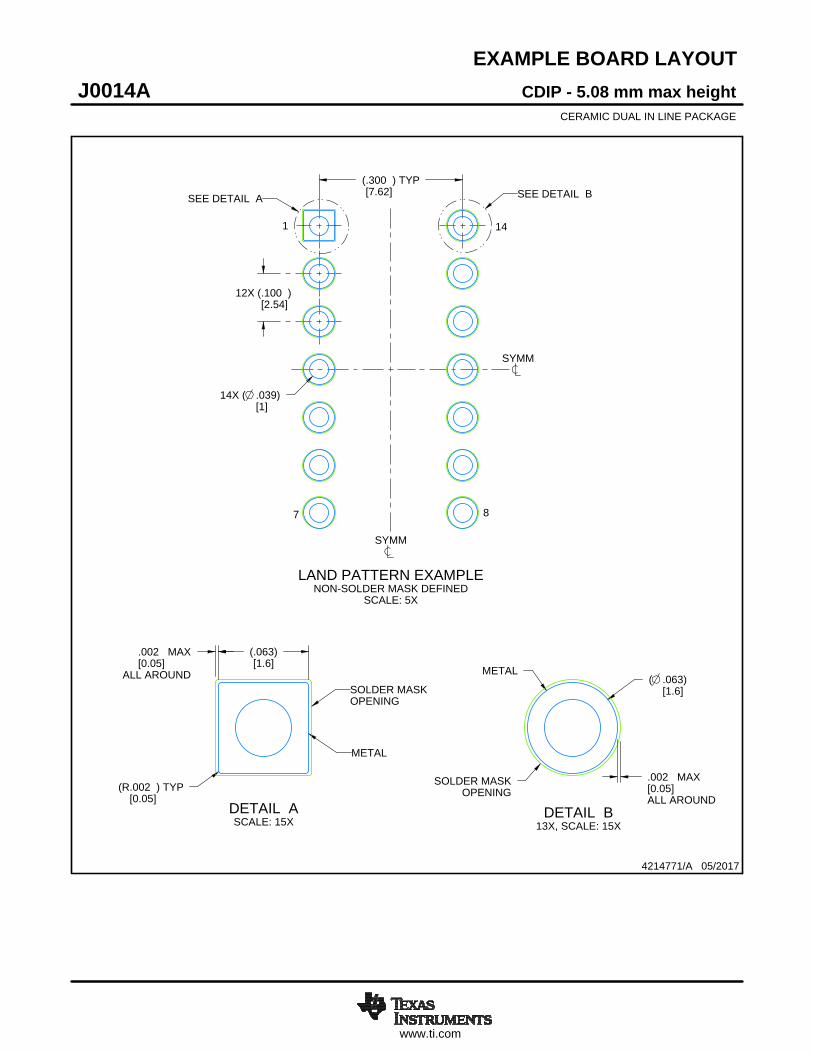
CDIP - 5.08 mm max heightJ0014ACERAMIC DUAL IN LINE PACKAGE
4214771/A 05/2017
NOTES: 1. All controlling linear dimensions are in inches. Dimensions in brackets are in millimeters. Any dimension in brackets or parenthesis are for reference only. Dimensioning and tolerancing per ASME Y14.5M.2. This drawing is subject to change without notice. 3. This package is hermitically sealed with a ceramic lid using glass frit.4. Index point is provided on cap for terminal identification only and on press ceramic glass frit seal only.5. Falls within MIL-STD-1835 and GDIP1-T14.
7 8
141
PIN 1 ID(OPTIONAL)
SCALE 0.900
SEATING PLANE
.010 [0.25] C A B
www.ti.com
EXAMPLE BOARD LAYOUT
ALL AROUND[0.05]
MAX.002
.002 MAX[0.05]ALL AROUND
SOLDER MASKOPENING
METAL
(.063)[1.6]
(R.002 ) TYP[0.05]
14X ( .039)[1]
( .063)[1.6]
12X (.100 )[2.54]
(.300 ) TYP[7.62]
CDIP - 5.08 mm max heightJ0014ACERAMIC DUAL IN LINE PACKAGE
4214771/A 05/2017
LAND PATTERN EXAMPLENON-SOLDER MASK DEFINED
SCALE: 5X
SEE DETAIL A SEE DETAIL B
SYMM
SYMM
1
7 8
14
DETAIL ASCALE: 15X
SOLDER MASKOPENING
METAL
DETAIL B13X, SCALE: 15X
IMPORTANT NOTICE
Texas Instruments Incorporated (TI) reserves the right to make corrections, enhancements, improvements and other changes to itssemiconductor products and services per JESD46, latest issue, and to discontinue any product or service per JESD48, latest issue. Buyersshould obtain the latest relevant information before placing orders and should verify that such information is current and complete.TI’s published terms of sale for semiconductor products (http://www.ti.com/sc/docs/stdterms.htm) apply to the sale of packaged integratedcircuit products that TI has qualified and released to market. Additional terms may apply to the use or sale of other types of TI products andservices.Reproduction of significant portions of TI information in TI data sheets is permissible only if reproduction is without alteration and isaccompanied by all associated warranties, conditions, limitations, and notices. TI is not responsible or liable for such reproduceddocumentation. Information of third parties may be subject to additional restrictions. Resale of TI products or services with statementsdifferent from or beyond the parameters stated by TI for that product or service voids all express and any implied warranties for theassociated TI product or service and is an unfair and deceptive business practice. TI is not responsible or liable for any such statements.Buyers and others who are developing systems that incorporate TI products (collectively, “Designers”) understand and agree that Designersremain responsible for using their independent analysis, evaluation and judgment in designing their applications and that Designers havefull and exclusive responsibility to assure the safety of Designers' applications and compliance of their applications (and of all TI productsused in or for Designers’ applications) with all applicable regulations, laws and other applicable requirements. Designer represents that, withrespect to their applications, Designer has all the necessary expertise to create and implement safeguards that (1) anticipate dangerousconsequences of failures, (2) monitor failures and their consequences, and (3) lessen the likelihood of failures that might cause harm andtake appropriate actions. Designer agrees that prior to using or distributing any applications that include TI products, Designer willthoroughly test such applications and the functionality of such TI products as used in such applications.TI’s provision of technical, application or other design advice, quality characterization, reliability data or other services or information,including, but not limited to, reference designs and materials relating to evaluation modules, (collectively, “TI Resources”) are intended toassist designers who are developing applications that incorporate TI products; by downloading, accessing or using TI Resources in anyway, Designer (individually or, if Designer is acting on behalf of a company, Designer’s company) agrees to use any particular TI Resourcesolely for this purpose and subject to the terms of this Notice.TI’s provision of TI Resources does not expand or otherwise alter TI’s applicable published warranties or warranty disclaimers for TIproducts, and no additional obligations or liabilities arise from TI providing such TI Resources. TI reserves the right to make corrections,enhancements, improvements and other changes to its TI Resources. TI has not conducted any testing other than that specificallydescribed in the published documentation for a particular TI Resource.Designer is authorized to use, copy and modify any individual TI Resource only in connection with the development of applications thatinclude the TI product(s) identified in such TI Resource. NO OTHER LICENSE, EXPRESS OR IMPLIED, BY ESTOPPEL OR OTHERWISETO ANY OTHER TI INTELLECTUAL PROPERTY RIGHT, AND NO LICENSE TO ANY TECHNOLOGY OR INTELLECTUAL PROPERTYRIGHT OF TI OR ANY THIRD PARTY IS GRANTED HEREIN, including but not limited to any patent right, copyright, mask work right, orother intellectual property right relating to any combination, machine, or process in which TI products or services are used. Informationregarding or referencing third-party products or services does not constitute a license to use such products or services, or a warranty orendorsement thereof. Use of TI Resources may require a license from a third party under the patents or other intellectual property of thethird party, or a license from TI under the patents or other intellectual property of TI.TI RESOURCES ARE PROVIDED “AS IS” AND WITH ALL FAULTS. TI DISCLAIMS ALL OTHER WARRANTIES ORREPRESENTATIONS, EXPRESS OR IMPLIED, REGARDING RESOURCES OR USE THEREOF, INCLUDING BUT NOT LIMITED TOACCURACY OR COMPLETENESS, TITLE, ANY EPIDEMIC FAILURE WARRANTY AND ANY IMPLIED WARRANTIES OFMERCHANTABILITY, FITNESS FOR A PARTICULAR PURPOSE, AND NON-INFRINGEMENT OF ANY THIRD PARTY INTELLECTUALPROPERTY RIGHTS. TI SHALL NOT BE LIABLE FOR AND SHALL NOT DEFEND OR INDEMNIFY DESIGNER AGAINST ANY CLAIM,INCLUDING BUT NOT LIMITED TO ANY INFRINGEMENT CLAIM THAT RELATES TO OR IS BASED ON ANY COMBINATION OFPRODUCTS EVEN IF DESCRIBED IN TI RESOURCES OR OTHERWISE. IN NO EVENT SHALL TI BE LIABLE FOR ANY ACTUAL,DIRECT, SPECIAL, COLLATERAL, INDIRECT, PUNITIVE, INCIDENTAL, CONSEQUENTIAL OR EXEMPLARY DAMAGES INCONNECTION WITH OR ARISING OUT OF TI RESOURCES OR USE THEREOF, AND REGARDLESS OF WHETHER TI HAS BEENADVISED OF THE POSSIBILITY OF SUCH DAMAGES.Unless TI has explicitly designated an individual product as meeting the requirements of a particular industry standard (e.g., ISO/TS 16949and ISO 26262), TI is not responsible for any failure to meet such industry standard requirements.Where TI specifically promotes products as facilitating functional safety or as compliant with industry functional safety standards, suchproducts are intended to help enable customers to design and create their own applications that meet applicable functional safety standardsand requirements. Using products in an application does not by itself establish any safety features in the application. Designers mustensure compliance with safety-related requirements and standards applicable to their applications. Designer may not use any TI products inlife-critical medical equipment unless authorized officers of the parties have executed a special contract specifically governing such use.Life-critical medical equipment is medical equipment where failure of such equipment would cause serious bodily injury or death (e.g., lifesupport, pacemakers, defibrillators, heart pumps, neurostimulators, and implantables). Such equipment includes, without limitation, allmedical devices identified by the U.S. Food and Drug Administration as Class III devices and equivalent classifications outside the U.S.TI may expressly designate certain products as completing a particular qualification (e.g., Q100, Military Grade, or Enhanced Product).Designers agree that it has the necessary expertise to select the product with the appropriate qualification designation for their applicationsand that proper product selection is at Designers’ own risk. Designers are solely responsible for compliance with all legal and regulatoryrequirements in connection with such selection.Designer will fully indemnify TI and its representatives against any damages, costs, losses, and/or liabilities arising out of Designer’s non-compliance with the terms and provisions of this Notice.
Mailing Address: Texas Instruments, Post Office Box 655303, Dallas, Texas 75265Copyright © 2017, Texas Instruments Incorporated