Embed Size (px)
Citation preview

Data Path Implementation for a Spatially Programmable Architecture Customized
for Image Processing Applications
by
Saktiswarup Satapathy
A Thesis Presented in Partial Fulfillment
of the Requirements for the Degree
Master of Science
Approved June 2016 by the
Graduate Supervisory Committee:
John Brunhaver, Chair
Lawrence T. Clark
Fengbo Ren
ARIZONA STATE UNIVERSITY
August 2016

i
ABSTRACT
The last decade has witnessed a paradigm shift in computing platforms, from
laptops and servers to mobile devices like smartphones and tablets. These devices host an
immense variety of applications many of which are computationally expensive and thus
are power hungry. As most of these mobile platforms are powered by batteries, energy
efficiency has become one of the most critical aspects of such devices. Thus, the energy
cost of the fundamental arithmetic operations executed in these applications has to be
reduced. As voltage scaling has effectively ended, the energy efficiency of integrated
circuits has ceased to improve within successive generations of transistors. This resulted in
widespread use of Application Specific Integrated Circuits (ASIC), which provide
incredible energy efficiency. However, these are not flexible and have high non-recurring
engineering (NRE) cost. Alternatively, Field Programmable Gate Arrays (FPGA) offer
flexibility to implement any application, but at the cost of higher area and energy compared
to ASIC.
In this work, a spatially programmable architecture customized for image
processing applications is proposed. The intent is to bridge the efficiency gap between
ASICs and FPGAs, by offering FPGA-like flexibility and ASIC-like energy efficiency.
This architecture minimizes the energy overheads in FPGAs, which result from the use of
fine-grained programming style and global interconnect. It is flexible compared to an ASIC
and can accommodate multiple applications.
The main contribution of the thesis is the feasibility analysis of the data path of this
architecture, customized for image processing applications. The data path is implemented
at the register transfer level (RTL), and the synthesis results are obtained in 45nm

ii
technology cell library from a leading foundry. The results of image-processing
applications demonstrate that this architecture is within a factor of 10x of the energy and
area efficiency of ASIC implementations.

iii
ACKNOWLEDGMENTS
I would like to thank Dr. Brunhaver for offering me the research opportunity and
guiding me throughout the master’s program. I would also like to thank my committee
members Dr. Clark and Dr. Ren for their time and support. I must also thank my research
colleagues Curtis and Ron for the technical discussions and support.
I would like to express my gratitude towards my family for their constant support
and encouragement.
iv
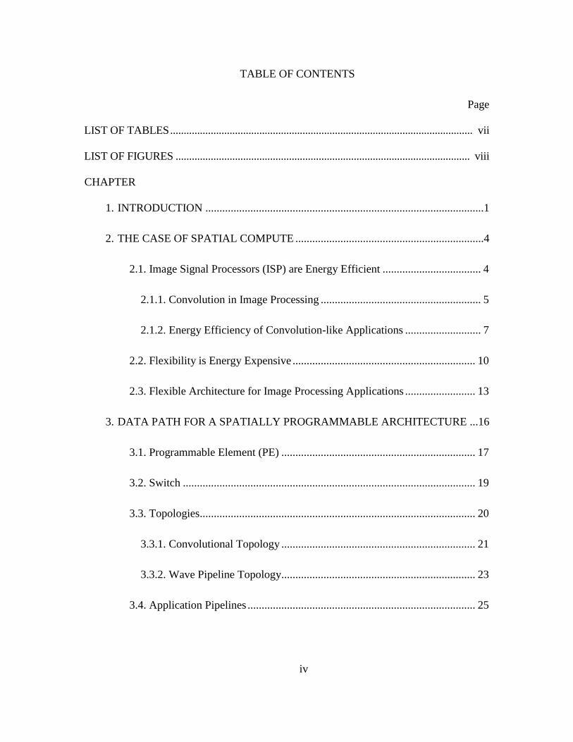
TABLE OF CONTENTS
Page
LIST OF TABLES ................................................................................................................ vii
LIST OF FIGURES ............................................................................................................. viii
CHAPTER
1. INTRODUCTION ...................................................................................................1
2. THE CASE OF SPATIAL COMPUTE ...................................................................4
2.1. Image Signal Processors (ISP) are Energy Efficient ................................... 4
2.1.1. Convolution in Image Processing ......................................................... 5
2.1.2. Energy Efficiency of Convolution-like Applications ........................... 7
2.2. Flexibility is Energy Expensive ................................................................. 10
2.3. Flexible Architecture for Image Processing Applications ......................... 13
3. DATA PATH FOR A SPATIALLY PROGRAMMABLE ARCHITECTURE ...16
3.1. Programmable Element (PE) ..................................................................... 17
3.2. Switch ........................................................................................................ 19
3.3. Topologies.................................................................................................. 20
3.3.1. Convolutional Topology ..................................................................... 21
3.3.2. Wave Pipeline Topology..................................................................... 23
3.4. Application Pipelines ................................................................................. 25

v
CHAPTER Page
4. METHODOLOGY .................................................................................................26
4.1. Generation of the Data Path Hardware ...................................................... 26
4.1.1. Introduction to Genesis2 ..................................................................... 26
4.1.2. Parameterization for the Data Path Implementation ........................... 28
4.2. Compiling Applications on the Architecture ............................................. 31
4.3. Implementation Methodology .................................................................... 32
4.4. FPGA Methodology ................................................................................... 34
5. RESULTS…….. ....................................................................................................35
5.1. Results for Convolutional Topology .......................................................... 36
5.1.1. Cost for Different Precisions of Operation ......................................... 36
5.1.2. Cost of the Local Interconnect ............................................................ 38
5.1.3. Results for Obtaining the Clock Frequency ........................................ 40
5.2. Result for Wave Pipeline Topology ........................................................... 41
5.2.1. Experiments to Find the Cost of Flexibility ........................................ 41
5.2.2. Application Results ............................................................................. 43
5.3. Conclusions from the Result ...................................................................... 46
6. CONCLUSION AND FUTURE WORK ..............................................................48
6.1. Thesis Summary and Conclusion............................................................... 48
6.2. Scope of Future Work ................................................................................ 48

vi
Page
REFERENCES………………………………………………………………......50

vii
LIST OF TABLES
Table Page
2-1 Energy Costs of Different Operations.. ........................................................................ 8
3-1 Parameters Used in PE ............................................................................................... 18
3-2 Parameters Used in Switch ......................................................................................... 20
3-3 Parameterization of Convolution Topology ............................................................... 23
3-4 Parameterization of Wave Pipeline Topology ............................................................ 25

viii
LIST OF FIGURES
Figure Page
2.1 Convolution of an 8x8 Image with 3x3 Window of Operation .................................... 5
2.2 Kernel Operations Performed for a 3x3 Convolution ................................................... 5
2.3 Stencil Kernel Architecture for Convolution ................................................................ 6
2.4 Cascading Kernels in Image Processing Applications .................................................. 7
2.5 Trade-off Between Flexibility and Efficiency ............................................................ 10
2.6 Architectural Abstraction of a Flexible Application Pipeline..................................... 13
2.7 Inner Loop of Convolution in a High-level Language................................................ 14
3.1 Block Diagram of Programmable Element (PE) ........................................................ 17
3.2 Block Diagram of a 3x2 Switch .................................................................................. 19
3.3 Detailed Block Diagram of 2x2 Convolution Topology............................................. 22
3.4 DAG Representation for a Stage of Canny Edge Detection ....................................... 24
3.5 Abstract Block Diagram of Wave Pipeline Topology ................................................ 24
3.6 Construction of Application Pipeline.......................................................................... 25
4.1 Compilation of Genesis2 Code ................................................................................... 27
4.2 Parameterization in Genesis2 ...................................................................................... 27
4.3 Procedural Generation of Data Path Hardware ........................................................... 28
4.4 Pseudo Code to Create the Data Structures of PEs and Switches ............................... 29
4.5 Pseudo Code to Instantiate PEs and Switches ............................................................ 30
4.6 Pseudo Code for the Interconnection of PEs, Switches, and System Interface .......... 30
4.7 External Configuration of Parameters for Convolution .............................................. 30
4.8 Flow for Compilation of Applications on the Architecture ........................................ 31
ix
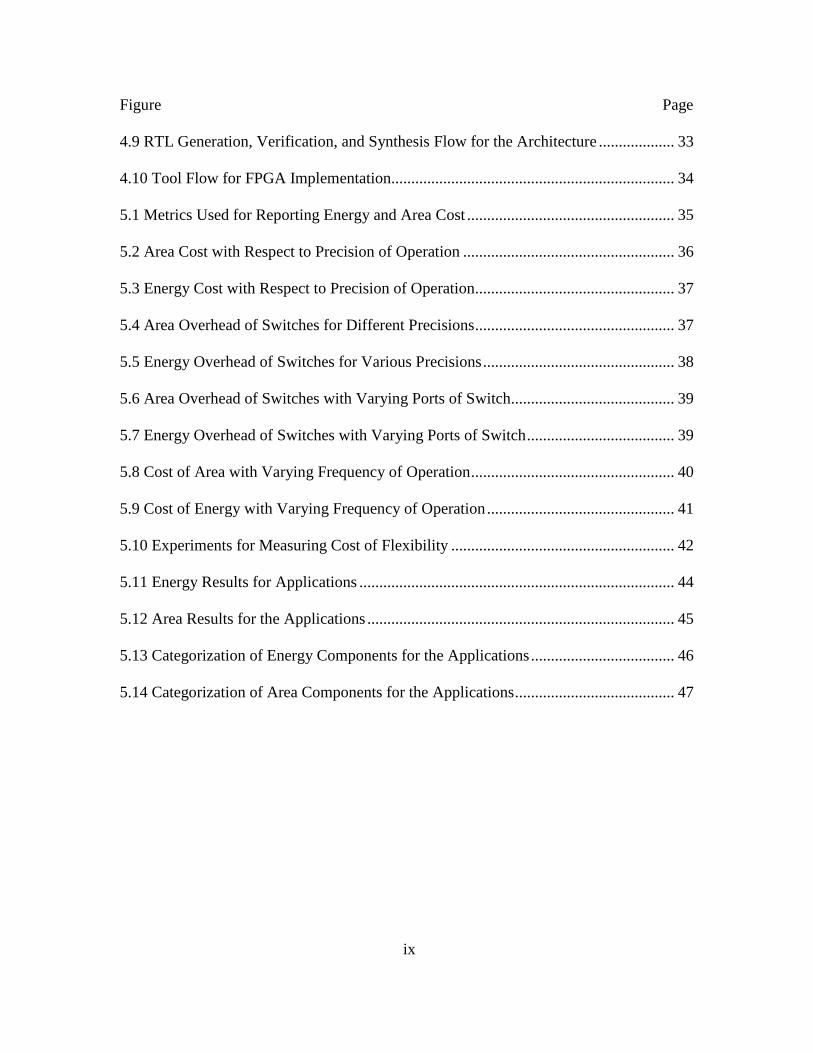
Figure Page
4.9 RTL Generation, Verification, and Synthesis Flow for the Architecture ................... 33
4.10 Tool Flow for FPGA Implementation....................................................................... 34
5.1 Metrics Used for Reporting Energy and Area Cost .................................................... 35
5.2 Area Cost with Respect to Precision of Operation ..................................................... 36
5.3 Energy Cost with Respect to Precision of Operation .................................................. 37
5.4 Area Overhead of Switches for Different Precisions .................................................. 37
5.5 Energy Overhead of Switches for Various Precisions ................................................ 38
5.6 Area Overhead of Switches with Varying Ports of Switch ......................................... 39
5.7 Energy Overhead of Switches with Varying Ports of Switch ..................................... 39
5.8 Cost of Area with Varying Frequency of Operation ................................................... 40
5.9 Cost of Energy with Varying Frequency of Operation ............................................... 41
5.10 Experiments for Measuring Cost of Flexibility ........................................................ 42
5.11 Energy Results for Applications ............................................................................... 44
5.12 Area Results for the Applications ............................................................................. 45
5.13 Categorization of Energy Components for the Applications .................................... 46
5.14 Categorization of Area Components for the Applications ........................................ 47

1
CHAPTER 1. INTRODUCTION
The battery life of our ubiquitous mobile computing devices like mobile phones,
tablets, cameras, smart watches, and smart health monitoring systems is determined by the
energy efficiency of their computations. For applications that must process an abundance
of data like image processing, computer vision, etc., this often requires that the energy cost
of an arithmetic operation be very small. Since most of these mobile devices operate
independently, these need to be very high performance to execute the algorithms in real
time. Since battery life depends on energy consumption, this calls for energy efficient
integrated circuit designs. Further, given power constraints, due to thermal limits of mobile
devices, energy efficiency determines performance (Power = Performance * Energy)
[Mark14].
Traditionally, the energy cost of arithmetic operation scaled cubically with feature
size. Unfortunately, voltage scaling has effectively ended [Denn99]. Moreover, traditional
technology scaling has slowed down [ITRS10, Cunn14], which is officially confirmed by
Intel as they announced the extension of the life cycle for each process [Dent16]. Hence,
we need to do something other than waiting for better transistors.
Application Specific Integrated Circuits (ASIC) (fixed function hardware) are
incredibly energy efficient and outclass the general purpose CPU or GPU by three orders
of magnitude in terms of energy efficiency and performance [Chen14, Mark12]. ASICs
achieve that efficiency by exploiting the structure of the algorithms [Mark12] and reducing
the flexibility [Qadeer13]. Thus, ASICs are often employed in mobile System on Chips
(SoC) for critical applications, which include image processing, computer vision, and video
rendering applications.
2
Unfortunately, fixing the function of hardware represents an incredible opportunity
cost. The resources allocated to ASIC (e.g. design, verification, silicon area, etc.) cannot
be used for other applications. This often means that an algorithm is fixed well in advance
of tape-out eliminating future opportunities for optimization.
Alternatively, Field Programmable Gate Arrays (FPGA) are more flexible
architectures. These can be used to implement any application that has an ASIC
implementation. FPGA allows reconfiguration of the hardware after manufacturing, to
accommodate newer applications. Additionally, FPGAs will generally have a lower unit
cost for small volumes.
However, FPGAs lack efficiency compared to ASICs. The flexibility of FPGAs
comes at the expense of higher energy consumption, increased area usage, and slower clock
frequency of operation. FPGAs are ~35X larger in silicon area, ~4X slower in performance
and ~25X to ~50X energy expensive than ASICs for the same technology node [Kuon07].
A more efficient architecture would be something that offers the flexibility of
FPGA’s and energy efficiency of ASIC’s. In this thesis, a spatially programmable
architecture (SPA), customized for image processing applications, is proposed. It aims at
bridging the gap between ASICs and FPGAs by offering flexibility as an FPGA while
remaining energy/area efficient with respect to ASICs. Compared to FPGA, the proposed
architecture reduces overheads by employing local interconnects instead of global
interconnects and follows a coarse-grained approach both in terms of functionality and
precision of operation rather than fine-grained programmability. Additionally, the
architecture can accommodate multiple applications, thus allowing flexibility compared to
an ASIC.

3
The main contribution of this work is to demonstrate the feasibility of the data path
for this architecture in terms of its functionality and energy efficiency. This is achieved by
implementing the data path in Register Transfer Level (RTL) and performing topologically
driven synthesis to obtain accurate energy/area results.

4
CHAPTER 2. THE CASE OF SPATIAL COMPUTE
Fixed function hardware for image signal processing is incredibly energy efficient
(Sec 2.1). Image processing applications greatly resemble the working of convolution
operation (Sec 2.1.1). Applications in image processing domain have the inherent
properties of energy efficient computations that allow building efficient fixed function
hardware for these (Sec 2.1.2). However, Image Signal Processors (ISP) are not flexible
and only suitable for a specific application. Alternatively, programmable architectures
sacrifice energy/area efficiency for flexibility (Sec 2.2). In this work, a spatially
programmable architecture is proposed for image processing applications, which is flexible
while being energy efficient as fixed function hardware (Sec 2.3).
2.1. Image Signal Processors (ISP) are Energy Efficient
Image Signal Processors are employed for the acceleration of image processing
algorithms in camera and mobile phone SoCs. ISPs perform various noise reduction/image
enhancement algorithms on the raw sensor data and produce a colored image [Adams10].
ISPs constitute pipeline of image kernels, where each stage of the pipeline represents a
specific kernel of an image processing application. The output pixel in a kernel is computed
based on a limited region of input image pixels.
The kernels in ISPs mirror the function of a convolution kernel [Brun15].
Convolution is a commonly used algorithm used for performing various filter effects on an
image. The algorithms in image processing have similar working like that of a two-
dimensional convolution operation of an image.

5
2.1.1. Convolution in Image Processing
Figure 2.1 Convolution of an 8x8 image with 3x3 window of operation
Figure 2.2 Kernel operations performed for a 3x3 convolution
In convolution, the output pixel is determined based on a small rectangular window
of the input image pixels and few constant coefficients. The output pixels are calculated in
row-major order. Convolution works in a sliding window fashion, where the working
window traverses the entire input image in row-major order to produce the pixel values for
the output image. This sliding window is referred to as stencil [Kung79, Kung88, Coll60].
Figure 2.1and Figure 2.2 show the working of two-dimensional convolution for an 8x8
resolution of the image with a window size of 3x3. For this specific example, the 3x3
sliding window starts at the upper left corner of the image and slides right, through all the

6
columns, until it reaches the end of a row. It again starts at the leftmost corner of the next
row.
Figure 2.3 Stencil kernel architecture for Convolution
The hardware implementation of convolution kernel contains a line buffer, a stencil
register, and a window function as represented in Brunhaver’s work [Brun15]. This is
shown in Figure 2.3. The stencil register is a shift register and supplies the pixel values in
the sliding window to the execution unit of the architecture. The data path of this
architecture is shown as the window function (Figure 2.3). It executes arithmetic
computations based on the input data from stencil register and calculates the output pixel.
The rows of pixel values, which are re-used between successive row traversals, are stored
in local memory (SRAM arrays). These buffers are called as line buffers [Reutz86,
Kamp90, Zehner86]. The line buffer provides a column of pixel values to the stencil
register for each overlapping window of the input image.
Image signal processing applications are organized into the pipeline of kernels. This
is shown in Figure 2.4. Each of these functional kernels works the same way as a
convolution kernel. These convolution-like applications can be implemented by
interconnecting the hardware components that are used for a single kernel [Brun15].

7
F(x) F(y)
Figure 2.4 Cascading kernels in image processing applications
2.1.2. Energy efficiency of convolution-like applications
An energy efficient application spends little energy for many arithmetic operations.
As the cost of different operations varies (Table 2-1), energy efficient applications favor
less expensive operations over more expensive operations. For energy efficient
computation, the energy overheads relative to the cost of an arithmetic operation need to
be reduced. The sources of these energy overheads are global memory (DRAM) access,
local memory (SRAM) access, instructions and high precision operations [Brun15]. From
Table 2-1, it is evident that the global memory access is an incredibly costly operation,
which is three orders of magnitude energy expensive than the fundamental arithmetic work
performed in an application.
To amortize the DRAM energy overheads, we are interested in applications with a
high compute-to-bandwidth ratio [Brun15, Sites96, Nowa96]. In Convolution-like
applications, pixel values for the input image are fetched from global memory and fed into
the deeply pipelined kernels that perform a large number of computations. Pixel values for
an image at any stage of the pipeline is computed from a finite window of pixels from the
image in the prior stage. Intermediate values between each stage are stored in line buffers.
The deeply pipelined kernels execute thousands of arithmetic operations per pixel access
from global memory, which amortizes the overheads of DRAM read operations.

8
Operation Energy Order
8b add 0.05 pJ 1
8b mult 0.20 pJ 4
64b FMA 8.0 pJ 160
8b Reg File Ld 0.38 pJ 8
8b SRAM Ld 2.5 pJ 50
8b DRAM Ld 320 pJ 6400
RISC Instr. 50 pJ 1000
SIMD Instr. 250 pJ 5000
Table 2-1 Energy costs of different operations. The 8-bit addition, 8-bit multiplication and
64-bit floating point multiply and accumulate results are obtained from the
synthesis of these designs using 45nm cell library [Brun15].The memory
operation costs are obtained from Cacti [Mura09]. The SIMD and RISC costs
are obtained based on Tensilica cores [hameed10, Qadeer13].
We are interested in applications with a minimal working set [Ragan12] that can fit
into the on-chip memory to avoid redundant global memory accesses [Brun15]. The
working set of any application refers to the DRAM reads that are re-used over multiple
operations. In convolution-like applications, the lines of pixel values that are re-used
between successive rows constitute the total working set of the application. Hence, this
working set is finite, and it is stored in line buffer so that pixel values need not be re-read
from DRAM memory.
SRAM reads that are instantly re-used should be stored in local registers to
minimize accesses to local memory [Brun15]. Applications that allow significant reuse of
data are said to have high locality (temporal and spatial locality) [Lee14]. The temporal
locality refers to the reuse of data in the near future, and spatial locality is the use of

9
neighboring locations of a referenced data. In convolution-like applications, the column of
pixel values that are immediately re-used in overlapping sliding window operations, are
stored in local stencil registers. For a 3x3-stencil operation, one column of three-pixel
values is read from the line buffer and stored in stencil register, which is re-used for three
consecutive sliding window operations. This avoids redundant access to the line buffer.
To amortize the instruction overhead costs, we are interested in applications that
perform a large number of computations per instruction rather than executing a single
instruction for a single operation [Brun15, Hameed10]. This overhead is due to the energy
costs of different operations performed in a pipelined CPU that constitute instruction
fetching, decoding, branch prediction, etc. It is the cost of flexibility provided by general-
purpose processors [Hameed10, Venkat10]. The operations performed in the kernels of
convolution-like applications are functional in nature (e.g. multiply and accumulate, the
sum of absolute difference, etc.). Hence, these operations can be unrolled in space and
mapped to distinct execution units [Brun15]. Thus, we can perform multiple operations
using a single instruction and minimize the instruction overhead.
Finally, we are interested in applications that employ inexpensive lower precision
operations to reduce the energy cost of arithmetic operations [Brun15]. Image-processing
applications work on pixel values that are generally represented by low precision 8 or 12-
bit integers. This allows minimum overheads for arithmetic operations.
Thus, image-processing applications show the properties of energy efficient
computation by having: “significant immediate re-use, finite and small working set,
functional in execution such that the computation can be unrolled in space and low

10
precision in operation” [Brun15]. Hence, fixed function ISPs build for image processing
applications are incredibly energy efficient.
While ISPs are extremely energy efficient, these are not flexible. We have to build
custom ASICs for every application. This presents a huge opportunity cost, thus makes this
hardware undesirable. A desirable solution would be to have a programmable architecture
that can cater to multiple applications while being energy efficient.
2.2. Flexibility is Energy Expensive
Figure 2.5 Trade-off between flexibility and efficiency
Increased programmability in an architecture comes at the cost of energy and area
efficiency. The general purpose CPUs and GPUs are incredibly flexible and have robust
application development tools to cater many applications across various domains.
However, these are three orders of magnitude energy and area expensive compared to an
ASIC implementation for any application [Chen14, Mark12]. Figure 2.5 shows the energy

11
per operation and area per performance for various architectures. These values are gathered
based on the work presented at ISSCC and JSSC [Mark12]. The FPGA value is based on
Kuon’s work [Kuon07].
Digital Signal Processors (DSP) are some of the architectures, which fall between
CPU/GPU and ASIC regarding energy and area efficiency while providing flexibility.
DSPs are specialized architectures used for signal processing applications, and its
instructions are optimized for the operational needs of this domain of applications. Still,
DSPs are at least an order of magnitude more energy expensive compared to ASICs
[Mark12].
Alternatively, Field Programmable Gate Arrays (FPGA) are the closest to ASICs
in terms of efficiency while offering immense flexibility to implement any application.
FPGAs are load-time programmable architectures that can be re-configured after
manufacturing to accommodate new applications. On the other hand, ASICs has to undergo
full design and production cycle for any changes in the application. This led to FPGA being
widely used for prototyping any application and its throughput comes close to an ASIC
[Yuan15].
However, the flexibility of FPGAs come at the cost of higher energy consumption
and area usage compared to ASICs. These inefficiencies can be attributed to certain
overheads in FPGAs. First, there are overheads due to a vast number of look-up-tables
(LUT) employed in FPGAs for offering fine-grained programming at the bit level
[Comp02, Marq00]. Second, these LUTs are connected through 2D based interconnects
that form global connections. The global interconnect network account for the bulk of

12
FPGA’s area, contribute to significant power consumption, and slower speed [Yuan15,
Kuon07, Bols06, Merr13].
Additionally, FPGAs have excessive compilation times and are slow to re-program.
The flexibility of FPGAs is derived from the fine-grained architecture style by employing
bit level granular LUTs and global on-chip network. This type of generic structures creates
a vast number of alternative options for the physical implementation algorithms [Para13].
Hence, the implementation step has excessive run times for FPGA fabric. Moreover,
FPGAs are load-time programmable using bit streams. For reconfiguring the hardware, the
new bit streams must be generated and loaded into its memory, which is a time-consuming
process.
A more desirable architecture would be something that closes the efficiency gap
between ASICs and FPGAs while being easy to program. Naturally, many programmable
architectures are targeted at bridging this gap. These are Systolic Arrays [Pedram12,
Kung79], Coarse-Grained Reconfigurable Arrays (CGRA) [Govind12, Govind11,
Qadeer13, Para13], PipeRench [Copen99], RAW [Taylor02] etc.
This work shows the implementation of image-processing applications on a flexible
architecture whose energy efficiency is comparable to an ASIC. This is achieved by
optimizing the FPGAs and reducing their energy overheads. First, rather than having a
fine-grained architecture style of FPGA, we follow a coarse-grained approach in terms of
functionality and precision of operation. This reduces the overheads because of the LUTs.
Second, we employ local interconnect instead of global interconnect. This reduces the
routing overheads compared to FPGAs.

13
2.3. Flexible architecture for image processing applications
The stencil kernel abstraction (Figure 2.3) can be used for building hardware for
image processing applications. Different kernels are cascaded to form a pipeline for any
Convolution-like application as shown in Figure 2.6. The pixel output from each stage is
fed to the line buffer of the next stage, thus forming a producer-consumer relationship
between stages. For creating a flexible architecture, we need to have flexible line buffers,
flexible stencil registers, and flexible window function hardware.
Line Buffer1
Window Function1
Stencil Register1
Line Buffer2
Window Function2
Stencil Register2
Line Buffer3
Window Function3
Stencil Register3
Figure 2.6 Architectural abstraction of a flexible application pipeline

14
In this work, the focus is to design a flexible data path (window function) for this
abstraction that can support various kernel executions across many applications. The
window function performs computations on the stream of data, furnished by the stencil
register and calculates the output pixel value. The output pixel calculation is completely
functional that comprises of arithmetic functions like multiplication, subtraction, etc.
The window function is implemented as an optimization of FPGA fabric by
employing coarse-grained programming and limited local interconnect. Instead of using
fine-grained LUTs, we employ coarser functional units that execute operations at the word-
length precision (8bit, 16bit, etc.) instead of 1-bit precision. This implementation utilizes
the spatial programming model of FPGAs. These functional units are programmed in a
spatial manner to perform the computations.
A spatially programmable architecture distributes computations across a large
number of computing resources whose operation is fixed in time. These resources execute
the same function for the entire duration of any program. Whereas architectures that are
programmed in time (e.g. pipelined MIPS), employ a small number of resources that are
time multiplexed to execute the operations.
Figure 2.7 Inner loop of convolution in a high-level language

15
The proposed spatial programmable architecture (SPA) is suitable for
implementing programs having inner loops of operations. These programs repeatedly
execute a set of operations on a stream [kapa03, Thies02, Suger09] of input data. The inner
loop of operations is mapped to distinct compute resources in the fabric by means of spatial
programming. Figure 2.7 shows the inner loop of convolution operation. The inner loop of
this convolution program is unrolled in space so that individual operations in the loop (e.g.
multiply, sum) are mapped to distinct compute resources (Figure 3.3). Convolution-like
applications that have multiple inner loops can be implemented by interconnecting
different kernels (Figure 2.6). Each of the inner loops operates on the streams of input pixel
values from the previous stage.

16
CHAPTER 3. DATA PATH FOR A SPATIALLY PROGRAMMABLE
ARCHITECTURE
The data path of ASIC comprises fixed arithmetic units that execute operations and
has fixed connections between those units to facilitate the data flow. We can replace each
of these arithmetic units with a more flexible unit that supports multiple operations and
allows an operation to be selected at runtime. This flexible unit, which is reconfigurable at
runtime, is called a programmable element (PE). Again, if we substitute the wires between
the execution units with switches, then we can change the order of operations. Hence, the
abstract representation of a flexible data path would be the arbitrary interconnection of PEs
and Switches.
Different topologies for this data path abstraction are procedurally generated from
hardware templates with the help of chip generator [Shac10], Genesis2 [Shac15]. This
requires the translation of the design specification to Genesis2 parameters for the hardware
templates. The chip generator performs a rule-based elaboration to create a specific
instance of the design based on the parameters (Sec 4.1.1, Sec 4.1.2).
Domain-specific languages (DSL) like Darkroom provide the necessary structure to
map the image processing algorithms to a spatially programmable architecture [Hega14].
A compiler is built for the proposed spatial architecture that translates the intermediate
representations of the Darkroom code to a directed acyclic graph (DAG) of functions for
the kernels of an application and generates the machine code for running the applications
on the architecture [Mack16] (Sec 4.2).

17
`
Q
QSET
CLR
D
Q
QSET
CLR
D
Q
QSET
CLR
D
Q
QSET
CLR
D
Q
QSET
CLR
D
Q
QSET
CLR
D
Q
QSET
CLR
D
F(z)=x*y
F(z)=|x-y|
F(z)=x>y
F(z)=x<y
Q
QSET
CLR
D
Q
QSET
CLR
D
Q
QSET
CLR
D
Fab_to_Pe_SrIn
Fab_to_Pe[0]
Fab_to_Pe[1]
Fab_to_Pe_ScIn
Sel_Sr_Port
Sel_Sc_Port
Sel_FuncPe_to_Fab_valid[0]
Pe_to_Fab[1]
Pe_to_Fab[0]
Pe_to_Fab_SrOut
Valid_0
Valid_1
Valid_2
Local Reg Mux
Data Gate Data Mux
Config Reg
ShiftOut
ShiftReg
Figure 3.1 Block diagram of programmable element (PE)
3.1. Programmable Element (PE)
The programmable element is the execution unit of the fabric that is configured
during runtime to execute the same operation repeatedly for a given application. The block
diagram of PE is shown in Figure 3.1. The runtime programmability is achieved by
configuring the configuration register. The value in this register determines which of the
functions is executed during runtime. It can support arbitrary functions including
traditional programming language operators. At hardware generation time, the available
functions are determined by a parameter defining a list of functions.
PEs incorporate Local Reg Mux, Data Gate, Data Mux and some local
configuration registers. The local configuration registers are used to store the constant
coefficient values and shifted in pixel values for any kernel operation. The local reg mux

18
determines whether the values are taken from local configuration registers or from the
primary inputs. The purpose of the data gate is to reduce power by eliminating toggles at
the inputs of the functions, which are not selected during runtime. The data mux selects the
appropriate output based on the value in the instruction configuration register.
Parameter
Name
Legal
Values Description of Parameter
Functions mult,absDi
ff,gt,lt etc List of defined functions
PePipeDepth 1,2,3 etc Total number of flops at input and output side
DataWidth 4,8,16 bits
etc Precision of operation
Table 3-1 Parameters used in PE
Valid bits are associated with each of inputs and outputs of the PE. These are used
to implement push pipeline and pull pipeline. Additionally these help in simplifying the
reset. As we make the valid bits as zero for the inputs, this makes the outputs invalid
irrespective of reset.
Moreover, there are flip-flops at the inputs and outputs of the PE. The flip-flop for
the input shift register port allows incorporating a shift register connection inside the PE.
These flip-flops also help in storing the constant values for immediate operations.
Additionally, these flip-flops act as pipeline registers for timing.
Genesis2 parameters determine the exact implementation of the PE including its
number of inputs,outputs, the functions and the precision of operation. The list of functions
that are supported in PE is defined through a Genesis2 parameter. From this parameter, we
derive the number of input/output ports of the PEs (as required by the defined functions)
and the dimension of the config register, which selects the function at runtime. The number
19
of flip-flops at input/output side of the PE are determined by a parameter. Additionally, we
can implement any data precision for the operations with a Genesis2 parameter. This is
summarized in Table 3-1.
3.2. Switch
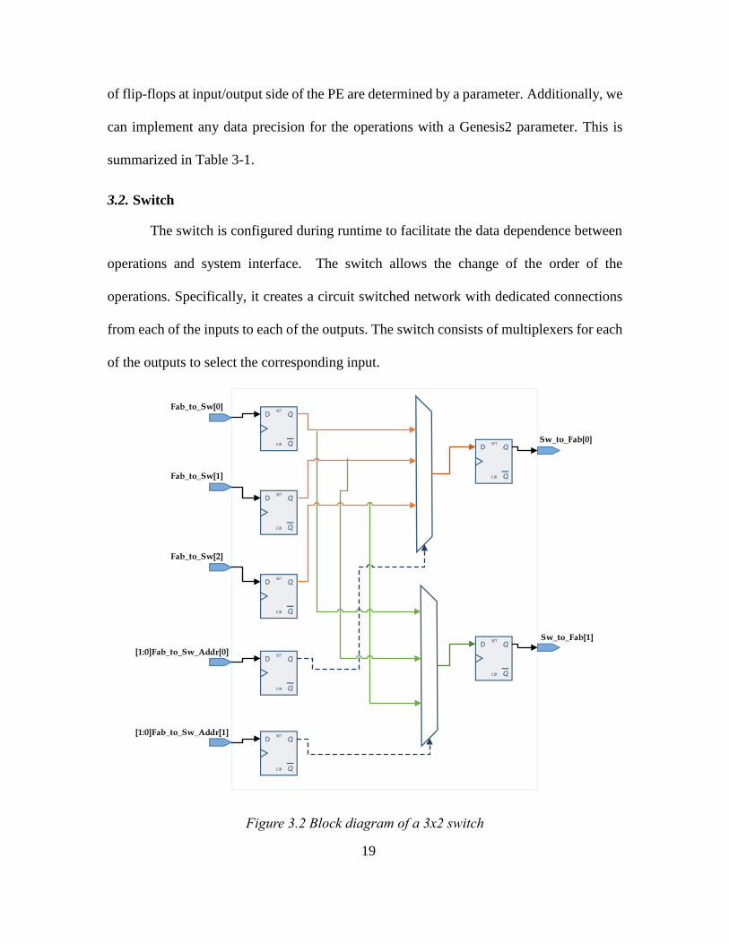
The switch is configured during runtime to facilitate the data dependence between
operations and system interface. The switch allows the change of the order of the
operations. Specifically, it creates a circuit switched network with dedicated connections
from each of the inputs to each of the outputs. The switch consists of multiplexers for each
of the outputs to select the corresponding input.
[1:0]Fab_to_Sw_Addr[0]
Sw_to_Fab[1]
Sw_to_Fab[0]
[1:0]Fab_to_Sw_Addr[1]
Q
QSET
CLR
D
Q
QSET
CLR
D
Q
QSET
CLR
D
Q
QSET
CLR
D
Q
QSET
CLR
D
Q
QSET
CLR
D
Fab_to_Sw[0]
Fab_to_Sw[1]
Fab_to_Sw[2]
Q
QSET
CLR
D
Figure 3.2 Block diagram of a 3x2 switch

20
The switch follows source based routing structure, where the input source of an
output is specified through configuration registers. The configuration register has the
unpacked dimension equal to the number of outputs and packed dimension equal to the
number of bits required for binary encoding of the primary inputs. The configuration
register’s dimensions are procedurally generated by the chip generator based on the
parameter values for the number of inputs and outputs of the switch. The parameters for
the switch are presented in Table 3-2.
Parameter
Name
Legal
Values Description of Parameter
DataWidth 4,8,16bit
etc Packed LHS dimensions of input and output signals
SwPipeDepth 1,2,3 etc Total number of flops at input and output side
InPortCount 1,2,3 etc Number of inputs of Switch
OutPortCount 1,2,3 etc Number outputs of the Switch
Table 3-2 Parameters used in Switch
The block diagram of a switch with three input ports and two output ports is shown
in Figure 3.2. Each of the outputs has a multiplexer to select the input. There are two
multiplexers for two of the outputs and each of these have three inputs for selecting primary
inputs. Additionally, there are valid bits associated with each of the inputs and outputs.
3.3. Topologies
The data path architecture is a complex interface, so we generate topology
specifications using a small number of Genesis2 parameters. The organization of PEs and
switches in a pattern is called as a topology. These parameters determine the configuration
of the data path by deciding the number of switches and the number of PEs. The exact

21
structure of PEs and switches are elaborated based on the Genesis2 parameters for the
respective units. During compilation of Genesis2, the interconnection between the PEs and
switches is elaborated based on the interconnection rules for PEs/switches that are specific
to a topology (Sec 4.1.2).
In this work, we explored two topologies: convolutional topology (Sec 3.3.1) and
wave pipeline topology (Sec 3.3.2). The convolutional topology has a single switch and all
the data communication among PEs is performed through that switch. Whereas the wave
pipeline topology consists of multiple stages of PEs and switches and the data is forwarded
between successive stages with the help of a switch.
3.3.1. Convolutional topology
The convolutional topology employs a single switch and multiple PEs to perform
convolution-like functions (e.g. sum of absolute differences (SAD), multiply and
accumulate (MAC), greater than, less than). It takes a window of pixels and coefficients as
input and produces a single output pixel. This topology follows the “map” and “reduce”
operations employed by Qadeer and Hameed in “Convolution Engine” work [Qadeer13].
Instead of performing “MAC” or “SAD” operations in PEs, this topology maps a single
operation (e.g. multiply for MAC, absolute difference for SAD) for each of the input pixel
to a PE and executes a special reduce operation (e.g. sum in MAC and SAD) in a separate
PE [Qadeer13]. For instance, in the case of a convolution operation (MAC), the
multiplication of pixel values and constant coefficients is executed in the PEs, while the
summation of all these multiplication outputs is performed in the reduction unit (Figure
3.3).

22
Figure 3.3 Detailed block diagram of 2x2 convolution topology
The switch facilitates the data flow between system inputs, PE inputs, PE outputs
and system outputs. The coefficients, which are used in a kernel, are fed to the PEs through
the switch interface. The output pixel value, which is calculated in the reduction unit, is
routed through the switch to the system level output. The switch interface has (2N2+1)
inputs and (2N2+1) outputs for a NxN size of the window.
This architecture is deeply pipelined as the PEs and switches have registers on both
the inputs and outputs. The overall throughput of this pipeline is one inner loop per cycle.
This topology is used for the experiments to analyze the optimizations employed in
this fabric compared to an FPGA (Sec 5.1). The coarser nature of the fabric is analyzed by
varying the precision of operations. The size of the local communication is evaluated for
different window sizes.

23
The window size can be configured during hardware generation time, based on the
specification. The parameters are described in Table 3-3 for this implementation.
Parameter
Name
Legal
Values Description of Parameter
Row 2,3,4 etc Number of rows of the window
Col 2,3,4 etc Number of columns of the window
Pe_Configurable 0,1
0 -> PE not configurable, 1 -> PE is configurable
Sw_Configurable 0,1 0 -> Switch has fixed connections , 1 -> switch is
runtime configurable.
Table 3-3 Parameterization of Convolution topology
3.3.2. Wave Pipeline Topology
Wave pipeline topology is an abstraction to implement the directed acyclic graph
(DAG) of operations for the kernels of convolution-like applications. The DAG
representation of one of the stages of Canny edge detection [Canny86] is shown in Figure
3.4 [Mack16]. The PEs are mapped to different operations and the data dependence is
implemented through switches. An abstract representation of wave pipeline topology is
shown in Figure 3.5.
The wave pipeline topology employs PEs and Switches in the form of pipeline
stages. Each stage consists of a number of PEs and a switch. The number of PEs in a stage
is called as the “stage height” of the fabric and the number of stages is referred to as “stage
width” of the fabric. As shown in Figure 3.5, we have four switches corresponding to four
stages and 12 PEs in the fabric with three PEs in each stage. The outputs of the operations
performed in any stage are routed to the appropriate inputs of the next stage of PEs with
the help of switches.

24
Figure 3.4 DAG representation for a stage of Canny edge detection
SWITCH0
PE0
PE1
PE2
`SWITCH
1
PE3
PE4
PE5
SWITCH3
PE9
PE10
PE11
SWITCH2
PE6
PE7
PE8
Figure 3.5 Abstract block diagram of Wave Pipeline topology
The number of PEs and switches are determined by the topological parameters for
the architecture as presented in Table 3-4. The exact structure of PEs, switches and the
selection of arithmetic operations in PEs are controlled through Genesis2 parameters at the
time of hardware generation. The specific instances of PEs, switches and interconnection
between those units are elaborated during compilation of Genesis2.

25
Parameter
Name Legal Values Description of Parameter
StageH 1,2,3 etc Number of PEs in each stage
StageW 1,2,3 etc Number of stages
Table 3-4 Parameterization of Wave Pipeline topology
3.4. Application Pipelines
The pipeline for Convolution-like applications is constructed by creating the DAGs
of the functional kernels with the help of DSLs [Brun15]. Thus, applications are organized
as a set of unique kernels where the data path of each kernel is implemented using wave
pipeline topology (Figure 3.6). A number of feature detection algorithms are implemented
using this topology. The results for the applications are presented in Sec. 5.2.
Line Buffer1
Shift Register1
Wave Pipeline 1
SW
PE
PE
PE
SW
PE
PE
PE
SW
PE
PE
PE
SW
PE
PE
PE
Wave Pipeline 2
SW
PE
PE
PE
SW
PE
PE
PE
Line Buffer2
Shift Register2
SW
PE
PE
PE
SW
PE
PE
PE
SW
PE
PE
PE
Wave Pipeline 3
Line Buffer3
Shift Register3
(Kernel 1)
(Kernel 2)
(Kernel 3)
Figure 3.6 Construction of Application pipeline

26
CHAPTER 4. METHODOLOGY
4.1. Generation of the Data Path Hardware
This work is a design space exploration of an abstract datapath micro-architecture.
This is performed by the RTL implementation of the designs. The abstract architecture for
the data path is primarily a composition of a large number of PEs and switches that are
connected in some arbitrary order. The design space for this abstraction is vast due to the
numerous possible implementations of the architecture on different topologies. Thus, we
need a framework that allows massive reuse of the designs and follows a rule-based
generation of hardware to ease the design process.
Chip generation methodologies [Shac10] allow procedural generation of the
hardware from architectural templates, thus achieving greater design productivity. This
work employs chip generator, Genesis2 [Shac11, Shac15] for implementing the data path
of the architecture. Genesis2 has been utilized for building common design patterns in
research including floating point multiply accumulate (FMA) unit generator [Galal13],
stencil engine generator [Brun15], and multi-core chip generators [Shac11, Wachs14].
4.1.1. Introduction to Genesis2
Genesis2 is an extension to SystemVerilog [IEEE09] with Perl [Perl16] as pre-
processor. Genesis2 code is a combination of Perl and SystemVerilog code. Here,
SystemVerilog is used to describe the structural description of hardware with strict
synthesis restrictions. Whereas Perl controls the generation of the specific instance of the
hardware during compilation of the Genesis2 code. This approach enables the reuse of low-
level designs/generators across various larger designs or projects. Sample Genesis2 code
and its compilation is shown in Figure 4.1.

27
Figure 4.1 Compilation of Genesis2 code
Genesis2 allows designers to leverage the powerful features offered in Perl and
embed it with knowledge of structural hardware design. It allows constructs that are
otherwise not available in System Verilog. It does string processing and manipulation that
aids in writing flexible code.
Figure 4.2 Parameterization in Genesis2
One of the most powerful features in Genesis2 is the use of parameters to generate
templates of hardware. Unlike System Verilog parameters, Genesis2 parameters can be of
any type like string, array, hashes, arrays of hashes, etc. As Genesis2 maintains the
hierarchical scope of design instances, parameters can be accessed and modified at
different scopes of the design hierarchy. Additionally, it allows external configuration of
the parameters, during runtime, through XML/config files. Figure 4.2 shows an example
of Genesis2 parameters for the design of a multiplexer module. The parameter for selecting

28
the encoding type, “Mode”, is one of the examples of string parameters, which is not
supported in System Verilog. Different unique instances of the mux module can be created
by configuring its parameters.
4.1.2. Parameterization for the data path implementation
The topological parameters of the data path architecture are utilized to create a
hardware template for the topology, which is elaborated during the compilation of Genesis2
to create the specific hardware. The topological parameters are determined by the
topological specification. This is executed in multiple steps.
Topology Specification
Create Data Structures of
PEs and Switches
Hardware Template
Topology Parameters
Netlist Elaboration
Generate PEs, Switches
Connect PEs, Switches
Specific Hardware
Figure 4.3 Procedural generation of data path hardware

29
First, we create data structures of PEs and Switches from topological parameters.
This is called as netlist elaboration step. These parameters provide the information
regarding the number of PEs and switches in the topology. For instance, a wave pipeline
topology with a stage height of 3 and stage width of 4 will have 12 (=3x4) PEs and 4
Switches. Similarly, the window size of convolution determines the array size of PEs in
convolution topology. The pseudo code to create the data structures is shown in Figure 4.4.
Figure 4.4 Pseudo code to create the data structures of PEs and Switches
The Genesis2 instances essentially create hardware templates for the PEs and
Switches. The exact structures of these units are established at the time of hardware
generation. We can override parameters of these units by using an XML/config file
interface during Genesis2 invocation. Figure 4.6 shows a sample config file to configure
the Genesis2 parameters.
Once the data structures of PEs and Switches are created, we generate the specific
designs for these modules by System Verilog instantiation. This creates the netlist for the
topology with Verilog instances of PEs and Switches. The pseudo code to instantiate
PEs/Switches is shown in Figure 4.5.

30
Figure 4.5 Pseudo code to instantiate PEs and Switches
Finally, the interconnection of PEs and Switches is performed by assigning the PE
outputs to switch inputs and the switch outputs to PE inputs. The system inputs are
connected to the PE inputs communicating directly with system interface. The system
outputs are connected with the Switch outputs from the final stage. The pseudo code is
shown in Figure 4.6.
Figure 4.6 Pseudo code for the interconnection of PEs, switches, and system interface
Figure 4.7 External configuration of parameters for Convolution

31
4.2. Compiling applications on the architecture
For compiling image-processing applications on this architecture, the Domain
Specific Language (DSL) representation of an application needs to be converted to
machine code for the instance of the architecture. The Darkroom [Hega14] DSL code has
an intermediate description of the image-processing algorithms, called as Data Path
Description Assembler (DPDA) [Brun15]. DPDA is the assembly-like representation of
the algorithms and it only allows the expressions that can be implemented on image
processing pipelines. A compiler, designed for this architecture, translates the DPDA code
to the specific machine code that has to be executed on this architecture [Mack16].
Data Path Description Assembler (DPDA)
Compiler for SPA
Testbench for SPA
Assembly Code
Machine Code
Mapping
Placing
Routing
Figure 4.8 Flow for Compilation of applications on the architecture

32
The compiler performs three steps (mapping, placement, and routing) to generate
the machine code. First, it maps the DPDA operations to the functions available in the SPA
fabric. Second, it does the placement of mapped operations to the actual physical resources
available in the fabric, which is represented by programmable elements (PEs). Third, it
does the routing of data by creating switch connections that facilitate the correct order of
data flow among the PEs. Finally, the compiler output is translated to the machine code
representation, which is executed on the Verilog test bench of design. The flow is
summarized in Figure 4.8.
4.3. Implementation methodology
Different topologies of the architecture are implemented in RTL using Genesis2 as
the chip generator. All the code written for this architecture is in Genesis2 environment.
The System Verilog design, generated through chip generator, undergoes simulation and
synthesis using industry standard tools. The process is summarized in Figure 4.9.
Verification
Verification of the design is performed by comparing the design output to a golden
reference output file. The reference output file is generated from a behavioral description
of the algorithm in SystemVerilog and it is integrated within Genesis2 environment of the
top-level test bench for the architecture. Both the reference model and the RTL test bench
read input pixels from an image file in ppm format. The design output file and reference
file are compared in the top test-bench at the end of the simulation. Simulation is performed
using Synopsys VCS simulator. Moreover, the child instances of the design have
assertions, which are checked dynamically during the simulation, to validate the design
and aid in the debug process.

33
Synthesis
The synthesis tool used is Synopsys Design Compiler. The synthesis tool is invoked
in the topographical mode that incorporates place and route information to improve the
accuracy of results. The activity factors are extracted from RTL simulations and are used
in synthesis flow to obtain power results. A 45nm cell library, from a leading foundry, is
utilized for synthesis.
Genesis2 Chip Generator
Verilog Design Test Bench
Simulation Verification
Synthesis
Parameters
Activity factor
Area and Energy Results
DUT Output
Golden Output
Figure 4.9 RTL generation, verification, and synthesis flow for the architecture

34
4.4. FPGA Methodology
The image processing applications are implemented on FPGA tool flow, to get
energy results for FPGA. This is done in two steps. First, the C/C++ codes for these
applications are compiled in a high-level synthesis (HLS) tool, Xilinx Vivado HLS. The
HLS tool performs synthesis of the C/C++ code for an FPGA board and generates the
Verilog netlist for the targeted FPGA. The 28nm FPGA board, Xilinx Zynq 7045, is used
for this purpose. Second, the Verilog netlist is imported to Xilinx Vivado for placement
and routing of the design. This is summarized in Figure 4.10.
Vivado HLS
Xilinx Vivado
Power and Timing Results
C/C++
Code
Verilog netlist for FPGA
Figure 4.10 Tool flow for FPGA implementation

35
CHAPTER 5. RESULTS
The convolution topology is employed to analyze the implications of precision of
operation (Sec 5.1.1) and size of the local interconnect (Sec 5.1.2) on the overall cost of
the fabric. This is achieved by performing synthesis of different configurations of the
design with varying precision of operation and window size of convolution. Moreover, the
suitable clock frequency for these designs is determined by the experimental results of this
topology (Sec 5.1.3).
The wave pipeline topology is utilized to evaluate the feasibility of the architecture
for implementing Convolution-like applications. Each of these applications has a set of
unique kernels whose data path is implemented using wave pipeline topology. The energy
cost of these applications is compared with corresponding ASIC and FPGA results for the
same application (Sec 5.2.2).
The results of these experiments lead to some important observations about the
architecture. It confirms the practicability of the architecture for performing energy
efficient computations (Sec 5.3).
Figure 5.1 Metrics used for reporting energy and area cost
The metrics used in this thesis for analyzing the costs are “Energy per Operation”
for energy cost and “Area per Performance per Operation” for area cost (Figure 5.1). These
are used for measuring the efficiency of parallel applications like the image-processing

36
applications. The units of measurement are “pJ/op” for energy cost and “mm2/(op/ps)” for
area cost.
5.1. Results for Convolutional topology
5.1.1. Cost for different precisions of operation
As we increase the precision, the cost of operation in terms of energy and area also
increases. For precisions above 24bit, there is a significant increase in the cost of the overall
fabric. Figure 5.2 and Figure 5.3 shows the energy and area cost for the different precision
of operations. The results are for a 5x5-window configuration. The number of PEs in this
configuration is 26 including a single reduction PE. There is only one switch with 51 inputs
and 51 output ports.
Figure 5.2 Area cost with respect to precision of operation
0
5
10
15
20
25
0 10 20 30 40 50
(Are
a/P
erf
)/o
p i
n m
m2/(
op
/ps
)
Precision in bit
PE_AREA SWITCH_AREA

37
Figure 5.3 Energy cost with respect to precision of operation
Figure 5.4 Area overhead of Switches for different precisions
0
1
2
3
4
5
6
0 10 20 30 40 50 60
En
erg
y/o
p in
pJ
/op
Precision in bit
PE_ENERGY SWITCH_ENERGY
0.4
0.5
0.6
0.7
0.8
0.9
0 10 20 30 40 50
Are
a U
sa
ge
(no
rm)
Precision (bit)
(Switch Area Overhead) vs (Precision)

38
Figure 5.5 Energy overhead of Switches for various precisions
At lower precision of operation, switch dominates the overall cost of the fabric. The
overhead of switches compared to PEs are shown in Figure 5.4 and Figure 5.5. For instance,
the area cost of the switch is ~80% of the overall cost at the 2-bit precision of operation.
Similarly, the energy cost of the switch is more than ~50% of the overall cost of the fabric
for 2-bit operations.
5.1.2. Cost of the local interconnect
As the size of the local communication increases, the relative energy and area cost
of switch compared to PE also increases (Figure 5.6 and Figure 5.7). In these experiments,
the number of ports of the switch is twice that of the number of PEs communicating with
it, as each PE has generally two input ports. For instance, a switch with ~30 ports is
connected to ~15 PEs. For each additional PE, we add two ports to the switch. The
precision of operation is 16-bit for all these results.
0.2
0.3
0.4
0.5
0.6
0.7
0 10 20 30 40 50
En
erg
y U
sa
ge
(no
rm)
Precision(bit)
(Switch Energy Overhead) vs (Precision)

39
Figure 5.6 Area overhead of switches with varying ports of switch
Figure 5.7 Energy overhead of switches with varying ports of switch
0.2
0.3
0.4
0.5
0.6
0.7
0.8
0.9
1
0 10 20 30 40 50 60 70 80
Are
a U
sa
ge
(no
rm)
Number of Switch Ports
(Switch Area Overhead) vs (No. of Switch Ports)
0
0.2
0.4
0.6
0.8
0 20 40 60 80
En
erg
y U
sa
ge
(no
rm)
Number of Switch Ports
(Switch Energy Overhead) vs (No. of Switch Ports)

40
5.1.3. Results for obtaining the clock frequency
The frequency of operation is 1GHz for the 16-bit precision of operation. As shown
in Figure 5.8, the curve for area cost flattens out after 1.4ns period. Similarly, the energy
cost does not change significantly after 1.4ns period as shown in Figure 5.9. The
appropriate frequency of operation would be the point after which decreasing the frequency
does not result in energy or area improvement.
The PEs and switches have one flip-flop at each of their inputs and outputs. This
makes the timing closure of the design easier and allows it to run at higher clock
frequencies.
Figure 5.8 Cost of area with varying frequency of operation
0.032
0.033
0.034
0.035
0.036
0.037
0.038
0.039
0.04
0.041
0.042
0.4 0.6 0.8 1 1.2 1.4 1.6 1.8 2 2.2 2.4
Are
a (
mm
2)
Time Period (ns)

41
Figure 5.9 Cost of energy with varying frequency of operation
5.2. Result for Wave Pipeline topology
5.2.1. Experiments to find the cost of flexibility
Four types of experiments are performed to measure the exact cost of the flexibility
in the architecture. This architecture offers flexibility in terms of programmability of
computational units (PEs) and reconfigurability of the interconnect (Switch). The
underlying observation in this work is that flexibility is traded for area and energy
efficiency.
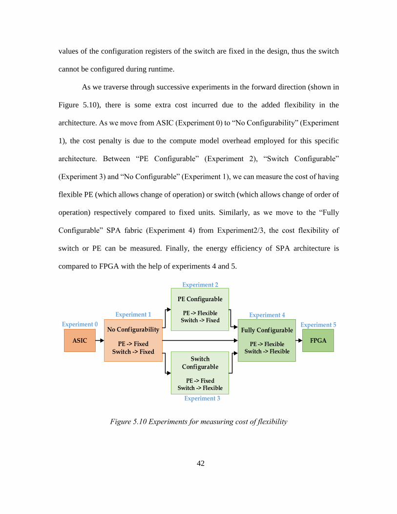
The exact cost of flexibility is determined by removing the programmability from
PEs and Switches. The experiments are summarized in Figure 5.10. A fixed PE supports
only a single function and is not configurable during runtime. Fixed switch means that the
25
26
27
28
29
30
31
32
33
34
35
36
0.4 0.6 0.8 1 1.2 1.4 1.6 1.8 2 2.2 2.4 2.6
En
erg
y (
pJ
)
Time Period (ns)
42
values of the configuration registers of the switch are fixed in the design, thus the switch
cannot be configured during runtime.
As we traverse through successive experiments in the forward direction (shown in
Figure 5.10), there is some extra cost incurred due to the added flexibility in the
architecture. As we move from ASIC (Experiment 0) to “No Configurability” (Experiment
1), the cost penalty is due to the compute model overhead employed for this specific
architecture. Between “PE Configurable” (Experiment 2), “Switch Configurable”
(Experiment 3) and “No Configurable” (Experiment 1), we can measure the cost of having
flexible PE (which allows change of operation) or switch (which allows change of order of
operation) respectively compared to fixed units. Similarly, as we move to the “Fully
Configurable” SPA fabric (Experiment 4) from Experiment2/3, the cost flexibility of
switch or PE can be measured. Finally, the energy efficiency of SPA architecture is
compared to FPGA with the help of experiments 4 and 5.
No Configurability
PE -> FixedSwitch -> Fixed
PE Configurable
PE -> FlexibleSwitch -> Fixed
Switch Configurable
PE -> FixedSwitch -> Flexible
Fully Configurable
PE -> FlexibleSwitch -> Flexible
Experiment 1
Experiment 2
Experiment 3
Experiment 4
ASIC FPGA
Experiment 0 Experiment 5
Figure 5.10 Experiments for measuring cost of flexibility

43
5.2.2. Application results
The results for four image-processing applications are obtained on this architecture.
Applications are: Canny1 edge detection [Canny86], Harris2 corner detection [Harris88],
FAST corner detection [Durand02] and Convolution3 for 5x5 window. Wave pipeline
topology is used for the edge detection applications. The memory costs and the ASIC
results are obtained from Brunhaver’s work [Brun15]. The line buffer data are obtained
from Cacti [Mura09]. The FPGA4 result is in 28nm technology node, while all other results
are obtained using 45nm cell library. The results are shown in Figure 5.11 and Figure 5.12.
As we move from ASIC to different configurations of SPA, the energy cost
increases with each successive experiments. The energy cost is higher for having a
programmable switch (“Switch Configurable”) than having a programmable PE (“PE
Configurable”) compared to both as fixed units (“No Configurability”). We observe a
similar trend in area cost except the results for Harris application. This is due to the use of
multipliers that account for a larger area in PEs. If we take the arithmetic mean of the results
for the four applications, SPA is 4.1X energy expensive and ~5.9X area expensive
compared to ASIC. These results account for the optimized implementations of the
applications in the SPA fabric. For instance, any kernel has the exact same size of the fabric
(stage-height and stage-width of wave pipeline topology) that is necessary to implement
1 The hysteresis stage of Canny is not implemented.
2 The ASIC version utilized 32-bit operations, whereas SPA uses 16-bit operations.
3 The ASIC and FPGA results for convolution are for the 3-channel image, whereas the SPA results are for
a single-channel convolution.
4 The throughput of the FPGA designs is ~10 cycles per pixel.

44
that specific kernel. In addition, a kernel only supports the functions that are required by
that specific kernel. There will be some extra area and energy cost when different
applications share the same kernels.
FPGA is 1.6X energy expensive than SPA and 6.6X energy expensive than ASIC
implementation based on the arithmetic mean of the results for the applications. However,
the FPGA results are obtained on 28nm technology node, whereas SPA/ASIC results are
obtained using 45nm cell library. Considering the scaling factor, the current FPGA results
might be four times worse in 45nm technology node.
Figure 5.11 Energy results for applications
0
1
2
3
4
5
6
7
8
Convolution_5x5 Canny Harris FAST
En
erg
y/O
p i
n p
J/o
p
Applications
ASIC No configurability PE configurable
Switch configurable SPA FPGA*

45
Figure 5.12 Area results for the applications
The categorization of energy and area costs that account for PEs, switches, etc. is
shown in Figure 5.13 and Figure 5.14 for all the four types of experiments. Total energy
cost for each of the applications is represented as the sum of the energy cost of PEs, energy
cost of switches, clock-tree energy and the remaining energy incurred at top level design.
Similarly, the total area cost is represented as the sum of area cost of PEs and switches.
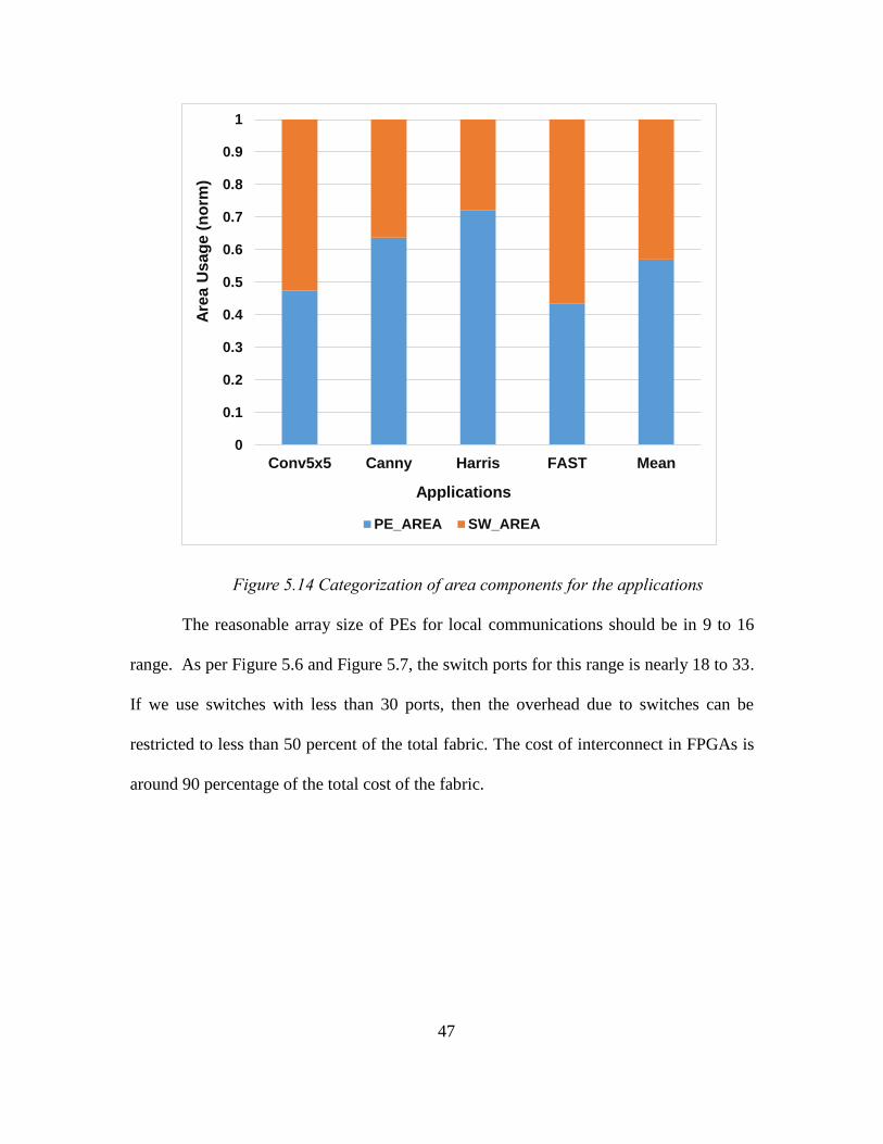
The mean energy of switch is 35 percent and the mean area of the switch is 43
percent for all the applications in the fully configurable experiment. The mean energy of
PEs is 46 percent and the mean area of the PEs is 57 percent for all the applications in the
fully configurable experiment. The average clock-tree energy is nearly 17 percent of the
total energy of the SPA fabric for the applications.
0
2
4
6
8
10
12
Convolution_5x5 Canny Harris FAST
Are
a/P
erf
/Op
in
mm
2/(
op
/ps)
Applications
ASIC No configurability PE configurable Switch configurable SPA

46
Figure 5.13 Categorization of energy components for the applications
5.3. Conclusions from the result
For efficient computation, the hardware should be tailored to match the actual data
precision in the application. The image processing applications essentially perform 8-bit or
16-bit operations for different kernels. From the experimental results (Sec 5.1.1), it is
evident that this architecture is optimum for the 8-bit or 16-bit precision of operation.
Hence, these applications can be efficiently implemented on this architecture. Again,
Genesis2 parameters can be used to alter the precision of the hardware so that it matches
the data precision in the applications.
0
0.1
0.2
0.3
0.4
0.5
0.6
0.7
0.8
0.9
1
Conv5x5 Canny Harris FAST Mean
En
erg
y U
sag
e (
no
rm)
Applications
PE_ENERGY SW_ENERGY CLK_ENERGY TOP_ENERGY
47
Figure 5.14 Categorization of area components for the applications
The reasonable array size of PEs for local communications should be in 9 to 16
range. As per Figure 5.6 and Figure 5.7, the switch ports for this range is nearly 18 to 33.
If we use switches with less than 30 ports, then the overhead due to switches can be
restricted to less than 50 percent of the total fabric. The cost of interconnect in FPGAs is
around 90 percentage of the total cost of the fabric.
0
0.1
0.2
0.3
0.4
0.5
0.6
0.7
0.8
0.9
1
Conv5x5 Canny Harris FAST Mean
Are
a U
sag
e (
no
rm)
Applications
PE_AREA SW_AREA

48
CHAPTER 6. CONCLUSION AND FUTURE WORK
6.1. Thesis Summary and Conclusion
In this work, the proposed data path architecture is designed to be energy efficient,
programmable, easy to program for image processing applications. This architecture
achieves its energy efficiency by exploiting the significant locality present image
processing applications.
This architecture is an optimization of FPGA by means of coarse-grained approach
and the use of local interconnect. This work verifies that the precision of operation
employed in image processing applications is indeed optimum for this coarse-grained
fabric.
The primary objective of this work is to analyze the feasibility of the architecture
in terms of its functionality and energy efficiency, for image processing applications. The
application results show that this architecture is only within a single order of magnitude
energy and area expensive compared to ASIC implementations.
6.2. Scope of Future work
While this thesis has demonstrated the feasibility and working of this architecture
for image processing applications, still there are numerous ways to improve the architecture
further. Some of these are mentioned in the following paragraphs.
The switches can be de-featured to support a specific set of connections, which
apply to the data-flow structure of the algorithm. Practically, the fully connected switches
are not always desirable for many applications and are costly in terms of area and energy.
This can significantly reduce the cost of the overall interconnect fabric and can further
reduce the routing overhead of the architecture.

49
Further efficiency can be gained by employing heterogeneous PEs that are
specifically customized according to the functions used in applications. For instance,
multiplication is an expensive operation performed in a PE. If multiplication is used only
at certain stages of the data flow of the algorithm, it should not be supported in the PEs for
other stages. This enables this architecture to further approach ASIC’s efficiency.
Hierarchical local interconnect approach can be analyzed for further efficiency.
This is especially applicable for applications that require local communication among a
large number of computational units. In this work, the size of local communication is
analyzed only on a single switch. The exact structure of the hierarchical interconnect, and
its cost for different configurations need to be analyzed for different applications.

50
REFERENCES
[Mark06] D. Markovic, B. Nikolic, and R.W. Brodersen, “Power and area efficient vlsi
architectures for communication signal processing,” In Communications, 2006. ICC ’06.
IEEE International Conference on, volume 7, pages 3223–3228, June 2006.
[Horo14] Mark Horowitz, “Keynote: Computing’s energy problem and what we can do
about it,” ISSCC ’14: International Solid State Circuit Conference, June 2014.
[Moore65] Gordon Moore, “Cramming More Components onto Integrated Circuits,”
Electronics Magazine, 38(8), April 1965.
[Ratt02] Justin Rattner, “Making the right hand turn to power efficient computing,” in
35th Microarchitecture Symposium, keynote address, November 2002.
[Pathak11] A. Pathak, Y. C. Hu, M. Zhang, P. Bahl, and Y.-M. Wang, “Fine-grained power
modeling for smartphones using system call tracing,” in Proceedings of the Sixth
Conference on Computer Systems, ser. EuroSys ’11. New York, NY, USA: ACM, 2011,
pp. 153–168. [Online]. Available: http: //doi.acm.org/10.1145/1966445.1966460.
[ITRS10] ITRS, “Overall technology roadmap characteristics,” International Technology
Roadmap for Semiconductors, 2010. http://www.itrs.net.
[Cunn14] Andrew Cunningham, “Broadwell is coming: A look at intel's low-power core
m and its 14nm process,” ArsTechnica, 2014.
[Dent16] Steve Dent, “Intel is officially slowing down the pace of CPU releases,” 2016
http://www.engadget.com/2016/03/23/intel-eliminating-tick-tock-moores-law/.
[Denn99] R.H. Dennard, F.H. Gaensslen, H.N. Yu, V.L. Rideout, E. Bassous, and A.R.
LeBlanc, “Design of ion-implanted MOSFET’s with very small physical dimensions,”
Proceedings of the IEEE (reprinted from IEEE Journal Of Solid-State Circuits, 1974),
87(4):668–678, 1999.
[Cour13] R. Courtland, “The end of the shrink,” Spectrum, IEEE, 50(11):26–29, November
2013.
[Ahmed11] K. Ahmed and K. Schuegraf, “Transistor wars,” Spectrum, IEEE, 48(11):50–
66, November 2011.
[Chen14] Yunji Chen, Tao Luo, Shaoli Liu, Shijin Zhang, Liqiang He, Jia Wang, Ling Li,
Tianshi Chen, Zhiwei Xu, Ninghui Sun, and O. Temam, “Dadiannao: A machine-learning
supercomputer,” In Microarchitecture (MICRO), 2014 47th Annual IEEE/ACM
International Symposium on, pages 609–622, Dec 2014.
[Mark12] Dejan Markovic and Robert W. Brodersen, “DSP Architecture Design
Essentials,” Springer Publishing Company, Incorporated, 2012.

51
[Qadeer13] Wajahat Qadeer, Rehan Hameed, Ofer Shacham, Preethi Venkatesan, Christos
Kozyrakis, and Mark A. Horowitz, “Convolution engine: Balancing efficiency &
flexibility in specialized computing,” SIGARCH Computer Architecture News, 41(3):24–
35, June 2013.
[Kuon07] Ian Kuon and J. Rose, “Measuring the gap between FPGAs and ASICs,”
Computer-Aided Design of Integrated Circuits and Systems, IEEE Transactions on,
26(2):203–215, Feb 2007.
[Sites96] R. Sites, “It’s the memory, stupid!,” In Microprocessor Report, volume 10, pages
1–2, Aug 1996.
[Nowa96] A. Nowatzyk, Fong Pong, and A. Saulsbury, “Missing the memory wall: The
case for processor/memory integration,” In Computer Architecture, 1996 23rd Annual
International Symposium on, pages 90–90, May 1996.
[Lee14] Hyoukjoong Lee, K.J. Brown, A.K. Sujeeth, T. Rompf, and K. Olukotun,
“Locality-aware mapping of nested parallel patterns on GPUs,” Proceedings of the 47th
Annual IEEE/ACM International Symposium on Microarchitecture (MICRO), December
2014.
[Govind12] Venkatraman Govindaraju, Chen-Han Ho, Tony Nowatzki, Jatin Chhugani,
Nadathur Satish, Karthikeyan Sankaralingam, and Changkyu Kim, “Dyser: Unifying
functionality and parallelism specialization for energy-efficient computing,” IEEE Micro,
32(5):38–51, September 2012.
[Govind11] V. Govindaraju, Chen-Han Ho, and K. Sankaralingam, “Dynamically
specialized datapaths for energy efficient computing,” 2011 IEEE 17th International
Symposium on High Performance Computer Architecture(HPCA), pages 503–514, Feb
2011.
[Pedram12] A. Pedram, R.A. van de Geijn, and A. Gerstlauer, “Codesign tradeoffs for
high-performance, low-power linear algebra architectures,” Computers, IEEE
Transactions on, 61(12):1724–1736, Dec 2012.
[Kung79] H.T. Kung and C.E. Leiserson, “Systolic arrays (for vlsi),” Sparse Matrix
Proceedings, 1979.
[Hameed10] Rehan Hameed, Wajahat Qadeer, Megan Wachs, Omid Azizi, Alex
Solomatnikov, Benjamin C.Lee, Stephen Richardson, Christos Kozyrakis, and Mark
Horowitz, “Understanding sources of inefficiency in general-purpose chips,” In
Proceedings of the 37th annual international symposium on Computer architecture, ISCA
’10, pages 37–47, New York, NY, USA, 2010. ACM.
[Mura09] Naveen Muralimanohar and Rajeev Balasubramonian, “CACTI 6.0: A tool to
understand large Caches,” 2009.

52
[Para13] Angshuman Parashar, Michael Pellauer, Michael Adler, Bushra Ahsan, Neal
Crago, Daniel Lustig, Vladimir Pavlov, Antonia Zhai, Mohit Gambhir, Aamer Jaleel,
Randy Allmon, Rachid Rayess, Stephen Maresh, and Joel Emer, “Triggered instructions:
A control paradigm for spatially-programmed architectures,” SIGARCH Comput. Archit.
News, 41(3):142–153, June 2013.
[Kung86] H. T. Kung, “The CMU Warp Processor,” In F. A.Matsen and T. Tajima editors,
Supercomputers: Algorithms, Architectures, and Scientific Computation, pages 235–247.
1986.
[Borkar90] S. Borkar, R. Cohn, G. Cox, T. Gross, H. T. Kung, M. Lam, M. Levine, B.
Moore, W. Moore, C. Peterson, J. Susman, J. Sutton, J. Urbanski, J. Webb, “Supporting
Systolic and Memory communication in iWarp,” Proc. 17th Int’l Symp, Computer
Architecture, IEEE CS Press, Los Alamitos, California, 1990, pp. 70-81.
[Cota15] E.G. Cota, P. Mantovani, G. Di Guglielmo, and L.P. Carloni, “An analysis of
accelerator coupling in heterogeneous architectures,” In Design Automation Conference
(DAC), 2015 52nd ACM/EDAC/IEEE, pages 1–6, June 2015.
[Brun15] John Brunhaver, “Design and Optimization of a Stencil Engine,” Ph.D. thesis,
STANFORD UNIVERSITY, 2015.
[Hame10] R. Hameed, W. Qadeer, M. Wachs, O. Azizi, A. Solomatnikov, B. C. Lee, S.
Richardson, C. Kozyrakis, and M. Horowitz, “Understanding Sources of Inefficiency in
General-Purpose Chips,” In ISCA ’10: Proc. 37th Annual International Symposium on
Computer Architecture. ACM, 2010.
[Yuan15] Fang-Li Yuan, C.C. Wang, Tsung-Han Yu, and D. Markovic, “A multi-
granularity FPGA with hierarchical interconnects for efficient and flexible mobile
computing,” Solid-State Circuits, IEEE Journal of, 50(1):137–149, Jan 2015.
[Comp02] K. Compton and S. Hauck, “Reconfigurable Computing: A Survey Of Systems
and Software,” ACM Computer Survey, 34(2):171–210, June 2002.
[Marq00] A. Marquardt, V. Betz, and J. Rose, “Speed and Area Tradeoffs in Cluster-Based
FPGA Architectures,” IEEE Transactions on Very Large Scale Integration (VLSI) Systems,
8(1):84 –93, Feb. 2000.
[Shac11] Ofer Shacham, “CHIP MULTIPROCESSOR GENERATOR: AUTOMATIC
GENERATION OF CUSTOM AND HETEROGENEOUS COMPUTE
PLATFORMS,” Ph.D. thesis, STANFORD UNIVERSITY, 2011.
[Shac15] Ofer Shacham. Genesis2. http://genesis2.stanford.edu/, January 2015.
[Shac10] Ofer Shacham, Omid Azizi, Megan Wachs, Stephen Richardson, and Mark
Horowitz, “Rethinking digital design: Why design must change”, IEEE Micro, 30(6):9–
24, November 2010.
53
[Hega14] James Hegarty, John Brunhaver, Zachary DeVito, Jonathan Ragan-Kelley, Noy
Cohen, Steven Bell, Artem Vasilyev, Mark Horowitz, and Pat Hanrahan, “Darkroom:
Compiling high-level image processing code into hardware pipelines,” ACM Trans.
Graph., 33(4):144:1–144:11, July 2014.
[Canny86] John Canny, “A computational approach to edge detection,” PAMI-8(6):679–
698, November 1986.
[Harris88] Chris Harris and Mike Stephens, “A combined corner and edge detector,” In
Proc. of Fourth Alvey Vision Conference, pages 147–151, 1988.
[Durand02] Fr´edo Durand and Julie Dorsey, “Fast bilateral filtering for the display of
high-dynamic range images,” ACM Trans. Graph., 21(3):257–266, July 2002.
[Ruetz86] P. Ruetz and R. Brodersen, “A real-time image processing chipset,” In Solid-
State Circuits Conference. Digest of Technical Papers. 1986 IEEE International, volume
XXIX, pages 148–149, Feb 1986.
[Kamp90] W. Kamp, R. Kunemund, H. Soldner, and R. Hofer, “Programmable 2d linear
filter for video applications,” Solid-State Circuits, IEEE Journal of, 25(3):735–740, Jun
1990.
[Zehner86] Bernd Zehner, H. Mattausch, F. Matthiesen, R. Tielert, and H.-J. Grallert, “A
CMOS vlsi chip for filtering of tv pictures in two dimensions,” Solid-State Circuits, IEEE
Journal of, 21(5):797–802, Oct 1986.
[Kung79] H.Kung and C.Leiserson,“Systolic arrays (for vlsi),” Sparse Matrix
Proceedings,1979.
[Kung88] S.Y.Kung, “VLSI array processors,” Englewood Cliffs, NJ: Prentice
Hall, 1988.
[Coll60] L. Collatz, “The Numerical Treatment of Differential Equations,” ser.
Grundlehren der mathematischen Wissenschaften. SpringerVerlag, 1960. [Online].
Available:http://books.google.com/books?id=Fr7QAAAAMAAJ
[Ragan12] J.Ragan-Kelley, A.Adams, S.Paris, M.Levoy, S.Amarasinghe and F.Durand,
“Decoupling algorithms from schedules for easy optimization of image processing
pipelines,”ACM Transactions on Graphics, vol. 31, no. 4, Jul. 2012. [Online].
Available:http://groups.csail.mit.edu/commit/papers/2012/ragan-kelley-siggraph12-
halide.pdf
[Venkat10] G. Venkatesh, J. Sampson, N. Goulding, S. Garcia, V. Bryksin, J. Lugo-
Martinez, S. Swanson, and M. B. Taylor, “Conservation cores: reducing the energy of
mature computations,” SIGARCH Comput. Archit. News, vol. 38, no. 1, pp. 205–218, Mar.
2010. [Online]. Available: http://doi.acm.org/10.1145/1735970.1736044
54
[Dennis75] Jack B. Dennis and David P. Misunas, “A preliminary architecture for a basic
data-flow processor,” In Proceedings of the 2Nd Annual Symposium on Computer
Architecture, ISCA ’75, pages 126–132, New York, NY, USA, 1975. ACM.
[Todman05] T.J. Todman, G.A. Constantinides, S. J E Wilton, O. Mencer, W. Luk, and P.
Y K Cheung, “Reconfigurable computing: architectures and design methods,” Computers
and Digital Techniques, IEE Proceedings -, 152(2):193–207, Mar 2005.
[Bols06] I. Bolsens, “Programming modern FPGAs,” Int. Forum on Embedded
Multiprocessor SoC, Keynote, Aug. 2006.
[Merr13] R. Merritt, “FPGA add comms cores amid ASIC debate,” EE Times, Mar. 2013.
[Taylor02] M. Taylor, J. Kim, J. Miller, D. Wentzlaff, F. Ghodrat, B. Greenwald, H.
Hoffman, P. Johnson, J. Lee, W. Lee, et al. “The Raw Microprocessor: A Computational
Fabric for Software Circuits and General-Purpose Programs,” IEEE Micro, 22(2):25–35,
2002.
[Copen99] Seth Copen, Goldstein Herman, Schmit Matthew, Moe Mihai, Budiu Srihari
Cadambi, R. Reed, Taylor Ronald Laufer, “PipeRench: A Coprocessor for Streaming
Multimedia Acceleration,” Proceedings of 26th International Symposium on Computer
Architecture, ISCA 1999.
[IEEE09] Ieee standard for SystemVerilog unified hardware design, specification, and
verification language. IEEE STD 1800-2009, pages C1 –1285, 200.
[Adams10] A. Adams, E.-V. Talvala, S. H. Park, D. E. Jacobs, B. Ajdin, N. Gelfand, J.
Dolson, D. Vaquero, J. Baek, M. Tico, H. P. A. Lensch, W. Matusik, K. Pulli, M. Horowitz,
and M. Levoy, “The Frankencamera: an experimental platform for computational
photography,” in ACM SIGGRAPH 2010 papers. New York, NY, USA: ACM, 2010, pp.
29:1–29:12. [Online]. Available:http://doi.acm.org/10.1145/1833349.1778766.
[Suger09] J. Sugerman, K. Fatahalian, S. Boulos, K. Akeley, and P. Hanrahan, “Gramps:
A programming model for graphics pipelines,” ACM Trans. Graph., vol. 28, no. 1, pp. 4:1–
4:11, Feb.2009. [Online]. Available: http://doi.acm.org/10.1145/1477926.1477930.
[Thies02] W. Thies, M. Karczmarek, and S. P. Amarasinghe, “StreamIt:A language for
streaming applications,” in Proceedings of the 11th International Conference on Compiler
Construction, ser. CC ’02.London, UK, UK: Springer-Verlag, 2002, pp. 179–196.
[Online].Available: http://dl.acm.org/citation.cfm?id=647478.727935.
[Kapa03] U. J. Kapasi, S. Rixner, W. J. Dally, B. Khailany, J. H. Ahn, P. Mattson, and J.
D. Owens, “Programmable stream processors,” vol. 36, no. 8, pp. 54–62, Aug. 2003.
[Online]. Available:http://dx.doi.org/10.1109/MC.2003.1220582.

55
[Ragan13] J. Ragan-Kelley, C. Barnes, A. Adams, S. Paris, F. Durand, and S. Amarasinghe,
“Halide: A language and compiler for optimizing parallelism, locality and recomputation
in image processing pipelines,” in ACM SIGPLAN Conference on Programming
Language Design and Implementation, San Jose, CA, Jun. 2013.
[Lee11] H. J. Lee, K. Brown, A. Sujeeth, H. Chafi, K. Olukotun, T. Rompf, and M. Odersky,
“Implementing domain-specific languages for heterogeneous parallel computing,” Micro,
IEEE, vol. 31, no. 5, pp. 42–53, 2011.
[George14] N. George, H. Lee, D. Novo, T. Rompf, K. Brown, A. Sujeeth, M. Odersky, K.
Olukotun, and P. Ienne, “Hardware system synthesis from domain-specific languages,” in
Field Programmable Logic and Applications (FPL), 2014 24th International Conference
on, Sept 2014, pp. 1–8.
[Volp85] Dennis M. Volpano and Richard B. Kieburtz. Software templates. In Proceedings
of the 8th International Conference on Software Engineering, ICSE ’85 pages 55–60, Los
Alamitos, CA, USA, 1985. IEEE Computer Society Press.
[Krue92] Charles W. Krueger. Software reuse. ACM Comput. Surv., 24(2):131–183, June
1992.
[Perl16] Perl. http://www.perl.org, 2016.
[Mack16] Curtis Mackay, ”The feasibility of domain specific compilation for spatially
programmable architectures ”, Master’s thesis, Arizona State University, 2016 (To be
published).
[Arvind86] Arvind and D. E. Culler, “Dataflow architectures”, chap. Annual review of
computer science vol. 1, 1986, pp. 225–253 (Annual Reviews Inc., Palo Alto, CA, USA,
1986).
[Galal13] S. Galal, O. Shacham, J.S. Brunhaver, Jing Pu, A. Vassiliev, and M. Horowitz.
Fpu generator for design space exploration. In Computer Arithmetic (ARITH), 2013 21st
IEEE Symposium on, pages 25–34, April 2013.
[Wachs14] Meghan Wachs. Specifying and Validating Memory Protocols for Chip
Generators. Ph.D. thesis, STANFORD UNIVERSITY, 2014.