Embed Size (px)
Citation preview

Circuits for Data Converters
Data Converters
Pietro AndreaniDept. of Electrical and Information Technology
Lund University, Sweden
Overview
• Sample-and-Hold (S&H)• Diode bridge S&H• Switched emitter follower• BJT S&H • CMOS S&H• CMOS switch with low supply voltage
Data Converters Circuits for Data Converters 2
• CMOS switch with low supply voltage• Folding amplifiers• Voltage-to-current converters• Clock generation
Sample-and-Hold
The S&H uses two phases one for sampling, one for retaining and making the signal available to the following circuits (hold phase)
The input buffer reduces the input load, and the output buffer avoids discharging the sampling capacitance
If the output is available during the sampling period, we have a track-and-hold (T&H)
Data Converters Circuits for Data Converters 3
Diode bridge S&H
Schottky diodes very fast multi-GHz rates
During sampling (tracking, actually), I1=I2 flows into the diode bridge, and Vin is copied onto Cs – if the current from Vin is small compared to I1, we can use the small-signal linear circuit of the diode bridge as below if gm/Cs is much larger than the signal frequency, V(Cs)= Vin
During hold, no current flows through the bridge, and Cs stores the sampled signal – a unity-gain buffer is then cascaded as usual
sC
mg
mg mg
mg
inV
Data Converters Circuits for Data Converters 4

Diode bridge – non-idealities
If I1 > I2 current difference flows into the signal source during sampling, but during hold brings I1 towards triode voltage at B increases, D2 can enter conduction and corrupt the sampled signal it is important to have I1 < I2, which brings node B down and does not cause any harm
Data Converters Circuits for Data Converters 5
Other non-idealities
Aperture distortion error in the switching-off time, caused by the derivative of the input signal a varying input voltage delivers a current to Cs a positive derivative makes the current through D1 and D4 lower than in the other pair, leading to an asymmetrical bridge current non-linear error in the switching instant
Tack-mode distortion caused by the non-linear impedance of the input buffer driving the bridge since the non-linear voltage drop is proportional to the current , i.e. voltage derivative, this distortion increases with frequency
1C s inI C dV dt= ⋅
Data Converters Circuits for Data Converters 6
increases with frequency
Hold pedestal given by the (non-linear) charge injected by the diodes from on to off
Hold feed-through caused by parasitic coupling between input and output during hold (diodes are par. caps when off)
Improved diode bridge
The two extra diodes DA and DB are reverse-biased (by D2 and D4 conducting) during Tracking, but are turned on by the two Ix during Hold, clamping B and A at ±VD (≈ ±0.7V) constant biasing of D1 and D2 results in constant hold pedestal
A and B are biased through the load impedance of the buffer, and the conducting diodes DA and DB have a low impedance of 1/gm RA and RB are much reduced decoupling of input from CS much reduced feedthrough
Data Converters Circuits for Data Converters 7
feedthrough
A H D
B H D
V V V
V V V
= += −
HV
Switched emitter follower
Reduced requirements from power supply (0.7V saved); circuit on the right diminishes the input current load by the BJT gain
Major drawback requires simultaneous switching-off of both current sources to prevent spur injection into Cs (1ps delay with 1pF and 1mA 1mV offset)
Impossible to align very well the two clock signals Self synchronization required
Data Converters Circuits for Data Converters 8
input current reduction
Improved version
QE is an emitter follower during sampling; when ΦH goes high and ΦSlow, Ibias flows through Rb and VB is pulled down, but the emitter of QE is kept high by CS QE is switched off
The voltage on CS is a shifted replica of the input usually not a problem, as the DC component is not interesting
However, CBE in QE causes a hold pedestal that depends on the reversed VBE during hold uncontrolled VB, unpredictable pedestal
Data Converters Circuits for Data Converters 9
Improved – II
Left: QC replicates the held voltage and clamps VB during hold constant VBE = constant pedestal; during tracking QC goes off and does not influence operations
Other source of pedestal: charge injection from base and collector of QSand QH QS matched by dummy transistors QD1 and QD2 (right) driven by complementary phases; back-to-back diode D1 and D2 match the non-linear CBE from QE
Data Converters Circuits for Data Converters 10
Input buffers
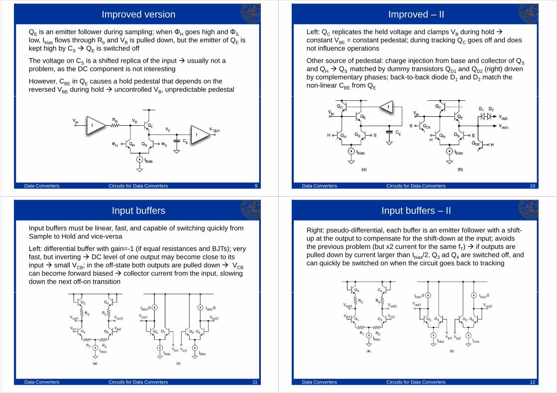
Input buffers must be linear, fast, and capable of switching quickly from Sample to Hold and vice-versa
Left: differential buffer with gain=-1 (if equal resistances and BJTs); very fast, but inverting DC level of one output may become close to its input small VCB; in the off-state both outputs are pulled down VCBcan become forward biased collector current from the input, slowing down the next off-on transition
Data Converters Circuits for Data Converters 11
Input buffers – II
Right: pseudo-differential, each buffer is an emitter follower with a shift-up at the output to compensate for the shift-down at the input; avoids the previous problem (but x2 current for the same fT) if outputs are pulled down by current larger than Ibias/2, Q3 ad Q4 are switched off, and can quickly be switched on when the circuit goes back to tracking
Data Converters Circuits for Data Converters 12

Complementary BJT S&H
If npn and pnp have comparable fT (however, not usual!) circuit (a) implements the DC shift in the previous slide; (b) push-pull implementation – with equal npn (pnp) areas and I1=I2, bias output current is I1; during transients, one output transistor reduces its VBE, making it available for the other; if one goes off, all current through the other transistor flows through the output (class B)
(c): switched buffer QS1/QH1 (QS2/QH2) divert I1 (I2) from the emitter of Q1 (Q3) (CL clamping block; sources/sinks I1/I2 during Hold)
Data Converters Circuits for Data Converters 13
Q1 (Q3) (CL clamping block; sources/sinks I1/I2 during Hold)
Features of BJT S&H
Good speed and linearity, but limited dynamic range (junctions must be kept in reverse in the off-state) – consider the buffer/S&H below:
( )in DV nT V−
( ) 2in DV nT V−
( )inV t
( )in DV t V−
Data Converters Circuits for Data Converters 14
Hold Q4 is in reverse; emitter of Q4 follows the input via Q2, the limit to the input voltage swing is (assuming a differential input signal ):
Maximum change of full-range sine wave (at Nyquist) is Vref/2 over the time T/2 maximum input amplitude cannot exceed 2VD
( ) ( ) ( ) for 2in D in in DV nT V V t V nT V nT t nT T− < < + < < +
hold instants hold period
inV±
S&H non-linearity
0 ln EBE BE T
bias
IV V V
I≈ +Depends on the non-linear VBE-IE relation
IE is the sum of Ibias and the current into Cs:
In a pseudo-differential circuit, we have
inE bias S
dVI I C
dt≈ +
in inbias S bias S
dV dVI C I C+ −
Data Converters Circuits for Data Converters 15
resulting in the error on the differential output:
0 0ln ; lnbias S bias S
out in BE T out in BE Tbias bias
I C I Cdt dtV V V V V V V V
I I+ + − −
+= − − = − −
, ln
inbias S
out d Tin
bias S
dVI C
dtV VdV
I Cdt
δ+
=−
S&H non-linearity – II
With an input , we obtain
odd function only odd harmonics, with amplitude proportional to input amplitude and frequency, and sampling capacitance
( )sinin inV A tω=
( )( ),
cosln
cosbias in S in
out d Tbias in S in
I A C tV V
I A C t
ω ωδ
ω ω+
=−
Data Converters Circuits for Data Converters 16
To minimize bias current should be much larger than current into sampling capacitance
Example: if Cs = 4pF, fin = 200MHz, A = 1V ICs up to 5mA
It can be shown that SFDR=100dB requires Ibias ≈ 8ICs Ibias = 40mA

Noise in emitter follower
2 44
kTv kTr
γ,4 m biaskT gγ
Important: this part is wrong in the book
Channel noise factor 2/3 for ideal MOS, 1/2 for ideal BJT
In (d) below a large RS in series with switch trades reduced speed for reduced total noise power, which tends to the minimum limit of for large (impact of is minimized)
SkT Cm sg R 'bb
r
γ
Data Converters Circuits for Data Converters 17
'
'
2,
,2, 2
44
444
n in bbm
m biasn eq bb
m m
kTv kTr
g
kT gkTv kTr
g g
γ
γγ
= +
≈ + +
2,
4n eq
m
kTv
gγ′= 2
, 1S
m sn C
S m s
g RkTV
C g R
γ′+=+
dsrdsr
CMOS S&H
Time constant much lower than time allowed for charging
If switched voltage has a large range use nMOS and pMOS in parallel total resistance is ideally constant over a large voltage range
Dummy MD clock feedthrough compensation
(c) uses a simple source follower for maximizing speed (GHz range) bad linearity, even with B=S to avoid non-liner bulk effect (max. 70dB, compared to 100dB with BJT for the same current)
on SR C SC
Data Converters Circuits for Data Converters 18
compared to 100dB with BJT for the same current)
onox od
LR
C WVμ=
pseudo differential
Clock feedthrough
When MOS from on to off, due to: 1) channel charge flowing into CS, and 2) clock charge injection through Cgd – the fraction of injected into CS depends on a) MOS parameters, b) slope of the clock phase, c) boundary conditions on both sides of the switch
Charge injection studied with simplified RC model for both gate and channel; numerical solutions as function of the switching parameter B:
chQchQ
C W L
Data Converters Circuits for Data Converters 19
ch ox odQ C WLV=
GdV
dtα =
oxod
S
C W LB V
C
μα
=
Clock feedthrough - II
low B (i.e. fast switching) 50% of channel charge flows into sampling capacitance
large B depends on ratio between the two capacitances less predictable
low B is more predictable preferred
Data Converters Circuits for Data Converters 20

Feedthrough compensation
Dummy MD injects all its channel charge into CS should be approx. half as large as the switch this asymmetry reduces effectiveness of cancellation to 70-80%
In differential A/D differential cancellation of injection common-mode injection is suppressed by the differential topology, as in (a) below –effectiveness of 80-90%
Another approach is to accept a constant injection = constant offset, as in (b) not an issue if there is no signal at DC
Data Converters Circuits for Data Converters 21
(b) not an issue if there is no signal at DC
Feedthrough compensation - II
(b) constant injection if constant channel charge and constant voltage node A is switched between ground and virtual ground charge
injected into virtual ground depend on charge injected into A when S3opens same boundary conditions must exist in all clock periods
Contemporary switching of the two sides of CS is avoided by opening S1slightly later than S3 – the plate connected to ground determines the actual sampling (bottom-plate sampling technique)
Data Converters Circuits for Data Converters 22
Two-stage OTA as T&H
Output of two-stage OTA in unity-gain feedback tracks input 1st stage output is input divided by 2nd stage gain ( (a) below)
Compensation capacitor in OTA can be used as sampling capacitor as well CC becomes CS in (b) – voltage at the end of tracking is
V1 is (almost) zero if A2 large constant channel charge feedthrough
( ) ( )( ) ( ) ( )1 21
1 2 2
01
in os outout
V nT V AA V nTV nT V nT
AA A
+= = ≈
+
Data Converters Circuits for Data Converters 23
V1 is (almost) zero if A2 large constant channel charge feedthrough is just an offset; 1st stage not used during Hold offset auto-zeroing is possible (connect as unity gain buffer, store offset onto a capacitance)
ok for medium-speed if buffering is needed; also, unity-gain configuration requires common-mode range to be the same as the input swing
1V
Virtual ground in CMOS S&H
In general, virtual ground relieves the requirement of a large input common mode
Charge-transferring S&H below: 1) during Sample, CS are charged between Vin and input common mode VCM,in, CH between input and output common mode VCM,out offset cancellation and possibly common-mode shift; 2) during Hold CS are connected in (anti) series charge transferred to CH, common-mode input is rejected; gain or attenuation possible
Data Converters Circuits for Data Converters 24
possible

Virtual ground in CMOS S&H – II
More economic implementation fewer caps with flip-around topology, where CS is first connected to the input, and then in feedback – however, only unity gain possible – however, feedback factor is 1, while it was ½ in the previous circuit flip-around more power efficient (lower open-loop gain-bandwidth-product required for the same sampling frequency)
Neither scheme uses the op-amp during sampling op-amp is in open-loop output to Vdd or ground, long recovery time differential output is shorted and connected to a common mode voltage during sampling
Data Converters Circuits for Data Converters 25
shorted and connected to a common mode voltage during sampling
Noise analysis of flip-around S&H
Each switch has on-resistance Ron, and a thermal noise voltage of The op-amp has an equivalent input noise voltage
Every noise generator causes a colored noise spectrum across each capacitor; when the switches open, the sampled noise on the capacitor is given by the integral of the colored spectrum
Uncorrelated noise adds power-wise; Correlated adds signal-wise
During Sample, we have the situation in (a) two switches in series with C since the integrated noise is kT/C independently of R, we have
2 4n onv kTR=2,n opv
Data Converters Circuits for Data Converters 26
CS since the integrated noise is kT/C independently of R, we have
during sample
during hold
2,n sample
S
kTV
C=
Noise analysis of flip-around S&H – II
Hold a) the sampled noise on CS is there also during Hold (of course)
Hold b) because of the virtual ground, the noise from the switch in feedback is found at the output, until it rolls off because of the finite bandwidth of the op-amp
,
1
1 1 1T
n out n n nT T
sAv v v v
A s s
ωω ω
= = =+ + +
“signal”
Data Converters Circuits for Data Converters 27
during sample
during hold
( )2 2, ,2
4
1on
n out n out on T
T
kTRv V kTR ω
ω ω= → =
+power
Noise analysis of flip-around S&H – III
2, ,n out flip m on
S L L
kT kT kTV g R
C C C
γ ′= + +
Hold c) The same analysis applies to op-amp noise,
Assuming , we have the total output noise power asmT
L
g
Cω =
2,
4n op
m
kTv
g
γ ′=
Data Converters Circuits for Data Converters 28
during sample
during hold

Noise analysis of flip-around S&H – IV
The sampling time constant RonCS is typically lower than , i.e.
2, ,n out flip m on
S L L
kT kT kTV g R
C C C
γ ′= + +
1 Tω
Lon S
m
CR C
g<<
Data Converters Circuits for Data Converters 29
which means that the second term in the noise expression is negligible
2, ,n out flip
S L
kT kTV
C C
γ ′≈ +
during sample
during hold
Noise analysis of charge-transfer S&H
Sampling charge on CS is later transferred to CH if the charges on the two caps are correlated, linear (signal-wise) addition assuming CS = CH, the transfer function of noise source #3 on both CS and CH is
Considering that during Hold the noise on CS adds signal-wise to the noise on CH, and that this is also the output noise caused by source #3, we have
( ) ( ) ( )1 1
1 3 1 3S HC Con S on S
H s H sR C s R C s
= = =+ +
kT kT
Data Converters Circuits for Data Converters 30
during hold
during sampling
( )22,#3 1 1 4
3 3outS S
kT kTV
C C= + =
Noise analysis of charge-transfer S&H – II
Sampling noise source #1 (and #2) induces a noise voltage across both CS and CH, and noise on CS is subtracted from noise on CH during Hold the relevant transfer function is therefore
Considering that the noise contributions from #1 and #2 add up power-wise, we obtain
( ) ( ) ( ) ( ) ( )1 if
1 3S Heq C C S Hon S
H s H s H s C CR C s
= − = =+
( )2 1 1 2kT kT
V = + =
Data Converters Circuits for Data Converters 31
Hold contributions from #4, #5, and op-amp – #4 is found at the output with gain of -1, band-limited by (-3dB frequency of feedback loop; )
during hold
during sampling
( ),#1 2 1 1 23 3out
S S
VC C+ = + =
Tfβ 1 2β =
Noise analysis of charge-transfer S&H – III
Noise source #5 appears directly at the output, also limited by ; noise from the op-amp is amplified x2, and also limited by
Overall assuming the previous expressions for and , and considering that , the total noise is
2, ,
4 22 4
3 3
2 2 2 2
n out tot on T TS S m
kT kT kTV kTR
C C g
kT kT kT kT kT
γβω βω
γ γ
′= + + ⋅ +
′ ′
TfβTfβ
2,n opv
Tω1 2β =
Data Converters Circuits for Data Converters 32
Therefore, for low noise large capacitances, low-noise op-amp hardly a surprise!
2 2 2 2 m on
S L L S L
kT kT kT kT kTg R
C C C C C
γ γ= + + ≈ +
during hold
during sampling

Example 5.3
Wrong picture in the book! The “reference” noise transfer function is that of the RonCS low-pass filter
Data Converters Circuits for Data Converters 33
offset insensitive flip-around S&H
CMOS pass gate
nMOS gate to Vdd, pMOS to ground maximum conductance, given by
If , the pMOS conductance goes to zero, as does that of the nMOS for . If , the conductance when both MOS are on is independent of , and equal to
, , , , , , on n od n p od p od n dd in th n od p in th pG V V V V V V V V Vβ β= + = − − = −
,in th pV V≤,in dd th nV V V≥ − n pβ β=
inV
( ), ,on n dd th n th pG V V Vβ= − −
Data Converters Circuits for Data Converters 34
CMOS pass gate – II
This means that the conductance decreases with the supply voltage, and can become zero if
Usually, modern processes offer devices with low Vth – however, this increases the cost of the product because of added process steps; it is also possible to use thick-oxide MOS, which allows a (much) higher Vdd (double supply voltage required, extra process step)
, ,dd th n th pV V V≤ +
Data Converters Circuits for Data Converters 35
Switched op-amp technique
Flip-around S&H
Vlow is low no problem driving switch Sb
At the output the whole output op-amp stage is switched off (i.e., the output impedance becomes very high) at nodes close to Vdd and ground no problem
In this way, CS can be connected to the input without disconnecting the OTA with a switch
Data Converters Circuits for Data Converters 36
The only critical element is Sin, whose channel must allocate the whole signal range
Bootstrapping
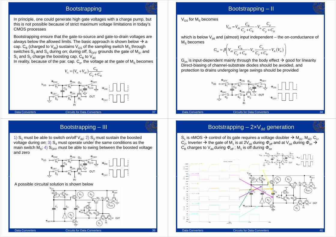
In principle, one could generate high gate voltages with a charge pump, but this is not possible because of strict maximum voltage limitations in today’s CMOS processes
Bootstrapping ensure that the gate-to-source and gate-to-drain voltages are always below the allowed limits. The basic approach is shown below a cap. CB (charged to Vdd) sustains VGS of the sampling switch MS through switches S3 and S4 during on; during off, SOFF grounds the gate of MS, and S1 and S2 charge the boosting cap. CB to Vdd
Data Converters Circuits for Data Converters 37
S1 and S2 charge the boosting cap. CB to VddIn reality, because of the par. cap. Cp, the voltage at the gate of MS becomes
( ) BG in dd
p B
CV V V
C C= +
+
Bootstrapping – II
VGS for MS becomes
which is below Vdd and (almost) input independent – the on-conductance of MS becomes
G is input-dependent mainly through the body effect good for linearity
pBGS dd in
p B p B
CCV V V
C C C C= −
+ +
( )pBon dd in th in
p B p B
CCG V V V V
C C C Cβ⎛ ⎞
= − −⎜ ⎟⎜ ⎟+ +⎝ ⎠
Data Converters Circuits for Data Converters 38
Gon is input-dependent mainly through the body effect good for linearity Direct-biasing of channel-substrate diodes should be avoided, and protection to drains undergoing large swings should be provided
Bootstrapping – III
1) S1 must be able to switch on/off Vdd; 2) S3 must sustain the boosted voltage during on; 3) S4 must operate under the same conditions as the main switch MS; 4) SOFF must be able to swing between the boosted voltage and zero
Data Converters Circuits for Data Converters 39
A possible circuital solution is shown below
Bootstrapping – 2×Vdd generation
S1 is nMOS control of its gate requires a voltage doubler Md1, Md2, C1, C2, Inverter the gate of M1 is at 2Vdd during Φoff and at Vdd during ΦonCB charges to Vdd during Φoff ; M1 is off during Φon
Data Converters Circuits for Data Converters 40

Bootstrapping – more features
Mpo reduces the Vds and Vgd experienced by Mo during Φoff
Body of M3 connected to source no latch-up hazard
Mi3 ensures that VSG3 never exceeds Vdd (Mi1 is cut off when the input voltage IN reaches a value for which Φon – IN < Vth,n)
It is easier to implement M1 as an NMOS than as a PMOS, since a PMOS would start conducting during Φon as soon as IN + Vdd – Vg,M1 (=Vdd) > |Vth,p|
None of the terminal-to-terminal device voltages exceeds V for any device
Data Converters Circuits for Data Converters 41
None of the terminal-to-terminal device voltages exceeds Vdd for any device
Current folding with BJTs
4-segment folding of input current if Iin is zero, two bias currents IE flow into one branch, two into the other the diff. output voltage Vout,d is zero If now 0 < Iin < IE, the current through Q1 is reduced, and we have When Iin becomes higher than IE, the current through Q1 is zero and some current is taken from Q2, obtaining ; when D2 becomes active, the output voltage becomes positive again, to return to negative when D3 is turned on
Notice that the input voltage must increase by one diode voltage for every
,out d L inV R I=
,out d L inV R I= −
Data Converters Circuits for Data Converters 42
Notice that the input voltage must increase by one diode voltage for every active cell dynamic range at input sets the limit to the number of cells
Current folding with MOS
8-segment folding of input current – the use of comparators in more efficient than a diode MOS; the comparator detects an increase of the respective MOS source voltage and turns on the switch – the threshold VBshould be slightly higher than VA-Vtn,h – comparators increase complexity and power consumption, but the voltage drop across the switches is small, and many cells can be cascaded
Data Converters Circuits for Data Converters 43
Voltage folding
Segments (here: 4) generated by the linear region in the transfer function of a differential pair – 2VT for BJT, 2Vod for MOS – too small extended with degeneration resistors by as much as 2ISRD, as the diff. pair becomes fully unbalanced for an input voltage of the differential output voltage changes by
( )S D odI R V± +2 S LI R±
Data Converters Circuits for Data Converters 44
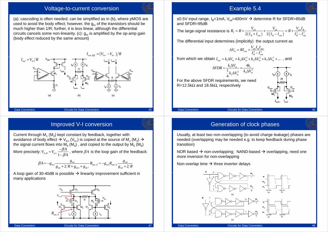
Voltage-to-current conversion
(a): cascoding is often needed; can be simplified as in (b), where pMOS are used to avoid the body effect; however, the gm of the transistors should be much higher than 1/R; further, it is less linear, although the differential circuits cancels some non-linearity. (c): gm is amplified by the op-amp gain (body effect reduced by the same amount)
( ),out diff in inI V V R+ −= −
Data Converters Circuits for Data Converters 45
out inI V R=
Example 5.4
±0.5V input range, IB=1mA, Vod=400mV determine R for SFDR=85dB and SFDR=95dB
The large-signal resistance is
The differential input determines (implicitly) the output current as
from which we obtain , and
( ) ( ) 2 22 2od od od B
TB out B out B out
V V V IR R R
I I I I I I= + + = +
+ − −
2 2od B out
in outB out
V I IV RI
I IΔ = +
−3 5 7 ...I k V k V k V k V
Data Converters Circuits for Data Converters 46
from which we obtain , and
For the above SFDR requirements, we need R=12.5kΩ and 18.5kΩ, respectively
3 5 71 3 5 7 ...out in in in inI k V k V k V k V≈ Δ + Δ + Δ + Δ +
1 12
3 33
414
in
inin
k V kSFDR
k Vk V
Δ≈ =ΔΔ
Improved V-I conversion
Current through M1 (M2) kept constant by feedback, together with avoidance of body effect Vin+ (Vin-) is copied at the source of M1 (M2) the signal current flows into M3 (M4) , and copied to the output by M5 (M6)
More precisely: , where is the loop gain of the feedback:
A loop gain of 30-40dB is possible linearity improvement sufficient in
, 1in R in
AV V
A
ββ+
−≈−
Aβ
1 13 , 3 ,
1 3 7 12 2m m
m out A m out Am ds ds m
g gA g R g R
g R g g g Rβ ≈ − ≈ −
+ + + +
Data Converters Circuits for Data Converters 47
A loop gain of 30-40dB is possible linearity improvement sufficient in many applications
,in RV
,out AR
Generation of clock phases
Usually, at least two non-overlapping (to avoid charge leakage) phases are needed (overlapping may be needed e.g. to keep feedback during phase transition)
NOR based non-overlapping; NAND-based overlapping, need one more inversion for non-overlapping
Non-overlap time three inverter delays
Data Converters Circuits for Data Converters 48