Embed Size (px)
Citation preview

DATA SHEET
Objective specificationFile under Integrated Circuits, IC02
January 1995
INTEGRATED CIRCUITS
Philips Semiconductors
TDA8366I2C-bus controlled PAL/NTSC TVprocessor
January 1995 2
Philips Semiconductors Objective specification
I2C-bus controlled PAL/NTSC TVprocessor
TDA8366
FEATURES
• Multistandard vision IF circuit (positive andnegative modulation)
• Video identification circuit in the IF circuit which isindependent of the synchronization for stable On ScreenDisplay (OSD) under ‘no-signal’ conditions
• Source selection with 2 Colour Video BlankingSynchronization (CVBS) inputs and a Y/C (or extraCVBS) input
• Output signals of the video switch circuit for the teletextdecoder and a Picture-In-Picture (PIP) processor
• Integrated chrominance trap and bandpass filters(automatically calibrated)
• Integrated luminance delay line
• Asymmetrical peaking in the luminance channel with a(defeatable) noise coring function
• PAL/NTSC colour decoder with automatic searchsystem
• Easy interfacing with the TDA8395 (SECAM decoder)for multistandard applications
• RGB control circuit with black-current stabilization andwhite point adjustment; to obtain a good grey scaletracking the black-current ratio of the 3 guns depends onthe white point adjustment
• Linear RGB inputs and fast blanking
• Horizontal synchronization with two control loops andalignment-free horizontal oscillator
• Vertical count-down circuit
• Geometry correction by means of modulation of thevertical and EW drive
• I2C-bus control of various functions
• Low dissipation (850 mW)
• Small amount of peripheral components compared withcompetition ICs
• Only one adjustment (vision IF demodulator)
• Y, U and V inputs and outputs.
GENERAL DESCRIPTION
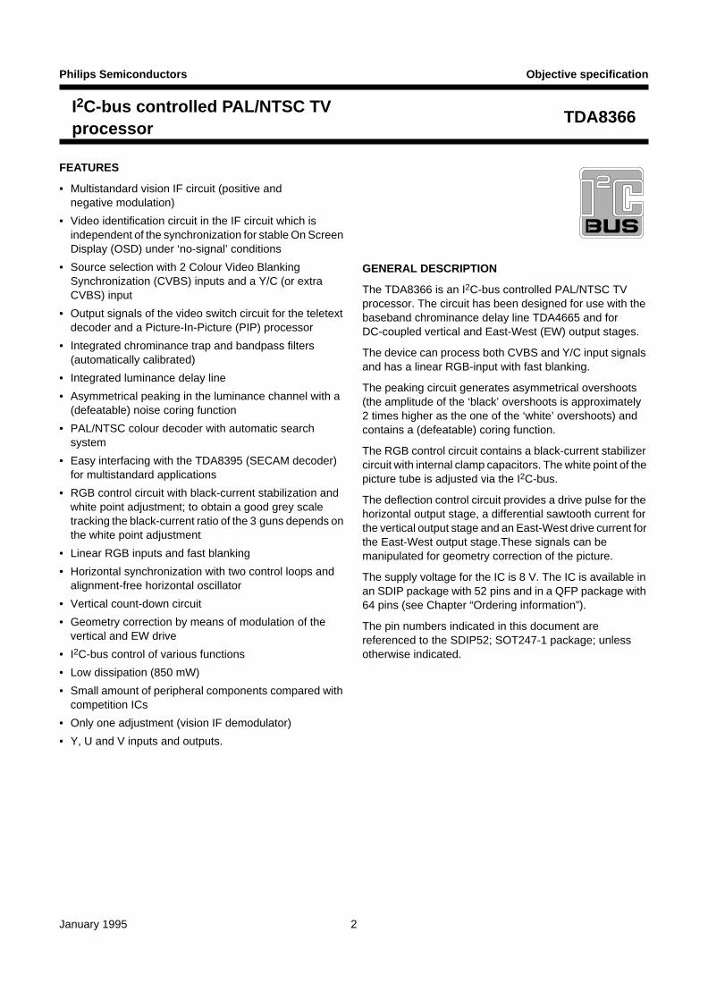
The TDA8366 is an I2C-bus controlled PAL/NTSC TVprocessor. The circuit has been designed for use with thebaseband chrominance delay line TDA4665 and forDC-coupled vertical and East-West (EW) output stages.
The device can process both CVBS and Y/C input signalsand has a linear RGB-input with fast blanking.
The peaking circuit generates asymmetrical overshoots(the amplitude of the ‘black’ overshoots is approximately2 times higher as the one of the ‘white’ overshoots) andcontains a (defeatable) coring function.
The RGB control circuit contains a black-current stabilizercircuit with internal clamp capacitors. The white point of thepicture tube is adjusted via the I2C-bus.
The deflection control circuit provides a drive pulse for thehorizontal output stage, a differential sawtooth current forthe vertical output stage and an East-West drive current forthe East-West output stage.These signals can bemanipulated for geometry correction of the picture.
The supply voltage for the IC is 8 V. The IC is available inan SDIP package with 52 pins and in a QFP package with64 pins (see Chapter “Ordering information”).
The pin numbers indicated in this document arereferenced to the SDIP52; SOT247-1 package; unlessotherwise indicated.

January 1995 3
Philips Semiconductors Objective specification
I2C-bus controlled PAL/NTSC TVprocessor
TDA8366
ORDERING INFORMATION
Note
1. When using IR reflow soldering it is recommended that the Drypack instructions in the “Quality Reference Handbook”(order number 9398 510 63011) are followed.
QUICK REFERENCE DATA
TYPE NUMBERPACKAGE
NAME DESCRIPTION VERSION
TDA8366 SDIP52 plastic shrink dual in-line package; 52 leads (600 mil) SOT247-1
TDA8366H QFP64(1) plastic quad flat package; 64 leads (lead length 1.95 mm);body 14 × 20 × 2.8 mm
SOT319-2
SYMBOL PARAMETER MIN. TYP. MAX. UNIT
Supply
VP supply voltage − 8.0 − V
IP supply current − 100 − mA
Input voltages
V46,47(rms) video IF amplifier sensitivity (RMS value) − 70 − µV
V15(p-p) external CVBS input (peak-to-peak value) − 1.0 − V
V9(p-p) S-VHS luminance input voltage (peak-to-peak value) − 1.0 − V
V8(p-p) S-VHS chroma input voltage (burst amplitude)(peak-to-peak value)
− 0.3 − V
V21,22,23(p-p) RGB inputs (peak-to-peak value) − 0.7 − V
Output signals
Vo(p-p) demodulated CVBS output (peak-to-peak value) − 2.5 − V
I52 tuner AGC output current range 0 − 5 mA
V36(p-p) TXT output voltage (peak-to-peak value) − 1.0 − V
V13(p-p) PIP output voltage (peak-to-peak value) − 1.0 − V
V28(p-p) −(R−Y) output voltage (peak-to-peak value) − 525 − mV
V27(p-p) −(B−Y) output voltage (peak-to-peak value) − 675 − mV
V26 Y output voltage − 450 − mV
V19,18,17(p-p) RGB output signal amplitudes (peak-to-peak value) − 2.0 − V
I38 horizontal output current 10 − − mA
I44,45 vertical output current 1 − − mA
I43 EW drive output current 0.5 − − mA
January 1995 4
Philips Semiconductors Objective specification
I2C-bus controlled PAL/NTSC TVprocessor
TDA8366
BLOCK DIAGRAM
handbook, full pagewidthM
LA74
5 -
1
AF
C A
ND
SA
MP
LE A
ND
HO
LD
IF A
MP
LIF
IER
AN
D D
EM
OD
ULA
TO
R
VID
EO
IDE
NT
IFIC
AT
ION
AG
C F
OR
IFA
ND
TU
NE
R
VID
EO
A
MP
LIF
IER
VID
EO
MU
TE
CV
BS
- S
WIT
CH
S-V
HS
- S
WIT
CH
BA
ND
PA
SS
TR
AP
SO
UN
DT
RA
P
52 51
CO
NT
RO
L D
AC
s17
x 6
bits
2 x
4 bi
ts
PA
L/N
TS
CD
EC
OD
ER
FIL
TE
RT
UN
ING
VE
RT
ICA
LS
YN
CS
EP
AR
AT
OR
SY
NC
SE
PA
RA
TO
RA
ND
1st
LO
OP
VC
O
AN
DC
ON
TR
OL
I C
-BU
ST
RA
NS
CE
IVE
R
2
3433
32
4.4
MH
z3.
6M
Hz
89
1336
1431
2nd
LOO
P A
ND
H
OR
IZO
NT
AL
OU
TP
UT
HO
RIZ
ON
TA
L/V
ER
TIC
AL
DIV
IDE
R
DE
LAY
AN
DP
EA
KIN
G
G-Y
MA
TR
IXA
ND
S
AT
CO
NT
RO
L
TD
A46
61
EW
GE
OM
ET
RY
VE
RT
ICA
LG
EO
ME
TR
Y
BLA
CK
CU
RR
EN
TS
TA
BIL
IZE
R
RG
B M
AT
RIX
AN
D
OU
TP
UT
RG
B IN
PU
TA
ND
S
WIT
CH
43
BR
IC
ON
TR
WH
ITE
P
OIN
T
19 18 17
V
(
8 V
)
2827
3029
2625
2122
2324
LUM
OU
T
LUM
IN
RI
GI
BI R
GB
INC
HR
OM
A CV
BS
/YPIP
O CV
BS
/TX
T
CV
BS
EX
T
DE
CD
ET X
TA
L2X
TA
L1
FT
DE
CD
IG
DE
CB
G
GN
D1
GN
D2
PH
1LF
CV
BS
IFV
OIN
T
411
15
AF
CID
EN
T
124647
IFIN
1
IFD
EM
2
IFD
EM
1
IFIN
2
PO
L
AG
CO
UT
(TU
NE
R)
SW
MU
TEP
OL
TO
P
SC
LS
DA
56
41
4212
73
1035
4039
3738HO
UT
SC
O
FB
IP
H2L
F
ref
ref
HU
ES
WS
AT
RO
GO
BO
20B
CLI
N
16B
LKIN
5049454448
EW
D
EH
TO
VD
R
VS
C
VD
R(n
eg)
(pos
)
SE
C
RY
OB
YO
BY
IR
YI
TD
A83
66
DE
CA
GC
ref
I ref
P1
V
(
8 V
)P
2
Fig
.1 B
lock
dia
gram
(S
DIP
52; S
OT
247-
1).
January 1995 5
Philips Semiconductors Objective specification
I2C-bus controlled PAL/NTSC TVprocessor
TDA8366
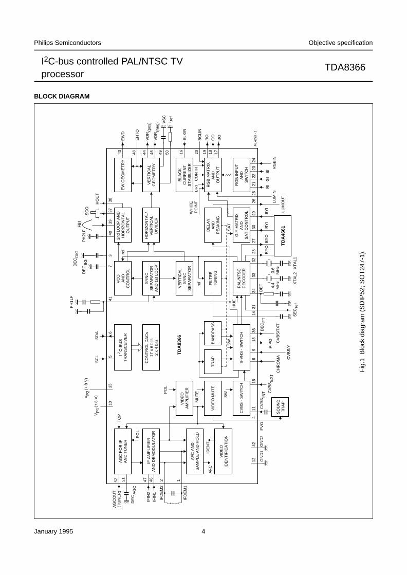
PINNING
SYMBOLPIN
DESCRIPTIONSDIP52 QFP64
IFDEM1 1 11 IF demodulator tuned circuit 1
IFDEM2 2 12 IF demodulator tuned circuit 2
DECDIG 3 13 decoupling digital supply
IFVO 4 14 IF video output
SCL 5 16 serial clock input
SDA 6 17 serial data input/output
DECBG 7 18 bandgap decoupling
CHROMA 8 20 chrominance input (S-VHS)
CVBS/Y 9 21 external CVBS/Y input
VP1 10 22 main supply voltage 1 (+8 V)
CVBSINT 11 29 internal CVBS input
GND1 12 25 ground 1
PIPO 13 27 picture-in-picture output
DECFT 14 28 decoupling filter tuning
CVBSEXT 15 24 external CVBS input
BLKIN 16 30 black-current input
BO 17 31 blue output
GO 18 32 green output
RO 19 33 red output
BCLIN 20 35 beam current limiter input
RI 21 37 red input for insertion
GI 22 38 green input for insertion
BI 23 39 blue input for insertion
RGBIN 24 40 RGB insertion input
LUMIN 25 42 luminance input
LUMOUT 26 43 luminance output
BYO 27 44 (B−Y) signal output
RYO 28 45 (R−Y) signal output
BYI 29 46 (B−Y) signal input
RYI 30 47 (R−Y) signal input
SECref 31 48 SECAM reference output
XTAL1 32 49 3.58 MHz crystal connection
XTAL2 33 50 4.43/3.58 MHz crystal connection
DET 34 52 loop filter phase detector
VP2 35 54 horizontal oscillator supply voltage (+8 V)
CVBS/TXT 36 55 CVBS/TXT output
SCO 37 56 sandcastle output
HOUT 38 57 horizontal output
January 1995 6
Philips Semiconductors Objective specification
I2C-bus controlled PAL/NTSC TVprocessor
TDA8366
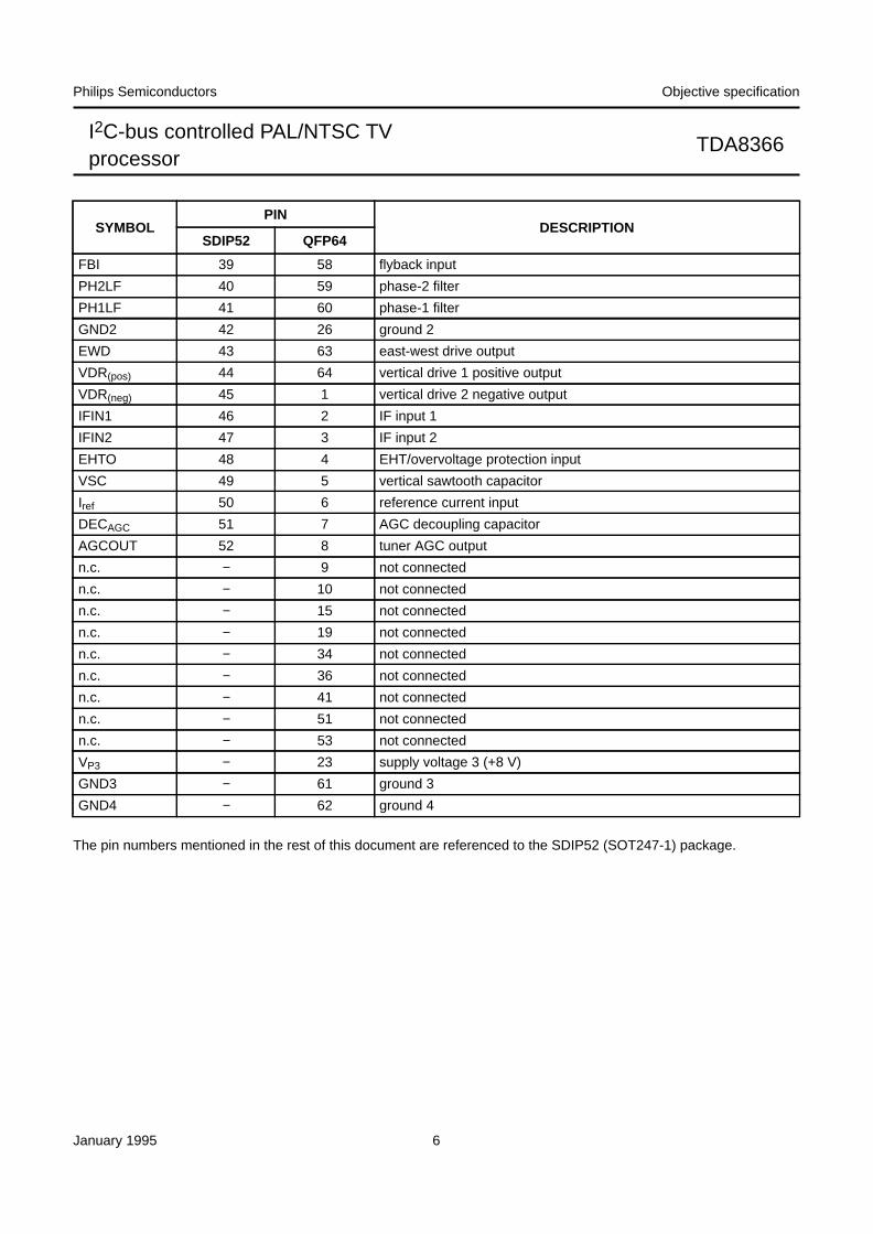
The pin numbers mentioned in the rest of this document are referenced to the SDIP52 (SOT247-1) package.
FBI 39 58 flyback input
PH2LF 40 59 phase-2 filter
PH1LF 41 60 phase-1 filter
GND2 42 26 ground 2
EWD 43 63 east-west drive output
VDR(pos) 44 64 vertical drive 1 positive output
VDR(neg) 45 1 vertical drive 2 negative output
IFIN1 46 2 IF input 1
IFIN2 47 3 IF input 2
EHTO 48 4 EHT/overvoltage protection input
VSC 49 5 vertical sawtooth capacitor
Iref 50 6 reference current input
DECAGC 51 7 AGC decoupling capacitor
AGCOUT 52 8 tuner AGC output
n.c. − 9 not connected
n.c. − 10 not connected
n.c. − 15 not connected
n.c. − 19 not connected
n.c. − 34 not connected
n.c. − 36 not connected
n.c. − 41 not connected
n.c. − 51 not connected
n.c. − 53 not connected
VP3 − 23 supply voltage 3 (+8 V)
GND3 − 61 ground 3
GND4 − 62 ground 4
SYMBOLPIN
DESCRIPTIONSDIP52 QFP64

January 1995 7
Philips Semiconductors Objective specification
I2C-bus controlled PAL/NTSC TVprocessor
TDA8366
handbook, halfpage1
2
3
4
5
6
7
8
9
10
11
12
13 40
39
38
37
36
35
34
33
32
31
30
29
28
27
14
15
16
17
18
19
20
22
23
24
25
26
21
42
41
43
44
45
46
47
48
49
50
51
52
MLA737 - 1
TDA8366
IFDEM1
IFDEM2
IFVO
SCL
SDA
DEC DIG
(neg)
(pos)CVBS/Y
VP1
GND1
CVBS EXT
CHROMA
BO
GO
RO
RGBIN
RI
GI
BI
LUMIN
LUMOUT
DEC FT
CVBS INT
BCLIN
DEC AGC
IFIN2
IFIN1
VDR
VDR
EWD
FBI
PH1LF
PH2LF
SCO
HOUT
CVBS/TXT
XTAL2
XTAL1
DET
BYO
RYO
RYI
BYI
DECBG
PIPO
BLKIN
SECref
VP2
GND2
AGCOUT
I ref
VSC
EHTO
Fig.2 Pin configuration (SDIP52).

January 1995 8
Philips Semiconductors Objective specification
I2C-bus controlled PAL/NTSC TVprocessor
TDA8366
Fig.3 Pin configuration (QFP64).
handbook, full pagewidth
1
2
3
4
5
6
7
8
9
10
11
12
13
14
15
16
17
18
19
51
50
49
47
46
45
44
43
42
41
40
39
38
37
36
35
34
33
48
20 21 22 24 25 26 27 28 29 30 31 3223
64 63 62 60 59 58 57 56 55 54 53 5261
TDA8366H
MLC756
IFDEM1
IFDEM2
IFVO
SCL
SDA
DEC DIG
CV
BS
/Y
VP
1
GN
D1
CV
BS
EX
T
CH
RO
MA
BO
GO
RO
RGBIN
RI
GI
BI
LUMIN
LUMOUT
DE
CF
T
CV
BS
INT
BCLIN
DECBG
PIP
O
BLK
IN
(neg)
(pos
)
DECAGC
IFIN2
IFIN1
VDR
VD
R
P2
VEW
D
FB
I
PH
1LF
GN
D3
GN
D4
PH
2LF
SC
O
HO
UT
CV
BS
/TX
T
XTAL2
XTAL1
DE
TBYO
RYO
RYI
BYI
SECref
VP
3
GN
D2
AGCOUT
I ref
VSC
EHTO
n.c.
n.c.
n.c.
n.c.
n.c.
n.c.
n.c.
n.c.
n.c.

January 1995 9
Philips Semiconductors Objective specification
I2C-bus controlled PAL/NTSC TVprocessor
TDA8366
FUNCTIONAL DESCRIPTION
Vision IF amplifier
The IF-amplifier contains 3 AC-coupled control stages witha total gain control range which is in excess of 66 dB. Thesensitivity of the circuit is comparable with that of modernIF-ICs. The reference carrier for the video demodulator isobtained by means of passive regeneration of the picturecarrier. The external reference tuned circuit is the onlyremaining adjustment of the IC.
The polarity of the demodulator can be switched via theI2C-bus in such a way that the circuit is suitable for bothpositive and negative modulated signals.
The AFC-circuit is driven with the same reference signal asthe video demodulator. To avoid that the video contentdisturbs the AFC operation a sample-and-hold circuit isapplied for signals with negative modulation. The capacitorfor this function is internal. The AFC information is suppliedto the tuning system via the I2C-bus.
The AGC-detector operates on top-sync or top white-leveldepending on the polarity of the demodulator. Thedemodulation polarity is switched via the I2C-bus. TheAGC detector time-constant capacitor is connectedexternally (this mainly because of the flexibility of theapplication). The time-constant of the AGC system duringpositive modulation is rather long to avoid visible variationsof the signal amplitude. To obtain an acceptable speed ofthe AGC system a circuit has been included which detectswhether the AGC detector is activated every frame period.When during 3 frame periods no action is detected thespeed of the system is increased.
The circuit contains a video identification circuit which isindependent of the synchronization circuit. Thereforesearch tuning is possible when the display section of thereceiver is used as a monitor. The identification output issupplied to the tuning system via the I2C-bus. Theinformation of this identification circuit can also be used toswitch the phase-1 (ϕ1) loop to a low gain when no signalis received so that a stable OSD display is obtained. Thecoupling of the video identification circuit with the ϕ1 loopcan be switched on and off via the I2C-bus.
Synchronization circuit
The sync separator is preceded by a controlled amplifierwhich adjusts the sync pulse amplitude to a fixed level.These pulses are fed to the slicing stage which is operatingat 50% of the amplitude.
The separated sync pulses are fed to the first phasedetector and to the coincidence detector. This coincidencedetector is only used to detect whether the line oscillator issynchronized and not for transmitter identification. The firstPhase-Locked Loop (PLL) has a very high-staticalsteepness so that the phase of the picture is independentof the line frequency.
The line oscillator is running at twice the line frequency.The oscillator capacitor is internal. Because of the spreadsof internal components an automatic adjustment circuithas been added to the IC. It compares the oscillatorfrequency with that of the crystal oscillator in the colourdecoder.
To protect the horizontal output transistor the horizontaldrive is switched-off when a power-on-reset is detected.The frequency of the oscillator is calibrated again when allsubaddress bytes have been sent. When the oscillator hasthe right frequency the calibration stops and the horizontaldrive is switched-on again via the soft start procedure(standby bit in normal mode). When the IC is switched-onthe same procedure is followed.
When the coincidence detector indicates an out-of-locksituation the calibration procedure is repeated.
The circuit has a second control loop to generate the drivepulses for the horizontal driver stage. During the start-upprocedure the duty cycle of the horizontal output pulseincreases from 0 to 50% in approximately 100 lines.
The vertical sawtooth generator drives the vertical outputand EW correction drive circuits. The geometry processingcircuits provide control of horizontal shift, EW width, EWparabola/width ratio, EW corner/parabola ratio, trapeziumcorrection, vertical shift, vertical slope, vertical amplitude,and the S-correction. All these controls can be set via theI2C-bus. The geometry processor has a differential current
January 1995 10
Philips Semiconductors Objective specification
I2C-bus controlled PAL/NTSC TVprocessor
TDA8366
output for the vertical drive signal and a single-endedoutput for the EW drive. Both the vertical drive and the EWdrive outputs can be modulated for EHT compensation.The EHT compensation pin is also used for overvoltageprotection.
The geometry processor also offers the possibilities forvertical compression (for display of 16 : 9 pictures on a4 : 3 screen) and vertical expansion (for display of4 : 3 pictures on a 16 : 9 screen with full picture width, orfor display of ‘letter-box’ transmissions on a 4 : 3 screenwith full picture height). For the expand mode it is possibleto shift the picture vertically (only one fixed position).
Also the de-interlace of the vertical output can be set viathe I2C-bus.
To avoid damage of the picture tube when the verticaldeflection fails the guard output current of the TDA8350can be supplied to the sandcastle output. When a failure isdetected the RGB-outputs are blanked and a bit is set(NDF) in the status byte of the I2C-bus. When no verticaldeflection output stage is connected this guard circuit willalso blank the output signals. This can be overruled bymeans of the EVG bit of subaddress 0A (see Table 1).
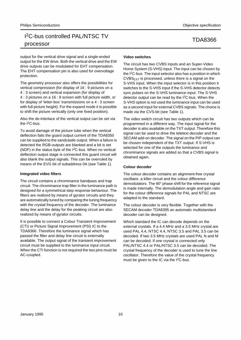
Integrated video filters
The circuit contains a chrominance bandpass and trapcircuit. The chrominance trap filter in the luminance path isdesigned for a symmetrical step response behaviour. Thefilters are realized by means of gyrator circuits and theyare automatically tuned by comparing the tuning frequencywith the crystal frequency of the decoder. The luminancedelay line and the delay for the peaking circuit are alsorealized by means of gyrator circuits.
It is possible to connect a Colour Transient Improvement(CTI) or Picture Signal Improvement (PSI) IC to theTDA8366. Therefore the luminance signal which haspassed the filter and delay line circuit is externallyavailable. The output signal of the transient improvementcircuit must be supplied to the luminance input circuit.When the CTI function is not required the two pins must beAC-coupled.
Video switches
The circuit has two CVBS inputs and an Super-VideoHome System (S-VHS) input. The input can be chosen bythe I2C-bus. The input selector also has a position in whichCVBSEXT is processed, unless there is a signal on theS-VHS input. When the input selector is in this position itswitches to the S-VHS input if the S-VHS detector detectssync pulses on the S-VHS luminance input. The S-VHSdetector output can be read by the I2C-bus. When theS-VHS option is not used the luminance input can be usedas a second input for external CVBS signals. The choice ismade via the CVS-bit (see Table 1).
The video switch circuit has two outputs which can beprogrammed in a different way. The input signal for thedecoder is also available on the TXT output. Therefore thissignal can be used to drive the teletext decoder and theSECAM add-on decoder. The signal on the PIP output canbe chosen independent of the TXT output. If S-VHS isselected for one of the outputs the luminance andchrominance signals are added so that a CVBS signal isobtained again.
Colour decoder
The colour decoder contains an alignment-free crystaloscillator, a killer circuit and the colour differencedemodulators. The 90° phase shift for the reference signalis made internally. The demodulation angle and gain ratiofor the colour difference signals for PAL and NTSC areadapted to the standard.
The colour decoder is very flexible. Together with theSECAM decoder TDA8395 an automatic multistandarddecoder can be designed.
Which standard the IC can decode depends on theexternal crystals. If a 4.4 MHz and a 3.5 MHz crystal areused PAL 4.4, NTSC 4.4, NTSC 3.5 and PAL 3.5 can bedecoded. If two 3.5 MHz crystals are used PAL N and Mcan be decoded. If one crystal is connected onlyPAL/NTSC 4.4 or PAL/NTSC 3.5 can be decoded. Thecrystal frequency of the decoder is used to tune the lineoscillator. Therefore the value of the crystal frequencymust be given to the IC via the I2C-bus.

January 1995 11
Philips Semiconductors Objective specification
I2C-bus controlled PAL/NTSC TVprocessor
TDA8366
RGB output circuit and black-current stabilization
The colour-difference signals are matrixed with theluminance signal to obtain the RGB-signals. For theRGB-inputs linear amplifiers have been chosen so that thecircuit is suited for signals coming from the SCARTconnector. The contrast and brightness control operate oninternal and external signals.
The output signal has an amplitude of approximately 2 Vblack-to-white at nominal input signals and nominalsettings of the controls.
The black current stabilization is realized by means of afeedback from the video output amplifiers to the RGBcontrol circuit. The ‘black current’ of the 3 guns of thepicture tube is internally measured and stabilized. Theblack level control is active during 4 lines at the end of thevertical blanking. During the first line the leakage current ismeasured and the following 3 lines the 3 guns areadjusted to the required level. The maximum acceptableleakage current is ±100 µA. The nominal value of the‘black current’ is 10 µA. The ratio of the currents for thevarious guns automatically tracks with the white pointadjustment so that the back-ground colour is the same asthe adjusted white point.
The input impedance of the ‘black-current’ measuring pinis 15 kΩ. Therefore the beam current during scan willcause the input voltage to exceed the supply voltage. Theinternal protection will start conducting so that theexcessive current is bypassed.
When the TV receiver is switched-on the black currentstabilization circuit is not active, the RGB outputs areblanked and beam current limiting input pin isshort-circuited. Only during the measuring lines will theoutputs supply a voltage of 5 V to the video output stageso that it can be detected if the picture tube is warming up.These pulses are switched-on after a waiting time ofapproximately 0.5 s. This ensures that the verticaldeflection is activated so that the measuring pulses are not
visible on the screen. As soon as the current supplied tothe measuring input exceeds a value of 190 µA thestabilization circuit is activated. After a waiting time ofapproximately 0.8 s the blanking and the beam currentlimiting input pin are released. The remaining switch-onbehaviour of the picture is determined by the external timeconstant of the beam current limiting network.
I2C-BUS SPECIFICATION
Valid subaddresses: 00 to 13; subaddress FE is reservedfor test purposes. Auto-increment mode is available forsubaddresses.
Start-up procedure
Read the status bytes until POR = 0 and send allsubaddress bytes. The horizontal output signal isswitched-on when the oscillator is calibrated. It is possibleto have the horizontal output signal available beforecalibration. Then the SFM bit must be set to logic 0.
Each time before the data in the IC is refreshed, the statusbytes must be read. If POR = 1, the procedure mentionedabove must be carried out to restart the IC.
When this procedure is not followed the horizontalfrequency may be incorrect after power-up or after apower dip.
handbook, halfpage
MLA743
A6 A5 A4 A3 A2 A1 A0
1 0 0 0 1 0 1 X
R/W
Fig.4 Slave address (8A).
X = don’t care.
January 1995 12
Philips Semiconductors Objective specification
I2C-bus controlled PAL/NTSC TVprocessor
TDA8366
Inputs
Table 1 Input status bits; note 1
Note
1. X = don’t care.
Table 2 Output status bits; note 1
Note
1. X = don’t care.
FUNCTIONSUBADDRESS
(HEX)
DATA BYTE
D7 D6 D5 D4 D3 D2 D1 D0
Source select 00 INA INB INC IND FOA FOB XA XB
Decoder mode 01 FORF FORS DL STB POC CM2 CM1 CM0
Hue 02 X X A5 A4 A3 A2 A1 A0
Horizontal shift (HS) 03 X X A5 A4 A3 A2 A1 A0
EW width (EW) 04 X X A5 A4 A3 A2 A1 A0
EW parabola/width (PW) 05 X X A5 A4 A3 A2 A1 A0
EW corner parabola (CP) 06 X X A5 A4 A3 A2 A1 A0
EW trapezium (TC) 07 X X A5 A4 A3 A2 A1 A0
Vertical slope (VS) 08 NCIN X A5 A4 A3 A2 A1 A0
Vertical amplitude (VA) 09 VID LBM A5 A4 A3 A2 A1 A0
S-correction (SC) 0A HCO EVG A5 A4 A3 A2 A1 A0
Vertical shift (VSH) 0B SBL PRD A5 A4 A3 A2 A1 A0
White point R 0C EXP CL A5 A4 A3 A2 A1 A0
White point G 0D SFM CVS A5 A4 A3 A2 A1 A0
White point B 0E MAT PHL A5 A4 A3 A2 A1 A0
Peaking 0F YD3 YD2 YD1 YD0 A3 A2 A1 A0
Brightness 10 RBL COR A5 A4 A3 A2 A1 A0
Saturation 11 IE1 X A5 A4 A3 A2 A1 A0
Contrast 12 AFW IFS A5 A4 A3 A2 A1 A0
AGC take-over 13 MOD VSW A5 A4 A3 A2 A1 A0
FUNCTIONSUBADDRESS
(HEX)
DATA BYTE
D7 D6 D5 D4 D3 D2 D1 D0
Output status bytes 00 POR FSI STS SL XPR CD2 CD1 CD0
01 NDF IN1 X IFI AFA AFB X X

January 1995 13
Philips Semiconductors Objective specification
I2C-bus controlled PAL/NTSC TVprocessor
TDA8366
INPUT CONTROL BITS
Table 3 Source select 1
Table 4 Source select 2
Table 5 Phase 1 (ϕ1) time constant
Note
1. X = don’t care.
Table 6 Crystal indication
INA INB DECODER AND TXT
0 0 CVBSINT
0 1 CVBSEXT
1 0 S-VHS
1 1 S-VHS (CVBSEXT)
INC IND PIP
0 0 CVBSINT
0 1 CVBSEXT
1 0 S-VHS
1 1 S-VHS (CVBSEXT)
FOA FOB (1) MODE
0 0 normal
0 1 slow
1 X fast
XA XB CRYSTAL
0 0 two 3.6 MHz
0 1 one 3.6 MHz (pin 32)
1 0 one 4.4 MHz (pin 33)
1 1 3.6 MHz (pin 32) and 4.4 MHz(pin 33)
Table 7 Forced field frequency
Note
1. When the forced mode is selected the divider will onlyswitch to that position when the horizontal oscillator isnot synchronized.
Table 8 Interlace
Table 9 Standby
Table 10 Synchronization mode
Table 11 Colour decoder mode
FORF FORS FIELD FREQUENCY
0 0 auto (60 Hz when line notsynchronized)
0 1 60 Hz; note 1
1 0 50 Hz; note 1
1 1 auto (50 Hz when line notsynchronized)
DL STATUS
0 interlace
1 de-interlace
STB MODE
0 standby
1 normal
POC MODE
0 active
1 not active
CM2 CM1 CM0 DECODER MODE
0 0 0 not forced, own intelligence
0 0 1 forced NTSC 3.6 MHz
0 1 0 forced PAL 4.4 MHz
0 1 1 forced SECAM
1 0 0 forced NTSC 4.4 MHz
1 0 1 forced PAL 3.6 MHz (pin 32)
1 1 0 forced PAL 3.6 MHz (pin 33)
1 1 1 no function

January 1995 14
Philips Semiconductors Objective specification
I2C-bus controlled PAL/NTSC TVprocessor
TDA8366
Table 12 Vertical divider mode
Table 13 Video ident mode
Table 14 Long blanking mode
Table 15 EHT tracking mode
Table 16 Enable vertical guard (RGB blanking)
Table 17 Service blanking
Table 18 Overvoltage input mode
Table 19 Vertical deflection mode
NCIN VERTICAL DIVIDER MODE
0 normal operation
1 switched to search window
VID VIDEO IDENT MODE
0 ϕ1 loop switched on and off
1 not active
LBM BLANKING MODE
0 adapted to standard (50 or 60 Hz)
1 fixed in accordance with 50 Hz standard
HCO TRACKING MODE
0 EHT tracking only on vertical
1 EHT tracking on vertical and EW
EVG VERTICAL GUARD MODE
0 not active
1 active
SBL SERVICE BLANKING MODE
0 off
1 on
PRD OVERVOLTAGE MODE
0 detection mode
1 protection mode
EXP CL VERTICAL DEFLECTION MODE
0 0 normal
0 1 compress
1 0 expand
1 1 expand and lift
Table 20 Horizontal frequency during switch-on
Table 21 Condition Y/C input
Table 22 PAL/NTSC matrix
Table 23 Colour crystal PLL
Table 24 Y-delay adjustment; note 1
Note
1. For an equal delay of the luminance and chrominancesignal the delay must be set at a value of 160 ns. Thisis only valid for a CVBS signal without groupdelay distortions.
Table 25 RGB blanking
Table 26 Noise coring (peaking)
SFM START-UP FREQUENCY
0 maximum
1 nominal
CVS Y-INPUT MODE
0 switched to Y/C mode
1 switched to CVBS mode
MAT MATRIX
0 adapted to standard
1 PAL
PHL STATE
0 PLL closed
1 oscillator free-running
YD0 to YD3 Y-DELAY
YD3 YD3 ∗ 160 ns +
YD2 YD2 ∗ 80 ns +
YD1 YD1 ∗ 40 ns +
YD0 YD0 ∗ 40 ns
RBL RGB BLANKING
0 not active
1 active
COR NOISE CORING
0 off
1 on

January 1995 15
Philips Semiconductors Objective specification
I2C-bus controlled PAL/NTSC TVprocessor
TDA8366
Table 27 Enable fast blanking
Table 28 AFC window
Table 29 IF sensitivity
Table 30 Modulation standard
Table 31 Video mute
OUTPUT CONTROL BITS
Table 32 Power-on-reset
Table 33 Field frequency indication
Table 34 S-VHS status
IE1 FAST BLANKING
0 not active
1 active
AFW AFC WINDOW
0 normal
1 enlarged
IFS IF SENSITIVITY
0 normal
1 reduced
MOD MODULATION
0 negative
1 positive
VSW STATE
0 normal operation
1 IF-video signal switched off
POR MODE
0 normal
1 power-down
FSI FREQUENCY
0 50 Hz
1 60 Hz
STS S-VHS INPUT
0 no signal
1 signal
Table 35 Phase 1 (ϕ1) lock indication
Table 36 X-ray protection
Table 37 Colour decoder mode
Table 38 Output vertical guard
Table 39 Indication RGB insertion
Table 40 Output video identification
SL INDICATION
0 not locked
1 locked
XPR OVERVOLTAGE
0 no overvoltage detected
1 overvoltage detected
CD2 CD1 CD0 STANDARD
0 0 0 no colour standard identified
0 0 1 NTSC 3.6 MHz
0 1 0 PAL 4.4 MHz
0 1 1 SECAM
1 0 0 NTSC 4.4 MHz
1 0 1 PAL 3.6 MHz (pin 32)
1 1 0 PAL 3.6 MHz (pin 33)
1 1 1 spare
NDF VERTICAL OUTPUT STAGE
0 OK
1 failure
IN1 RGB INSERTION
0 no (pin 24 LOW)
1 yes (pin 24 HIGH)
IFI VIDEO SIGNAL
0 no video signal identified
1 video signal identified
January 1995 16
Philips Semiconductors Objective specification
I2C-bus controlled PAL/NTSC TVprocessor
TDA8366
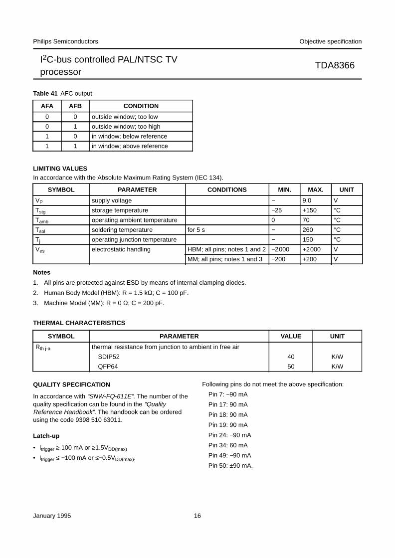
Table 41 AFC output
AFA AFB CONDITION
0 0 outside window; too low
0 1 outside window; too high
1 0 in window; below reference
1 1 in window; above reference
LIMITING VALUESIn accordance with the Absolute Maximum Rating System (IEC 134).
Notes
1. All pins are protected against ESD by means of internal clamping diodes.
2. Human Body Model (HBM): R = 1.5 kΩ; C = 100 pF.
3. Machine Model (MM): R = 0 Ω; C = 200 pF.
THERMAL CHARACTERISTICS
SYMBOL PARAMETER CONDITIONS MIN. MAX. UNIT
VP supply voltage − 9.0 V
Tstg storage temperature −25 +150 °CTamb operating ambient temperature 0 70 °CTsol soldering temperature for 5 s − 260 °CTj operating junction temperature − 150 °CVes electrostatic handling HBM; all pins; notes 1 and 2 −2000 +2000 V
MM; all pins; notes 1 and 3 −200 +200 V
SYMBOL PARAMETER VALUE UNIT
Rth j-a thermal resistance from junction to ambient in free air
SDIP52 40 K/W
QFP64 50 K/W
QUALITY SPECIFICATION
In accordance with “SNW-FQ-611E”. The number of thequality specification can be found in the “QualityReference Handbook”. The handbook can be orderedusing the code 9398 510 63011.
Latch-up
• Itrigger ≥ 100 mA or ≥1.5VDD(max)
• Itrigger ≤ −100 mA or ≤−0.5VDD(max).
Following pins do not meet the above specification:
Pin 7: −90 mA
Pin 17: 90 mA
Pin 18: 90 mA
Pin 19: 90 mA
Pin 24: −90 mA
Pin 34: 60 mA
Pin 49: −90 mA
Pin 50: ±90 mA.
January 1995 17
Philips Semiconductors Objective specification
I2C-bus controlled PAL/NTSC TVprocessor
TDA8366
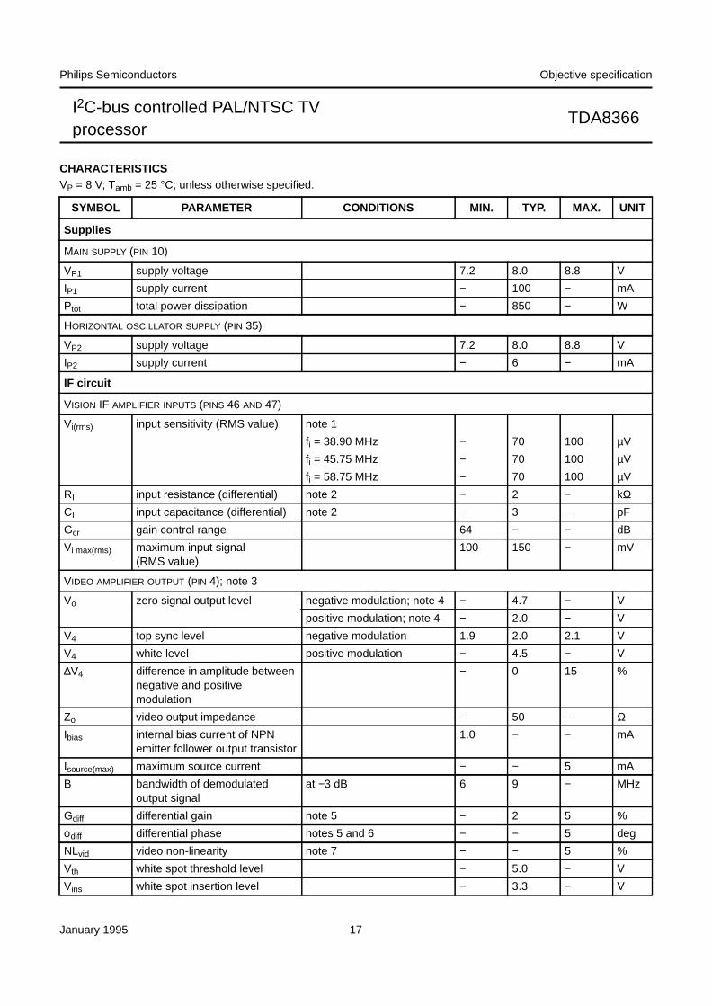
CHARACTERISTICSVP = 8 V; Tamb = 25 °C; unless otherwise specified.
SYMBOL PARAMETER CONDITIONS MIN. TYP. MAX. UNIT
Supplies
MAIN SUPPLY (PIN 10)
VP1 supply voltage 7.2 8.0 8.8 V
IP1 supply current − 100 − mA
Ptot total power dissipation − 850 − W
HORIZONTAL OSCILLATOR SUPPLY (PIN 35)
VP2 supply voltage 7.2 8.0 8.8 V
IP2 supply current − 6 − mA
IF circuit
VISION IF AMPLIFIER INPUTS (PINS 46 AND 47)
Vi(rms) input sensitivity (RMS value) note 1
fi = 38.90 MHz − 70 100 µV
fi = 45.75 MHz − 70 100 µV
fi = 58.75 MHz − 70 100 µV
RI input resistance (differential) note 2 − 2 − kΩCI input capacitance (differential) note 2 − 3 − pF
Gcr gain control range 64 − − dB
Vi max(rms) maximum input signal(RMS value)
100 150 − mV
VIDEO AMPLIFIER OUTPUT (PIN 4); note 3
Vo zero signal output level negative modulation; note 4 − 4.7 − V
positive modulation; note 4 − 2.0 − V
V4 top sync level negative modulation 1.9 2.0 2.1 V
V4 white level positive modulation − 4.5 − V
∆V4 difference in amplitude betweennegative and positivemodulation
− 0 15 %
Zo video output impedance − 50 − ΩIbias internal bias current of NPN
emitter follower output transistor1.0 − − mA
Isource(max) maximum source current − − 5 mA
B bandwidth of demodulatedoutput signal
at −3 dB 6 9 − MHz
Gdiff differential gain note 5 − 2 5 %
ϕdiff differential phase notes 5 and 6 − − 5 deg
NLvid video non-linearity note 7 − − 5 %
Vth white spot threshold level − 5.0 − V
Vins white spot insertion level − 3.3 − V
January 1995 18
Philips Semiconductors Objective specification
I2C-bus controlled PAL/NTSC TVprocessor
TDA8366
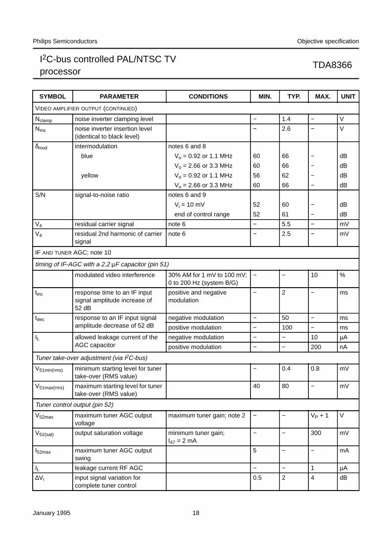
VIDEO AMPLIFIER OUTPUT (CONTINUED)
Nclamp noise inverter clamping level − 1.4 − V
Nins noise inverter insertion level(identical to black level)
− 2.6 − V
δmod intermodulation notes 6 and 8
blue Vo = 0.92 or 1.1 MHz 60 66 − dB
Vo = 2.66 or 3.3 MHz 60 66 − dB
yellow Vo = 0.92 or 1.1 MHz 56 62 − dB
Vo = 2.66 or 3.3 MHz 60 66 − dB
S/N signal-to-noise ratio notes 6 and 9
Vi = 10 mV 52 60 − dB
end of control range 52 61 − dB
V4 residual carrier signal note 6 − 5.5 − mV
V4 residual 2nd harmonic of carriersignal
note 6 − 2.5 − mV
IF AND TUNER AGC; note 10
timing of IF-AGC with a 2.2 µF capacitor (pin 51)
modulated video interference 30% AM for 1 mV to 100 mV;0 to 200 Hz (system B/G)
− − 10 %
tinc response time to an IF inputsignal amplitude increase of52 dB
positive and negativemodulation
− 2 − ms
tdec response to an IF input signalamplitude decrease of 52 dB
negative modulation − 50 − ms
positive modulation − 100 − ms
IL allowed leakage current of theAGC capacitor
negative modulation − − 10 µA
positive modulation − − 200 nA
Tuner take-over adjustment (via I2C-bus)
V51min(rms) minimum starting level for tunertake-over (RMS value)
− 0.4 0.8 mV
V51max(rms) maximum starting level for tunertake-over (RMS value)
40 80 − mV
Tuner control output (pin 52)
V52max maximum tuner AGC outputvoltage
maximum tuner gain; note 2 − − VP + 1 V
V52(sat) output saturation voltage minimum tuner gain;I47 = 2 mA
− − 300 mV
I52max maximum tuner AGC outputswing
5 − − mA
IL leakage current RF AGC − − 1 µA
∆Vi input signal variation forcomplete tuner control
0.5 2 4 dB
SYMBOL PARAMETER CONDITIONS MIN. TYP. MAX. UNIT

January 1995 19
Philips Semiconductors Objective specification
I2C-bus controlled PAL/NTSC TVprocessor
TDA8366
AFC OUTPUT (VIA I2C-BUS); note 11
RES AFC resolution − 2 − bits
Wsen window sensitivity 65 80 100 kHz
WsenL window sensitivity in largewindow mode
195 240 300 kHz
fos AFC offset note 6 − − 50 kHz
VIDEO IDENTIFICATION OUTPUT (VIA I2C-BUS)
td delay time of identification afterthe AGC has stabilized on anew transmitter
− − 10 ms
CVBS and S-VHS input switch
INTERNAL AND EXTERNAL CVBS INPUTS (PINS 11 AND 15)
V11(p-p) CVBS input voltage(peak-to-peak value)
note 12 − 1.0 1.4 V
I11 CVBS input current − 4 − µA
SSCVBS suppression of non-selectedCVBS input signal
notes 6 and 13 50 − − dB
S-VHS INPUT (PINS 8 AND 9)
V9(p-p) luminance input voltage(peak-to-peak value)
− 1.0 1.4 V
I9(p-p) luminance input current − 4 − µA
V8 chrominance input voltage(burst amplitude)
note 14 − 0.3 0.45 V
I8 chrominance input current − 4 − µA
TXT AND PIP OUTPUT SIGNALS (PINS 36 AND 13)
Vo(p-p) output signal amplitude(peak-to-peak value)
− 1.0 − V
Zo output impedance − − 250 ΩVTS top sync level − 2.5 − V
SYMBOL PARAMETER CONDITIONS MIN. TYP. MAX. UNIT
January 1995 20
Philips Semiconductors Objective specification
I2C-bus controlled PAL/NTSC TVprocessor
TDA8366
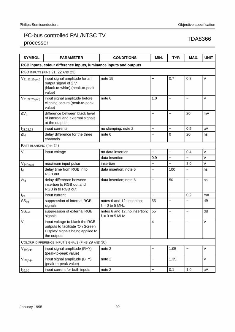
RGB inputs, colour difference inputs, luminance inputs and outputs
RGB INPUTS (PINS 21, 22 AND 23)
V21,22,23(p-p) input signal amplitude for anoutput signal of 2 V(black-to-white) (peak-to-peakvalue)
note 15 − 0.7 0.8 V
V21,22,23(p-p) input signal amplitude beforeclipping occurs (peak-to-peakvalue)
note 6 1.0 − − V
∆Vo difference between black levelof internal and external signalsat the outputs
− − 20 mV
I21,22,23 input currents no clamping; note 2 − − 0.5 µA
∆td delay difference for the threechannels
note 6 − 0 20 ns
FAST BLANKING (PIN 24)
Vi input voltage no data insertion − − 0.4 V
data insertion 0.9 − − V
V24(max) maximum input pulse insertion − − 3.0 V
td delay time from RGB in toRGB out
data insertion; note 6 − 100 − ns
∆td delay difference betweeninsertion to RGB out andRGB in to RGB out
data insertion; note 6 − 50 − ns
I24 input current − − 0.2 mA
SSint suppression of internal RGBsignals
notes 6 and 12; insertion;fi = 0 to 5 MHz
55 − − dB
SSext suppression of external RGBsignals
notes 6 and 12; no insertion;fi = 0 to 5 MHz
55 − − dB
VI input voltage to blank the RGBoutputs to facilitate ‘On ScreenDisplay’ signals being applied tothe outputs
4 − − V
COLOUR DIFFERENCE INPUT SIGNALS (PINS 29 AND 30)
V30(p-p) input signal amplitude (R−Y)(peak-to-peak value)
note 2 − 1.05 − V
V29(p-p) input signal amplitude (B−Y)(peak-to-peak value)
note 2 − 1.35 − V
I29,30 input current for both inputs note 2 − 0.1 1.0 µA
SYMBOL PARAMETER CONDITIONS MIN. TYP. MAX. UNIT

January 1995 21
Philips Semiconductors Objective specification
I2C-bus controlled PAL/NTSC TVprocessor
TDA8366
LUMINANCE INPUTS AND OUTPUTS (PINS 25 AND 26)
V26(p-p) output signal amplitude(peak-to-peak value)
top sync-white − 0.45 0.63 V
VTS top sync level − 2.5 − V
Zo output impedance − 250 − ΩV25(p-p) input signal amplitude
(peak-to-peak value)− 0.45 − V
Iclamp clamp current during burst key pulse − 200 − µA
Ii input current no clamp − − 0.5 µA
Chrominance filters
CHROMINANCE TRAP CIRCUIT
ftrap trap frequency − fosc − MHz
QF trap quality factor note 16 − 2 −SR colour subcarrier rejection 20 − − dB
CHROMINANCE BANDPASS CIRCUIT
fc centre frequency − fosc − MHz
QBP bandpass quality factor − 3 −
Delay line and peaking circuit
Y DELAY LINE
td delay time note 6 − 480 − ns
td1 tuning range delay time 8 steps −160 − +160 ns
B bandwidth of internal delay line note 6 5 − − MHz
PEAKING CONTROL; note 17
fc(p) peaking centre frequency − 3 − MHz
tW width of preshoot or overshoot note 2 − 160 − ns
OS overshoot positive − 20 − %
negative − 36 − %
peaking control curve 16 steps see Fig.5
CORING STAGE
S coring range − 15 − IRE
GW wave gain − 1.8 −
Horizontal synchronization circuits
SYNC VIDEO INPUT (PINS 9, 11 AND 15)
V9,11,15 sync pulse amplitude note 2 50 300 − mV
SLHS slicing level for horizontal sync note 18 − 50 − %
SLVS slicing level for vertical sync − 30 − %
SYMBOL PARAMETER CONDITIONS MIN. TYP. MAX. UNIT
negative half wave gainpositive half wave gain--------------------------------------------------------------

January 1995 22
Philips Semiconductors Objective specification
I2C-bus controlled PAL/NTSC TVprocessor
TDA8366
HORIZONTAL OSCILLATOR
ffr free running frequency − 15625 − Hz
∆ffr spread on free runningfrequency
− − ±2 %
∆f/∆VP frequency variation with respectto the supply voltage
VP = 8.0 V ±10%; note 6 − 0.2 0.5 %
∆f(max) frequency variation withtemperature
Tamb = 0 to 70 °C; note 6 − − 80 Hz
∆fosc(max) maximum frequency deviationat the start of the horizontaloutput
− − 75 %
FIRST CONTROL LOOP (FILTER CONNECTED TO PIN 41); note 19
fHR holding range PLL − ±0.9 ±1.2 kHz
fCR catching range PLL note 6 ±0.6 ±0.9 − kHz
S/N signal-to-noise ratio of the videoinput signal at which the timeconstant is switched
− 20 − dB
HYS hysteresis at the switching point − 1 − dB
SECOND CONTROL LOOP (CAPACITOR CONNECTED TO PIN 40)
∆ϕi/∆ϕo control sensitivity − 150 − µs/µs
tcr control range from start ofhorizontal output to flyback atnominal shift position
11 12 − µs
tshift horizontal shift range 63 steps ±2 − − µs
control sensitivity for dynamiccompensation
− 5.3 − µs/V
HORIZONTAL OUTPUT (PIN 38); note 20
VOL LOW level output voltage IO = 10 mA − − 0.3 V
IO(max) maximum allowed outputcurrent
10 − − mA
VO(max) maximum allowed outputvoltage
− − VP V
δ duty factor note 6 − 50 − %
FLYBACK PULSE INPUT (PIN 39)
VHSW switching level for horizontalblanking
− 0.4 − V
Vϕ2(SW) switching level for phase-2 loop − 4.0 − V
V39(max) maximum input voltage note 2 − 8.0 − V
Zi input impedance note 2 − 10 − MΩ
SYMBOL PARAMETER CONDITIONS MIN. TYP. MAX. UNIT
January 1995 23
Philips Semiconductors Objective specification
I2C-bus controlled PAL/NTSC TVprocessor
TDA8366
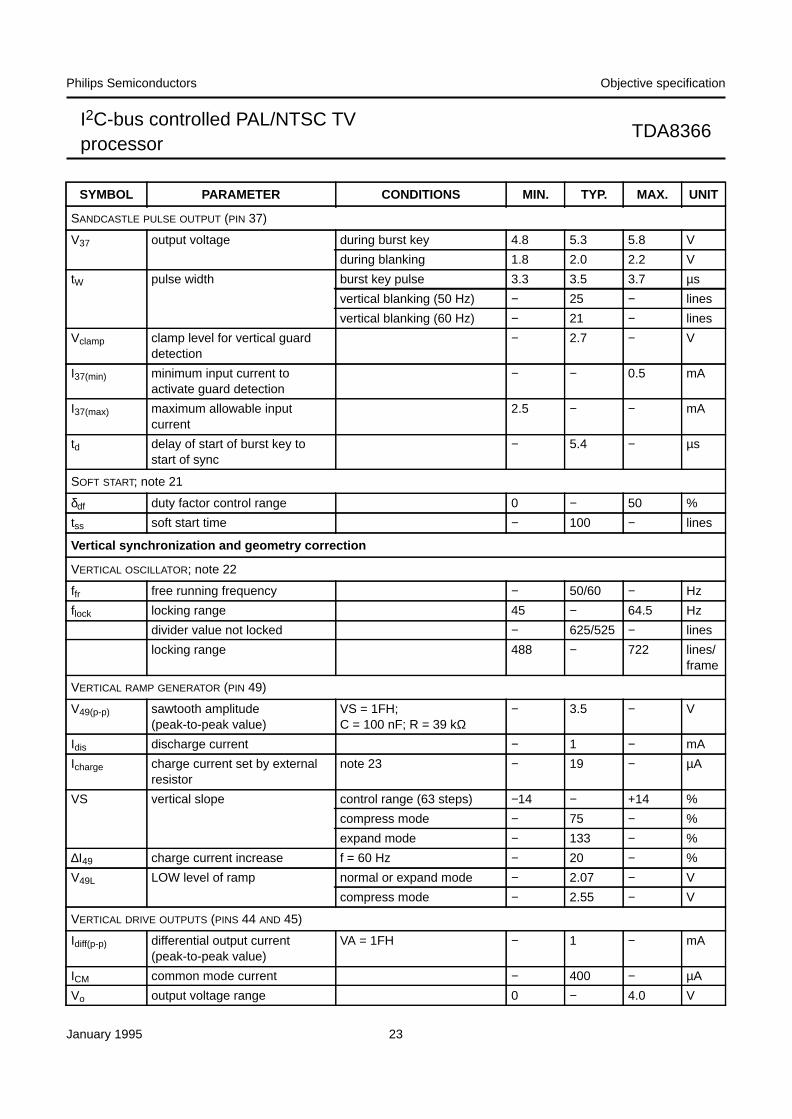
SANDCASTLE PULSE OUTPUT (PIN 37)
V37 output voltage during burst key 4.8 5.3 5.8 V
during blanking 1.8 2.0 2.2 V
tW pulse width burst key pulse 3.3 3.5 3.7 µs
vertical blanking (50 Hz) − 25 − lines
vertical blanking (60 Hz) − 21 − lines
Vclamp clamp level for vertical guarddetection
− 2.7 − V
I37(min) minimum input current toactivate guard detection
− − 0.5 mA
I37(max) maximum allowable inputcurrent
2.5 − − mA
td delay of start of burst key tostart of sync
− 5.4 − µs
SOFT START; note 21
δdf duty factor control range 0 − 50 %
tss soft start time − 100 − lines
Vertical synchronization and geometry correction
VERTICAL OSCILLATOR; note 22
ffr free running frequency − 50/60 − Hz
flock locking range 45 − 64.5 Hz
divider value not locked − 625/525 − lines
locking range 488 − 722 lines/frame
VERTICAL RAMP GENERATOR (PIN 49)
V49(p-p) sawtooth amplitude(peak-to-peak value)
VS = 1FH;C = 100 nF; R = 39 kΩ
− 3.5 − V
Idis discharge current − 1 − mA
Icharge charge current set by externalresistor
note 23 − 19 − µA
VS vertical slope control range (63 steps) −14 − +14 %
compress mode − 75 − %
expand mode − 133 − %
∆I49 charge current increase f = 60 Hz − 20 − %
V49L LOW level of ramp normal or expand mode − 2.07 − V
compress mode − 2.55 − V
VERTICAL DRIVE OUTPUTS (PINS 44 AND 45)
Idiff(p-p) differential output current(peak-to-peak value)
VA = 1FH − 1 − mA
ICM common mode current − 400 − µA
Vo output voltage range 0 − 4.0 V
SYMBOL PARAMETER CONDITIONS MIN. TYP. MAX. UNIT

January 1995 24
Philips Semiconductors Objective specification
I2C-bus controlled PAL/NTSC TVprocessor
TDA8366
EHT TRACKING/OVERVOLTAGE PROTECTION (PIN 48)
∆V48 input voltage 1.2 − 2.8 V
SMR scan modulation range −6 − +6 %
ϕvert vertical sensitivity − 7.5 − %/V
ϕEW EW sensitivity when switched-on − −7.5 − %/V
Ieq EW equivalent output current +120 − −120 µA
V48 overvoltage detection level − 3.9 − V
DE-INTERLACE
first field delay − 0.5H −
EW WIDTH
CR control range 63 steps 100 − 80 %
Ieq equivalent output current 0 − 400 µA
Vo EW output voltage range 1.0 − 8.0 V
Io EW output current range 0 − 900 µA
EW PARABOLA/WIDTH
CR control range 63 steps 0 − 24 %
Ieq equivalent output current EW = 3FH 0 − 480 µA
EW CORNER/PARABOLA
CR control range 63 steps −44 − 0 %
Ieq equivalent output current PW = 3FH; EW = 3FH −210 − 0 µA
EW TRAPEZIUM
CR control range 63 steps −4 − +4 %
Ieq equivalent output current −80 − +80 µA
VERTICAL AMPLITUDE
CR control range 63 steps; SC = 00H 80 − 120 %
63 steps; SC = 3FH 86 − 112 %
Ieqdiff(p-p) equivalent differential verticaldrive output current(peak-to-peak value)
SC = 00H 800 − 1200 µA
VERTICAL SHIFT
CR control range 63 steps −4 − +4 %
Ieqdiff(p-p) equivalent differential verticaldrive output current(peak-to-peak value)
−40 − +40 µA
S-CORRECTION
CR control range 63 steps 0 − 25 %
SYMBOL PARAMETER CONDITIONS MIN. TYP. MAX. UNIT

January 1995 25
Philips Semiconductors Objective specification
I2C-bus controlled PAL/NTSC TVprocessor
TDA8366
Colour demodulation part
CHROMINANCE AMPLIFIER
ACCcr ACC control range note 24 26 − − dB
∆V change in amplitude of theoutput signals over the ACCrange
− − 2 dB
THRon threshold colour killer ON −23 −26 −29 dB
HYSoff hysteresis colour killer OFF strong signal conditions;S/N ≥ 40 dB; note 6
− +3 − dB
noisy input signals; note 6 − +1 − dB
ACL CIRCUIT
chrominance burst ratio atwhich the ACL starts to operate
2.3 − 2.7
REFERENCE PART
Phase-locked loop; note 25
fCR catching range 300 500 − Hz
∆ϕ phase shift for a ±400 Hzdeviation of the oscillatorfrequency
note 6 − − 2 deg
Oscillator
TCosc temperature coefficient of theoscillator frequency
note 6 − 2.0 2.5 Hz/K
∆fosc oscillator frequency deviationwith respect to the supply
note 6; VP = 8 V ±10% − − 250 Hz
Ri input resistance pin 32; f = 3.58 MHz; note 2 − 1.5 − kΩpin 33; f = 4.43 MHz; note 2 − 1.0 − kΩ
Ci input capacitance pins 32 and 33; note 2 − − 10 pF
HUE CONTROL
HUEcr hue control range 63 steps; see Fig.6 ±35 ±40 − deg
∆HUE hue variation for ±10% VP note 6 − 0 − deg
∆HUE/∆T hue variation with temperature Tamb = 0 to 70 °C; note 6 − 0 − deg
SYMBOL PARAMETER CONDITIONS MIN. TYP. MAX. UNIT

January 1995 26
Philips Semiconductors Objective specification
I2C-bus controlled PAL/NTSC TVprocessor
TDA8366
DEMODULATORS (PINS 27 AND 28)
V28(p-p) (R−Y) output signal amplitude(peak-to-peak value)
note 26 − 0.525 − V
V27(p-p) (B−Y) output signal amplitude(peak-to-peak value)
note 26 − 0.675 − V
G gain between bothdemodulators G(B−Y) andG(R−Y)
1.60 1.78 1.96
∆V spread of signal amplitude ratioPAL/NTSC
note 6 −1 − +1 dB
Zo output impedance (R−Y)/(B−Y)output
note 6 − 500 − Ω
B bandwidth of demodulators −3 dB; note 27 − 650 − kHz
V27,28(p-p) residual carrier output(peak-to-peak value)
f = fosc; (R−Y) output 5 mV
f = fosc; (B−Y) output − − 5 mV
f = 2fosc; (R−Y) output 5 mV
f = 2fosc; (B−Y) output − − 5 mV
V28(p-p) H/2 ripple at (R−Y) output(peak-to-peak value)
− − 25 mV
∆Vo/∆T change of output signalamplitude with temperature
note 6 − 0.1 − %/K
∆Vo/∆VP change of output signalamplitude with supply voltage
note 6 − − ±0.1 dB
ϕe phase error in the demodulatedsignals
− − ±5 deg
COLOUR DIFFERENCE MATRICES IN CONTROL CIRCUIT
PAL or (SECAM mode with TDA8395); (R−Y) and (B−Y) not affected
(G−Y)/(R−Y) ratio of demodulated signals − −0.51±10%
−
(G−Y)/(B−Y) ratio of demodulated signals − −0.19±25%
−
NTSC mode; the colour-difference matrix results in the following signals (nominal hue setting)
(B−Y) (B−Y) signal (B−Y)
(R−Y) (R−Y) signal 1.39(R−Y) − 0.07(B−Y)
(G−Y) (G−Y) signal −0.46(R−Y) − 0.15(B−Y)
SYMBOL PARAMETER CONDITIONS MIN. TYP. MAX. UNIT
January 1995 27
Philips Semiconductors Objective specification
I2C-bus controlled PAL/NTSC TVprocessor
TDA8366
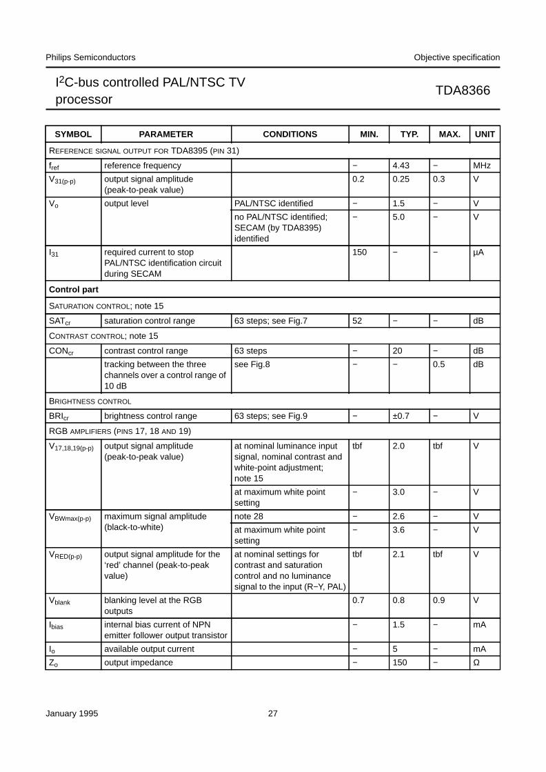
REFERENCE SIGNAL OUTPUT FOR TDA8395 (PIN 31)
fref reference frequency − 4.43 − MHz
V31(p-p) output signal amplitude(peak-to-peak value)
0.2 0.25 0.3 V
Vo output level PAL/NTSC identified − 1.5 − V
no PAL/NTSC identified;SECAM (by TDA8395)identified
− 5.0 − V
I31 required current to stopPAL/NTSC identification circuitduring SECAM
150 − − µA
Control part
SATURATION CONTROL; note 15
SATcr saturation control range 63 steps; see Fig.7 52 − − dB
CONTRAST CONTROL; note 15
CONcr contrast control range 63 steps − 20 − dB
tracking between the threechannels over a control range of10 dB
see Fig.8 − − 0.5 dB
BRIGHTNESS CONTROL
BRIcr brightness control range 63 steps; see Fig.9 − ±0.7 − V
RGB AMPLIFIERS (PINS 17, 18 AND 19)
V17,18,19(p-p) output signal amplitude(peak-to-peak value)
at nominal luminance inputsignal, nominal contrast andwhite-point adjustment;note 15
tbf 2.0 tbf V
at maximum white pointsetting
− 3.0 − V
VBWmax(p-p) maximum signal amplitude(black-to-white)
note 28 − 2.6 − V
at maximum white pointsetting
− 3.6 − V
VRED(p-p) output signal amplitude for the‘red’ channel (peak-to-peakvalue)
at nominal settings forcontrast and saturationcontrol and no luminancesignal to the input (R−Y, PAL)
tbf 2.1 tbf V
Vblank blanking level at the RGBoutputs
0.7 0.8 0.9 V
Ibias internal bias current of NPNemitter follower output transistor
− 1.5 − mA
Io available output current − 5 − mA
Zo output impedance − 150 − Ω
SYMBOL PARAMETER CONDITIONS MIN. TYP. MAX. UNIT
January 1995 28
Philips Semiconductors Objective specification
I2C-bus controlled PAL/NTSC TVprocessor
TDA8366
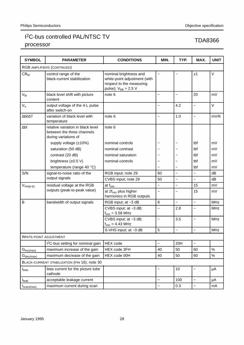
RGB AMPLIFIERS (CONTINUED)
CRbl control range of theblack-current stabilization
nominal brightness andwhite-point adjustment (withrespect to the measuringpulse); Vblk = 2.5 V
− − ±1 V
Vbl black level shift with picturecontent
note 6 − − 20 mV
Vo output voltage of the 4-L pulseafter switch-on
− 4.2 − V
∆bl/∆T variation of black level withtemperature
note 6 − 1.0 − mV/K
∆bl relative variation in black levelbetween the three channelsduring variations of
note 6
supply voltage (±10%) nominal controls − − tbf mV
saturation (50 dB) nominal contrast − − tbf mV
contrast (20 dB) nominal saturation − − tbf mV
brightness (±0.5 V) nominal controls − − tbf mV
temperature (range 40 °C) − − tbf mV
S/N signal-to-noise ratio of theoutput signals
RGB input; note 29 60 − − dB
CVBS input; note 29 50 − − dB
Vres(p-p) residual voltage at the RGBoutputs (peak-to-peak value)
at fosc − − 15 mV
at 2fosc plus higherharmonics in RGB outputs
− − 15 mV
B bandwidth of output signals RGB input; at −3 dB 8 − − MHz
CVBS input; at −3 dB;fosc = 3.58 MHz
− 2.8 − MHz
CVBS input; at −3 dB;fosc = 4.43 MHz
− 3.5 − MHz
S-VHS input; at −3 dB 5 − − MHz
WHITE-POINT ADJUSTMENT
I2C-bus setting for nominal gain HEX code − 20H −Ginc(max) maximum increase of the gain HEX code 3FH 40 50 60 %
Gdec(max) maximum decrease of the gain HEX code 00H 40 50 60 %
BLACK-CURRENT STABILIZATION (PIN 16); note 30
Ibias bias current for the picture tubecathode
− 10 − µA
Ileak acceptable leakage current − 100 − µA
Iscan(max) maximum current during scan − 0.3 − mA
SYMBOL PARAMETER CONDITIONS MIN. TYP. MAX. UNIT
January 1995 29
Philips Semiconductors Objective specification
I2C-bus controlled PAL/NTSC TVprocessor
TDA8366
Notes
1. On set AGC.
2. This parameter is not tested during production and is just given as application information for the designer of thetelevision receiver.
3. Measured at 10 mV (RMS) top sync input signal.
4. So called projected zero point, i.e. with switched demodulator.
5. Measured in accordance with the test line given in Fig.10. For the differential phase test the peak white setting isreduced to 87%.
a) The differential gain is expressed as a percentage of the difference in peak amplitudes between the largest andsmallest value relative to the subcarrier amplitude at blanking level.
b) The phase difference is defined as the difference in degrees between the largest and smallest phase angle.
6. This parameter is not tested during production but is guaranteed by the design and qualified by means of matrixbatches which are made in the pilot production period.
7. This figure is valid for the complete video signal amplitude (peak white-to-black), see Fig.11.
8. The test set-up and input conditions are given in Fig.12. The figures are measured with an input signal of10 mV RMS.
9. Measured with a source impedance of 75 Ω, where:
10. To obtain a good noise immunity of the AGC circuit the AGC detector is gated during the sync pulse. This gating isswitched-off during the vertical retrace to avoid disturbances of the signal amplitude due to phase errors of theincoming video signal which are caused by the head-switching of VCRs.
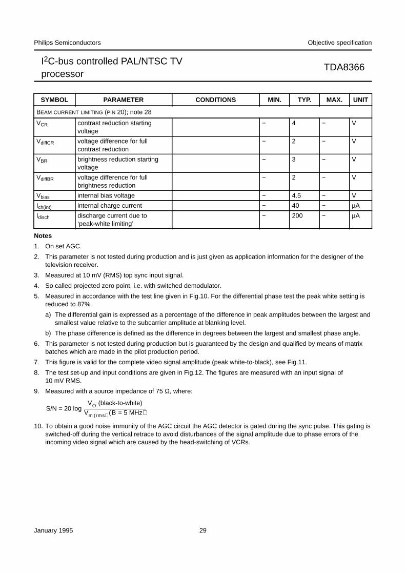
BEAM CURRENT LIMITING (PIN 20); note 28
VCR contrast reduction startingvoltage
− 4 − V
VdiffCR voltage difference for fullcontrast reduction
− 2 − V
VBR brightness reduction startingvoltage
− 3 − V
VdiffBR voltage difference for fullbrightness reduction
− 2 − V
Vbias internal bias voltage − 4.5 − V
Ich(int) internal charge current − 40 − µA
Idisch discharge current due to‘peak-white limiting’
− 200 − µA
SYMBOL PARAMETER CONDITIONS MIN. TYP. MAX. UNIT
S/N = 20 logVO (black-to-white)
Vm rms( ) B = 5 MHz( )---------------------------------------------------------
January 1995 30
Philips Semiconductors Objective specification
I2C-bus controlled PAL/NTSC TVprocessor
TDA8366
11. The AFC slope is directly related to the Q-factor of the demodulator tuned circuit. The given AFC steepness isobtained with a Q-factor of 60. The AFC off-set is tested with a double sideband input signal and with the referencetuned circuit tuned to minimum AGC voltage (optimum tuning for the demodulator).
The tuning information is supplied to the tuning system via the I2C-bus. Two bits have been reserved for this function.The first bit indicates whether the tuning is within the given window. The second bit indicates the direction of thetuning. Bit indications:
a) AFA = 1; tuning inside window.
b) AFA = 0; tuning outside window.
c) AFB = 1; tuning too high.
d) AFB = 0; tuning too low.
To improve the speed of search tuning systems the AFC window can be increased to about 240 kHz. The width ofthe window can be set by means of the AFW bit in subaddress 03.
12. Signal with negative-going sync. Amplitude includes sync pulse amplitude.
13. This parameter is measured at nominal settings of the various controls.
14. Indicated is a signal for a colour bar with 75% saturation (chroma : burst ratio = 2.2 : 1).
15. Nominal contrast is specified with the DAC in position 20H. Nominal saturation as maximum −10 dB. In the nominalbrightness setting the black level at the outputs is identical to the level of the black-current measuring pulses.
16. The −3 dB bandwidth of the circuit can be calculated by means of the following equation:
17. Valid for a signal amplitude on the Y-input of 0.7 V black-to-white (100 IRE) with a rise time (10% to 90%) of 70 nsand the video switch in the Y/C mode. During production the peaking function is not tested by measuring theovershoots but by measuring the frequency response of the Y output.
18. The slicing level is independent of sync pulse amplitude. The given percentage is the distance between the slicinglevel and the black level (back porch).
19. To obtain a good performance for both weak signal and VCR playback the time constant of the first control loop isswitched depending on the input signal condition and the condition of the I2C-bus. Therefore the circuit contains anoise detector and the time constant is switched to ‘slow’ when too much noise is present in the signal. In the ‘fast’mode during the vertical retrace time the phase detector current is increased 50% so that phase errors due tohead-switching of the VCR are corrected as soon as possible. Switching between the two modes can beautomatically or overruled by the I2C-bus.
The circuit contains a video identification circuit which is independent of first loop. This identification circuit can beused to close or open the first control loop when a video signal is present or not present on the input. This enablesa stable On Screen Display (OSD) when just noise is present at the input. The coupling of the video identificationcircuit with the first loop can be defeated via the I2C-bus.
When the horizontal PLL is set to the ‘slow’ mode (via I2C-bus bits FOA and FOB) or during weak signal conditionsin the ‘automatic’ mode the phase detector is gated to obtain a good noise immunity. The width of the gating pulseis 5.7 µs.
The output current of the phase detector in the various conditions are shown in Table 42.
20. During the start-up period of the oscillator the duty factor of the output pulse rises gradually from 0% to 50% (timeapproximately 100 lines).
21. The start-up frequency depends on the SFM bit in the I2C-bus protocol. When SFM = 0 the frequency starts at a high(non calibrated) value. When SFM = 1 the output signal will only be available after calibration.
f 3 dB– fosc 1 12Q--------–
=
January 1995 31
Philips Semiconductors Objective specification
I2C-bus controlled PAL/NTSC TVprocessor
TDA8366
22. The timing pulses for the vertical ramp generator are obtained from the horizontal oscillator via a divider circuit. Thisdivider circuit has 3 modes of operation:
a) Search mode ‘large window’.
This mode is switched on when the circuit is not synchronized or when a non-standard signal (number of lines perframe in the 50 Hz mode is between 311 and 314 and in the 60 Hz mode between 261 and 264). In the search modethe divider can be triggered between line 244 and line 361 (approximately 45 to 64.5 Hz).
b) Standard mode ‘narrow window’.
This mode is switched on when more than 15 succeeding vertical sync pulses are detected in the narrow window.When the circuit is in the standard mode and a vertical sync pulse is missing the retrace of the vertical ramp generatoris started at the end of the window. Consequently, the disturbance of the picture is very small. The circuit will switchback to the search window when, for 6 successive vertical periods, no sync pulses are found within the window.
c) Standard TV-norm (divider ratio 525 (60 Hz) or 625 (50 Hz).
When the system is switched to the narrow window it is checked whether the incoming vertical sync pulses are inaccordance with the TV-norm. When 15 standard TV-norm pulses are counted the divider system is switched to thestandard divider ratio mode. In this mode the divider is always reset at the standard value even if the vertical syncpulse is missing.
When 3 vertical sync pulses are missed the system switches back to the narrow window and when also in thiswindow no sync pulses are found (condition 3 missing pulses) the system switches over to the search window.
The vertical divider needs some waiting time during channel-switching of the tuner. When a fast reaction of thedivider is required during channel-switching the system can be forced to the search window by means of the NCIN bitin subaddress 08.
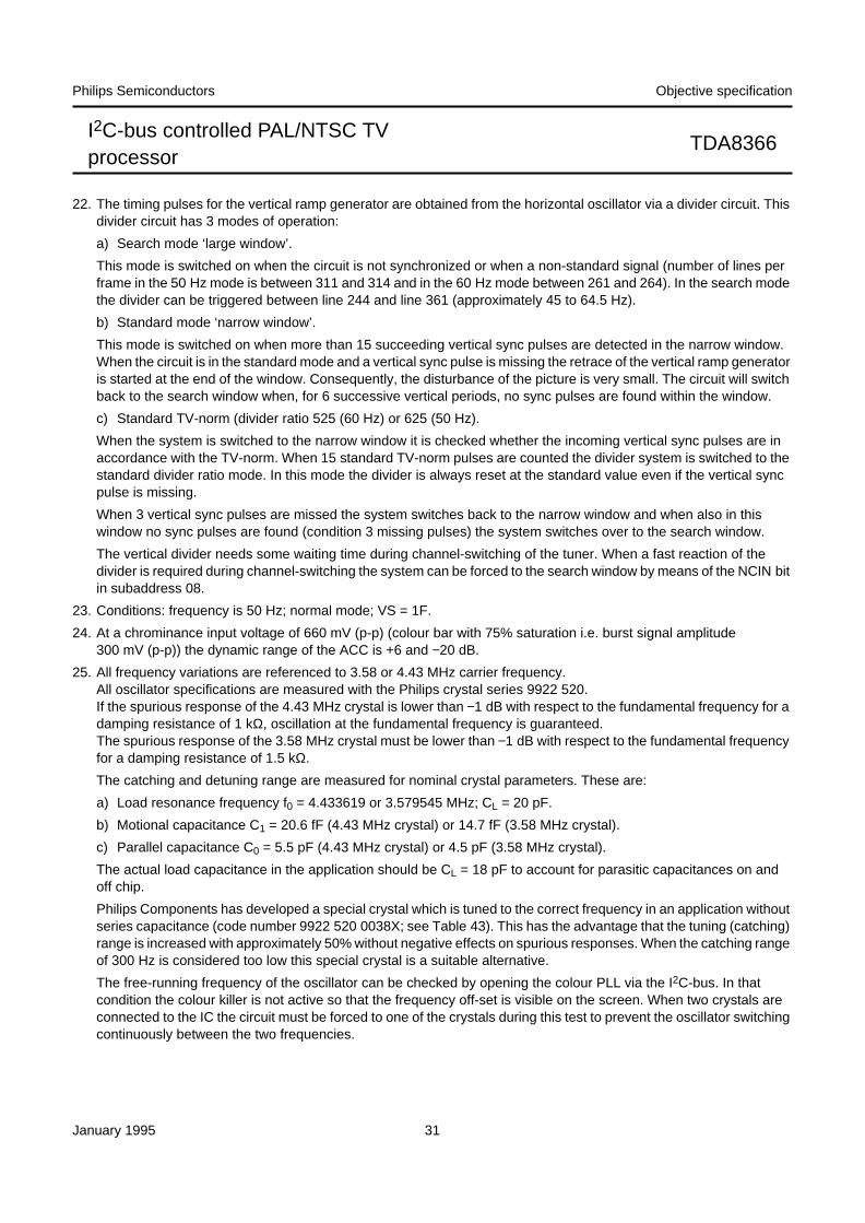
23. Conditions: frequency is 50 Hz; normal mode; VS = 1F.
24. At a chrominance input voltage of 660 mV (p-p) (colour bar with 75% saturation i.e. burst signal amplitude300 mV (p-p)) the dynamic range of the ACC is +6 and −20 dB.
25. All frequency variations are referenced to 3.58 or 4.43 MHz carrier frequency.All oscillator specifications are measured with the Philips crystal series 9922 520.If the spurious response of the 4.43 MHz crystal is lower than −1 dB with respect to the fundamental frequency for adamping resistance of 1 kΩ, oscillation at the fundamental frequency is guaranteed.The spurious response of the 3.58 MHz crystal must be lower than −1 dB with respect to the fundamental frequencyfor a damping resistance of 1.5 kΩ.
The catching and detuning range are measured for nominal crystal parameters. These are:
a) Load resonance frequency f0 = 4.433619 or 3.579545 MHz; CL = 20 pF.
b) Motional capacitance C1 = 20.6 fF (4.43 MHz crystal) or 14.7 fF (3.58 MHz crystal).
c) Parallel capacitance C0 = 5.5 pF (4.43 MHz crystal) or 4.5 pF (3.58 MHz crystal).
The actual load capacitance in the application should be CL = 18 pF to account for parasitic capacitances on andoff chip.
Philips Components has developed a special crystal which is tuned to the correct frequency in an application withoutseries capacitance (code number 9922 520 0038X; see Table 43). This has the advantage that the tuning (catching)range is increased with approximately 50% without negative effects on spurious responses. When the catching rangeof 300 Hz is considered too low this special crystal is a suitable alternative.
The free-running frequency of the oscillator can be checked by opening the colour PLL via the I2C-bus. In thatcondition the colour killer is not active so that the frequency off-set is visible on the screen. When two crystals areconnected to the IC the circuit must be forced to one of the crystals during this test to prevent the oscillator switchingcontinuously between the two frequencies.

January 1995 32
Philips Semiconductors Objective specification
I2C-bus controlled PAL/NTSC TVprocessor
TDA8366
26. The (R−Y) and (B−Y) signals are demodulated with a phase difference of the reference carrier of 90° and a gain ratio
. The matrixing to the required signals is achieved in the control part.
27. This parameter indicates the bandwidth of the complete chrominance circuit including the chrominance bandpassfilter. The bandwidth of the low-pass filter of the demodulator is approximately 1 MHz.
28. At nominal setting of the gain control. When this amplitude is exceeded the peak-white limiting circuit will reduce thecontrast. The control voltage is generated via the external capacitor connected to the beam-current limiting input.
29. Signal-to-noise ratio (S/N) is specified as peak-to-peak signal with respect to RMS noise (bandwidth 5 MHz).
30. This is a current input. The indicated value of the nominal bias current is obtained at the nominal setting of the gain(white point) control. The actual value of the bias current depends on the gain control setting of each channel. As aresult the ‘black-current’ of each gun is adapted to the white point setting so that the back-ground colour will followthe white point adjustment.
Table 42 Output current of the phase detector in the various conditions
I2C-BUS COMMANDS IC CONDITIONS ϕ-1 CURRENT/MODE
VID POC FOA FOB IDENT COIN NOISE SCAN V-RETR GATING MODE
− 0 0 0 yes yes yes 30 30 yes auto
− 0 0 0 yes no − 180 270 no auto
− 0 0 1 yes yes − 30 30 yes slow
− 0 0 1 yes no − 180 270 no slow
− 0 1 − yes − − 180 270 no fast
0 0 − − no − − 6 6 no OSD
− 1 − − − − − − − − off
B Y–( )R Y–( )--------------------- 1.78=
Table 43 Code numbers for special crystals
SYSTEMFREQUENCY
(MHz)CODE NUMBER
PAL-N 3.582056 9922 520 00381
NTSC-M 3.579545 9922 520 00382
PAL-M 3.575611 9922 520 00383
PAL-B/G 4.433619 9922 520 00384
January 1995 33
Philips Semiconductors Objective specification
I2C-bus controlled PAL/NTSC TVprocessor
TDA8366
MLA738 - 150
30
10
10
30
50
(%)
0 4 8 C 10FDAC (HEX)
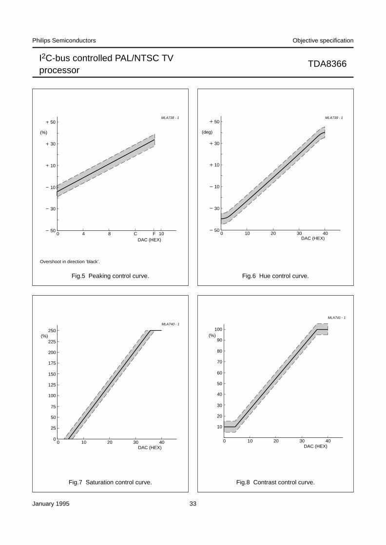
Fig.5 Peaking control curve.
Overshoot in direction ‘black’.
MLA739 - 150
30
10
10
30
50
(deg)
0 10 20 30 40DAC (HEX)
Fig.6 Hue control curve.
MLA740 - 1
250
25
0
(%)
0 10 20 30 40DAC (HEX)
50
75
100
125
150
175
200
225
Fig.7 Saturation control curve. Fig.8 Contrast control curve.
MLA741 - 1
90
50
10
(%)
0 10 20 30 40DAC (HEX)
20
30
40
60
70
80
100

January 1995 34
Philips Semiconductors Objective specification
I2C-bus controlled PAL/NTSC TVprocessor
TDA8366
MLA742 - 1
0.7
0.35
0
0.35
0.7
0
(V)
0 10 20 30 40DAC (HEX)
Fig.9 Brightness control curve.
Relative variation with respect to the measuring pulse.
MBC212
100%92%
30%
16 %
for negative modulation 100% = 10% rest carrier
Fig.10 Video output signal.
MBC211
100%
86%
72%
58%
44%
30%
646056524844403632221210 26 µs
Fig.11 Test signal waveform.

January 1995 35
Philips Semiconductors Objective specification
I2C-bus controlled PAL/NTSC TVprocessor
TDA8366
MBC213SC CC PC
30 dB
13.2 dB
3.2 dB
SC CC PC
30 dB
13.2 dB
10 dB
BLUE YELLOW
Fig.12 Test set-up intermodulation.
Input signal conditions: SC = sound carrier; CC = colour carrier; PC = picture carrier.All amplitudes with respect to top sync level.
Value at 0.92 or 1.1 MHz 20 logVO at 3.58 or 4.4 MHz
VO at 0.92 or 1.1 MHz------------------------------------------------------------ 3.6 dB+=
Value at 2.66 or 3.3 MHz 20 logVO at 3.58 or 4.4 MHz
VO at 2.66 or 3.3 MHz------------------------------------------------------------=
MBC210
ATTENUATORSPECTRUM ANALYZER
TEST CIRCUIT
CC
PC
SC Σ
gain setting adjusted for blue

January 1995 36
Philips Semiconductors Objective specification
I2C-bus controlled PAL/NTSC TVprocessor
TDA8366
TEST AND APPLICATION INFORMATION
handbook, full pagewidth
MLA746 - 1
BANDPASS
47 and 46
33 3132
4.4MHz
3.6MHz
36
TDA4661
43
19
18
17
28 27 30 29
21 22 23 24
RI GI BI RGBINCHROMAEXT
CVBS/TXT
CVBS
IFDEM2
IFDEM11
2
HOUT
FBI
RO
GO
BO
20 BCLIN
16 BLKIN
44
45
EWD
VDR
VDR
SEC RYO BYO BYI SCORYI
TDA8395
37
to text decoder
39
38
658915411
STEREO AND CONTROLBANDPASS
SCLSDACVBS/YSOUND
TRAP
QSS IF
SAWFILTER
fromtuner
L
R
TDA8366
2
ref
(neg)
(pos)
Fig.13 Application diagram.
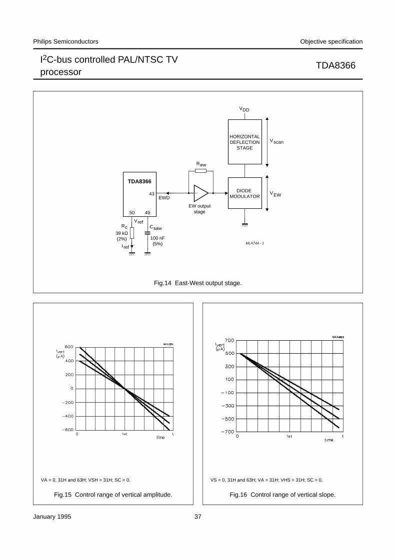
East-West output stage
In order to obtain correct tracking of the vertical andhorizontal EHT-correction, the EW output stage should bedimensioned as illustrated in Fig.14.
Resistor REW determines the gain of the EW output stage.Resistor Rc determines the reference current for both thevertical sawtooth generator and the geometry processor.
The preferred value of Rc is 39 kΩ which results in areference current of 100 µA (Vref = 3.9 V).
The value of REW must be:
Example: With Vref = 3.9 V; Rc = 39 kΩ and Vscan = 120 Vthen REW = 68 kΩ.
REW Rc
Vscan
18 Vref×-----------------------×=
January 1995 37
Philips Semiconductors Objective specification
I2C-bus controlled PAL/NTSC TVprocessor
TDA8366
handbook, full pagewidth
MLA744 - 1
TDA8366
HORIZONTAL DEFLECTION
STAGE
DIODE MODULATOR
VDD
Vscan
VEW
Rew
EW output stage
EWD
Csaw
100 nF (5%)
VrefRc
39 kΩ (2%)
I ref
43
4950
Fig.14 East-West output stage.
Fig.15 Control range of vertical amplitude.
VA = 0, 31H and 63H; VSH = 31H; SC = 0.
Fig.16 Control range of vertical slope.
VS = 0, 31H and 63H; VA = 31H; VHS = 31H; SC = 0.
January 1995 38
Philips Semiconductors Objective specification
I2C-bus controlled PAL/NTSC TVprocessor
TDA8366
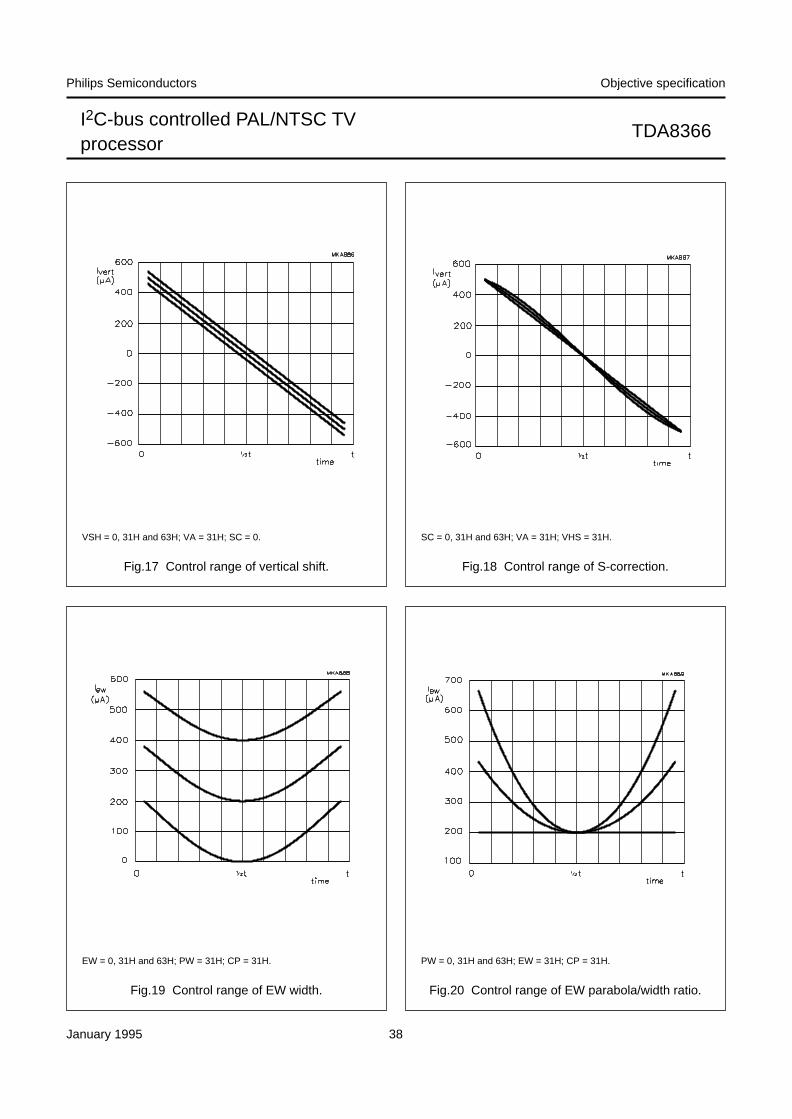
Fig.17 Control range of vertical shift.
VSH = 0, 31H and 63H; VA = 31H; SC = 0.
Fig.18 Control range of S-correction.
SC = 0, 31H and 63H; VA = 31H; VHS = 31H.
Fig.19 Control range of EW width.
EW = 0, 31H and 63H; PW = 31H; CP = 31H.
Fig.20 Control range of EW parabola/width ratio.
PW = 0, 31H and 63H; EW = 31H; CP = 31H.

January 1995 39
Philips Semiconductors Objective specification
I2C-bus controlled PAL/NTSC TVprocessor
TDA8366
Fig.21 Control range of EW corner/parabola ratio.
CP = 0, 31H and 63H; EW = 31H; PW = 63H.
Fig.22 Control range of EW trapezium correction.
TC = 0, 31H and 63H; EW = 31H; PW = 31H.
January 1995 40
Philips Semiconductors Objective specification
I2C-bus controlled PAL/NTSC TVprocessor
TDA8366
Adjustment of geometry control parameters
The deflection processor of the TDA8366 offers ninecontrol parameters for picture alignment:
• Vertical picture alignment
– S-correction
– vertical amplitude
– vertical slope
– vertical shift
• Horizontal picture alignment
– horizontal shift
– EW width
– EW parabola/width
– EW corner/parabola
– EW trapezium correction.
It is important to notice that the TDA8366 is designed foruse with a DC-coupled vertical deflection stage. This is thereason why a vertical linearity alignment is not necessary(and therefore not available).
For a particular combination of picture tube type, verticaloutput stage and EW output stage it is determined whichare the required values for the settings of S-correction, EWparabola/width ratio and EW corner/parabola ratio. Theseparameters can be preset via the I2C-bus, and do not needany additional adjustment. The rest of the parameters arepreset with the mid-value of their control range (i.e. 1FH),or with the values obtained by previous TV-setadjustments.
The vertical shift control is meant for compensation ofoff-sets in the external vertical output stage or in thepicture tube. It can be shown that without compensationthese off-sets will result in a certain linearity error,especially with picture tubes that need large S-correction.The total linearity error is in first order approximationproportional to the value of the off-set, and to the square ofthe S-correction needed. The necessity to use the verticalshift alignment depends on the expected off-sets in verticaloutput stage and picture tube, on the required value of theS-correction, and on the demands upon vertical linearity.
For adjustment of the vertical shift and vertical slopeindependent of each other, a special service blankingmode can be entered by setting the SBL bit HIGH. In thismode the RGB-outputs are blanked during the second halfof the picture. There are 2 different methods for alignmentof the picture in vertical direction. Both methods make useof the service blanking mode.
The first method is recommended for picture tubes thathave a marking for the middle of the screen. With thevertical shift control the last line of the visible picture ispositioned exactly in the middle of the screen. After thisadjustment the vertical shift should not be changed. Thetop of the picture is placed by adjustment of the verticalamplitude, and the bottom by adjustment of the verticalslope.
The second method is recommended for picture tubes thathave no marking for the middle of the screen. For thismethod a video signal is required in which the middle of thepicture is indicated (e.g. the white line in the circle testpattern). With the vertical slope control the beginning of theblanking is positioned exactly on the middle of the picture.Then the top and bottom of the picture are placedsymmetrical with respect to the middle of the screen byadjustment of the vertical amplitude and vertical shift.After this adjustment the vertical shift has the right settingand should not be changed.
If the vertical shift alignment is not required VSH should beset to its mid-value (i.e. VSH = 1F). Then the top of thepicture is placed by adjustment of the vertical amplitudeand the bottom by adjustment of the vertical slope. Afterthe vertical picture alignment the picture is positioned inthe horizontal direction by adjustment of the EW width andthe horizontal shift. Finally (if necessary) the left- andright-hand sides of the picture are aligned in parallel byadjusting the EW trapezium control.
After adjustment of the picture for normal verticaldeflection as described, no additional adjustment isnecessary for the compress and expand mode. If requireda small correction of the picture height can be made byadjusting the vertical slope. This will not effect the linearity.

January 1995 41
Philips Semiconductors Objective specification
I2C-bus controlled PAL/NTSC TVprocessor
TDA8366
PACKAGE OUTLINES
handbook, full pagewidth
1
27
26
1.3 max
14.1 13.7
47.92 47.02
4.57 max
5.08 max
0.51 min
3.2 2.8
seat
ing
plan
e
0.18 M0.53 max
1.778(25x)
1.73 max
15.80 15.24
0.32 max
15.24
17.15 15.90
MSA267
52
Fig.23 Plastic shrink dual in-line package; 52 leads (600 mil) SDIP52; SOT247-1.
Dimensions in mm.

January 1995 42
Philips Semiconductors Objective specification
I2C-bus controlled PAL/NTSC TVprocessor
TDA8366
handbook, full pagewidth
MSA327
1.00.6
detail X
1.41.2
0.250.14
3.22.7
0 to 7o
2.902.65 0.25
0.05
S0.10 Sseating plane
X
A
B
pin 1 index
18.217.6
1.20.8
(4x)
20.119.9
24.223.6
1.0
0.20
MB
0.500.35
0.500.35
1.20.8
(4x)1.0
14.113.9
0.20 M A
1
64 52
51
33
3220
19
Fig.24 Plastic quad flat package; 64 leads (lead length 1.95 mm); body 14 × 20 × 2.8 mm.
Dimensions in mm.

January 1995 43
Philips Semiconductors Objective specification
I2C-bus controlled PAL/NTSC TVprocessor
TDA8366
SOLDERING
Plastic dual in-line packages
BY DIP OR WAVE
The maximum permissible temperature of the solder is260 °C; this temperature must not be in contact with thejoint for more than 5 s. The total contact time of successivesolder waves must not exceed 5 s.
The device may be mounted up to the seating plane, butthe temperature of the plastic body must not exceed thespecified storage maximum. If the printed-circuit board hasbeen pre-heated, forced cooling may be necessaryimmediately after soldering to keep the temperature withinthe permissible limit.
REPAIRING SOLDERED JOINTS
Apply a low voltage soldering iron below the seating plane(or not more than 2 mm above it). If its temperature isbelow 300 °C, it must not be in contact for more than 10 s;if between 300 and 400 °C, for not more than 5 s.
Plastic quad flat-packs
BY WAVE
During placement and before soldering, the componentmust be fixed with a droplet of adhesive. After curing theadhesive, the component can be soldered. The adhesivecan be applied by screen printing, pin transfer or syringedispensing.
Maximum permissible solder temperature is 260 °C, andmaximum duration of package immersion in solder bath is10 s, if allowed to cool to less than 150 °C within 6 s.Typical dwell time is 4 s at 250 °C.
A modified wave soldering technique is recommendedusing two solder waves (dual-wave), in which a turbulentwave with high upward pressure is followed by a smoothlaminar wave. Using a mildly-activated flux eliminates theneed for removal of corrosive residues in mostapplications.
BY SOLDER PASTE REFLOW
Reflow soldering requires the solder paste (a suspensionof fine solder particles, flux and binding agent) to beapplied to the substrate by screen printing, stencilling orpressure-syringe dispensing before device placement.
Several techniques exist for reflowing; for example,thermal conduction by heated belt, infrared, andvapour-phase reflow. Dwell times vary between 50 and300 s according to method. Typical reflow temperaturesrange from 215 to 250 °C.
Preheating is necessary to dry the paste and evaporatethe binding agent. Preheating duration: 45 min at 45 °C.
REPAIRING SOLDERED JOINTS (BY HAND-HELD SOLDERING
IRON OR PULSE-HEATED SOLDER TOOL)
Fix the component by first soldering two, diagonallyopposite, end pins. Apply the heating tool to the flat part ofthe pin only. Contact time must be limited to 10 s at up to300 °C. When using proper tools, all other pins can besoldered in one operation within 2 to 5 s at between 270and 320 °C. (Pulse-heated soldering is not recommendedfor SO packages.)
For pulse-heated solder tool (resistance) soldering of VSOpackages, solder is applied to the substrate by dipping orby an extra thick tin/lead plating before packageplacement.

January 1995 44
Philips Semiconductors Objective specification
I2C-bus controlled PAL/NTSC TVprocessor
TDA8366
DEFINITIONS
LIFE SUPPORT APPLICATIONS
These products are not designed for use in life support appliances, devices, or systems where malfunction of theseproducts can reasonably be expected to result in personal injury. Philips customers using or selling these products foruse in such applications do so at their own risk and agree to fully indemnify Philips for any damages resulting from suchimproper use or sale.
PURCHASE OF PHILIPS I2C COMPONENTS
Data sheet status
Objective specification This data sheet contains target or goal specifications for product development.
Preliminary specification This data sheet contains preliminary data; supplementary data may be published later.
Product specification This data sheet contains final product specifications.
Limiting values
Limiting values given are in accordance with the Absolute Maximum Rating System (IEC 134). Stress above one ormore of the limiting values may cause permanent damage to the device. These are stress ratings only and operationof the device at these or at any other conditions above those given in the Characteristics sections of the specificationis not implied. Exposure to limiting values for extended periods may affect device reliability.
Application information
Where application information is given, it is advisory and does not form part of the specification.
Purchase of Philips I2C components conveys a license under the Philips’ I2C patent to use thecomponents in the I2C system provided the system conforms to the I2C specification defined byPhilips. This specification can be ordered using the code 9398 393 40011.