Embed Size (px)
Citation preview
EM
EX
PL
OR
ER
At
The
Ed
ge
EM
EX
PL
OR
ER
At
The
Ed
ge
Nov. 2009 www.emexplorer.net 1
Dark-field Inspection of Wafer Defects
An EM Explorer Console Tutorial
(updated for v6.3)

EM
EX
PL
OR
ER
At
The
Ed
ge
Nov. 2009 www.emexplorer.net 2
Overview
This tutorial describes, step by step, an example script for wafer
defect inspection simulations using EM Explorer Pro 6.3
The script can be found in the
Examples\dark_field_defect_Inspection\ directory of EM Explorer
distribution
It demonstrates 3 simulation capabilities of EM Explorer Pro 6.3
FDTD simulation of wafer near field
Calculation of far-field spectrum of the reflected field in free space
Imaging of the reflected field onto a detector thru a lens, a
frequency filter and a polarizer
EM
EX
PL
OR
ER
At
The
Ed
ge
Nov. 2009 www.emexplorer.net 3
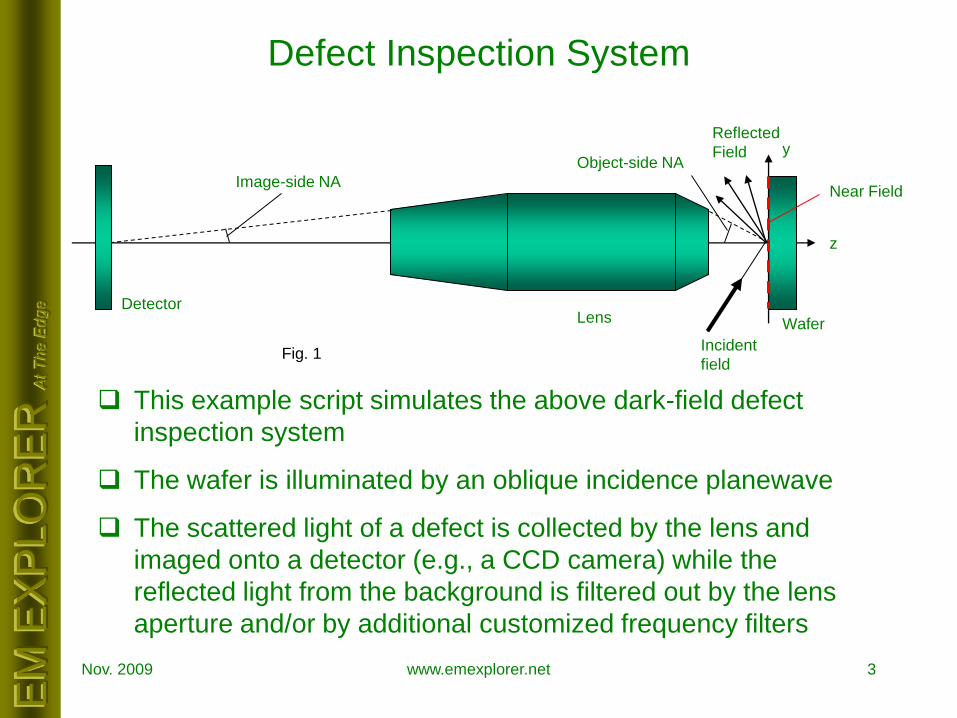
Defect Inspection System
This example script simulates the above dark-field defect
inspection system
The wafer is illuminated by an oblique incidence planewave
The scattered light of a defect is collected by the lens and
imaged onto a detector (e.g., a CCD camera) while the
reflected light from the background is filtered out by the lens
aperture and/or by additional customized frequency filters
z
y
Wafer
Incident
field
Reflected
Field
Near Field
LensDetector
Image-side NA
Object-side NA
Fig. 1

EM
EX
PL
OR
ER
At
The
Ed
ge
Nov. 2009 www.emexplorer.net 4
Script Organization
The simulations are run inside two nested loops in the script Outer loop over wafer patterns:
Case 1: a defect-free line/space wafer pattern
Case 2: a void in a metal line (open circuit)
Case 3: a defect in between metal lines (short circuit)
Inner loop over incident field polarizations: s- and p-polarization
[Definition of variables, e.g., wavelength, angle of incidence, material n&k, etc… ]
foreach CASE {1 2 3} {
foreach POL {S P} {
[Part 1: FDTD simulation of wafer near field]
[Part 2: Calculation of far-field spectrum of the reflected field]
[Part 3: Imaging the reflected field thru a lens, a filter and a polarizer]
}
}
EsEp
K
Case 3
defect
x
z
y
EsEp
K
Case 2
defect
x
z
y
EsEp
K
Case 1
x
z
y
Fig.2

EM
EX
PL
OR
ER
At
The
Ed
ge
Nov. 2009 www.emexplorer.net 5
Script Organization (cont’d)
In the script, variables are heavily used to parameterize the simulation conditions.
For example, the command for FDTD grid setup is written as
emxp::grid lx=$LX ly=$LY lz=$LZ nx=$NX ny=$NY nz=$NZ n0=1 k0=0
where LX, LY, LZ, etc…, in red are variables defined at the beginning of the script.
The “$” sign indicates they need to be substituted with actual values at the run
time.
Parameterization is very useful in writing a script that can be easily adapted for
different conditions, particularly when it comes to looping and geometry creation.
For the sake of clarity, we will substitute the variables with the actual values
assigned to them when we explain each of the commands in this tutorial. In fact,
this is also the process taking place when the script is executed by the program.
So the above command becomes as follows.
emxp::grid lx=3.0 ly=3.0 lz=0.8 nx=75 ny=75 nz=20 n0=1 k0=0
Sometimes the user may encounter some special characters in the script.
Lines starting with “#” sign are comments and are ignored by the program
Lines ending with “\” indicates the command is not yet complete and continues
to the next line

EM
EX
PL
OR
ER
At
The
Ed
ge
Nov. 2009 www.emexplorer.net 6
How to run the script
To run the script, type the following command in Windows shell
"C:\EM Explorer\EM Explorer Studio\bin\emxp.exe" dark_field_defect_inspection.emx
The first item in quote is the full filename path to the EM Explorer Console
executable (emxp.exe).
The above assumes that the user has installed the package in the
default directory. If not, it needs to be substituted with the actual path.
The second item is the script filename (dark_field_defect_inspect.emx)
The user can place the above command in a .bat file (e.g., runemx.bat) and
then executes the command by simply double-clicking the .bat file.

EM
EX
PL
OR
ER
At
The
Ed
ge
Nov. 2009 www.emexplorer.net 7
Part 1
FDTD simulation of wafer near field
Step 1: Setup FDTD Grid
Step 2: Setup FDTD Geometry
Step 3: Setup FDTD Excitation
Step 4: Setup FDTD Boundary Condition
Step 5: Setup FDTD Convergence Monitor
Step 6: Run FDTD Solver
Step 7: Output FDTD Data

EM
EX
PL
OR
ER
At
The
Ed
ge
Nov. 2009 www.emexplorer.net 8
Step 1: Setup FDTD Grid
emxp::grid lx=3.0 ly=3.0 lz=0.8 nx=75 ny=75 nz=20 n0=1 k0=0
emxp::grid is the command name for FDTD grid specification
lx, ly and lz are FDTD simulation domain sizes in x, y and z directions respectively.
Note all length units in this example are in um.
nx, ny and nz are number of Yee cells in x, y and z directions respectively
Note, in this example, lx/nx = ly/ny = lz/nz = 0.04um, which is the Yee cell size.
For tutorial purpose, a relatively large Yee cell size (~1/9 of the wavelength = 0.364um, see
excitation setup) is used so that the simulation can run quickly. For better accuracy, <1/15
of wavelength is generally recommended.
It is also recommended to have approximately the same Yee cell size in all three (x, y, z)
directions to minimize numerical dispersion.
n0 and k0 are the real and imaginary part of the complex refractive index of the ambient
material, which is air in this example.
Command
Explanation
EM
EX
PL
OR
ER
At
The
Ed
ge
Nov. 2009 www.emexplorer.net 9
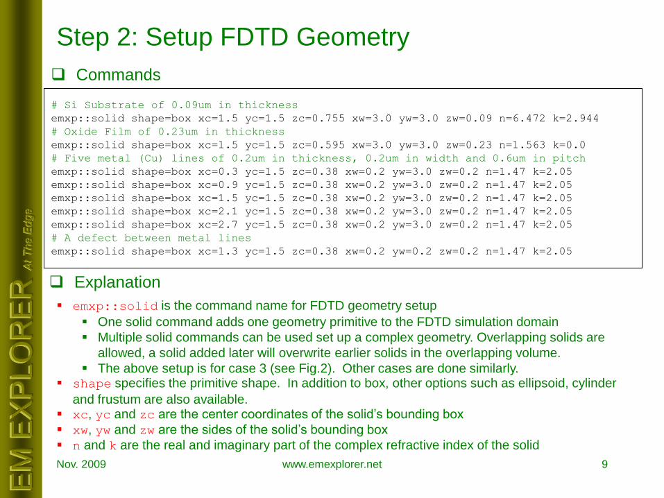
Step 2: Setup FDTD Geometry
Commands
Explanation
emxp::solid is the command name for FDTD geometry setup
One solid command adds one geometry primitive to the FDTD simulation domain
Multiple solid commands can be used set up a complex geometry. Overlapping solids are
allowed, a solid added later will overwrite earlier solids in the overlapping volume.
The above setup is for case 3 (see Fig.2). Other cases are done similarly. shape specifies the primitive shape. In addition to box, other options such as ellipsoid, cylinder
and frustum are also available. xc, yc and zc are the center coordinates of the solid’s bounding box
xw, yw and zw are the sides of the solid’s bounding box
n and k are the real and imaginary part of the complex refractive index of the solid
# Si Substrate of 0.09um in thickness
emxp::solid shape=box xc=1.5 yc=1.5 zc=0.755 xw=3.0 yw=3.0 zw=0.09 n=6.472 k=2.944
# Oxide Film of 0.23um in thickness
emxp::solid shape=box xc=1.5 yc=1.5 zc=0.595 xw=3.0 yw=3.0 zw=0.23 n=1.563 k=0.0
# Five metal (Cu) lines of 0.2um in thickness, 0.2um in width and 0.6um in pitch
emxp::solid shape=box xc=0.3 yc=1.5 zc=0.38 xw=0.2 yw=3.0 zw=0.2 n=1.47 k=2.05
emxp::solid shape=box xc=0.9 yc=1.5 zc=0.38 xw=0.2 yw=3.0 zw=0.2 n=1.47 k=2.05
emxp::solid shape=box xc=1.5 yc=1.5 zc=0.38 xw=0.2 yw=3.0 zw=0.2 n=1.47 k=2.05
emxp::solid shape=box xc=2.1 yc=1.5 zc=0.38 xw=0.2 yw=3.0 zw=0.2 n=1.47 k=2.05
emxp::solid shape=box xc=2.7 yc=1.5 zc=0.38 xw=0.2 yw=3.0 zw=0.2 n=1.47 k=2.05
# A defect between metal lines
emxp::solid shape=box xc=1.3 yc=1.5 zc=0.38 xw=0.2 yw=0.2 zw=0.2 n=1.47 k=2.05

EM
EX
PL
OR
ER
At
The
Ed
ge
Nov. 2009 www.emexplorer.net 10
Step 3: Setup FDTD Excitation
Command
emxp::planewave2 wavelength=0.364 z_source=0.2 es_amp=0.0 ep_amp=1.0 theta=50 phi=0
emxp::planewave2 is the command name to set up a planewave excitation.
There is also emxp::planewave command which specifies a planewave in a different way.
wavelength is the planewave wavelength in vacuum.
z_source specifies the z location of the excitation source plane. The source plane is
perpendicular to z axis.
Total field / scattered field method is used to model the planewave source. The source
plane divides the simulation domain into a total field region (z > z_source) and a reflected
field region (z < z_source).
es_amp (ep_amp) is the amplitude of the s-polarization (p-polarization) component of the
incident electric field
s-polarization component Es is perpendicular to the plane of incidence
p-polarization component Ep is parallel to the plane of incidence
Note Es, Ep and wavevecor K are orthogonal to each other (see Fig.2)
The above example specifies a p-polarized incident field.
theta and phi are the angles to specify the planewave wavevector K in degree.
phi is the angle between the plane of incidence and x-z plane
theta is the angle between the wavevector K and z axis
In this example, the plane of incidence coincides with x-z plane and K is 50 from normal
Explanation

EM
EX
PL
OR
ER
At
The
Ed
ge
Nov. 2009 www.emexplorer.net 11
Step 4: FDTD Boundary Condition
Command
EM Explorer assumes the following boundary conditions
Periodic boundary condition (PBC) in x and y
Absorbing boundary condition (ABC) in z. Sometimes this is also called open BC.
The following methods are available in EM Explorer to model the ABC
Analytical ABC
PML (Perfectly Matching Layer) ABC
PML2 ABC, which is an enhanced version of PML.
We use pml2 in this example
Explanation
emxp::pml2

EM
EX
PL
OR
ER
At
The
Ed
ge
Nov. 2009 www.emexplorer.net 12
Step 5: FDTD Convergence Monitor
Command
The convergence monitor checks the electric field amplitude at a user-specified location to see if
it reaches steady state based on user-specified criterion.
i, j, and k are the indices of the Yee cell where the field is monitored.
In this example, it monitors the (0,0,0) cell for the reflected field (recall that at this location z
< z_source)
samples_per_cycle is the frequency at which the data will be collected.
In this example, the reflected field will be sampled once every wave cycle.
sample_size is the number of data points on which the maximum and minimum values of data
are calculated. The calculation is done on the most recent data collected.
In this example, the last 10 data points collected will be used to compute the max and min
values.
tolerance is the user-specified steady state criterion.
If tolerance < max-min, then the steady state is reached and the FDTD solver stops running.
If the condition is not met, the FDTD solver will continue to run until the maximum number of
cycles specified by the user is reached (see step 6 for details). In this example, since
tolerance=0.0, the solver will run to the max cycles.
Explanation
emxp::convergence i=0 j=0 k=0 sample_size=10 samples_per_cycle=1 tolerance=0.00

EM
EX
PL
OR
ER
At
The
Ed
ge
Nov. 2009 www.emexplorer.net 13
Step 6: Run FDTD Solver
Command
emxp::run command runs the FDTD solver to propagate the electromagnetic field through the
simulation domain. It solves the Maxwell’s equations using a field marching algorithm in time
domain. n_cycles specifies the maximum number of wave cycles that the above process to run.
One wave cycle means the monoharmonic field oscillates one period in time or travels one
wavelength in space.
The FDTD solver stops when n_cycles is reached or when the convergence criterion is met
(see step 5)
Note
Meshing is also done in this step if it is not done yet.
This command can be called repeatedly to continue the field propagation. The user can
output intermediate results (see step 7) if needed between the run commands.
Below is an example screen output when this command is called
Explanation
emxp::run n_cycles=20
emxp> emxp::run n_cycles=20
Building Mesh: 0%----10%----20%----30%----40%----50%----60%----70%----80%----90%----100%
Cycle= 1.00 Ex= 0.01903 -2.62860 Ey= 0.00000 2.30684 Ez= 0.02403 2.74025
Cycle= 2.00 Ex= 0.02457 1.50301 Ey= 0.00000 -1.25017 Ez= 0.02938 2.39990
Cycle= 3.00 Ex= 0.11084 0.88072 Ey= 0.00000 2.54462 Ez= 0.12835 0.22910
... ...

EM
EX
PL
OR
ER
At
The
Ed
ge
Nov. 2009 www.emexplorer.net 14
Step 7: Output FDTD Results
Command
emxp::output command is used to save FDTD result to a file.
property specifies what to output. It can save complex E- and H-field, intensity, Poynting
vector, complex permittivity and permeability throughout the simulation domain.
In this example, we save e-field intensity
imin, imax, jmin, jmax, kmin, kmax specify a spatial range of Yee cells of which the
data to be saved.
In this example, we save the intensity distribution in the plane at z=0, which is part of the
reflected field.
file is the filename to which the data is saved.
It is in standard VTK format. Therefore any VTK-compatible data visualizers (e.g., MayaVi,
ParaView, etc…) can be used to view the data.
It is also in text format, which allows the user to easily import to his/her own applications to
extract the information
Explanation
emxp::output property=intensity imin=0 imax=75 jmin=0 jmax=75 kmin=0 kmax=0 \
file=intensity_nearfield_z0_Case3_P_0.04.vtk

EM
EX
PL
OR
ER
At
The
Ed
ge
Nov. 2009 www.emexplorer.net 15
Example FDTD Near Field Results
Reflected Field Intensity Distribution at z = 0
Case 1
S-Polarization
Case 2
S-Polarization
Case 3
S-Polarization
Case 1
P-Polarization
Case 2
P-Polarization
Case 3
P-Polarization
Fig.3

EM
EX
PL
OR
ER
At
The
Ed
ge
Nov. 2009 www.emexplorer.net 16
Part 2
Calculation of far-field spectrum of
the reflected field in free space
z
y
WaferIncident field
Reflected Field
Near Field
Far Field
Step 1: Setup Near Field
Step 2: Propagate to Far Field
Fig. 4

EM
EX
PL
OR
ER
At
The
Ed
ge
Nov. 2009 www.emexplorer.net 17
Step 1: Setup Near Field
Command
emxp::nearfield command is used to setup the near field of the simulation engine
object specifies where the near field comes from
In this example, it comes from the FDTD simulation engine
Other options are also available, such as from external data files
k specifies the z index of the plane location in which the FDTD near field is sampled.
In this example, the reflected field at z=0 is sampled (recall that z=0 < z_source, which is in
the reflected field region)
Explanation
emxp::nearfield object=FDTD k=0

EM
EX
PL
OR
ER
At
The
Ed
ge
Nov. 2009 www.emexplorer.net 18
Step 2: Propagate to Far Field
Command
emxp::propagate command propagates the near field to far field
medium specifies the object through which the field propagates
In this example, it is just an open space
Other options are also available, such as lens, filters, etc…
distance specifies the distance over which the field propagates.
In this example, this distance is 1mm, large enough (compared to the wavelength) for the
evanescent waves to die out.
output specifies a filename to save results
property specifies what to save. In this example, the property is the intensity of the Fourier
transform of the far field as indicated by “ft_intensity”, which is also called the spectrum or
diffraction orders of the scattered field.
Explanation
emxp::propagate medium=freespace distance=1000.0 \
output=ft_intensity_Case3_P_0.04.vtk property=ft_intensity

EM
EX
PL
OR
ER
At
The
Ed
ge
Nov. 2009 www.emexplorer.net 19
Example Spectrum ResultsCase 1
S-Polarization
Case 2
S-Polarization
Case 1
P-Polarization
Case 2
P-Polarization
Case 3
P-Polarization
Case 3
S-Polarization
Note, a small color scale is used in the above plots in order to show the diffraction
orders of the defects. The background scattering by the metal lines (0th, -5th, and -10th
orders as shown in Case 1) is much stronger and saturated in color.
Fig. 5
0th-order
-5th-order
-10th-order
EM
EX
PL
OR
ER
At
The
Ed
ge
Nov. 2009 www.emexplorer.net 20
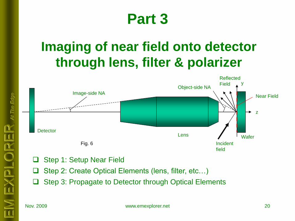
Part 3
Imaging of near field onto detector
through lens, filter & polarizer
Step 1: Setup Near Field
Step 2: Create Optical Elements (lens, filter, etc…)
Step 3: Propagate to Detector through Optical Elements
z
y
Wafer
Incident
field
Reflected
Field
Near Field
LensDetector
Image-side NA
Object-side NA
Fig. 6

EM
EX
PL
OR
ER
At
The
Ed
ge
Nov. 2009 www.emexplorer.net 21
Step 1: Setup Near Field
Command
emxp::nearfield command is used to setup the near field of the simulation engine
object specifies where the near field comes from
In this example, it comes from the FDTD simulation engine
Other options are also available, such as from external data files
k specifies the z index of the plane location in which the FDTD near field is sampled.
In this example, the reflected field at z=0 is sampled (recall that z=0 < z_source, which is in
the reflected field region)
Explanation
emxp::nearfield object=FDTD k=0

EM
EX
PL
OR
ER
At
The
Ed
ge
Nov. 2009 www.emexplorer.net 22
Step 2: Create Optical Elements (1)
Command for creating a lens
emxp::lens command creates an optical lens element in EM Explorer
mag specifies the magnification of the lens
Note a large magnification (100x) is used in this example
n_obj is the refractive index of the medium in the object space
n_img is the refractive index of the medium in the image space
na specifies the Numerical Aperture (NA) of the lens on the image side.
The NA on the object side is na_obj = na * mag
Note in this example, the image-side NA is very small (na=0.005), therefore all light rays in
the image space are nearly parallel to the optical axis
In the object space, na_obj = 0.5 ( < n_obj * sin(50) ), therefore 0th-order scattered light
produced by the background metal lines will be filtered out by the lens (see Fig.5). This is a typical setup of dark-field imaging for defect detection.
Explanation
emxp::lens mag=100.0 n_obj=1.0 n_img=1.0 na=0.005

EM
EX
PL
OR
ER
At
The
Ed
ge
Nov. 2009 www.emexplorer.net 23
Step 2: Create Optical Elements (2)
Command for creating a spatial frequency filter
emxp::freq_filter command creates a new spatial frequency filter or sets the property of an
existing one name is the reference to the filter. Multiple filters can be created using different names.
property specifies what property to set by the command - background or diffraction order
m & n are the x & y indices to a diffraction order of the field
trans specifies the transmission of the background or the diffraction order
Note, in this example, the system is designed to filter out 3 diffraction orders of the reflected field.
These are the main diffraction orders (0th, -5th, -10th orders) produced by the background metal
lines (see Part 2 simulation results). Note, the 0th-order is already filtered out by the previous
lens aperture. The –5th and –10th orders are filtered by this filter.
Explanation
# Specify the background transmission of the filer
emxp::freq_filter name=filter1 property=background trans=1.0
# Specify transmission of diffraction orders
emxp::freq_filter name=filter1 property=diffraction_order m= -5 n=0 trans=0.0
emxp::freq_filter name=filter1 property=diffraction_order m=-10 n=0 trans=0.0
EM
EX
PL
OR
ER
At
The
Ed
ge
Nov. 2009 www.emexplorer.net 24
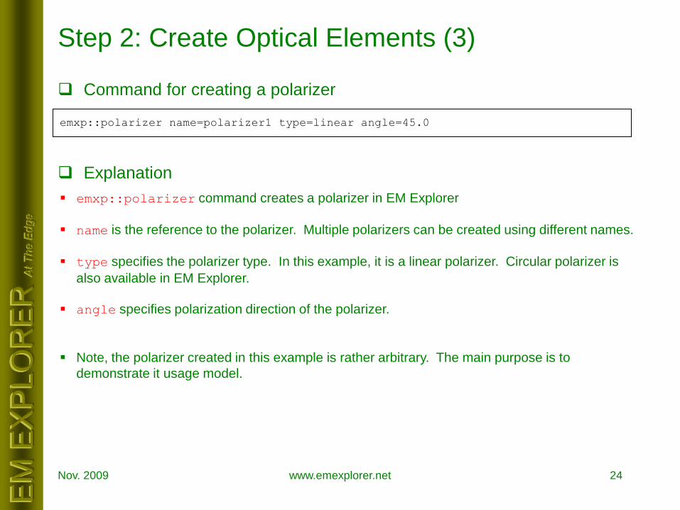
Step 2: Create Optical Elements (3)
Command for creating a polarizer
emxp::polarizer command creates a polarizer in EM Explorer
name is the reference to the polarizer. Multiple polarizers can be created using different names.
type specifies the polarizer type. In this example, it is a linear polarizer. Circular polarizer is
also available in EM Explorer.
angle specifies polarization direction of the polarizer.
Note, the polarizer created in this example is rather arbitrary. The main purpose is to
demonstrate it usage model.
Explanation
emxp::polarizer name=polarizer1 type=linear angle=45.0

EM
EX
PL
OR
ER
At
The
Ed
ge
Nov. 2009 www.emexplorer.net 25
Step 3: Propagate thru Optical Elements
Commands
The above commands are quite self-explanatory.
By cascading the propagate commands, the field is modified by the optical elements in series.
Explanation
# Propagate the field through the lens
emxp::propagate medium=lens defocus=0.0 \
output=intensity_lens_Case3_P_0.04.vtk property=intensity
# Apply the filter to the field
emxp::propagate medium=filter1 \
output=intensity_filter_Case3_P_0.04.vtk property=intensity
# Apply the polarizer to the field
emxp::propagate medium=polarizer1 \
output=intensity_polarizer_Case3_P_0.04.vtk property=intensity

EM
EX
PL
OR
ER
At
The
Ed
ge
Nov. 2009 www.emexplorer.net 26
Example Defect Images at the Detector
Case 1
S-Polarization
Case 2
S-Polarization
Case 3
S-Polarization
Case 1
P-Polarization
Case 2
P-Polarization
Case 3
P-Polarization
Images through lens only (no filter or polarizer)
Note the small color scale due to the intensity dilution from the 100x magnification lens
It’s not easy to distinguish between Case 2 defect and Case 3 defect at the detector
Fig. 7

EM
EX
PL
OR
ER
At
The
Ed
ge
Nov. 2009 www.emexplorer.net 27
Example Defect Images at the Detector
Case 1
S-Polarization
Case 2
S-Polarization
Case 3
S-Polarization
Case 1
P-Polarization
Case 2
P-Polarization
Case 3
P-Polarization
Images through lens and filter (no polarizer)
Note the defect image intensity is strongly dependent on the polarization in Case 3
defect, which can be used to distinguish it from Case 2 defect.
Fig. 8

EM
EX
PL
OR
ER
At
The
Ed
ge
Nov. 2009 www.emexplorer.net 28
Thank You