Embed Size (px)
Citation preview

http : e.co.kr
Color Television
CHASSIS : CP-185L and CP-185G
Specification
S/M No. : TCP185LGF0
Version Pal multi system
TV Standard PAL-SECAM B/G, D/K, H, I/I (NTSC : AV Only)
Sound system Mono
* 1 Speaker
Power consumption14":49W / 20":60W / 21" 68W* 2Speaker14":57W / 20":64W / 21":74W
Speaker 3W 8 Ohm o 7.5W 8 Ohm
Teletext system Option
Aerial Input 75 Ohm unbalanced
Channel coverage off-air channels, S-cable channels and hyperband
Tuning system Ferquency synthesiser tuning system
14":34cmVisual screen size 20’:48cm
21":51cm
Channel indication On screen display
Program selection 100 Programmes
RCA jack : Audio input and Vidio inputERUO SCART Jack : Audio/Video and R/G/B input.
Auxiliary Outpup Terminal Sloe and fast swtching, SVHsinAudio - Video jack on front of cabinet in commonconnection with EURO-SCART Headphone jack on front of cabinet
R-40A10 (None teletext) AAA Battery typeRemote control R-40A01(With teletext) AAA Battery type
R-44C05(With teletext) AA Battery type
Jul. 2003
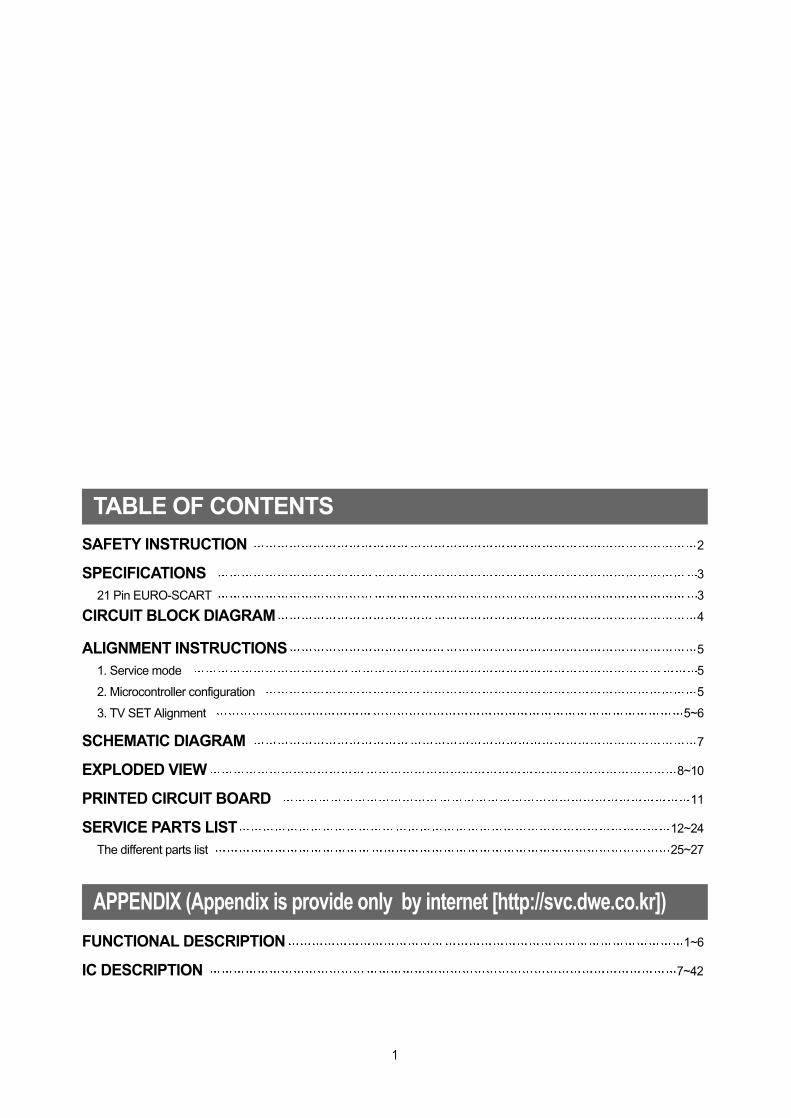
SAFETY INSTRUCTION 2
SPECIFICATIONS 3
21 Pin EURO-SCART 3
CIRCUIT BLOCK DIAGRAM 4
ALIGNMENT INSTRUCTIONS 5
1. Service mode 5
2. Microcontroller configuration 5
3. TV SET Alignment 5~6
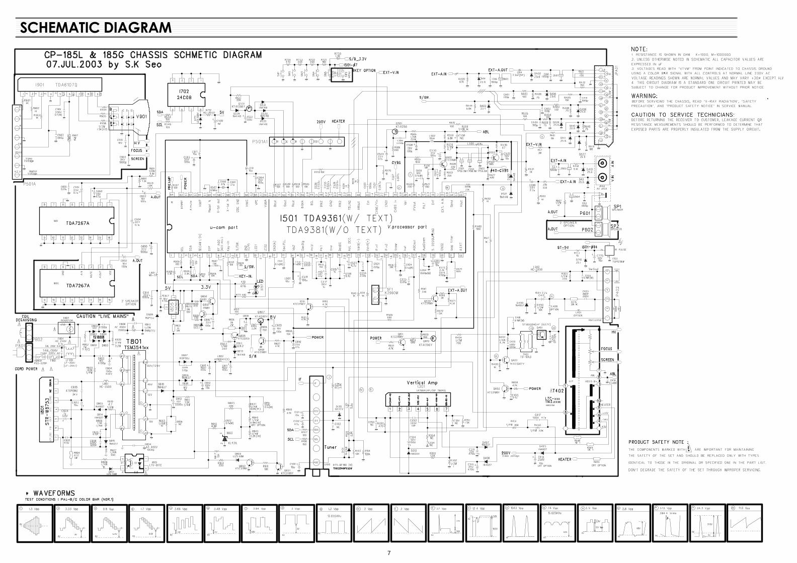
SCHEMATIC DIAGRAM 7
EXPLODED VIEW 8~10
PRINTED CIRCUIT BOARD 11
SERVICE PARTS LIST 12~24
The different parts list 25~27
FUNCTIONAL DESCRIPTION 1~6
IC DESCRIPTION 7~42
1
TABLE OF CONTENTS
APPENDIX (Appendix is provide only by internet [http://svc.dwe.co.kr])
2
X-RAY RADIATION PRECAUTION
1. Excessive high voltage can produce potentially hazardous X-RAY RADIATION. To avoid such hazards, the highvoltage must not exceed the specified limit. The nominal value of the high voltage of this receiver is 22-23 kV (14")or24-26 kV (20"-21")at max beam current. The high voltage must not, under any circumstances, exceed 27.5 kV (14",20"), 29KV (21"). Each time a receiver requires servicing, the high voltage should be checked. It is important to use anaccurate and reliable high voltage meter.).
2. The only source of X-RAY Radiation in this TV receiver is the picture tube. For continued X-RAY RADIATIONprotection, the replacement tube must be exactly the same type tube as specified in the parts list.
SAFETY PRECAUTION
1. Potentials of high voltage are present when this receiver is operating. Operation of the receiver outside the cabinet orwith the back cover removed involves a shock hazard from the receiver.1) Servicing should not be attempted by anyone who is not thoroughly familiar with the precautions necessary when
working on high voltage equipment. 2) Discharge the high potential of the picture tube before handling the tube. The picture tube is highly evacuated and if
broken, glass fragments will be violently expelled.2. If any Fuse in this TV receiver is blown, replace it with the FUSE specified in the Replacement Parts List. 3. When replacing a high wattage resistor (oxide metal film resistor) in circuit board, keep the resistor body 10 mm away
from the circuit board.4. Keep wires away from high voltage or high temperature components.5. This receiver must operate under AC 230 volts, 5O Hz. NEVER connect to a DC supply of any other voltage or
frequency.
PRODUCT SAFETY NOTICE
Many electrical and mechanical parts in this equipment have special safety-related characteristics. These characteristicsare often passed unnoticed by a visual inspection and the X-RAY RADIATION protection afforded by them cannotnecessarily be obtained by using replacement components rated for higher voltage, wattage, etc. Replacement partswhich have these spe- cial safety characteristics are identified in this manual and its supplements, electrical componentshaving such features are identified by designated symbol on the parts list. Before replacing any of these components,read the parts list in this manual carefully. The use of substitutes replacement parts which do not have the same safetycharacteristics as specified in the parts list may create X-RAY Radiation.
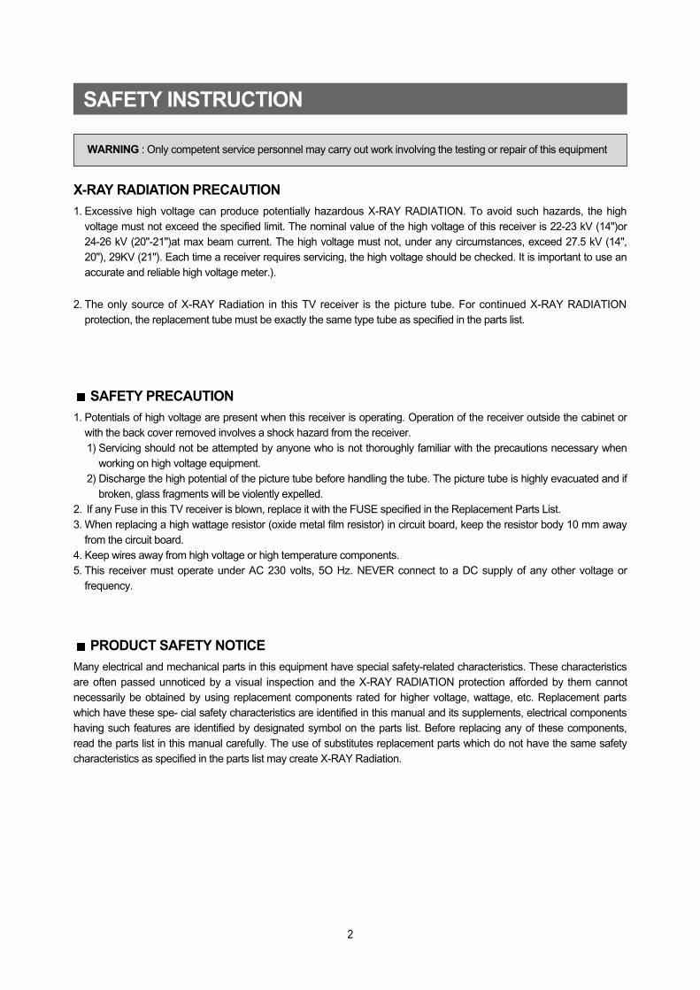
SAFETY INSTRUCTION
WARNING : Only competent service personnel may carry out work involving the testing or repair of this equipment
3
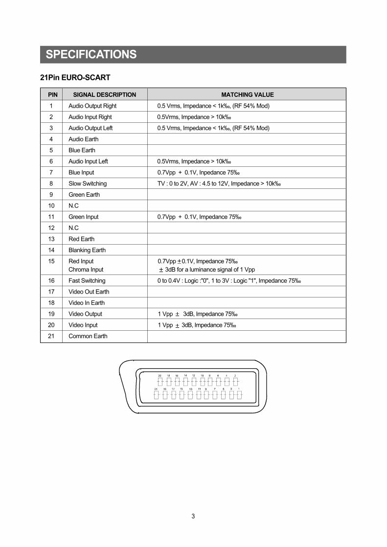
PIN SIGNAL DESCRIPTION MATCHING VALUE
1 Audio Output Right 0.5 Vrms, Impedance < 1k‰, (RF 54% Mod)
2 Audio Input Right 0.5Vrms, Impedance > 10k‰
3 Audio Output Left 0.5 Vrms, Impedance < 1k‰, (RF 54% Mod)
4 Audio Earth
5 Blue Earth
6 Audio Input Left 0.5Vrms, Impedance > 10k‰
7 Blue Input 0.7Vpp + 0.1V, Inpedance 75‰
8 Slow Switching TV : 0 to 2V, AV : 4.5 to 12V, Impedance > 10k‰
9 Green Earth
10 N.C
11 Green Input 0.7Vpp + 0.1V, Impedance 75‰
12 N.C
13 Red Earth
14 Blanking Earth
15 Red Input 0.7Vpp 0.1V, Impedance 75‰Chroma Input 3dB for a luminance signal of 1 Vpp
16 Fast Switching 0 to 0.4V : Logic :"0", 1 to 3V : Logic "1", Impedance 75‰
17 Video Out Earth
18 Video In Earth
19 Video Output 1 Vpp 3dB, Impedance 75‰
20 Video Input 1 Vpp 3dB, Impedance 75‰
21 Common Earth
21Pin EURO-SCART
SPECIFICATIONS
4
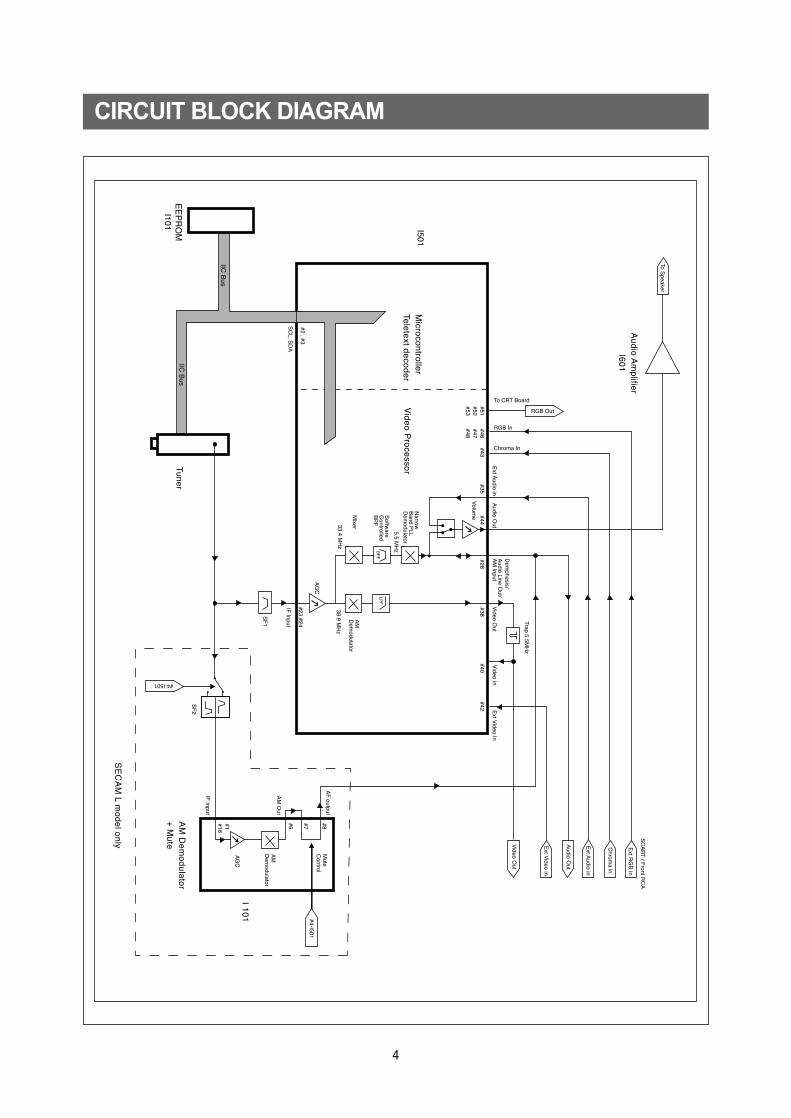
CIRCUIT BLOCK DIAGRAM
5
Microcontroller configuration : Service mode
To switch the TV set into service mode please see instruction below.
1 - Select pr. number 912 - Adjust sharpness to minimum and exit all menu. 3 - Quickly press the key sequence : RED - GREEN - menu
To exit SERVICE menu press menu key or Std By key.
In Service Mode press "OK" to the microcontroller i.e. the I2C bus is free and the set can be controlled by externalequipment.Press "OK" again to allow the microcontroller to control the set again
Microcontroller configuration :
Tuner Option
TV set Alignment
1 - G2 alignment- Set TV in NORMAL I mode- TV in AV mode without video signal ? Black screen.- TV preset with WP Red, WP Green and WP Blue equal to 32.- TV preset with Black R, Black G equal to 8. - Adjust screen volume ( on FBT ) such that the highest cathode cut-off voltage measured on CRT board, is Vcut-off 5V
2 - White balance - Select a dark picture and adjust Black G and Black R to the desired colour temperature.- Select a bright picture and adjust WP Red, WP Green, WP Blue to the desired colour temperature.
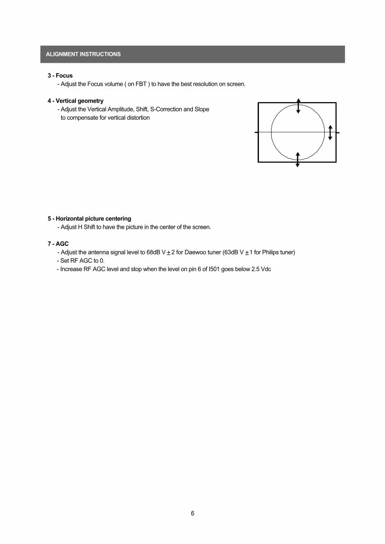
ALIGNMENT INSTRUCTIONS
Option Tuner maker
DW DAEWOO / SAMSUNG
PHI LIPS (tuner internal AGC )
PH2 PHILIPS ( Video processor AGC )
Screen size Vcut-off
14" 115V
20" & 21" 125V
6
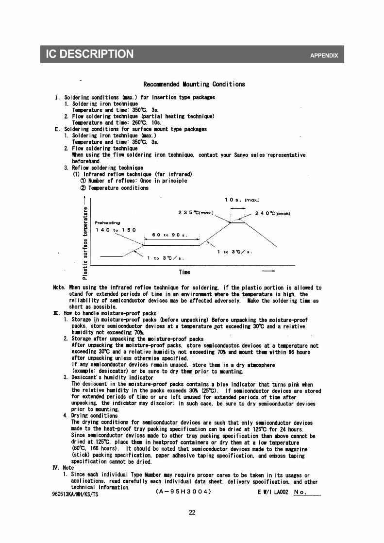
3 - Focus- Adjust the Focus volume ( on FBT ) to have the best resolution on screen.
4 - Vertical geometry - Adjust the Vertical Amplitude, Shift, S-Correction and Slope to compensate for vertical distortion
5 - Horizontal picture centering - Adjust H Shift to have the picture in the center of the screen.
7 - AGC - Adjust the antenna signal level to 68dB V 2 for Daewoo tuner (63dB V 1 for Philips tuner)- Set RF AGC to 0.- Increase RF AGC level and stop when the level on pin 6 of I501 goes below 2.5 Vdc
ALIGNMENT INSTRUCTIONS
7
88
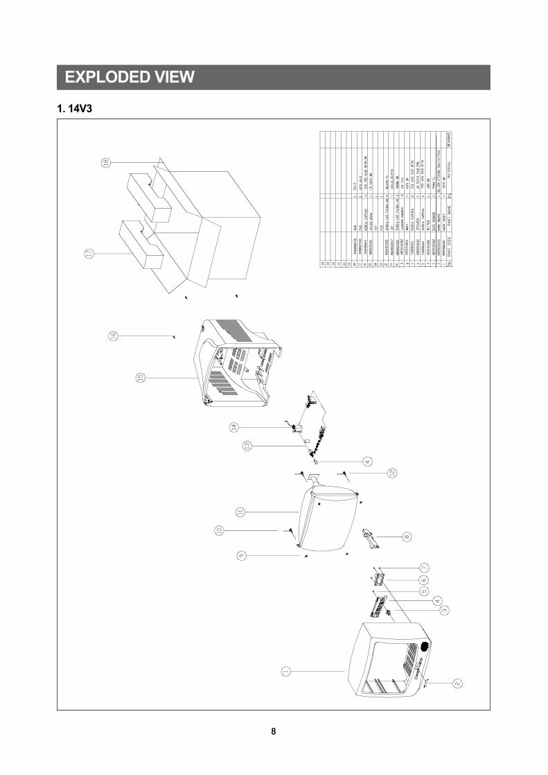
1. 14V3
EXPLODED VIEW
99
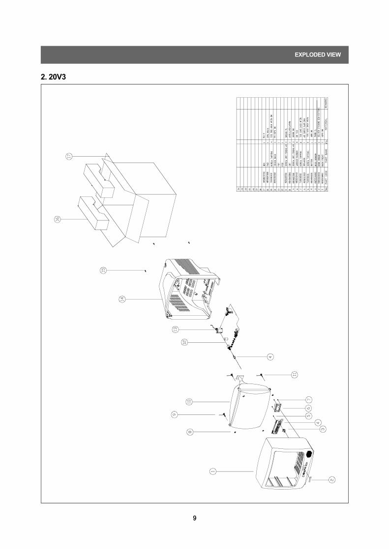
2. 20V3
EXPLODED VIEW
1010
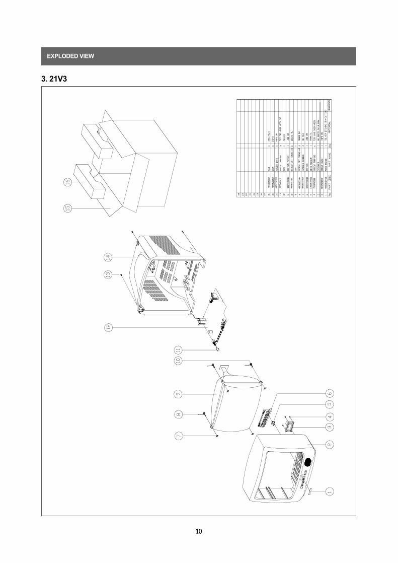
3. 21V3
EXPLODED VIEW
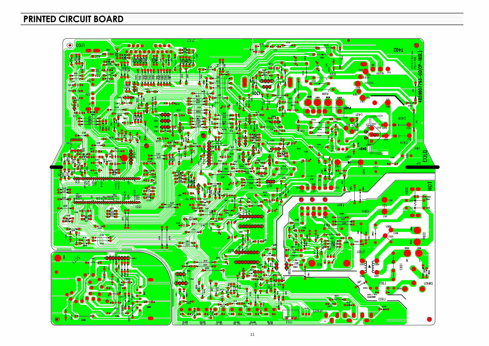
11
12
LOC PART CODE PART NAME DESCRIPTION REMARK
12
ZZ100 48B3740A01 TRANSMITTER REMOCON R-40A01 R
ZZ110 PTACPWD434 ACCESSORY AS DTA-20V1MZ
00100 4850Q00910 BATTERY R03/NN
00200 48586002E2 MANUAL INSTRUCTION ENGLISH,ARABIC
M821 4858213801 BAG INSTRUCTION L.D.P.E T0.05X250X400
ZZ120 PTBCSHD753 COVER BACK AS DTB-21D4T
M211 4852156721 COVER BACK HIPS(CORE A2,B1)
M541 4855415800 SPEC PLATE 150ART P/E FILM (C/TV)
M781 4857817610 CLOTH BLACK FELT 300X20X0.7
ZZ130 PTPKCPD753 PACKING AS DTB-21D4T
10 6520010100 STAPLE PIN AUTO W65
M801 4858057500 BOX CARTON DW-3
M811 4858194100 PAD EPS
M821 4858211801 BAG P.E L.D.P.E T0.03X1300X1100
ZZ131 48519A5310 CRT GROUND NET 2101S-1015-1P
ZZ132 58G0000147 COIL DEGAUSSING DC-21SF !
ZZ140 PTCACAD753 CABINET AS DTB-21D4T
M201A 4856013300 SCREW CRT FIXING 30X80 BK
M201B 4856215402 WASHER RUBBER CR T2.0
M201C 4856013302 SCREW CRT FIXING 30X190 BK
M211A 7172401412 SCREW TAPPTITE TT2 TRS 4X14 MFZN BK
M211B 4855930901 DECO TERM PVC CL T0.2
M211D 7172401412 SCREW TAPPTITE TT2 TRS 4X14 MFZN BK
M591 4855933901 DECO WOOFER HIPS GY
M591A 7172401212 SCREW TAPPTITE TT2 TRS 4X12 MFZNBK
M681 4856812001 TIE CABLE NYLON66 DA100
SP01A 7172401212 SCREW TAPPTITE TT2 TRS 4X12 MFZNBK
SP02A 7172401212 SCREW TAPPTITE TT2 TRS 4X12 MFZNBK
V901 PSRTPWD002 CRT AS A51EHW135X01(PHILIPS) R !
ZRT10 4859637160 CRT A51EHW135X01
ZZ200 PTFMSJD753 MASK FRONT AS DTB-21D4T
M191 4854946301 BUTTON ABS BK
M191A 7178301011 SCREW TAPPTITE TT2 WAS 3X10 MFZN
M201 4852074601 MASK FRONT HIPS BK
M231 4851114411 PANEL CONTROL ASSY 2326711+4857101+6717900
M251 4852540801 GRILL R EGI T0.8
M252 4852540701 GRILL L EGI T0.8
M531 4855313201 DECO COVER HIPS GY
M531A 7178300811 SCREW TAPPTITE TT2 WAS 3X8 MFZN
M561 4855617500 MARK BRAND CU AU+ABS BK
ZZ210 PTSPPWD753 SPEAKER AS DTB-21D4T
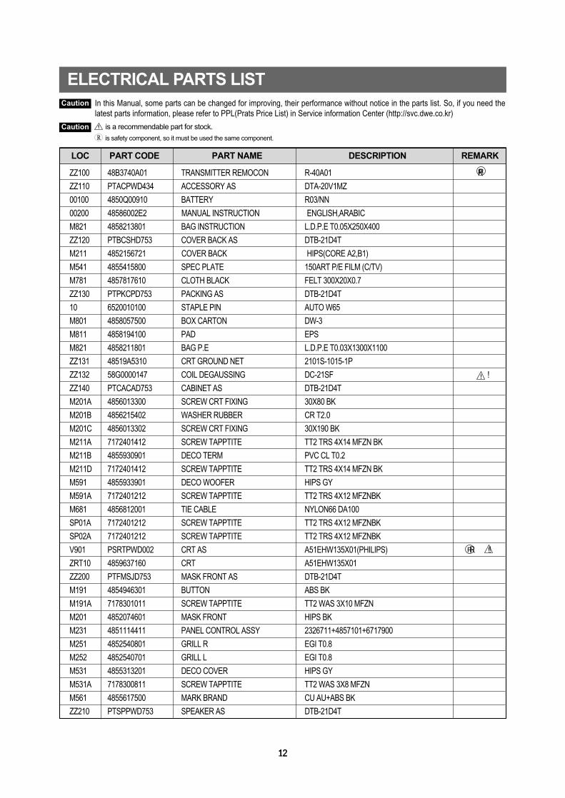
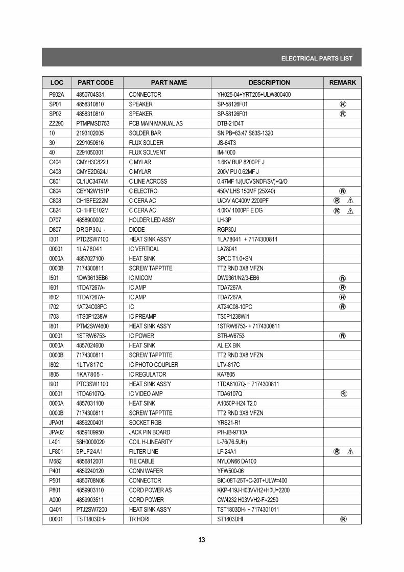
ELECTRICAL PARTS LIST
is a recommendable part for stock. is safety component, so it must be used the same component.
In this Manual, some parts can be changed for improving, their performance without notice in the parts list. So, if you need thelatest parts information, please refer to PPL(Prats Price List) in Service information Center (http://svc.dwe.co.kr)
Caution
Caution
1313
ELECTRICAL PARTS LIST
LOC PART CODE PART NAME DESCRIPTION REMARK
P602A 4850704S31 CONNECTOR YH025-04+YRT205+ULW800400
SP01 4858310810 SPEAKER SP-58126F01 R
SP02 4858310810 SPEAKER SP-58126F01 R
ZZ290 PTMPMSD753 PCB MAIN MANUAL AS DTB-21D4T
10 2193102005 SOLDER BAR SN:PB=63:47 S63S-1320
30 2291050616 FLUX SOLDER JS-64T3
40 2291050301 FLUX SOLVENT IM-1000
C404 CMYH3C822J C MYLAR 1.6KV BUP 8200PF J
C408 CMYE2D624J C MYLAR 200V PU 0.62MF J
C801 CL1UC3474M C LINE ACROSS 0.47MF 1J(UCVSNDF/SV)+Q/O
C804 CEYN2W151P C ELECTRO 450V LHS 150MF (25X40) R
C808 CH1BFE222M C CERA AC U/C/V AC400V 2200PF R !
C824 CH1HFE102M C CERA AC 4.0KV 1000PF E DG R !
D707 4858900002 HOLDER LED ASSY LH-3P
D807 DRGP30J - DIODE RGP30J
I301 PTD2SW7100 HEAT SINK ASS‘Y 1LA78041 + 7174300811
00001 1LA78041 IC VERTICAL LA78041
0000A 4857027100 HEAT SINK SPCC T1.0+SN
0000B 7174300811 SCREW TAPPTITE TT2 RND 3X8 MFZN
I501 1DW3613EB6 IC MICOM DW9361/N2/3-EB6 R
I601 1TDA7267A- IC AMP TDA7267A R
I602 1TDA7267A- IC AMP TDA7267A R
I702 1AT24C08PC IC AT24C08-10PC R
I703 1TS0P1238W IC PREAMP TS0P1238WI1
I801 PTM2SW4600 HEAT SINK ASS‘Y 1STRW6753- + 7174300811
00001 1STRW6753- IC POWER STR-W6753 R
0000A 4857024600 HEAT SINK AL EX B/K
0000B 7174300811 SCREW TAPPTITE TT2 RND 3X8 MFZN
I802 1LTV817C IC PHOTO COUPLER LTV-817C
I805 1KA7805 - IC REGULATOR KA7805
I901 PTC3SW1100 HEAT SINK ASS‘Y 1TDA6107Q- + 7174300811
00001 1TDA6107Q- IC VIDEO AMP TDA6107Q R
0000A 4857031100 HEAT SINK A1050P-H24 T2.0
0000B 7174300811 SCREW TAPPTITE TT2 RND 3X8 MFZN
JPA01 4859200401 SOCKET RGB YRS21-R1
JPA02 4859109950 JACK PIN BOARD PH-JB-9710A
L401 58H0000020 COIL H-LINEARITY L-76(76.5UH)
LF801 5PLF24A1 FILTER LINE LF-24A1 R !
M682 4856812001 TIE CABLE NYLON66 DA100
P401 4859240120 CONN WAFER YFW500-06
P501 4850708N08 CONNECTOR BIC-08T-25T+C-20T+ULW=400
P801 4859903110 CORD POWER AS KKP-419J-H03VVH2+H0U=2200
A000 4859903511 CORD POWER CW4232 H03VVH2-F=2250
Q401 PTJ2SW7200 HEAT SINK ASS‘Y TST1803DH- + 7174301011
00001 TST1803DH- TR HORI ST1803DHI R
1414
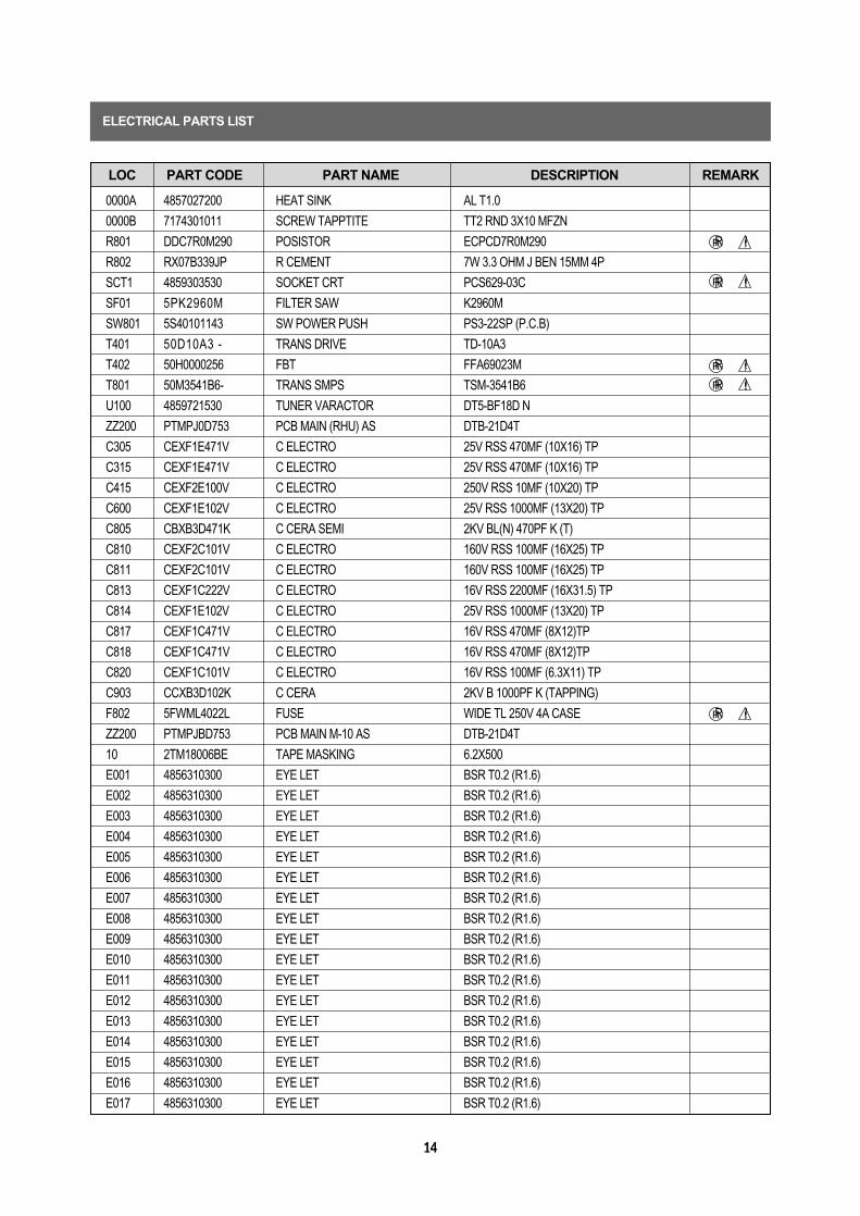
LOC PART CODE PART NAME DESCRIPTION REMARK
0000A 4857027200 HEAT SINK AL T1.0
0000B 7174301011 SCREW TAPPTITE TT2 RND 3X10 MFZN
R801 DDC7R0M290 POSISTOR ECPCD7R0M290 R !
R802 RX07B339JP R CEMENT 7W 3.3 OHM J BEN 15MM 4P
SCT1 4859303530 SOCKET CRT PCS629-03C R !
SF01 5PK2960M FILTER SAW K2960M
SW801 5S40101143 SW POWER PUSH PS3-22SP (P.C.B)
T401 50D10A3 - TRANS DRIVE TD-10A3
T402 50H0000256 FBT FFA69023M R !
T801 50M3541B6- TRANS SMPS TSM-3541B6 R !
U100 4859721530 TUNER VARACTOR DT5-BF18D N
ZZ200 PTMPJ0D753 PCB MAIN (RHU) AS DTB-21D4T
C305 CEXF1E471V C ELECTRO 25V RSS 470MF (10X16) TP
C315 CEXF1E471V C ELECTRO 25V RSS 470MF (10X16) TP
C415 CEXF2E100V C ELECTRO 250V RSS 10MF (10X20) TP
C600 CEXF1E102V C ELECTRO 25V RSS 1000MF (13X20) TP
C805 CBXB3D471K C CERA SEMI 2KV BL(N) 470PF K (T)
C810 CEXF2C101V C ELECTRO 160V RSS 100MF (16X25) TP
C811 CEXF2C101V C ELECTRO 160V RSS 100MF (16X25) TP
C813 CEXF1C222V C ELECTRO 16V RSS 2200MF (16X31.5) TP
C814 CEXF1E102V C ELECTRO 25V RSS 1000MF (13X20) TP
C817 CEXF1C471V C ELECTRO 16V RSS 470MF (8X12)TP
C818 CEXF1C471V C ELECTRO 16V RSS 470MF (8X12)TP
C820 CEXF1C101V C ELECTRO 16V RSS 100MF (6.3X11) TP
C903 CCXB3D102K C CERA 2KV B 1000PF K (TAPPING)
F802 5FWML4022L FUSE WIDE TL 250V 4A CASE R !
ZZ200 PTMPJBD753 PCB MAIN M-10 AS DTB-21D4T
10 2TM18006BE TAPE MASKING 6.2X500
E001 4856310300 EYE LET BSR T0.2 (R1.6)
E002 4856310300 EYE LET BSR T0.2 (R1.6)
E003 4856310300 EYE LET BSR T0.2 (R1.6)
E004 4856310300 EYE LET BSR T0.2 (R1.6)
E005 4856310300 EYE LET BSR T0.2 (R1.6)
E006 4856310300 EYE LET BSR T0.2 (R1.6)
E007 4856310300 EYE LET BSR T0.2 (R1.6)
E008 4856310300 EYE LET BSR T0.2 (R1.6)
E009 4856310300 EYE LET BSR T0.2 (R1.6)
E010 4856310300 EYE LET BSR T0.2 (R1.6)
E011 4856310300 EYE LET BSR T0.2 (R1.6)
E012 4856310300 EYE LET BSR T0.2 (R1.6)
E013 4856310300 EYE LET BSR T0.2 (R1.6)
E014 4856310300 EYE LET BSR T0.2 (R1.6)
E015 4856310300 EYE LET BSR T0.2 (R1.6)
E016 4856310300 EYE LET BSR T0.2 (R1.6)
E017 4856310300 EYE LET BSR T0.2 (R1.6)
ELECTRICAL PARTS LIST
1515
LOC PART CODE PART NAME DESCRIPTION REMARK
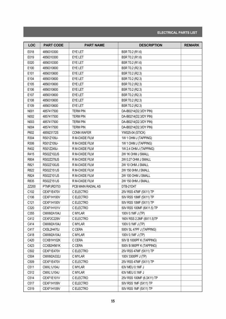
E018 4856310300 EYE LET BSR T0.2 (R1.6)
E019 4856310300 EYE LET BSR T0.2 (R1.6)
E020 4856310300 EYE LET BSR T0.2 (R1.6)
E100 4856310600 EYE LET BSR T0.2 (R2.3)
E101 4856310600 EYE LET BSR T0.2 (R2.3)
E104 4856310600 EYE LET BSR T0.2 (R2.3)
E105 4856310600 EYE LET BSR T0.2 (R2.3)
E106 4856310600 EYE LET BSR T0.2 (R2.3)
E107 4856310600 EYE LET BSR T0.2 (R2.3)
E108 4856310600 EYE LET BSR T0.2 (R2.3)
E109 4856310600 EYE LET BSR T0.2 (R2.3)
N001 4857417500 TERM PIN DA-IB0214(D2.3/DY PIN)
N002 4857417500 TERM PIN DA-IB0214(D2.3/DY PIN)
N003 4857417500 TERM PIN DA-IB0214(D2.3/DY PIN)
N004 4857417500 TERM PIN DA-IB0214(D2.3/DY PIN)
P602 485923172S CONN WAFER YW025-04 (STICK)
R304 RS01Z109J- R M-OXIDE FILM 1W 1 OHM J (TAPPING)
R306 RS01Z109J- R M-OXIDE FILM 1W 1 OHM J (TAPPING)
R402 RS01Z249J- R M-OXIDE FILM 1W 2.4 OHM J (TAPPING)
R415 RS02Z102JS R M-OXIDE FILM 2W 1K OHM J SMALL
R804 RS02Z278JS R M-OXIDE FILM 2W 0.27 OHM J SMALL
R821 RS02Z100JS R M-OXIDE FILM 2W 10 OHM J SMALL
R822 RS02Z151JS R M-OXIDE FILM 2W 150 0HM J SMALL
R824 RS02Z101JS R M-OXIDE FILM 2W 100 OHM J SMALL
R835 RS02Z151JS R M-OXIDE FILM 2W 150 0HM J SMALL
ZZ200 PTMPJRD753 PCB MAIN RADIAL AS DTB-21D4T
C102 CEXF1E470V C ELECTRO 25V RSS 47MF (5X11) TP
C106 CEXF1H100V C ELECTRO 50V RSS 10MF (5X11) TP
C121 CEXF1H100V C ELECTRO 50V RSS 10MF (5X11) TP
C320 CEXF1H101V C ELECTRO 50V RSS 100MF (8X11.5) TP
C355 CMXM2A104J C MYLAR 100V 0.1MF J (TP)
C412 CEXF2C229V C ELECTRO 160V RSS 2.2MF (8X11.5)TP
C414 CMXM2A104J C MYLAR 100V 0.1MF J (TP)
C417 CXSL2H470J C CERA 500V SL 47PF J (TAPPING)
C418 CMXM2A104J C MYLAR 100V 0.1MF J (TP)
C420 CCXB1H102K C CERA 50V B 1000PF K (TAPPING)
C423 CCXB2H561K C CERA 500V B 560PF K (TAPPING)
C502 CEXF1E470V C ELECTRO 25V RSS 47MF (5X11) TP
C504 CMXM2A332J C MYLAR 100V 3300PF J (TP)
C509 CEXF1E470V C ELECTRO 25V RSS 47MF (5X11) TP
C511 CMXL1J104J C MYLAR 63V MEU 0.1MF J
C512 CMXL1J104J C MYLAR 63V MEU 0.1MF J
C514 CEXF1E101V C ELECTRO 25V RSS 100MF (6.3X11) TP
C517 CEXF1H109V C ELECTRO 50V RSS 1MF (5X11) TP
C519 CEXF1H109V C ELECTRO 50V RSS 1MF (5X11) TP
ELECTRICAL PARTS LIST
1616
LOC PART CODE PART NAME DESCRIPTION REMARK
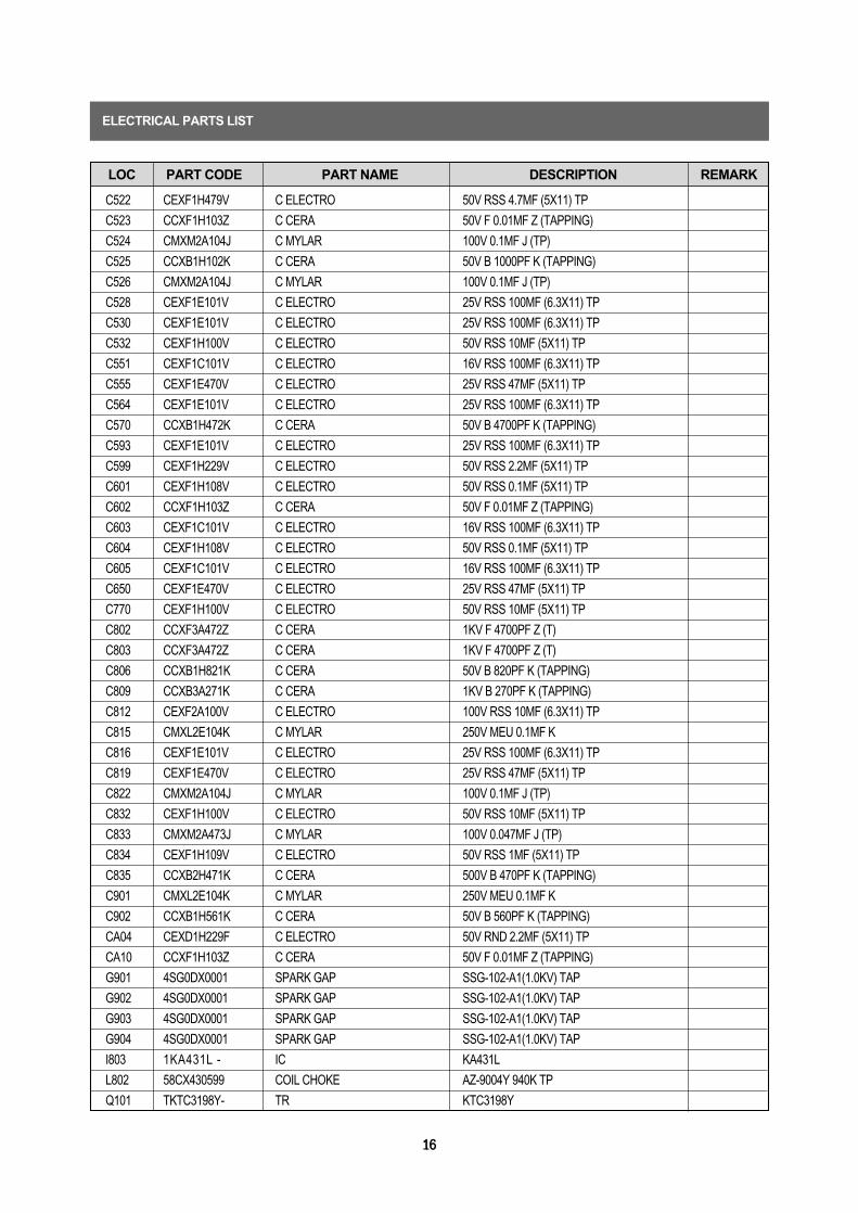
C522 CEXF1H479V C ELECTRO 50V RSS 4.7MF (5X11) TP
C523 CCXF1H103Z C CERA 50V F 0.01MF Z (TAPPING)
C524 CMXM2A104J C MYLAR 100V 0.1MF J (TP)
C525 CCXB1H102K C CERA 50V B 1000PF K (TAPPING)
C526 CMXM2A104J C MYLAR 100V 0.1MF J (TP)
C528 CEXF1E101V C ELECTRO 25V RSS 100MF (6.3X11) TP
C530 CEXF1E101V C ELECTRO 25V RSS 100MF (6.3X11) TP
C532 CEXF1H100V C ELECTRO 50V RSS 10MF (5X11) TP
C551 CEXF1C101V C ELECTRO 16V RSS 100MF (6.3X11) TP
C555 CEXF1E470V C ELECTRO 25V RSS 47MF (5X11) TP
C564 CEXF1E101V C ELECTRO 25V RSS 100MF (6.3X11) TP
C570 CCXB1H472K C CERA 50V B 4700PF K (TAPPING)
C593 CEXF1E101V C ELECTRO 25V RSS 100MF (6.3X11) TP
C599 CEXF1H229V C ELECTRO 50V RSS 2.2MF (5X11) TP
C601 CEXF1H108V C ELECTRO 50V RSS 0.1MF (5X11) TP
C602 CCXF1H103Z C CERA 50V F 0.01MF Z (TAPPING)
C603 CEXF1C101V C ELECTRO 16V RSS 100MF (6.3X11) TP
C604 CEXF1H108V C ELECTRO 50V RSS 0.1MF (5X11) TP
C605 CEXF1C101V C ELECTRO 16V RSS 100MF (6.3X11) TP
C650 CEXF1E470V C ELECTRO 25V RSS 47MF (5X11) TP
C770 CEXF1H100V C ELECTRO 50V RSS 10MF (5X11) TP
C802 CCXF3A472Z C CERA 1KV F 4700PF Z (T)
C803 CCXF3A472Z C CERA 1KV F 4700PF Z (T)
C806 CCXB1H821K C CERA 50V B 820PF K (TAPPING)
C809 CCXB3A271K C CERA 1KV B 270PF K (TAPPING)
C812 CEXF2A100V C ELECTRO 100V RSS 10MF (6.3X11) TP
C815 CMXL2E104K C MYLAR 250V MEU 0.1MF K
C816 CEXF1E101V C ELECTRO 25V RSS 100MF (6.3X11) TP
C819 CEXF1E470V C ELECTRO 25V RSS 47MF (5X11) TP
C822 CMXM2A104J C MYLAR 100V 0.1MF J (TP)
C832 CEXF1H100V C ELECTRO 50V RSS 10MF (5X11) TP
C833 CMXM2A473J C MYLAR 100V 0.047MF J (TP)
C834 CEXF1H109V C ELECTRO 50V RSS 1MF (5X11) TP
C835 CCXB2H471K C CERA 500V B 470PF K (TAPPING)
C901 CMXL2E104K C MYLAR 250V MEU 0.1MF K
C902 CCXB1H561K C CERA 50V B 560PF K (TAPPING)
CA04 CEXD1H229F C ELECTRO 50V RND 2.2MF (5X11) TP
CA10 CCXF1H103Z C CERA 50V F 0.01MF Z (TAPPING)
G901 4SG0DX0001 SPARK GAP SSG-102-A1(1.0KV) TAP
G902 4SG0DX0001 SPARK GAP SSG-102-A1(1.0KV) TAP
G903 4SG0DX0001 SPARK GAP SSG-102-A1(1.0KV) TAP
G904 4SG0DX0001 SPARK GAP SSG-102-A1(1.0KV) TAP
I803 1KA431L - IC KA431L
L802 58CX430599 COIL CHOKE AZ-9004Y 940K TP
Q101 TKTC3198Y- TR KTC3198Y
ELECTRICAL PARTS LIST
1717
LOC PART CODE PART NAME DESCRIPTION REMARK
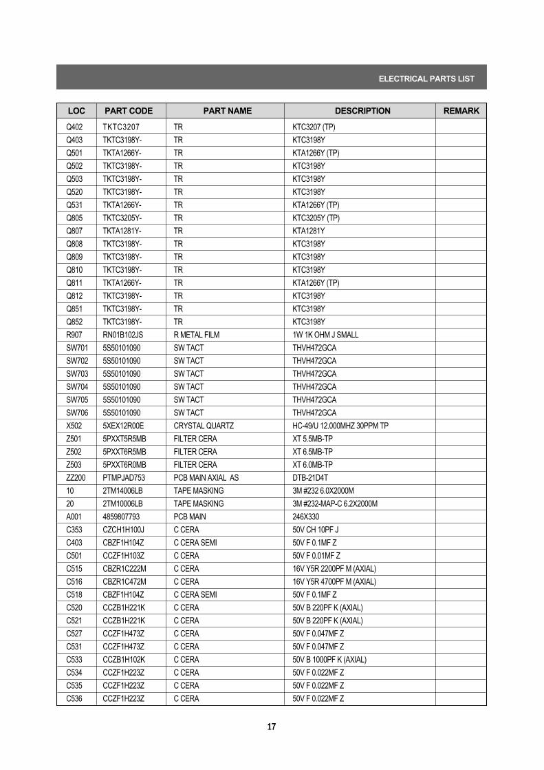
Q402 TKTC3207 TR KTC3207 (TP)
Q403 TKTC3198Y- TR KTC3198Y
Q501 TKTA1266Y- TR KTA1266Y (TP)
Q502 TKTC3198Y- TR KTC3198Y
Q503 TKTC3198Y- TR KTC3198Y
Q520 TKTC3198Y- TR KTC3198Y
Q531 TKTA1266Y- TR KTA1266Y (TP)
Q805 TKTC3205Y- TR KTC3205Y (TP)
Q807 TKTA1281Y- TR KTA1281Y
Q808 TKTC3198Y- TR KTC3198Y
Q809 TKTC3198Y- TR KTC3198Y
Q810 TKTC3198Y- TR KTC3198Y
Q811 TKTA1266Y- TR KTA1266Y (TP)
Q812 TKTC3198Y- TR KTC3198Y
Q851 TKTC3198Y- TR KTC3198Y
Q852 TKTC3198Y- TR KTC3198Y
R907 RN01B102JS R METAL FILM 1W 1K OHM J SMALL
SW701 5S50101090 SW TACT THVH472GCA
SW702 5S50101090 SW TACT THVH472GCA
SW703 5S50101090 SW TACT THVH472GCA
SW704 5S50101090 SW TACT THVH472GCA
SW705 5S50101090 SW TACT THVH472GCA
SW706 5S50101090 SW TACT THVH472GCA
X502 5XEX12R00E CRYSTAL QUARTZ HC-49/U 12.000MHZ 30PPM TP
Z501 5PXXT5R5MB FILTER CERA XT 5.5MB-TP
Z502 5PXXT6R5MB FILTER CERA XT 6.5MB-TP
Z503 5PXXT6R0MB FILTER CERA XT 6.0MB-TP
ZZ200 PTMPJAD753 PCB MAIN AXIAL AS DTB-21D4T
10 2TM14006LB TAPE MASKING 3M #232 6.0X2000M
20 2TM10006LB TAPE MASKING 3M #232-MAP-C 6.2X2000M
A001 4859807793 PCB MAIN 246X330
C353 CZCH1H100J C CERA 50V CH 10PF J
C403 CBZF1H104Z C CERA SEMI 50V F 0.1MF Z
C501 CCZF1H103Z C CERA 50V F 0.01MF Z
C515 CBZR1C222M C CERA 16V Y5R 2200PF M (AXIAL)
C516 CBZR1C472M C CERA 16V Y5R 4700PF M (AXIAL)
C518 CBZF1H104Z C CERA SEMI 50V F 0.1MF Z
C520 CCZB1H221K C CERA 50V B 220PF K (AXIAL)
C521 CCZB1H221K C CERA 50V B 220PF K (AXIAL)
C527 CCZF1H473Z C CERA 50V F 0.047MF Z
C531 CCZF1H473Z C CERA 50V F 0.047MF Z
C533 CCZB1H102K C CERA 50V B 1000PF K (AXIAL)
C534 CCZF1H223Z C CERA 50V F 0.022MF Z
C535 CCZF1H223Z C CERA 50V F 0.022MF Z
C536 CCZF1H223Z C CERA 50V F 0.022MF Z
ELECTRICAL PARTS LIST
1818
LOC PART CODE PART NAME DESCRIPTION REMARK
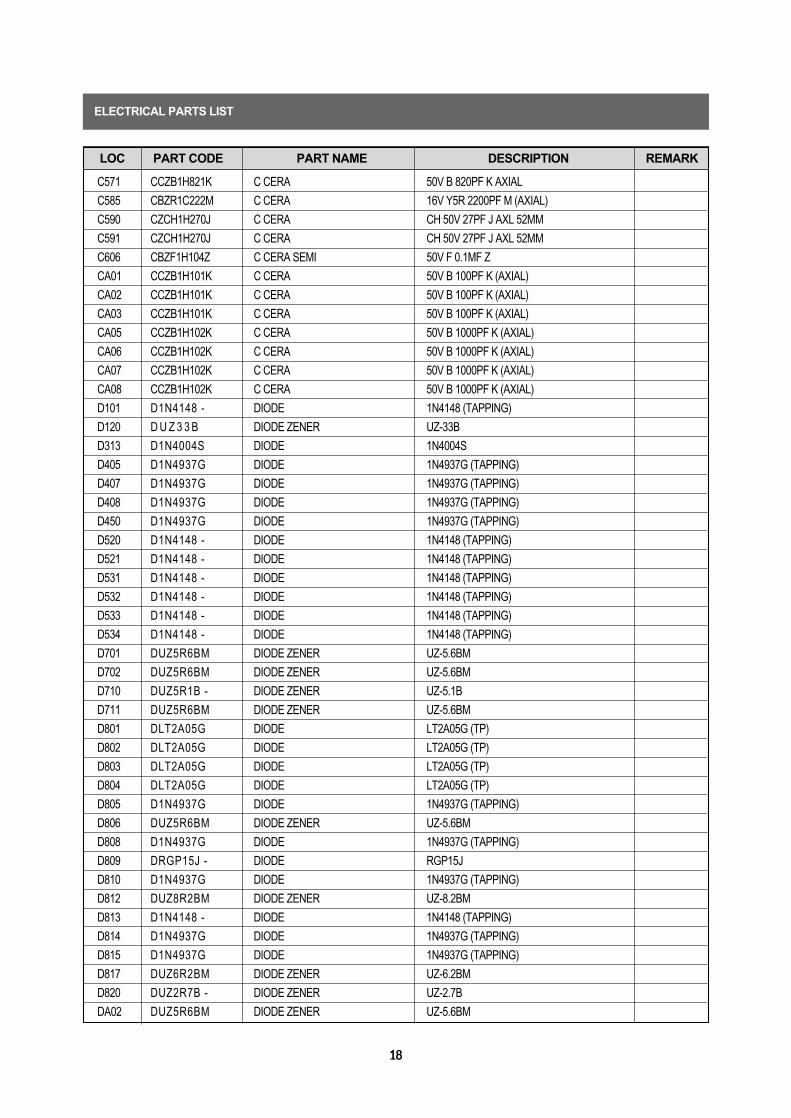
C571 CCZB1H821K C CERA 50V B 820PF K AXIAL
C585 CBZR1C222M C CERA 16V Y5R 2200PF M (AXIAL)
C590 CZCH1H270J C CERA CH 50V 27PF J AXL 52MM
C591 CZCH1H270J C CERA CH 50V 27PF J AXL 52MM
C606 CBZF1H104Z C CERA SEMI 50V F 0.1MF Z
CA01 CCZB1H101K C CERA 50V B 100PF K (AXIAL)
CA02 CCZB1H101K C CERA 50V B 100PF K (AXIAL)
CA03 CCZB1H101K C CERA 50V B 100PF K (AXIAL)
CA05 CCZB1H102K C CERA 50V B 1000PF K (AXIAL)
CA06 CCZB1H102K C CERA 50V B 1000PF K (AXIAL)
CA07 CCZB1H102K C CERA 50V B 1000PF K (AXIAL)
CA08 CCZB1H102K C CERA 50V B 1000PF K (AXIAL)
D101 D1N4148 - DIODE 1N4148 (TAPPING)
D120 D U Z 3 3 B DIODE ZENER UZ-33B
D313 D1N4004S DIODE 1N4004S
D405 D1N4937G DIODE 1N4937G (TAPPING)
D407 D1N4937G DIODE 1N4937G (TAPPING)
D408 D1N4937G DIODE 1N4937G (TAPPING)
D450 D1N4937G DIODE 1N4937G (TAPPING)
D520 D1N4148 - DIODE 1N4148 (TAPPING)
D521 D1N4148 - DIODE 1N4148 (TAPPING)
D531 D1N4148 - DIODE 1N4148 (TAPPING)
D532 D1N4148 - DIODE 1N4148 (TAPPING)
D533 D1N4148 - DIODE 1N4148 (TAPPING)
D534 D1N4148 - DIODE 1N4148 (TAPPING)
D701 DUZ5R6BM DIODE ZENER UZ-5.6BM
D702 DUZ5R6BM DIODE ZENER UZ-5.6BM
D710 DUZ5R1B - DIODE ZENER UZ-5.1B
D711 DUZ5R6BM DIODE ZENER UZ-5.6BM
D801 DLT2A05G DIODE LT2A05G (TP)
D802 DLT2A05G DIODE LT2A05G (TP)
D803 DLT2A05G DIODE LT2A05G (TP)
D804 DLT2A05G DIODE LT2A05G (TP)
D805 D1N4937G DIODE 1N4937G (TAPPING)
D806 DUZ5R6BM DIODE ZENER UZ-5.6BM
D808 D1N4937G DIODE 1N4937G (TAPPING)
D809 DRGP15J - DIODE RGP15J
D810 D1N4937G DIODE 1N4937G (TAPPING)
D812 DUZ8R2BM DIODE ZENER UZ-8.2BM
D813 D1N4148 - DIODE 1N4148 (TAPPING)
D814 D1N4937G DIODE 1N4937G (TAPPING)
D815 D1N4937G DIODE 1N4937G (TAPPING)
D817 DUZ6R2BM DIODE ZENER UZ-6.2BM
D820 DUZ2R7B - DIODE ZENER UZ-2.7B
DA02 DUZ5R6BM DIODE ZENER UZ-5.6BM
ELECTRICAL PARTS LIST
1919
LOC PART CODE PART NAME DESCRIPTION REMARK
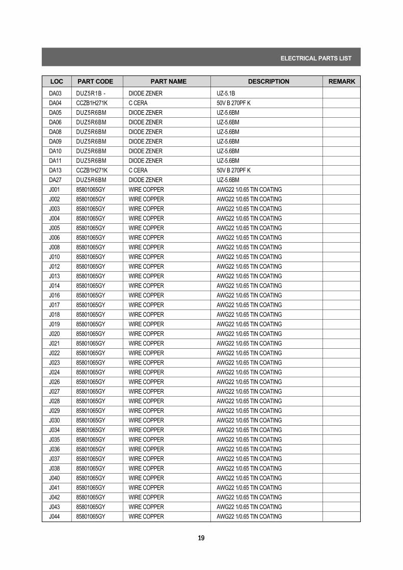
DA03 DUZ5R1B - DIODE ZENER UZ-5.1B
DA04 CCZB1H271K C CERA 50V B 270PF K
DA05 DUZ5R6BM DIODE ZENER UZ-5.6BM
DA06 DUZ5R6BM DIODE ZENER UZ-5.6BM
DA08 DUZ5R6BM DIODE ZENER UZ-5.6BM
DA09 DUZ5R6BM DIODE ZENER UZ-5.6BM
DA10 DUZ5R6BM DIODE ZENER UZ-5.6BM
DA11 DUZ5R6BM DIODE ZENER UZ-5.6BM
DA13 CCZB1H271K C CERA 50V B 270PF K
DA27 DUZ5R6BM DIODE ZENER UZ-5.6BM
J001 85801065GY WIRE COPPER AWG22 1/0.65 TIN COATING
J002 85801065GY WIRE COPPER AWG22 1/0.65 TIN COATING
J003 85801065GY WIRE COPPER AWG22 1/0.65 TIN COATING
J004 85801065GY WIRE COPPER AWG22 1/0.65 TIN COATING
J005 85801065GY WIRE COPPER AWG22 1/0.65 TIN COATING
J006 85801065GY WIRE COPPER AWG22 1/0.65 TIN COATING
J008 85801065GY WIRE COPPER AWG22 1/0.65 TIN COATING
J010 85801065GY WIRE COPPER AWG22 1/0.65 TIN COATING
J012 85801065GY WIRE COPPER AWG22 1/0.65 TIN COATING
J013 85801065GY WIRE COPPER AWG22 1/0.65 TIN COATING
J014 85801065GY WIRE COPPER AWG22 1/0.65 TIN COATING
J016 85801065GY WIRE COPPER AWG22 1/0.65 TIN COATING
J017 85801065GY WIRE COPPER AWG22 1/0.65 TIN COATING
J018 85801065GY WIRE COPPER AWG22 1/0.65 TIN COATING
J019 85801065GY WIRE COPPER AWG22 1/0.65 TIN COATING
J020 85801065GY WIRE COPPER AWG22 1/0.65 TIN COATING
J021 85801065GY WIRE COPPER AWG22 1/0.65 TIN COATING
J022 85801065GY WIRE COPPER AWG22 1/0.65 TIN COATING
J023 85801065GY WIRE COPPER AWG22 1/0.65 TIN COATING
J024 85801065GY WIRE COPPER AWG22 1/0.65 TIN COATING
J026 85801065GY WIRE COPPER AWG22 1/0.65 TIN COATING
J027 85801065GY WIRE COPPER AWG22 1/0.65 TIN COATING
J028 85801065GY WIRE COPPER AWG22 1/0.65 TIN COATING
J029 85801065GY WIRE COPPER AWG22 1/0.65 TIN COATING
J030 85801065GY WIRE COPPER AWG22 1/0.65 TIN COATING
J034 85801065GY WIRE COPPER AWG22 1/0.65 TIN COATING
J035 85801065GY WIRE COPPER AWG22 1/0.65 TIN COATING
J036 85801065GY WIRE COPPER AWG22 1/0.65 TIN COATING
J037 85801065GY WIRE COPPER AWG22 1/0.65 TIN COATING
J038 85801065GY WIRE COPPER AWG22 1/0.65 TIN COATING
J040 85801065GY WIRE COPPER AWG22 1/0.65 TIN COATING
J041 85801065GY WIRE COPPER AWG22 1/0.65 TIN COATING
J042 85801065GY WIRE COPPER AWG22 1/0.65 TIN COATING
J043 85801065GY WIRE COPPER AWG22 1/0.65 TIN COATING
J044 85801065GY WIRE COPPER AWG22 1/0.65 TIN COATING
ELECTRICAL PARTS LIST
2020
LOC PART CODE PART NAME DESCRIPTION REMARK
J045 85801065GY WIRE COPPER AWG22 1/0.65 TIN COATING
J050 85801065GY WIRE COPPER AWG22 1/0.65 TIN COATING
J052 85801065GY WIRE COPPER AWG22 1/0.65 TIN COATING
J053 85801065GY WIRE COPPER AWG22 1/0.65 TIN COATING
J054 85801065GY WIRE COPPER AWG22 1/0.65 TIN COATING
J055 85801065GY WIRE COPPER AWG22 1/0.65 TIN COATING
J056 85801065GY WIRE COPPER AWG22 1/0.65 TIN COATING
J057 85801065GY WIRE COPPER AWG22 1/0.65 TIN COATING
J059 85801065GY WIRE COPPER AWG22 1/0.65 TIN COATING
J060 85801065GY WIRE COPPER AWG22 1/0.65 TIN COATING
J061 85801065GY WIRE COPPER AWG22 1/0.65 TIN COATING
J062 85801065GY WIRE COPPER AWG22 1/0.65 TIN COATING
J065 85801065GY WIRE COPPER AWG22 1/0.65 TIN COATING
J067 85801065GY WIRE COPPER AWG22 1/0.65 TIN COATING
J068 85801065GY WIRE COPPER AWG22 1/0.65 TIN COATING
J069 85801065GY WIRE COPPER AWG22 1/0.65 TIN COATING
J070 85801065GY WIRE COPPER AWG22 1/0.65 TIN COATING
J071 85801065GY WIRE COPPER AWG22 1/0.65 TIN COATING
J072 85801065GY WIRE COPPER AWG22 1/0.65 TIN COATING
J073 85801065GY WIRE COPPER AWG22 1/0.65 TIN COATING
J074 85801065GY WIRE COPPER AWG22 1/0.65 TIN COATING
J075 85801065GY WIRE COPPER AWG22 1/0.65 TIN COATING
J076 85801065GY WIRE COPPER AWG22 1/0.65 TIN COATING
J077 85801065GY WIRE COPPER AWG22 1/0.65 TIN COATING
J078 85801065GY WIRE COPPER AWG22 1/0.65 TIN COATING
J079 85801065GY WIRE COPPER AWG22 1/0.65 TIN COATING
J080 85801065GY WIRE COPPER AWG22 1/0.65 TIN COATING
J081 85801065GY WIRE COPPER AWG22 1/0.65 TIN COATING
J082 85801065GY WIRE COPPER AWG22 1/0.65 TIN COATING
J083 85801065GY WIRE COPPER AWG22 1/0.65 TIN COATING
J084 85801065GY WIRE COPPER AWG22 1/0.65 TIN COATING
J085 85801065GY WIRE COPPER AWG22 1/0.65 TIN COATING
J086 85801065GY WIRE COPPER AWG22 1/0.65 TIN COATING
J087 85801065GY WIRE COPPER AWG22 1/0.65 TIN COATING
J088 85801065GY WIRE COPPER AWG22 1/0.65 TIN COATING
J089 85801065GY WIRE COPPER AWG22 1/0.65 TIN COATING
J090 85801065GY WIRE COPPER AWG22 1/0.65 TIN COATING
J092 85801065GY WIRE COPPER AWG22 1/0.65 TIN COATING
J094 85801065GY WIRE COPPER AWG22 1/0.65 TIN COATING
J095 85801065GY WIRE COPPER AWG22 1/0.65 TIN COATING
J096 85801065GY WIRE COPPER AWG22 1/0.65 TIN COATING
J097 85801065GY WIRE COPPER AWG22 1/0.65 TIN COATING
J098 85801065GY WIRE COPPER AWG22 1/0.65 TIN COATING
J099 85801065GY WIRE COPPER AWG22 1/0.65 TIN COATING
J100 85801065GY WIRE COPPER AWG22 1/0.65 TIN COATING
ELECTRICAL PARTS LIST
2121
LOC PART CODE PART NAME DESCRIPTION REMARK
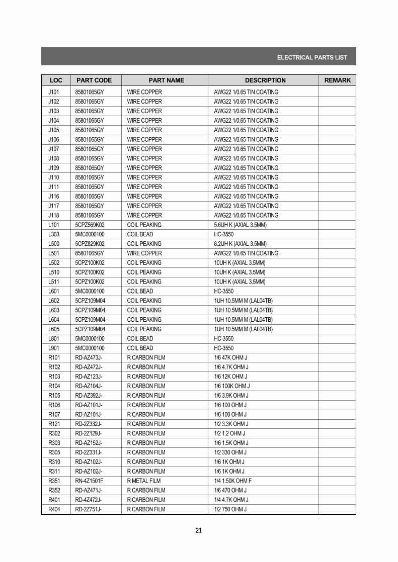
J101 85801065GY WIRE COPPER AWG22 1/0.65 TIN COATING
J102 85801065GY WIRE COPPER AWG22 1/0.65 TIN COATING
J103 85801065GY WIRE COPPER AWG22 1/0.65 TIN COATING
J104 85801065GY WIRE COPPER AWG22 1/0.65 TIN COATING
J105 85801065GY WIRE COPPER AWG22 1/0.65 TIN COATING
J106 85801065GY WIRE COPPER AWG22 1/0.65 TIN COATING
J107 85801065GY WIRE COPPER AWG22 1/0.65 TIN COATING
J108 85801065GY WIRE COPPER AWG22 1/0.65 TIN COATING
J109 85801065GY WIRE COPPER AWG22 1/0.65 TIN COATING
J110 85801065GY WIRE COPPER AWG22 1/0.65 TIN COATING
J111 85801065GY WIRE COPPER AWG22 1/0.65 TIN COATING
J116 85801065GY WIRE COPPER AWG22 1/0.65 TIN COATING
J117 85801065GY WIRE COPPER AWG22 1/0.65 TIN COATING
J118 85801065GY WIRE COPPER AWG22 1/0.65 TIN COATING
L101 5CPZ569K02 COIL PEAKING 5.6UH K (AXIAL 3.5MM)
L303 5MC0000100 COIL BEAD HC-3550
L500 5CPZ829K02 COIL PEAKING 8.2UH K (AXIAL 3.5MM)
L501 85801065GY WIRE COPPER AWG22 1/0.65 TIN COATING
L502 5CPZ100K02 COIL PEAKING 10UH K (AXIAL 3.5MM)
L510 5CPZ100K02 COIL PEAKING 10UH K (AXIAL 3.5MM)
L511 5CPZ100K02 COIL PEAKING 10UH K (AXIAL 3.5MM)
L601 5MC0000100 COIL BEAD HC-3550
L602 5CPZ109M04 COIL PEAKING 1UH 10.5MM M (LAL04TB)
L603 5CPZ109M04 COIL PEAKING 1UH 10.5MM M (LAL04TB)
L604 5CPZ109M04 COIL PEAKING 1UH 10.5MM M (LAL04TB)
L605 5CPZ109M04 COIL PEAKING 1UH 10.5MM M (LAL04TB)
L801 5MC0000100 COIL BEAD HC-3550
L901 5MC0000100 COIL BEAD HC-3550
R101 RD-AZ473J- R CARBON FILM 1/6 47K OHM J
R102 RD-AZ472J- R CARBON FILM 1/6 4.7K OHM J
R103 RD-AZ123J- R CARBON FILM 1/6 12K OHM J
R104 RD-AZ104J- R CARBON FILM 1/6 100K OHM J
R105 RD-AZ392J- R CARBON FILM 1/6 3.9K OHM J
R106 RD-AZ101J- R CARBON FILM 1/6 100 OHM J
R107 RD-AZ101J- R CARBON FILM 1/6 100 OHM J
R121 RD-2Z332J- R CARBON FILM 1/2 3.3K OHM J
R302 RD-2Z129J- R CARBON FILM 1/2 1.2 OHM J
R303 RD-AZ152J- R CARBON FILM 1/6 1.5K OHM J
R305 RD-2Z331J- R CARBON FILM 1/2 330 OHM J
R310 RD-AZ102J- R CARBON FILM 1/6 1K OHM J
R311 RD-AZ102J- R CARBON FILM 1/6 1K OHM J
R351 RN-4Z1501F R METAL FILM 1/4 1.50K OHM F
R352 RD-AZ471J- R CARBON FILM 1/6 470 OHM J
R401 RD-4Z472J- R CARBON FILM 1/4 4.7K OHM J
R404 RD-2Z751J- R CARBON FILM 1/2 750 OHM J
ELECTRICAL PARTS LIST
22
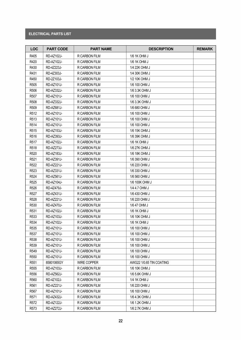
R405 RD-AZ102J- R CARBON FILM 1/6 1K OHM J
R420 RD-AZ102J- R CARBON FILM 1/6 1K OHM J
R430 RD-4Z223J- R CARBON FILM 1/4 22K OHM J
R431 RD-4Z303J- R CARBON FILM 1/4 30K OHM J
R450 RD-2Z103J- R CARBON FILM 1/2 10K OHM J
R505 RD-AZ101J- R CARBON FILM 1/6 100 OHM J
R506 RD-AZ332J- R CARBON FILM 1/6 3.3K OHM J
R507 RD-AZ101J- R CARBON FILM 1/6 100 OHM J
R508 RD-AZ332J- R CARBON FILM 1/6 3.3K OHM J
R509 RD-AZ681J- R CARBON FILM 1/6 680 OHM J
R512 RD-AZ101J- R CARBON FILM 1/6 100 OHM J
R513 RD-AZ101J- R CARBON FILM 1/6 100 OHM J
R514 RD-AZ101J- R CARBON FILM 1/6 100 OHM J
R515 RD-AZ153J- R CARBON FILM 1/6 15K OHM J
R516 RD-AZ393J- R CARBON FILM 1/6 39K OHM J
R517 RD-AZ102J- R CARBON FILM 1/6 1K OHM J
R518 RD-AZ273J- R CARBON FILM 1/6 27K OHM J
R520 RD-AZ183J- R CARBON FILM 1/6 18K OHM J
R521 RD-AZ391J- R CARBON FILM 1/6 390 OHM J
R522 RD-AZ221J- R CARBON FILM 1/6 220 OHM J
R523 RD-AZ331J- R CARBON FILM 1/6 330 OHM J
R524 RD-AZ561J- R CARBON FILM 1/6 560 OHM J
R525 RD-AZ104J- R CARBON FILM 1/6 100K OHM J
R526 RD-4Z479J- R CARBON FILM 1/4 4.7 OHM J
R527 RD-AZ431J- R CARBON FILM 1/6 430 OHM J
R528 RD-AZ221J- R CARBON FILM 1/6 220 OHM J
R530 RD-AZ470J- R CARBON FILM 1/6 47 OHM J
R531 RD-AZ102J- R CARBON FILM 1/6 1K OHM J
R533 RD-AZ103J- R CARBON FILM 1/6 10K OHM J
R534 RD-AZ102J- R CARBON FILM 1/6 1K OHM J
R535 RD-AZ101J- R CARBON FILM 1/6 100 OHM J
R537 RD-AZ101J- R CARBON FILM 1/6 100 OHM J
R538 RD-AZ101J- R CARBON FILM 1/6 100 OHM J
R539 RD-AZ101J- R CARBON FILM 1/6 100 OHM J
R549 RD-AZ101J- R CARBON FILM 1/6 100 OHM J
R550 RD-AZ101J- R CARBON FILM 1/6 100 OHM J
R551 85801065GY WIRE COPPER AWG22 1/0.65 TIN COATING
R555 RD-AZ103J- R CARBON FILM 1/6 10K OHM J
R556 RD-AZ562J- R CARBON FILM 1/6 5.6K OHM J
R560 RD-4Z102J- R CARBON FILM 1/4 1K OHM J
R561 RD-AZ221J- R CARBON FILM 1/6 220 OHM J
R567 RD-AZ101J- R CARBON FILM 1/6 100 OHM J
R571 RD-AZ432J- R CARBON FILM 1/6 4.3K OHM J
R572 RD-AZ122J- R CARBON FILM 1/6 1.2K OHM J
R573 RD-AZ272J- R CARBON FILM 1/6 2.7K OHM J
22
LOC PART CODE PART NAME DESCRIPTION REMARK
ELECTRICAL PARTS LIST
23
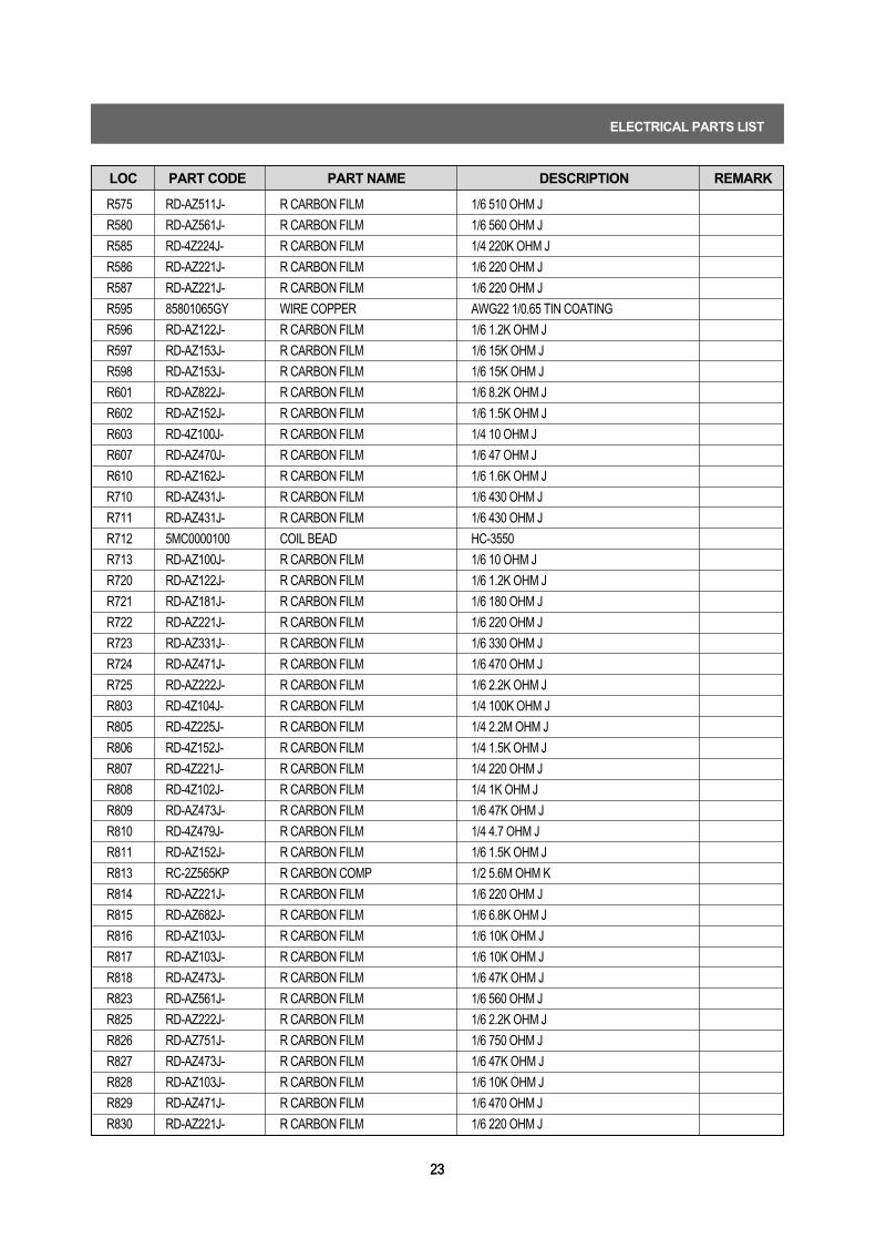
R575 RD-AZ511J- R CARBON FILM 1/6 510 OHM J
R580 RD-AZ561J- R CARBON FILM 1/6 560 OHM J
R585 RD-4Z224J- R CARBON FILM 1/4 220K OHM J
R586 RD-AZ221J- R CARBON FILM 1/6 220 OHM J
R587 RD-AZ221J- R CARBON FILM 1/6 220 OHM J
R595 85801065GY WIRE COPPER AWG22 1/0.65 TIN COATING
R596 RD-AZ122J- R CARBON FILM 1/6 1.2K OHM J
R597 RD-AZ153J- R CARBON FILM 1/6 15K OHM J
R598 RD-AZ153J- R CARBON FILM 1/6 15K OHM J
R601 RD-AZ822J- R CARBON FILM 1/6 8.2K OHM J
R602 RD-AZ152J- R CARBON FILM 1/6 1.5K OHM J
R603 RD-4Z100J- R CARBON FILM 1/4 10 OHM J
R607 RD-AZ470J- R CARBON FILM 1/6 47 OHM J
R610 RD-AZ162J- R CARBON FILM 1/6 1.6K OHM J
R710 RD-AZ431J- R CARBON FILM 1/6 430 OHM J
R711 RD-AZ431J- R CARBON FILM 1/6 430 OHM J
R712 5MC0000100 COIL BEAD HC-3550
R713 RD-AZ100J- R CARBON FILM 1/6 10 OHM J
R720 RD-AZ122J- R CARBON FILM 1/6 1.2K OHM J
R721 RD-AZ181J- R CARBON FILM 1/6 180 OHM J
R722 RD-AZ221J- R CARBON FILM 1/6 220 OHM J
R723 RD-AZ331J- R CARBON FILM 1/6 330 OHM J
R724 RD-AZ471J- R CARBON FILM 1/6 470 OHM J
R725 RD-AZ222J- R CARBON FILM 1/6 2.2K OHM J
R803 RD-4Z104J- R CARBON FILM 1/4 100K OHM J
R805 RD-4Z225J- R CARBON FILM 1/4 2.2M OHM J
R806 RD-4Z152J- R CARBON FILM 1/4 1.5K OHM J
R807 RD-4Z221J- R CARBON FILM 1/4 220 OHM J
R808 RD-4Z102J- R CARBON FILM 1/4 1K OHM J
R809 RD-AZ473J- R CARBON FILM 1/6 47K OHM J
R810 RD-4Z479J- R CARBON FILM 1/4 4.7 OHM J
R811 RD-AZ152J- R CARBON FILM 1/6 1.5K OHM J
R813 RC-2Z565KP R CARBON COMP 1/2 5.6M OHM K
R814 RD-AZ221J- R CARBON FILM 1/6 220 OHM J
R815 RD-AZ682J- R CARBON FILM 1/6 6.8K OHM J
R816 RD-AZ103J- R CARBON FILM 1/6 10K OHM J
R817 RD-AZ103J- R CARBON FILM 1/6 10K OHM J
R818 RD-AZ473J- R CARBON FILM 1/6 47K OHM J
R823 RD-AZ561J- R CARBON FILM 1/6 560 OHM J
R825 RD-AZ222J- R CARBON FILM 1/6 2.2K OHM J
R826 RD-AZ751J- R CARBON FILM 1/6 750 OHM J
R827 RD-AZ473J- R CARBON FILM 1/6 47K OHM J
R828 RD-AZ103J- R CARBON FILM 1/6 10K OHM J
R829 RD-AZ471J- R CARBON FILM 1/6 470 OHM J
R830 RD-AZ221J- R CARBON FILM 1/6 220 OHM J
LOC PART CODE PART NAME DESCRIPTION REMARK
23
ELECTRICAL PARTS LIST
2424
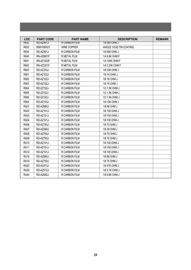
R831 RD-AZ473J- R CARBON FILM 1/6 47K OHM J
R832 RD-AZ561J- R CARBON FILM 1/6 560 OHM J
R833 85801065GY WIRE COPPER AWG22 1/0.65 TIN COATING
R834 RD-AZ561J- R CARBON FILM 1/6 560 OHM J
R840 RN-4Z6801F R METAL FILM 1/4 6.8K OHM F
R841 RN-4Z1003F R METAL FILM 1/4 100K OHM F
R842 RN-4Z2201F R METAL FILM 1/4 2.20K OHM F
R843 RD-AZ333J- R CARBON FILM 1/6 33K OHM J
R901 RD-AZ102J- R CARBON FILM 1/6 1K OHM J
R902 RD-AZ102J- R CARBON FILM 1/6 1K OHM J
R903 RD-AZ102J- R CARBON FILM 1/6 1K OHM J
R904 RD-2Z152J- R CARBON FILM 1/2 1.5K OHM J
R905 RD-2Z152J- R CARBON FILM 1/2 1.5K OHM J
R906 RD-2Z152J- R CARBON FILM 1/2 1.5K OHM J
R954 RD-AZ103J- R CARBON FILM 1/6 10K OHM J
RA01 RD-AZ680J- R CARBON FILM 1/6 68 OHM J
RA02 RD-AZ101J- R CARBON FILM 1/6 100 OHM J
RA03 RD-AZ101J- R CARBON FILM 1/6 100 OHM J
RA04 RD-AZ101J- R CARBON FILM 1/6 100 OHM J
RA06 RD-AZ750J- R CARBON FILM 1/6 75 OHM J
RA07 RD-AZ390J- R CARBON FILM 1/6 39 OHM J
RA08 RD-AZ750J- R CARBON FILM 1/6 75 OHM J
RA09 RD-AZ750J- R CARBON FILM 1/6 75 OHM J
RA10 RD-AZ101J- R CARBON FILM 1/6 100 OHM J
RA11 RD-AZ101J- R CARBON FILM 1/6 100 OHM J
RA12 RD-AZ101J- R CARBON FILM 1/6 100 OHM J
RA16 RD-AZ680J- R CARBON FILM 1/6 68 OHM J
RA19 RD-AZ750J- R CARBON FILM 1/6 75 OHM J
RA20 RD-AZ473J- R CARBON FILM 1/6 47K OHM J
RA30 RD-AZ512J- R CARBON FILM 1/6 5.1K OHM J
RA44 RD-AZ682J- R CARBON FILM 1/6 6.8K OHM J
LOC PART CODE PART NAME DESCRIPTION REMARK
11
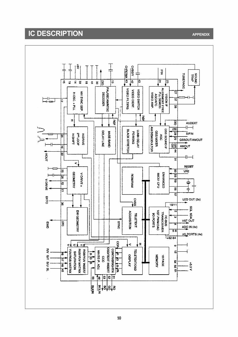
FUNCTIONAL DESCRIPTION OF VIDEO PROCESSOR Vision IF amplifier
The vision IF amplifier can demodulate signals with positive and negative modulation. The PLL demodulator is completely alignment-free.
The VCO of the PLL circuit is internal and the frequency is fixed to the required value by using the clock frequency of the-Controller/Teletext decoder as a reference. The setting of the various frequencies is made by the controlling software insubaddress 27H (33.9 MHz for system L-and 38.9 MHz for all other systems) Because of the internal VCO, the IF circuithas a high immunity to EMC interference.
1. IF demodulator and audio amplifier
The FM demodulator is realised as a narrow band PLL with external loop filter, which provides the necessary selectivitywithout using an extra band pass filter. To obtain good selectivity a linear phase detector and a constant input signalamplitude are required. For this reason the intercarrier signal is internally supplied to the demodulator via a gain controlledamplifier and AGC circuit. The nominal frequency of the demodulator is set via a gain controlled amplifier and AGC circuit.The nominal frequency of the demodulator is tuned to the required frequency (5.5 / 6.0 / 6.5 MHz) by means of acalibration circuit which uses the clock frequency of the microcontroller as a reference. Selection of the required frequencyis done by the controlling software.
Video switches
The video switch has one input for an external CVBS or Y/C signal. The selected CVBS signal can be supplied to pin 38,the IF video output. The selection between both signals is realised by the controlling software in subaddress 22H.
The video ident circuit is connected to the selected signal. This ident circuit is independent of the synchronisation.
Synchronisation circuit
The IC contains separator circuits for the horizontal and vertical sync pulses and a data-slicing circuit which extracts thedigital teletext data from the analogue signal.
The horizontal drive signal is obtained from an internal VCO which is running at a frequency of 25 MHz. This oscillator isstabilised to this frequency by using a 12 MHz signal coming from the reference oscillator of the -Controller/Teletextdecoder.
The horizontal drive is switched on and off via the soft start/stop procedure. This function is realised by means of variationof the TON of the horizontal drive pulses.
FUNCTIONAL DESCRIPTION For CP-185L/G
APPENDIX
22
The vertical synchronisation is realised by means of a divider circuit. The vertical ramp generator needs an externalresistor and capacitor. For the vertical drive a differential output current is available. The outputs are DC coupled to thevertical output stage.
The following geometry parameters can be adjusted:¥ Horizontal shift¥ Vertical amplitude¥ Vertical slope¥ S-correction¥ Vertical shift
Chroma and luminance processing
The chroma band-pass and trap circuits (including the SECAM cloche filter) are realised by means of gyrators and aretuned to the right frequency by comparing the tuning frequency with the reference frequency of the colour decoder. Theluminance delay line and the delay cells for the peaking circuit are also realised with gyrators. The circuit contains a blackstretcher functi on which corrects the black level for incoming signals which have a difference between the black level andthe blanking level.
Colour decoder
The ICs can decode PAL, NTSC and SECAM signals. The PAL/NTSC decoder does not need external referencecrystals but has an internal clock generator which is stabilised to the required frequency by using the 12 MHz clock signalfrom the referenc oscillator of the -Controller/Teletext decoder.
The Automatic Colour Limiting (ACL) circuit (switchable via the ACL bit in subaddress 2OH) prevents oversaturationoccurring when signals with a high chroma-to-burst ratio are received. The ACL circuit is designed such that it onlyreduces the chroma signal and not the burst signal. This has the advantage that the colour sensitivity is not affected bythis function.
SOFTWARE CONTROL
The CPU communicates with the peripheral functions using Special function Registers (SFRS) which are addressed asRAM locations. The registers for the Teletext decoder appear as normal SFRs in the -Controller memory map and arewritten to these functions by using a serial bus. This bus is controlled by dedicated hardware which uses a simplehandshake system for software synchronisation.
For compatibility reasons and possible re-use of software blocks, the TV processor is controlled by I2C bus. The TVprocessor control registers cannot be read. Only the status registers can be read ( Read address 8A ).
The SECAM decoder contains an auto-calibrating PLL demodulator which has two references, via the divided 12 MHzreference frequency (obtained from the -Controller) which is used to tune the PLL to the desired free-running frequencyand the bandgap reference to obtain the correct absolute value of the output signal. The VCO of the PLL is calibratedduring each vertical blanking period, when the IC is in search or SECAM mode.
The base-band delay line (TDA 4665 function) is integrated. This delay line is also active during NTSC reception, toobtain a good suppression of cross colour effects. The demodulated colour difference signals are internally supplied tothe delay line.
2
FUNCTIONAL DESCRIPTION APPENDIX
33
RGB output circuit and black-current stabilization
In the RGB control circuit the signal is controlled on contrast, brightness and saturation. The ICs have a linear input forexternal RGB signals. The signals for OSD and text are internally supplied to the control circuit. The output signal has anamplitude of about 2 Volts black-to-white at nominal input signals and nominal settings of the various controls.
To obtain an accurate biasing of the picture tube the ’Continuous Cathode Calibration’ system has been included in theseICs. A black level off set can be made with respect to the level which is generated by the black current stabilisationsystem. In this way different colour temperatures can be obtained for the bright and the dark part of the picture.The black current stabilisation system checks the output level of the 3 channels and indicates whether the black level ofthe highest output is in a certain window or below or above this window. This indication is read from the status byte 01and is used for automatic adjustment of the Vg2d voltage during the production of the TV receiver.
During switch-off of the TV receiver a fixed beam current is generated by the black current control circuit. This currentensures that the picture tube capacitance is discharged. During the switch-off period the vertical deflection is placed in anoverscan position so that the discharge is not visible on the screen.
2. IF
The TDA9361/TDA9381 has an alignment free IF PLL demodulator. The fully integrated oscillator is automaticallycalibrated, using the 12 MHz crystal as a frequency reference. The IF frequency is simply set in TV-Processor by I2C bus.The AFC information is available via I2C bus from the TV-Processor status bytes. The controlling software uses thisinformation for tuner frequency tracking ( automatic following ). The AFC window is typically 125Khz wide. The minimumfrequency step of the tuner is 62.5 kHz.This AFC function is disabled when a program is tuned using the direct frequency entry or after fine tuning adjustment.Therefore it is recommended to tune a channel with the TV search function ( manual or ATSS ) or by using the directchannel entry to enable the Automatic Frequency Control.
3
FUNCTIONAL DESCRIPTION APPENDIX
44
For SECAM L and L’ the TDA9361/TDA9381 is switched to positive modulation via I2C bus. SECAM L’ transmission onlyoccur in VHF band I and have their picture and sound carrier interchanged, compared to SECAM L and PAL B/Gchannels. For SECAM’L the picture carrier is situated at 33.9 MHz and the AM sound carrier at 40.40 MHz. The IF PLLreference is tuned from 38.9 to 33.9 MHz, this is done via I2C Bus and the SIF filter is switched from channel 2 to channel1;this is done by pin 4 of TDA 9361.
The tuner AGC time constant is slower for positive than for negative modulation, because the TDA9361 reduces its AGCcurrent. To make the AGC time constant even slower an extra series resistor R103 is added. To prevent IF overloadwhen jumping from a very strong transmitter to a weak transmitter a diode D101 has been added
3. Source switching
Video :The TDA9361/TDA9381 has only one external video input. The SCART video in pin (#20) is connected to the frontRCA video input.
The controlling software via I2C bus selects the signal source :- Video signal from tuner ( Pin 40 ).- External video.- External SVHS from SCART.
The sound source switching is done in the video processor part and in the AM demodulator by the -Controller via I2Cbus.The video processor pin 28 has multiple functions and provides in this applicationbus.
- Deemphasis time constant- Audio monitor output- External AM input- Deemphasis time constant : The time constant is given by the capacitor C504,needer to obtain the 54 s time timeconstant for standarad PAL signal.
- Audio monitor output : the nominal output signal is 500 mVrms, for all standards. The signal is also internallyconnected through to the audio switch. This signal is not controlled by the volume setting and can be used forSCART audio output.
The signal is buffered to avoid influencing the deemphasis time constant and to adjust the output level.- External AM input : By software the deemphasis pin can be converted into an input pin. External AM signal forSECAM L/L’ is directly connected to this pin. In this configuration the FM sound is internally muted, DC levelremains at 3Vdc.
An external sound signal of 500mVrms is applied to pin 35 via a coupling capacitor. The input impedance of this pin is25k‰ typical. Switching between internal FM, external AM or external audio from SCART is controlled internally bysoftware.
4
FUNCTIONAL DESCRIPTION APPENDIX
The SAW filter ( SF1 ) has a double Nyquist slope at 38.9 MHz and 33.9 MHz needed for this multistandardapplication. The disadvantage of this choice is that a 5.5 MHz trap filter ( Z501 ) is needed to suppress the residualsound carrier in the video for B/G signals.
55
Fast R, G, B insertion : The external R, G, B insertion needs a fast switching and cannot be controlled by the software(instruction cycle of 1 sec). The fast switching pin 16 of SCART is directly connected to the TV processor pin 45 ( Fastblanking input ). The display is synchronised with the selected video source, i.e. to get stable R, G, B signal insertion theymust be synchronised with the selected video source.
4. µ-Controller I/O pin configuration and function
The I/O pins of the -Controller can be configured in many ways. All port functions can be individually programmed by thecontrolling software.Each I/O port pin can be individually programmed in these configurations :
Open drain
In this mode, the port can function as input and output. It requires an external pull-up resistor. The maximum allowablesupply voltage for this pull up resistor is +5V.So in this mode it is possible to interface a 5 Volt environment like I2C while the -Controller has a 3.3 Volt supply.
Push-Pull
The push pull mode can be used for output only. Both sinking and sourcing is active, which leads to steep slopes. Thelevels are 0 and Vddp, the supply voltage 3.3Volts.
High impedance
This mode can be used for input only operation of the port.
Special port for LED
Pin 10 and 11 have the same functionality as the general I/O pins but in addition, their current source and sink capacity is8 mA instead of 4 mA. These pins are used for driving LED’s via a series current limiting resistor.
µ-Controller I/O pin configuration and function table
5
FUNCTIONAL DESCRIPTION APPENDIX
pin nameconfiguration
descriptionStand by TV on
1 n.u. High impedance High impedance not used
2 SCL Open Drain Open Drain Serial clock line
3 SDA Open Drain Open Drain Serial data line
4 SECAM L’ High impedancePush Pull / High SIF filter switching + AM/FM impedance switching
5 OCP High impedance High impedanceOver Current Protection (Switch the set OFF if the voltage on this pin is <2.3V )
6 RF AGC in High impedance High impedanceUsed during ATSS to measure7RF signal level.
7 Key in High impedance High impedance Local keyboard input
8 S/SW High impedance High impedance external video switch
10 Red LED High impedance Open Drain
11 Green LED Open Drain High impedance
62 Audio mute Push Pull High impedance
66
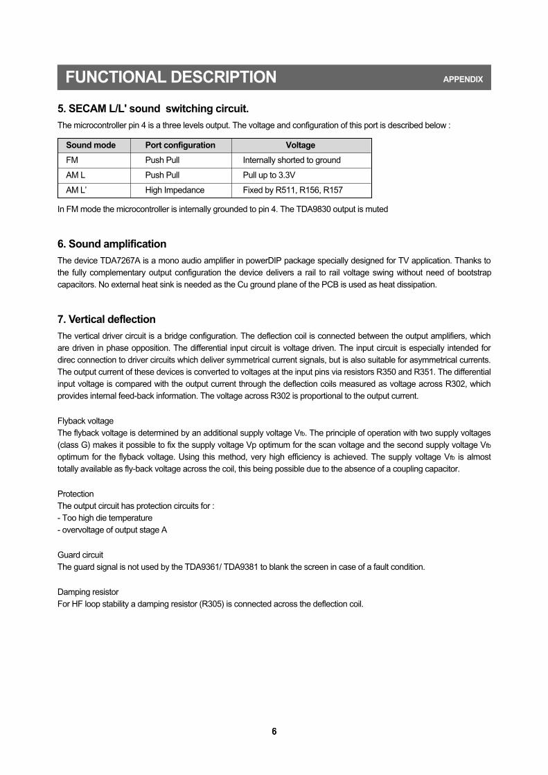
5. SECAM L/L' sound switching circuit.
The microcontroller pin 4 is a three levels output. The voltage and configuration of this port is described below :
In FM mode the microcontroller is internally grounded to pin 4. The TDA9830 output is muted
6. Sound amplification
The device TDA7267A is a mono audio amplifier in powerDIP package specially designed for TV application. Thanks tothe fully complementary output configuration the device delivers a rail to rail voltage swing without need of bootstrapcapacitors. No external heat sink is needed as the Cu ground plane of the PCB is used as heat dissipation.
7. Vertical deflection
The vertical driver circuit is a bridge configuration. The deflection coil is connected between the output amplifiers, whichare driven in phase opposition. The differential input circuit is voltage driven. The input circuit is especially intended fordirec connection to driver circuits which deliver symmetrical current signals, but is also suitable for asymmetrical currents.The output current of these devices is converted to voltages at the input pins via resistors R350 and R351. The differentialinput voltage is compared with the output current through the deflection coils measured as voltage across R302, whichprovides internal feed-back information. The voltage across R302 is proportional to the output current.
Flyback voltageThe flyback voltage is determined by an additional supply voltage Vfb. The principle of operation with two supply voltages(class G) makes it possible to fix the supply voltage Vp optimum for the scan voltage and the second supply voltage Vfb
optimum for the flyback voltage. Using this method, very high efficiency is achieved. The supply voltage Vfb is almosttotally available as fly-back voltage across the coil, this being possible due to the absence of a coupling capacitor.
ProtectionThe output circuit has protection circuits for :- Too high die temperature- overvoltage of output stage A
Guard circuitThe guard signal is not used by the TDA9361/ TDA9381 to blank the screen in case of a fault condition.
Damping resistor For HF loop stability a damping resistor (R305) is connected across the deflection coil.
6
FUNCTIONAL DESCRIPTION APPENDIX
Sound mode Port configuration Voltage
FM Push Pull Internally shorted to ground
AM L Push Pull Pull up to 3.3V
AM L’ High Impedance Fixed by R511, R156, R157
77
1. TDA9361 : TV signal processor - Teletext decoder with embedded µ-Controller.TDA9381 : TV signal processor - with embedded µ-Controller.
TV-signal Processor
¥ Multi-standard vision IF circuit with alignment-free PLL demodulator¥ Internal (switchable) time-constant for the IF-AGC circuit¥ Mono intercarrier with a selective FM-PLL demodulator which can be switched to the different FM sound frequencies
(5.5 / 6.0 / 6.5 MHz) ¥ Source selection between ’Internal’ CVBS and external CVBS or Y/C signals¥ Integrated chrominance trap circuit¥ Integrated luminance delay line with adjustable delay time¥ Asymmetrical’delay line type’ peaking in the luminance channel¥ Black stretching for non-standard luminance signals¥ lntegrated chroma band-pass filter with switchable centre frequency¥ Only one reference (12 MHz) crystal required for the -Controller, Teletext and the colour decoder¥ PAL / NTSC or multistandard colour decoder with automatic search system¥ Internal base-band delay line¥ RGB control circuit with ’Continuous Cathode Calibration’, white point and black level off set adjustment so that the
colour temperature of the dark and the bright parts of the screen can be chosen independently. ¥ Linear RGB or YUV input with fast blanking for external RGB/YUV sources. The Text/OSD signals are internally
supplied from the -Controller/Teletext decode¥ Contrast reduction possibility during mixed-mode of OSD and Text signals¥ Horizontal synchronisation with two control loops and alignment-free horizontal oscillator¥ Vertical count-down circuit¥ Vertical driver optimised for DC-coupled vertical output stages¥ Horizontal and vertical geometry processing
µ-Controller
¥ 80C51 -controller core standard instruction set and timing¥ 1 s machine cycle¥ 64Kx8-bit programmed ROM¥ 3 - 12Kx8-bit Auxiliary RAM (shared with Display and Acquisition)¥ Interrupt controller for individual enable/disable with two level priority¥ Two 16-bit Timer/Counter registers¥ watchdog timer¥ Auxiliary RAM page pointer¥16-bit Data pointer¥ IDLE and Power Down (PD) mode¥ 8-bit A/D converter¥ 4 pins which can be programmed as general I/0 pin or ADC input.
7
IC DESCRIPTION APPENDIX
88
Data Capture
¥ Text memory 10 pages¥ Inventory of transmitted Teletext pages stored in the Transmitted Page Table (TPT) and Subtitle Page Table (SPT)¥ Data Capture for 525/625 line WST, VPS (PDC system A) and Wide Screen Signalling (WSS) bit decoding Automatic
selection between 525 WST/625 WST ¥ Automatic selection between 625 WST/VPS on line 16 of VBI¥ Real-time capture and decoding for WST Teletext in Hardware, to enable optimised -processor throughput ¥ Automatic detection of FASTEXT transmission¥ Real-time packet 26 engine in Hardware for processing accented, G2 and G3 characters¥ Signal quality detector for video and WST/VPS data types¥ Comprehensive teletext language coverage¥ Full Field and Vertical Blanking lnterval (VBI) data capture of WST data
Display
¥ Teletext and Enhanced OSD modes¥ Features of lever 1.5 WST.¥ Serial and Parallel Display Attributes¥ Single/Double/Quadruple Width and Height for characters¥ Scrolling of display region¥ Variable flash rate controlled by software¥ Enhanced display features including overlining, underlining and italics¥ Soft colours using CLUT with 4096 colour palette¥ Globally selectable scan lines per row (9/10/13/16) and character matrix [12x10, 12xl3, 12x16 (VxH)]¥ Fringing (Shadow) selectable from N-S-E-W direction¥ Fringe colour selectable¥ Meshing of defined area¥ Contrast reduction of defined area¥ Cursor¥ Special Graphics Characters with two planes, allowing four colours per character¥ 32 software redefinable On-Screen display characters¥ 4 WST Character sets (GO/G2) in single device (e.g. Latin, Cyrillic, Greek, Arabic)¥ G1 Mosaic graphics, Limited G3 Line drawing characters¥ WST Character sets and Closed Caption Character set in single device
Data Capture
The Data Capture section takes in the analogue Composite Video and Blanking Signal (CVBS), and from this extracts therequired data, which is then decoded and stored in memory. The extraction of the data is performed in the digital domain. The first stage is to convert the analogue CVBS signal into adigital form. This is done using an ADC sampling at 12MHz. The data and clock recovery is then performed by a Multi-Rate Video Input Processor (MuIVIP). From the recovered data and clock the following data types are extracted WSTTeletext (625/525), Closed Caption, VPS, WSS. The extracted data is stored in either memory (DRAM) via the MemoryInterface or in SFR locations.
8
IC DESCRIPTION APPENDIX
99
Data Capture Features
- Video Signal Quality detector- Data Capture for 625 line WST - Data Capture for 525 line WST - Data Capture for US Closed Caption - Data Capture for VPS data (PDC system A) - Data Capture for Wide Screen Signalling (WSS) bit decoding - Automatic selection between 525 WST/625WST - Automatic selection between 625WST/VPS on line 16 of VBI - Real-time capture and decoding for WST Teletext in Hardware, to enable optimised microprocessor throughput - 10 pages stored On-Chip - lnventory of transmitted Teletext pages stored in the Transmitted Page Table (TPT) and Subtitle Page Table (SPT) - Automatic detection of FASTEXT transmission - Real-time packet 26 engine in Hardware for processing accented, G2 and G3 characters - Signal quality detector for WST/VPS data types - Comprehensive Teletext language coverage - Full Field and Vertical Blanking Interval (VBI) data capture of WST data
9
IC DESCRIPTION APPENDIX
101010
IC DESCRIPTION APPENDIX
1111
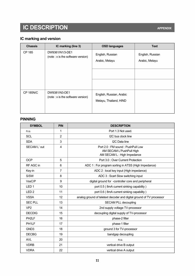
IC marking and version
11
PINNING
IC DESCRIPTION APPENDIX
Chassis IC marking (line 3) OSD languages Text
CP 185 DW9361/N1/3-DE1(note : x is the software version)
CP 185N/C DW9381/N3-DE1(note : x is the software version)
SYMBOL PIN DESCRIPTION
n.u. 1 Port 1.3 Not used.
SCL 2 I2C bus clock line
SDA 3 I2C Data line
SECAM L’ out 4 Port 2.0 : FM sound : PushPull LowAM SECAM L’PushPull High
AM SECAM L : High Impedance
OCP 5 Port 3.0 : Over Current Protection
RF AGC in 6 ADC 1 : For program sorting in ATSS (High Impedance)
Key-in 7 ADC 2 : local key input (High impedance)
S/SW 8 ADC 3 : Scart Slow switching input
VssC/P 9 digital ground for -controller core and peripheral
LED 1 10 port 0.5 ( 8mA current sinking capability )
LED 2 11 port 0.6 ( 8mA current sinking capability )
VSSA 12 analog ground of teletext decoder and digital ground of TV processor
SEC PLL 13 SECAM PLL decoupling
VP2 14 2nd supply voltage TV-processor
DECDIG 15 decoupling digital supply of TV-processor
PH2LF 16 phase-2 filter
PH1LF 17 phase-1 filter
GND3 18 ground 3 for TV-processor
DECBG 19 bandgap decoupling
AVL 20 n.u.
VDRB 21 vertical drive B output
VDRA 22 vertical drive A output
English, Russian
Arabic, Melayu
English, Russian, Arabic
Melayu, Thailand, HIND
English, Russian
Arabic, Melayu
1212
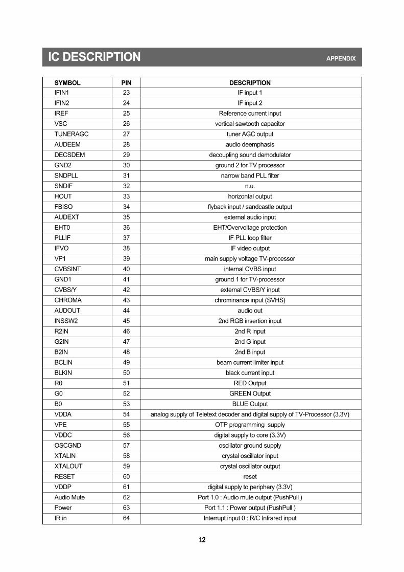
SYMBOL PIN DESCRIPTION
IFIN1 23 IF input 1
IFIN2 24 IF input 2
IREF 25 Reference current input
VSC 26 vertical sawtooth capacitor
TUNERAGC 27 tuner AGC output
AUDEEM 28 audio deemphasis
DECSDEM 29 decoupling sound demodulator
GND2 30 ground 2 for TV processor
SNDPLL 31 narrow band PLL filter
SNDIF 32 n.u.
HOUT 33 horizontal output
FBISO 34 flyback input / sandcastle output
AUDEXT 35 external audio input
EHT0 36 EHT/Overvoltage protection
PLLIF 37 IF PLL loop filter
IFVO 38 IF video output
VP1 39 main supply voltage TV-processor
CVBSINT 40 internal CVBS input
GND1 41 ground 1 for TV-processor
CVBS/Y 42 external CVBS/Y input
CHROMA 43 chrominance input (SVHS)
AUDOUT 44 audio out
INSSW2 45 2nd RGB insertion input
R2IN 46 2nd R input
G2IN 47 2nd G input
B2IN 48 2nd B input
BCLIN 49 beam current limiter input
BLKIN 50 black current input
R0 51 RED Output
G0 52 GREEN Output
B0 53 BLUE Output
VDDA 54 analog supply of Teletext decoder and digital supply of TV-Processor (3.3V)
VPE 55 OTP programming supply
VDDC 56 digital supply to core (3.3V)
OSCGND 57 oscillator ground supply
XTALIN 58 crystal oscillator input
XTALOUT 59 crystal oscillator output
RESET 60 reset
VDDP 61 digital supply to periphery (3.3V)
Audio Mute 62 Port 1.0 : Audio mute output (PushPull )
Power 63 Port 1.1 : Power output (PushPull )
IR in 64 Interrupt input 0 : R/C Infrared input
12
IC DESCRIPTION APPENDIX
131313
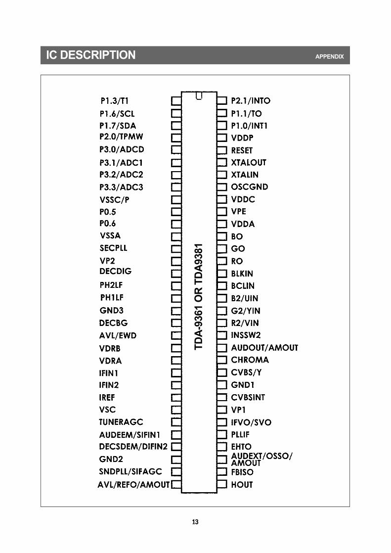
IC DESCRIPTION APPENDIX
TD
A-9
361
OR
TD
A93
81
1414
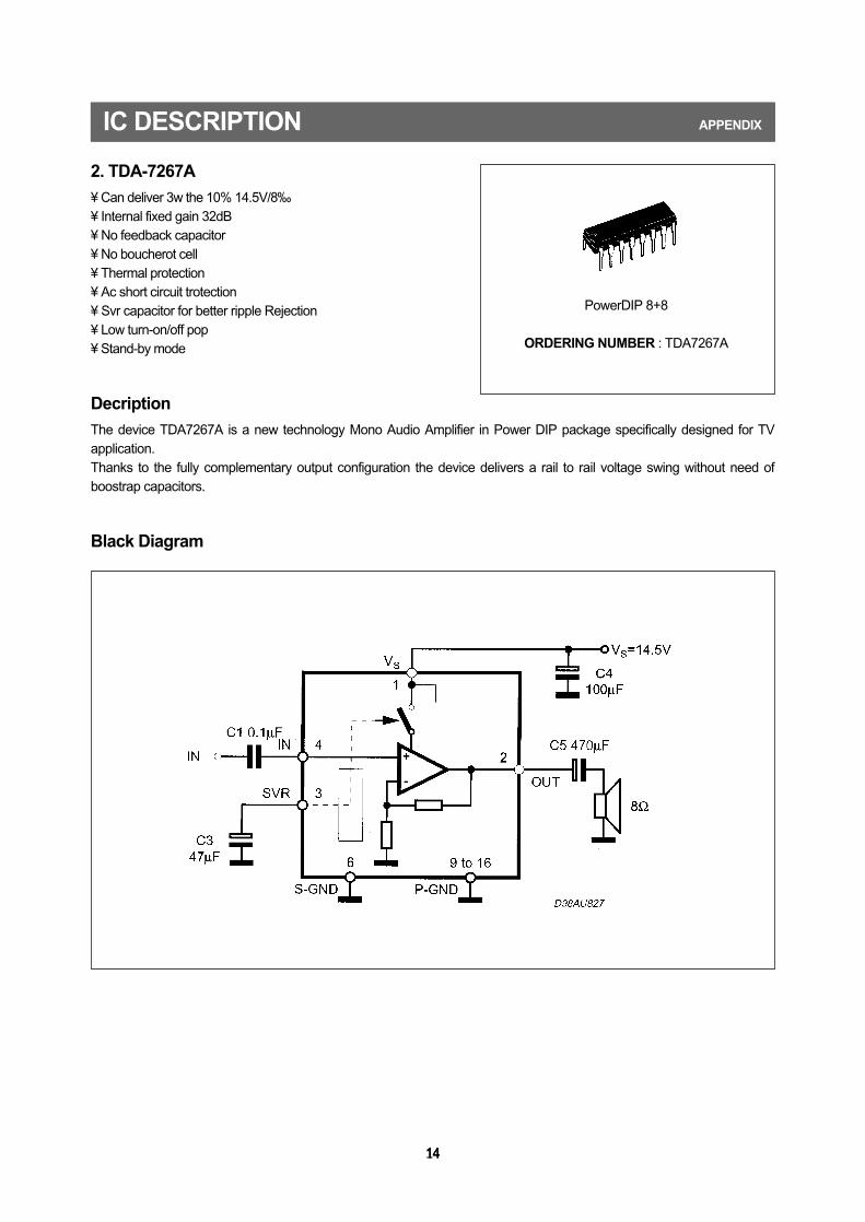
2. TDA-7267A
¥ Can deliver 3w the 10% 14.5V/8‰¥ Internal fixed gain 32dB¥ No feedback capacitor¥ No boucherot cell¥ Thermal protection¥ Ac short circuit trotection¥ Svr capacitor for better ripple Rejection¥ Low turn-on/off pop¥ Stand-by mode
Decription
The device TDA7267A is a new technology Mono Audio Amplifier in Power DIP package specifically designed for TVapplication.Thanks to the fully complementary output configuration the device delivers a rail to rail voltage swing without need ofboostrap capacitors.
Black Diagram
14
IC DESCRIPTION APPENDIX
PowerDIP 8+8
ORDERING NUMBER : TDA7267A
1515
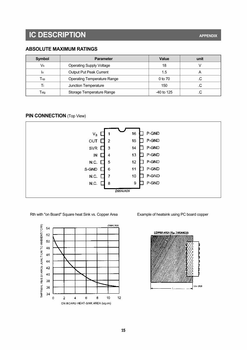
ABSOLUTE MAXIMUM RATINGS
15
IC DESCRIPTION APPENDIX
PIN CONNECTION (Top View)
Rth with "on Board" Square heat Sink vs. Copper Area Example of heatsink using PC board copper
Symbol Parameter Value unit
Vs Operating Supply Voltage 18 V
Io Output Put Peak Current 1.5 A
Top Operating Temperature Range 0 to 70 …C
Ti Junction Temperature 150 …C
Tstg Storage Temperature Range -40 to 125 …C
1616
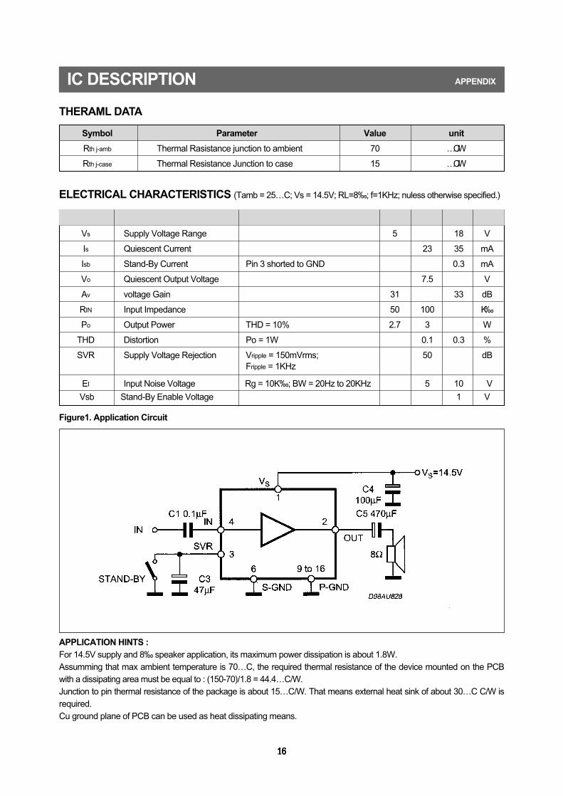
THERAML DATA
Symbol Parameter Test concition Min. Typ. Max. Unit
Vs Supply Voltage Range 5 18 V
Is Quiescent Current 23 35 mA
Isb Stand-By Current Pin 3 shorted to GND 0.3 mA
Vo Quiescent Output Voltage 7.5 V
Av voltage Gain 31 33 dB
RIN Input Impedance 50 100 K‰
Po Output Power THD = 10% 2.7 3 W
THD Distortion Po = 1W 0.1 0.3 %
SVR Supply Voltage Rejection Vripple = 150mVrms; 50 dBFripple = 1KHz
EI Input Noise Voltage Rg = 10K‰; BW = 20Hz to 20KHz 5 10 V
Vsb Stand-By Enable Voltage 1 V
16
IC DESCRIPTION APPENDIX
ELECTRICAL CHARACTERISTICS (Tamb = 25…C; Vs = 14.5V; RL=8‰; f=1KHz; nuless otherwise specified.)
APPLICATION HINTS :For 14.5V supply and 8‰ speaker application, its maximum power dissipation is about 1.8W. Assumming that max ambient temperature is 70…C, the required thermal resistance of the device mounted on the PCBwith a dissipating area must be equal to : (150-70)/1.8 = 44.4…C/W.Junction to pin thermal resistance of the package is about 15…C/W. That means external heat sink of about 30…C C/W isrequired.Cu ground plane of PCB can be used as heat dissipating means.
Figure1. Application Circuit
Symbol Parameter Value unit
Rth j-amb Thermal Rasistance junction to ambient 70 …C/W
Rth j-case Thermal Resistance Junction to case 15 …C/W
1717
3. LA78041
17
IC DESCRIPTION APPENDIX
1818
IC DESCRIPTION APPENDIX
1919
IC DESCRIPTION APPENDIX
2020
IC DESCRIPTION APPENDIX
2121
IC DESCRIPTION APPENDIX
2222
IC DESCRIPTION APPENDIX
23
IC DESCRIPTION APPENDIX
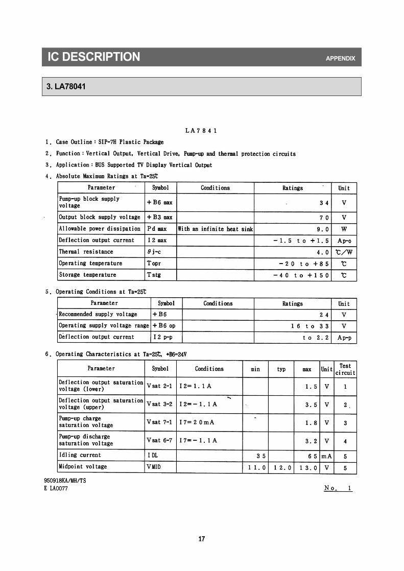
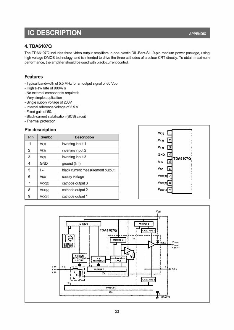
4. TDA6107QThe TDA6107Q includes three video output amplifiers in one plastic DIL-Bent-SIL 9-pin medium power package, usinghigh voltage DMOS technology, and is intended to drive the three cathodes of a colour CRT directly. To obtain maximumperformance, the amplifier should be used with black-current control.
Features- Typical bandwidth of 5.5 MHz for an output signal of 60 Vpp- High slew rate of 900V/ s- No external components requireds- Very simple application- Single supply voltage of 200V- Internal reference voltage of 2.5 V- Fixed gain of 50.- Black-current stabilisation (BCS) circuit- Thermal protection
Pin Symbol Description
1 Vi(1) inverting input 1
2 Vi(2) inverting input 2
3 Vi(3) inverting input 3
4 GND ground (fim)
5 Iom black current measurement output
6 VDD supply voltage
7 VOC(3) cathode output 3
8 VOC(2) cathode output 2
9 VOC(1) cathode output 1
Pin description
24
IC DESCRIPTION APPENDIX
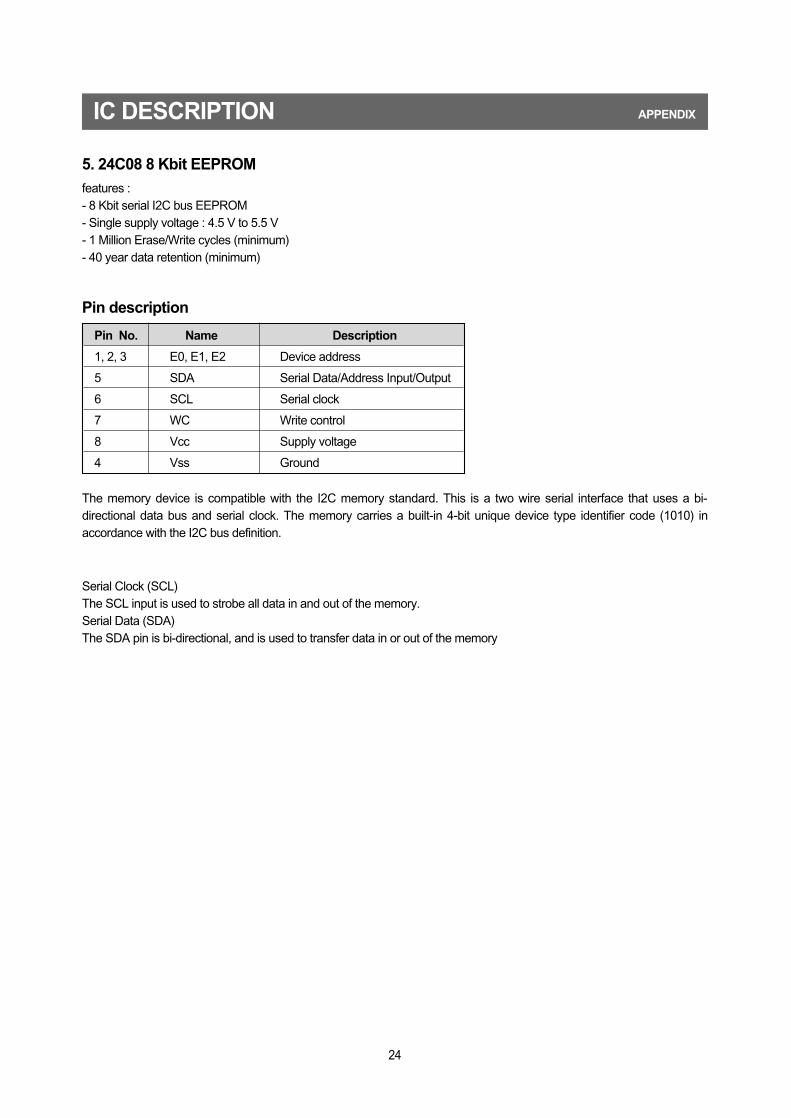
5. 24C08 8 Kbit EEPROM
features :- 8 Kbit serial I2C bus EEPROM- Single supply voltage : 4.5 V to 5.5 V- 1 Million Erase/Write cycles (minimum)- 40 year data retention (minimum)
Pin description
The memory device is compatible with the I2C memory standard. This is a two wire serial interface that uses a bi-directional data bus and serial clock. The memory carries a built-in 4-bit unique device type identifier code (1010) inaccordance with the I2C bus definition.
Serial Clock (SCL)The SCL input is used to strobe all data in and out of the memory.Serial Data (SDA)The SDA pin is bi-directional, and is used to transfer data in or out of the memory
Pin No. Name Description
1, 2, 3 E0, E1, E2 Device address
5 SDA Serial Data/Address Input/Output
6 SCL Serial clock
7 WC Write control
8 Vcc Supply voltage
4 Vss Ground
25
IC DESCRIPTION APPENDIX
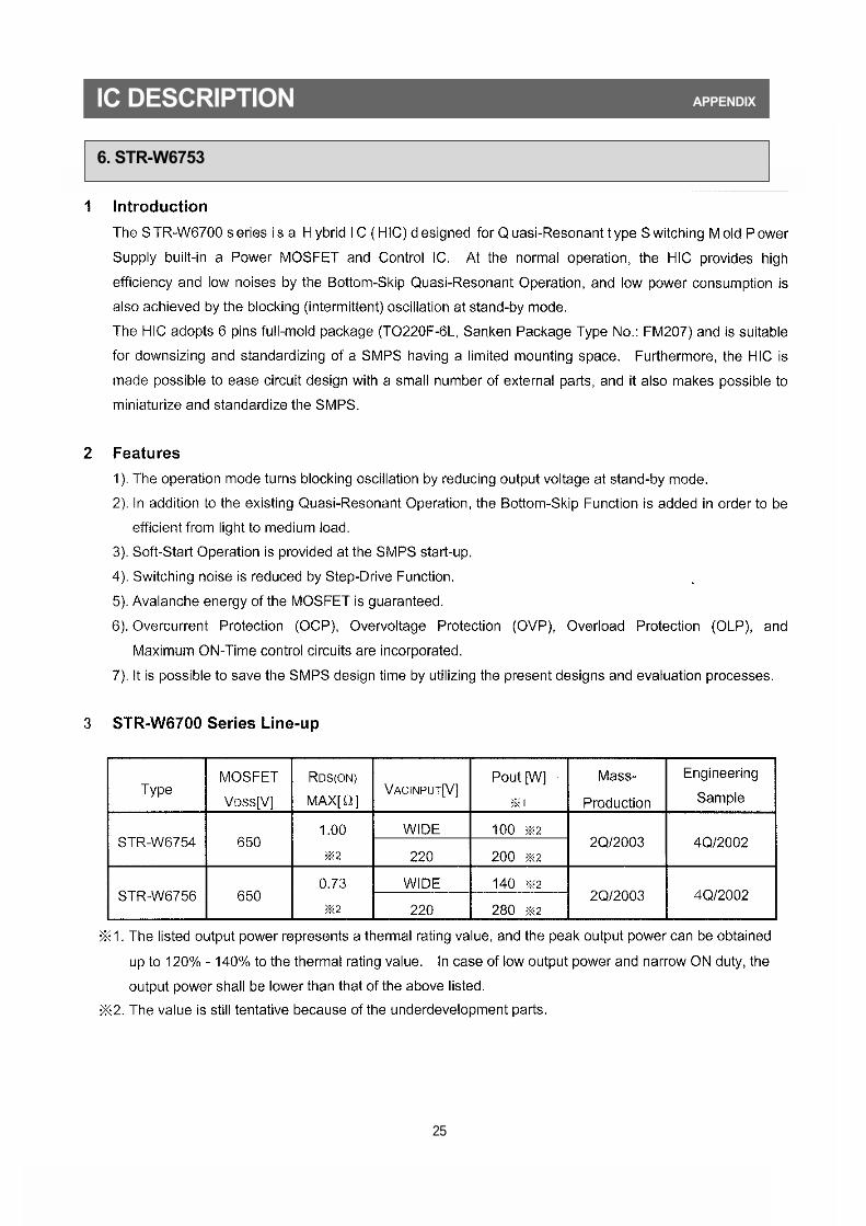
6. STR-W6753
26
IC DESCRIPTION APPENDIX
27
IC DESCRIPTION APPENDIX
28
IC DESCRIPTION APPENDIX
29
IC DESCRIPTION APPENDIX
30
IC DESCRIPTION APPENDIX
31
IC DESCRIPTION APPENDIX
32
IC DESCRIPTION APPENDIX
33
IC DESCRIPTION APPENDIX
34
IC DESCRIPTION APPENDIX
35
IC DESCRIPTION APPENDIX
36
IC DESCRIPTION APPENDIX
37
IC DESCRIPTION APPENDIX
38
IC DESCRIPTION APPENDIX
39
IC DESCRIPTION APPENDIX
40
IC DESCRIPTION APPENDIX
41
IC DESCRIPTION APPENDIX
42
IC DESCRIPTION APPENDIX
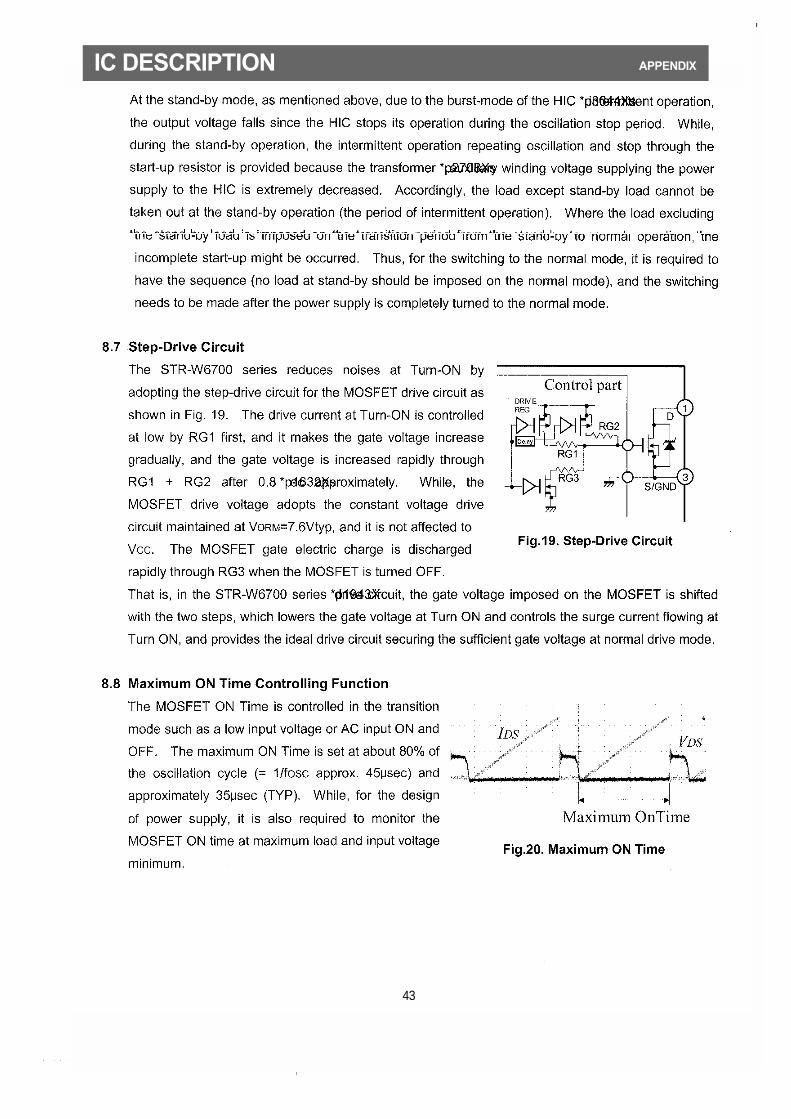
43
IC DESCRIPTION APPENDIX