Embed Size (px)
Citation preview

DAC 2012 Keynote: Designing a 22nm Intel® Architecture Multi-CPU and GPU
Brad Heaney
Copyright © 2012 Intel Corporation

Copyright © 2012 Intel Corporation
3rd generation Intel® Core™ processor (aka Ivy Bridge)
First 22nm, 3-D Tri-Gate microprocessor
Improved Performance & Responsiveness
Power Efficient
Better Graphics & Faster Media Processing
Connected
2

Copyright © 2012 Intel Corporation
3rd Generation Intel® Core™ Processor: 22nm Process
** Cache is shared across all 4 cores and processor graphics
New architecture with shared cache delivering more performance and energy efficiency
Memory Controller I/O
System Agent & Memory
Controller
including DMI, Display and Misc. I/O
Core Core Core Core
Shared L3 Cache
Processor Graphics
3
Copyright © 2012 Intel Corporation
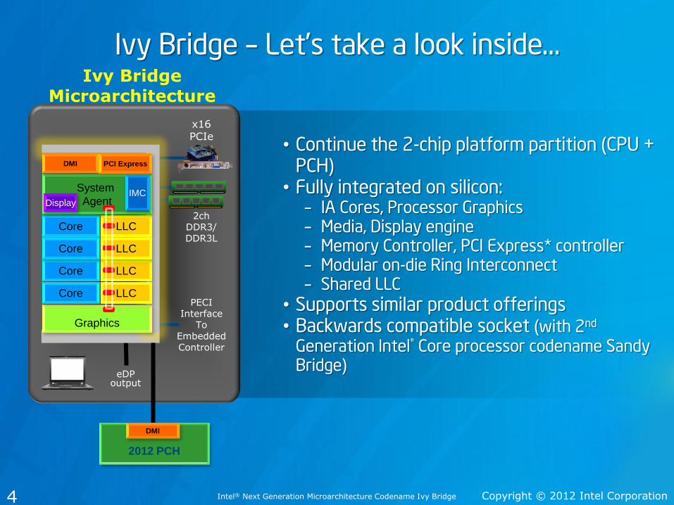
Ivy Bridge – Let’s take a look inside…
4
• Continue the 2-chip platform partition (CPU + PCH)
• Fully integrated on silicon: – IA Cores, Processor Graphics – Media, Display engine – Memory Controller, PCI Express* controller – Modular on-die Ring Interconnect – Shared LLC
• Supports similar product offerings • Backwards compatible socket (with 2nd
Generation Intel® Core processor codename Sandy Bridge)
2ch DDR3/ DDR3L
x16 PCIe
PECI Interface
To Embedded Controller
eDP output
Graphics
Core LLC
Core LLC
Core LLC
Core LLC
System
Agent Display
DMI PCI Express
IMC
2012 PCH
DMI
Ivy Bridge Microarchitecture
Intel® Next Generation Microarchitecture Codename Ivy Bridge

Copyright © 2012 Intel Corporation
Ivy Bridge – Challenges
• Entire chip moves to 22nm
– Higher performance/Lower power
• Graphics/Media
– Higher 3D performance with next generation microarchitecture and Microsoft* DirectX*11
– Up to 2X the graphics performance
• PCI Express 3.0
– Double the speed: 12GB/sec I/O speed
• Security
– Digital Random Number Generator
– Supervisory Mode Execution Protection
• Power Management
– Features for improved battery life
• Memory/Display
– DDR3L support, improved overclocking
– 3 independent displays
5
2ch DDR3/ DDR3L
x16 PCIe
PECI Interface
To Embedded Controller
Graphics
Core LLC
Core LLC
Core LLC
Core LLC
System
Agent Display
DMI PCI Express
IMC
2012 PCH
DMI
Ivy Bridge Microarchitecture
Intel® Next Generation Microarchitecture Codename Ivy Bridge
eDP output
Copyright © 2012 Intel Corporation
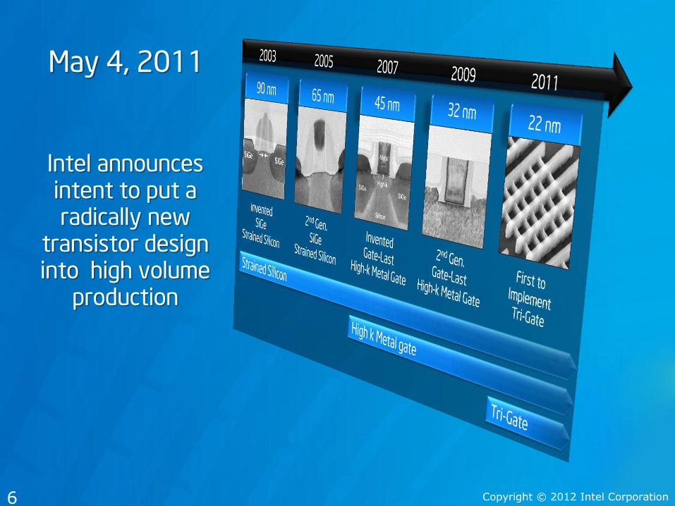
May 4, 2011
Intel announces intent to put a radically new
transistor design into high volume
production
6

Copyright © 2012 Intel Corporation
32nm Sandy Bridge
Sandy Bridge vs. Ivy Bridge
SNB IVB
Die Size 212 mm2 160 mm2
Total Transistors 1.16 B 1.40 B
Core Transistors 79.4 M 80.4 M
GFX Transistors 217 M 416 M
22nm Ivy Bridge
7

Copyright © 2012 Intel Corporation
Composition of CPU’s is Changing
Penryn 45nm
Cache
Westmere 32nm
SandyBridge 32nm
Methods for developing and optimizing process technology need to keep pace with the product content
Cache
IvyBridge 22nm
Cache
Graphics
Graphics
Cach
e
8

Copyright © 2012 Intel Corporation
22nm benefits
Tri-gate device first time in HVM!
Benefits include
Lower operating voltages/power due to exceptional low voltage delay scaling
3 devices with different speed/leakage tradeoffs
Source: M. Bohr, K. Mistry IDF 2011
9

Copyright © 2012 Intel Corporation
Key Capabilities/Methodologies
• Design Re-use:
– Cell-based process migrations
– Modular Graphics Design
• Pre-planned and developed derivatives
– 4 dies from one base design
• Parametric process technology evaluations
10

Copyright © 2012 Intel Corporation
Design Reuse: Cell-based Design Migration
Library Cell
Design Block
Cells Re-design Metals Scaling
Scaled Block
Metal routing
Migration Principals:
Joint process/design development to reduce effort to migrate process from 32nm to 22nm
Speed/Power driven
Preserve design assembly
Cell based
Design Migration approach balances area/power scaling to
achieve lower effort to converge design
11

Copyright © 2012 Intel Corporation
MODULAR GRAPHICS DESIGN
. HALF-SLICE
.
HALF-SLICE
CACHE
SLICE COMMON
MEDIA FIXED
FN INTERF
ACE
EU EU
EU EU
EU EU
EU EU
EU
EU
EU
EU
EU
EU
EU
EU
• Graphics blocks modularly built
• Lower performance graphics derived from high performance graphics design
• Execution units, half slice and the cache banks modularly laid out.
GT2
12

Copyright © 2012 Intel Corporation
Ivy Bridge Dies – Made for quick chops 4+2 2+2, 4+1, 2+1
IP Blocks (Re-use)
IA CORE (template)
SA (System Agent)
Display, GT2, GT1
First number is # of cores, second number is Graphics 13
Copyright © 2012 Intel Corporation
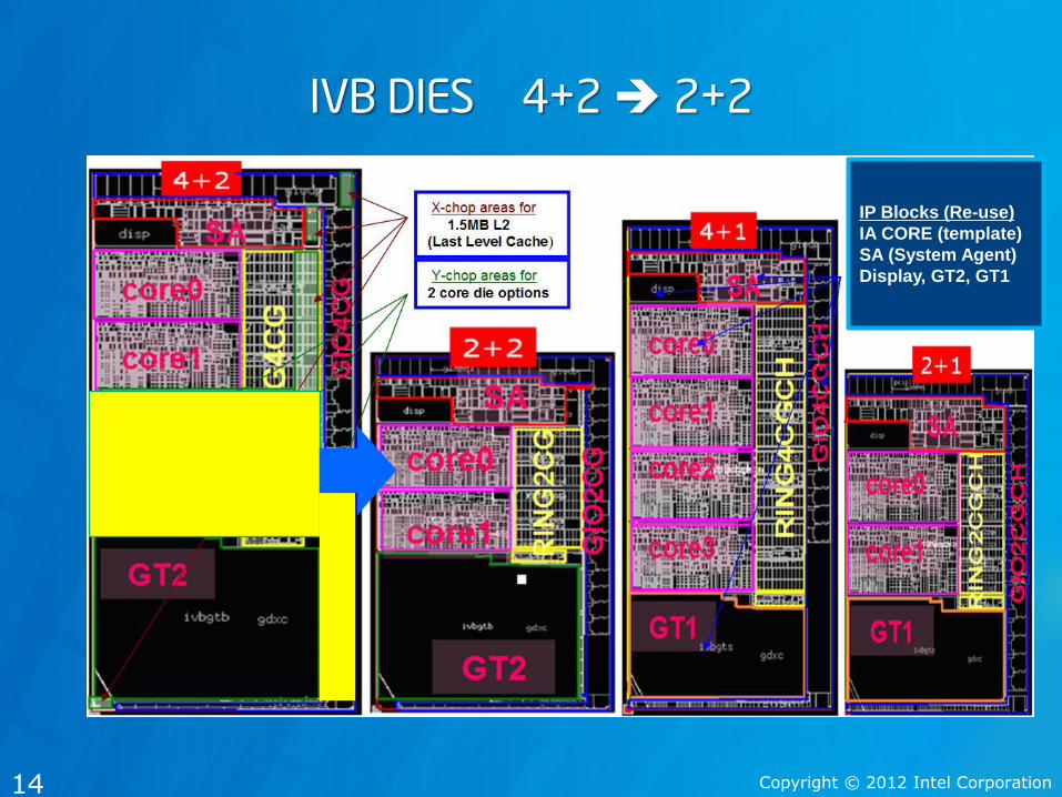
IVB DIES 4+2 2+2
IP Blocks (Re-use)
IA CORE (template)
SA (System Agent)
Display, GT2, GT1
14
Copyright © 2012 Intel Corporation
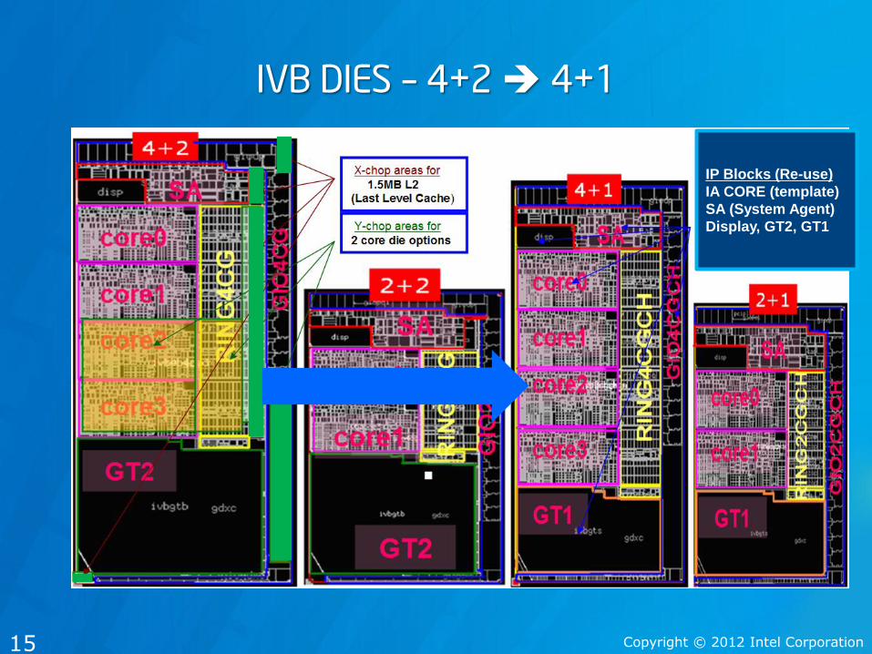
IVB DIES – 4+2 4+1
IP Blocks (Re-use)
IA CORE (template)
SA (System Agent)
Display, GT2, GT1
15

Copyright © 2012 Intel Corporation
IVB DIES – 4+2 2+1
IP Blocks (Re-use)
IA CORE (template)
SA (System Agent)
Display, GT2, GT1
16

Copyright © 2012 Intel Corporation
IVB DIES – Made for quick chops 4+2 2+2, 4+1, 2+1
IP Blocks (Re-use)
IA CORE (template)
SA (System Agent)
Display, GT2, GT1
17

Copyright © 2012 Intel Corporation
Process technology needs for CPU Core vs GFX
• Core is architected to be a narrow & fast:
– Higher frequencies
– Faster and bigger devices
– Taller std-cell library
– Dense power grid & Wider metals
• Gfx is architected be wide & slow:
– Area & Leakage are more critical
– Smaller and lower leakage devices
– Shorter std-cell library,
– Dense layout & Narrower metals
• Future Trend:
– Wider Engines (Frequency less critical)
– Emphasis is on lower power through lower voltage
– Shorter libraries, Denser layout & Narrower Metals
– Higher variation especially for smaller devices
PWR
GND
PWR
GND
Core Std-Cell
GFX Std-Cell
18

Copyright © 2012 Intel Corporation
DFM Requirements & Tool Capabilities
• DFM rules are a key part of the equation for manufacturability:
• Many rules were guidelines but goal is to cover as much area as possible without increasing area
• DFM represents a tradeoff between effort, die-area & manufacturability.
• Future trend:
– DFM rules are getting more critical => No longer guidelines, but design rules & must fix!
– Std-cell library & power grid design etc. need to comprehend them up-front.
– Place & Route tools need to be “DFM aware”
Redundant via
Larger via
Better via enclosure
Min DR Better Best
Contact to Diffusion coverage
19

Copyright © 2012 Intel Corporation
Ivy Bridge Testing and Debug Capabilities
Super high speed, parallel data loading for testing IA cores through DDR for functional/ structural testing
Ability to securely access every part of the chip through IEEE JTAG for control and debug
Sophisticated PCIE debug hooks for logical state machine tracking and debug as well as analog circuit debug to cover for wide process window
Extensive IO debug and testing capabilities including
On die pattern generator, and Jitter margining to test high speed IOs like PCIE Elaborate controls to tune IO ckt parameters
2ch DDR3/ DDR3L
x16 PCIe
PECI Interface
To Embedded Controller
eDP output
Graphics
Core LLC
Core LLC
Core LLC
Core LLC
System
Agent Display
DMI PCI Express
IMC
2012 PCH
DMI
20

Copyright © 2012 Intel Corporation
Ivy Bridge Emulation
Pre-Si Emulation models available 3Q before TI Many Pre-Si bugs found through emulation
Emulation used in many areas:
BIOS boot checkout RTL stress testing GFX SV content checkout GFX driver development Test pattern validation PCIe Gen3
Benefits: Enabled Post Si Validation of Tock features in a Tick schedule
21
Emulation is trending to become a more significant piece of pre-silicon Hardware and software validation

Copyright © 2012 Intel Corporation
22nm Test chip Test chip helped enable process and design convergence
Feedback to process and design teams
Passive elements, Transistor performance and leakage Layout Design rules Robustness and performance of process sensitive circuits
Test chip contents for process sensitive circuits PLLs: LC and self-biased types PCIe Gen3, DDR3 IOs Future Trends: To expand lead process test chip content to include densest standard cell libraries to understand yield impact
Final version of test-chip silicon 1.5 quarters before IvyBridge A-0 silicon
22
Lead process test chip with appropriate analog and
digital content required for TTM
Copyright © 2012 Intel Corporation
Summary • Intel® Next Generation Microarchitecture, Codename Ivy Bridge,
is another big leap in Performance/Power efficiency in both IA core and Graphics/Media
• Next generation Graphics microarchitecture is a Significant Graphics and Media (“tick+”) evolution for Intel® HD Graphics
• Designing a new process technology and product in parallel requires close interaction between design and technology teams
• Collaborative product and process technology development and optimization is key to achieving a winning product
23
It’s Just The Beginning


Copyright © 2012 Intel Corporation
Additional Sources of Information on This Topic:
More web based info on Tri-Gate:
www.intel.com/technology/architecture-silicon/22nm/
25

Copyright © 2012 Intel Corporation
Legal Notices and Disclaimers • INFORMATION IN THIS DOCUMENT IS PROVIDED IN CONNECTION WITH INTEL® PRODUCTS. NO LICENSE, EXPRESS OR
IMPLIED, BY ESTOPPEL OR OTHERWISE, TO ANY INTELLECTUAL PROPERTY RIGHTS IS GRANTED BY THIS DOCUMENT. EXCEPT AS PROVIDED IN INTEL’S TERMS AND CONDITIONS OF SALE FOR SUCH PRODUCTS, INTEL ASSUMES NO LIABILITY WHATSOEVER, AND INTEL DISCLAIMS ANY EXPRESS OR IMPLIED WARRANTY, RELATING TO SALE AND/OR USE OF INTEL® PRODUCTS INCLUDING LIABILITY OR WARRANTIES RELATING TO FITNESS FOR A PARTICULAR PURPOSE, MERCHANTABILITY, OR INFRINGEMENT OF ANY PATENT, COPYRIGHT OR OTHER INTELLECTUAL PROPERTY RIGHT. INTEL PRODUCTS ARE NOT INTENDED FOR USE IN MEDICAL, LIFE SAVING, OR LIFE SUSTAINING APPLICATIONS.
• Intel may make changes to specifications and product descriptions at any time, without notice. • All products, dates, and figures specified are preliminary based on current expectations, and are subject to change
without notice. • Intel, processors, chipsets, and desktop boards may contain design defects or errors known as errata, which may
cause the product to deviate from published specifications. Current characterized errata are available on request. • Any code names featured are used internally within Intel to identify products that are in development and not yet
publicly announced for release. Customers, licensees and other third parties are not authorized by Intel to use code names in advertising, promotion or marketing of any product or services and any such use of Intel's internal code names is at the sole risk of the user.
• Intel product plans in this presentation do not constitute Intel plan of record product roadmaps. Please contact your Intel representative to obtain Intel’s current plan of record product roadmaps.
• Software and workloads used in performance tests may have been optimized for performance only on Intel microprocessors. Performance tests, such as SYSmark and MobileMark, are measured using specific computer systems, components, software, operations and functions. Any change to any of those factors may cause the results to vary. You should consult other information and performance tests to assist you in fully evaluating your contemplated purchases, including the performance of that product when combined with other products. For more information go to http://www.intel.com/performance
• Intel, Intel Inside, the Intel logo, Centrino, Intel Core, Intel Atom, Pentium and UltraBook are trademarks of Intel Corporation in the United States and other countries.
• Material in this presentation is intended as product positioning and not approved end user messaging. • This document contains information on products in the design phase of development. • *Other names and brands may be claimed as the property of others. • Copyright © 2012 Intel Corporation, All Rights Reserved