Embed Size (px)
Citation preview
SEVENTH FRAMEWORK PROGRAMME Theme ICT-2009.1.1
The network of the future
Deliverable D5.2
Work Package 5 – SAMURAI proof-of-concepts
D5.2 Blocks assessment and system evaluation Contract no.: 248268 Project acronym: Samurai Project full title: Spectrum Aggregation and Multi-user MIMO:
Real-World Impact Lead beneficiary: IMC Report preparation date: 31.9.2012 Dissemination level: Public WP5 leader: Florian Kaltenberger WP5 leader organization: Eurecom Revision: 1.0
FP7-INFSO-ICT-248268
SAMURAI
31/01/2012 Public Page 2/62
Table of content 1 Introduction ........................................................................................................................................................... 9 2 MU-MIMO proof-of-concept ............................................................................................................................. 11
2.1 Scope of the MU-MIMO proof of concept demonstrator........................................................................... 11 2.2 Platform description ................................................................................................................................... 11
2.2.1 Software updates .................................................................................................................................... 12 2.2.2 Hardware updates .................................................................................................................................. 12
2.3 Software Developments in SAMURAI ...................................................................................................... 15 2.3.1 Real-time control software ..................................................................................................................... 15 2.3.2 Transmission Mode 5 (MU-MIMO) ...................................................................................................... 16 2.3.3 DCI format 1E ....................................................................................................................................... 17 2.3.4 MU-MIMO Scheduler ........................................................................................................................... 17 2.3.5 Receiver Architecture ............................................................................................................................ 18
2.4 Simulation results ....................................................................................................................................... 19 2.4.1 Link Level .............................................................................................................................................. 19 2.4.2 System Level ......................................................................................................................................... 21
2.5 Real-time performance evaluation ............................................................................................................. 22 2.5.1 Testbench setup ..................................................................................................................................... 22 2.5.2 Results ................................................................................................................................................... 24
2.6 Summary and Key Recommendations ....................................................................................................... 24 3 Carrier aggregation: ACCS PoC ......................................................................................................................... 25
3.1 Scenario and PoC platform definition ........................................................................................................ 25 3.1.1 Demo Scenario ....................................................................................................................................... 25 3.1.2 The platform: Universal Software Radio Peripheral .............................................................................. 25
3.2 ACCS implementation ............................................................................................................................... 27 3.2.1 ACCS PoC Architectural Solution ......................................................................................................... 27 3.2.2 Development and testing approach and methodology ........................................................................... 28 3.2.3 USRP-based PHY Support Implementation Solution ............................................................................ 29 3.2.4 USRP-based OTAC Implementation Solution ...................................................................................... 30 3.2.5 ACCS Software Architecture ................................................................................................................. 31 3.2.6 USRP-based PHY Software Architecture .............................................................................................. 32
3.3 Experimental Analysis ............................................................................................................................... 32 3.3.1 Static environment algorithm analysis ................................................................................................... 34 3.3.2 UE position impact ................................................................................................................................ 35 3.3.3 Dynamic environment algorithm analysis ............................................................................................. 37
3.4 Summary and Key Recommendations ....................................................................................................... 38 4 Carrier aggregation: RF/PHY PoC ..................................................................................................................... 39
4.1 Demo scenario ............................................................................................................................................ 39 4.2 Handset reference board ............................................................................................................................. 39
4.2.1 Introduction............................................................................................................................................ 39 4.2.2 Setup description ................................................................................................................................... 39 4.2.3 Test and results ...................................................................................................................................... 41 4.2.4 Conclusions and lesson learned ............................................................................................................. 44
4.3 Eurecom Express MIMO board ................................................................................................................. 44 4.4 Lessons learned and key recommendations ............................................................................................... 47
5 Test and measurement equipment ....................................................................................................................... 48 5.1 Carrier Aggregated receiver test ................................................................................................................ 48
5.1.1 Introduction............................................................................................................................................ 48 5.1.2 Baseband signal generation.................................................................................................................... 48 5.1.3 Standard compliant baseband signal creator software ........................................................................... 49 5.1.4 RF up-converter ..................................................................................................................................... 51
FP7-INFSO-ICT-248268
SAMURAI
31/01/2012 Public Page 3/62
5.1.5 Conclusion on the receiver test activities ............................................................................................... 51 5.2 Wideband spectrum analysis for CA transmitter test ................................................................................. 51
5.2.1 Motivation.............................................................................................................................................. 51 5.2.2 Instrument architecture .......................................................................................................................... 52 5.2.3 250 MHz spectrum analyzer baseband .................................................................................................. 52 5.2.4 Analysis capabilities .............................................................................................................................. 53 5.2.5 Test results ............................................................................................................................................. 53 5.2.6 Conclusions and lessons learned ............................................................................................................ 55
5.3 Ray-Tracing and deterministic channel emulation ..................................................................................... 55 5.3.1 Deterministic fading .............................................................................................................................. 55 5.3.2 Raygen – the channel data preprocessor ................................................................................................ 55 5.3.3 Conclusions and lessons learned ............................................................................................................ 60
6 Feedback to WP2 ................................................................................................................................................ 61 7 References ........................................................................................................................................................... 62
FP7-INFSO-ICT-248268
SAMURAI
31/01/2012 Public Page 4/62
Table of figures Figure 1-1: Overall SAMURAI demonstrator technologies .......................................................................................... 9 Figure 2-1: Overview of the MU-MIMO PoC ............................................................................................................. 11 Figure 2-2: Express MIMO board ............................................................................................................................... 13 Figure 2-3: RF frontend based on LIME evaluation boards ........................................................................................ 14 Figure 2-4: PA/LNA subsystem .................................................................................................................................. 15 Figure 2-5: Schematics of the real-time control .......................................................................................................... 16 Figure 2-6: MU-MIMO Simulator Process (PHY and MAC) ..................................................................................... 17 Figure 2-7: DCI Format 1E bit fields........................................................................................................................... 17 Figure 2-8: Performance results of IA and IU receiver for MCS9 .............................................................................. 19 Figure 2-9: Performance results of IA and IU receiver for MCS16 ............................................................................ 20 Figure 2-10: Performance results of IA and IU receiver for MCS24 .......................................................................... 20 Figure 2-11: Average System Throughput Comparison .............................................................................................. 22 Figure 2-12: Real-time MU-MIMO testbench ............................................................................................................. 23 Figure 2-13: Schematic of the testbench setup ............................................................................................................ 24 Figure 3-1 – USRP and USRP2 ................................................................................................................................... 26 Figure 3-2: ACCS Testbed Architecture ..................................................................................................................... 27 Figure 3-3: Development process of the ACCS PoC ................................................................................................... 28 Figure 3-4: Software architecture of the eNB node ..................................................................................................... 31 Figure 3-5: Testbed Network Deployment across office rooms. Two positions a) and b) are considered for UE 3 in the experiments ............................................................................................................................................................ 33 Figure 3-6: Experiment1 - Cells’ Capacity CDFs ........................................................................................................ 35 Figure 3-7: Comparison of cells capacity in experiment 1 and 2 ............................................................................... 36 Figure 3-8: Experiment 3; snapshot of channel capacity variations in cells 2 and 3 during the experiment run ......... 37 Figure 4-1: Overview of the setup ............................................................................................................................... 39 Figure 4-2: Picture of the setup ................................................................................................................................... 40 Figure 4-3: Picture of the board ................................................................................................................................... 40 Figure 4-4: constellation of 64QAM-5-6-bandwidth10MHz SISO waveform ........................................................... 42 Figure 4-5: 64QAM-5-6-bandwidth10MHz SISO waveform Wimax details ............................................................ 42 Figure 4-6: Time alignment of the two waveforms ..................................................................................................... 43 Figure 4-7: Schematic of the RF daughter board, highlighting the common clock reference of the two RFICs ......... 43 Figure 4-8: Non real-time testbench for MU-MIMO and CA ..................................................................................... 45 Figure 4-9: Snapshot of the Signal Studio software (running on the PXB) showing the two 5MHz component carriers ......................................................................................................................................................................... 46 Figure 4-10: Snapshot of the OpenAirInterface GUI showing the signals from two CCs ........................................... 46 Figure 5-1: PXB – multiple baseband signal generator, front-view. ........................................................................... 48 Figure 5-2: PXB – multiple baseband signal generator, internal architecture. ............................................................ 49 Figure 5-3: Signal Studio generating standard compliant CA LTE signal. ................................................................. 50 Figure 5-4: SystemVue used to generate customized signals. ..................................................................................... 50 Figure 5-5: MXG RF up-converter. ............................................................................................................................. 51 Figure 5-6: Overall 250 MHz signal analyzer block diagram...................................................................................... 52 Figure 5-7: Development environment. ....................................................................................................................... 53 Figure 5-8: Spectral characteristics for different window choices. .............................................................................. 53 Figure 5-9: Single carrier in 250 MHz frequency span. .............................................................................................. 54 Figure 5-10: Two carriers about 100 MHz apart in 250 MHz frequency span. ........................................................... 54 Figure 5-11: Schematic for 2-tone experimental test setup. ........................................................................................ 55 Figure 5-12: Raygen process flow. .............................................................................................................................. 56 Figure 5-13: Visualization of ray tracing data in an urbanized zone (top view). ......................................................... 57 Figure 5-14: Snapshot DDIR visualization, from top: propagation delay, AoD azimuth and elevation, AoA azimuth and elevation. ............................................................................................................................................................... 58 Figure 5-15: Trajectory definition in the Raygen tool ................................................................................................. 59
FP7-INFSO-ICT-248268
SAMURAI
31/01/2012 Public Page 5/62
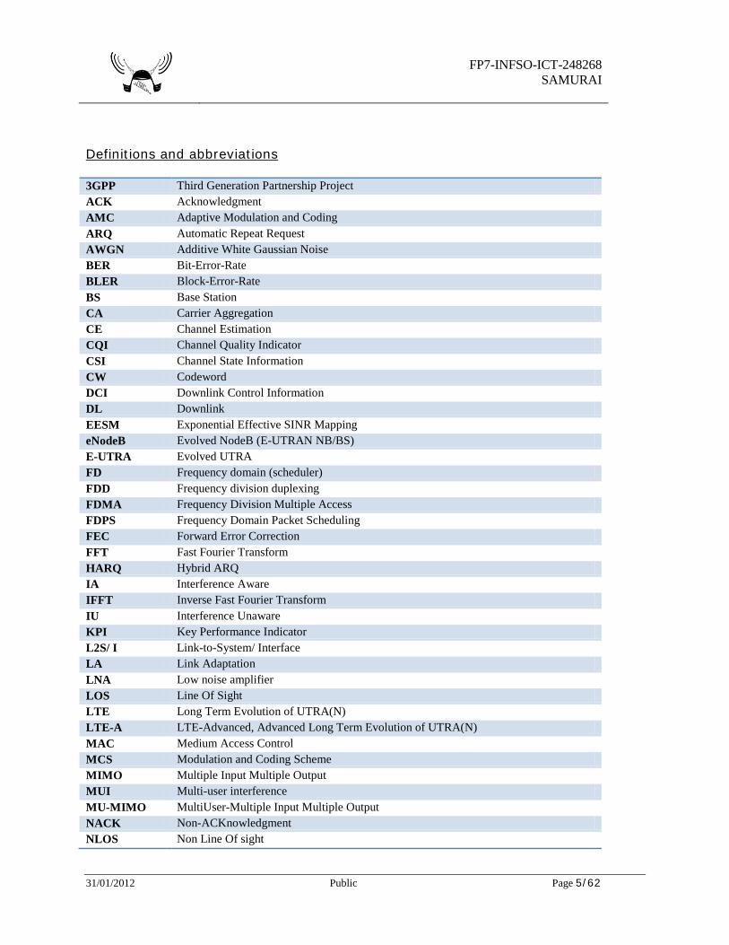
Definitions and abbreviations 3GPP Third Generation Partnership Project ACK Acknowledgment AMC Adaptive Modulation and Coding ARQ Automatic Repeat Request AWGN Additive White Gaussian Noise BER Bit-Error-Rate BLER Block-Error-Rate BS Base Station CA Carrier Aggregation CE Channel Estimation CQI Channel Quality Indicator CSI Channel State Information CW Codeword DCI Downlink Control Information DL Downlink EESM Exponential Effective SINR Mapping eNodeB Evolved NodeB (E-UTRAN NB/BS) E-UTRA Evolved UTRA FD Frequency domain (scheduler) FDD Frequency division duplexing FDMA Frequency Division Multiple Access FDPS Frequency Domain Packet Scheduling FEC Forward Error Correction FFT Fast Fourier Transform HARQ Hybrid ARQ IA Interference Aware IFFT Inverse Fast Fourier Transform IU Interference Unaware KPI Key Performance Indicator L2S/ I Link-to-System/ Interface LA Link Adaptation LNA Low noise amplifier LOS Line Of Sight LTE Long Term Evolution of UTRA(N) LTE-A LTE-Advanced, Advanced Long Term Evolution of UTRA(N) MAC Medium Access Control MCS Modulation and Coding Scheme MIMO Multiple Input Multiple Output MUI Multi-user interference MU-MIMO MultiUser-Multiple Input Multiple Output NACK Non-ACKnowledgment NLOS Non Line Of sight
FP7-INFSO-ICT-248268
SAMURAI
31/01/2012 Public Page 6/62
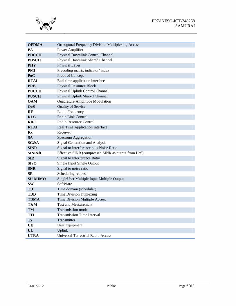
OFDMA Orthogonal Frequency Division Multiplexing Access PA Power Amplifier PDCCH Physical Downlink Control Channel PDSCH Physical Downlink Shared Channel PHY Physical Layer PMI Precoding matrix indicator/ index PoC Proof of Concept RTAI Real time application interface PRB Physical Resource Block PUCCH Physical Uplink Control Channel PUSCH Physical Uplink Shared Channel QAM Quadrature Amplitude Modulation QoS Quality of Service RF Radio Frequency RLC Radio Link Control RRC Radio Resource Control RTAI Real Time Application Interface Rx Receiver SA Spectrum Aggregation SG&A Signal Generation and Analysis SINR Signal to Interference plus Noise Ratio SINReff Effective SINR (compressed SINR as output from L2S) SIR Signal to Interference Ratio SISO Single Input Single Output SNR Signal to noise ratio SR Scheduling request SU-MIMO SingleUser Multiple Input Multiple Output SW SoftWare TD Time domain (scheduler) TDD Time Division Duplexing TDMA Time Division Multiple Access T&M Test and Measurement TM Transmission mode TTI Transmission Time Interval Tx Transmitter UE User Equipment UL Uplink UTRA Universal Terrestrial Radio Access

FP7-INFSO-ICT-248268
SAMURAI
31/01/2012 Public Page 7/62
Contributor list
Name Company Name Company Florian Kaltenberger (editor)
Eurecom Sebastian Wagner Eurecom
Ankit Bhamri Eurecom Irman Latif Eurecom Jonathan Duplicy Agilent Michael Dieudonne Agilent Deepak Tandur Agilent Adnan Al-Adnani Agilent Andrea Cattoni AAU Felice Francesco
Tafuri AAU
Oscar Tonelli AAU Gilberto Berardinelli AAU Biljana Badic IMC Guillaume Vivier Sequans
FP7-INFSO-ICT-248268
SAMURAI
31/01/2012 Public Page 8/62
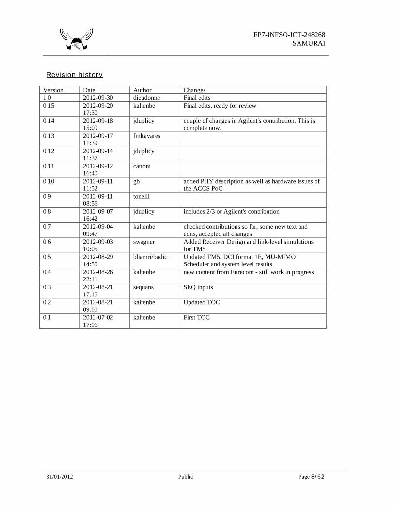
Revision history
Version Date Author Changes 1.0 2012-09-30 dieudonne Final edits 0.15 2012-09-20
17:30 kaltenbe Final edits, ready for review
0.14 2012-09-18 15:09
jduplicy couple of changes in Agilent's contribution. This is complete now.
0.13 2012-09-17 11:39
fmltavares
0.12 2012-09-14 11:37
jduplicy
0.11 2012-09-12 16:40
cattoni
0.10 2012-09-11 11:52
gb added PHY description as well as hardware issues of the ACCS PoC
0.9 2012-09-11 08:56
tonelli
0.8 2012-09-07 16:42
jduplicy includes 2/3 or Agilent's contribution
0.7 2012-09-04 09:47
kaltenbe checked contributions so far, some new text and edits, accepted all changes
0.6 2012-09-03 10:05
swagner Added Receiver Design and link-level simulations for TM5
0.5 2012-08-29 14:50
bhamri/badic Updated TM5, DCI format 1E, MU-MIMO Scheduler and system level results
0.4 2012-08-26 22:11
kaltenbe new content from Eurecom - still work in progress
0.3 2012-08-21 17:15
sequans SEQ inputs
0.2 2012-08-21 09:00
kaltenbe Updated TOC
0.1 2012-07-02 17:06
kaltenbe First TOC
FP7-INFSO-ICT-248268
SAMURAI
31/01/2012 Public Page 9/62
1 Introduction SAMURAI’s development plan has had two main pillars:
• A simulator (developed in WP2), taking care of assessing the impact of the CA and MU-MIMO techniques at system level;
• A proof of concept hardware set of development with the purpose to measure the expected performance of key differentiating algorithms in CA and MU-MIMO field in realistic conditions (developed in WP5).
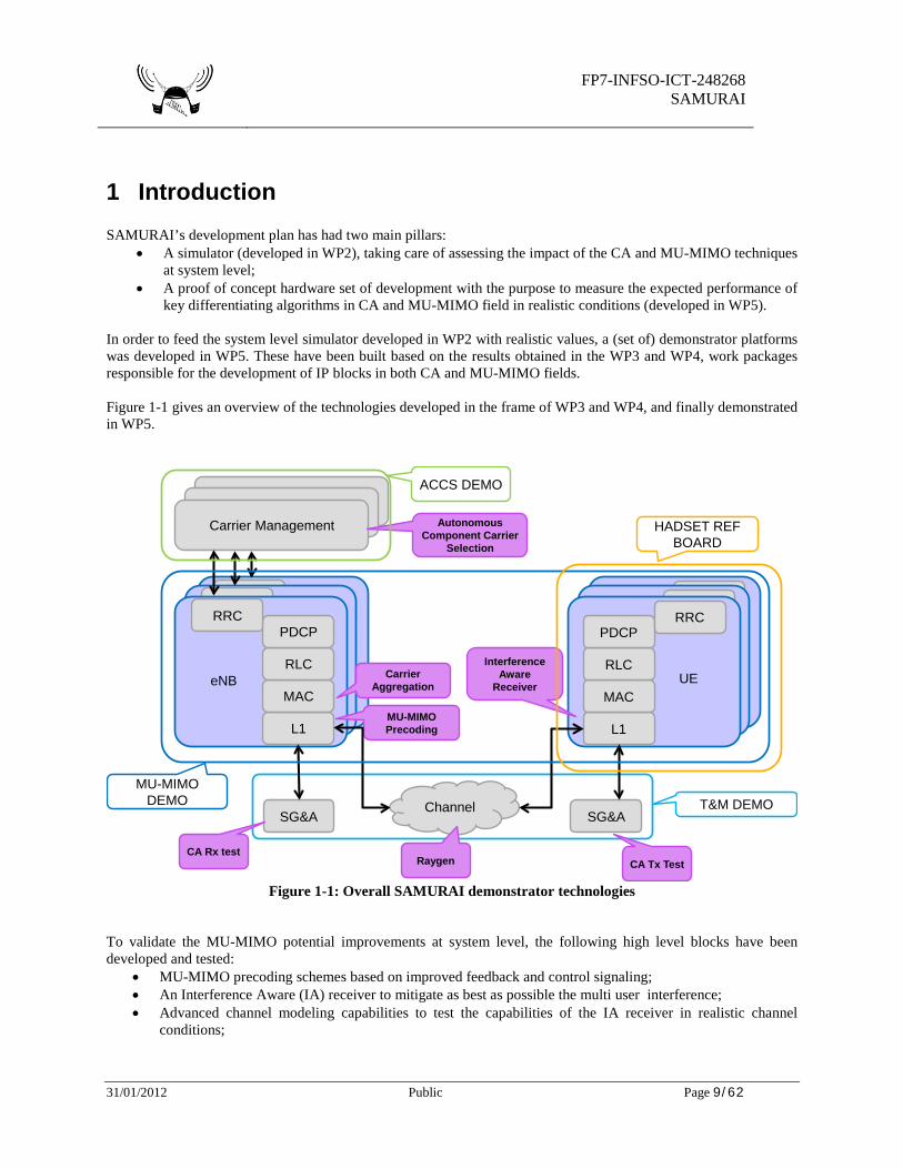
In order to feed the system level simulator developed in WP2 with realistic values, a (set of) demonstrator platforms was developed in WP5. These have been built based on the results obtained in the WP3 and WP4, work packages responsible for the development of IP blocks in both CA and MU-MIMO fields. Figure 1-1 gives an overview of the technologies developed in the frame of WP3 and WP4, and finally demonstrated in WP5.
Figure 1-1: Overall SAMURAI demonstrator technologies
To validate the MU-MIMO potential improvements at system level, the following high level blocks have been developed and tested:
• MU-MIMO precoding schemes based on improved feedback and control signaling; • An Interference Aware (IA) receiver to mitigate as best as possible the multi user interference; • Advanced channel modeling capabilities to test the capabilities of the IA receiver in realistic channel
conditions;
RRMRRM
L1
MAC
RLC
PDCPRRC
UE
L1
MAC
RLC
PDCPRRC
UE
L1
MAC
RLC
PDCPRRC
eNB
L1
MAC
RLC
PDCPRRC
eNB
Carrier Management
ChannelSG&A SG&A
CA Tx Test
L1
MAC
RLC
PDCPRRC
UE
L1
MAC
RLC
PDCPRRC
eNB CarrierAggregation
InterferenceAware
Receiver
MU-MIMO Precoding
Autonomous Component Carrier
Selection
MU-MIMO DEMO
ACCS DEMO
T&M DEMO
HADSET REF BOARD
CA Rx testRaygen
FP7-INFSO-ICT-248268
SAMURAI
31/01/2012 Public Page 10/62
• In addition, developments at other layers (MAC, RRC) have been performed in order to come to a coherent relevant demonstration platform with the ability to perform real life measurements.
The overall WP5 work for MU-MIMO led to the MU-MIMO DEMO and the T&M DEMO. The detailed information on the results for these developments can be found in Sections 2 and 5.3. From a Carrier Aggregation (CA) point of view, the following blocks have been developed:
• The Autonomous Component Carrier Selection (ACCS), a mechanism which at the carrier management level is responsible to select and configure, based on the radio environment and information exchanged between the nodes, the component carriers to be used for the data transmission.
• Two CA RF and PHY proof of concepts studying the impact of CA on RF front end and baseband architecture for CA enabled handsets. One starting from an existing commercial UE system, taking into account the current architectural constrains of e.g. shared Local Oscillator and one starting from a platform having two completely independent RF chains.
• Test and measurement related capabilities in order to assess both the transmission and the analysis of CA signals.
The overall WP5 work for CA led to the ACCS DEMO, HANDSET REF BOARD and T&M DEMO proof of concepts and the results can be found in Section 3, 4, 5.1, and 5.2 respectively This deliverable summarises the integration effort that it has been carried out in WP5. Further, the deliverable presents a performance assessment of the developed PoCs from the level of the building blocks as well as from the system level. Some of the performance results are selected and conditioned to be used in system level studies in WP2.
FP7-INFSO-ICT-248268
SAMURAI
31/01/2012 Public Page 11/62
2 MU-MIMO proof-of-concept
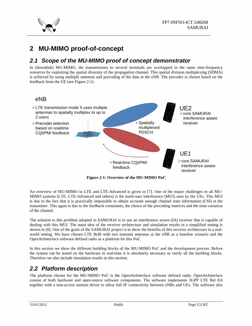
2.1 Scope of the MU-MIMO proof of concept demonstrator In (downlink) MU-MIMO, the transmissions to several terminals are overlapped in the same time-frequency resources by exploiting the spatial diversity of the propagation channel. This spatial division multiplexing (SDMA) is achieved by using multiple antennas and precoding of the data at the eNB. The precoder is chosen based on the feedback from the UE (see Figure 2-1).
Figure 2-1: Overview of the MU-MIMO PoC
An overview of MU-MIMO in LTE and LTE-Advanced is given in [7]. One of the major challenges in all MU-MIMO systems (LTE, LTE-Advanced and others) is the multi-user interference (MUI) seen by the UEs. This MUI is due to the fact that it is practically impossible to obtain accurate enough channel state information (CSI) at the transmitter. This again is due to the feedback constraints, the choice of the precoding matrices and the time-variation of the channel. The solution to this problem adopted in SAMURAI is to use an interference aware (IA) receiver that is capable of dealing with this MUI. The main idea of the receiver architecture and simulation results in a simplified setting is shown in [8]. One of the goals of the SAMURAI project is to show the benefits of this receiver architecture in a real-world setting. We have chosen LTE Rel8 with two transmit antennas at the eNB as a baseline scenario and the OpenAirInterface software defined radio as a platform for this PoC. In this section we show the different building blocks of the MU-MIMO PoC and the development process. Before the system can be tested on the hardware in real-time it is absolutely necessary to verify all the building blocks. Therefore we also include simulation results in this section.
2.2 Platform description The platform chosen for the MU-MIMO PoC is the OpenAirInterface software defined radio. OpenAirInterface consist of both hardware and open-source software components. The software implements 3GPP LTE Rel 8.6 together with a non-access startum driver to allow full IP connectivity between eNBs and UEs. The software also
eNB
UE2
Real - time CQI/PMI feedback
Spatially multiplexed PDSCH
UE1
LTE transmission mode 5 uses multiple antennas to spatially multiplex to up to 2 users Precoder selection
based on real - time CQI/PMI feedback
r uns SAMURAI interference aware receiver
r uns SAMURAI interference aware receiver
FP7-INFSO-ICT-248268
SAMURAI
31/01/2012 Public Page 12/62
features some elements from the LTE-Advanced specifications. An exhaustive overview of the current features of the platform is also given in [11]. The platform has been originally described in D5.1 [5]. In the meantime, several updates to the platform have been made both within the SAMURAI project as well as from other projects. In sections 2.2.1 and 2.2.2 we will only report updates made to the platform in other projects using the same platform. These update are however of importance and re-used by the SAMURAI project. All developments that have been carried out in the frame of the SAMURAI are described in Section 2.3.
2.2.1 Software updates
2.2.1.1 Improvements to the PHY layer • Addition of the PUCCH for ACK/NACK and SR (format 1,1a,1b). The feedback information can still only
be transported on top of a PUSCH transmission.
2.2.1.2 Improvements to the MAC layer • Random access procedures for initial connection establishment • UL/DL HARQ, link adaptation
2.2.1.3 Improvements to the RRC The RRC has been re-implemented based on the open-source ASN1 compiler asn1c (http://lionet.info/asn1c/compiler.html). This allows us to implement the RRC specifications of [3GPP 36.331] with minimum effort. In detail, the following has been implemented
• Messages: RRCConnectionRequest (UE), RRCConnectionSetup (eNB), RRCConnectionSetupComplete (UE), RRCConnectionReconfiguration (eNB), RRCConnectionReconfigurationComplete (UE)
• Procedures : in synch/ out synch indications from PHY, configuration primitives for PHY/MAC (Common, Dedicated configurations)
• Timers : T300,T304,T310 • Counters: N310,N311 • Default DRB configuration, SRB1 + SRB2 activation
2.2.1.4 Improvements to PDCP and RLC • RLC UM/TM/AM modes implemented according to 3GPP 36-321 [4] • PDCP implements black-box interconnection between Linux IP netdevice and RLC user-plane traffic.
2.2.1.5 Emulation platform The OpenAirInterface emulation platform allows to run the full protocol stack of the OpenAirLTE software modem in emulation on one or several PCs. It includes sophisticated channel models, scenario configurations and traffic generators. The PHY layer can also be run in abstraction mode. A more detailed description if the emulation platform is given in [6].
2.2.2 Hardware updates The final MU-MIMO demonstration will make use of the OpenAirInterface ExpressMIMO hardware platform together with a custom built RF frontend based on LIME LMS6002D chips.
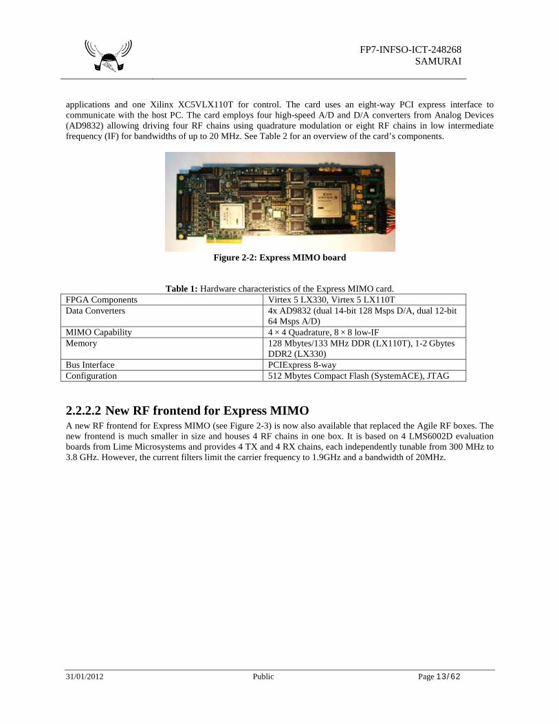
2.2.2.1 Express MIMO Express MIMO (cf Figure 2-2) is a baseband processing board, which provides significantly more processing power and bandwidth than. It comprises two FPGAs: one Xilinx XC5VLX330 for realtime embedded signal processing
FP7-INFSO-ICT-248268
SAMURAI
31/01/2012 Public Page 13/62
applications and one Xilinx XC5VLX110T for control. The card uses an eight-way PCI express interface to communicate with the host PC. The card employs four high-speed A/D and D/A converters from Analog Devices (AD9832) allowing driving four RF chains using quadrature modulation or eight RF chains in low intermediate frequency (IF) for bandwidths of up to 20 MHz. See Table 2 for an overview of the card’s components.
Figure 2-2: Express MIMO board
Table 1: Hardware characteristics of the Express MIMO card. FPGA Components Virtex 5 LX330, Virtex 5 LX110T Data Converters 4x AD9832 (dual 14-bit 128 Msps D/A, dual 12-bit
64 Msps A/D) MIMO Capability 4 × 4 Quadrature, 8 × 8 low-IF Memory 128 Mbytes/133 MHz DDR (LX110T), 1-2 Gbytes
DDR2 (LX330) Bus Interface PCIExpress 8-way Configuration 512 Mbytes Compact Flash (SystemACE), JTAG
2.2.2.2 New RF frontend for Express MIMO A new RF frontend for Express MIMO (see Figure 2-3) is now also available that replaced the Agile RF boxes. The new frontend is much smaller in size and houses 4 RF chains in one box. It is based on 4 LMS6002D evaluation boards from Lime Microsystems and provides 4 TX and 4 RX chains, each independently tunable from 300 MHz to 3.8 GHz. However, the current filters limit the carrier frequency to 1.9GHz and a bandwidth of 20MHz.
FP7-INFSO-ICT-248268
SAMURAI
31/01/2012 Public Page 14/62
J5 connector for the LIME programming
Lime eval board
SMA connectors to the EXPRESS MIMO
(analog BB signals)
N-type connectorsto PA/LNA sub
system(analog RF signals)
Figure 2-3: RF frontend based on LIME evaluation boards
2.2.2.3 PA-LNA subsystem Four power amplifier (PA) and low-noise amplifier (LNA) boxes have also been developed. Each chain of the RF system can be connected to a PA-LNA box (see Figure 2-4) to allow for transmission powers of up to 30dBm. The power amplifiers are currently limited to the 1.9GHz band, where Eurecom has a frequency allocation for experimentation around its premises in Sophia Antipolis. The eNB antennas are typical antennas with dual (cross) polarized ports per sector from Kathrein.
FP7-INFSO-ICT-248268
SAMURAI
31/01/2012 Public Page 15/62
Figure 2-4: PA/LNA subsystem
2.2.2.4 ExpressMIMO firmware and driver The firmware of the Express MIMO card and the corresponding device driver have been updated to support
• 2 TX and 2 RX full duplex at 7.68 MSPS with 16bit resolution • FDD/TDD • Control of ADAC and external Lime RF frontend
2.3 Software Developments in SAMURAI
2.3.1 Real-time control software The real-time control software of OpenAirInterface has been re-implemented in user-space with the help of LXRT; a library that allows to run real-time applications developed using RTAI in user-space. This re-implementation had become necessary, because we encountered unsolvable problems when we were trying to run the LTE software modem in kernel space. Most notably we were not able to guarantee data alignment of signal buffers and thus our optimized code (using SSE instructions) would not run.
MHL19936 transistor
PassbandCavityfilter
Switchingsystem
N-type connector to antenna
ERA 5Power supplyHermetic
box
FP7-INFSO-ICT-248268
SAMURAI
31/01/2012 Public Page 16/62
Figure 2-5: Schematics of the real-time control
An overview of the new real-time control is depicted in Figure 2-5. The main components are the data acquisition (DAQ) and radio frequency (RF) card (in our case Express MIMO), its Linux driver module, the MODEM control software and then the software MODEM itself. The Linux driver provides the interface between the software MODEM and the Express MIMO card. The MODEM control software makes use of the LXRT extension of RTAI to ensure real-time constrains. The synchronization between the card and the MODEM is achieved by a counter on the card that indicates the position of the card within the frame. This counter is polled by the MODEM control; if the counter is bigger than its internal counter it sleeps until the counters match. Otherwise it does the processing on the current slot. If the internal counter is significantly late with respect to the hardware counter, the current slot is dropped and an error is signaled.
2.3.2 Transmission Mode 5 (MU-MIMO) The transmission mode 5 has been implemented on OpenAirInterface for doing MU-MIMO communications. We can configure the base station with two transmit antennas, users with one receiver antenna and schedule maximum two users simultaneously in the same time-frequency resources for downlink. In our implementation, we have made two new developments to carry out system level simulations for MU-MIMO communications. Firstly we have introduced a new DCI format 1E instead of format 1D which exists in LTE Rel. 8. Secondly we have implemented a MU-MIMO scheduler that is based on a pre-processing algorithm which selects orthogonal users for simultaneous downlink transmissions. Section 2.2.3 and 2.2.4 describe DCI format 1E and MU-MIMO Scheduler respectively. As a result of these new developments, the simulator follows the process cycle shown in Figure 2-4.
DAQ +
RF
CardBus PCI
Linux Kernel (2.6)
Real-time
µKernel
Modem control and sync. (synctest)
User Space (LXRT)
Real-time Space
Kernel Space
PHY proc.
thread
MAC/RLC/PDCP/RRC
Decoding Decoding
Linux driver
(oai user ko)
FP7-INFSO-ICT-248268
SAMURAI
31/01/2012 Public Page 17/62
Figure 2-6: MU-MIMO Simulator Process (PHY and MAC)
2.3.3 DCI format 1E In LTE Release 8, DCI format 1D is used for MU-MIMO transmissions in TM5. However, this format has a very limited scope for MU-MIMO because of the amount of information it provides. It supports the feedback mode 3-1 in LTE and informs the user of the PMI only on wideband basis, which is insufficient to extract sizeable gains from MU-MIMO as compared to SU-MIMO. Therefore considering the requirements for MU-MIMO, we proposed and implemented a new DCI format for exploiting the feedback mode 1-2 for MU-MIMO in LTE. With this feedback mode, the user feeds back the PMI for every sub-band rather than once for the entire bandwidth. Figure 2-5 shows the information that is transmitted with our new DCI format 1E. All fields hold the same meaning as in LTE standard.
Figure 2-7: DCI Format 1E bit fields
2.3.4 MU-MIMO Scheduler For performing system level simulations, we implemented a MAC layer scheduler which is based on a pre-processing algorithm that provides the most optimal allocation of resource blocks among the connected users on sub-band basis. The algorithm is as follows:

FP7-INFSO-ICT-248268
SAMURAI
31/01/2012 Public Page 18/62
1. Initially, it starts by selecting a compatible pair of users with orthogonal PMIs for every sub-band which ensures minimization of interference from other user and maximization of desired signal at the receiver.
2. In case of more than one compatible pair, the pair with maximum combined-channel traffic is selected for MU-MIMO transmission in that particular sub-band.
3. However if no compatible pair exists and then a single user with maximum channel traffic is selected for SU-MIMO transmission.
4. The same process is repeated for all the sub-bands and this way a group of users are selected for transmission in their respective modes.
5. But before actually scheduling these selected users, a final step is performed. In this final step, the pre-processor scans through all connected users, compares their channel traffic over entire bandwidth and selects the user with maximum traffic for SU-MIMO. The overall traffic (entire bandwidth)for this SU-MIMO user is compared with the overall traffic of earlier selected users and the better of the two scenarios is finally selected.
2.3.5 Receiver Architecture The receiver computes the log-likelihood ratios (LLRs), i.e., a measure for each bit indicating if the particular bit is more likely to be zero or one. The LLRs are computed for every bit in the codeword and are the input to the channel decoder. The computation of the LLRs is based on the classical maximum a-posteriori probability (MAP) criterion with maxLog approximation. In particular, we implement the so called “interference-aware receiver” (IA) that computes the LLRs under the assumption of a specific constellation for the interfering symbol. Consider a system with transmit antennas and two users, where the UE is endowed with receive antennas. The received signal vector at the desired user reads
where is the channel from the transmitter to the desired user 0, is the concatenated precoding matrix and is the noise vector. The indexes 0 and 1 indicate quantities belonging to either the desired user 0 or the interfering user 1. We further have the precoding vectors , which are assumed to be orthogonal between user 0 and 1, as well as the data symbols and the effective channel . The optimal metric under the MAP criterion with maxLog approximation yields
where denotes the symbol alphabet and . Since the precoding vector of the interfering user is known, we can compute the effective channel of the interfering user. Thus only the interfering symbol constellation is unknown. However, in LTE, it has to be either QPSK, 16QAM or 64QAM. To estimate the interfering symbol constellation is rather involved but it can be assumed that the eNB will try to schedule users with similar constellations, since that will lead to balanced transmit powers on the antennas ports which is highly desirable (more efficient) from the eNB point of view. Hence, the assumption that both the desired symbol constellation and the interfering symbol constellation are identical is justified. The LLR of th bit is given by
The detailed expressions can be found in the Appendix.
FP7-INFSO-ICT-248268
SAMURAI
31/01/2012 Public Page 19/62
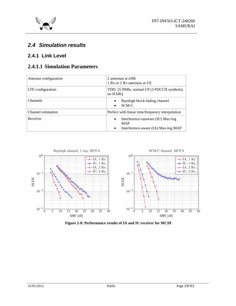
2.4 Simulation results
2.4.1 Link Level
2.4.1.1 Simulation Parameters Antenna configuration 2 antennas at eNB
1 Rx or 2 Rx antennas at UE
LTE configuration TDD, 25 PRBs, normal CP (3 PDCCH symbols), no HARQ
Channels • Rayleigh block-fading channel • SCM-C
Channel estimation Perfect with linear time/frequency interpolation
Receiver • Interference-unaware (IU) Max-log MAP
• Interference-aware (IA) Max-log MAP
Figure 2-8: Performance results of IA and IU receiver for MCS9
FP7-INFSO-ICT-248268
SAMURAI
31/01/2012 Public Page 20/62
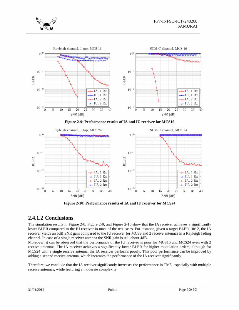
Figure 2-9: Performance results of IA and IU receiver for MCS16
Figure 2-10: Performance results of IA and IU receiver for MCS24
2.4.1.2 Conclusions The simulation results in Figure 2-8, Figure 2-9, and Figure 2-10 show that the IA receiver achieves a significantly lower BLER compared to the IU receiver in most of the test cases. For instance, given a target BLER 10e-2, the IA receiver yields an 5dB SNR gain compared to the IU receiver for MCS9 and 2 receive antennas in a Rayleigh fading channel. In case of a single receiver antenna the SNR gain is still about 4dB. Moreover, it can be observed that the performance of the IU receiver is poor for MCS16 and MCS24 even with 2 receive antennas. The IA receiver achieves a significantly lower BLER for higher modulation orders, although for MCS24 with a single receive antenna, the IA receiver performs poorly. This poor performance can be improved by adding a second receive antenna, which increases the performance of the IA receiver significantly. Therefore, we conclude that the IA receiver significantly increases the performance in TM5, especially with multiple receive antennas, while featuring a moderate complexity.
FP7-INFSO-ICT-248268
SAMURAI
31/01/2012 Public Page 21/62
2.4.2 System Level The simulation parameters for our system level simulations are shown in Figure 2-6.
Table 2: System Level Simulation Parameters
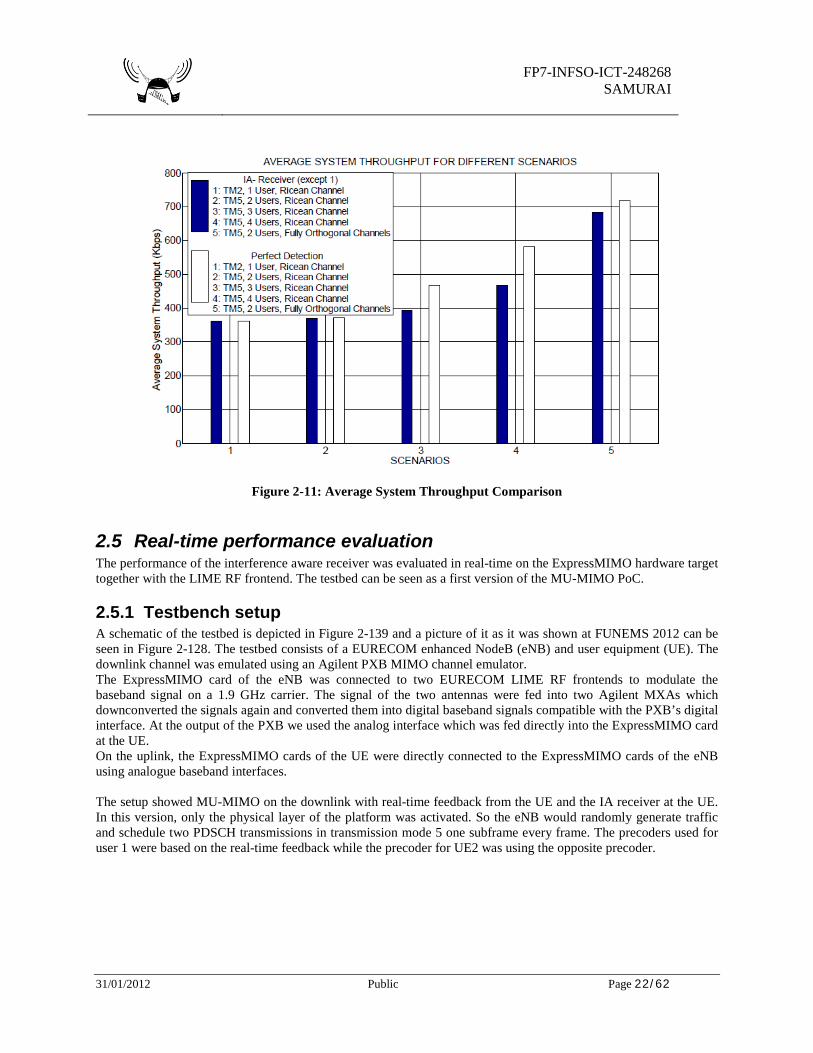
Figure 2-7 gives the performance measurement in terms of average system throughput. Scenario 1 is our base reference scenario in which only 1 user is served in TM2. Scenario 5 is the best case scenario when we have orthogonality for all sub-bands and therefore two users are served for the entire bandwidth in TM5. Apparently the maximum average throughput (scenario 5) is relatively small even at 5MHz bandwidth, since there is only a single subframe has downlink transmission in entire frame for the current configuration of the platform. This scenario is similar to a system having large number of active users since then the probability of full MU-MIMO and the average system throughput will approach Scenario 5. These results also indicate that MU-MIMO gains are not so significant when we have just two active users in the system. However the gains improve gradually with the addition of even few users.
FP7-INFSO-ICT-248268
SAMURAI
31/01/2012 Public Page 22/62
Figure 2-11: Average System Throughput Comparison
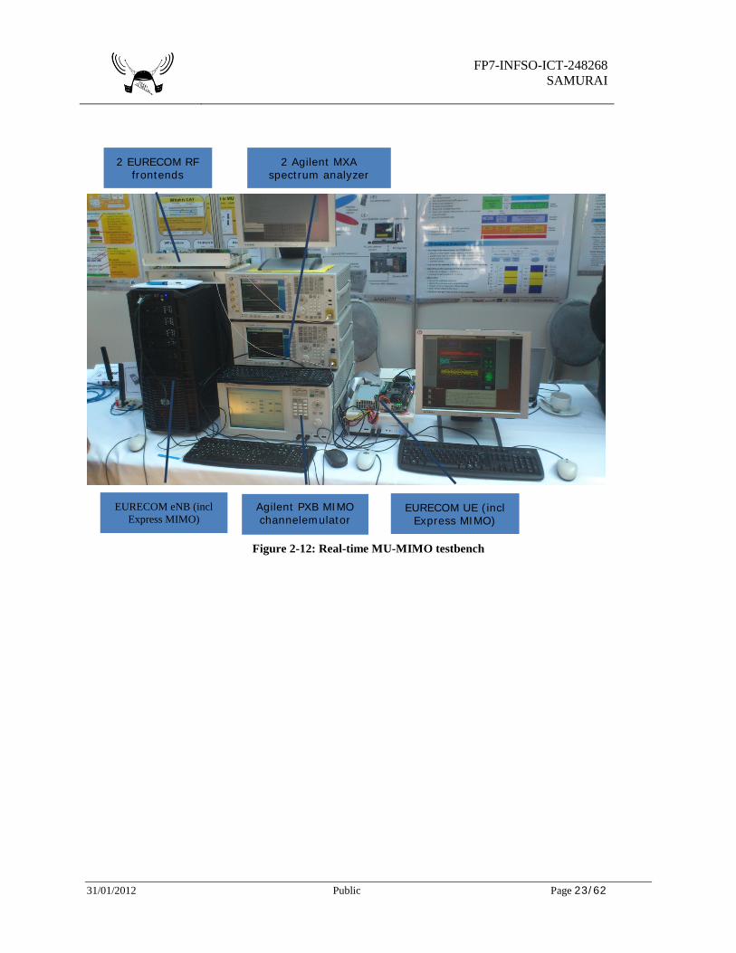
2.5 Real-time performance evaluation The performance of the interference aware receiver was evaluated in real-time on the ExpressMIMO hardware target together with the LIME RF frontend. The testbed can be seen as a first version of the MU-MIMO PoC.
2.5.1 Testbench setup A schematic of the testbed is depicted in Figure 2-139 and a picture of it as it was shown at FUNEMS 2012 can be seen in Figure 2-128. The testbed consists of a EURECOM enhanced NodeB (eNB) and user equipment (UE). The downlink channel was emulated using an Agilent PXB MIMO channel emulator. The ExpressMIMO card of the eNB was connected to two EURECOM LIME RF frontends to modulate the baseband signal on a 1.9 GHz carrier. The signal of the two antennas were fed into two Agilent MXAs which downconverted the signals again and converted them into digital baseband signals compatible with the PXB’s digital interface. At the output of the PXB we used the analog interface which was fed directly into the ExpressMIMO card at the UE. On the uplink, the ExpressMIMO cards of the UE were directly connected to the ExpressMIMO cards of the eNB using analogue baseband interfaces. The setup showed MU-MIMO on the downlink with real-time feedback from the UE and the IA receiver at the UE. In this version, only the physical layer of the platform was activated. So the eNB would randomly generate traffic and schedule two PDSCH transmissions in transmission mode 5 one subframe every frame. The precoders used for user 1 were based on the real-time feedback while the precoder for UE2 was using the opposite precoder.
FP7-INFSO-ICT-248268
SAMURAI
31/01/2012 Public Page 23/62
Figure 2-12: Real-time MU-MIMO testbench
EURECOM eNB (incl Express MIMO)
2 EURECOM RF frontends
2 Agilent MXA spectrum analyzer
EURECOM UE (incl Express MIMO)
Agilent PXB MIMO channelemulator
FP7-INFSO-ICT-248268
SAMURAI
31/01/2012 Public Page 24/62
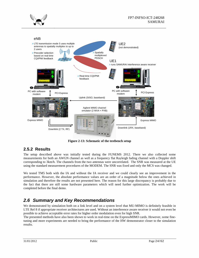
Figure 2-13: Schematic of the testbench setup
2.5.2 Results The setup described above was initially tested during the FUNEMS 2012. There we also collected some measurements for both an AWGN channel as well as a frequency flat Rayleigh fading channel with a Doppler shift corresponding to 3km/h. The channels from the two antennas were uncorrelated. The SNR was measured at the UE using the standard measurement procedures of the MODEM. The SNR was fixed and only the MCS was changed. We tested TM5 both with the IA and without the IA receiver and we could clearly see an improvement in the performance. However, the absolute performance values are an order of a magnitude below the ones achieved in simulation and therefore the results are not presented here. The reason for this large discrepancy is probably due to the fact that there are still some hardware parameters which will need further optimization. The work will be completed before the final demo.
2.6 Summary and Key Recommendations We demonstrated by simulation both on a link level and on a system level that MU-MIMO is definitely feasible in LTE Rel 8 if appropriate receiver architectures are used. Without an interference aware receiver it would not even be possible to achieve acceptable error rates for higher order modulation even for high SNR. The presented methods have also been shown to work in real-time on the ExpressMIMO cards. However, some fine-tuning and more experiments are needed to bring the performance of the HW demonstrator closer to the simulation results.
Express MIMO
PC with software modem
Downlink (2 TX, RF)
PCI Express
eNBUE2(not demonstrated)
Real-time CQI/PMI feedback
Spatially multiplexed PDSCH
PCI ExpressPC with software
modem
Express MIMO
Agilent MIMO channel emulator (2 MXA + PXB)
Downlink (1RX, baseband)
Uplink (SISO, baseband)
UE1
LTE transmission mode 5 uses multiple antennas to spatially multiplex to up to 2 users
Precoder selection based on real-time CQI/PMI feedback
runs SAMURAI interference aware receiver
FP7-INFSO-ICT-248268
SAMURAI
31/01/2012 Public Page 25/62
3 Carrier aggregation: ACCS PoC
3.1 Scenario and PoC platform definition
3.1.1 Demo Scenario This scenario is aimed at reproduce, in practice, the ACCS scenarios explained in both D4.1 and D4.2. This case study is aimed at investigating the component carrier management algorithms in local area deployment scenarios with the main purpose of providing a distributed and autonomous interference management framework. In particular, Local area type scenarios, with indoor eNBs and indoor UEs, have been selected, based on the 3GPP RAN 4 Dense Femtocell Deployment Modelling for "Dual Stripe Model" or "5x5 Grid Model"[9]. The test bed has been also deployed in a way that resembles the deployment models used in simulations. The main challenge of the proposed scenario consists in a severe spectral overcrowding, due to a number of eNBs, each one potentially using two component carriers, greater than the number of available component carriers. The starting assumption of the demonstrator is the presence of multiple eNBs in the same geographical area. Such area is intended to reproduce a typical office or home local area deployment. While in the initial phase of the project and in D4.1, were we have foreseen 4 eNBs, in practice, in the final demonstration we will show up to 6 eNBs, in order to prove the effectiveness of the algorithm in dense and large deployments. Each eNB has one affiliated UE. Only one UE is foreseen since it is out of the scope of the demonstrator to include scheduling capabilities within the developed system. As a matter of fact, this assumption does not affect the validity of the demonstrated concept, since all the system bandwidth, per CC, is anyway used by the UE.
3.1.2 The platform: Universal Software Radio Peripheral The Universal Software Radio Peripherial (USRP) was the platform originally developed to support GNU Radio1. Produced by Ettus Research L.L.C., it provides a software radios using a low-cost external RF hardware and a commodity processor. A complete setup mainly consist of an host PC running software for radio development and a connected USRP platform that provides processing support based on an FPGA and the RF front end. The USRP platform consists in a motherboard providing an FPGA and connection for two daughterboards that serve as RF-front-ends. The basic design philosophy behind the USRP has been to do all of the waveform-specific processing, like modulation and demodulation, on the host CPU. All of the high-speed general purpose operations like digital up and down conversion, decimation and interpolation are done on the FPGA. It could be possible to implement some modulation features in hardware, though, if such features are based on the firmware provided by Ettus, the space for such features in the FPGA is quite restricted.
1 http://gnuradio.org
FP7-INFSO-ICT-248268
SAMURAI
31/01/2012 Public Page 26/62
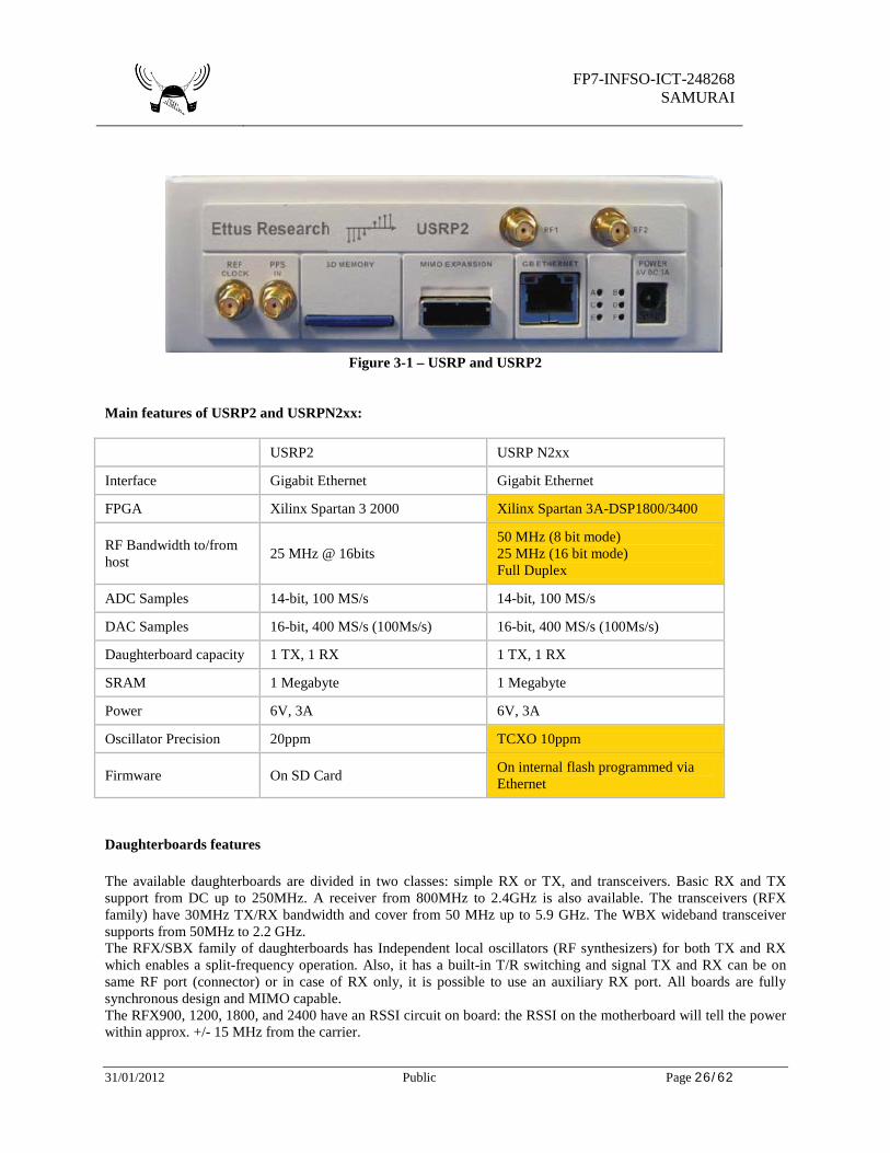
Figure 3-1 – USRP and USRP2
Main features of USRP2 and USRPN2xx: USRP2 USRP N2xx
Interface Gigabit Ethernet Gigabit Ethernet
FPGA Xilinx Spartan 3 2000 Xilinx Spartan 3A-DSP1800/3400
RF Bandwidth to/from host 25 MHz @ 16bits
50 MHz (8 bit mode) 25 MHz (16 bit mode) Full Duplex
ADC Samples 14-bit, 100 MS/s 14-bit, 100 MS/s
DAC Samples 16-bit, 400 MS/s (100Ms/s) 16-bit, 400 MS/s (100Ms/s)
Daughterboard capacity 1 TX, 1 RX 1 TX, 1 RX
SRAM 1 Megabyte 1 Megabyte
Power 6V, 3A 6V, 3A
Oscillator Precision 20ppm TCXO 10ppm
Firmware On SD Card On internal flash programmed via Ethernet
Daughterboards features
The available daughterboards are divided in two classes: simple RX or TX, and transceivers. Basic RX and TX support from DC up to 250MHz. A receiver from 800MHz to 2.4GHz is also available. The transceivers (RFX family) have 30MHz TX/RX bandwidth and cover from 50 MHz up to 5.9 GHz. The WBX wideband transceiver supports from 50MHz to 2.2 GHz. The RFX/SBX family of daughterboards has Independent local oscillators (RF synthesizers) for both TX and RX which enables a split-frequency operation. Also, it has a built-in T/R switching and signal TX and RX can be on same RF port (connector) or in case of RX only, it is possible to use an auxiliary RX port. All boards are fully synchronous design and MIMO capable. The RFX900, 1200, 1800, and 2400 have an RSSI circuit on board: the RSSI on the motherboard will tell the power within approx. +/- 15 MHz from the carrier.
FP7-INFSO-ICT-248268
SAMURAI
31/01/2012 Public Page 27/62
The chosen daughterboard for the SAMURAI project has been the XCVR2450, which is designed to operate in the ISM and UNI bands at 2,4 and 5 GHz.
Universal Hardware Driver (UHD)
The Universal Hardware Driver (UHD) is the official driver for the Ettus Research/USRP products. It provides C++ classes that implement features like metadata addition, clock management and synchronization, abstraction layer for low-level parameters management. The UHD is one of the fundamental blocks for the PHY development in the demonstrator.
3.2 ACCS implementation The ACCS algorithm proof of concept feature a network demonstrator which implements the algorithm features presented in [10]. The demonstrator provides a concrete and tangible picture on how ACCS is able to efficiently manage the spectrum resources in a context of random deployment of the nodes, thus improving the performance of future wireless communications networks. The architecture (logic and software) of the demonstrator components, as well as their implementation details, are presented in the following.
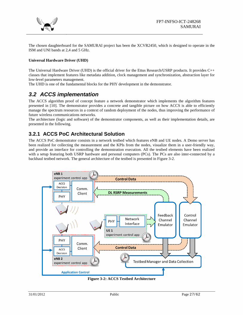
3.2.1 ACCS PoC Architectural Solution The ACCS PoC demonstrator consists in a network testbed which features eNB and UE nodes. A Demo server has been realized for collecting the measurement and the KPIs from the nodes, visualize them in a user-friendly way, and provide an interface for controlling the demonstration execution. All the testbed elements have been realized with a setup featuring both USRP hardware and personal computers (PCs). The PCs are also inter-connected by a backhaul testbed network. The general architecture of the testbed is presented in Figure 3-2.
Figure 3-2: ACCS Testbed Architecture
FP7-INFSO-ICT-248268
SAMURAI
31/01/2012 Public Page 28/62
The ACCS algorithm functionalities execute on the eNB nodes. UEs provide support for downlink (DL) RSRP measurements. Both eNBs and UEs feature a LTE-A-inspired OFDM physical layer. Even though they are designed taking into account some LTE-A aspects, is far from the intention of this demonstrator implement a high-performance PHY. As a matter of fact the transceiver implemented in the nodes includes just the basic and simplified features required for a simple OFDM transmission. The backhaul testbed infrastructure connects all the nodes in the network, providing means for experiment control and testbed data collection. The control channel is emulated by a centralized unit that routes the control data among the nodes. The feedback channel connecting the UEs to the affiliated eNBs is also emulated and enables the reporting of the performed measurements. All the testbed control units, including channel emulators and testbed manager, have been implemented with ASGARD components and can run on any computer connected to the testbed network. The backhaul connections mainly rely on the Ethernet or WiFi interfaces of the PCs. All testbed computers are synchronized to a reference time server with the Network Time Protocol (NTP). This feature provides a common time reference which is crucial for the correct functioning of the ACCS control channel and control of the testbed operations. The NTP protocol provides a synchronization accuracy of few milliseconds. During the demo execution, eNBs and UE continuously report exchanged control data and DL measurements to the Demo Server. The Demo Server application collects the data and updates the information visualized in the graphical user interface (GUI). The user can interact with the GUI and provide input to the demonstrator for modifying the current testbed configuration. Whenever a user input is provided to the Demo Server, a control command message is sent from this to the testbed nodes, triggering their reconfiguration.
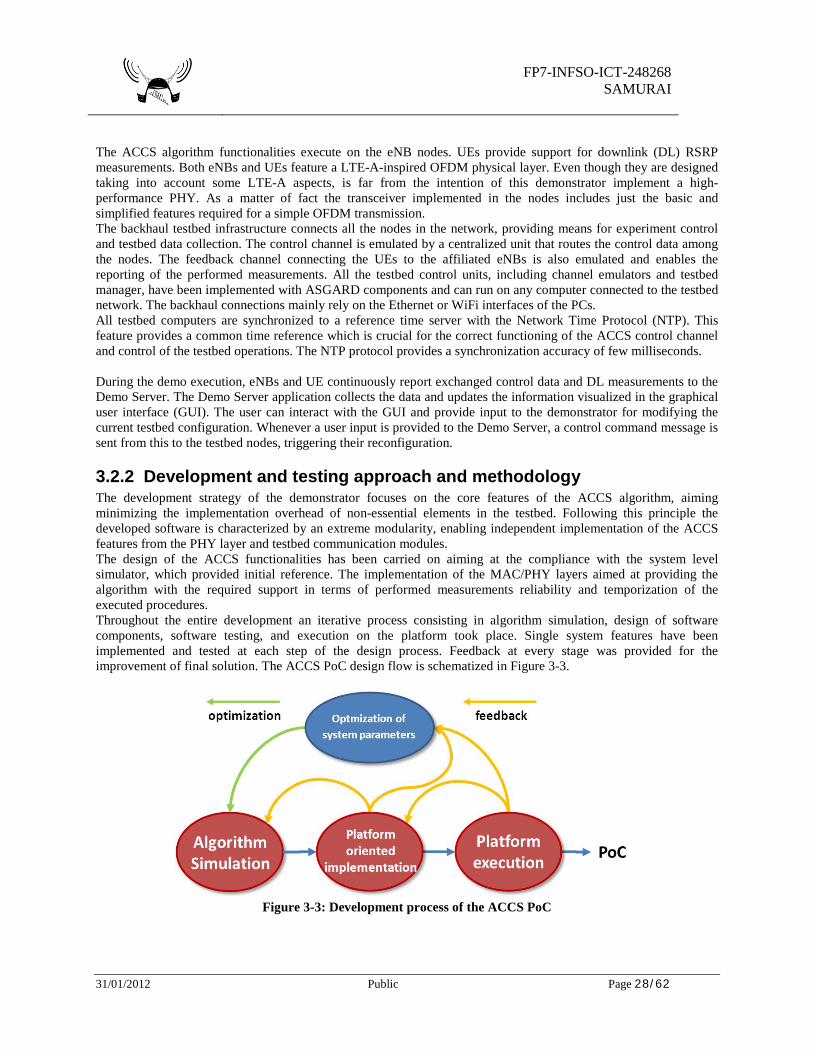
3.2.2 Development and testing approach and methodology The development strategy of the demonstrator focuses on the core features of the ACCS algorithm, aiming minimizing the implementation overhead of non-essential elements in the testbed. Following this principle the developed software is characterized by an extreme modularity, enabling independent implementation of the ACCS features from the PHY layer and testbed communication modules. The design of the ACCS functionalities has been carried on aiming at the compliance with the system level simulator, which provided initial reference. The implementation of the MAC/PHY layers aimed at providing the algorithm with the required support in terms of performed measurements reliability and temporization of the executed procedures. Throughout the entire development an iterative process consisting in algorithm simulation, design of software components, software testing, and execution on the platform took place. Single system features have been implemented and tested at each step of the design process. Feedback at every stage was provided for the improvement of final solution. The ACCS PoC design flow is schematized in Figure 3-3.
Figure 3-3: Development process of the ACCS PoC
FP7-INFSO-ICT-248268
SAMURAI
31/01/2012 Public Page 29/62
Great part of the ACCS PoC process related to the implementation of the system software components. In respect to this specific activity a precise programming technique, namely Test Driven Development (TDD), has been enforced, in order to minimize the code failures and optimizing the re-usability of the developed software features. The TDD foresees the realization of unit tests for the implemented features, prior to the implementation of the features themselves. Such procedures allow to improve the usability of the software components, boosting the efficiency of the code and guaranteeing an almost bug-free implementation.
3.2.3 USRP-based PHY Support Implementation Solution The ACCS algorithm is based on the possibility of performing wideband measurements across the whole spectrum of the reference signals sent by the neighbor eNBs. The ACCS PoC should then provide support for such measurements. The usage of orthogonal frequency pilots univocally associated to each node is a straightforward way for enabling the required sensing capability of the ACCS algorithm. However, the design of the frequency multiplexed pilot patterns has to deal with the non-idealities of the testbed hardware; the limited precision of the local oscillators mounted on the USRP boards leads indeed to frequency offset and phase noise phenomena. The nominal accuracy of the 100 MHz Voltage Controlled Oscillator (VCO) mounted over the USRP2 boards is of 10 ppm, which leads to an expected maximum frequency offset of around +/-50 kHz at a 5 GHz carrier, while the phase noise is estimated to be of around -65 dBc/Hz at 10 kHz offset. The frequency offset can significantly affect the accuracy of the measurements since the received pilots may shift from their nominal frequency position. Moreover, each received pilot may leak its energy to the adjacent frequency bins, thus generating inter-pilots interference. Of course, the problem can be solved by locking both transmit and receive boards to a high precision external reference clock, but this solution would require additional equipment and is not scalable to a large number of nodes. The frequency spacing between different pilot patterns should be then designed according to the experienced power leakage. For example, a practical test has been carried out where an USRP board transmitting a single pilot at 0 dBm in a predefined frequency position is connected via cable to a receiver USRP board, which measures the power in the neighboring frequency bins and average it over a number of 1000 received time vectors. A pilot spacing of 180 kHz turned out to be sufficient for obtaining a power leakage decay below the noise level, thus avoiding inter-pilot interference. It is worth to notice that, in case each node is transmitting a unique pilot tone, the reliability of the RSRP measurements may be affected by the instantaneous fading in that frequency bin. The number of pilots of each transmit node has then to be set with the aim of capturing the frequency selectivity of the channel and average it out. This requirement, together with the frequency spacing one, may pose a severe limit on the testbed scalability for a given available bandwidth. Moreover, the phase noise may cause a further instantaneous random shift of the frequency position of the pilots at the receiver. It is then advisable to integrate the receive power within a limited set of bins centered on the nominal frequency position in order to capture the overall pilot energy. From practical experiments with USRP boards, a power integration over a region of around 60 kHz turned out to achieve the same measurement accuracy which is obtainable with both transmit and receive boards connected to a common external reference clock with 1 ppm precision. While the described physical layer design allows coping with motherboard inaccuracies, the usage of daughterboards affected by unequal transmit/receive power levels can still impact the experimentation outcome. Practical investigations with the Ettus XCVR2450 daughterboards (used with USRP) have shown variations in the transmit/received power up to 10 dB from device to device at the same frequency and with the same reference signal. A statistical validation of the ACCS algorithm over a testbed network requires instead a common reference for aligning transmit power and measurements of each node at each experiment; a calibration procedure needs then to be carried out for both transmit and receive chains. Note that the hardware calibration, which has fundamental importance for the statistical validation of network algorithms, is instead typically disregarded by testbeds focusing on point-to-point applications or opportunistic spectrum usage. The transmit chain can be calibrated by connecting by cable the board to a spectrum analyzer, recording the transmit power level and computing a correction coefficient for aligning the effective power to a reference level. The receiver chain can be instead connected to a high precision signal generator, which outputs a reference signal at a predefined power. Correction coefficients are then computed for aligning the measured power. Furthermore, different boards can also experience different noise floors. For instance, the Analog-to-Digital Converter (ADC) in the USRP N200
FP7-INFSO-ICT-248268
SAMURAI
31/01/2012 Public Page 30/62
board has 3 dB of analog front-end gain with respect to previous versions of the USRP boards, thus reducing the noise level. We suggest to establish a common noise floor for the whole set of boards in the testbed regardless of their effective measured noise. Such common noise floor has reasonably to be set as the highest noise value measured among the testbed boards, despite of a reduction in the dynamic range.
3.2.4 USRP-based OTAC Implementation Solution The testbed features a server that is used as a control channel emulator. The server works as a proxy, routing the messages exchanged among nodes, and as a centralized data collection entity, recording all the exchanged messages. For ACCS demonstrations, the following types of control messages are exchanged:
• eNB RSRP measurements – These messages contain the RSRP measurements for each active interfering cell, in each CC, and are transmitted by the eNBs to the server for data collection and demonstration (GUI) operation only. These messages are used only when the eNB has no active UE associated.
• UE RSRP measurements – These messages contain the RSRP measurements for each active interfering cell, in each CC, as seen from the UE side. The messages are transmitted by the UEs to the server, who records and routes them to the associated eNB.
• BIM + CCRAT – These messages include the ACCS control channel data that is exchanged among eNBs. These messages are also sent by eNBs to the server, who records and routes them to all other eNBs.
All the messages include timestamps and identifiers that allow for the verification of the message exchange process as well for proper operation of the GUI.
FP7-INFSO-ICT-248268
SAMURAI
31/01/2012 Public Page 31/62
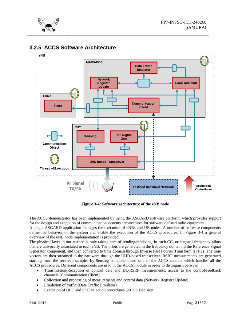
3.2.5 ACCS Software Architecture
Figure 3-4: Software architecture of the eNB node
The ACCS demonstrator has been implemented by using the ASGARD software platform, which provides support for the design and execution of communication systems architectures for software defined radio equipment. A single ASGARD application manages the execution of eNBs and UE nodes. A number of software components define the behavior of the system and enable the execution of the ACCS procedures. In Figure 3-4 a general overview of the eNB node implementation is provided. The physical layer in our testbed is only taking care of sending/receiving, in each CC, orthogonal frequency pilots that are univocally associated to each eNB. The pilots are generated in the frequency domain in the Reference Signal Generator component, and then converted to time domain through Inverse Fast Fourier Transform (IFFT). The time vectors are then streamed to the hardware through the UHD-based transceiver. RSRP measurements are generated starting from the received samples by Sensing component and sent to the ACCS module which handles all the ACCS procedures. Different components are used in the ACCS module in order to distinguish between:
• Transmission/Reception of control data and DL-RSRP measurements, access to the control/feedback channels (Communication Client)
• Collection and processing of measurements and control data (Network Register Update) • Emulation of traffic (Data Traffic Emulator) • Execution of BCC and SCC selection procedures (ACCS Decision)
FP7-INFSO-ICT-248268
SAMURAI
31/01/2012 Public Page 32/62
A timer component is in place to provide the system of basic temporization routines. In order to efficiently meet the different timing requirements of the main system tasks (PHY, MAC/ACCS, Timer) the components are regrouped within separate software modules, each featuring and independent thread of execution. In respect to the eNB, the implementation of the UE is minimal and features only the PHY, Sensing and Communication client components. The purpose of the UE is to periodically provide the affiliated eNB with the DL-RSRP measurements, via the testbed backhaul connection.
3.2.6 USRP-based PHY Software Architecture As mentioned above, the PHY implementation in the ACCS testbed is minimal. The Reference Signal Generator component receives as an input from the ACCS decision component the indexes of the CCs where to transmit, and generates a pilot pattern accordingly. The frequency position of the pilot pattern depends on the ID of the eNB (each pilot pattern is univocally associated to it), so that patterns of multiple eNBs can be multiplexed and then distinguished at the receiver side. The number of pilots for each pattern has to be set according to the available bandwidth per CC and the frequency spacing which is needed to counteract the impact of phase noise and frequency offset due to the hardware inaccuracies. The generated frequency vector is then converted to time domain through IFFT, and then streamed to the UHD transceiver component, which uses the UHD primitives for communicating with the USRP hardware and forward the samples vector to it. When working in receiver mode instead, the UHD transceiver takes care of streaming the downsampled retrieved samples from the hardware. The vector is then forwarded to the Sensing component, which performs the following operations:
• It converts the receive vector to frequency domain through FFT; • It builds a sensing matrix having dimension [Number of CCs x Number of pilot patterns], where the power
measurements for each CC and each eNB are stored. For each pilot, the measurements are integrated in a set of adjacent frequency bins in order to cope with the power leakage due to frequency offset and phase noise.
• It builds a sensing object collecting the sensing matrix and the value of the noise power. The noise power can be measured in the non-occupied frequency bin, or set to a common noise floor value for all the nodes in the testbed.
• The sensing matrix is streamed to the network register update component. Despite of its simplicity, our pilot oriented PHY addresses in an efficient way the necessity of performing wideband sensing which is one of the main assumption of the ACCS algorithm.
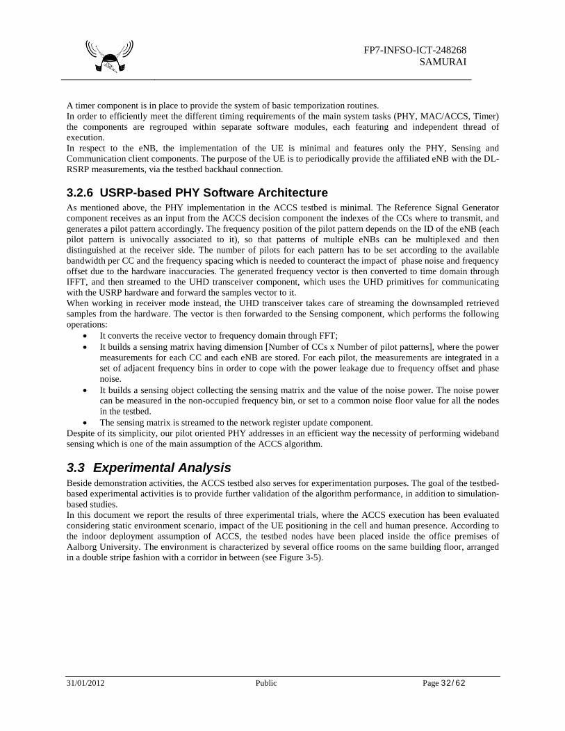
3.3 Experimental Analysis Beside demonstration activities, the ACCS testbed also serves for experimentation purposes. The goal of the testbed-based experimental activities is to provide further validation of the algorithm performance, in addition to simulation-based studies. In this document we report the results of three experimental trials, where the ACCS execution has been evaluated considering static environment scenario, impact of the UE positioning in the cell and human presence. According to the indoor deployment assumption of ACCS, the testbed nodes have been placed inside the office premises of Aalborg University. The environment is characterized by several office rooms on the same building floor, arranged in a double stripe fashion with a corridor in between (see Figure 3-5).
FP7-INFSO-ICT-248268
SAMURAI
31/01/2012 Public Page 33/62
Figure 3-5: Testbed Network Deployment across office rooms. Two positions a) and b) are considered for UE 3 in the experiments
In order to obtain comparable experimental results for the three experiments, an identical spatial deployment of the nodes is considered. The experimental setup features 6 testbed nodes: a configuration with 3 cells is obtained by considering 1 eNB and 1 UE per cell. The cells are also placed in 3 separate rooms with the aim of defining a clear interference scenario. Cell 1 is separated with the corridor, while cells 2 and 3 are placed in contiguous rooms. Two specific configurations for cell 3 have been foreseen: in position a) the eNB 2 is placed very close to the UE 3, thus expecting to generate strong interference; position b) aims at reducing this effect. Despite the limited number of nodes, such deployments provide diversified interference coupling combinations which are challenging for the ACCS performance evaluation. A summary of the performed experiments is provided in Table 3. All experiments share a number of common system configuration parameters that are briefly summarized in Table III.
Table 3: ACCS experiments overview
Experiment 1 2 3
Environment characteristics Static Static Dynamic
Deployment setup a) b) a) CCs configuration 2/3/4 4 4
System Carrier Frequency Variable from 4.91 to 5.81 GHz Variable from 4.91 to 5.81 GHz 5.41 GHz
FP7-INFSO-ICT-248268
SAMURAI
31/01/2012 Public Page 34/62
Table 4: Testbed configuration
Tx power per CC 0 dBm Transceiver I/FFT size 1024 points
Channel configuration 2/3/4 CCs over 12.5 MHz
Total Emulated Bandwidth 12 MHz Antenna configuration SISO ACCS frame 400 ms UE Traffic model Full buffer Target C/I for BCC 10 dB Target C/I for SCC 4 dB
The ACCS algorithm is executed on the testbed in real-time, thus generating time data traces of the eNBs control data and UEs RSRP measurements. These experimental results are processed in order to extract network-wide statistics about downlink SINR experienced in the cells, and the corresponding estimated capacity which is obtained through Shannon mapping. Note that the SINR is first measured on the narrowband pilots, and then scaled to the effective emulated bandwidth of the used CC configuration. Bandwidth scaling is also applied to the Shannon mapping over capacity.
3.3.1 Static environment algorithm analysis The goal of the first experiment is obtaining a general understanding of the algorithm capabilities in a static environment scenario; in particular the impact on the network performance of different number of CCs is analyzed. In order to meet the static environment assumption, the experiment has been executed during night hours. The experiment deployment considers the UE 3 placed in position a) according to Figure 3-5. Iterations with 2, 3 and 4 CCs have been performed. ACCS performance is compared with standard Reuse 1, i.e. each node is transmitting over the whole bandwidth corresponding to the number of configured CC. The amount of experiment runs for each CC configuration is 360, which corresponds to a total of 1080 runs for the entire experiment.
FP7-INFSO-ICT-248268
SAMURAI
31/01/2012 Public Page 35/62
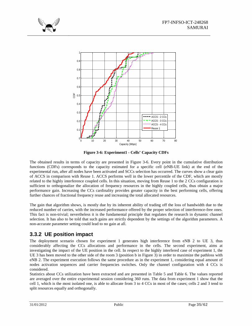
Figure 3-6: Experiment1 - Cells’ Capacity CDFs
The obtained results in terms of capacity are presented in Figure 3-6. Every point in the cumulative distribution functions (CDFs) corresponds to the capacity estimated for a specific cell (eNB-UE link) at the end of the experimental run, after all nodes have been activated and SCCs selection has occurred. The curves show a clear gain of ACCS in comparison with Reuse 1. ACCS performs well in the lower percentile of the CDF, which are mostly related to the highly interference coupled cells. In this situation, moving from Reuse 1 to the 2 CCs configuration is sufficient to orthogonalize the allocation of frequency resources in the highly coupled cells, thus obtain a major performance gain. Increasing the CCs cardinality provides greater capacity in the best performing cells, offering further chances of fractional frequency reuse and increasing the total allocated resources.
The gain that algorithm shows, is mostly due by its inherent ability of trading off the loss of bandwidth due to the reduced number of carries, with the increased performance offered by the proper selection of interference-free ones. This fact is non-trivial; nevertheless it is the fundamental principle that regulates the research in dynamic channel selection. It has also to be told that such gains are strictly dependent by the settings of the algorithm parameters. A non-accurate parameter setting could lead to no gain at all.
3.3.2 UE position impact The deployment scenario chosen for experiment 1 generates high interference from eNB 2 to UE 3, thus considerably affecting the CCs allocations and performance in the cells. The second experiment, aims at investigating the impact of the UE position in the cell. In respect to the highly interfered case of experiment 1, the UE 3 has been moved to the other side of the room 3 (position b in Figure 3) in order to maximize the pathloss with eNB 2. The experiment execution follows the same procedure as in the experiment 1, considering equal amount of nodes activation sequences and carrier frequencies switches. Only the channel configuration with 4 CCs is considered. Statistics about CCs utilization have been extracted and are presented in Table 5 and Table 6. The values reported are averaged over the entire experimental session considering 360 runs. The data from experiment 1 show that the cell 1, which is the most isolated one, is able to allocate from 3 to 4 CCs in most of the cases; cells 2 and 3 tend to split resources equally and orthogonally.
0 10 20 30 40 50 60 70 800
0.1
0.2
0.3
0.4
0.5
0.6
0.7
0.8
0.9
1
Capacity [Mbps]
CD
F
ACCS - 2 CCsACCS - 3 CCsACCS - 4 CCsReuse 1
FP7-INFSO-ICT-248268
SAMURAI
31/01/2012 Public Page 36/62
Table 5: Experiment 1 spectrum usage overview
Cell Spectrum usage (4CCs=100%)
Shared spectrum resources (4CCs=100%) Cell 1 Cell 2 Cell 3
1 84% - 32% 20% 2 48% 32% - 0% 3 48% 20% 0% -
Table 6: Experiment 2 spectrum usage overview
Cell Spectrum usage (4CCs=100%)
Shared spectrum resources (4CCs=100%) Cell 1 Cell 2 Cell 3
1 95% - 45% 53% 2 49% 45% - 5% 3 54% 53% 5% -
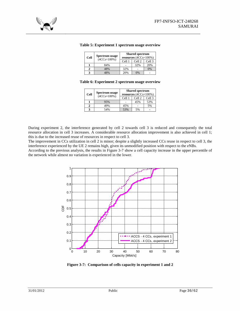
During experiment 2, the interference generated by cell 2 towards cell 3 is reduced and consequently the total resource allocation in cell 3 increases. A considerable resource allocation improvement is also achieved in cell 1; this is due to the increased reuse of resources in respect to cell 3. The improvement in CCs utilization in cell 2 is minor; despite a slightly increased CCs reuse in respect to cell 3, the interference experienced by the UE 2 remains high, given its unmodified position with respect to the eNBs. According to the previous analysis, the results in Figure 3-7 show a cell capacity increase in the upper percentile of the network while almost no variation is experienced in the lower.
Figure 3-7: Comparison of cells capacity in experiment 1 and 2
0 10 20 30 40 50 60 70 800
0.1
0.2
0.3
0.4
0.5
0.6
0.7
0.8
0.9
1
Capacity [Mbit/s]
CD
F
ACCS - 4 CCs, experiment 1ACCS - 4 CCs, experiment 2
FP7-INFSO-ICT-248268
SAMURAI
31/01/2012 Public Page 37/62
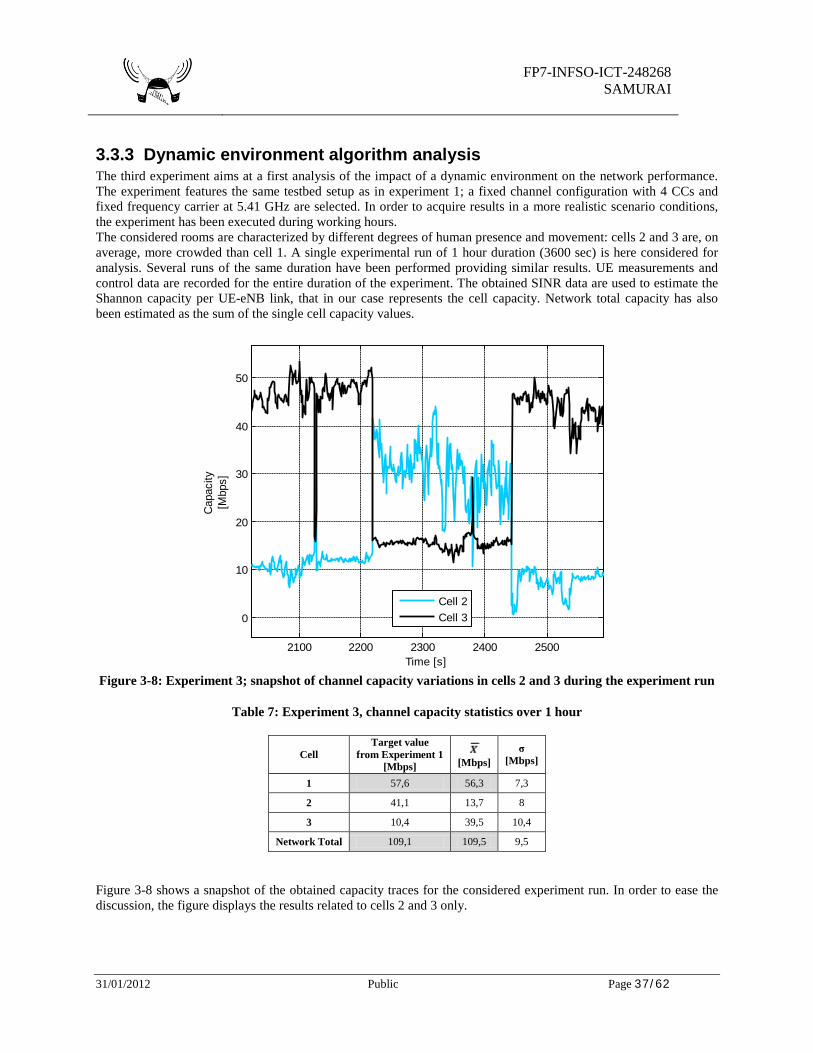
3.3.3 Dynamic environment algorithm analysis The third experiment aims at a first analysis of the impact of a dynamic environment on the network performance. The experiment features the same testbed setup as in experiment 1; a fixed channel configuration with 4 CCs and fixed frequency carrier at 5.41 GHz are selected. In order to acquire results in a more realistic scenario conditions, the experiment has been executed during working hours. The considered rooms are characterized by different degrees of human presence and movement: cells 2 and 3 are, on average, more crowded than cell 1. A single experimental run of 1 hour duration (3600 sec) is here considered for analysis. Several runs of the same duration have been performed providing similar results. UE measurements and control data are recorded for the entire duration of the experiment. The obtained SINR data are used to estimate the Shannon capacity per UE-eNB link, that in our case represents the cell capacity. Network total capacity has also been estimated as the sum of the single cell capacity values.
Figure 3-8: Experiment 3; snapshot of channel capacity variations in cells 2 and 3 during the experiment run
Table 7: Experiment 3, channel capacity statistics over 1 hour
Cell Target value
from Experiment 1 [Mbps]
[Mbps]
σ [Mbps]
1 57,6 56,3 7,3
2 41,1 13,7 8
3 10,4 39,5 10,4
Network Total 109,1 109,5 9,5
Figure 3-8 shows a snapshot of the obtained capacity traces for the considered experiment run. In order to ease the discussion, the figure displays the results related to cells 2 and 3 only.
2100 2200 2300 2400 2500
0
10
20
30
40
50
Cap
acity
[Mbp
s]
Time [s]
Cell 2Cell 3
FP7-INFSO-ICT-248268
SAMURAI
31/01/2012 Public Page 38/62
The impact of a dynamic environment over cells capacity is clearly visible in the time traces: small-scale oscillations of the values are mostly due to SINR variations on the active CCs, larger excursions are instead generated by re-configurations of the allocated CCs. A complete overview of the experiment is provided by the results Table 7. The table reports the time average of cell capacity values ( ), together to the target values obtained by the same experimental scenario (carrier frequency and activation sequences) in static environment conditions (from experiment 1). Standard deviation (σ) is also considered. The obtained results show greater average capacity for cell 1, while cells 2 and 3 are more affected by their mutual interference. Such behaviors are in line with the general indications provided by the previous static environment experiments. The average results across the entire experiment duration are particularly interesting when compared to the specific static environment case. The average capacity of cell 1 is indeed well predicted as well as the total network capacity; the values for cells 2 and 3 are instead considerably different. The different estimation of capacity in respect to the static environment is given by the sensitivity of interference coupled cells, to the environment dynamicity. The ACCS algorithm tends indeed to orthogonalize the allocated CCs between coupled cells. Channel quality variations in time, may lead to the release of resources and therefore full swapping of SCCs between the two cells.
3.4 Summary and Key Recommendations The experimental work in dynamic and static radio environment conditions needs to be jointly pursued in order to obtain a complete insight into the performance of more general and practical carrier aggregation solutions. These types of studies are critical when trying to prove the efficiency of the proposed algorithms, especially when addressing distributed schemes in a network involving several cells. Moreover, the experimentation using a HW/SW test bed is a needed step in order to develop and fine-tune interference management algorithms, while benchmarking with existing simulation studies.
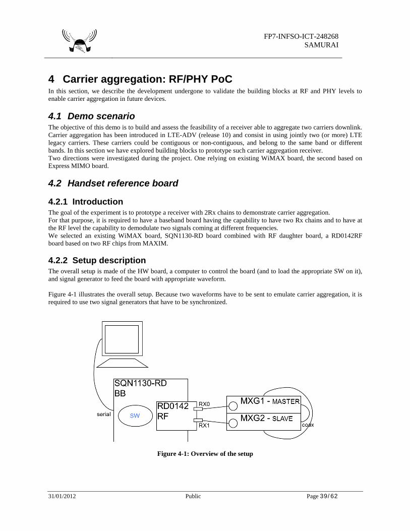
FP7-INFSO-ICT-248268
SAMURAI
31/01/2012 Public Page 39/62
4 Carrier aggregation: RF/PHY PoC In this section, we describe the development undergone to validate the building blocks at RF and PHY levels to enable carrier aggregation in future devices.
4.1 Demo scenario The objective of this demo is to build and assess the feasibility of a receiver able to aggregate two carriers downlink. Carrier aggregation has been introduced in LTE-ADV (release 10) and consist in using jointly two (or more) LTE legacy carriers. These carriers could be contiguous or non-contiguous, and belong to the same band or different bands. In this section we have explored building blocks to prototype such carrier aggregation receiver. Two directions were investigated during the project. One relying on existing WiMAX board, the second based on Express MIMO board.
4.2 Handset reference board
4.2.1 Introduction The goal of the experiment is to prototype a receiver with 2Rx chains to demonstrate carrier aggregation. For that purpose, it is required to have a baseband board having the capability to have two Rx chains and to have at the RF level the capability to demodulate two signals coming at different frequencies. We selected an existing WiMAX board, SQN1130-RD board combined with RF daughter board, a RD0142RF board based on two RF chips from MAXIM.
4.2.2 Setup description The overall setup is made of the HW board, a computer to control the board (and to load the appropriate SW on it), and signal generator to feed the board with appropriate waveform. Figure 4-1 illustrates the overall setup. Because two waveforms have to be sent to emulate carrier aggregation, it is required to use two signal generators that have to be synchronized.
Figure 4-1: Overview of the setup
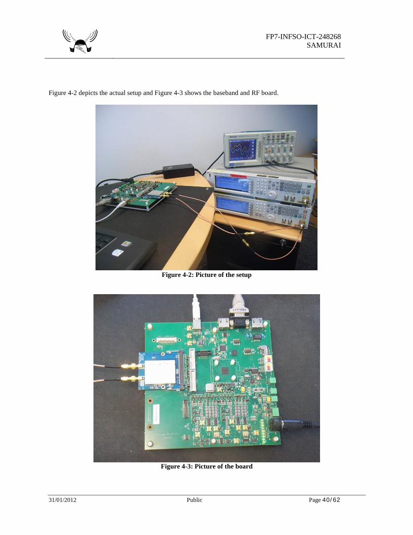
FP7-INFSO-ICT-248268
SAMURAI
31/01/2012 Public Page 40/62
Figure 4-2 depicts the actual setup and Figure 4-3 shows the baseband and RF board.
Figure 4-2: Picture of the setup
Figure 4-3: Picture of the board
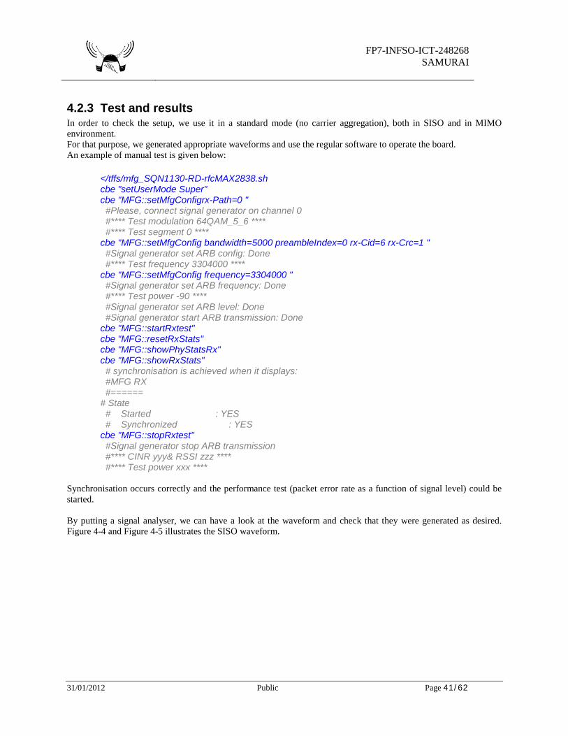
FP7-INFSO-ICT-248268
SAMURAI
31/01/2012 Public Page 41/62
4.2.3 Test and results In order to check the setup, we use it in a standard mode (no carrier aggregation), both in SISO and in MIMO environment. For that purpose, we generated appropriate waveforms and use the regular software to operate the board. An example of manual test is given below:
</tffs/mfg_SQN1130-RD-rfcMAX2838.sh cbe "setUserMode Super" cbe "MFG::setMfgConfigrx-Path=0 " #Please, connect signal generator on channel 0 #**** Test modulation 64QAM_5_6 **** #**** Test segment 0 **** cbe "MFG::setMfgConfig bandwidth=5000 preambleIndex=0 rx-Cid=6 rx-Crc=1 " #Signal generator set ARB config: Done #**** Test frequency 3304000 **** cbe "MFG::setMfgConfig frequency=3304000 " #Signal generator set ARB frequency: Done #**** Test power -90 **** #Signal generator set ARB level: Done #Signal generator start ARB transmission: Done cbe "MFG::startRxtest" cbe "MFG::resetRxStats" cbe "MFG::showPhyStatsRx" cbe "MFG::showRxStats" # synchronisation is achieved when it displays: #MFG RX #====== # State # Started : YES # Synchronized : YES cbe "MFG::stopRxtest" #Signal generator stop ARB transmission #**** CINR yyy& RSSI zzz **** #**** Test power xxx ****
Synchronisation occurs correctly and the performance test (packet error rate as a function of signal level) could be started. By putting a signal analyser, we can have a look at the waveform and check that they were generated as desired. Figure 4-4 and Figure 4-5 illustrates the SISO waveform.
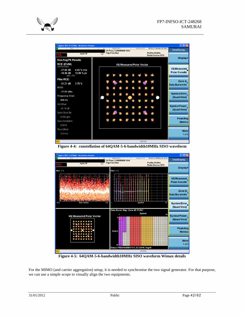
FP7-INFSO-ICT-248268
SAMURAI
31/01/2012 Public Page 42/62
Figure 4-4: constellation of 64QAM-5-6-bandwidth10MHz SISO waveform
Figure 4-5: 64QAM-5-6-bandwidth10MHz SISO waveform Wimax details
For the MIMO (and carrier aggregation) setup, it is needed to synchronise the two signal generator. For that purpose, we can use a simple scope to visually align the two equipments.
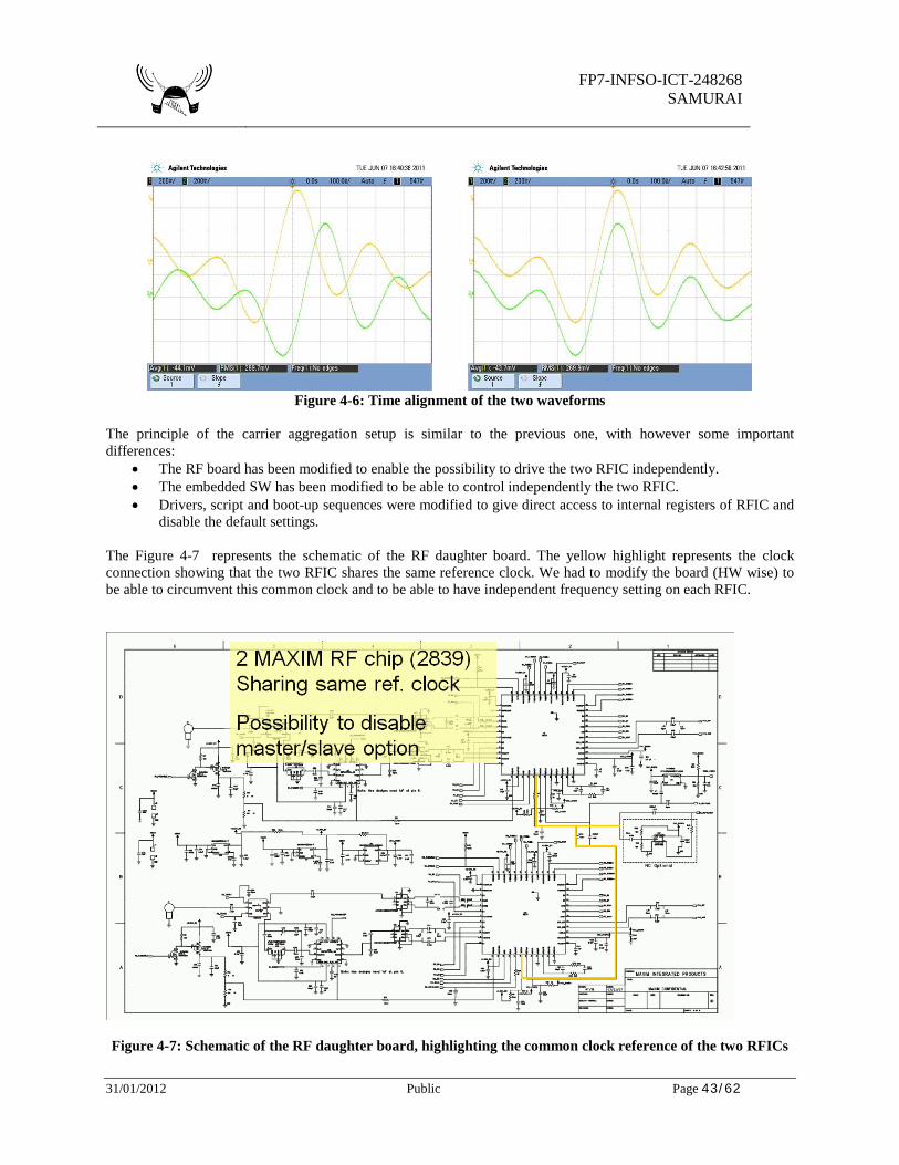
FP7-INFSO-ICT-248268
SAMURAI
31/01/2012 Public Page 43/62
Figure 4-6: Time alignment of the two waveforms
The principle of the carrier aggregation setup is similar to the previous one, with however some important differences:
• The RF board has been modified to enable the possibility to drive the two RFIC independently. • The embedded SW has been modified to be able to control independently the two RFIC. • Drivers, script and boot-up sequences were modified to give direct access to internal registers of RFIC and
disable the default settings. The Figure 4-7 represents the schematic of the RF daughter board. The yellow highlight represents the clock connection showing that the two RFIC shares the same reference clock. We had to modify the board (HW wise) to be able to circumvent this common clock and to be able to have independent frequency setting on each RFIC.
Figure 4-7: Schematic of the RF daughter board, highlighting the common clock reference of the two RFICs
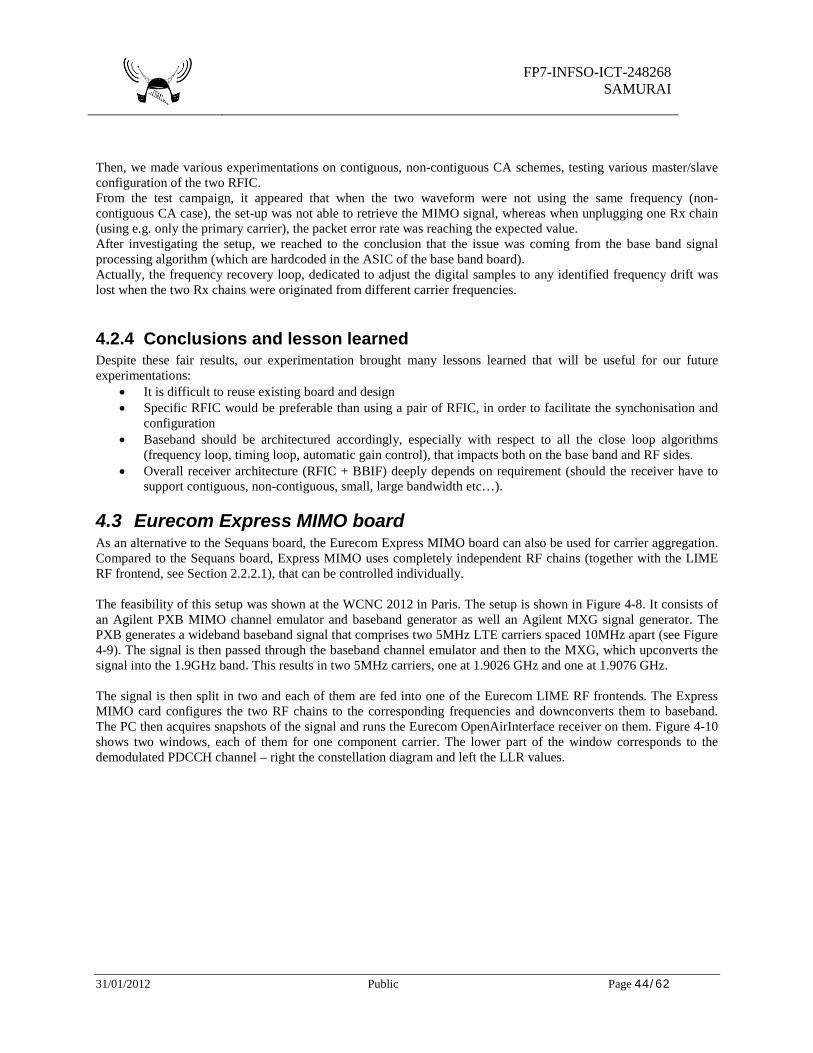
FP7-INFSO-ICT-248268
SAMURAI
31/01/2012 Public Page 44/62
Then, we made various experimentations on contiguous, non-contiguous CA schemes, testing various master/slave configuration of the two RFIC. From the test campaign, it appeared that when the two waveform were not using the same frequency (non-contiguous CA case), the set-up was not able to retrieve the MIMO signal, whereas when unplugging one Rx chain (using e.g. only the primary carrier), the packet error rate was reaching the expected value. After investigating the setup, we reached to the conclusion that the issue was coming from the base band signal processing algorithm (which are hardcoded in the ASIC of the base band board). Actually, the frequency recovery loop, dedicated to adjust the digital samples to any identified frequency drift was lost when the two Rx chains were originated from different carrier frequencies.
4.2.4 Conclusions and lesson learned Despite these fair results, our experimentation brought many lessons learned that will be useful for our future experimentations:
• It is difficult to reuse existing board and design • Specific RFIC would be preferable than using a pair of RFIC, in order to facilitate the synchonisation and
configuration • Baseband should be architectured accordingly, especially with respect to all the close loop algorithms
(frequency loop, timing loop, automatic gain control), that impacts both on the base band and RF sides. • Overall receiver architecture (RFIC + BBIF) deeply depends on requirement (should the receiver have to
support contiguous, non-contiguous, small, large bandwidth etc…).
4.3 Eurecom Express MIMO board As an alternative to the Sequans board, the Eurecom Express MIMO board can also be used for carrier aggregation. Compared to the Sequans board, Express MIMO uses completely independent RF chains (together with the LIME RF frontend, see Section 2.2.2.1), that can be controlled individually. The feasibility of this setup was shown at the WCNC 2012 in Paris. The setup is shown in Figure 4-8. It consists of an Agilent PXB MIMO channel emulator and baseband generator as well an Agilent MXG signal generator. The PXB generates a wideband baseband signal that comprises two 5MHz LTE carriers spaced 10MHz apart (see Figure 4-9). The signal is then passed through the baseband channel emulator and then to the MXG, which upconverts the signal into the 1.9GHz band. This results in two 5MHz carriers, one at 1.9026 GHz and one at 1.9076 GHz. The signal is then split in two and each of them are fed into one of the Eurecom LIME RF frontends. The Express MIMO card configures the two RF chains to the corresponding frequencies and downconverts them to baseband. The PC then acquires snapshots of the signal and runs the Eurecom OpenAirInterface receiver on them. Figure 4-10 shows two windows, each of them for one component carrier. The lower part of the window corresponds to the demodulated PDCCH channel – right the constellation diagram and left the LLR values.
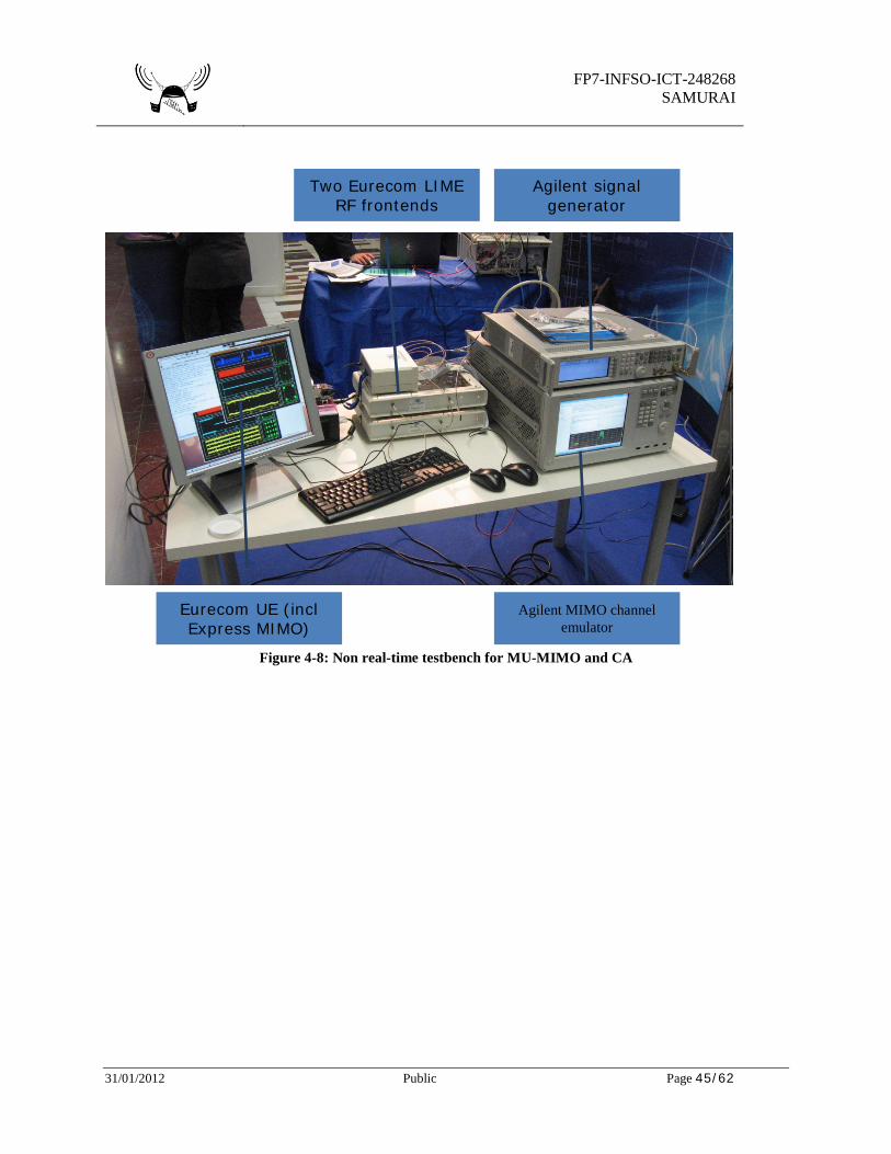
FP7-INFSO-ICT-248268
SAMURAI
31/01/2012 Public Page 45/62
Figure 4-8: Non real-time testbench for MU-MIMO and CA
Agilent MIMO channel emulator
Agilent signal generator
Two Eurecom LIME RF frontends
Eurecom UE (incl Express MIMO)
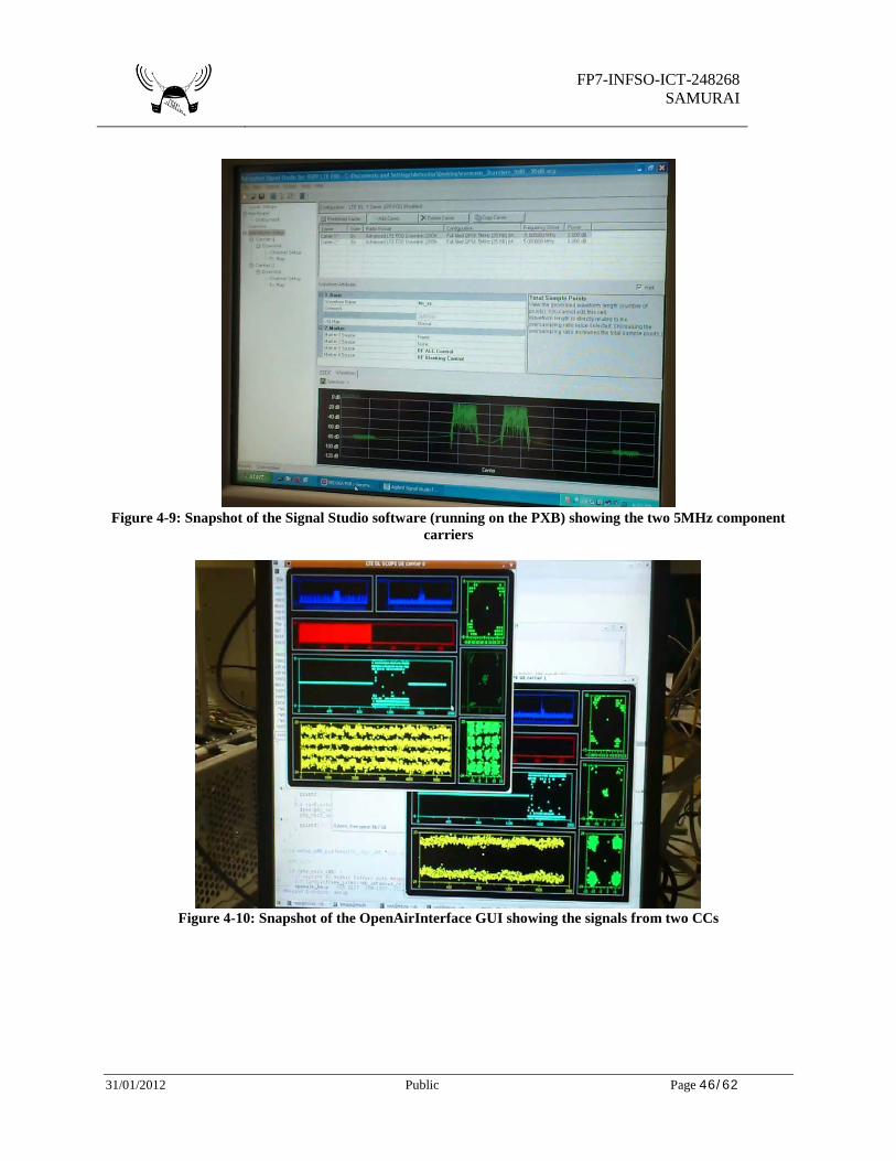
FP7-INFSO-ICT-248268
SAMURAI
31/01/2012 Public Page 46/62
Figure 4-9: Snapshot of the Signal Studio software (running on the PXB) showing the two 5MHz component
carriers
Figure 4-10: Snapshot of the OpenAirInterface GUI showing the signals from two CCs
FP7-INFSO-ICT-248268
SAMURAI
31/01/2012 Public Page 47/62
4.4 Lessons learned and key recommendations From the developments undertaken and the experiments carried out it can be safely said that carrier aggregation is not a trivial task and should be taken care of early in the design stage of a product. As we have seen from the experiments with an existing evaluation board for single carrier communication, it is not feasible to re-use existing hardware. Alternatively, as we have seen from the experiments carried out with the Express MIMO board, a design with independent RF chains is feasible. However this is a rather expensive solution and therefore may not feasible in handheld products. Yet another alternative option is to use specific RF designed to support CA (single RFIC, with more ports to support CA). This is technically feasible to design such an RFIC however, would become quite expensive if it has to support all bands and band combinations. Last but not least, if the aggregated carriers are contiguous or not far apart, wideband sampling is also an option. A key recommendation for the design of carrier aggregation solution is that the RF should not be done independently of the base band, especially with respect to all close loop schemes (AGC, frequency recovery, time recovery, and possibly beamforming, envelop tracking etc.)
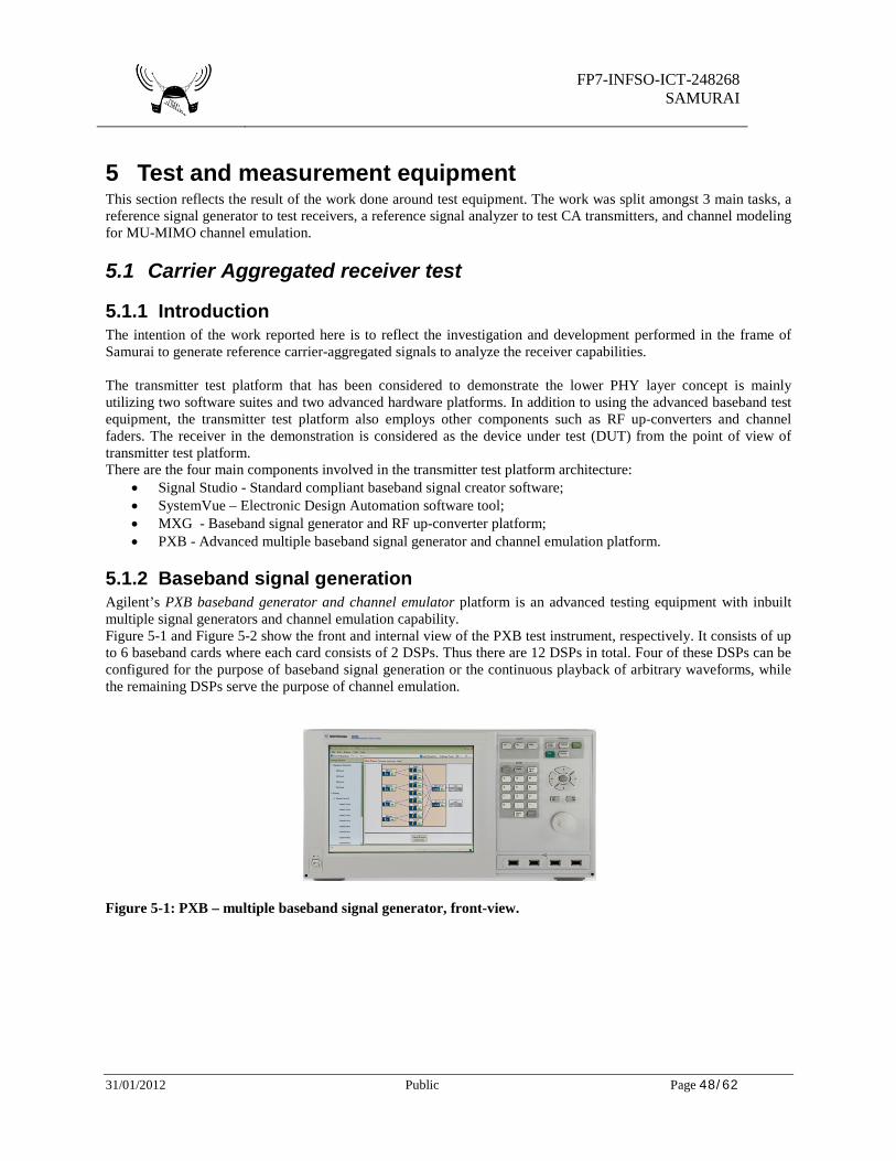
FP7-INFSO-ICT-248268
SAMURAI
31/01/2012 Public Page 48/62
5 Test and measurement equipment This section reflects the result of the work done around test equipment. The work was split amongst 3 main tasks, a reference signal generator to test receivers, a reference signal analyzer to test CA transmitters, and channel modeling for MU-MIMO channel emulation.
5.1 Carrier Aggregated receiver test
5.1.1 Introduction The intention of the work reported here is to reflect the investigation and development performed in the frame of Samurai to generate reference carrier-aggregated signals to analyze the receiver capabilities. The transmitter test platform that has been considered to demonstrate the lower PHY layer concept is mainly utilizing two software suites and two advanced hardware platforms. In addition to using the advanced baseband test equipment, the transmitter test platform also employs other components such as RF up-converters and channel faders. The receiver in the demonstration is considered as the device under test (DUT) from the point of view of transmitter test platform. There are the four main components involved in the transmitter test platform architecture:
• Signal Studio - Standard compliant baseband signal creator software; • SystemVue – Electronic Design Automation software tool; • MXG - Baseband signal generator and RF up-converter platform; • PXB - Advanced multiple baseband signal generator and channel emulation platform.
5.1.2 Baseband signal generation Agilent’s PXB baseband generator and channel emulator platform is an advanced testing equipment with inbuilt multiple signal generators and channel emulation capability. Figure 5-1 and Figure 5-2 show the front and internal view of the PXB test instrument, respectively. It consists of up to 6 baseband cards where each card consists of 2 DSPs. Thus there are 12 DSPs in total. Four of these DSPs can be configured for the purpose of baseband signal generation or the continuous playback of arbitrary waveforms, while the remaining DSPs serve the purpose of channel emulation.
Figure 5-1: PXB – multiple baseband signal generator, front-view.
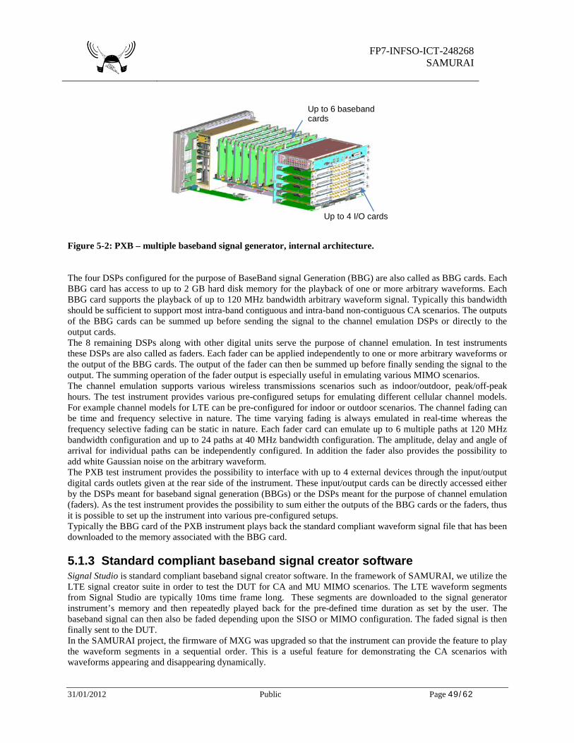
FP7-INFSO-ICT-248268
SAMURAI
31/01/2012 Public Page 49/62
Figure 5-2: PXB – multiple baseband signal generator, internal architecture. The four DSPs configured for the purpose of BaseBand signal Generation (BBG) are also called as BBG cards. Each BBG card has access to up to 2 GB hard disk memory for the playback of one or more arbitrary waveforms. Each BBG card supports the playback of up to 120 MHz bandwidth arbitrary waveform signal. Typically this bandwidth should be sufficient to support most intra-band contiguous and intra-band non-contiguous CA scenarios. The outputs of the BBG cards can be summed up before sending the signal to the channel emulation DSPs or directly to the output cards. The 8 remaining DSPs along with other digital units serve the purpose of channel emulation. In test instruments these DSPs are also called as faders. Each fader can be applied independently to one or more arbitrary waveforms or the output of the BBG cards. The output of the fader can then be summed up before finally sending the signal to the output. The summing operation of the fader output is especially useful in emulating various MIMO scenarios. The channel emulation supports various wireless transmissions scenarios such as indoor/outdoor, peak/off-peak hours. The test instrument provides various pre-configured setups for emulating different cellular channel models. For example channel models for LTE can be pre-configured for indoor or outdoor scenarios. The channel fading can be time and frequency selective in nature. The time varying fading is always emulated in real-time whereas the frequency selective fading can be static in nature. Each fader card can emulate up to 6 multiple paths at 120 MHz bandwidth configuration and up to 24 paths at 40 MHz bandwidth configuration. The amplitude, delay and angle of arrival for individual paths can be independently configured. In addition the fader also provides the possibility to add white Gaussian noise on the arbitrary waveform. The PXB test instrument provides the possibility to interface with up to 4 external devices through the input/output digital cards outlets given at the rear side of the instrument. These input/output cards can be directly accessed either by the DSPs meant for baseband signal generation (BBGs) or the DSPs meant for the purpose of channel emulation (faders). As the test instrument provides the possibility to sum either the outputs of the BBG cards or the faders, thus it is possible to set up the instrument into various pre-configured setups. Typically the BBG card of the PXB instrument plays back the standard compliant waveform signal file that has been downloaded to the memory associated with the BBG card.
5.1.3 Standard compliant baseband signal creator software Signal Studio is standard compliant baseband signal creator software. In the framework of SAMURAI, we utilize the LTE signal creator suite in order to test the DUT for CA and MU MIMO scenarios. The LTE waveform segments from Signal Studio are typically 10ms time frame long. These segments are downloaded to the signal generator instrument’s memory and then repeatedly played back for the pre-defined time duration as set by the user. The baseband signal can then also be faded depending upon the SISO or MIMO configuration. The faded signal is then finally sent to the DUT. In the SAMURAI project, the firmware of MXG was upgraded so that the instrument can provide the feature to play the waveform segments in a sequential order. This is a useful feature for demonstrating the CA scenarios with waveforms appearing and disappearing dynamically.
Up to 6 baseband cards
Up to 4 I/O cards
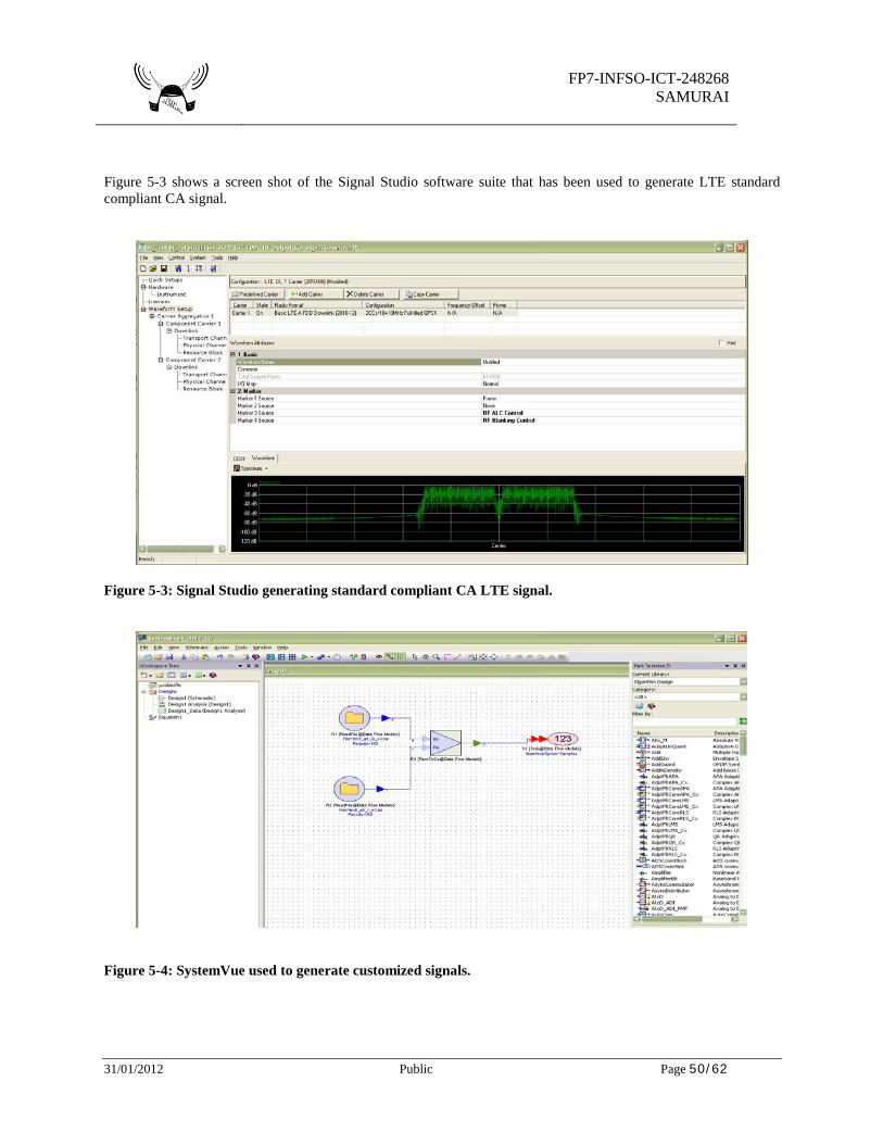
FP7-INFSO-ICT-248268
SAMURAI
31/01/2012 Public Page 50/62
Figure 5-3 shows a screen shot of the Signal Studio software suite that has been used to generate LTE standard compliant CA signal.
Figure 5-3: Signal Studio generating standard compliant CA LTE signal.
Figure 5-4: SystemVue used to generate customized signals.
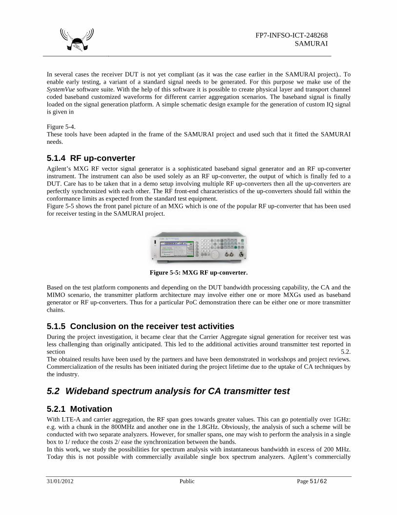
FP7-INFSO-ICT-248268
SAMURAI
31/01/2012 Public Page 51/62
In several cases the receiver DUT is not yet compliant (as it was the case earlier in the SAMURAI project).. To enable early testing, a variant of a standard signal needs to be generated. For this purpose we make use of the SystemVue software suite. With the help of this software it is possible to create physical layer and transport channel coded baseband customized waveforms for different carrier aggregation scenarios. The baseband signal is finally loaded on the signal generation platform. A simple schematic design example for the generation of custom IQ signal is given in Figure 5-4. These tools have been adapted in the frame of the SAMURAI project and used such that it fitted the SAMURAI needs.
5.1.4 RF up-converter Agilent’s MXG RF vector signal generator is a sophisticated baseband signal generator and an RF up-converter instrument. The instrument can also be used solely as an RF up-converter, the output of which is finally fed to a DUT. Care has to be taken that in a demo setup involving multiple RF up-converters then all the up-converters are perfectly synchronized with each other. The RF front-end characteristics of the up-converters should fall within the conformance limits as expected from the standard test equipment. Figure 5-5 shows the front panel picture of an MXG which is one of the popular RF up-converter that has been used for receiver testing in the SAMURAI project.
Figure 5-5: MXG RF up-converter.
Based on the test platform components and depending on the DUT bandwidth processing capability, the CA and the MIMO scenario, the transmitter platform architecture may involve either one or more MXGs used as baseband generator or RF up-converters. Thus for a particular PoC demonstration there can be either one or more transmitter chains.
5.1.5 Conclusion on the receiver test activities During the project investigation, it became clear that the Carrier Aggregate signal generation for receiver test was less challenging than originally anticipated. This led to the additional activities around transmitter test reported in section 5.2. The obtained results have been used by the partners and have been demonstrated in workshops and project reviews. Commercialization of the results has been initiated during the project lifetime due to the uptake of CA techniques by the industry.
5.2 Wideband spectrum analysis for CA transmitter test
5.2.1 Motivation With LTE-A and carrier aggregation, the RF span goes towards greater values. This can go potentially over 1GHz: e.g. with a chunk in the 800MHz and another one in the 1.8GHz. Obviously, the analysis of such a scheme will be conducted with two separate analyzers. However, for smaller spans, one may wish to perform the analysis in a single box to 1/ reduce the costs 2/ ease the synchronization between the bands. In this work, we study the possibilities for spectrum analysis with instantaneous bandwidth in excess of 200 MHz. Today this is not possible with commercially available single box spectrum analyzers. Agilent’s commercially
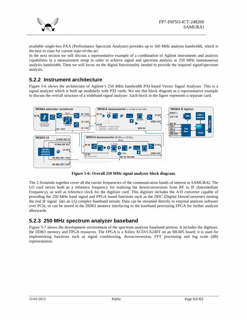
FP7-INFSO-ICT-248268
SAMURAI
31/01/2012 Public Page 52/62
available single-box PXA (Performance Spectrum Analyzer) provides up to 160 MHz analysis bandwidth, which is the best in class for current state-of-the-art. In the next section we will discuss a representative example of a combination of Agilent instruments and analysis capabilities in a measurement setup in order to achieve signal and spectrum analysis at 250 MHz instantaneous analysis bandwidth. Then we will focus on the digital functionality needed to provide the required signal/spectrum analysis.
5.2.2 Instrument architecture Figure 5-6 shows the architecture of Agilent’s 250 MHz bandwidth PXI-based Vector Signal Analyzer. This is a signal analyzer which is built up modularly with PXI cards. We use this block diagram as a representative example to discuss the overall structure of a wideband signal analyzer. Each block in the figure represents a separate card.
Figure 5-6: Overall 250 MHz signal analyzer block diagram.
The 2 frontends together cover all the carrier frequencies of the communication bands of interest to SAMURAI. The LO card serves both as a reference frequency for realizing the downconversions from RF to IF (Intermediate Frequency), as well as reference clock for the digitizer card. This digitizer includes the A/D converter capable of providing the 250 MHz band signal and FPGA based functions such as the DDC (Digital DownConverter) turning the real IF signal into an I,Q complex baseband stream. Data can be streamed directly to external analysis software over PCIe, or can be stored in the DDR3 memory interfacing to the baseband processing FPGA for further analysis afterwards.
5.2.3 250 MHz spectrum analyzer baseband Figure 5-7 shows the development environment of the spectrum analyzer baseband portion. It includes the digitizer, the DDR3 memory and FPGA resources. The FPGA is a Xilinx XC6VLX240T on an ML605 board; it is used for implementing functions such as signal conditioning, downconversion, FFT processing and log scale (dB) representation.
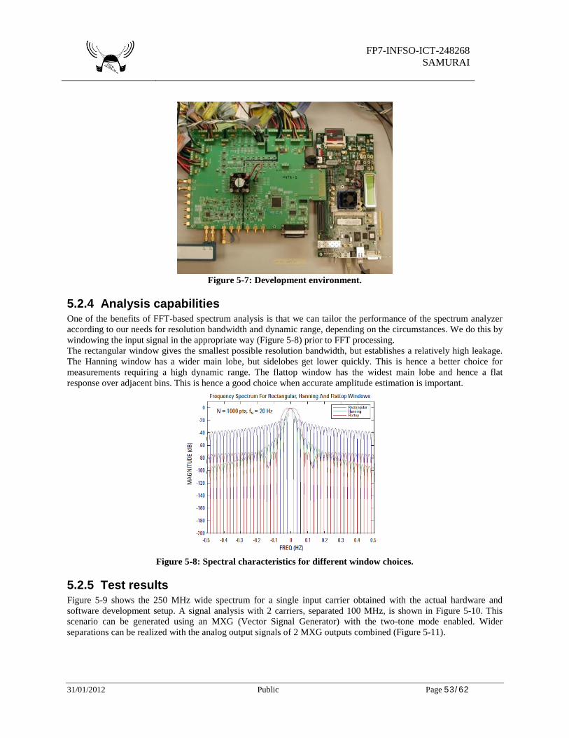
FP7-INFSO-ICT-248268
SAMURAI
31/01/2012 Public Page 53/62
Figure 5-7: Development environment.
5.2.4 Analysis capabilities One of the benefits of FFT-based spectrum analysis is that we can tailor the performance of the spectrum analyzer according to our needs for resolution bandwidth and dynamic range, depending on the circumstances. We do this by windowing the input signal in the appropriate way (Figure 5-8) prior to FFT processing. The rectangular window gives the smallest possible resolution bandwidth, but establishes a relatively high leakage. The Hanning window has a wider main lobe, but sidelobes get lower quickly. This is hence a better choice for measurements requiring a high dynamic range. The flattop window has the widest main lobe and hence a flat response over adjacent bins. This is hence a good choice when accurate amplitude estimation is important.
Figure 5-8: Spectral characteristics for different window choices.
5.2.5 Test results Figure 5-9 shows the 250 MHz wide spectrum for a single input carrier obtained with the actual hardware and software development setup. A signal analysis with 2 carriers, separated 100 MHz, is shown in Figure 5-10. This scenario can be generated using an MXG (Vector Signal Generator) with the two-tone mode enabled. Wider separations can be realized with the analog output signals of 2 MXG outputs combined (Figure 5-11).
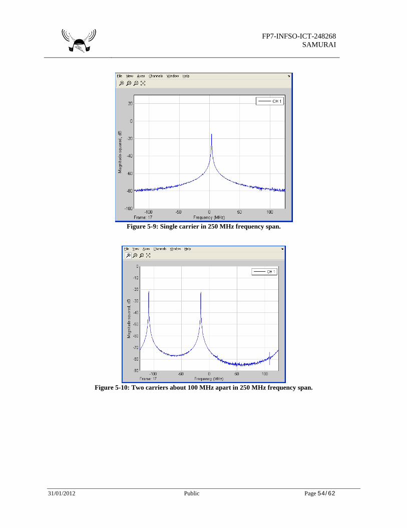
FP7-INFSO-ICT-248268
SAMURAI
31/01/2012 Public Page 54/62
Figure 5-9: Single carrier in 250 MHz frequency span.
Figure 5-10: Two carriers about 100 MHz apart in 250 MHz frequency span.
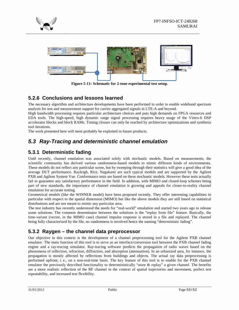
FP7-INFSO-ICT-248268
SAMURAI
31/01/2012 Public Page 55/62
Figure 5-11: Schematic for 2-tone experimental test setup.
5.2.6 Conclusions and lessons learned The necessary algorithm and architecture developments have been performed in order to enable wideband spectrum analysis for test and measurement support for carrier aggregated signals in LTE-A and beyond. High bandwidth processing requires particular architecture choices and puts high demands on FPGA resources and EDA tools. The high-speed, high dynamic range signal processing requires heavy usage of the Virtex-6 DSP accelerator blocks and block RAMs. Timing closure can only be reached by architecture optimizations and synthesis tool iterations. The work presented here will most probably be exploited in future products.
5.3 Ray-Tracing and deterministic channel emulation
5.3.1 Deterministic fading Until recently, channel emulation was associated solely with stochastic models. Based on measurements, the scientific community has derived various randomness-based models to mimic different kinds of environments. These models do not reflect any particular scene, but by sweeping through their statistics will give a good idea of the average DUT performance. Rayleigh, Rice, Nagakami are such typical models and are supported by the Agilent PXB and Agilent System Vue. Conformance tests are based on these stochastic models. However these tests actually fail to guarantee any satisfactory performance in the field. In addition, with MIMO and closed-loop schemes being part of new standards, the importance of channel emulation is growing and appeals for closer-to-reality channel emulation for accurate testing. Geometrical models (like the WINNER model) have been proposed recently. They offer interesting capabilities in particular with respect to the spatial dimension (MIMO) but like the above models they are still based on statistical distributions and are not meant to mimic any particular area. The test industry has recently understood the needs for “real-world” emulation and started two years ago to release some solutions. The common denominator between the solutions is the “replay from file” feature. Basically, the time-variant (vector, in the MIMO case) channel impulse response is stored in a file and replayed. The channel being fully characterized by the file, no randomness is involved hence the naming “deterministic fading”.
5.3.2 Raygen – the channel data preprocessor Our objective in this context is the development of a channel preprocessing tool for the Agilent PXB channel emulator. The main function of this tool is to serve as an interface/conversion tool between the PXB channel fading engine and a ray-tracing simulator. Ray-tracing software predicts the propagation of radio waves based on the phenomena of reflection, refraction, diffraction, and absorption (attenuation). In an urbanized area, for instance, the propagation is mostly affected by reflections from buildings and objects. The actual ray data preprocessing is performed upfront, i. e., on a non-real-time basis. The key feature of this tool is to enable for the PXB channel emulator the previously described functionality to deterministically “store & replay” a given channel. The benefits are a more realistic reflection of the RF channel in the context of spatial trajectories and movement, perfect test repeatability, and increased test flexibility.
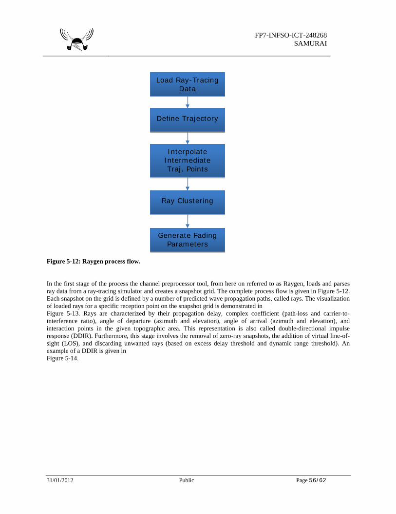
FP7-INFSO-ICT-248268
SAMURAI
31/01/2012 Public Page 56/62
Figure 5-12: Raygen process flow. In the first stage of the process the channel preprocessor tool, from here on referred to as Raygen, loads and parses ray data from a ray-tracing simulator and creates a snapshot grid. The complete process flow is given in Figure 5-12. Each snapshot on the grid is defined by a number of predicted wave propagation paths, called rays. The visualization of loaded rays for a specific reception point on the snapshot grid is demonstrated in Figure 5-13. Rays are characterized by their propagation delay, complex coefficient (path-loss and carrier-to-interference ratio), angle of departure (azimuth and elevation), angle of arrival (azimuth and elevation), and interaction points in the given topographic area. This representation is also called double-directional impulse response (DDIR). Furthermore, this stage involves the removal of zero-ray snapshots, the addition of virtual line-of-sight (LOS), and discarding unwanted rays (based on excess delay threshold and dynamic range threshold). An example of a DDIR is given in Figure 5-14.
Load Ray-Tracing Data
Define Trajectory
Interpolate Intermediate Traj. Points
Ray Clustering
Generate Fading Parameters
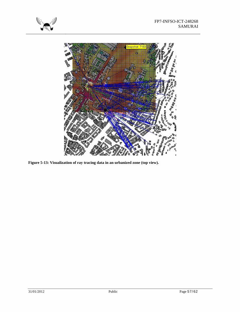
FP7-INFSO-ICT-248268
SAMURAI
31/01/2012 Public Page 57/62
Figure 5-13: Visualization of ray tracing data in an urbanized zone (top view).
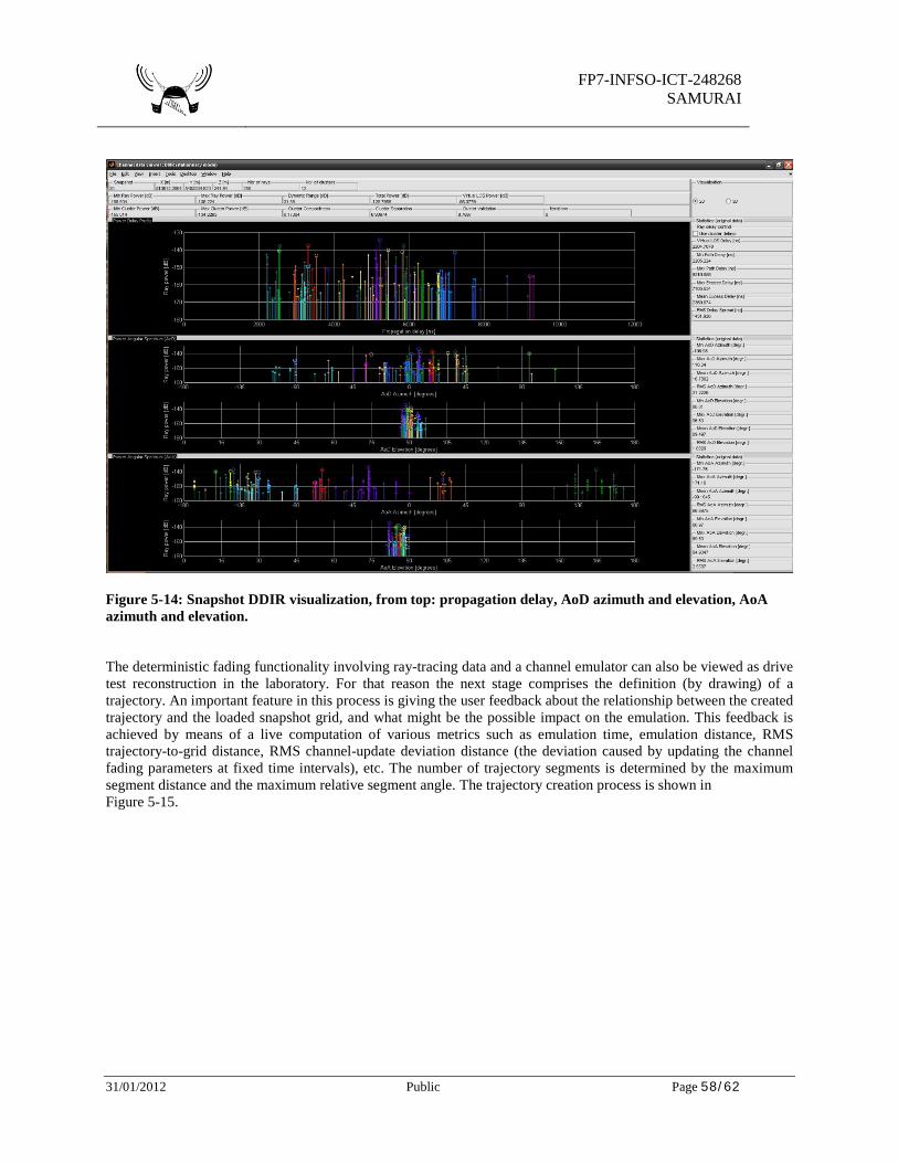
FP7-INFSO-ICT-248268
SAMURAI
31/01/2012 Public Page 58/62
Figure 5-14: Snapshot DDIR visualization, from top: propagation delay, AoD azimuth and elevation, AoA azimuth and elevation. The deterministic fading functionality involving ray-tracing data and a channel emulator can also be viewed as drive test reconstruction in the laboratory. For that reason the next stage comprises the definition (by drawing) of a trajectory. An important feature in this process is giving the user feedback about the relationship between the created trajectory and the loaded snapshot grid, and what might be the possible impact on the emulation. This feedback is achieved by means of a live computation of various metrics such as emulation time, emulation distance, RMS trajectory-to-grid distance, RMS channel-update deviation distance (the deviation caused by updating the channel fading parameters at fixed time intervals), etc. The number of trajectory segments is determined by the maximum segment distance and the maximum relative segment angle. The trajectory creation process is shown in Figure 5-15.
FP7-INFSO-ICT-248268
SAMURAI
31/01/2012 Public Page 59/62
Figure 5-15: Trajectory definition in the Raygen tool Wireless channel will vary in time based on the movement over a trajectory. Luckily, the fading parameters do not have to vary as fast as the signal sampling rate ( . In theory, the rate should be at least twice the maximum Doppler shift (Fd), nevertheless a higher update rate is generally recommended in practice. This shift is proportional to the speed of the mobile (v) and the carrier frequency (Fc) and defined as (c being the speed of light):
However, the update rate of fading parameters (in the sense of spatial movement) typically highly exceeds the density of the snapshot grid. Common snapshot grid density is 2-10 m. The obvious solution for this issue is the introduction of intermediate points to the trajectory segments and spatial interpolation of the channel parameters (DDIRs) at these points. For any two given neighboring snapshots on the trajectory we initiate a ray-to-ray mapping based on the multi-path component distances (MCD) between rays. MCD in this case depends on the inter-ray difference in AoA, delay, and power. The optimal assignment/mapping is achieved by the Hungarian algorithm (published by H. Kuhn, 1955). Since the sets of rays in snapshots are, in general, completely independent, a certain amount of rays will be too distant and will remain unmapped. Given the ray-to-ray mapping, the intermediate (artificial) snapshots will be created by inverse distance weighted interpolation of the two neighboring ray sets. Channel impulse response in the PXB is modeled using a tapped delay line implementation. Tapped delay line is a traditional technique for emulating a fading channel. In these models, each “tap” represents the sum of numerous multipath signals arriving at the same time. The tap amplitudes typically decrease over time as the signals arriving at later times have larger path loss and possibly undergo multiple reflections from the surrounding environment. PXB uses 24 taps in this model which is also the upper limit for distinct delayed paths that can be fed to the emulator from the Raygen tool. On the other hand, the number of rays per snapshot is normally higher (e. g., 256 rays). This difference triggers the need for clustering the rays in a snapshot into 24 (or less) clusters and eventually replacing the rays by their cluster-sum equivalent. The clustering is also based on MCD among rays in a particular snapshot.
FP7-INFSO-ICT-248268
SAMURAI
31/01/2012 Public Page 60/62
Nevertheless, the MCD definitions in these two stages might vary, since for optimal performance it may be necessary to adapt them (e. g. discarding power as a distance factor for clustering). The last stage of the process is the generation of fading parameters at the appropriate rate, saving them to a file, and uploading them to the channel emulator. Given DDIRs for all points (including the interpolated intermediate ones) on a trajectory, we translate the Tx and Rx antenna offsets and extract a set of ray descriptors for each MIMO branch for all the points. Besides ray delay, magnitude, and phase, the ray descriptors include also the ray Doppler shift parameter. In the next step the ray descriptors are converted to so-called path descriptors, which means the incorporation of the ray Doppler shift into the path (I,Q) coefficients and upsampling to the required PXB-channel-update rate. The last task is to perform (ray/)path descriptor recombination according to obtained ray-cluster assignment. The channel fading requirements on the memory storage can be easily computed as follows:
M and N are the numbers of Tx and Rx antennas, respectively, 24 is the number of filter taps in the PXB, and 16 bytes is the assumed size of one path descriptor. K is the oversampling factor with respect to the max Doppler (frequency) shift Fd. Assuming a MIMO 2x2 system, at a carrier frequency of 1.8GHz, a UE moving at 30m/s and an oversampling factor of 24, this gives a storage requirement of 6.64MB/s, i.e., 1GB for 150 seconds of emulation. The update rate of path descriptors in this example is 4.32 kHz, which is typically much less than the transmission sampling rate.
5.3.3 Conclusions and lessons learned A software pre-processor able to convert deterministic data into a readable format for the PXB channel emulator has been developed. The work done in the frame of SAMURAI will enable the reproducibility of any MIMO channel taking into account its spatial component. This work was used in measurement campaign done in cooperation with Eurecom and demonstrated at the FuNems conference (see figure in section 4.3). The limitation of the current platform have been identified and documented for a possible future upgrade. Agilent intends to exploit the result in products in the next years.
FP7-INFSO-ICT-248268
SAMURAI
31/01/2012 Public Page 61/62
6 Feedback to WP2 In order to provide solidity to the results presented in the project, a feedback from the development experience to the simulation environment is needed. In particular, within the framework of the project it has been possible to provide a feedback about the evaluation of the ACCS algorithm. The ACCS test bed has been used for this purpose, not only for running the full ACCS algorithm as presented in this deliverable, but also as a multi-node channel sounder. Thanks to the simple physical layer, that exploits fully orthogonal transmissions among the nodes, it has been possible to estimate the pathloss between each pair of nodes, independently to which network role (eNB or UE) they could have. This pathloss matrix has been used as an input to the ACCS light simulator, in order to re-create in the simulator the environmental conditions experienced by the test-bed. Furthermore, such pathloss matrix has been acquired periodically in time, in order to provide time snapshots for following the variations of the channel that could be experienced in a dynamic environment such as a used office-indoor situation. The results of such studies, comparing the different experiences (fully simulated with channel model, simulated based on real pathloss, live experience), will be presented in D2.3 in order to wrap up the lessons learned in this field within the SAMURAI project.
FP7-INFSO-ICT-248268
SAMURAI
31/01/2012 Public Page 62/62
7 References [1] 3GPP TR36.211, Technical Specification Group Radio Access Network; “Evolved Universal
Terrestrial Radio Access (E-UTRA); `Physical Channels and Modulation (Release 8)'', v8.6.0, Sep 2009.
[2] 3GPP TS 36.212 Technical Specification Group Radio Access Network, "Evolved Universal Terrestrial Radio Access (E-UTRA); Multiplexing and Channel Coding (Release 8)”, v8.6.0, Sep 2009.
[3] 3GPP TS 36.213 Technical Specification Group Radio Access Network, "Evolved Universal Terrestrial Radio Access (E-UTRA); Physical layer procedures (Release 8)", v8.6.0, Sep 2009;
[4] 3GPP TS 36.321 Technical Specification Group Radio Access Network; Evolved Universal Terrestrial Radio Access (E-UTRA) Medium Access Control (MAC) protocol specification (Release 8), v8.6.0, Sep 2009
[5] FP7-INFSO-ICT-248268 SAMURAI – Work Package 5, " D5.1 Proof-of-concepts definition", December 2010.
[6] FP7-INFSO-ICT-248993 LOLA – Work Package 5, “D 5.2 First report on Integration of WP3 Traffic Models and WP4 L2 Algorithms on Testbed 1”, December 2012
[7] Jonathan Duplicy, Biljana Badic, Rajarajan Balraj, Rizwan Ghaffar, Péter Horváth, Florian Kaltenberger, Raymond Knopp, István Z. Kovács, Hung T. Nguyen, Deepaknath Tandur and Guillaume Vivier, "MU-MIMO in LTE Systems", EURASIP Journal on Wireless Communications and Networking, vol. 2011, Article ID 496763, 13 pages, 2011. doi:10.1155/2011/496763.
[8] Ghaffar, Rizwan; Knopp, Raymond, "Interference-aware receiver structure for Multi-User MIMO and LTE", EURASIP Journal on Wireless Communications and Networking, Volume 2011: 40.
[9] Guangxiang Y. et al., "Carrier Aggregation for LTE.ADVANCED Mobile Communication Systems", IEEE Communications Magazine, February 2010, pp. 88 – 93.
[10] Luis G. U. Garcia, et al., "Autonomous Component Carrier Selection: Interference Management in Local Area Environments forLTE.ADVANCED", IEEE Communications Magazine, September 2009, pp. 110 – 116.
[11] FP7-INFSO-ICT-ACROPOLIS – Work Package 5, “D5.2: Report on the Analysis of OpenAirInterface and its Distribution in Consortium”, September 2012.
Documentation of dlsim.c
Sebastian Wagner
September 20, 2012
1 Introduction
This document provides a detailed description of the dlsim.c simulation setup.Particular attention is payed to explain the transition from communication the-ory to the actual implementation of the physical layer.
The dlsim is a link-level downlink simulation script of the OpenAirInterface(OAI) which implements the 3GPP LTE Release 8.6 wireless communicationstandard.
2 Fixed-point Arithmetic
The algorithms used for the OAI are implemented in fixed-point (FXP) arith-metic. FXP arithmetic can usually be much more efficiently implemented inhard-ware and is therefore preferred over floating-point (FLP) arithmetic. Asindicated by the name, any number a represented with n bits in FXP format hasa static (fixed) binary point, i.e., a fixed number of bits before the binary point(magnitude bits) and after the binary point (fractional bits). In the followingwe adhere to the “Q” notation, i.e., the format Qm.f indicates that the FXPnumber has m magnitude bits and f fractional bits. For instance, a 16 bit num-ber a represented in Q3.13 format has 3 magnitude bits and 13 fractional bits.Thus if a is a signed integer, then 2 bits are left for the magnitude and hencea ∈ [−5, ..., 4]. In the implementation, the format Q1.15 is most commonly usedwhich can represent numbers between -1 and 1.
To transform a real number a ∈ [0, 1] into a n-bit unsigned integer, we scaleit by 2n. If a ∈ [−1, 1] you scale by 2n−1 since the first bit is the sign bit.
afxp = ba · 2n−1c. (1)
2.1 Arithmetic
First, we consider addition and subtraction of two FXP numbers Qm1.f1 andQm2.f2. In both cases, the result must be represented in the format Q(m1 +m2), f . That is, the result may lead to a saturation. Therefore, it has to beassured that the result can never exceed the range of values.
1

The multiplication of two FXP number yields
Qm1.f1 ·Qm2.f2 = Q(m1 +m2).(f1 + f2).
That is, multiplying two 16bit number yields a 32bit result. To obtain a 16bitvalue, the result has to be shifted to the right.
2

3 Receiver Design
In this section, we describe the receiver design implemented in the OAI.
3.1 ML Receiver
We consider M independent complex symbols s ∈ QM , |QM | = M , drawn fromthe symbol alphabet QM . Thus a symbol by symbol detection is optimal.
3.2 AWGN
First, we consider the case of a single transmit antenna and a single receiveantenna. Hence the received symbol y is given by
y = s+ n, (2)
where n ∈ CN (0, σ2) is the additive complex Gaussian noise.The goal is to maximize the probability of correct detection, i.e., the prob-
ability that symbol s has been transmitted given the received symbol y, whichis defined as the posterior probability
P (s|y), s ∈ QM . (3)
The most likely send symbol thus corresponds to the maximum of all possibleposterior probabilities, i.e.,
s = arg maxs∈QM
{P (s|y)}. (4)
This detection rule is referred to as maximum a posteriori probability (MAP)criterion. Applying Bayes’ rule to (3), we obtain
P (s|y) =p(y|s)P (s)
p(y), (5)
where p(y|s) is conditional probability of y given symbol s ∈ QM has beentransmitted and P (s) is the probability that s has been transmitted, thus P (s)is called a priori probability of s.
Note that we write a capital P (x) is the probabilities are discrete and p(x)if it is continuous.
Since the denominator of (5) can be written as p(y) =∑Mi=1 p(y|s)P (s), the
posterior probabilities P (s|y) are solely dependent on the conditional probabil-ities p(y|s) and the a priori probabilities P (s). In any case, the probability p(y)is identical for all symbols s ∈ QM and thus doesn’t affect the MAP criterionin (4).
However, a significant simplification occurs if the symbols s are equally likely,i.e., P (s) = 1
M ∀M, s ∈ QM . In this case the MAP criterion reduces to finding
3
the maximum conditional probabilities p(y|s) or any monotonic function f(x)thereof, i.e.,
s = arg maxs∈QM
{f(p(y|s))}. (6)
The function f(p(y|s)) is often called likelihood function and thus the detectioncriterion in (6) is referred to as maximum-likelihood (ML) criterion. Note thatthe assumption of equally likely symbols is justified since in practical systemthe bits to be transmitted are often randomized by scrambling and interleav-ing operations before they are mapped onto the symbols. This randomizationyields (among other advantages) a approximately uniform distribution of thebit stream.
Consequently, the MAP and ML criterion are equivalent, if the transmittedsymbols are equally likely.
The probability distribution function (pdf) p(z) of a N -dimensional circularsymmetric complex Gaussian vector z is given by
p(z) =1
πN det(C)exp
(−(z−m)HC−1(z−m)
), (7)
where m = E[z] and C = E[(z−m)(z−m)H]. Since the noise term n is circularsymmetric complex Gaussian, the conditional probability p(y|s) is given by (7)for N = 1, where
m = m = E[y|s] = E[s+ n|s] = E[s|s] + E[n|s] = s, (8)
where E[s|s] = s since E[s|s] is the expected transmit symbol s given thats ∈ QM has been transmitted and E[n|s] = E[n] = 0, because n is independentof s. We further have
C = C = E[(y − s|s)(y − s|s)H] = E[(s+ n− s|s)(s+ n− s|s)H] (9)
= E[ssH + nnH + ssH + 2snH − 2ssH +−2nsH|s] (10)
= E[ssH] + E[nnH] + E[ssH]− 2E[ssH] (11)
= E[nnH] = σ2. (12)
Therefore, p(y|s) takes the form
p(y|s) =1πσ2
exp(− 1σ2
(y − s)H(y − s)). (13)
To simplify the calculation we choose the likelihood function f(x) = ln(x) andthis we have
ln p(y|s) = − ln(πσ2)− 1σ2|y − s|2. (14)
The detection criterion in (6) thus simplifies to
s = arg mins∈QM
{|y − s|2}. (15)
4
That is, the most likely transmitted symbol s is given by the symbol withthe minimum (squared) euclidean distance from the received symbol y. Thedistance D(y, s) = |y− s|2 can be further simplified by expanding the quadraticterm
D(y, s) = (<(y)−<(s))2 + (=(y)−=(s))2 (16)
= −2<(y)<(s)− 2=(y)=(s) + |y|2 + |s|2. (17)
Define the minimum distance as
λ(y, s) , mins∈QM
D(y, s) = maxs∈QM
−D(y, s). (18)
The term |y|2 is common for all D(y, s) and can thus be omitted in the compu-tation of λ(y, s), we obtain
λ(y, s) = maxs∈QM
{2<(y)<(s) + 2=(y)=(s)− |s|2
}, (19)
where |s|2 is the power of the ith symbol which depends on the alphabet QM ,e.g, |s|2 = 1 for all symbols of a normalized QPSK constellation. For 16QAMwe have |s|2 = { 2
10 ,1010 ,
1810}.
A decision rule about weather s or sk as been transmitted can be defined asthe logarithm of the conditional pdfs denoted Λ(y), i.e.,
Λ(y) = ln(p(y|s)p(y|sk)
)= ln
(exp
(− 1σ2 |y − s|2
)exp
(− 1σ2 |y − sk|2
)) . (20)
The term Λ(y) is called log likelihood ratio and is zero if s = sk and greaterthan zero if s is more likely of having been transmitted. However, if channelcoding is implemented in the communication system, the channel decoder ofterrequires some measure of how likely a certain bit is either 0 or 1. This measureis the likelihood ratio of the conditional pdfs, i.e.,
Λ(y|s(bk)) = ln(p(y|bk = 1)p(y|bk = 0)
)= ln
(∑s∈QM (bk=1) exp
(− 1σ2 |y − s|2
)∑s∈QM (bk=0) exp
(− 1σ2 |y − s|2
)) . (21)
The magnitude of the LLR is associated with the reliability of the decision. Sincethe function exp(−x) is decreasing rapidly for increasing x, we observe, that forlow noise power σ2, i.e., high SNR, the values in the exponent become smallerand therefore a slight increase in the argument x can result in a significantchange in exp(−x). Hence, the smallest term in the sums tends to dominateall remaining terms in the sum. Therefore, we might neglect the small termsand only consider the dominant term. This approximation is called MaxLog
5
approximation and the resulting LLR is given by
Λ(y|s(bk)) ≈ ln
(maxs∈QM (bk=1) exp
(− 1σ2 |y − s|2
)maxs∈QM (bk=0) exp
(− 1σ2 |y − s|2
)) (22)
= maxs∈QM (bk=0)
{− 1σ2|y − s|2
}−{
maxs∈QM (bk=1)
− 1σ2|y − s|2
}(23)
Λ(y|s(bk)) =1σ2
[λ(y|s(bk = 1))− λ(y|s(bk = 0))] (24)> 0 → bk = 1= 0 → bk = 0 or 1< 0 → bk = 0.
(25)
The scaling term 1σ2 is common to all LLRs and we omit it in the following.
Moreover, since we implement a Maxlog turbo decoder, it is not necessary toscale the LLRs with the noise variance. This has the advantage that we don’tneed to estimate the noise variance. However for a good noise variance estimatethe real turbo decoder performs slightly better, also for a bad noise variance itmight perform worse that the Maxlog turbo decoder.
3.3 SISO
This discussion in the AWGN case extends in a straight-forward manner to theSISO flat-fading case where h ∈ C is the channel coefficient. Usually some esti-mate h of h is known to the transmitter. Assuming perfect channel estimation,i.e., h = h, we can simply replace s with hs in the distance computation. Aftersome algebraic manipulation, we obtain
λ(y, h, s) = maxs∈QM
{2<(y)<(s) + 2=(y)=(s)− |h|2<(s)2 − |h|2=(s)2
}, (26)
where y = hHy is the received signal after matched filtering. Subsequentlywe will write λ(bk = 1) , λ(y, h, s), s ∈ QM (bk = 1). Using the MaxLogapproximation, the LLR of bit k are thus given by
Λk = λ(bk = 1)− λ(bk = 0). (27)
Grouping the maximization in (3) into real and imaginary part of s we obtain
Λk = (28)
maxs∈QM (bk=1)
{2<(y)<(s)− |h|2<(s)2
}+ maxs∈QM (bk=1)
{2=(y)=(s)− |h|2=(s)2
}− maxs∈QM (bk=0)
{2<(y)<(s)− |h|2<(s)2
}− maxs∈QM (bk=0)
{2=(y)=(s)− |h|2=(s)2
}.
(29)
Now, given the LTE symbol constellation, we observe that for the odd bits bk,k ∈ {1, 3, 5}, only the maximization of over the real parts of s count because
6
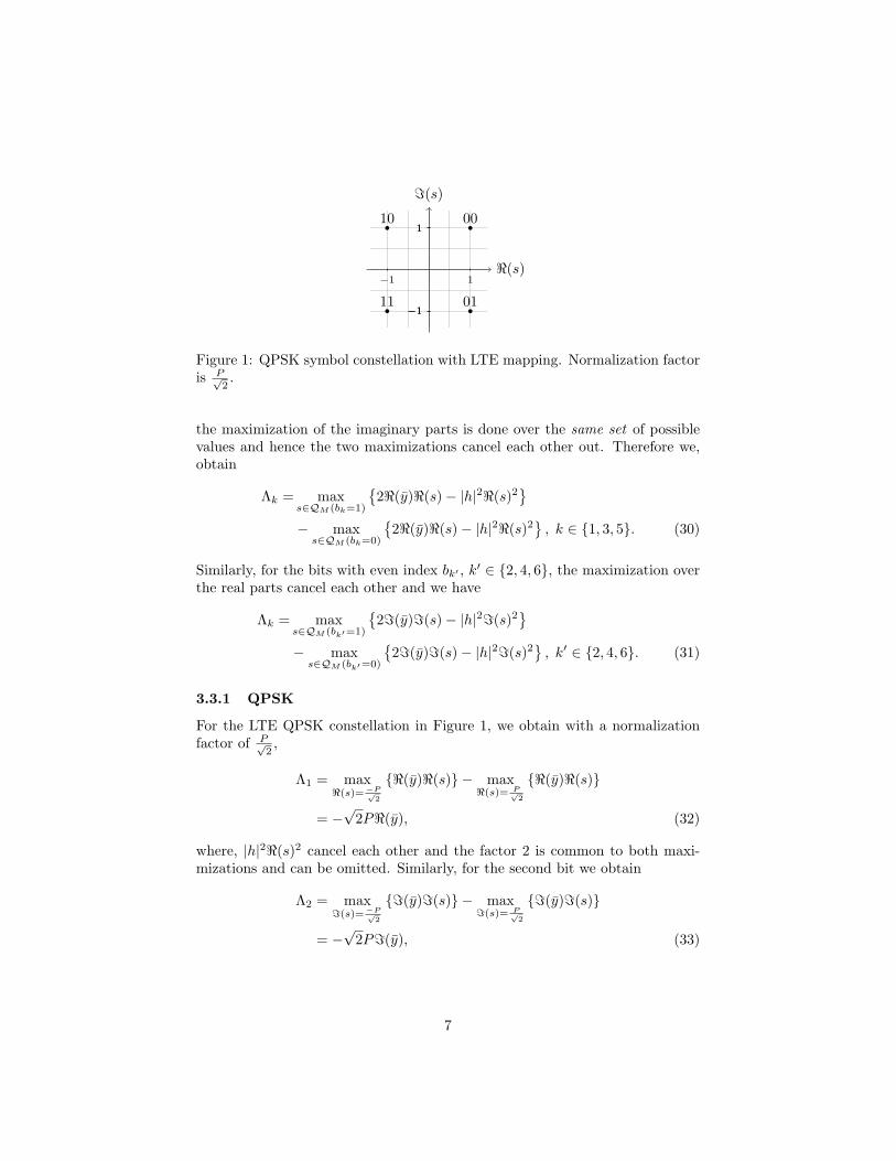
<(s)
=(s)
−1
−1
1
1
−1
100
01
10
11
Figure 1: QPSK symbol constellation with LTE mapping. Normalization factoris P√
2.
the maximization of the imaginary parts is done over the same set of possiblevalues and hence the two maximizations cancel each other out. Therefore we,obtain
Λk = maxs∈QM (bk=1)
{2<(y)<(s)− |h|2<(s)2
}− maxs∈QM (bk=0)
{2<(y)<(s)− |h|2<(s)2
}, k ∈ {1, 3, 5}. (30)
Similarly, for the bits with even index bk′ , k′ ∈ {2, 4, 6}, the maximization overthe real parts cancel each other and we have
Λk = maxs∈QM (bk′=1)
{2=(y)=(s)− |h|2=(s)2
}− maxs∈QM (bk′=0)
{2=(y)=(s)− |h|2=(s)2
}, k′ ∈ {2, 4, 6}. (31)
3.3.1 QPSK
For the LTE QPSK constellation in Figure 1, we obtain with a normalizationfactor of P√
2,
Λ1 = max<(s)=−P√
2
{<(y)<(s)} − max<(s)= P√
2
{<(y)<(s)}
= −√
2P<(y), (32)
where, |h|2<(s)2 cancel each other and the factor 2 is common to both maxi-mizations and can be omitted. Similarly, for the second bit we obtain
Λ2 = max=(s)=−P√
2
{=(y)=(s)} − max=(s)= P√
2
{=(y)=(s)}
= −√
2P=(y), (33)
7
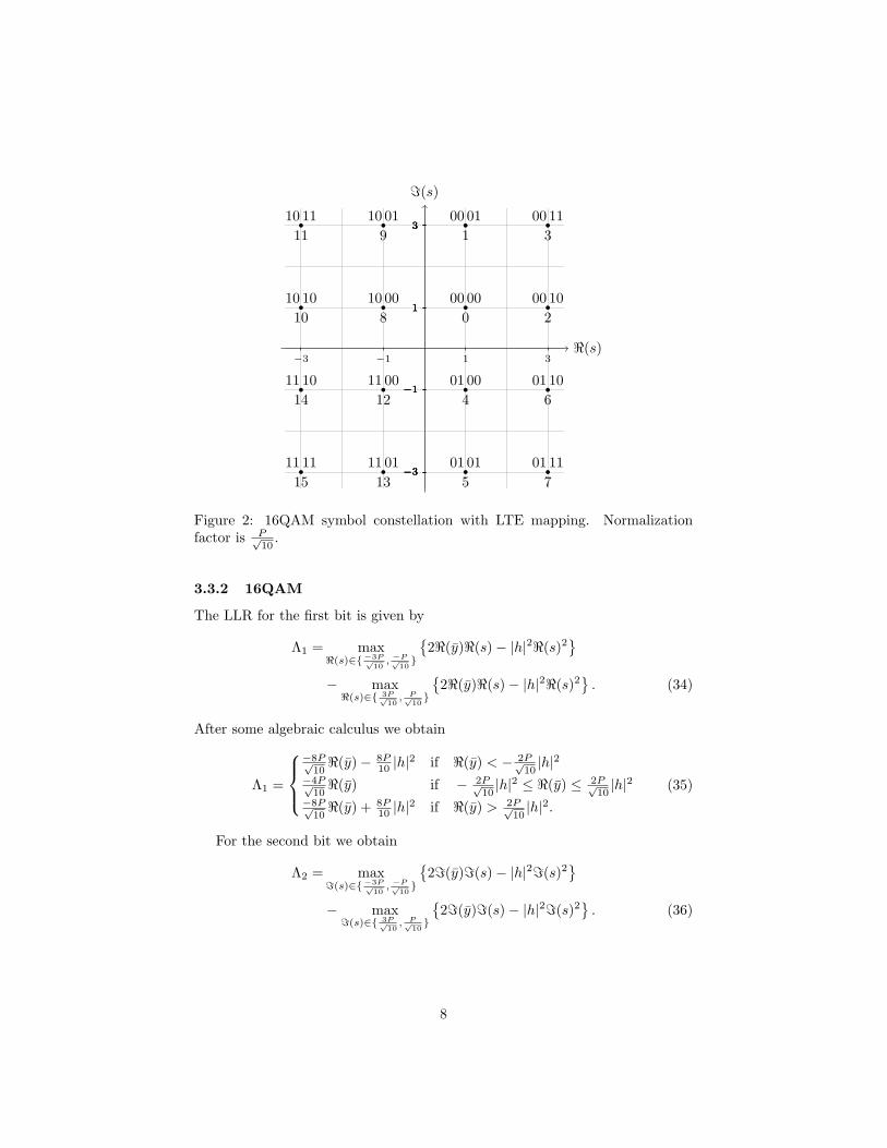
<(s)
=(s)
−3
−3
−1
1
3
−1
−3
−1
1
3
1
−3
−1
1
3
3
−3
−1
1
3
00 000
00 011
00 102
00 113
01 004
01 015
01 106
01 117
11 0012
11 0113
11 1014
11 1115
10 008
10 019
10 1010
10 1111
Figure 2: 16QAM symbol constellation with LTE mapping. Normalizationfactor is P√
10.
3.3.2 16QAM
The LLR for the first bit is given by
Λ1 = max<(s)∈{−3P√
10, −P√
10}
{2<(y)<(s)− |h|2<(s)2
}− max<(s)∈{ 3P√
10, P√
10}
{2<(y)<(s)− |h|2<(s)2
}. (34)
After some algebraic calculus we obtain
Λ1 =
−8P√
10<(y)− 8P
10 |h|2 if <(y) < − 2P√
10|h|2
−4P√10<(y) if − 2P√
10|h|2 ≤ <(y) ≤ 2P√
10|h|2
−8P√10<(y) + 8P
10 |h|2 if <(y) > 2P√
10|h|2.
(35)
For the second bit we obtain
Λ2 = max=(s)∈{−3P√
10, −P√
10}
{2=(y)=(s)− |h|2=(s)2
}− max=(s)∈{ 3P√
10, P√
10}
{2=(y)=(s)− |h|2=(s)2
}. (36)
8
This is similar to Λ1 except that we have to replace <(y) by =(y) and obtain
Λ2 =
−8P√
10=(y)− 8P
10 |h|2 if =(y) < − 2P√
10|h|2
−4P√10=(y) if − 2P√
10|h|2 ≤ =(y) ≤ 2P√
10|h|2
−8P√10=(y) + 8P
10 |h|2 if =(y) > 2P√
10|h|2
(37)
(38)
The LLR of the third bit is computed as
Λ3 = max<(s)∈{−3P√
10, 3P√
10}
{2<(y)<(s)− |h|2<(s)2
}− max<(s)∈{ −P√
10, P√
10}
{2<(y)<(s)− |h|2<(s)2
}(39)
which is given by
Λ3 =4P√
10|<(y)| − 8P 2
10|h|2. (40)
Finally, the LLR of the fourth but is given by
Λ4 = max=(s)∈{−3P√
10, 3P√
10}
{2=(y)=(s)− |h|2=(s)2
}− max=(s)∈{ −P√
10, P√
10}
{2=(y)=(s)− |h|2=(s)2
}(41)
and reads
Λ4 =4P√
10|=(y)| − 8P 2
10|h|2. (42)
Observe, that only the LLR of the two most significant bits (bits 1 and 2)is approximated whereas the LLRs of the less significant bits are exact. Thus,the approximation is justified since the first to bits are well protected and errorscan be more easily tolerated.
9
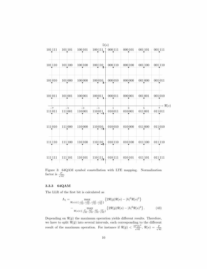
<(s)
=(s)
−7
−7
−5
−3
−1
1
3
5
7
−5
−7
−5
−3
−1
1
3
5
7
−3
−7
−5
−3
−1
1
3
5
7
−1
−7
−5
−3
−1
1
3
5
7
1
−7
−5
−3
−1
1
3
5
7
3
−7
−5
−3
−1
1
3
5
7
5
−7
−5
−3
−1
1
3
5
7
7
−7
−5
−3
−1
1
3
5
7
000 011
000 010
000 001
000 000
000 110
000 111
000 100
000 101
001 001
001 000
001 010
001 011
001 100
001 101
001 110
001 111
010 011
010 010
010 001
010 000
010 110
010 111
010 100
010 101
011 001
011 000
011 011
011 010
011 100
011 101
011 110
011 111
110 011
110 010
110 001
110 000
110 110
110 111
110 100
110 101
111 100
111 101
111 110
111 111
111 001
111 000
111 011
111 010
100 011
100 010
100 001
100 000
100 110
100 111
100 100
100 101
101 100
101 101
101 110
101 111
101 001
101 000
101 011
101 010
Figure 3: 64QAM symbol constellation with LTE mapping. Normalizationfactor is P√
42.
3.3.3 64QAM
The LLR of the first bit is calculated as
Λ1 = max<(s)∈{ −P√
42,−3P√
42,−5P√
42,−7P√
42}
{2<(y)<(s)− |h|2<(s)2
}− max<(s)∈{ P√
42, 3P√
42, 5P√
42, 7P√
42}
{2<(y)<(s)− |h|2<(s)2
}. (43)
Depending on <(y) the maximum operation yields different results. Therefore,we have to split <(y) into several intervals, each corresponding to the differentresult of the maximum operation. For instance if <(y) < 2P |h|2√
42, <(s) = P√
42
10
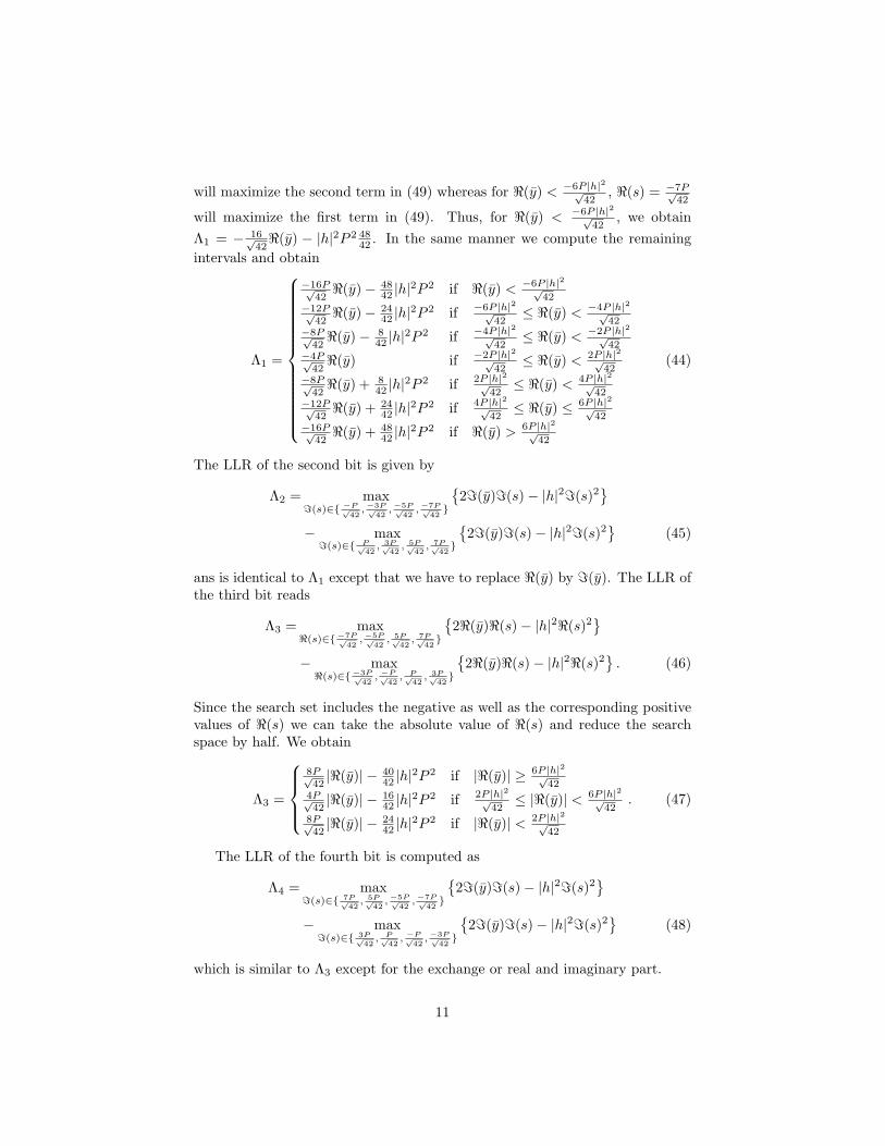
will maximize the second term in (49) whereas for <(y) < −6P |h|2√42
, <(s) = −7P√42
will maximize the first term in (49). Thus, for <(y) < −6P |h|2√42
, we obtainΛ1 = − 16√
42<(y) − |h|2P 2 48
42 . In the same manner we compute the remainingintervals and obtain
Λ1 =
−16P√42<(y)− 48
42 |h|2P 2 if <(y) < −6P |h|2√
42−12P√
42<(y)− 24
42 |h|2P 2 if −6P |h|2√
42≤ <(y) < −4P |h|2√
42−8P√
42<(y)− 8
42 |h|2P 2 if −4P |h|2√
42≤ <(y) < −2P |h|2√
42−4P√
42<(y) if −2P |h|2√
42≤ <(y) < 2P |h|2√
42−8P√
42<(y) + 8
42 |h|2P 2 if 2P |h|2√
42≤ <(y) < 4P |h|2√
42−12P√
42<(y) + 24
42 |h|2P 2 if 4P |h|2√
42≤ <(y) ≤ 6P |h|2√
42−16P√
42<(y) + 48
42 |h|2P 2 if <(y) > 6P |h|2√
42
(44)
The LLR of the second bit is given by
Λ2 = max=(s)∈{ −P√
42,−3P√
42,−5P√
42,−7P√
42}
{2=(y)=(s)− |h|2=(s)2
}− max=(s)∈{ P√
42, 3P√
42, 5P√
42, 7P√
42}
{2=(y)=(s)− |h|2=(s)2
}(45)
ans is identical to Λ1 except that we have to replace <(y) by =(y). The LLR ofthe third bit reads
Λ3 = max<(s)∈{−7P√
42,−5P√
42, 5P√
42, 7P√
42}
{2<(y)<(s)− |h|2<(s)2
}− max<(s)∈{−3P√
42, −P√
42, P√
42, 3P√
42}
{2<(y)<(s)− |h|2<(s)2
}. (46)
Since the search set includes the negative as well as the corresponding positivevalues of <(s) we can take the absolute value of <(s) and reduce the searchspace by half. We obtain
Λ3 =
8P√42|<(y)| − 40
42 |h|2P 2 if |<(y)| ≥ 6P |h|2√
424P√42|<(y)| − 16
42 |h|2P 2 if 2P |h|2√
42≤ |<(y)| < 6P |h|2√
428P√42|<(y)| − 24
42 |h|2P 2 if |<(y)| < 2P |h|2√
42
. (47)
The LLR of the fourth bit is computed as
Λ4 = max=(s)∈{ 7P√
42, 5P√
42,−5P√
42,−7P√
42}
{2=(y)=(s)− |h|2=(s)2
}− max=(s)∈{ 3P√
42, P√
42, −P√
42,−3P√
42}
{2=(y)=(s)− |h|2=(s)2
}(48)
which is similar to Λ3 except for the exchange or real and imaginary part.
11
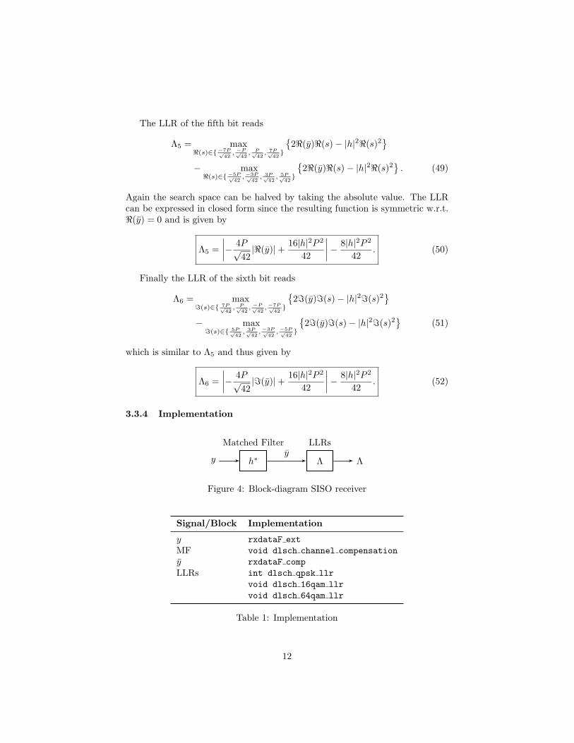
The LLR of the fifth bit reads
Λ5 = max<(s)∈{−7P√
42, −P√
42, P√
42, 7P√
42}
{2<(y)<(s)− |h|2<(s)2
}− max<(s)∈{−5P√
42,−3P√
42, 3P√
42, 5P√
42}
{2<(y)<(s)− |h|2<(s)2
}. (49)
Again the search space can be halved by taking the absolute value. The LLRcan be expressed in closed form since the resulting function is symmetric w.r.t.<(y) = 0 and is given by
Λ5 =∣∣∣∣− 4P√
42|<(y)|+ 16|h|2P 2
42
∣∣∣∣− 8|h|2P 2
42. (50)
Finally the LLR of the sixth bit reads
Λ6 = max=(s)∈{ 7P√
42, P√
42, −P√
42,−7P√
42}
{2=(y)=(s)− |h|2=(s)2
}− max=(s)∈{ 5P√
42, 3P√
42,−3P√
42,−5P√
42}
{2=(y)=(s)− |h|2=(s)2
}(51)
which is similar to Λ5 and thus given by
Λ6 =∣∣∣∣− 4P√
42|=(y)|+ 16|h|2P 2
42
∣∣∣∣− 8|h|2P 2
42. (52)
3.3.4 Implementation
y h∗ Λ Λ
Matched Filter LLRsy
Figure 4: Block-diagram SISO receiver
Signal/Block Implementation
y rxdataF extMF void dlsch channel compensationy rxdataF compLLRs int dlsch qpsk llr
void dlsch 16qam llrvoid dlsch 64qam llr
Table 1: Implementation
12
From an implementation point of view, it is undesirable to carry out thresh-old checking to compute the LLRs, like for Λ1,Λ2 in case of both 16-QAM andand 64-QAM. Different approximation can be introduced to make the imple-mentation more efficient. First we could average over all intervals assumingthat each interval is equally likely, which is approximately true for Rayleigh-fading channels. We obtain
Λ1 ≈
{−20P3√
10<(y) if 16QAM
−767√
42<(y) if 64QAM
(53)
Λ2 ≈
{−20P3√
10=(y) if 16QAM
−767√
42=(y) if 64QAM.
(54)
This approximation avoids the difficulty of threshold testing. A disadvantage isthat even after eliminating the common scaling factor e.g. for 16QAM 4P√
10, the
LLRs still involve the multiplication by a factor 53 . This multiplication can be
avoided by considering only the middle interval, i.e.
Λ1 ≈
{−4P√
10<(y) if 16QAM
−4P√42<(y) if 64QAM
(55)
Λ2 ≈
{−4P√
10=(y) if 16QAM
−4P√42=(y) if 64QAM.
(56)
After omitting the common scaling term 4P√10
and setting P = 1, the LLRs for16QAM read
Λ1 ≈ −<(y) (57)Λ2 ≈ −=(y) (58)
Λ3 = |<(y)| − 2√10|h|2 (59)
Λ4 = |=(y)| − 2√10|h|2. (60)
For 64QAM we have
Λ1 ≈ −<(y) (61)Λ2 ≈ −=(y) (62)
Λ3 = |<(y)| − 4√42|h|2 (63)
Λ4 = |=(y)| − 4√42|h|2 (64)
Λ5 =∣∣∣∣−|<(y)|+ 4|h|2√
42
∣∣∣∣− 2|h|2
42(65)
Λ6 =∣∣∣∣−|=(y)|+ 4|h|2√
42
∣∣∣∣− 2|h|2
42. (66)
13

Note also that this approximation are done for the most significant bits, whichenjoy a high error protection. Thus, the two different approximations presentedhere will most likely result in almost identical performance.
14
3.4 SU-MIMO
Consider an nt-antenna transmitter communicating to a single user equippedwith nr antennas. For flat-fading channels the received signal y = [y0, y1, . . . , ynr−1]T
is given by1
y = Hs + n =nr−1∑k=0
hksk + n, (67)
where H = [h0,h1, . . . ,hnt−1] ∈ Cnr×nt is the compound channel matrix withhk representing the channel from the transmit antenna array to the kth receiveantenna, s = [s0, s1, . . . , snr−1]T is the symbol vector and n = [n0, n1, . . . , nnr−1]is the noise vector with nk ∈ CN (0, σ2). The symbols sk ∈ Ak drawn from thesymbol alphabet Ak have average power E[sks∗k] = Pk. The channel matrix isdefined as
H =
h0,0 h1,0 · · · hnt−1,0
h0,1 h1,1 · · · hnt−1,1
.... . . · · ·
...h0,nr−1 h1,nr−1 · · · hnt−1,nr−1
(68)
where the channel coefficient hp,k denotes the channel from transmit antennaport p = 0, 1, . . . , nt − 1 to receive antenna k = 0, 1, . . . , nr − 1.
3.4.1 SU-MIMO 2×2
The distance metric D(y|Hs) = ‖y −Hs‖2 can be written as
D(y|Hs) = ‖y − h0s0 − h1s1‖2 = (yH − hH0 s∗0 − hH
1 s∗1)(y − h0s0 − h1s1) (69)
= ‖y‖2 + ‖h0‖2|s0|2 + ‖h1‖2|s1|2
− 2<(y0s∗0)− 2<(y1s
∗1) + 2<(ρ01s
∗0s1), (70)
where y = [y0, y1]T = HHy is the MF output signal and ρ01 = hH0 h1 is the
correlation coefficient between the channels of each receive antenna. Considerthe MaxLog approximation for the detection of the first symbol s0
λ , λ(y,H, s) = maxs0∈A0s1∈A1
{−D(y|Hs)} (71)
Omitting the common term ‖y‖2 and dividing into real and imaginary partswe obtain
λ = maxs0∈A0s1∈A1
{− ‖h0‖2|s0|2 − ‖h1‖2|s1|2 + 2[<(y0)<(s0) + =(y0)=(s0)]
− 2η0<(s1)− 2η1=(s1)}, (72)
1Throughout the manuscript, we will use an indexing starting from 0 because this makesit easier to relate to the implementation.
15
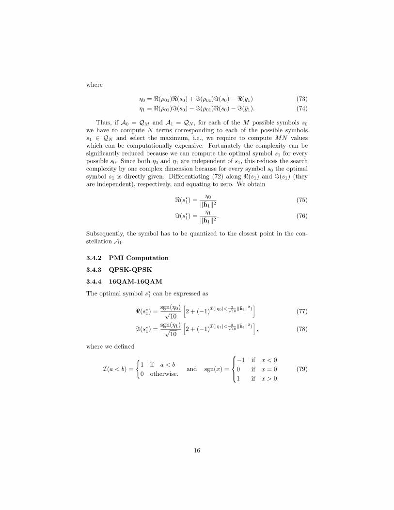
where
η0 = <(ρ01)<(s0) + =(ρ01)=(s0)−<(y1) (73)η1 = <(ρ01)=(s0)−=(ρ01)<(s0)−=(y1). (74)
Thus, if A0 = QM and A1 = QN , for each of the M possible symbols s0
we have to compute N terms corresponding to each of the possible symbolss1 ∈ QN and select the maximum, i.e., we require to compute MN valueswhich can be computationally expensive. Fortunately the complexity can besignificantly reduced because we can compute the optimal symbol s1 for everypossible s0. Since both η0 and η1 are independent of s1, this reduces the searchcomplexity by one complex dimension because for every symbol s0 the optimalsymbol s1 is directly given. Differentiating (72) along <(s1) and =(s1) (theyare independent), respectively, and equating to zero. We obtain
<(s?1) =η0
‖h1‖2(75)
=(s?1) =η1
‖h1‖2. (76)
Subsequently, the symbol has to be quantized to the closest point in the con-stellation A1.
3.4.2 PMI Computation
3.4.3 QPSK-QPSK
3.4.4 16QAM-16QAM
The optimal symbol s?1 can be expressed as
<(s?1) =sgn(η0)√
10
[2 + (−1)I(|η0|< 2√
10‖h1‖2)
](77)
=(s?1) =sgn(η1)√
10
[2 + (−1)I(|η1|< 2√
10‖h1‖2)
], (78)
where we defined
I(a < b) =
{1 if a < b
0 otherwise.and sgn(x) =
−1 if x < 00 if x = 01 if x > 0.
(79)
16
3.5 MU-MIMO
We distinguish two different kind of receivers: A simple one, that ignores theinterference of the other user and assumes it to be noise. The second one is aninterference-aware receiver and computes the LLRs assuming specific constel-lation for the interfering symbol. The interference-aware receiver is essentiallythe same as in the ML decoder in the SU-MIMO case, the sole differences are(i) we only decode the desired stream, (ii) we need a different pre-processing tocompute the effective channels and (iii) we have a different scaling due to theprecoding operation and the downlink power offset.
3.5.1 MU-MIMO nr × 2
Consider a system with nt = 2 transmit antennas and K = 2 users, where theUE of interest is endowed with nr receive antennas. Similar to SU-MIMO, thereceived signal reads
y = HGs + n = Hg0s0 + Hg1s1 + n (80)= h0s0 + h1s1 + n (81)
where H = [h0,h1, . . . ,hnr−1]H ∈ Cnr×2 is the channel from the transmitter touser 0, G = [g0, g1]2×2 is the concatenated precoding matrix and n ∈ Cnr isthe noise vector. Moreover, we defined the effective channels h0 , Hg0 andh1 , Hg1 of the desired symbol s0 and the interfering symbol s1, respectively.For the interference-aware receiver, the metric is identical to the SU-MIMO case(72) except that we do not require the sign of the interfering symbol s1 since(72) is maximized if <(s1) has the opposite sign of η0 and if =(s1) has theopposite sign of η1 and we obtain
λ = maxs0∈A1s1∈A2
{− ‖h0‖2|s0|2 − ‖h1‖2|s1|2 + 2[<(y0)<(s0) + =(y0)=(s0)]
+ 2|η0||<(s1)|+ 2|η1||=(s1)|}, (82)
where we defined the matched filter outputs y0 = hH0 y, y1 = hH
1 y and thecorrelation coefficient ρ01 , hH
0 h1.
3.5.2 PMI Computation
In the case of a single stream per user, the codebook G contains four precodingvectors g, i.e.,
G =1√2
{(11
),
(1−1
),
(1i
),
(1−i
)}. (83)
User k selects the precoding vector that maximizes his desired effective channelmagnitude ‖hk‖2 = ‖Hgk‖2, i.e.,
g?k = arg maxg∈G
{‖Hg‖2}. (84)
17
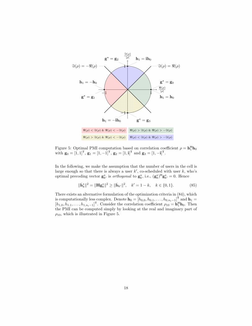
<(ρ)|ρ|
=(ρ)|ρ|
1−1
1
−1
h1 = ih0g? = g2
h1 = −ih0 g? = g3
h1 = h0
g? = g0h1 = −h0
g? = g1
=(ρ) = <(ρ)=(ρ) = −<(ρ)
<(ρ) > =(ρ) & <(ρ) > −=(ρ)<(ρ) < =(ρ) & <(ρ) < −=(ρ)
<(ρ) < =(ρ) & <(ρ) > −=(ρ)<(ρ) > =(ρ) & <(ρ) < −=(ρ)
Figure 5: Optimal PMI computation based on correlation coefficient ρ = hH1 h0
with g0 = [1, 1]T, g1 = [1,−1]T, g2 = [1, i]T and g3 = [1,−i]T.
In the following, we make the assumption that the number of users in the cell islarge enough so that there is always a user k′, co-scheduled with user k, who’soptimal precoding vector g?k′ is orthogonal to g?k, i.e., (g?k)Hg?k′ = 0. Hence
‖h?k‖2 = ‖Hg?k‖2 ≥ ‖hk′‖2, k′ = 1− k, k ∈ {0, 1}. (85)
There exists an alternative formulation of the optimization criteria in (84), whichis computationally less complex. Denote h0 = [h0,0, h0,1, . . . , h0,nr−1]T and h1 =[h1,0, h1,1, . . . , h1,nr−1]T. Consider the correlation coefficient ρ10 = hH
1 h0. Thenthe PMI can be computed simply by looking at the real and imaginary part ofρ10, which is illustrated in Figure 5.
18
3.6 Optimal Decoding
First we consider the case where M = N , i.e., the alphabets of both symbolsare identical. Moreover, we assume that the symbols have unit energy, i.e.,E[sks∗k] = 1.
3.6.1 QPSK-QPSK
Let us first consider equal energy alphabets and start with the simplest casewhere s0, s1 ∈ Q4. Since all amplitudes are identical we have from (82)
λ = maxs0∈Q4s1∈Q4
{<(y0)<(s0) + =(y0)=(s0) + |η0||<(s1)|+ |η1||=(s1)|} . (86)
The LLR for the first bit of symbol s0 is given by
Λ1(s0) = max<(s0)=−1√
2
=(s0)=±1√2
{=(y0)=(s0) + |η0||<(s1)|+ |η1||=(s1)|}
− max<(s0)= 1√
2
=(s0)=±1√2
{=(y0)=(s0) + |η0||<(s1)|+ |η1||=(s1)|} −√
2<(y0). (87)
For the second bit we obtain
Λ2(s0) = max=(s0)=−1√
2
<(s0)=±1√2
{<(y0)<(s0) + |η0||<(s1)|+ |η1||=(s1)|}
− max=(s0)= 1√
2
<(s0)=±1√2
{<(y0)<(s0) + |η0||<(s1)|+ |η1||=(s1)|} −√
2=(y0). (88)
Note that we omitted the common scaling factor 2 in the LLR computation.
19
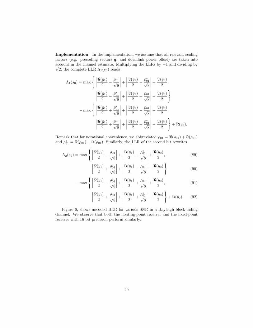
Implementation In the implementation, we assume that all relevant scalingfactors (e.g. precoding vectors gi and downlink power offset) are taken intoaccount in the channel estimate. Multiplying the LLRs by −1 and dividing by√
2, the complete LLR Λ1(s0) reads
Λ1(s0) = max
{∣∣∣∣<(y1)2− ρ01√
8
∣∣∣∣+∣∣∣∣=(y1)
2− ρ∗01√
8
∣∣∣∣+=(y0)
2,
∣∣∣∣<(y1)2− ρ∗01√
8
∣∣∣∣+∣∣∣∣=(y1)
2+ρ01√
8
∣∣∣∣− =(y0)2
}
−max
{∣∣∣∣<(y1)2
+ρ∗01√
8
∣∣∣∣+∣∣∣∣=(y1)
2− ρ01√
8
∣∣∣∣+=(y0)
2,
∣∣∣∣<(y1)2
+ρ01√
8
∣∣∣∣+∣∣∣∣=(y1)
2+ρ∗01√
8
∣∣∣∣− =(y0)2
}+ <(y0).
Remark that for notational convenience, we abbreviated ρ01 = <(ρ01) +=(ρ01)and ρ∗01 = <(ρ01)−=(ρ01). Similarly, the LLR of the second bit rewrites
Λ2(s0) = max
{∣∣∣∣<(y1)2− ρ01√
8
∣∣∣∣+∣∣∣∣=(y1)
2− ρ∗01√
8
∣∣∣∣+<(y0)
2, (89)
∣∣∣∣<(y1)2
+ρ∗01√
8
∣∣∣∣+∣∣∣∣=(y1)
2− ρ01√
8
∣∣∣∣− <(y0)2
}(90)
−max
{∣∣∣∣<(y1)2− ρ∗01√
8
∣∣∣∣+∣∣∣∣=(y1)
2+ρ01√
8
∣∣∣∣+<(y0)
2, (91)
∣∣∣∣<(y1)2
+ρ01√
8
∣∣∣∣+∣∣∣∣=(y1)
2+ρ∗01√
8
∣∣∣∣− <(y0)2
}+ =(y0). (92)
Figure 6, shows uncoded BER for various SNR in a Rayleigh block-fadingchannel. We observe that both the floating-point receiver and the fixed-pointreceiver with 16 bit precision perform similarly.
20
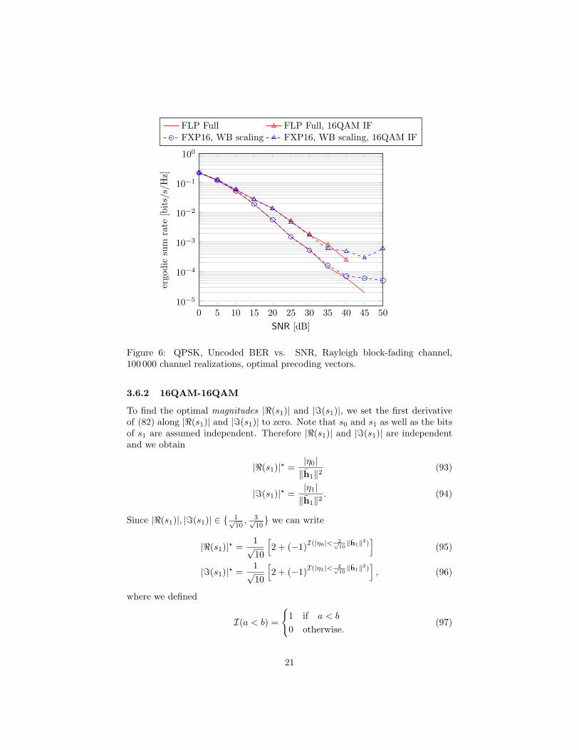
0 5 10 15 20 25 30 35 40 45 5010−5
10−4
10−3
10−2
10−1
100
SNR [dB]
ergo
dic
sum
rate
[bit
s/s/
Hz]
FLP Full FLP Full, 16QAM IFFXP16, WB scaling FXP16, WB scaling, 16QAM IF
Figure 6: QPSK, Uncoded BER vs. SNR, Rayleigh block-fading channel,100 000 channel realizations, optimal precoding vectors.
3.6.2 16QAM-16QAM
To find the optimal magnitudes |<(s1)| and |=(s1)|, we set the first derivativeof (82) along |<(s1)| and |=(s1)| to zero. Note that s0 and s1 as well as the bitsof s1 are assumed independent. Therefore |<(s1)| and |=(s1)| are independentand we obtain
|<(s1)|? =|η0|‖h1‖2
(93)
|=(s1)|? =|η1|‖h1‖2
. (94)
Since |<(s1)|, |=(s1)| ∈ { 1√10, 3√
10} we can write
|<(s1)|? =1√10
[2 + (−1)I(|η0|< 2√
10‖h1‖2)
](95)
|=(s1)|? =1√10
[2 + (−1)I(|η1|< 2√
10‖h1‖2)
], (96)
where we defined
I(a < b) =
{1 if a < b
0 otherwise.(97)
21
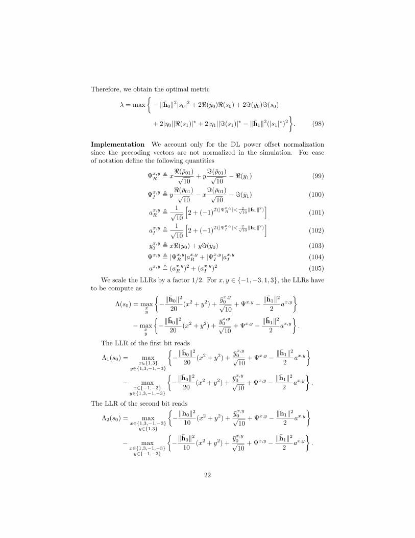
Therefore, we obtain the optimal metric
λ = max{− ‖h0‖2|s0|2 + 2<(y0)<(s0) + 2=(y0)=(s0)
+ 2|η0||<(s1)|? + 2|η1||=(s1)|? − ‖h1‖2(|s1|?)2
}. (98)
Implementation We account only for the DL power offset normalizationsince the precoding vectors are not normalized in the simulation. For easeof notation define the following quantities
Ψx,yR , x
<(ρ01)√10
+ y=(ρ01)√
10−<(y1) (99)
Ψx,yI , y
<(ρ01)√10− x=(ρ01)√
10−=(y1) (100)
ax,yR ,1√10
[2 + (−1)I(|Ψx,y
R |< 2√10‖h1‖2)
](101)
ax,yI ,1√10
[2 + (−1)I(|Ψx,y
I |< 2√10‖h1‖2)
](102)
yx,y0 , x<(y0) + y=(y0) (103)
Ψx,y , |Ψx,yR |a
x,yR + |Ψx,y
I |ax,yI (104)
ax,y , (ax,yR )2 + (ax,yI )2 (105)
We scale the LLRs by a factor 1/2. For x, y ∈ {−1,−3, 1, 3}, the LLRs haveto be compute as
Λ(s0) = maxxy
{−‖h0‖2
20(x2 + y2) +
yx,y0√10
+ Ψx,y − ‖h1‖2
2ax,y
}−max
xy
{−‖h0‖2
20(x2 + y2) +
yx,y0√10
+ Ψx,y − ‖h1‖2
2ax,y
}.
The LLR of the first bit reads
Λ1(s0) = maxx∈{1,3}
y∈{1,3,−1,−3}
{−‖h0‖2
20(x2 + y2) +
yx,y0√10
+ Ψx,y − ‖h1‖2
2ax,y
}
− maxx∈{−1,−3}
y∈{1,3,−1,−3}
{−‖h0‖2
20(x2 + y2) +
yx,y0√10
+ Ψx,y − ‖h1‖2
2ax,y
}.
The LLR of the second bit reads
Λ2(s0) = maxx∈{1,3,−1,−3}
y∈{1,3}
{−‖h0‖2
10(x2 + y2) +
yx,y0√10
+ Ψx,y − ‖h1‖2
2ax,y
}
− maxx∈{1,3,−1,−3}y∈{−1,−3}
{−‖h0‖2
10(x2 + y2) +
yx,y0√10
+ Ψx,y − ‖h1‖2
2ax,y
}.
22
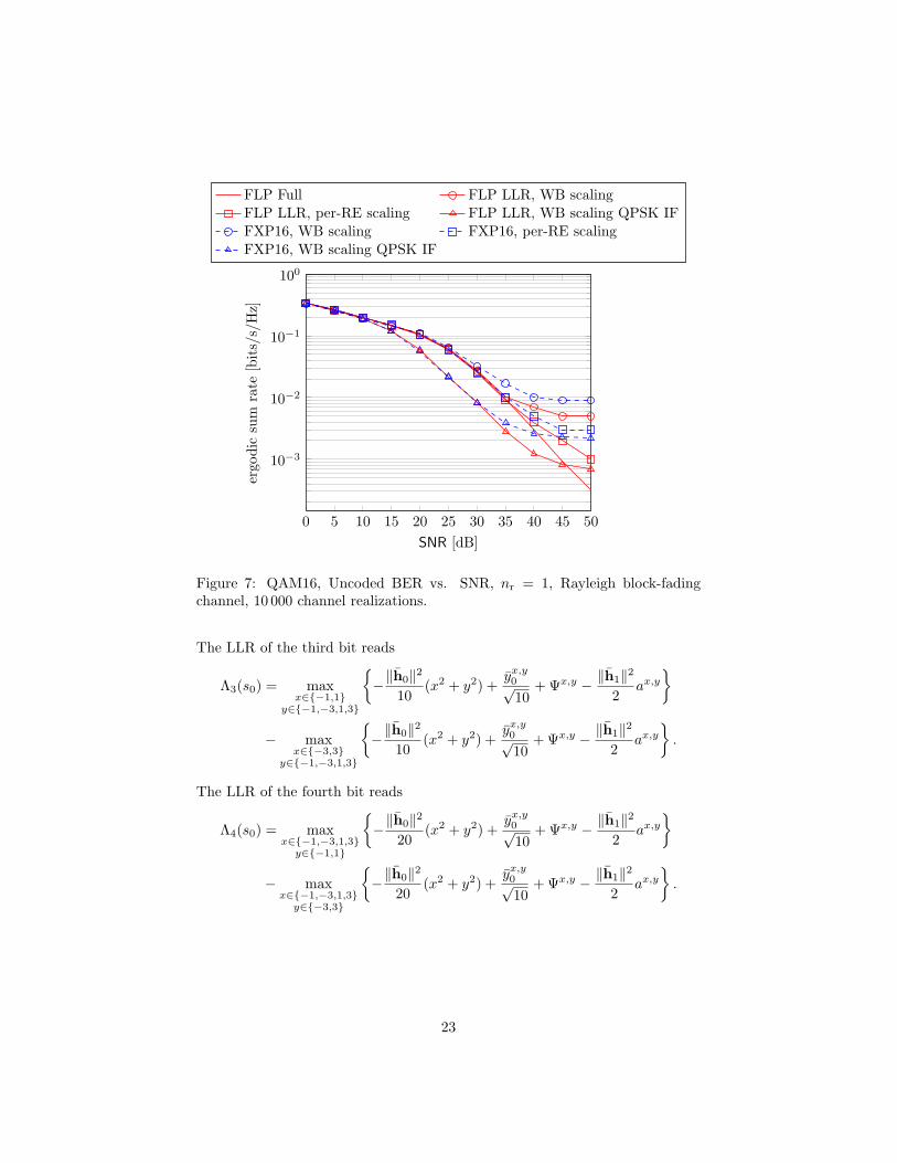
0 5 10 15 20 25 30 35 40 45 50
10−3
10−2
10−1
100
SNR [dB]
ergo
dic
sum
rate
[bit
s/s/
Hz]
FLP Full FLP LLR, WB scalingFLP LLR, per-RE scaling FLP LLR, WB scaling QPSK IFFXP16, WB scaling FXP16, per-RE scalingFXP16, WB scaling QPSK IF
Figure 7: QAM16, Uncoded BER vs. SNR, nr = 1, Rayleigh block-fadingchannel, 10 000 channel realizations.
The LLR of the third bit reads
Λ3(s0) = maxx∈{−1,1}
y∈{−1,−3,1,3}
{−‖h0‖2
10(x2 + y2) +
yx,y0√10
+ Ψx,y − ‖h1‖2
2ax,y
}
− maxx∈{−3,3}
y∈{−1,−3,1,3}
{−‖h0‖2
10(x2 + y2) +
yx,y0√10
+ Ψx,y − ‖h1‖2
2ax,y
}.
The LLR of the fourth bit reads
Λ4(s0) = maxx∈{−1,−3,1,3}y∈{−1,1}
{−‖h0‖2
20(x2 + y2) +
yx,y0√10
+ Ψx,y − ‖h1‖2
2ax,y
}
− maxx∈{−1,−3,1,3}y∈{−3,3}
{−‖h0‖2
20(x2 + y2) +
yx,y0√10
+ Ψx,y − ‖h1‖2
2ax,y
}.
23
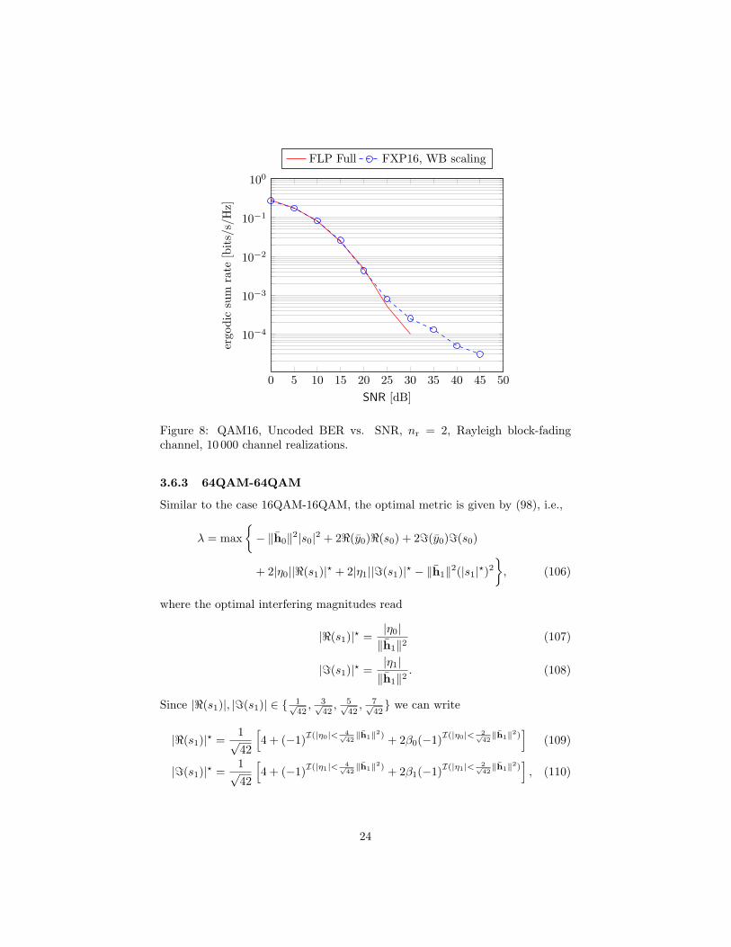
0 5 10 15 20 25 30 35 40 45 50
10−4
10−3
10−2
10−1
100
SNR [dB]
ergo
dic
sum
rate
[bit
s/s/
Hz]
FLP Full FXP16, WB scaling
Figure 8: QAM16, Uncoded BER vs. SNR, nr = 2, Rayleigh block-fadingchannel, 10 000 channel realizations.
3.6.3 64QAM-64QAM
Similar to the case 16QAM-16QAM, the optimal metric is given by (98), i.e.,
λ = max{− ‖h0‖2|s0|2 + 2<(y0)<(s0) + 2=(y0)=(s0)
+ 2|η0||<(s1)|? + 2|η1||=(s1)|? − ‖h1‖2(|s1|?)2
}, (106)
where the optimal interfering magnitudes read
|<(s1)|? =|η0|‖h1‖2
(107)
|=(s1)|? =|η1|‖h1‖2
. (108)
Since |<(s1)|, |=(s1)| ∈ { 1√42, 3√
42, 5√
42, 7√
42} we can write
|<(s1)|? =1√42
[4 + (−1)I(|η0|< 4√
42‖h1‖2) + 2β0(−1)I(|η0|< 2√
42‖h1‖2)
](109)
|=(s1)|? =1√42
[4 + (−1)I(|η1|< 4√
42‖h1‖2) + 2β1(−1)I(|η1|< 2√
42‖h1‖2)
], (110)
24
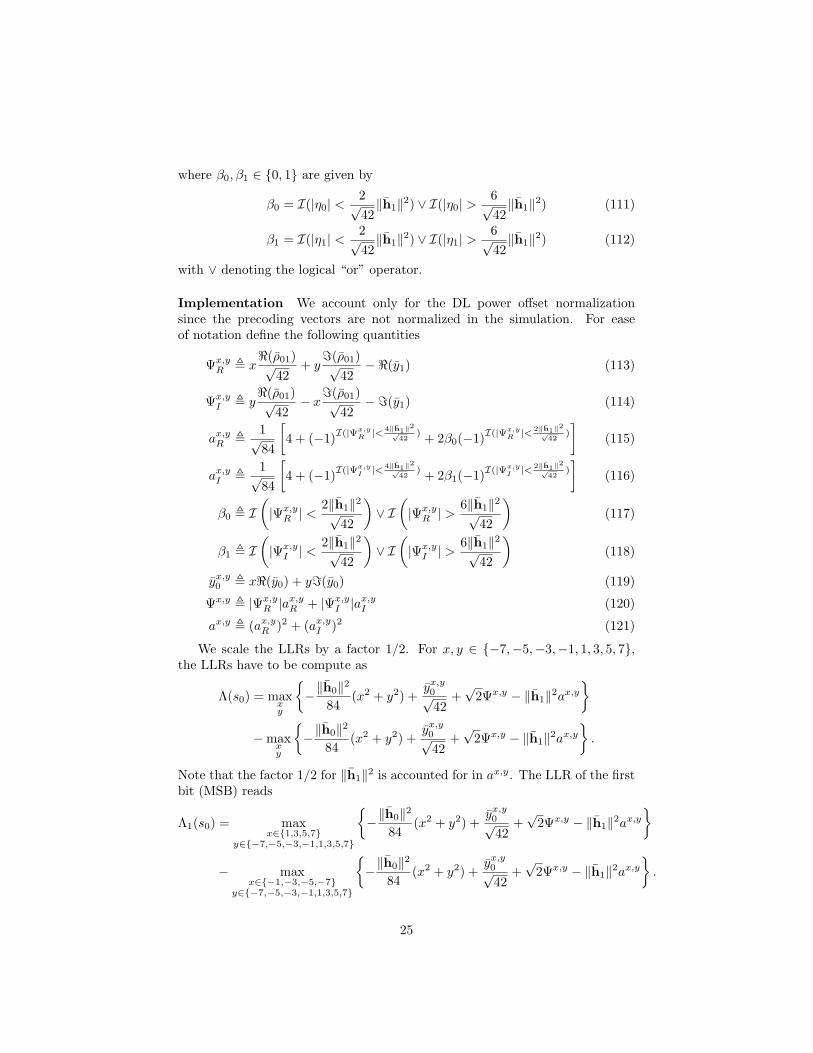
where β0, β1 ∈ {0, 1} are given by
β0 = I(|η0| <2√42‖h1‖2) ∨ I(|η0| >
6√42‖h1‖2) (111)
β1 = I(|η1| <2√42‖h1‖2) ∨ I(|η1| >
6√42‖h1‖2) (112)
with ∨ denoting the logical “or” operator.
Implementation We account only for the DL power offset normalizationsince the precoding vectors are not normalized in the simulation. For easeof notation define the following quantities
Ψx,yR , x
<(ρ01)√42
+ y=(ρ01)√
42−<(y1) (113)
Ψx,yI , y
<(ρ01)√42− x=(ρ01)√
42−=(y1) (114)
ax,yR ,1√84
[4 + (−1)I(|Ψx,y
R |< 4‖h1‖2
√42
) + 2β0(−1)I(|Ψx,yR |< 2‖h1‖
2√
42)
](115)
ax,yI ,1√84
[4 + (−1)I(|Ψx,y
I |< 4‖h1‖2
√42
) + 2β1(−1)I(|Ψx,yI |< 2‖h1‖
2√
42)
](116)
β0 , I(|Ψx,yR | <
2‖h1‖2√42
)∨ I
(|Ψx,yR | >
6‖h1‖2√42
)(117)
β1 , I(|Ψx,yI | <
2‖h1‖2√42
)∨ I
(|Ψx,yI | >
6‖h1‖2√42
)(118)
yx,y0 , x<(y0) + y=(y0) (119)
Ψx,y , |Ψx,yR |a
x,yR + |Ψx,y
I |ax,yI (120)
ax,y , (ax,yR )2 + (ax,yI )2 (121)
We scale the LLRs by a factor 1/2. For x, y ∈ {−7,−5,−3,−1, 1, 3, 5, 7},the LLRs have to be compute as
Λ(s0) = maxxy
{−‖h0‖2
84(x2 + y2) +
yx,y0√42
+√
2Ψx,y − ‖h1‖2ax,y}
−maxxy
{−‖h0‖2
84(x2 + y2) +
yx,y0√42
+√
2Ψx,y − ‖h1‖2ax,y}.
Note that the factor 1/2 for ‖h1‖2 is accounted for in ax,y. The LLR of the firstbit (MSB) reads
Λ1(s0) = maxx∈{1,3,5,7}
y∈{−7,−5,−3,−1,1,3,5,7}
{−‖h0‖2
84(x2 + y2) +
yx,y0√42
+√
2Ψx,y − ‖h1‖2ax,y}
− maxx∈{−1,−3,−5,−7}
y∈{−7,−5,−3,−1,1,3,5,7}
{−‖h0‖2
84(x2 + y2) +
yx,y0√42
+√
2Ψx,y − ‖h1‖2ax,y}.
25
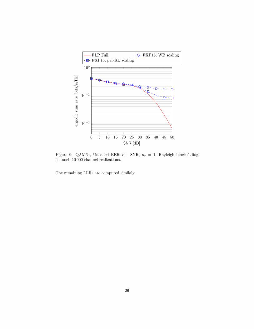
0 5 10 15 20 25 30 35 40 45 50
10−2
10−1
100
SNR [dB]
ergo
dic
sum
rate
[bit
s/s/
Hz]
FLP Full FXP16, WB scalingFXP16, per-RE scaling
Figure 9: QAM64, Uncoded BER vs. SNR, nr = 1, Rayleigh block-fadingchannel, 10 000 channel realizations.
The remaining LLRs are computed similaly.
26
0 5 10 15 20 25 30 35 40 45 50
10−4
10−3
10−2
10−1
100
SNR [dB]
ergo
dic
sum
rate
[bit
s/s/
Hz]
FLP Full FXP16, WB scaling
Figure 10: QAM64, Uncoded BER vs. SNR, nr = 2, Rayleigh block-fadingchannel, 10 000 channel realizations.
3.6.4 16QAM-QPSK
The maximizing metric reads
λ = maxs0∈Q16s0∈Q4
{− ‖h0‖2|s0|2 − ‖h1‖2|s0|2 + 2[<(y0)<(s0) + =(y0)=(s0)]
+ 2|η0||<(s0)|+ 2|η0||=(s0)|}. (122)
Since the interfering constellation has a constant amplitude the metric simplifiesto
λ = maxs0∈Q16s0∈Q4
{− ‖h0‖2|s0|2 + 2[<(y0)<(s0) + =(y0)=(s0)] +
√2P (|η0|+ |η0|)
}.
27

4 Future Work
This section summarizes various topics that need to be investigated.
4.1 4× 4 MIMO
A common setting in future practical mobile communication system will includea base-station endowed with nt = 4 transmit antennas. Thus optimal MIMOreceive algorithm in both SU and MU scenarios have to be studied.
4.2 SU-MIMO
The general system model is given in (67) and the distance metric D(y|Hs) =‖y −Hs‖2 takes the form
D(y|Hs) = ‖y − h0s0 − h1s1 − h2s2 − h3s3‖2
= ‖y‖2 + ‖h0‖2|s0|2 + ‖h1‖2|s1|2 + ‖h2‖2|s2|2 + ‖h3‖2|s3|2
− 2 [<(y0s∗0) + <(y1s
∗1) + <(y2s
∗2) + <(y3s
∗3)]
+ 2 [<(ρ01s∗0s1) + <(ρ02s
∗0s2) + <(ρ03s
∗0s3)]
+ 2 [<(ρ12s∗1s2) + <(ρ13s
∗1s3) + <(ρ23s
∗2s3)] ,
where yi = hHi y and ρij = hH
i hj . Omitting the common term ‖y‖2 and sepa-rating real and imaginary parts we obtain
λ = maxs0∈A0s1∈A1s2∈A2s3∈A3
{− ‖h0‖2|s0|2 − ‖h1‖2|s1|2 − ‖h2‖2|s2|2 − ‖h3‖2|s3|2
+ 2[<(y0)<(s0) + =(y0)=(s0)]
− 2[ηR01<(s1) + ηI01=(s1) + ηR02<(s2) + ηI02=(s2) + ηR03<(s3) + ηI03=(s3)]
− 2[νR12<(s2) + νI12=(s2) + νR13<(s3) + νI13=(s3) + νR23<(s3) + νI23=(s3)]}
where νRij and νIij are defined as
νRij = <(ρij)<(si) + =(ρij)=(si)
νIij = <(ρij)=(si)−=(ρij)<(si)
and ηR0i and ηI0i are given by
ηR0j = νR0j −<(yj) (123)
ηI0j = νI0j −=(yj). (124)
28
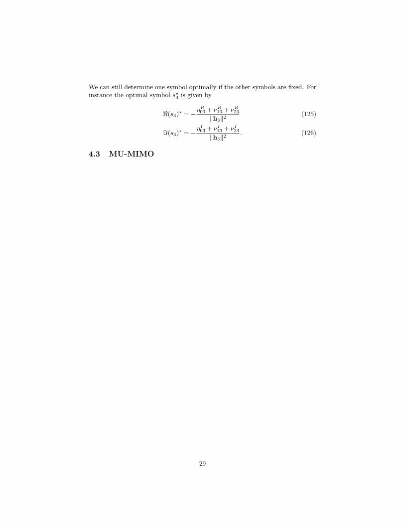
We can still determine one symbol optimally if the other symbols are fixed. Forinstance the optimal symbol s?3 is given by
<(s3)? = −ηR03 + νR13 + νR23
‖h3‖2(125)
=(s3)? = −ηI03 + νI13 + νI23
‖h3‖2. (126)
4.3 MU-MIMO
29
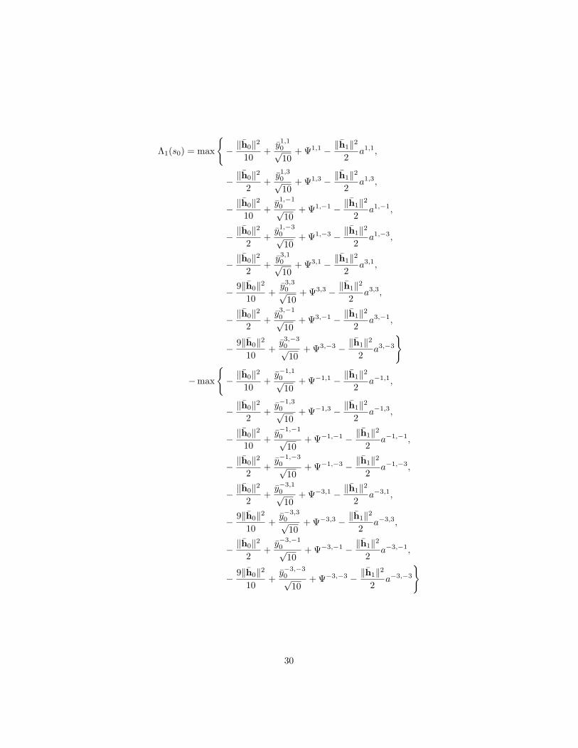
Λ1(s0) = max
{− ‖h0‖2
10+y1,1
0√10
+ Ψ1,1 − ‖h1‖2
2a1,1,
− ‖h0‖2
2+y1,3
0√10
+ Ψ1,3 − ‖h1‖2
2a1,3,
− ‖h0‖2
10+y1,−1
0√10
+ Ψ1,−1 − ‖h1‖2
2a1,−1,
− ‖h0‖2
2+y1,−3
0√10
+ Ψ1,−3 − ‖h1‖2
2a1,−3,
− ‖h0‖2
2+y3,1
0√10
+ Ψ3,1 − ‖h1‖2
2a3,1,
− 9‖h0‖2
10+y3,3
0√10
+ Ψ3,3 − ‖h1‖2
2a3,3,
− ‖h0‖2
2+y3,−1
0√10
+ Ψ3,−1 − ‖h1‖2
2a3,−1,
− 9‖h0‖2
10+y3,−3
0√10
+ Ψ3,−3 − ‖h1‖2
2a3,−3
}
−max
{− ‖h0‖2
10+y−1,1
0√10
+ Ψ−1,1 − ‖h1‖2
2a−1,1,
− ‖h0‖2
2+y−1,3
0√10
+ Ψ−1,3 − ‖h1‖2
2a−1,3,
− ‖h0‖2
10+y−1,−1
0√10
+ Ψ−1,−1 − ‖h1‖2
2a−1,−1,
− ‖h0‖2
2+y−1,−3
0√10
+ Ψ−1,−3 − ‖h1‖2
2a−1,−3,
− ‖h0‖2
2+y−3,1
0√10
+ Ψ−3,1 − ‖h1‖2
2a−3,1,
− 9‖h0‖2
10+y−3,3
0√10
+ Ψ−3,3 − ‖h1‖2
2a−3,3,
− ‖h0‖2
2+y−3,−1
0√10
+ Ψ−3,−1 − ‖h1‖2
2a−3,−1,
− 9‖h0‖2
10+y−3,−3
0√10
+ Ψ−3,−3 − ‖h1‖2
2a−3,−3
}
30
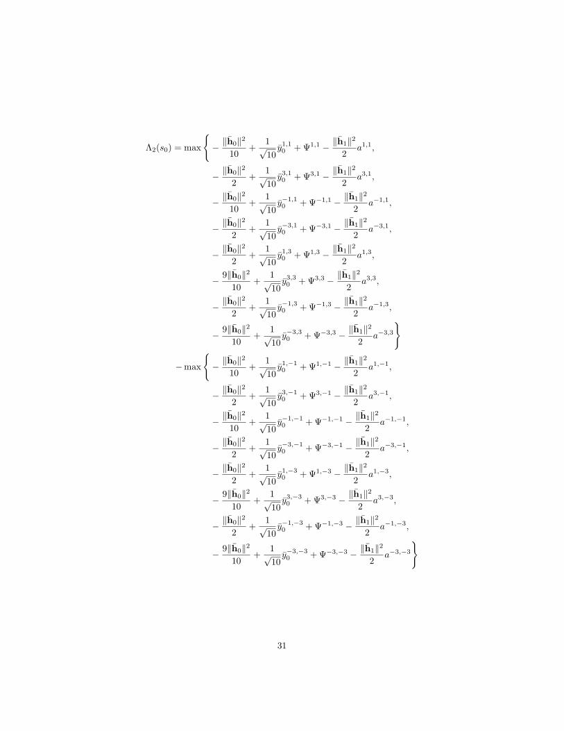
Λ2(s0) = max
{− ‖h0‖2
10+
1√10y1,1
0 + Ψ1,1 − ‖h1‖2
2a1,1,
− ‖h0‖2
2+
1√10y3,1
0 + Ψ3,1 − ‖h1‖2
2a3,1,
− ‖h0‖2
10+
1√10y−1,1
0 + Ψ−1,1 − ‖h1‖2
2a−1,1,
− ‖h0‖2
2+
1√10y−3,1
0 + Ψ−3,1 − ‖h1‖2
2a−3,1,
− ‖h0‖2
2+
1√10y1,3
0 + Ψ1,3 − ‖h1‖2
2a1,3,
− 9‖h0‖2
10+
1√10y3,3
0 + Ψ3,3 − ‖h1‖2
2a3,3,
− ‖h0‖2
2+
1√10y−1,3
0 + Ψ−1,3 − ‖h1‖2
2a−1,3,
− 9‖h0‖2
10+
1√10y−3,3
0 + Ψ−3,3 − ‖h1‖2
2a−3,3
}
−max
{− ‖h0‖2
10+
1√10y1,−1
0 + Ψ1,−1 − ‖h1‖2
2a1,−1,
− ‖h0‖2
2+
1√10y3,−1
0 + Ψ3,−1 − ‖h1‖2
2a3,−1,
− ‖h0‖2
10+
1√10y−1,−1
0 + Ψ−1,−1 − ‖h1‖2
2a−1,−1,
− ‖h0‖2
2+
1√10y−3,−1
0 + Ψ−3,−1 − ‖h1‖2
2a−3,−1,
− ‖h0‖2
2+
1√10y1,−3
0 + Ψ1,−3 − ‖h1‖2
2a1,−3,
− 9‖h0‖2
10+
1√10y3,−3
0 + Ψ3,−3 − ‖h1‖2
2a3,−3,
− ‖h0‖2
2+
1√10y−1,−3
0 + Ψ−1,−3 − ‖h1‖2
2a−1,−3,
− 9‖h0‖2
10+
1√10y−3,−3
0 + Ψ−3,−3 − ‖h1‖2
2a−3,−3
}
31