Embed Size (px)
Citation preview
Deliverable Title D2.4 - Material characterization for green chipless RFID report
Deliverable Lead: UNIPI
Related Work Package: WP2: Research and Definition of the requirements
Related Task: T2.4 Electromagnetic characterization of candidate materials
Author(s): Filippo Costa, Simone Genovesi, Christophe Mercier, David Girbau, Eduard Ibars
Participant(s): All Partners
Dissemination Level: Public
Due Submission Date: 01.09.2015
Actual Submission: 01.09.2015
Project Number 547761
Instrument: H2020-MSCA-RISE-2014
Start Date of Project: 01.01.2015
Duration: 36 months
Abstract
This document is Deliverable 2.4 related to WP2 – Research and Definition of the requirements. It reports the characterization of materials which will be used for designing chipless RFID sensors.
Project funded by the European Commission under the H2020 Programme – Marie Sklodoswska-Curie Action, Research and Innovation Staff Exchange.
D2.4 Material characterization for green chipless RFID report
EMERGENT 547761
Page 2 of 28
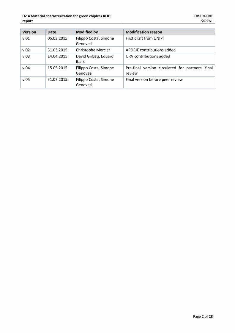
Version Date Modified by Modification reason
v.01 05.03.2015 Filippo Costa, Simone Genovesi
First draft from UNIPI
v.02 31.03.2015 Christophe Mercier ARDEJE contributions added
v.03 14.04.2015 David Girbau, Eduard Ibars
URV contributions added
v.04 15.05.2015 Filippo Costa, Simone Genovesi
Pre-final version circulated for partners’ final review
v.05
31.07.2015 Filippo Costa, Simone Genovesi
Final version before peer review
D2.4 Material characterization for green chipless RFID report
EMERGENT 547761
Page 3 of 28
Table of Contents
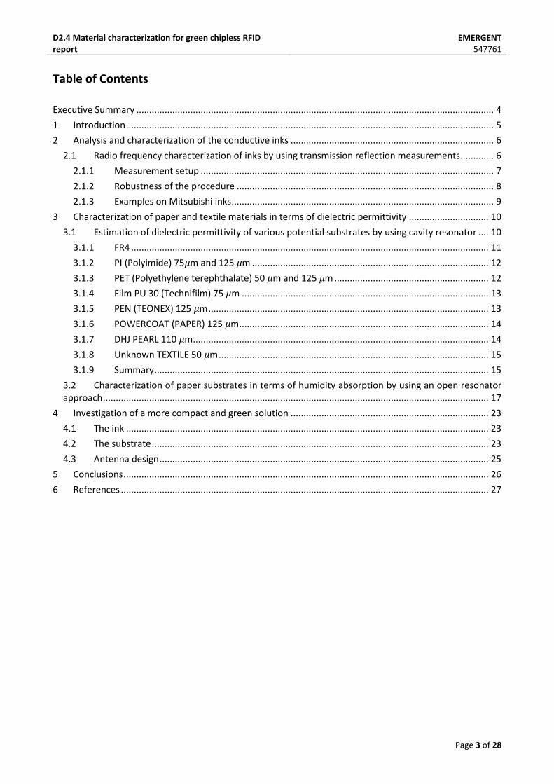
Executive Summary ........................................................................................................................................... 4
1 Introduction ............................................................................................................................................... 5
2 Analysis and characterization of the conductive inks ............................................................................... 6
2.1 Radio frequency characterization of inks by using transmission reflection measurements ............. 6
2.1.1 Measurement setup .................................................................................................................. 7
2.1.2 Robustness of the procedure .................................................................................................... 8
2.1.3 Examples on Mitsubishi inks ...................................................................................................... 9
3 Characterization of paper and textile materials in terms of dielectric permittivity ............................... 10
3.1 Estimation of dielectric permittivity of various potential substrates by using cavity resonator .... 10
3.1.1 FR4 ........................................................................................................................................... 11
3.1.2 PI (Polyimide) 75𝜇m and 125 𝜇m ............................................................................................ 12
3.1.3 PET (Polyethylene terephthalate) 50 𝜇m and 125 𝜇m ............................................................ 12
3.1.4 Film PU 30 (Technifilm) 75 𝜇m ................................................................................................ 13
3.1.5 PEN (TEONEX) 125 𝜇m ............................................................................................................. 13
3.1.6 POWERCOAT (PAPER) 125 𝜇m ................................................................................................. 14
3.1.7 DHJ PEARL 110 𝜇m ................................................................................................................... 14
3.1.8 Unknown TEXTILE 50 𝜇m ......................................................................................................... 15
3.1.9 Summary .................................................................................................................................. 15
3.2 Characterization of paper substrates in terms of humidity absorption by using an open resonator approach ...................................................................................................................................................... 17
4 Investigation of a more compact and green solution ............................................................................. 23
4.1 The ink ............................................................................................................................................. 23
4.2 The substrate ................................................................................................................................... 23
4.3 Antenna design ................................................................................................................................ 25
5 Conclusions .............................................................................................................................................. 26
6 References ............................................................................................................................................... 27
D2.4 Material characterization for green chipless RFID report
EMERGENT 547761
Page 4 of 28
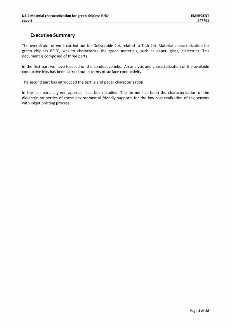
Executive Summary
The overall aim of work carried out for Deliverable 2.4, related to Task 2.4 ‘Material characterization for green chipless RFID’, was to characterize the green materials, such as paper, glass, dielectrics. This document is composed of three parts. In the first part we have focused on the conductive inks. An analysis and characterization of the available conductive inks has been carried out in terms of surface conductivity. The second part has introduced the textile and paper characterization. In the last part, a green approach has been studied. The former has been the characterization of the dielectric properties of these environmental friendly supports for the low-cost realization of tag sensors with inkjet printing process.
D2.4 Material characterization for green chipless RFID report
EMERGENT 547761
Page 5 of 28
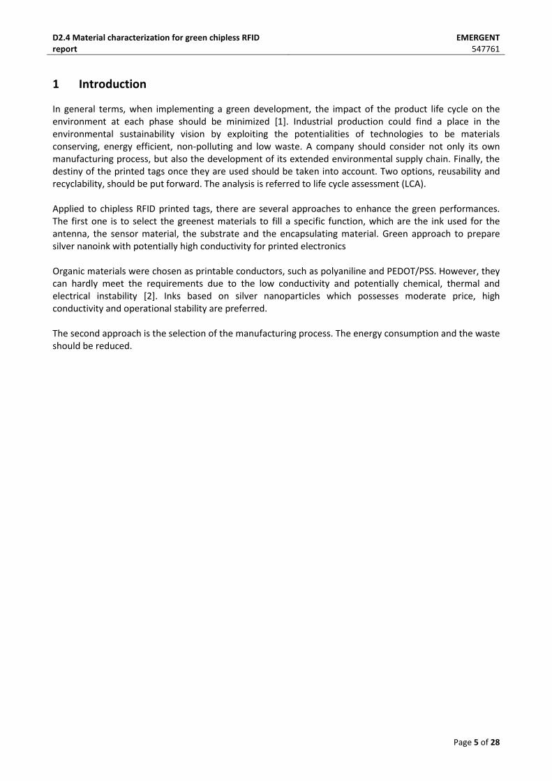
1 Introduction
In general terms, when implementing a green development, the impact of the product life cycle on the environment at each phase should be minimized [1]. Industrial production could find a place in the environmental sustainability vision by exploiting the potentialities of technologies to be materials conserving, energy efficient, non-polluting and low waste. A company should consider not only its own manufacturing process, but also the development of its extended environmental supply chain. Finally, the destiny of the printed tags once they are used should be taken into account. Two options, reusability and recyclability, should be put forward. The analysis is referred to life cycle assessment (LCA). Applied to chipless RFID printed tags, there are several approaches to enhance the green performances. The first one is to select the greenest materials to fill a specific function, which are the ink used for the antenna, the sensor material, the substrate and the encapsulating material. Green approach to prepare silver nanoink with potentially high conductivity for printed electronics Organic materials were chosen as printable conductors, such as polyaniline and PEDOT/PSS. However, they can hardly meet the requirements due to the low conductivity and potentially chemical, thermal and electrical instability [2]. Inks based on silver nanoparticles which possesses moderate price, high conductivity and operational stability are preferred. The second approach is the selection of the manufacturing process. The energy consumption and the waste should be reduced.
D2.4 Material characterization for green chipless RFID report
EMERGENT 547761
Page 6 of 28
2 Analysis and characterization of the conductive inks The most common technique to measure the DC surface resistance is Van Der Pauw method based on the four-point probes [2]. The measurement of the surface impedance at microwave frequencies can be accurately carried out through ad-hoc resonant cavities [3], [4] but the measurement requires an ad-hoc setup which may be expensive and narrowband. A wideband estimation of the surface impedance can be performed by recurring to a transmission/reflection measurement in free space or in a guided device [5]–[9]. Often the reflection coefficient is used for this kind of inverse problem [5], [10] but the use of transmission coefficient allows achieving more accurate results [7], [9]. The surface impedance of the resistive ink printed on a substrate can be derived indirectly through the calculation of the effective permittivity of the sample [7] if the substrate thickness is very small compared to the guided wavelength or directly by using a model which takes into account the presence of the substrate [9].
2.1 Radio frequency characterization of inks by using transmission reflection measurements
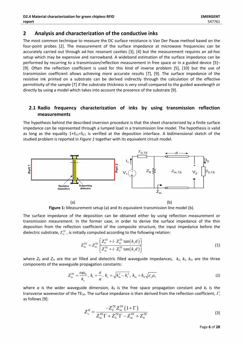
The hypothesis behind the described inversion procedure is that the sheet characterized by a finite surface impedance can be represented through a lumped load in a transmission line model. The hypothesis is valid as long as the equality 1+S11=S21 is verified at the deposition interface. A bidimensional sketch of the studied problem is reported in Figure 1 together with its equivalent circuit model.
(a) (b) Figure 1: Measurement setup (a) and its equivalent transmission line model (b).
The surface impedance of the deposition can be obtained either by using reflection measurement or transmission meaurement. In the former case, in order to derive the surface impedance of the thin deposition from the reflection coefficient of the composite structure, the input impedance before the
dielectric substrate, TE
inZ , is initially computed according to the following relation:
0
0
tan
tan
TE TE
m zTE TE
in m TE TE
m z
Z i Z k dZ Z
Z i Z k d
(1)
where Z0 and Zm are the air filled and dielectric filled waveguide impedances, kz, kt, km are the three components of the waveguide propagation constants:
2 200, , , TE
m t z m t m r r
z
Z k k k k k kk a
(2)
where a is the wider waveguide dimension, k0 is the free space propagation constant and kt is the
transverse wavevector of the TE10. The surface impedance is then derived from the reflection coefficient, , as follows [9]:
0
0 0
1TE TE
inR
s TE TE TE TE
in in
Z ZZ
Z Z Z Z
(3)
D2.4 Material characterization for green chipless RFID report
EMERGENT 547761
Page 7 of 28
The reflection coefficient of the analysed network coincides with the S11 since the load is represented by the free space impedance. If the dielectric substrate is thin compared to guided wavelength inside the dielectric substrate, the relation (3) simplifies to:
0 1
2
TE
R
s
ZZ
if d<<λ (4)
Defining V1 and V2 as the input and the output voltages of the system, the S21 of the structure
(21 2 12S V V ) is derived by solving the following matrix system:
0
0
21 1
21
TE
TE
VV I Z A B
V ZC DI
(5)
where the terms A,B,C,D are the elements of the transmission line matrix of the entire system which is defined as follows:
cos sin1 0
sin1/ 1 cos
m
m
TE
z z
zs zTE
k d jZ k dA B
k dZC D j k d
Z
(6)
Once solved the system the expression of the S21 is derived:
2 2 2
0 00
0
212
2
cos sinTE TE TE TETE
s ss m m
TE TEs s m
Z Z Z Z Z ZZ Z
z zZ Z Z Z
s
k d j k d
(7)
The explicit expression of the surface impedance can be obtained from the relation (7) [9]:
0 0
0 0
21
2 2
21 21
cos sin
2 cos 1 sin
m m
m m
TE TE TE TE
z zT
sTE TE TE TE
z z
S Z Z Z k d jZ k dZ
Z Z S k d j Z Z S k d
(8)
If the thickness of the dielectric substrate is negligible, the relation (8) simplifies to:
021
212 1
TE
T
s
S ZZ
S
if d<<λ (9)
which is analogue to the relations employed in[11].
2.1.1 Measurement setup
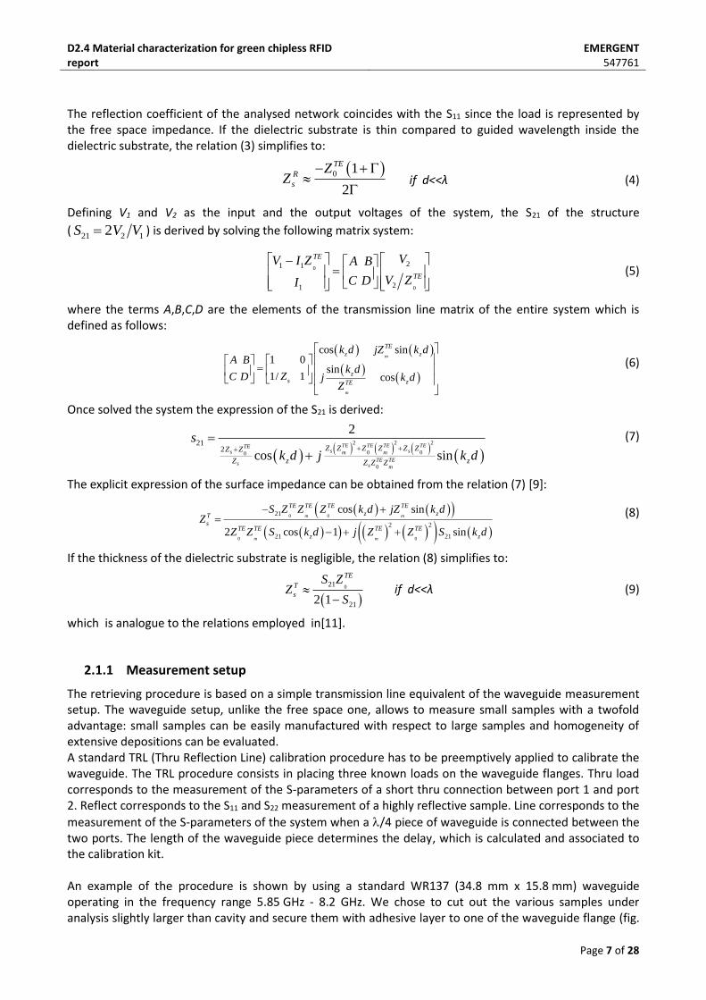
The retrieving procedure is based on a simple transmission line equivalent of the waveguide measurement setup. The waveguide setup, unlike the free space one, allows to measure small samples with a twofold advantage: small samples can be easily manufactured with respect to large samples and homogeneity of extensive depositions can be evaluated. A standard TRL (Thru Reflection Line) calibration procedure has to be preemptively applied to calibrate the waveguide. The TRL procedure consists in placing three known loads on the waveguide flanges. Thru load corresponds to the measurement of the S-parameters of a short thru connection between port 1 and port 2. Reflect corresponds to the S11 and S22 measurement of a highly reflective sample. Line corresponds to the
measurement of the S-parameters of the system when a /4 piece of waveguide is connected between the two ports. The length of the waveguide piece determines the delay, which is calculated and associated to the calibration kit. An example of the procedure is shown by using a standard WR137 (34.8 mm x 15.8 mm) waveguide operating in the frequency range 5.85 GHz - 8.2 GHz. We chose to cut out the various samples under analysis slightly larger than cavity and secure them with adhesive layer to one of the waveguide flange (fig.
D2.4 Material characterization for green chipless RFID report
EMERGENT 547761
Page 8 of 28
9). Although it should be guaranteed waveguide electrical continuity through sample excess, given its small thickness and its relative conductivity, we neglect this effect in the model. The latter configuration, even if it does not ensure the electric continuity of the waveguide across a short section of the waveguide, has a couple of advantages:
- it eliminates the strong capacitive behavior achieved with the previous setup and - it allows an accurate orthogonal positioning of the sample with respect to the waveguide [9].
(a) (b)
Figure 2: (a) Experimental setup and (b) sample positioning.
2.1.2 Robustness of the procedure
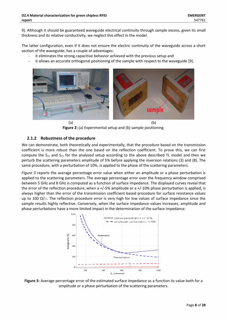
We can demonstrate, both theoretically and experimentally, that the procedure based on the transmission coefficient is more robust than the one based on the reflection coefficient. To prove this, we can first compute the S11 and S21 for the analysed setup according to the above described TL model and then we perturb the scattering parameters amplitude of 5% before applying the inversion relations (3) and (8). The same procedure, with a perturbation of 10%, is applied to the phase of the scattering parameters.
Figure 3 reports the average percentage error value when either an amplitude or a phase perturbation is applied to the scattering parameters. The average percentage error over the frequency window comprised between 5 GHz and 8 GHz is computed as a function of surface impedance. The displayed curves reveal that the error of the reflection procedure, when a +/-5% amplitude or a +/-10% phase perturbation is applied, is always higher than the error of the transmission coefficient based procedure for surface resistance values up to 100 Ω/. The reflection procedure error is very high for low values of surface impedance since the sample results highly reflective. Conversely, when the surface impedance values increases, amplitude and phase perturbations have a more limited impact in the determination of the surface impedance.
Figure 3: Average percentage error of the estimated surface impedance as a function its value both for a amplitude or a phase perturbation of the scattering parameters.
D2.4 Material characterization for green chipless RFID report
EMERGENT 547761
Page 9 of 28
2.1.3 Examples on Mitsubishi inks
To circumvent the need for time consuming and potentially damaging thermal sintering a new sintering method called chemical sintering was developed. It reduces barriers to using printable conductive inkjet in a research laboratory setting. Nonetheless, it maintains all the advantage associated with established inkjet circuit production. When silver nanoparticles smaller than 0.1 μm are dissolved in a solvent consisting of latex polymer and halide emulsion, conductivity appears several seconds after the solution is dried and to be smoothly released from an inkjet printer nozzle, the viscosity, surface tension, volatility, and particle size must be optimized.
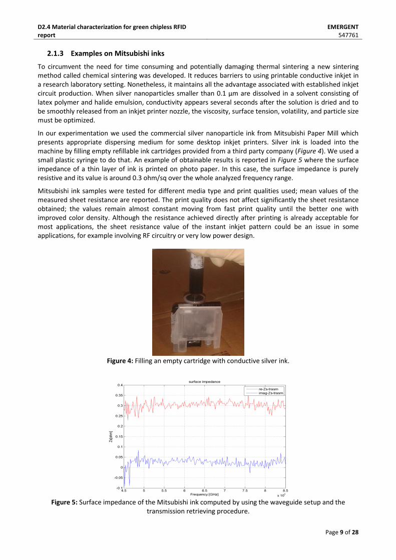
In our experimentation we used the commercial silver nanoparticle ink from Mitsubishi Paper Mill which presents appropriate dispersing medium for some desktop inkjet printers. Silver ink is loaded into the machine by filling empty refillable ink cartridges provided from a third party company (Figure 4). We used a small plastic syringe to do that. An example of obtainable results is reported in Figure 5 where the surface impedance of a thin layer of ink is printed on photo paper. In this case, the surface impedance is purely resistive and its value is around 0.3 ohm/sq over the whole analyzed frequency range.
Mitsubishi ink samples were tested for different media type and print qualities used; mean values of the measured sheet resistance are reported. The print quality does not affect significantly the sheet resistance obtained; the values remain almost constant moving from fast print quality until the better one with improved color density. Although the resistance achieved directly after printing is already acceptable for most applications, the sheet resistance value of the instant inkjet pattern could be an issue in some applications, for example involving RF circuitry or very low power design.
Figure 4: Filling an empty cartridge with conductive silver ink.
Figure 5: Surface impedance of the Mitsubishi ink computed by using the waveguide setup and the
transmission retrieving procedure.
D2.4 Material characterization for green chipless RFID report
EMERGENT 547761
Page 10 of 28
3 Characterization of paper and textile materials in terms of dielectric permittivity
The material complex permittivity is related to the ability of the material to interact with electromagnetic energy, whereas ε′ is the dielectric constant (real part), and ε′′ is the loss factor (imaginary part). ' ''
r rr j (10)
The dielectric constant ε′ also written determines how much of the incident energy is reflected at the air–sample interface and how much enters the sample relative to free space (ε′ = 1). The loss factor ε'' measures the degree to which an externally applied electric field will be converted to heat. The absorption of microwave by a dielectric material results in the microwaves giving up their energy to the material with a consequential rise in temperature. There is another important parameter called tanδ (tangent loss) and it measures the ability of the matrix to absorb microwave energy and dissipate heat to surrounding molecules, being responsible for the efficiency of microwave heating. It is calculated by the formula 11. ''
'tan r
r
(11)
These properties provide an indication of the electrical insulating ability of the material. For example, foods are in fact very poor insulators; therefore, they generally absorb a large fraction of the energy when placed in a microwave field resulting in instantaneous heating. The properties of complex permittivity will have a direct impact of characteristics of RFID tags. In the case of ε' (Relative permittivity), it is proportional to the wavelength for an electromagnetic wave. The dimensions of transmission lines and the dimensions of antennas are proportional to the wavelength for instance at same frequency higher relative permittivity will make smaller tags than tags with slower permittivity.
0
'
r
c
f
(12)
The efficiency of antennas UWB (Ultra Wide Band) and Narrowband used in RFID tags is directly related with the ε''(loss factor). A low loss factor will increase the efficiency of the antenna, for instance, higher values of gain will be reached and more reading distance can be obtained. In the case of FSS tags a high loss factor will induce an attenuation of resonations. In conclusion, at the same frequency for bigger permittivity’s, slower dimensions of the tag can be obtained and for lower losses more reading distance can be reached for UWB and Narrowband antennas in comparison of big losses. For instance high values of ε' and low values of ε'' are recommended.
3.1 Estimation of dielectric permittivity of various potential substrates by using cavity resonator
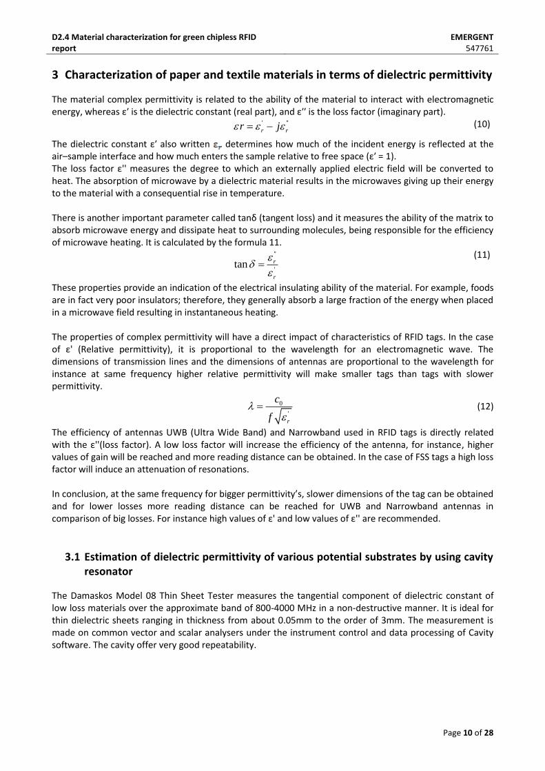
The Damaskos Model 08 Thin Sheet Tester measures the tangential component of dielectric constant of low loss materials over the approximate band of 800-4000 MHz in a non-destructive manner. It is ideal for thin dielectric sheets ranging in thickness from about 0.05mm to the order of 3mm. The measurement is made on common vector and scalar analysers under the instrument control and data processing of Cavity software. The cavity offer very good repeatability.
D2.4 Material characterization for green chipless RFID report
EMERGENT 547761
Page 11 of 28
Figure 6: Damaskos cavity and VNA The Thin Sheet Testers are expected to measure five or six resonances over its operating range. For some combination of thickness, dielectric constant, and loss tangent fewer or more resonances can be measured. Generally, lower values of thickness, dielectric constant, and loss tangent will allow more good resonances to be measured. The imaginary part of the dielectric constant and the loss tangent must not be less than zero: values less than zero may be caused by sample inhomogeneity, variations in sample thickness, or interferences by other cavity modes. Negative loss tangent values are most often seen with samples of low loss tangent materials and thin samples. The bad value should be discarded, and if possible, a sample with a thinner thickness measured to get a better value. This report will show the results of measuring the permittivity of some materials like PET (Polyethylene terephthalate), PI (Polyimide), Paper (Powercoat) and else, in Damaskos cavity. The procedure followed consists on taking three measures of each sample and then do an average of permittivity and loss tangent for each resonance then, this report will also cover the introduced error of the thickness and the precision of the measures comparing the Er with the datasheets of known materials.
3.1.1 FR4
FR-4 (or FR4) is a grade designation assigned to glass-reinforced epoxy laminate sheets, tubes, rods and printed circuit boards (PCB). FR-4 is a composite material composed of woven fiberglass cloth with an epoxy resin binder that is flame resistant (self-extinguishing).
Freq[GHz] 0,80 4,39 0,0372
1,26 4,38 0,0150
1,86 4,37 0,0156
2,51 4,35 0,0154
3,17 4,35 0,0154
3,84 4,34 0,0153
Freq[GHz] 1-10 3,9-4,3 0,02-0,025
Table 2: Measures of FR4 1.6mm substrate
Table 3: Typical values of FR4 in datasheets
The measures correspond with the common datasheets.
D2.4 Material characterization for green chipless RFID report
EMERGENT 547761
Page 12 of 28
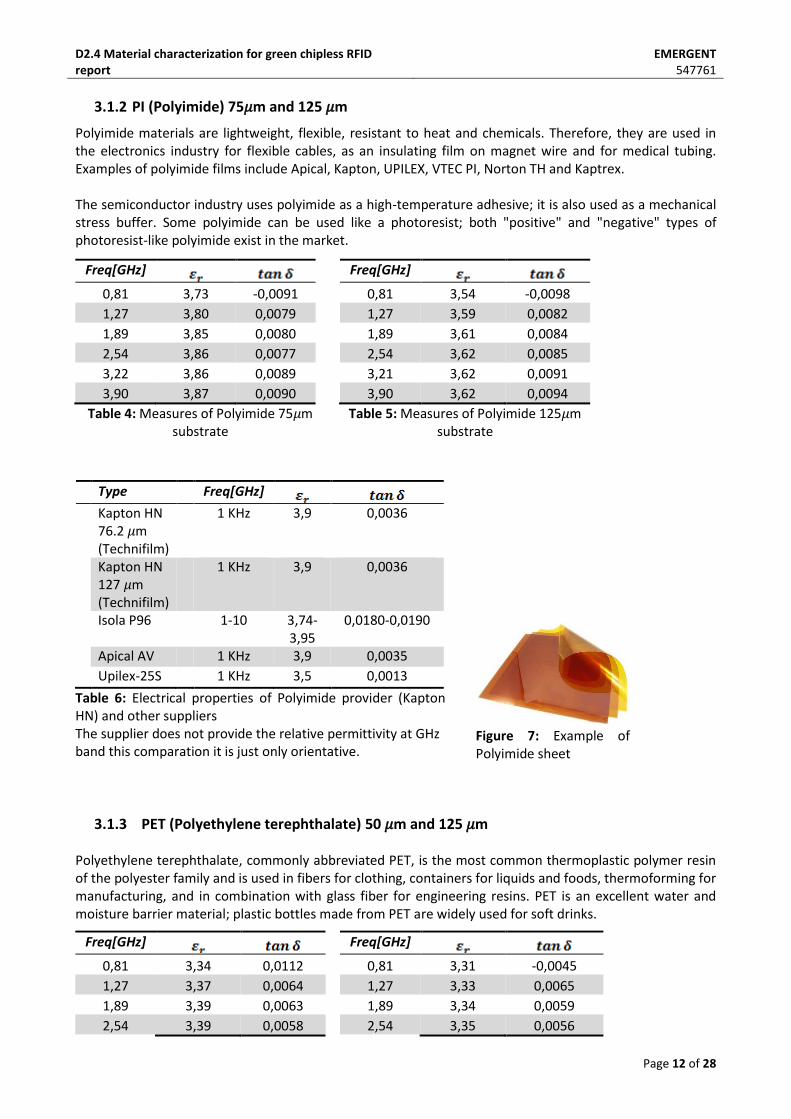
3.1.2 PI (Polyimide) 75𝜇m and 125 𝜇m
Polyimide materials are lightweight, flexible, resistant to heat and chemicals. Therefore, they are used in the electronics industry for flexible cables, as an insulating film on magnet wire and for medical tubing. Examples of polyimide films include Apical, Kapton, UPILEX, VTEC PI, Norton TH and Kaptrex. The semiconductor industry uses polyimide as a high-temperature adhesive; it is also used as a mechanical stress buffer. Some polyimide can be used like a photoresist; both "positive" and "negative" types of photoresist-like polyimide exist in the market.
Freq[GHz]
0,81 3,73 -0,0091
1,27 3,80 0,0079
1,89 3,85 0,0080
2,54 3,86 0,0077
3,22 3,86 0,0089
3,90 3,87 0,0090
Freq[GHz]
0,81 3,54 -0,0098
1,27 3,59 0,0082
1,89 3,61 0,0084
2,54 3,62 0,0085
3,21 3,62 0,0091
3,90 3,62 0,0094
Table 4: Measures of Polyimide 75𝜇m substrate
Table 5: Measures of Polyimide 125𝜇m substrate
Type Freq[GHz] Kapton HN
76.2 𝜇m (Technifilm)
1 KHz 3,9 0,0036
Kapton HN 127 𝜇m (Technifilm)
1 KHz 3,9 0,0036
Isola P96 1-10 3,74-3,95
0,0180-0,0190
Apical AV 1 KHz 3,9 0,0035
Upilex-25S 1 KHz 3,5 0,0013
Table 6: Electrical properties of Polyimide provider (Kapton HN) and other suppliers The supplier does not provide the relative permittivity at GHz band this comparation it is just only orientative.
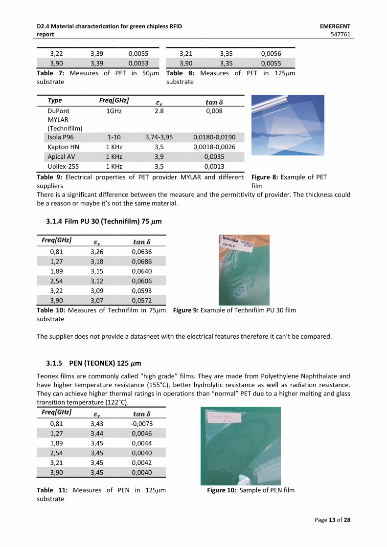
3.1.3 PET (Polyethylene terephthalate) 50 𝜇m and 125 𝜇m Polyethylene terephthalate, commonly abbreviated PET, is the most common thermoplastic polymer resin of the polyester family and is used in fibers for clothing, containers for liquids and foods, thermoforming for manufacturing, and in combination with glass fiber for engineering resins. PET is an excellent water and moisture barrier material; plastic bottles made from PET are widely used for soft drinks.
Freq[GHz]
0,81 3,34 0,0112
1,27 3,37 0,0064
1,89 3,39 0,0063
2,54 3,39 0,0058
Freq[GHz]
0,81 3,31 -0,0045
1,27 3,33 0,0065
1,89 3,34 0,0059
2,54 3,35 0,0056
Figure 7: Example of Polyimide sheet
D2.4 Material characterization for green chipless RFID report
EMERGENT 547761
Page 13 of 28
3,22 3,39 0,0055
3,90 3,39 0,0053
3,21 3,35 0,0056
3,90 3,35 0,0055
Table 7: Measures of PET in 50𝜇m substrate
Table 8: Measures of PET in 125𝜇m substrate
Type Freq[GHz] DuPont
MYLAR (Technifilm)
1GHz 2.8 0,008
Isola P96 1-10 3,74-3,95 0,0180-0,0190
Kapton HN 1 KHz 3,5 0,0018-0,0026
Apical AV 1 KHz 3,9 0,0035
Upilex-25S 1 KHz 3,5 0,0013
Table 9: Electrical properties of PET provider MYLAR and different suppliers
Figure 8: Example of PET film
There is a significant difference between the measure and the permittivity of provider. The thickness could be a reason or maybe it’s not the same material.
3.1.4 Film PU 30 (Technifilm) 75 𝜇m
Freq[GHz]
0,81 3,26 0,0636
1,27 3,18 0,0686
1,89 3,15 0,0640
2,54 3,12 0,0606
3,22 3,09 0,0593
3,90 3,07 0,0572
Table 10: Measures of Technifilm in 75𝜇m substrate
Figure 9: Example of Technifilm PU 30 film
The supplier does not provide a datasheet with the electrical features therefore it can’t be compared.
3.1.5 PEN (TEONEX) 125 𝜇m
Teonex films are commonly called “high grade” films. They are made from Polyethylene Naphthalate and have higher temperature resistance (155°C), better hydrolytic resistance as well as radiation resistance. They can achieve higher thermal ratings in operations than “normal” PET due to a higher melting and glass transition temperature (122°C).
Freq[GHz]
0,81 3,43 -0,0073
1,27 3,44 0,0046
1,89 3,45 0,0044
2,54 3,45 0,0040
3,21 3,45 0,0042
3,90 3,45 0,0040
Table 11: Measures of PEN in 125𝜇m substrate
Figure 10: Sample of PEN film
D2.4 Material characterization for green chipless RFID report
EMERGENT 547761
Page 14 of 28
Type Freq[GHz] TEONEX PEN Q51 25𝜇m
(Technifilm) 1 GHz 2,9 0,0050
Table 12: Electrical properties of PEN film provider TECHNIFILM in 25𝜇m There are some differences in permittivity due to the thickness of samples.
3.1.6 POWERCOAT (PAPER) 125 𝜇m
PowerCoat has been created in order to simplify the integration of electronic functions in graphic elements. This innovative paper offer a wide range of electronic possibilities whether it is inserted RFID label, a more sophisticated packaging, adds. PowerCoat paper has been made with cellulose fibers which gives him a good flexibility and a huge smooth. It is a really good paper for printing because it gives a lot of precision and a good ink adherence. It is the only paper that can resist to the high temperature required for the low resistance silver ink without bleaching. Finally, its impact on the environment is limited because it is biodegradable, recyclable and FSC certified.
Freq[GHz]
0,81 3,64 0,0608
1,27 3,53 0,1054
1,89 3,46 0,1000
2,54 3,41 0,0969
3,21 3,37 0,0931
3,90 3,34 0,0905
Table 13: Measures of Powercoat in 125𝜇m substrate
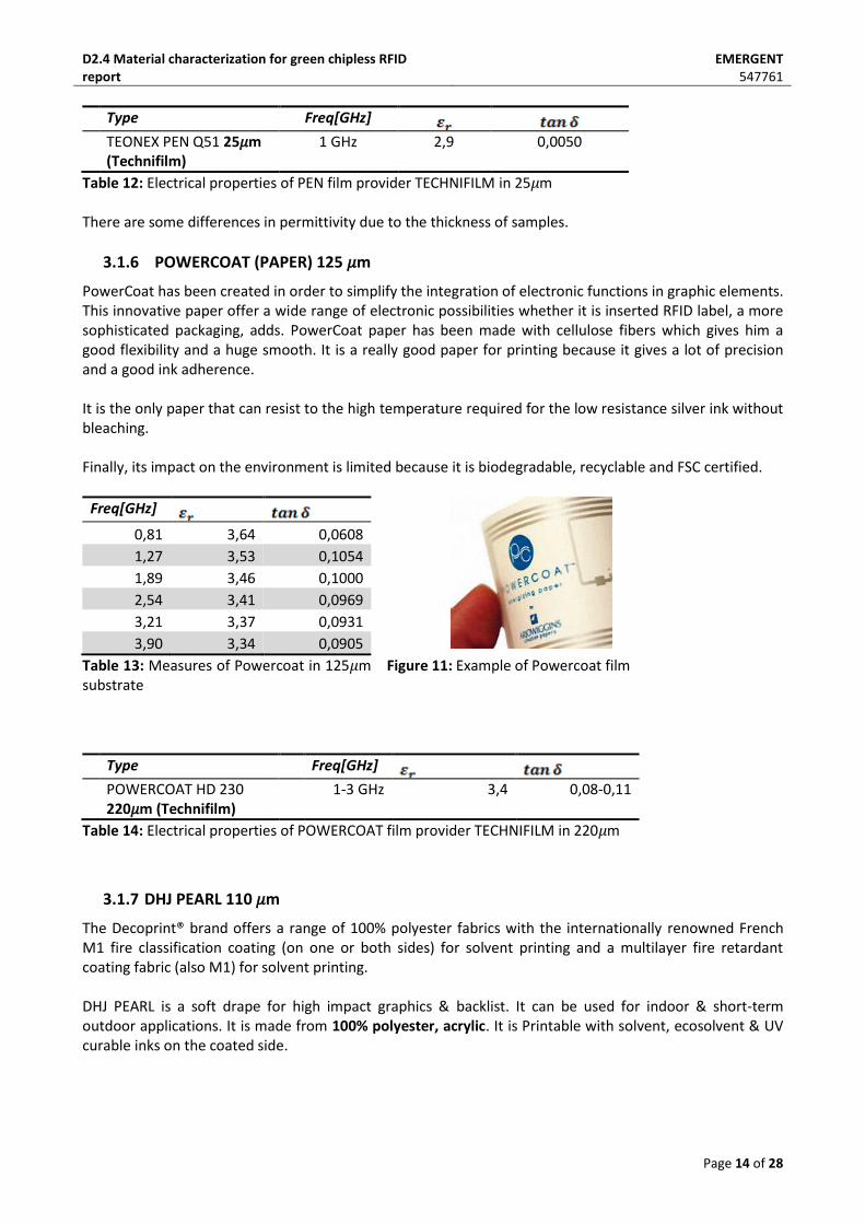
Figure 11: Example of Powercoat film
Type Freq[GHz] POWERCOAT HD 230
220𝜇m (Technifilm) 1-3 GHz 3,4 0,08-0,11
Table 14: Electrical properties of POWERCOAT film provider TECHNIFILM in 220𝜇m
3.1.7 DHJ PEARL 110 𝜇m
The Decoprint® brand offers a range of 100% polyester fabrics with the internationally renowned French M1 fire classification coating (on one or both sides) for solvent printing and a multilayer fire retardant coating fabric (also M1) for solvent printing. DHJ PEARL is a soft drape for high impact graphics & backlist. It can be used for indoor & short-term outdoor applications. It is made from 100% polyester, acrylic. It is Printable with solvent, ecosolvent & UV curable inks on the coated side.
D2.4 Material characterization for green chipless RFID report
EMERGENT 547761
Page 15 of 28
Freq[GHz]
0,81 2,88 -0,0079
1,27 2,88 0,0231
1,89 2,88 0,0215
2,54 2,88 0,0206
3,22 2,87 0,0199
3,90 2,87 0,0194
Table 15: Measures of DHJ pearl in 110𝜇m substrate
Figure 12: Example of DHJ pearl film
The supplier does not provide a datasheet with the electrical features, therefore it can’t be compared.
3.1.8 Unknown TEXTILE 50 𝜇m
Freq[GHz]
0,81 2,35 -0,0576
1,27 2,46 0,0045
1,89 2,50 0,0029
2,54 2,52 0,0033
3,22 2,52 0,0034
3,90 2,53 0,0033
Table 16: Measures of 50𝜇m substrate Figure 13: Example of sample film The supplier is not known, therefore it can’t be compared.
3.1.9 Summary
At the Table 17 it can be seen the typical values of permittivity of common RF commercial substrates.
Name tanδ Company
RO3003 3.00 0.0030 0.0010 Rogers RO3035 3.60 0.0054 0.0015 Rogers RO3006 6.50 0.0143 0.0022 Rogers RO3010 11.20 0.0246 0.0022 Rogers UltraLam 3850 3.14 0.0078 0.0025 Rogers RT/Duroid 5870 2.35 0.0028 0.0012 Rogers RT/Duroid 5880 2.20 0.0019 0.0009 Rogers CGK-500 5.0 0.0200 0.004 (8 GHz) Fluorocomposite CQF-500 2.3 0.0115 0.005 (12 GHz) Fluorocomposite CGC-500 10.0 0.0400 0.004 (6 GHz) Flourocomposite MHST 3.0 0.0069 0.0023 METCLAD Cuflon 2.1 0.0009 0.0004 (18 GHz) Polyfon TLC-32 3.20 0.0057 0.0018 (1.9 GHz) Taconic FR4 4.3 0.0860 0.0200
Table 17: Characteristics of commercial microwave substrates
D2.4 Material characterization for green chipless RFID report
EMERGENT 547761
Page 16 of 28
The Table 17 shows the values of loss factor from commercial RF (Radio Frequency) substrates; it can be
extracted than (loss factor) less than is enough for RF circuits. Higher values than are not recommendable for RF designs. The Table 18 shows the measured materials ordered from low loss factor to higher ones. Following the previous criterion, the conclusion is that the best materials are Textile, PEN, PET, PI, FR4 and DHJ pearl. The last two are in the limit for RF capabilities.
Name Tanδ (2.54GHz) Type
Textile 50u 2.52 0.008316 0.0033 Textile PEN 125u 3.45 0.0138 0.0040 Plastic PET 125u 3.35 0.01876 0.0056 Plastic PET 50u 3.39 0.028815 0.0085 Plastic PI 75u 3.86 0.029722 0.0077 Plastic PI 125u 3.62 0.03077 0.0085 Plastic FR4 4.35 0.06699 0.0154 Fiber glass DHJ Pearl 110u 2.88 0.059328 0.0206 Textile PU 30 3.12 0.189072 0.0606 Plastic PWR Coat 3.41 0.330429 0.0969 PAPER
Table 18: Measured properties of tested materials The thickness of substrate affects directly to the wavelength therefore the dimensions of the tag, in case of this report the thickness of all the samples are between 50 𝜇m and 125 𝜇m, at this scale this parameter is not critical, because the differences between them are very small.
It is also important to comment other material properties because they can play a major role in the design of RFID tags. Mechanical flexibility, the roughness, moisture absorption, light transparency, are important values to be considered and that are shown in Table 19.
Name PEN PET PI PowerCoat DHJ Pearl
Moisture Absorption
0.3% < 0.8% 4% 4-5% -
UV Transmission
92% 0-82% - 0% 0%
Roughness 13nm 38nm - 10nm - Total Light Transmission (TLT)
82% 83-86% 71-95% 5% 10%
Flexibility Very flexible Very flexible
Very flexible Flexible Very flexible
Biodegradable No No No Yes No Recyclable Yes Yes Yes Yes Yes Type Polymer Polymer Polymer Paper Textile
(polyester)
Table 19: Mechanical properties of tested materials A few conclusions can be extracted from Table 19. The first one consist on capabilities of humidity sensors, it can be seen that moisture absorption of PEN, PET PI and PowerCoat is equal or below than 5%, therefore these materials by themselves don’t have a good response in front of humidity. Consequently, it is recommendable to include another layer at the top of material based on materials that have a good response in front of humidity. Then the effective permittivity will change with the humidity and variations could be detected.
D2.4 Material characterization for green chipless RFID report
EMERGENT 547761
Page 17 of 28
The surface roughness has an impact in electromagnetic fields that is translated in losses if roughness is high. In case of substrates measured in this report, small values of roughness can be observed and this effect can be neglected. Other mechanical properties are also important for finding the correct application field, for example for meat packaging is important that material accomplish flexibility, transparency, biodegradability and the ability to be recycled.
3.2 Characterization of paper substrates in terms of humidity absorption by using an open resonator approach
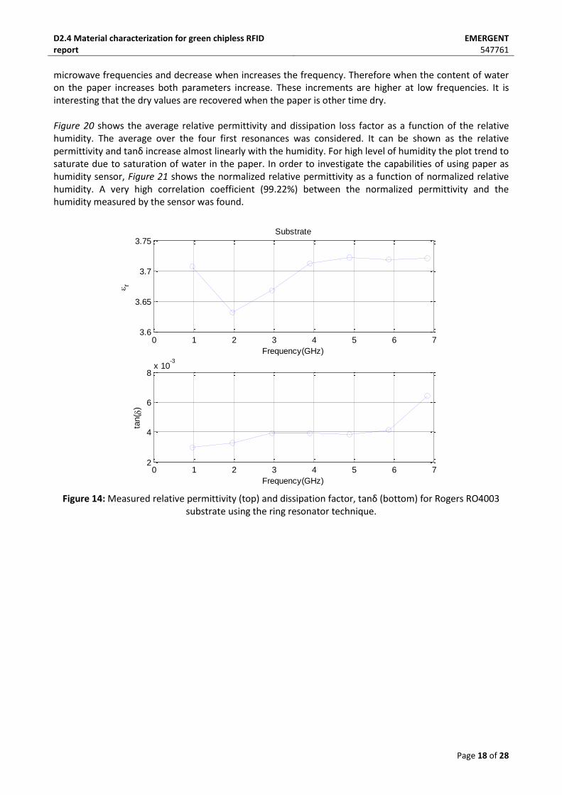
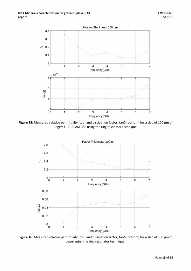
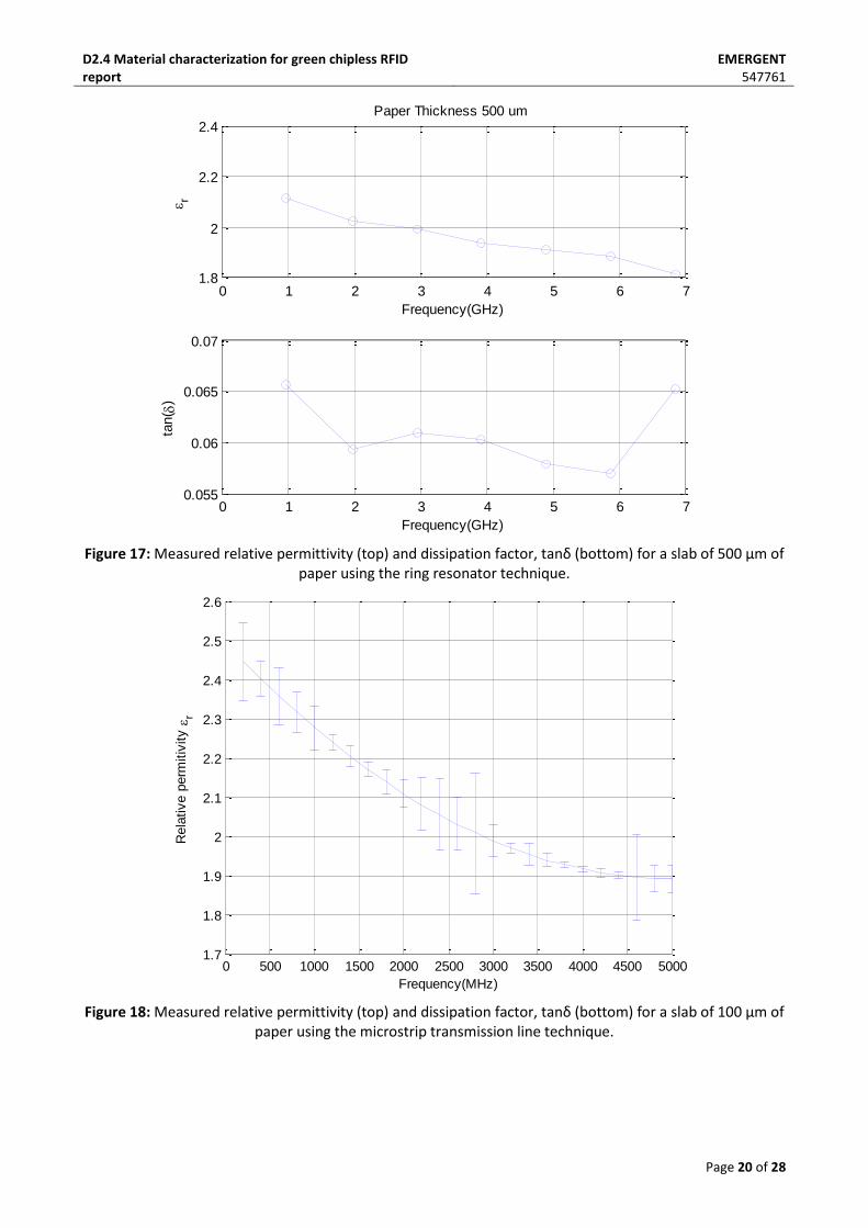
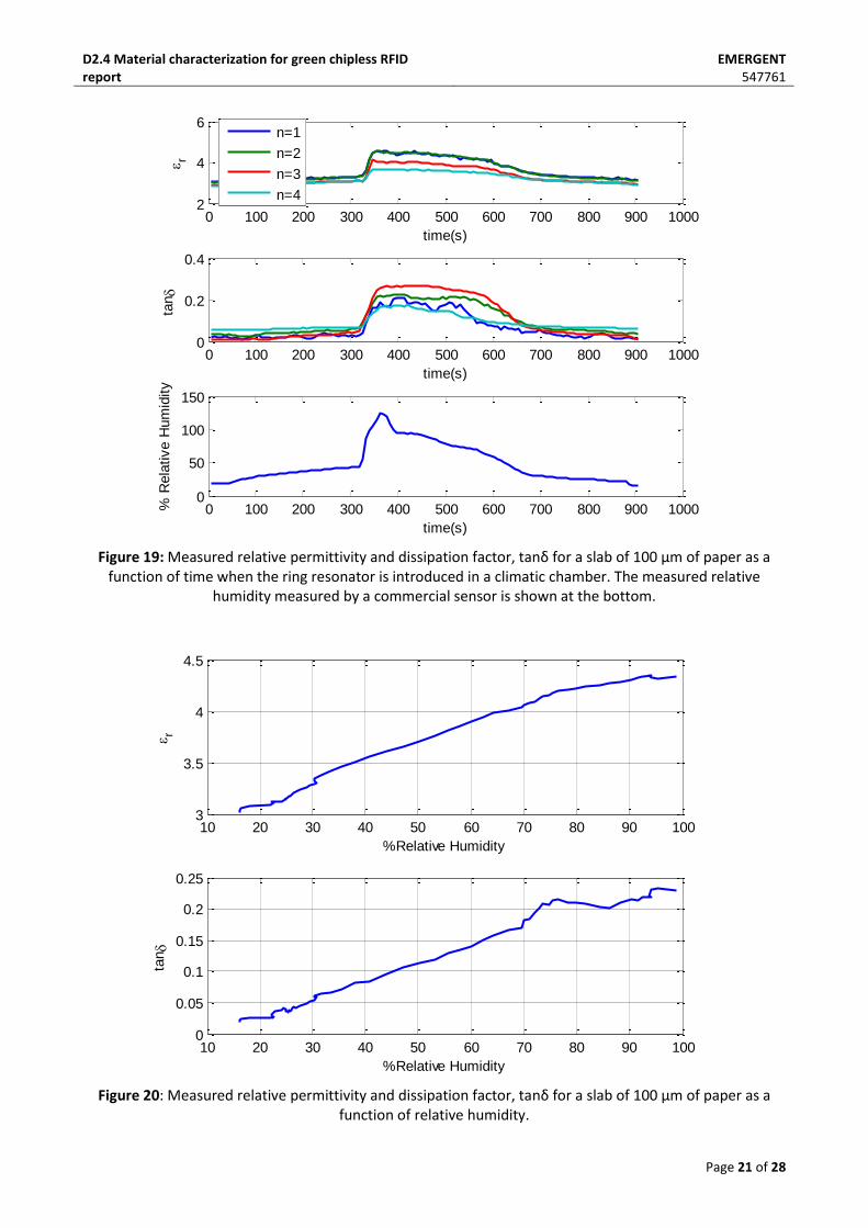
In this section some preliminary results using the ring resonator techniques will be described. In order to verify the method a ring resonator on Rogers RO4003 has been measured (h=32 mil, t=34 µm, W=1.81 mm, r=28.32 mm). The first resonant of the resonator is close to 1 GHz. Results of extracted relative permittivity and loss tangent is shown in Figure 14 for the first seven resonances. The measured values given by the manufacture using clamped stripline technique IPC-TM-650 2.5.5.5 are 3.38 and 0.0027, respectively at 10 GHz. However, the datasheet [12] says that clamped stripline method can potentially lower the actual dielectric constant due to presence of airgap. Dielectric constant in practice may be higher than the values listed. Therefore, the manufacture recommends to use the value of 3.55 at 10 GHz. Measured values given in the datasheet close to 3.65 are given in the datasheet between 1 GHz and 10 GHz. The measured values obtained fit within these margins. [13], [14] In order to test the modified ring resonator method, the resonator is measured with a slab of Roger ULTRALAM 3850 (Liquid Crystalline Polymer). Results of extracted relative permittivity and loss tangent are shown in Figure 15. The results for relative permittivity match well with the 3.14 value reported at 10 GHz given in the datasheet. However, the loss tangent obtained (around 0.004) is higher than reported by the manufactured. (0.0025 at 10 GHz). Figure 16 and Figure 17 shown measured results of a slab of paper (80gr paper photocopy) with thickness of 100 µm and 500 µm, respectively. Values around 2.4 and 0.06 are obtained for the relative permittivity and dissipation factor, respectively. These values match with reported values however depend on the several factors and impregnated materials. Therefore, an alternative method based on transmission line measurements is used as comparison [15]. This method allows obtaining the effective permittivity of a transmission line from calibrated S parameters. A modified technique is implemented where a slab of material is superimposed over the transmission. From the shift in the effective permittivity and using Momentum lookup table is possible to obtain the permittivity of the slab material. Figure 18 shows the results for the relative permittivity obtained. These results matches well with the permittivity obtained with ring resonator method especially when samples with higher thickness are used. However, with this technique has not been possible to obtain with accuracy the dissipation loss factor of thin samples. In addition, this method requires a custom microstrip calkit that it is not easy to implement due to the repeatability of PCB connectors and quality of the calkit standards. In the framework of the project, the ring resonator method proposed can be useful to investigate the sensitivity of material under test to physical or chemical parameters. For example, Figure 19 shows the variation of the relative permittivity and dissipation loss factor as function of the humidity for the four first resonances (fundamental resonance is close 1 GHz). The ring resonator with the slab of the material under test (paper of 100 µm thickness) was introduced in a custom climatic chamber where a flow of wet air was injected. A commercial humidity sensor was used to measure the relative humidity. When the humidity reaches the 100% and the ambient water starts to condensate, then a dry air is entered to decrease the relative humidity. This figure shows as paper absorbs water when increases the humidity changing its electrical parameters. The relative permittivity and dissipation loss factor of water is very high at
D2.4 Material characterization for green chipless RFID report
EMERGENT 547761
Page 18 of 28
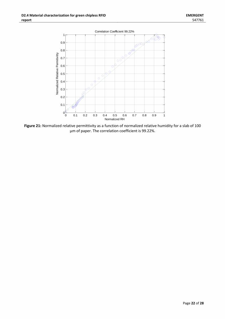
microwave frequencies and decrease when increases the frequency. Therefore when the content of water on the paper increases both parameters increase. These increments are higher at low frequencies. It is interesting that the dry values are recovered when the paper is other time dry. Figure 20 shows the average relative permittivity and dissipation loss factor as a function of the relative humidity. The average over the four first resonances was considered. It can be shown as the relative permittivity and tanδ increase almost linearly with the humidity. For high level of humidity the plot trend to saturate due to saturation of water in the paper. In order to investigate the capabilities of using paper as humidity sensor, Figure 21 shows the normalized relative permittivity as a function of normalized relative humidity. A very high correlation coefficient (99.22%) between the normalized permittivity and the humidity measured by the sensor was found.
0 1 2 3 4 5 6 73.6
3.65
3.7
3.75
Frequency(GHz)
r
Substrate
0 1 2 3 4 5 6 72
4
6
8x 10
-3
Frequency(GHz)
tan(
)
Figure 14: Measured relative permittivity (top) and dissipation factor, tanδ (bottom) for Rogers RO4003
substrate using the ring resonator technique.
D2.4 Material characterization for green chipless RFID report
EMERGENT 547761
Page 19 of 28
0 1 2 3 4 5 6 73
3.1
3.2
3.3
3.4
Frequency(GHz)
r
Ultralam Thickness 100 um
0 1 2 3 4 5 6 72
4
6
8x 10
-3
Frequency(GHz)
tan(
)
Figure 15: Measured relative permittivity (top) and dissipation factor, tanδ (bottom) for a slab of 100 µm of
Rogers ULTRALAM 380 using the ring resonator technique.
0 1 2 3 4 5 6 72
2.2
2.4
2.6
2.8
Frequency(GHz)
r
Paper Thickness 100 um
0 1 2 3 4 5 6 70
0.02
0.04
0.06
0.08
Frequency(GHz)
tan(
)
Figure 16: Measured relative permittivity (top) and dissipation factor, tanδ (bottom) for a slab of 100 µm of
paper using the ring resonator technique.
D2.4 Material characterization for green chipless RFID report
EMERGENT 547761
Page 20 of 28
0 1 2 3 4 5 6 71.8
2
2.2
2.4
Frequency(GHz)
r
Paper Thickness 500 um
0 1 2 3 4 5 6 70.055
0.06
0.065
0.07
Frequency(GHz)
tan(
)
Figure 17: Measured relative permittivity (top) and dissipation factor, tanδ (bottom) for a slab of 500 µm of
paper using the ring resonator technique.
0 500 1000 1500 2000 2500 3000 3500 4000 4500 50001.7
1.8
1.9
2
2.1
2.2
2.3
2.4
2.5
2.6
Frequency(MHz)
Rela
tive p
erm
itiv
ity
r
Figure 18: Measured relative permittivity (top) and dissipation factor, tanδ (bottom) for a slab of 100 µm of
paper using the microstrip transmission line technique.
D2.4 Material characterization for green chipless RFID report
EMERGENT 547761
Page 21 of 28
0 100 200 300 400 500 600 700 800 900 10002
4
6
time(s)
r
n=1
n=2
n=3
n=4
0 100 200 300 400 500 600 700 800 900 10000
0.2
0.4
time(s)
tan
0 100 200 300 400 500 600 700 800 900 10000
50
100
150
time(s)
% R
ela
tive H
um
idity
Figure 19: Measured relative permittivity and dissipation factor, tanδ for a slab of 100 µm of paper as a
function of time when the ring resonator is introduced in a climatic chamber. The measured relative humidity measured by a commercial sensor is shown at the bottom.
10 20 30 40 50 60 70 80 90 1003
3.5
4
4.5
%Relative Humidity
r
10 20 30 40 50 60 70 80 90 1000
0.05
0.1
0.15
0.2
0.25
%Relative Humidity
tan
Figure 20: Measured relative permittivity and dissipation factor, tanδ for a slab of 100 µm of paper as a
function of relative humidity.
D2.4 Material characterization for green chipless RFID report
EMERGENT 547761
Page 22 of 28
0 0.1 0.2 0.3 0.4 0.5 0.6 0.7 0.8 0.9 10
0.1
0.2
0.3
0.4
0.5
0.6
0.7
0.8
0.9
1
Norm
aliz
ed R
ela
tive P
erm
itiv
itty
Normalized RH
Correlation Coefficient 99.22%
Figure 21: Normalized relative permittivity as a function of normalized relative humidity for a slab of 100
µm of paper. The correlation coefficient is 99.22%.
D2.4 Material characterization for green chipless RFID report
EMERGENT 547761
Page 23 of 28
4 Investigation of a more compact and green solution Packaging is one of the possible applications. There are several approaches to promote the green aspect:
The ink
The substrate
The encapsulating material: a polymer film or preferable varnish could be used.
The manufacturing process: energy, waste
The antenna design
Some of the abovementioned aspects are analysed in more detail below.
4.1 The ink
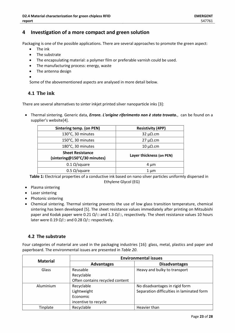
There are several alternatives to sinter inkjet printed silver nanoparticle inks [3]:
Thermal sintering. Generic data, Errore. L'origine riferimento non è stata trovata., can be found on a supplier’s website[4].
Sintering temp. (on PEN) Resistivity (4PP)
130°C, 30 minutes 32 µΩ.cm
150°C, 30 minutes 27 µΩ.cm
180°C, 30 minutes 10 µΩ.cm
Sheet Resistance (sintering@150°C/30 minutes)
Layer thickness (on PEN)
0.1 Ω/square 4 µm
0.5 Ω/square 1 µm
Table 1: Electrical properties of a conductive ink based on nano silver particles uniformly dispersed in Ethylene Glycol (EG)
Plasma sintering
Laser sintering
Photonic sintering
Chemical sintering. Thermal sintering prevents the use of low glass transition temperature, chemical sintering has been developed [5]. The sheet resistance values immediately after printing on Mitsubishi paper and Kodak paper were 0.21 Ω/ and 1.3 Ω/, respectively. The sheet resistance values 10 hours later were 0.19 Ω/ and 0.28 Ω/ respectively.
4.2 The substrate
Four categories of material are used in the packaging industries [16]: glass, metal, plastics and paper and paperboard. The environmental issues are presented in Table 20.
Material Environmental issues
Advantages Disadvantages Glass Reusable
Recyclable Often contains recycled content
Heavy and bulky to transport
Aluminium Recyclable Lightweight Economic incentive to recycle
No disadvantages in rigid form Separation difficulties in laminated form
Tinplate Recyclable Heavier than
D2.4 Material characterization for green chipless RFID report
EMERGENT 547761
Page 24 of 28
Magnetic thus easily separated aluminum
Tin-free steel Recyclable Magnetic thus easily separated
Heavier than aluminum
Polyolefins Recyclablea High energy source for incineration
Easily recycled in semi-rigid form but identification and separation more difficult for films
Polyesters Recyclablea,b Easily recycled in rigid form but identification and separation more difficult for films
Polyvinyl chloride Recyclablea Contains chlorine Requires separating
Polyvinylidene chloride Recyclablea Contains chlorine Requires separating
Polystyrene Recyclablea Requires separating from other waste
Polyamide Recyclablea Requires separating from other waste
Ethylene vinyl alcohol Recyclablea Requires separating from other waste
PLA Recyclablea,c
Paper and paperboard Made from renewable resources Recyclableb
Requires separating from other waste
Laminates/co-extrusions
Often allows for source reduction Layer separation is required
Table 20: Properties, environmental issues, and cost for packaging materials
a All thermoplastics are technically recyclable and are recycled at the production environment, which contributes to lower cost. As inexpensive materials, postconsumer recycling competes with ease of separating and cleaning the materials. b Recycled extensively for nonfood product uses. c Can be broken down to monomer level and reprocessed
Polyimide (PI) has been widely used in printed electronics. With its low surface roughness and its glass transition temperature above 350°C, it is a substrate that lends itself well to printing of conductive inks based on metallic nanoparticles. However, its cost is a barrier to an adoption in packaging. A packaging materials mentioned previously have been tested as well: PET [17], paper [18][19][20][21][22][23], PLA [24], [25].
Polyolefins Polyethylene 120 - 204
polypropylene 140 - 205
Polyesters
PET or PETE
polycarbonate
PEN
Polyvinyl chloride
Polyvinylidene chloride
Heat-sealing Temperature °C 120-150
Polystyrene
Polyamide
Ethylene vinyl alcohol
Moisture sensitive
PLA
Paper and paperboard
Laminates/co-extrusions
D2.4 Material characterization for green chipless RFID report
EMERGENT 547761
Page 25 of 28
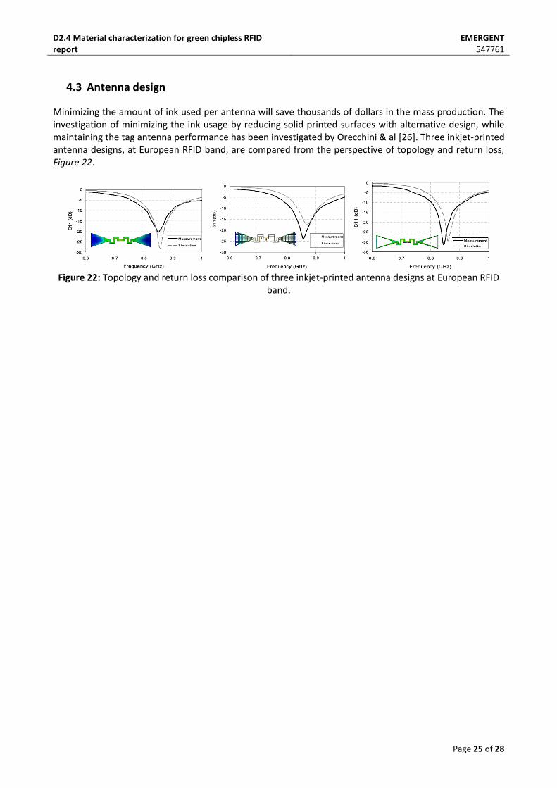
4.3 Antenna design
Minimizing the amount of ink used per antenna will save thousands of dollars in the mass production. The investigation of minimizing the ink usage by reducing solid printed surfaces with alternative design, while maintaining the tag antenna performance has been investigated by Orecchini & al [26]. Three inkjet-printed antenna designs, at European RFID band, are compared from the perspective of topology and return loss, Figure 22.
Figure 22: Topology and return loss comparison of three inkjet-printed antenna designs at European RFID
band.
D2.4 Material characterization for green chipless RFID report
EMERGENT 547761
Page 26 of 28
5 Conclusions
The document initially introduced some basic concepts and techniques aimed at achieving radio frequency sensors with a reduced impact on the environment. The absence of electronics, the integration of the sensors on existing substrates and the use of low-wasting production processes are the main strategies for pursuing those objectives.
A description of some materials and inks considered of potential interest for manufacturing green chipless RFIDs has been presented. In particular, the characterization of a new silver nanoparticle inks in terms of surface impedance has been described in the first part of the document.
Then, a characterization of several dielectric materials potentially used as a substrate for the conductive chipless sensor/tags have been presented. The characterization has been performed by using an accurate cavity resonator approach described in detail in the deliverable 2.3.
Finally, some sheets of paper have been characterized in terms of their sensitivity to environmental variables such as humidity and temperature. Paper is a green material and it is indeed considered an interesting material with a potential twofold role in the design of chipless sensors: it can be used as a substrate for the inkjet printing process and as a sensitive material.
D2.4 Material characterization for green chipless RFID report
EMERGENT 547761
Page 27 of 28
6 References
[1] V. Albino, A. Balice, and R. M. Dangelico, “Environmental strategies and green product development: an overview on sustainability-driven companies,” Business Strategy and the Environment, vol. 18, no. 2, pp. 83–96, Feb. 2009.
[2] L. J. Van der Pauw, “A method of measuring the resistivity and Hall coefficient on lamellae of arbitrary shape,” Philips technical review, vol. 20, no. 8, pp. 220–224, 1958.
[3] H. E. Bussey, “Standards and Measurements of Microwave Surface Impedance, Skin Depth, Conductivity and Q,” IRE Transactions on Instrumentation, vol. I–9, no. 2, pp. 171–175, Sep. 1960.
[4] A. Hernandez, E. Martin, J. Margineda, and J. M. Zamarro, “Resonant cavities for measuring the surface resistance of metals at X-band frequencies,” J. Phys. E: Sci. Instrum., vol. 19, no. 3, p. 222, Mar. 1986.
[5] J. C. Booth, D. H. Wu, and S. M. Anlage, “A broadband method for the measurement of the surface impedance of thin films at microwave frequencies,” Review of Scientific Instruments, vol. 65, no. 6, pp. 2082–2090, Jun. 1994.
[6] I. V. Hyde and W. Milo, “Determining the resistivity of resistive sheets using transmission measurements,” DTIC Document, 2006.
[7] M. W. Hyde, M. J. Havrilla, and P. E. Crittenden, “A Novel Method for Determining the R-Card Sheet Impedance Using the Transmission Coefficient Measured in Free-Space or Waveguide Systems,” IEEE Transactions on Instrumentation and Measurement, vol. 58, no. 7, pp. 2228–2233, Jul. 2009.
[8] J. P. Massman, M. J. Havrilla, K. W. Whites, and M. W. Hyde, “A stepped flange waveguide technique for determining tapered R-card sheet impedance,” in Microwave Conference Proceedings (APMC), 2010 Asia-Pacific, 2010, pp. 1769–1772.
[9] F. Costa, “Surface Impedance Measurement of Resistive Coatings at Microwave Frequencies,” IEEE Transactions on Instrumentation and Measurement, vol. 62, no. 2, pp. 432–437, Feb. 2013.
[10] K. Sarabandi and F. T. Ulaby, “Technique for measuring the dielectric constant of thin materials,” IEEE Transactions on Instrumentation and Measurement, vol. 37, no. 4, pp. 631–636, Dec. 1988.
[11] B. Glover, K. Kirschenmann, and K. W. Whites, “Engineering R-card surface resistivity with printed metallic patterns,” in Proceedings Metamaterials’ 2007 International Congress on Advanced Electr. Materials in Microwaves and Optics, 2007, pp. 621–624.
[12] [10] Datasheet ULTRALAM 3000. RO4000® Series High Frequency Circuit Materials., “[10] Datasheet ULTRALAM 3000. RO4000® Series High Frequency Circuit Materials.”
[13] M. S. Abdul Rahman, S. C. Mukhopadhyay, and P.-L. Yu, Novel Sensors for Food Inspection: Modelling, Fabrication and Experimentation, vol. 10. Cham: Springer International Publishing, 2014.
[14] M. Agarwal, M. D. Balachandran, S. Shrestha, and K. Varahramyan, “SnO 2 Nanoparticle-Based Passive Capacitive Sensor for Ethylene Detection,” Journal of Nanomaterials, vol. 2012, pp. 1–5, 2012.
[15] W. B. Weir, “Automatic measurement of complex dielectric constant and permeability at microwave frequencies,” Proceedings of the IEEE, vol. 62, no. 1, pp. 33–36, Jan. 1974.
[16] K. Marsh and B. Bugusu, “Food Packaging - Roles, Materials, and Environmental Issues,” Journal of Food Science, vol. 72, no. 3, pp. R39–R55, Apr. 2007.
[17] F. Molina-Lopez, D. Briand, and N. F. de Rooij, “All additive inkjet printed humidity sensors on plastic substrate,” Sensors and Actuators B: Chemical, vol. 166–167, pp. 212–222, May 2012.
[18] Y. Amin, J. H\a allstedt, H. Tenhunen, and L.-R. Zheng, “Design of novel paper-based inkjet printed rounded corner bowtie antenna for RFID applications,” Sensors & Transducers Journal, vol. 115, no. 4, pp. 160–167, 2010.
[19] A. Vena, E. Perret, S. Tedjini, G. Eymin Petot Tourtollet, A. Delattre, F. Garet, and Y. Boutant, “Design of Chipless RFID Tags Printed on Paper by Flexography,” IEEE Transactions on Antennas and Propagation, vol. 61, no. 12, pp. 5868–5877, Dec. 2013.
D2.4 Material characterization for green chipless RFID report
EMERGENT 547761
Page 28 of 28
[20] M. Mraović, T. Muck, M. Pivar, J. Trontelj, and A. Pleteršek, “Humidity Sensors Printed on Recycled Paper and Cardboard,” Sensors, vol. 14, no. 8, pp. 13628–13643, Jul. 2014.
[21] A. J. Gimenez, G. Luna-Barcenas, I. C. Sanchez, and J. M. Yanez-Limon, “Paper-Based ZnO Oxygen Sensor,” IEEE Sensors Journal, vol. 15, no. 2, pp. 1246–1251, Feb. 2015.
[22] J. Sarfraz, P. Ihalainen, A. Määttänen, J. Peltonen, and M. Lindén, “Printed hydrogen sulfide gas sensor on paper substrate based on polyaniline composite,” Thin Solid Films, vol. 534, pp. 621–628, May 2013.
[23] T. Jalkanen, A. Määttänen, E. Mäkilä, J. Tuura, M. Kaasalainen, V.-P. Lehto, P. Ihalainen, J. Peltonen, and J. Salonen, “Fabrication of Porous Silicon Based Humidity Sensing Elements on Paper,” Journal of Sensors, vol. 2015, pp. 1–10, 2015.
[24] A. Vásquez Quintero, N. Frolet, D. Marki, A. Marette, G. Mattana, D. Briand, and N. F. De Rooij, “Printing and encapsulation of electrical conductors on polylactic acid (PLA) for sensing applications,” in Micro Electro Mechanical Systems (MEMS), 2014 IEEE 27th International Conference on, 2014, pp. 532–535.
[25] G. Mattana, D. Briand, A. Marette, A. Vásquez Quintero, and N. F. de Rooij, “Polylactic acid as a biodegradable material for all-solution-processed organic electronic devices,” Organic Electronics, vol. 17, pp. 77–86, Feb. 2015.
[26] G. Orecchini, L. Yang, A. Rida, F. Alimenti, M. M. Tentzeris, and L. Roselli, “Green technologies and RFID: Present and future,” Appl. Comput. Electromagn. Soc. J, vol. 25, no. 3, pp. 230–238, 2010.