Embed Size (px)
Citation preview
International Journal of VLSI design & Communication Systems (VLSICS) Vol.6, No.5, October 2015
DOI : 10.5121/vlsic.2015.6506 69
DESIGN OF A COMPACT REVERSIBLE READ-
ONLY-MEMORY WITH MOS TRANSISTORS
Sadia Nowrin, Papiya Nazneen and Lafifa Jamal
Department of Computer Science and Engineering, University of Dhaka, Bangladesh
ABSTRACT
Energy conservative devices are the need of the modern technology which leads to the development of
reversible logic. The synthesis of reversible logic has become an intensely studied area as it overcomes the
problem of power dissipation associated with irreversibility. Storage device such as Read-Only-Memory
(ROM) can be realized in a reversible way with low power dissipation. The reversibility of ROM has not
been yet realized in literature and hence, this paper presents a novel reversible ROM with its
Complementary Metal Oxide Semiconductor (CMOS) realization. On the way to present the architecture of
reversible ROM, we propose a new reversible gate named as Nowrin Papiya (NP) gate. All the proposed
circuits and gates are realized with CMOS based pass transistor logic. Finally, an algorithm as well as
several theorems on the numbers of gates, transistors and garbage outputs have been presented to show
the optimality of the reversible ROM. Simulations using Microwind DSCH software has been shown to
verify the correctness of the proposed design. The comparative results prove that the proposed designs are
efficient and optimized in terms of numbers of gates, transistors, garbage outputs, quantum cost and delay.
KEYWORDS
Reversible ROM, CMOS, Transistor, Garbage Output, Delay, Quantum Cost.
1. INTRODUCTION
Power dissipation that leads to overheating is becoming one of the major issues in today’s world.
The amount of energy dissipated holds a direct relationship to the number of bits erased during
computation. According to R. Landauer’s research [1], traditional computer dissipates KTln2
joules of energy for each bit of information loss, where K is the Boltzmann constant and T is the
operating temperature. Bennett [2] stated that KTln2 Joules of energy would not be dissipated if
the computation is carried out in a reversible way. That gave rise to reversible logic circuit which
does not erase information and input vector can be uniquely reconstructed from the output vector.
In recent years, reversible logic has gained attention in low power CMOS design [2], quantum
computing, nanotechnology, quantum dot cellular automata, cryptography etc. Zhirnov et al. [3]
proved that power dissipation in any future CMOS will lead to an impossible heat removal
problem. The number of transistors will double every 18 months according to Gordon Moore [4].
However, if Zhirnov and Moore’s Law will continue to be in effect, speeding-up of CMOS
devices will be impossible at some point in 2020 or earlier.
International Journal of VLSI design & Communication Systems (VLSICS) Vol.6, No.5, October 2015
70
In this work, we present the design methodologies of a compact reversible ROM with its CMOS
realization. To the best of our knowledge, this is the first work to realize reversible ROM with
MOS transistors. We propose different components of reversible ROM with their transistor
design and finally, we propose the reversible architecture of ROM. All the proposed circuits are
optimized in terms of gate count, transistor count, garbage output, quantum cost and delay.
2. LITERATURE REVIEW
This section presents the basic ideas and theories of reversible logic with some popular reversible
gates which are relevant to this research work.
2.1 Reversible Gate
A reversible logic gate is an n-input, n-output circuit having a unique output pattern [5] for each
possible input pattern. There is a one-to-one mapping between inputs and outputs. Thus, an n×n
reversible logic gate can be represented as Iv ↔ Ov, where, Iv = (I1, I2, I3, …, In−1, In) is the input
vector and Ov = (O1, O2, O3, ..., On−1, On) is the output vector.
2.2 Optimization Issues
The main challenge of designing a reversible circuit is to optimize different cost metrics or
parameters as follows:
2.2.1 Number of Gates
The total number of gates used in a circuit. A reversible circuit must use minimum possible
number of gates.
2.2.2 Constant Inputs
The inputs that are added to an n×k function to make it reversible are called constant inputs. The
number of constant inputs should be minimum to design reversible logic circuits.
2.2.3 Garbage Outputs
Unwanted or unused outputs of a reversible gate or circuit required to maintain reversibility are
known as garbage outputs [5].
2.2.4 Quantum Cost
One of the most important challenges in reversible logic design is to optimize quantum cost. The
quantum cost can be derived by substituting the reversible logic gates of a circuit by a cascade of
elementary quantum gates [6]. Elementary quantum gates realize quantum circuits that are
inherently reversible and manipulate qubits rather than pure logic values [7]. The state of a qubit
for two pure logic states can be expressed like |Ψ> = α |0> + β |1>, where |0> and |1> denote 0
and 1, respectively, and α and β are complex numbers such that |α|2 + |β|
2 = 1. The most used
elementary quantum gates are the NOT gate (a single qubit is inverted), the controlled-NOT
International Journal of VLSI design & Communication Systems (VLSICS) Vol.6, No.5, October 2015
71
(CNOT) gate (the target qubit is inverted if the single control qubit is 1), the controlled-V gate
(also known as a square root of NOT, since two consecutive V operations are equivalent to an
inversion), and the controlled V+ gate (which performs the inverse operation of the V gate and
thus is also a square root of NOT) [7].
2.2.5 Delay
The delay of a logic circuit is the maximum number of gates in a path from any input line to the
output line [8]. According to [9], [10], the delay of any 3× 3 reversible gate can be computed by
calculating its logical depth when it is designed from smaller 1×1 and 2× 2 reversible gates with
unit delay. It is denoted by ∆. For example, the Fredkin gate requires 5∆ delay [9]. In this
research work, we consider the logical depth as a measure of delay.
2.3 Popular Reversible Logic Gates
In this section, we present the basic reversible logic gates which are related to our research work.
2.3.1 Feynman Gate
Feynman gate [11] is a 2× 2 reversible gate that maps two inputs (A, B) to two outputs (P = A, Q
= A⊕ B). Since this is a 2×2 gate, the quantum cost is 1 [11].
2.3.2 Fredkin Gate
Fredkin gate [12] is a 3×3 reversible gate that maps three inputs (A, B, C) to three outputs (P = A,
Q = A′B⊕ AC, R = A′C⊕ AB). The quantum cost of Fredkin gate is 5 [12].
2.3.3 Toffoli Gate
Toffoli gate [13] is a 3×3 reversible gate with the mapping of (A, B, C) to (P = A, Q = B, R = AB
⊕ C), where A, B, C are the inputs and P, Q, R are the outputs. The quantum cost of Toffoli gate
is 5 [13].
2.3.4 HL Gate
HL gate [14] is a 4×4 reversible gate that maps four inputs (A, B, C, D) to four outputs (P = AB′
⊕ B′C ⊕ BD′, Q = AB ⊕ B′C ⊕ BD, R = A′B ⊕ B′C ⊕ BD and S = AB′ ⊕ BC ⊕ B′D). The
quantum cost of HL gate is 7 [14].
3. BACKGROUND STUDY
A ROM that can store 2
n words each of m bit is referred to as 2
n×m bit ROM, where n is the
number of address inputs and m is the number of data bits. A 2n × m ROM requires one k-to-2
k
row decoder, one (n-k)-to-2(n−k)
column decoder, 2n registers each consists of m number of D FFs
to store data inputs and finally the output buffer to store the data outputs. There is no existing
design of reversible ROM in literature. But, the components (Reversible Decoder and D FF) have
been realized by many researchers. If the components are designed in an optimized way, the final
International Journal of VLSI design & Communication Systems (VLSICS) Vol.6, No.5, October 2015
72
design of reversible ROM will also be optimized. Various transistor design of reversible decoder
have been proposed in [15,16]. Shamsujjoha and Babu [15] proposed the transistor design of a
fault tolerant reversible decoder which requires a large number of transistors. Ravish et al. [16]
only mentioned the transistor count of a reversible decoder without showing the transistor design
and it requires more transistors than [16]. Different approaches of reversible D FF have been
proposed in [5,8,10,17–19]. Mamun et al. [17] proposed a reversible D FF which shows no
design for the complement output Q′. Existing reversible D FFs in [5,8,10,18] requires large
number of gates, quantum cost and delay. Thapliyal and Vinod [19] proposed the transistor
design of a reversible D latch. But the [19] design for the complement output requires more
quantum cost than other existing designs.
4. PROPOSED TRANSISTOR REALIZATION OF REVERSIBLE GATES
In this section, we propose the transistor implementation of reversible logic gates that are
required to design the components of reversible ROM.
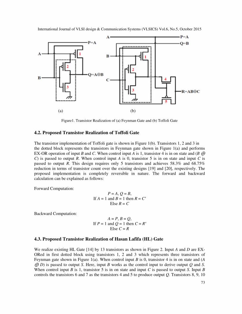
4.1. Proposed Transistor Realization of Feynman Gate
The transistor implementation of reversible Feynman gate is shown in Figure 1(a). When control
input A is 0, transistor 1 is in on state and input B is passed straight to output Q. When control
input A is 1, transistor 2 and transistor 3 are in on state and input B is inverted to pass to output Q.
This design requires only 3 transistors and achieves 62.5% reduction over the existing designs
[19] and [20] in terms of transistor count. Our proposed implementation is completely reversible
in nature as it is suitable for both forward and backward computation.
Forward Computation:
P = A,
If A = 0 then Q = B
Else Q = B′
Backward Computation:
A = P,
If P = 0 then B = Q
Else B = Q′
International Journal of VLSI design & Communication Systems (VLSICS) Vol.6, No.5, October 2015
73
(a) (b)
Figure1. Transistor Realization of (a) Feynman Gate and (b) Toffoli Gate
4.2. Proposed Transistor Realization of Toffoli Gate
The transistor implementation of Toffoli gate is shown in Figure 1(b). Transistors 1, 2 and 3 in
the dotted block represents the transistors in Feynman gate shown in Figure 1(a) and performs
EX-OR operation of input B and C. When control input A is 1, transistor 4 is in on state and (B ⊕
C) is passed to output R. When control input A is 0, transistor 5 is in on state and input C is
passed to output R. This design requires only 5 transistors and achieves 58.3% and 68.75%
reduction in terms of transistor count over the existing designs [19] and [20], respectively. The
proposed implementation is completely reversible in nature. The forward and backward
calculation can be explained as follows:
Forward Computation:
P = A, Q = B,
If A = 1 and B = 1 then R = C′
Else R = C
Backward Computation:
A = P, B = Q,
If P = 1 and Q = 1 then C = R′
Else C = R
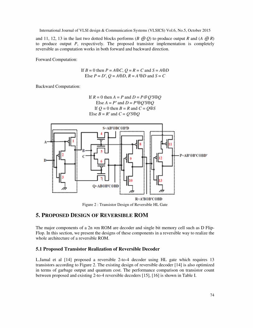
4.3. Proposed Transistor Realization of Hasan Lafifa (HL) Gate
We realize existing HL Gate [14] by 13 transistors as shown in Figure 2. Input A and D are EX-
ORed in first dotted block using transistors 1, 2 and 3 which represents three transistors of
Feynman gate shown in Figure 1(a). When control input B is 0, transistor 4 is in on state and (A
⊕ D) is passed to output S. Here, input B works as the control input to derive output Q and S.
When control input B is 1, transistor 5 is in on state and input C is passed to output S. Input B
controls the transistors 6 and 7 as the transistors 4 and 5 to produce output Q. Transistors 8, 9, 10
International Journal of VLSI design & Communication Systems (VLSICS) Vol.6, No.5, October 2015
74
and 11, 12, 13 in the last two dotted blocks performs (B ⊕ Q) to produce output R and (A ⊕ R)
to produce output P, respectively. The proposed transistor implementation is completely
reversible as computation works in both forward and backward direction.
Forward Computation:
If B = 0 then P = A⊕C, Q = R = C and S = A⊕D
Else P = D′, Q = A⊕D, R = A′⊕D and S = C
Backward Computation:
If R = 0 then A = P and D = P⊕ Q′S⊕Q
Else A = P′ and D = P′⊕Q′S⊕Q
If Q = 0 then B = R and C = Q⊕S
Else B = R′ and C = Q′S⊕Q
Figure 2 : Transistor Design of Reversible HL Gate
5. PROPOSED DESIGN OF REVERSIBLE ROM
The major components of a 2n ×m ROM are decoder and single bit memory cell such as D Flip-
Flop. In this section, we present the designs of these components in a reversible way to realize the
whole architecture of a reversible ROM.
5.1 Proposed Transistor Realization of Reversible Decoder
L.Jamal et al [14] proposed a reversible 2-to-4 decoder using HL gate which requires 13
transistors according to Figure 2. The existing design of reversible decoder [14] is also optimized
in terms of garbage output and quantum cost. The performance comparison on transistor count
between proposed and existing 2-to-4 reversible decoders [15], [16] is shown in Table I.
International Journal of VLSI design & Communication Systems (VLSICS) Vol.6, No.5, October 2015
75
Table 1 : Comparison of Reversible 2-To-4 Decoders
Circuit Transistor Count
Proposed Circuit 13
Existing Circuit [15] 20
Existing Circuit [16] 24
Improvement(%)w.r.t [15] 35
Improvement(%)w.r.t [16] 45.83
A 3-to-8 reversible decoder can be realized by applying four outputs of a 2-to-4 reversible
decoder to four separate Fredkin gates. So, a generalized n-to-2n reversible decoder needs one
(k-1)-to-2k−1
reversible decoder with additional 2k−1
number of Fredkin gates.
Theorem 1: If T is the total number of transistors to design an n-to-2n reversible decoder, then T
= 4×2n – 3.
Proof: We prove the above statement by induction:
According to our design, a 2-to-4 reversible decoder requires 13 (= 4×22-3) transistors. So, the
statement holds for base n = 2.
Assume for n = k, a k-to-2k reversible decoder can be realized by 4×2
k -3 no. of transistors.
Now, a (k+1)-to-2k+1
decoder contains a k-to-2k decoder with 2
k number of Fredkin gates. Each
Fredkin gate requires 4 transistors [19] resulting in total:
T = (4×2k -3) + 4× 2
k
= 4×2k+1
-3
Thereby, the statement holds for n = k + 1.
So, If T is the total number of transistors to design an n-to-2n reversible decoder, then T = 4×2
n -
3.
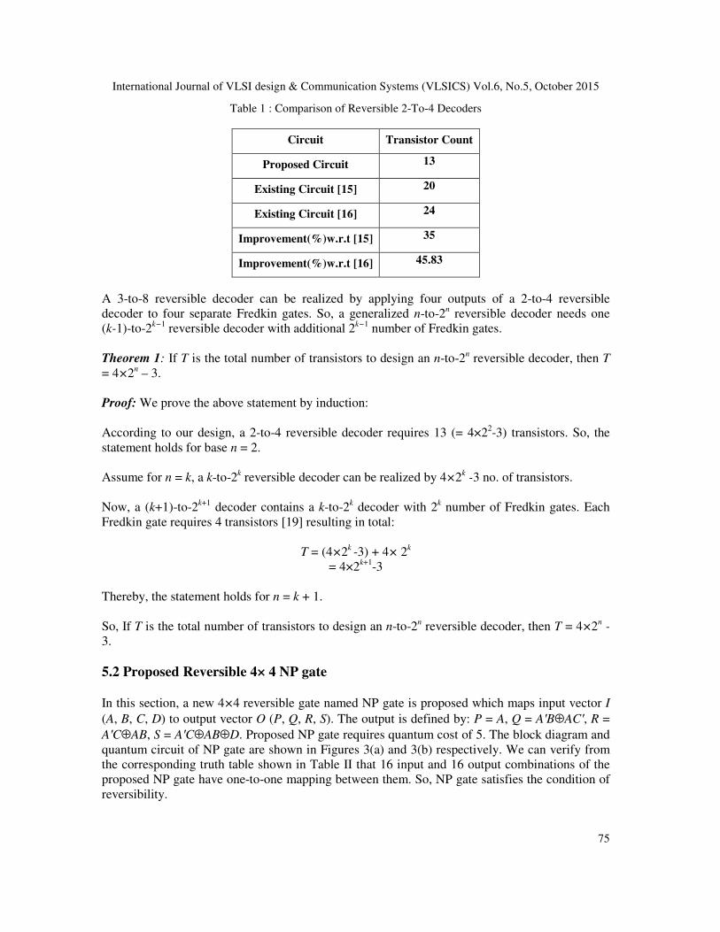
5.2 Proposed Reversible 4× 4 NP gate
In this section, a new 4×4 reversible gate named NP gate is proposed which maps input vector I
(A, B, C, D) to output vector O (P, Q, R, S). The output is defined by: P = A, Q = A′B⊕AC′, R =
A′C⊕AB, S = A′C⊕AB⊕D. Proposed NP gate requires quantum cost of 5. The block diagram and
quantum circuit of NP gate are shown in Figures 3(a) and 3(b) respectively. We can verify from
the corresponding truth table shown in Table II that 16 input and 16 output combinations of the
proposed NP gate have one-to-one mapping between them. So, NP gate satisfies the condition of
reversibility.
International Journal of VLSI design & Communication Systems (VLSICS) Vol.6, No.5, October 2015
76
(a) (b)
Figure3. (a) Block Diagram and (b) Quantum Circuit of NP gate
Table 2: Truth Table of NP Gate
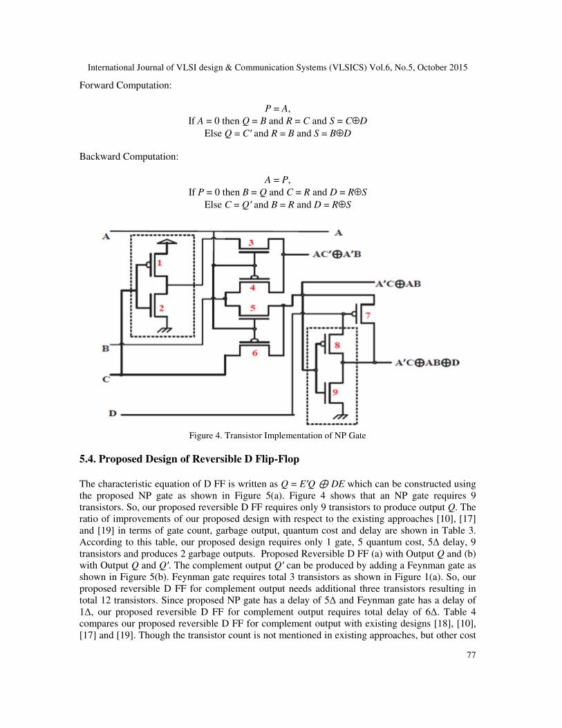
5.3. Transistor Realization of NP Gate
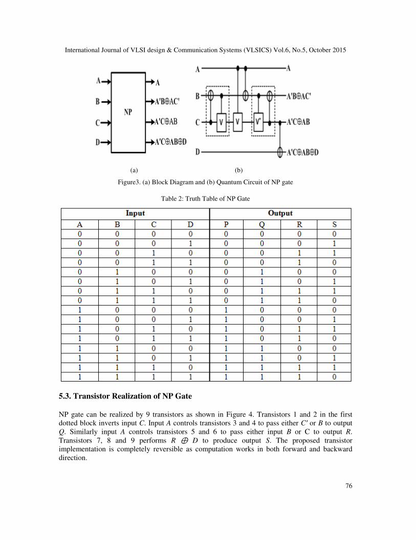
NP gate can be realized by 9 transistors as shown in Figure 4. Transistors 1 and 2 in the first
dotted block inverts input C. Input A controls transistors 3 and 4 to pass either C′ or B to output
Q. Similarly input A controls transistors 5 and 6 to pass either input B or C to output R.
Transistors 7, 8 and 9 performs R ⊕ D to produce output S. The proposed transistor
implementation is completely reversible as computation works in both forward and backward
direction.
International Journal of VLSI design & Communication Systems (VLSICS) Vol.6, No.5, October 2015
77
Forward Computation:
P = A,
If A = 0 then Q = B and R = C and S = C⊕D
Else Q = C′ and R = B and S = B⊕D
Backward Computation:
A = P,
If P = 0 then B = Q and C = R and D = R⊕S
Else C = Q′ and B = R and D = R⊕S
Figure 4. Transistor Implementation of NP Gate
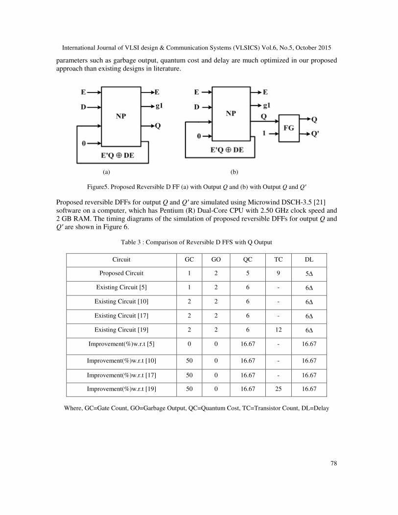
5.4. Proposed Design of Reversible D Flip-Flop
The characteristic equation of D FF is written as Q = E′Q ⊕ DE which can be constructed using
the proposed NP gate as shown in Figure 5(a). Figure 4 shows that an NP gate requires 9
transistors. So, our proposed reversible D FF requires only 9 transistors to produce output Q. The
ratio of improvements of our proposed design with respect to the existing approaches [10], [17]
and [19] in terms of gate count, garbage output, quantum cost and delay are shown in Table 3.
According to this table, our proposed design requires only 1 gate, 5 quantum cost, 5∆ delay, 9
transistors and produces 2 garbage outputs. Proposed Reversible D FF (a) with Output Q and (b)
with Output Q and Q′. The complement output Q′ can be produced by adding a Feynman gate as
shown in Figure 5(b). Feynman gate requires total 3 transistors as shown in Figure 1(a). So, our
proposed reversible D FF for complement output needs additional three transistors resulting in
total 12 transistors. Since proposed NP gate has a delay of 5∆ and Feynman gate has a delay of
1∆, our proposed reversible D FF for complement output requires total delay of 6∆. Table 4
compares our proposed reversible D FF for complement output with existing designs [18], [10],
[17] and [19]. Though the transistor count is not mentioned in existing approaches, but other cost
International Journal of VLSI design & Communication Systems (VLSICS) Vol.6, No.5, October 2015
78
parameters such as garbage output, quantum cost and delay are much optimized in our proposed
approach than existing designs in literature.
(a) (b)
Figure5. Proposed Reversible D FF (a) with Output Q and (b) with Output Q and Q′
Proposed reversible DFFs for output Q and Q′ are simulated using Microwind DSCH-3.5 [21]
software on a computer, which has Pentium (R) Dual-Core CPU with 2.50 GHz clock speed and
2 GB RAM. The timing diagrams of the simulation of proposed reversible DFFs for output Q and
Q′ are shown in Figure 6.
Table 3 : Comparison of Reversible D FFS with Q Output
Circuit GC GO QC TC DL
Proposed Circuit 1 2 5 9 5∆
Existing Circuit [5] 1 2 6 - 6∆
Existing Circuit [10] 2 2 6 - 6∆
Existing Circuit [17] 2 2 6 - 6∆
Existing Circuit [19] 2 2 6 12 6∆
Improvement(%)w.r.t [5] 0 0 16.67 - 16.67
Improvement(%)w.r.t [10] 50 0 16.67 - 16.67
Improvement(%)w.r.t [17] 50 0 16.67 - 16.67
Improvement(%)w.r.t [19] 50 0 16.67 25 16.67
Where, GC=Gate Count, GO=Garbage Output, QC=Quantum Cost, TC=Transistor Count, DL=Delay
International Journal of VLSI design & Communication Systems (VLSICS) Vol.6, No.5, October 2015
79
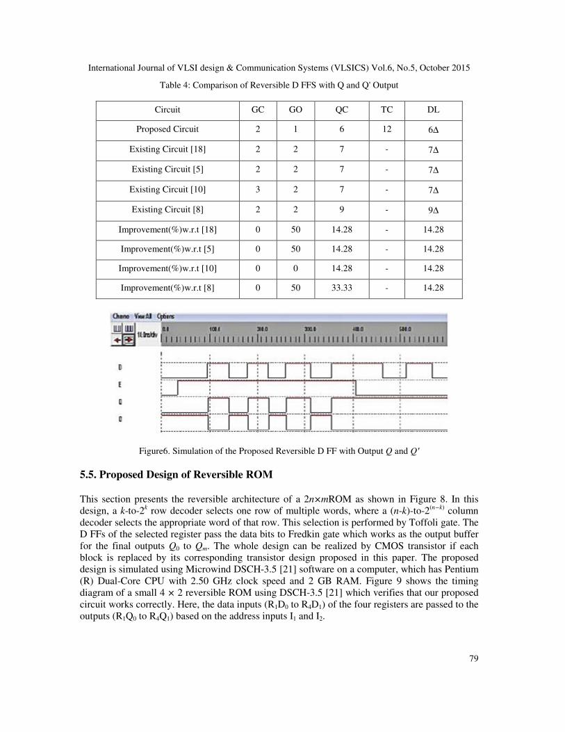
Table 4: Comparison of Reversible D FFS with Q and Q' Output
Circuit GC GO QC TC DL
Proposed Circuit 2 1 6 12 6∆
Existing Circuit [18] 2 2 7 - 7∆
Existing Circuit [5] 2 2 7 - 7∆
Existing Circuit [10] 3 2 7 - 7∆
Existing Circuit [8] 2 2 9 - 9∆
Improvement(%)w.r.t [18] 0 50 14.28 - 14.28
Improvement(%)w.r.t [5] 0 50 14.28 - 14.28
Improvement(%)w.r.t [10] 0 0 14.28 - 14.28
Improvement(%)w.r.t [8] 0 50 33.33 - 14.28
Figure6. Simulation of the Proposed Reversible D FF with Output Q and Q′
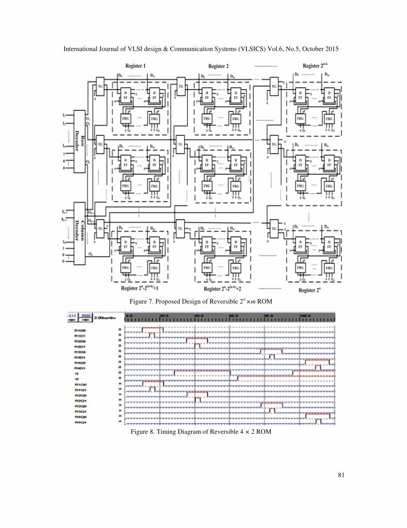
5.5. Proposed Design of Reversible ROM
This section presents the reversible architecture of a 2n×mROM as shown in Figure 8. In this
design, a k-to-2k row decoder selects one row of multiple words, where a (n-k)-to-2
(n−k) column
decoder selects the appropriate word of that row. This selection is performed by Toffoli gate. The
D FFs of the selected register pass the data bits to Fredkin gate which works as the output buffer
for the final outputs Q0 to Qm. The whole design can be realized by CMOS transistor if each
block is replaced by its corresponding transistor design proposed in this paper. The proposed
design is simulated using Microwind DSCH-3.5 [21] software on a computer, which has Pentium
(R) Dual-Core CPU with 2.50 GHz clock speed and 2 GB RAM. Figure 9 shows the timing
diagram of a small 4 × 2 reversible ROM using DSCH-3.5 [21] which verifies that our proposed
circuit works correctly. Here, the data inputs (R1D0 to R4D1) of the four registers are passed to the
outputs (R1Q0 to R4Q1) based on the address inputs I1 and I2.
International Journal of VLSI design & Communication Systems (VLSICS) Vol.6, No.5, October 2015
80
International Journal of VLSI design & Communication Systems (VLSICS) Vol.6, No.5, October 2015
81
Figure 7. Proposed Design of Reversible 2n ×m ROM
Figure 8. Timing Diagram of Reversible 4 × 2 ROM
International Journal of VLSI design & Communication Systems (VLSICS) Vol.6, No.5, October 2015
82
Theorem 2: A 2n×m Reversible ROM can be realized by 2
k + 2
n(2
−k + 2m + 1) - 6 gates where n
be the number of address input and m be the data bit.
Proof: A 2n × m reversible ROM contains one k-to-2
k row decoder and one (n-k)-to-2
n−k column
decoder. According to theorem presented in [14], total gates needed in decoder part is:
2k - 3 + 2
n−k – 3
= 2k + 2
n−k - 6.
Each of the 2n registers consists of m number of D FFs and each D FF needs one NP gate
resulting in total m×2n D FFs. In addition, The ROM requires 2
n Toffoli gates and m× 2
n Fredkin
gates for AND and COPY operation. Therefore, total gate count is:
2k + 2
n−k - 6 + (m × 2
n) + 2
n + (m × 2
n)
= 2k + 2
n(2
−k + 2m + 1) - 6
Theorem 3: A 2n×m Reversible ROM generates n+2
k+ 2
n(2m+2
−k +1) - 4 garbage outputs where
n is the number of address input and m is the data bit.
Proof: According to [14], Garbage outputs produced from decoder part is k - 2 + n - k - 2 = n - 4.
According to our design, Toffoli gates from the last row and last column generates one garbage
except the last one producing two garbages which results in total 2k-1+2
n−k- 1+2 = 2
k +2
n−k
garbage outputs. Each of the m× 2n D FFs generates one garbage bit.
Again, among (2n × m) Fredkin gates, 2
n Fredkin gates produces two garbages and rest of the (2
n
× m - 2n) produce one garbage resulting in total 2×2
n +2
n ×m - 2
n = 2
n (m+1) garbages.
So, total garbages produced from a reversible ROM is:
n - 4 + m × 2n + 2
k + 2
n−k + 2
n (m + 1)
=n + 2k + 2
n (2m + 2
−k + 1) - 4
Theorem 4: If T is the total transistor count for a 2n×m Reversible ROM, then T = 2
n (4×2
−k
+13m+5)+4 × 2k - 6.
Proof: According to Theorem 1, the number of transistors in decoder part :
(4 × 2k - 3 + 4 × 2
n−k - 3) = 4 × 2
k + 4 × 2
n −k
– 6.
Each of the (m × 2n) D FFs requires 9 transistors resulting in total 9 (m × 2
n) transistors.
Again, there are 2n Toffoli gates each having 5 transistors and (2
n ×m) Fredkin gates each having
4 transistors resulting in total 2n (5 + 4m) transistors. So,
T = 4×2k + 4×2
n−k - 6+9(m×2
n) +2
n(5+4m)
=2n(4 × 2
−k + 13m + 5) + 4 × 2
k - 6
International Journal of VLSI design & Communication Systems (VLSICS) Vol.6, No.5, October 2015
83
6. CONCLUSIONS
In this paper, we presented the design methodologies of a novel reversible ROM. This is the first
reversible design of ROM where gate count, transistor count and garbage output are optimized.
For example, our proposed reversible 16×2 ROM requires 82 reversible gates, 522 transistors and
produces only 18 garbage outputs. Similarly, our proposed reversible 16 × 4 ROM requires 146
reversible gates, 938 transistors and produces only 152 garbage outputs. We proposed the core
components with optimum gate count, garbage outputs, quantum cost, delay and transistor count.
In addition, we realized each component and related gates using MOS transistors. We also proved
the efficiency of the proposed circuits by comparative results, theorems and algorithms.
Simulation results showed the correctness of the proposed circuits.
Proposed reversible ROM can be used in Bootstrap memory, Embedded Microcontroller Program
Memory, Firmware, Data Tables, Data Converter, Function Generator [22] etc.
ACKNOWLEDGEMENTS
This work was done under the assistance of MOICT (Ministry of ICT) Fellowship given by the
Ministry of ICT, Government of the People’s Republic of Bangladesh.
REFERENCES [1] R. Landauer, “Irreversibility and Heat Generation in the Computing Process”, IBM journal of
research and development, vol. 5, pp. 183-191, 1961.
[2] C. H. Bennett, “Logical Reversibility of Computation”, IBM journal of Research and Development,
vol. 17, pp. 525-232, 1973.
[3] V. Zhirnov, R. Cavin, J. Hutchby, G. Bourianoff, “Limits to Binary Logic Switch Scaling –a
Gedanken Model”, Proceedings of the IEEE, vol. 91, pp. 1934-1939, 2003.
[4] G. E. Moore, “Cramming more components onto integrated circuits”, Electronics, vol. 38, pp. 56-59,
1965.
[5] A.S.M. Sayem, M. Ueda, “Optimization of reversible sequential circuits”, Journal of Computing, vol.
38, pp. 208-214, 2010.
[6] M.A. Nielsen, I.L. Chuang, “Quantum computation and quantum information”, Cambridge university
press, 2010.
[7] R. Wille, R. Drechsler, “BDD-based synthesis of reversible logic for large functions”, Proceedings of
the 46th Annual Design Automation Conference, pp. 270–275. 2009.
[8] N. Nayeem, M. Hossain, L. Jamal, H. Babu, “Efficient Design of Shift Registers Using Reversible
Logic”, International Conference on Signal Processing Systems, pp. 474–478, 2009.
[9] M. Mohammadi, M.; M. Eshghi, “On figures of merit in reversible and quantum logic designs”,
Quantum Information Processing, vol. 8, pp. 297-318. 2009.
[10] H. Thapliyal, N. Ranganathan, “Design of Reversible Latches Optimized for Quantum Cost, Delay
and Garbage Outputs”, VLSID ’10. 23rd International Conference on, pp. 235-240, 2010.
[11] R.P. Feynman, “Quantum mechanical computers”, Foundations of physics, vol. 16, pp. 507–531,
1986.
[12] E. Fredkin, T. Toffoli, “Conservative logic”, Springer, 2002.
[13] T. Toffoli, “Reversible computing”, Springer, 1980.
[14] L. Jamal, M. Alam, H.M.Hasan Babu, “An efficient approach to design a reversible control unit of a
processor”, Sustainable Computing: Informatics and Systems, vol. 3, pp. 286-294, 2013.
[15] M. Shamsujjoha, H. Babu, “A Low Power Fault Tolerant Reversible Decoder Using MOS
Transistors”, International Conference on Embedded Systems and VLSI Design (VLSID), pp. 368–
373, 2013.
International Journal of VLSI design & Communication Systems (VLSICS) Vol.6, No.5, October 2015
84
[16] H.V.R. Aradhya, R. Chinmaye, K.N. Muralidhara, “Design, Optimization and Synthesis of Efficient
Reversible Logic Binary Decoder”, International Journal of Computer Applications, vol. 46, pp. 45–
51, 2012.
[17] M.S.Al Mamun, I. Manda, M. Hasanuzzaman, “Design of Universal Shift Register Using Reversible
Logic”, International Journal of Engineering and Technology, vol. 2, pp. 1620–1625, 2012.
[18] L. Jamal, F. Sharmin, M.A.Mottalib, H.M.H. Babu, “Design and Minimization of Reversible Circuits
for a Data Acquisition and Storage System”, International Journal of Engineering and Technology,
vol. 2, pp. 9-15, 2012.
[19] H. Thapliyal, A. Vinod, “Design of reversible sequential elements with feasibility of transistor
implementation”, IEEE International Symposium on Circuits and Systems, ISCAS, pp. 625–628,
2007.
[20] Y. Van Rentergem, A. De Vos, “Optimal design of a reversible full adder”, International Journal of
Unconventional Computing, vol. 1, pp. 339–355, 2005.
[21] DSCH: Microwind and DSCH information page.[Online].Available: http://www.microwind.org.
[22] R.J. Tocci, “Digital Systems: principles and applications”, Prentice Hall, 1980.
AUTHORS Sadia Nowrin obtained her M.S. degree in Computer Science and Engineering from University of Dhaka,
Bangladesh in 2015. .
Papiya Nazneen received a B.Sc degree in Computer Science and Engineering from University of Dhaka,
Bangladesh in 2013.
Lafifa Jamal is currently working as an Associate Professor at the Department of Computer Science and
Engineering, University of Dhaka. She received her B.Sc. and M.Sc. degrees in Computer Science from
University of Dhaka, Bangladesh. She is currently pursuing her PhD in the same department. Her research
interests include VLSI Design, Logic Synthesis and Design, Reversible Logic, FPGA Design and Quantum
Computing. She is a member of IEEE.