Embed Size (px)
Citation preview

CYUSB303X
EZ-USB® FX3S SuperSpeed USB Controller
Cypress Semiconductor Corporation • 198 Champion Court • San Jose, CA 95134-1709 • 408-943-2600Document Number: 001-84160 Rev. *F Revised January 14, 2016
EZ-USB® FX3S SuperSpeed USB Controller
Features
Universal serial bus (USB) integration USB 3.0 and USB 2.0 peripherals compliant with USB 3.0
specification 1.0 5-Gbps USB 3.0 PHY compliant with PIPE 3.0 High-speed On-The-Go (HS-OTG) host and peripheral
compliant with OTG Supplement Version 2.0 Thirty-two physical endpoints Support for battery charging Spec 1.1 and accessory charger
adaptor (ACA) detection
General Programmable Interface (GPIF™ II) Programmable 100-MHz GPIF II enables connectivity to a
wide range of external devices 8- and 16-bit data bus As many as 16 configurable control signals
Mass storage support SD 3.0 (SDXC) UHS-1 eMMC 4.41 Two ports that can support memory card sizes up to 2TB Built-in RAID with support for RAID0 and RAID1
System I/O expansion with two secure digital I/O (SDIO 3.0) ports
Support for USB-attached storage (UAS), mass-storage class (MSC), human interface device (HID), full, and Turbo-MTP™
Fully accessible 32-bit CPU ARM926EJ core with 200-MHz operation 512-KB or 256-KB embedded SRAM
Additional connectivity to the following peripherals I2C master controller at 1 MHz I2S master (transmitter only) at sampling frequencies of
32 kHz, 44.1 kHz, and 48 kHz UART support of up to 4 Mbps SPI master at 33 MHz
Selectable clock input frequencies 19.2, 26, 38.4, and 52 MHz 19.2-MHz crystal input support
Ultra low-power in core power-down mode Less than 60 µA with VBATT on 20 µA with VBATT off
Independent power domains for core and I/O Core operation at 1.2 V I2S, UART, and SPI operation at 1.8 to 3.3 V I2C operation at 1.2 V
10-mm × 10-mm, 0.8-mm pitch Pb-free ball grid array (BGA) package
EZ-USB® software and development kit (DVK) for easy code development
Applications
Digital video camcorders
Digital still cameras
Printers
Scanners
Video capture cards
Test and measurement equipment
Surveillance cameras
Personal navigation devices
Medical imaging devices
Video IP phones
Portable media players
Industrial cameras
RAID controller
USB Disk on Module
Functional Description
For a complete list of related resources, click here.
Logic Block Diagram

CYUSB303X
Document Number: 001-84160 Rev. *F Page 2 of 54
More InformationCypress provides a wealth of data at www.cypress.com to help you to select the right <product> device for your design, and to helpyou to quickly and effectively integrate the device into your design. For a comprehensive list of resources, see the knowledge basearticle KBA87889, How to design with FX3/FX3S.
Overview: USB Portfolio, USB Roadmap
USB 3.0 Product Selectors: FX3, FX3S, CX3, HX3, West Bridge Benicia
Application notes: Cypress offers a large number of USB appli-cation notes covering a broad range of topics, from basic to advanced level. Recommended application notes for getting started with FX3 are: AN75705 - Getting Started with EZ-USB FX3 AN76405 - EZ-USB FX3 Boot Options AN70707 - EZ-USB FX3/FX3S Hardware Design Guidelines
and Schematic Checklist AN65974 - Designing with the EZ-USB FX3 Slave FIFO In-
terface AN75779 - How to Implement an Image Sensor Interface with
EZ-USB FX3 in a USB Video Class (UVC) Framework AN86947 - Optimizing USB 3.0 Throughput with EZ-USB
FX3 AN84868 - Configuring an FPGA over USB Using Cypress
EZ-USB FX3 AN68829 - Slave FIFO Interface for EZ-USB FX3: 5-Bit Ad-
dress Mode
AN73609 - EZ-USB FX2LP/ FX3 Developing Bulk-Loop Ex-ample on Linux
AN77960 - Introduction to EZ-USB FX3 High-Speed USB Host Controller
AN76348 - Differences in Implementation of EZ-USB FX2LP and EZ-USB FX3 Applications
AN89661 - USB RAID 1 Disk Design Using EZ-USB FX3S
Code Examples: USB Hi-Speed USB Full-Speed USB SuperSpeed
Technical Reference Manual (TRM): EZ-USB FX3 Technical Reference Manual
Development Kits: CYUSB3KIT-003, EZ-USB FX3 SuperSpeed Explorer Kit CYUSB3KIT-001, EZ-USB FX3 Development Kit
Models: IBIS
EZ-USB FX3 Software Development Kit
Cypress delivers the complete software and firmware stack for FX3, in order to easily integrate SuperSpeed USB into any embedded application. The Software Development Kit (SDK) comes with tools, drivers and application examples, which help accelerate appli-cation development.
GPIF™ II Designer
The GPIF II Designer is a graphical software that allows designers to configure the GPIF II interface of the EZ-USB FX3 USB 3.0 Device Controller.
The tool allows users the ability to select from one of five Cypress supplied interfaces, or choose to create their own GPIF II interface from scratch. Cypress has supplied industry standard interfaces such as asynchronous and Synchronous Slave FIFO, Asynchronous and Synchronous SRAM, and Asynchronous SRAM. Designers who already have one of these pre-defined interfaces in their system can simply select the interface of choice, choose from a set of standard parameters such as bus width (x8, 16, x32) endianess, clock settings, and compile the interface. The tool has a streamlined three step GPIF interface development process for users who need a customized interface. Users are able to first select their pin configuration and standard parameters. Secondly, they can design a virtual state machine using configurable actions. Finally, users can view output timing to verify that it matches the expected timing. Once the three step process is complete, the interface can be compiled and integrated with FX3.

CYUSB303X
Document Number: 001-84160 Rev. *F Page 3 of 54
Contents
Functional Overview ..........................................................4Application Examples ....................................................4
USB Interface ......................................................................5OTG ...............................................................................5ReNumeration ...............................................................6EZ-Dtect ........................................................................6VBUS Overvoltage Protection .......................................6Carkit UART Mode ........................................................6
Host Processor Interface (P-Port) .....................................7GPIF II ...........................................................................7Slave FIFO Interface .....................................................7Asynchronous SRAM ....................................................7Asynchronous Address/Data Multiplexed ......................8Synchronous ADMux Interface ......................................8Processor MMC (PMMC) Slave Interface .....................8
CPU ....................................................................................10
Storage Port (S-Port) ........................................................10SD/MMC Clock Stop ...................................................10SD_CLK Output Clock Stop ........................................10Card Insertion and Removal Detection .......................10Write Protection (WP) ..................................................10SDIO Interrupt .............................................................10SDIO Read-Wait Feature ............................................10
JTAG Interface ..................................................................11
Other Interfaces ................................................................11UART Interface ............................................................11I2C Interface ................................................................11I2S Interface ................................................................11SPI Interface ................................................................11
Boot Options .....................................................................12
Reset ..................................................................................12Hard Reset ..................................................................12Soft Reset ....................................................................12
Clocking ............................................................................1332-kHz Watchdog Timer Clock Input ...........................13
Power .................................................................................14Power Modes ..............................................................14
Configuration Options .....................................................17
Digital I/Os .........................................................................17
GPIOs .................................................................................17
System-level ESD .............................................................17
Pin Description .................................................................18
Absolute Maximum Ratings ............................................22
Operating Conditions .......................................................22
DC Specifications .............................................................22
AC Timing Parameters .....................................................24GPIF II Timing .............................................................24Asynchronous SRAM Timing ......................................27ADMux Timing for Asynchronous Access ...................30Synchronous ADMux Timing .......................................32Slave FIFO Interface ...................................................35Asynchronous Slave FIFO
Read Sequence Description ...............................................37Asynchronous Slave FIFO
Write Sequence Description ...............................................38Storage Port Timing ....................................................41Serial Peripherals Timing ............................................44
Reset Sequence ................................................................49
Package Diagram ..............................................................50
Ordering Information ........................................................51Ordering Code Definitions ...........................................51
Acronyms ..........................................................................52
Document Conventions ...................................................52Units of Measure .........................................................52
Document History Page ...................................................53
Sales, Solutions, and Legal Information ........................54Worldwide Sales and Design Support .........................54Products ......................................................................54PSoC® Solutions ........................................................54Cypress Developer Community ...................................54Technical Support .......................................................54

CYUSB303X
Document Number: 001-84160 Rev. *F Page 4 of 54
Functional Overview
Cypress’s EZ-USB FX3S is the next-generation USB 3.0peripheral controller, providing integrated and flexible features.FX3S has a fully configurable, parallel, general programmableinterface called GPIF II, which can connect to any processor,ASIC, or FPGA. GPIF II is an enhanced version of the GPIF inFX2LP, Cypress’s flagship USB 2.0 product. It provides easy andglueless connectivity to popular interfaces, such asasynchronous SRAM, asynchronous and synchronous addressdata multiplexed interfaces, and parallel ATA. FX3S hasintegrated the USB 3.0 and USB 2.0 physical layers (PHYs)along with a 32-bit ARM926EJ-S microprocessor for powerfuldata processing and for building custom applications. Itimplements an architecture that enables 185-MBps data transferfrom GPIF II to the USB interface.
FX3S features an integrated storage controller and can supportup to two independent mass storage devices on its storage ports.It can support SD 3.0 and eMMC 4.41 memory cards. It can alsosupport SDIO 3.0 on these ports. FX3 has built in RAID withsupport for RAID 0 and RAID 1 using either SD or eMMC.
An integrated USB 2.0 OTG controller enables applications inwhich FX3S may serve dual roles; for example, EZ-USB FX3Smay function as an OTG Host to MSC as well as HID-classdevices. FX3S contains 512 KB or 256 KB of on-chip SRAM forcode and data. EZ-USB FX3S also provides interfaces toconnect to serial peripherals such as UART, SPI, I2C, and I2S.FX3S comes with application development tools. The softwaredevelopment kit comes with application examples foraccelerating time to market.
FX3S complies with the USB 3.0 v1.0 specification and is alsobackward compatible with USB 2.0. It also complies with theBattery Charging Specification v1.1 and USB 2.0 OTGSpecification v2.0.
Application Examples
In a typical application (see Figure 1), FX3S functions as acoprocessor and connects to an external processor, whichmanages system-level functions. Figure 2 shows a typicalapplication diagram when FX3S functions as the mainprocessor.
Figure 1. EZ-USB FX3S as a Coprocessor
Note1. Assuming that GPIF II is configured for a 16-bit data bus (available with certain part numbers; see Ordering Information on page 51), synchronous interface operating
at 100 MHz. This number also includes protocol overheads.

CYUSB303X
Document Number: 001-84160 Rev. *F Page 5 of 54
Figure 2. EZ-USB FX3S as Main Processor
USB Interface
FX3S complies with the following specifications and supports thefollowing features:
Supports USB peripheral functionality compliant with theUSB 3.0 Specification Revision 1.0 and is also backwardcompatible with the USB 2.0 Specification.
Complies with OTG Supplement Revision 2.0. It supportsHigh-Speed, Full-Speed, and Low-Speed OTG dual-role devicecapability. As a peripheral, FX3S is capable of SuperSpeed,High-Speed, and Full-Speed. As a host, it is capable ofHigh-Speed, Full-Speed, and Low-Speed.
Supports Carkit Pass-Through UART functionality on USBD+/D– lines based on the CEA-936A specification.
Supports up to 16 IN and 16 OUT endpoints.
Supports the USB 3.0 Streams feature. It also supports USBAttached SCSI (UAS) device-class to optimize mass-storageaccess performance.
As a USB peripheral, FX3S supports UAS, USB Video Class(UVC), Mass Storage Class (MSC), and Media TransferProtocol (MTP) USB peripheral classes. As a USB peripheral,all other device classes are supported only in the pass-throughmode when handled entirely by a host processor external tothe device.
As an OTG host, FX3S supports MSC and HID device classes.
Note When the USB port is not in use, disable the PHY andtransceiver to save power.
Figure 3. USB Interface Signals
OTG
FX3S is compliant with the OTG Specification Revision 2.0. Inthe OTG mode, FX3S supports both A and B device modes andsupports Control, Interrupt, Bulk, and Isochronous datatransfers.
FX3S requires an external charge pump (either standalone orintegrated into a PMIC) to power VBUS in the OTG A-devicemode.
The Target Peripheral List for OTG host implementation consistsof MSC- and HID-class devices.
FX3S does not support Attach Detection Protocol (ADP).
EZ-USB FX3S
VBATT
VBUS
US
B In
terf
ace
SSRX-SSRX+SSTX-SSTX+
D-D+
OTG_ID

CYUSB303X
Document Number: 001-84160 Rev. *F Page 6 of 54
OTG Connectivity
In OTG mode, FX3S can be configured to be an A, B, or dual-roledevice. It can connect to the following:
ACA device
Targeted USB peripheral
SRP-capable USB peripheral
HNP-capable USB peripheral
OTG host
HNP-capable host
OTG device
ReNumeration
Because of FX3S’s soft configuration, one chip can take on theidentities of multiple distinct USB devices.
When first plugged into USB, FX3S enumerates automaticallywith the Cypress Vendor ID (0x04B4) and downloads firmwareand USB descriptors over the USB interface. The downloadedfirmware executes an electrical disconnect and connect. FX3Senumerates again, this time as a device defined by thedownloaded information. This patented two-step process, calledReNumeration, happens instantly when the device is plugged in.
EZ-Dtect
FX3S supports USB Charger and accessory detection(EZ-Dtect). The charger detection mechanism complies with theBattery Charging Specification Revision 1.1. In addition tosupporting this version of the specification, FX3S also provideshardware support to detect the resistance values on the ID pin.
FX3S can detect the following resistance ranges:
Less than 10
Less than 1 k
65 k to 72 k
35 kto 39 k
99.96 k to 104.4 k (102 k2%)
119 k to 132 k
Higher than 220 k
431.2 k to 448.8 k (440 k2%)
FX3S’s charger detects a dedicated wall charger, Host/Hubcharger, and Host/Hub.
VBUS Overvoltage Protection
The maximum input voltage on FX3S's VBUS pin is 6 V. Acharger can supply up to 9 V on VBUS. In this case, an externalovervoltage protection (OVP) device is required to protect FX3Sfrom damage on VBUS. Figure 4 shows the system applicationdiagram with an OVP device connected on VBUS. Refer to theDC Specifications table for the operating range of VBUS andVBATT.
Figure 4. System Diagram with OVP Device For VBUS
Carkit UART Mode
The USB interface supports the Carkit UART mode (UART overD+/D–) for non-USB serial data transfer. This mode is based onthe CEA-936A specification.
In the Carkit UART mode, the output signaling voltage is 3.3 V.When configured for the Carkit UART mode, TXD of UART(output) is mapped to the D– line, and RXD of UART (input) ismapped to the D+ line.
In the Carkit UART mode, FX3S disables the USB transceiverand D+ and D– pins serve as pass-through pins to connect to theUART of the host processor. The Carkit UART signals may berouted to the GPIF II interface or to GPIO[48] and GPIO[49], asshown in Figure 5.
In this mode, FX3S supports a rate of up to 9600 bps.
Figure 5. Carkit UART Pass-through Block Diagram
POWER SUBSYSTEM
US
B C
onne
ctor
EZ-USB FX3S
US
B-P
ort
1
8
2
3
45
67
9
VBUS
GND
SSRX-
SSRX+
SSTX-
SSTX+
D-D+
OTG_ID
VD
D
VIO
1
CV
DD
Q
VIO
2
VIO
3
AV
DD
VIO
5
OVP device
VIO
4
U3
TX
VD
DQ
U3
RX
VD
DQ
Carkit UART Pass-through
Carkit UART Pass-through Interface on GPIF II
( )RXD (DP)
TXD (DM)USB PHY
DP
DM
TXD
RXD
US
B-P
ort
MU
X
UART_TXD
UART_RXD
GPIO[48](UART_TX)
GPIO[49](UART_RX)
Ctr
l
Carkit UART Pass-through Interface on GPIOs

CYUSB303X
Document Number: 001-84160 Rev. *F Page 7 of 54
Host Processor Interface (P-Port)
A configurable interface enables FX3S to communicate withvarious devices such as Sensor, FPGA, Host Processor, or aBridge chip. FX3S supports the following P-Port interfaces.
GPIF II (16-bit)
Slave FIFO Interface
16-bit Asynchronous SRAM Interface
16-bit Asynchronous address/data multiplexed (ADMux)Interface
16-bit Synchronous address/data multiplexed (ADMux)Interface
Processor MMC slave Interface compatible with MMC Systemspecification, MMCA Technical Committee, Version 4.2 witheMMC 4.3 and 4.4 Pass-Through boot
The following sections describe these P-Port interfaces.
GPIF II
The high-performance GPIF II interface enables functionalitysimilar to, but more advanced than, FX2LP's GPIF and SlaveFIFO interfaces.
The GPIF II is a programmable state machine that enables aflexible interface that may function either as a master or slave inindustry-standard or proprietary interfaces. Both parallel andserial interfaces may be implemented with GPIF II.
Here are a list of GPIF II features:
Functions as master or slave
Provides 256 firmware programmable states
Supports 8-bit and 16-bit parallel data bus
Enables interface frequencies up to 100 MHz
Supports 16 configurable control pins when a 16/8 data bus is used. All control pins can be either input/output or bi-directional.
GPIF II state transitions are based on control input signals. Thecontrol output signals are driven as a result of the GPIF II statetransitions. The INT# output signal can be controlled by GPIF II.Refer to the GPIFII Designer tool. The GPIF II state machine’sbehavior is defined by a GPIF II descriptor. The GPIF IIdescriptor is designed such that the required interfacespecifications are met. 8 kB of memory (separate from the512 kB of embedded SRAM) is dedicated to the GPIF IIwaveform where the GPIF II descriptor is stored in a specificformat.
Cypress’s GPIF II Designer Tool enables fast development ofGPIF II descriptors and includes examples for commoninterfaces.
Example implementations of GPIF II are the asynchronous slaveFIFO and synchronous slave FIFO interfaces.
Slave FIFO Interface
The Slave FIFO interface signals are shown in Figure 6. Thisinterface allows an external processor to directly access up tofour buffers internal to FX3S. Further details of the Slave FIFOinterface are described on page 35.
Note Access to all 32 buffers is also supported over the slaveFIFO interface. For details, contact Cypress ApplicationsSupport.
Figure 6. Slave FIFO Interface
Asynchronous SRAM
This interface consists of standard asynchronous SRAMinterface signals as shown in Figure 7. This interface is used toaccess both the configuration registers and buffer memory ofFX3S. Both single-cycle and burst accesses are supported byasynchronous interface signals.
The most significant address bit, A[7], determines whether theconfiguration registers or buffer memory are accessed. Whenthe configuration registers are selected by asserting the addressbit A[7], the address bus bits A[6:0] point to a configurationregister. When A[7] is deasserted, the buffer memory isaccessed as indicated by the P-Port DMA transfer register andthe transfer size is determined by the P-Port DMA transfer sizeregister.
Application processors with a DMA controller that use addressauto-increment during DMA transfers, can override this byconnecting any higher-order address line (such asA[15]/A[23]/A[31]) of the application processor to FX3S’s A[7].
In the asynchronous SRAM mode, when reading from a buffermemory, FX3S supports two methods of reading out next datafrom the buffer. The next data may be read out on the rising edgeof OE# or by toggling the least significant address bit A[0].
In this mode, the P-Port interface works with a 32.5-ns minimumaccess cycle providing an interface data rate of up to 61.5 MBper second.
ExternalProcessor
EZ-USB FX3S
SLCS#
A[1:0]
D[15:0]
SLRD#
SLOE#
SLWR#
PKTEND
FLAGA
FLAGB
Note: Multiple Flags may be configured.

CYUSB303X
Document Number: 001-84160 Rev. *F Page 8 of 54
Figure 7. Asynchronous SRAM Interface
Asynchronous Address/Data Multiplexed
The physical ADMux memory interface consists of signals shownin Figure 8. This interface supports processors that implement amultiplexed address/data bus.
Figure 8. ADMux Memory Interface
FX3S’s ADMux interface supports a 16-bit time-multiplexedaddress/data SRAM bus.
For read operations, assert both CE# and OE#.
For write operations, assert both CE# and WE#. OE# is “Don'tCare” during a write operation (during both address and dataphase of the write cycle). The input data is latched on the risingedge of WE# or CE#, whichever occurs first. Latch the addressesprior to the write operation by toggling Address Valid (ADV#).Assert Address Valid (ADV#) during the address phase of thewrite operation, as shown in Figure 19 on page 30.
ADV# must be LOW during the address phase of a read/writeoperation. ADV# must be HIGH during the data phase of aread/write operation, as shown in Figure 18 and Figure 19 onpage 30.
Synchronous ADMux Interface
FX3S's P-Port supports a synchronous address/datamultiplexed interface. This operates at an interface frequency ofup to 100 MHz and supports a 16-bit data bus.
The RDY output signal from the FX3S device indicates a datavalid for read transfers and is acknowledged for write transfers.
Figure 9. Synchronous ADMux Interface
See the Synchronous ADMux Interface timing diagrams fordetails.
Processor MMC (PMMC) Slave Interface
FX3S supports an MMC slave interface on the P-Port. Thisinterface is named “PMMC” to distinguish it from the S-Port MMCinterface.
Figure 10 illustrates the signals used to connect to the hostprocessor.
The PMMC interface's GO_IRQ_STATE command allows FX3Sto communicate asynchronous events without requiring the INT#signal. The use of the INT# signal is optional.
Figure 10. PMMC Interface Configuration
HOSTPROCESSOR
WEST BRIDGE BENICIA
CE#
A[7:0]
DQ[15:0]
WE#
OE#
FX3S
HOSTPROCESSOR
WEST BRIDGE BENICIA
CE#
ADV#
A[7:0]/DQ[15:0]
WE#
OE#
FX3S
HOSTProcessor
West Bridge Benicia
CLK
CE#
ADV#
A[0:7]/DQ[0:15]
WE#
OE#
RDY
FX3S
HOST PROCESSOR
WEST BRIDGE BENICIA
CLK
CMD
DAT[7:0]
INT#
MM
C4.
2 H
ost P
MM
C I/F
FX3S

CYUSB303X
Document Number: 001-84160 Rev. *F Page 9 of 54
The MMC slave interface features are as follows:
Interface operations are compatible with the MMC-SystemSpecification, MMCA Technical Committee, Version 4.2.
Supports booting from an eMMC device connected to theS-Port. This feature is supported for eMMC devices operatingup to 52-MHz SDR.
Supports PMMC interface voltage ranges of 1.7 V to 1.95 Vand 2.7 V to 3.6 V.
Supports open drain (both drive and receive open drain signals)on CMD pin to allow GO_IRQ_STATE (CMD40) for PMMC.
Interface clock-frequency range: 0 to 52 MHz.
Supports 1-bit, 4-bit, or 8-bit mode of operation. Thisconfiguration is determined by the MMC initializationprocedure.
FX3S responds to standard initialization phase commands asspecified for the MMC 4.2 slave device.
PMMC mode MMC 4.2 command classes: Class 0 (Basic),Class 2 (Block read), and Class 4 (Block write), Class 9 (I/O).
FX3S supports the following PMMC commands:
Class 0: Basic
CMD0, CMD1, CMD2, CMD3, CMD4, CMD6, CMD7, CMD8,CMD9, CMD10, CMD12, CMD13, CMD15, CMD19, CMD5(wakeup support)
Class 2: Block Read
CMD16, CMD17, CMD18, CMD23
Class 4: Block Write
CMD16, CMD23, CMD24, CMD25
Class 9: I-O
CMD39, CMD40

CYUSB303X
Document Number: 001-84160 Rev. *F Page 10 of 54
CPU
FX3S has an on-chip 32-bit, 200-MHz ARM926EJ-S core CPU.The core has direct access to 16 kB of Instruction TightlyCoupled Memory (TCM) and 8 kB of Data TCM. TheARM926EJ-S core provides a JTAG interface for firmwaredebugging.
FX3S offers the following advantages:
Integrates 512 KB of embedded SRAM for code and data and 8 KB of Instruction cache and Data cache.
Implements efficient and flexible DMA connectivity between the various peripherals (such as, USB, GPIF II, I2S, SPI, UART), requiring firmware only to configure data accesses between peripherals, which are then managed by the DMA fabric.
Allows easy application development on industry-standard development tools for ARM926EJ-S.
Examples of the FX3S firmware are available with the CypressEZ-USB FX3S Development Kit. Software APIs that can beported to an external processor are available with the CypressEZ-USB FX3S Software Development Kit.
Storage Port (S-Port)
FX3S has two independent storage ports (S0-Port and S1-Port).Both storage ports support the following specifications:
MMC-system specification, MMCA Technical Committee,Version 4.41
SD specification, Version 3.0
SDIO host controller compliant with SDIO Specification Version3.00
Both storage ports support the following features:
SD/MMC Clock Stop
FX3S supports the stop clock feature, which can save power ifthe internal buffer is full when receiving data from theSD/MMC/SDIO.
SD_CLK Output Clock Stop
During the data transfer, the SD_CLK clock can be enabled (on)or disabled (stopped) at any time by the internal flow controlmechanism.
SD_CLK output frequency is dynamically configurable using aclock divisor from a system clock. The clock choice for the divisoris user-configurable through a register. For example, thefollowing frequencies may be configured:
400 kHz – For the SD/MMC card initialization
20 MHz – For a card with 0- to 20-MHz frequency
24 MHz – For a card with 0- to 26-MHz frequency
48 MHz – For a card with 0- to 52-MHz frequency (48-MHz frequency on SD_CLK is supported when the clockinput to FX3S is 19.2 MHz or 38.4 MHz)
52 MHz – For a card with 0- to 52-MHz frequency(52-MHz frequency on SD_CLK is supported when the clockinput to FX3S is 26 MHz or 52 MHz)
100 MHz – For a card with 0- to 100-MHz frequency
If the DDR mode is selected, data is clocked on both the risingand falling edge of the SD clock. DDR clocks run up to 52 MHz.
Card Insertion and Removal Detection
FX3S supports the two-card insertion and removal detectionmechanisms.
Use of SD_D[3] data: During system design, this signal musthave an external 470-k pull-down resistor connected toSD_D[3]. SD cards have an internal 10-k pull-up resistor.When the card is inserted or removed from the SD/MMCconnector, the voltage level at the SD_D[3] pin changes andtriggers an interrupt to the CPU. The older generations of MMCcards do not support this card detection mechanism.
Use of the S0/S1_INS pin: Some SD/MMC connectors facilitatea micro switch for card insertion/removal detection. This microswitch can be connected to S0/S1_INS. When the card isinserted or removed from the SD/MMC connector, it turns themicro switch on and off. This changes the voltage level at thepin that triggers the interrupt to the CPU. The card-detect microswitch polarity is assumed to be the same as the write-protectmicro switch polarity. A low indicates that the card is inserted.This S0/S1_INS pin is shared between the two S-Ports.Register configuration determines which port gets to use thispin. This pin is mapped to the S1VDDQ power domain; ifS0VDDQ and S1VDDQ are at different voltage levels, this pincannot be used as S1_INS.
Write Protection (WP)
The S0_WP/S1_WP (SD Write Protection) on S-Port is used toconnect to the WP micro switch of SD/MMC card connector. Thispin internally connects to a CPU-accessible GPIO for firmwareto detect the SD card write protection.
SDIO Interrupt
The SDIO interrupt functionality is supported as specified in theSDIO specification Version 2.00 (January 30, 2007).
SDIO Read-Wait Feature
FX3S supports the optional read-wait and suspend-resumefeatures as defined in the SDIO specification Version 2.00(January 30, 2007).

CYUSB303X
Document Number: 001-84160 Rev. *F Page 11 of 54
JTAG Interface
FX3S’s JTAG interface has a standard five-pin interface toconnect to a JTAG debugger in order to debug firmware throughthe CPU-core’s on-chip-debug circuitry.
Industry-standard debugging tools for the ARM926EJ-S corecan be used for the FX3S application development.
Other Interfaces
FX3S supports the following serial peripherals:
UART
I2C
I2S
SPI
The SPI, UART, and I2S interfaces are multiplexed on the serialperipheral port.
UART Interface
The UART interface of FX3S supports full-duplexcommunication. It includes the signals noted in Table 1.
The UART is capable of generating a range of baud rates, from300 bps to 4608 Kbps, selectable by the firmware. If flow controlis enabled, then FX3S's UART only transmits data when the CTSinput is asserted. In addition to this, FX3S's UART asserts theRTS output signal, when it is ready to receive data.
I2C Interface
FX3S’s I2C interface is compatible with the I2C Bus SpecificationRevision 3. This I2C interface is capable of operating only as I2Cmaster; therefore, it may be used to communicate with other I2Cslave devices. For example, FX3S may boot from an EEPROMconnected to the I2C interface, as a selectable boot option.
FX3S’s I2C Master Controller also supports multi-master modefunctionality.
The power supply for the I2C interface is VIO5, which is aseparate power domain from the other serial peripherals. Thisgives the I2C interface the flexibility to operate at a differentvoltage than the other serial interfaces.
The I2C controller supports bus frequencies of 100 kHz,400 kHz, and 1 MHz. When VIO5 is 1.2 V, the maximumoperating frequency supported is 100 kHz. When VIO5 is 1.8 V,2.5 V, or 3.3 V, the operating frequencies supported are 400 kHzand 1 MHz. The I2C controller supports the clock-stretchingfeature to enable slower devices to exercise flow control.
The I2C interface’s SCL and SDA signals require external pull-upresistors. The pull-up resistors must be connected to VIO5.
I2S Interface
FX3S has an I2S port to support external audio codec devices.FX3S functions as I2S Master as transmitter only. The I2Sinterface consists of four signals: clock line (I2S_CLK), serialdata line (I2S_SD), word select line (I2S_WS), and mastersystem clock (I2S_MCLK). FX3S can generate the system clockas an output on I2S_MCLK or accept an external system clockinput on I2S_MCLK.
The sampling frequencies supported by the I2S interface are32 kHz, 44.1 kHz, and 48 kHz.
SPI Interface
FX3S supports an SPI Master interface on the Serial Peripheralsport. The maximum operation frequency is 33 MHz.
The SPI controller supports four modes of SPI communication(see SPI Timing Specification on page 47 for details on themodes) with the Start-Stop clock. This controller is asingle-master controller with a single automated SSN control. Itsupports transaction sizes ranging from 4 bits to 32 bits.
Table 1. UART Interface Signals
Signal Description
TX Output signal
RX Input signal
CTS Flow control
RTS Flow control

CYUSB303X
Document Number: 001-84160 Rev. *F Page 12 of 54
Boot Options
FX3S can load boot images from various sources, selected bythe configuration of the PMODE pins. Following are the FX3Sboot options:
Boot from USB
Boot from I2C
Boot from SPI (SPI devices supported are M25P16 (16 Mbit),M25P80 (8 Mbit), and M25P40 (4 Mbit)) or their equivalents
Boot from eMMC (S0-port)
Boot from GPIF II ASync ADMux mode
Boot from GPIF II Sync ADMux mode
Boot from GPIF II ASync SRAM mode
Boot from PMMC (P-Port)
Reset
Hard Reset
A hard reset is initiated by asserting the Reset# pin on FX3S. Thespecific reset sequence and timing requirements are detailed inFigure 31 on page 49 and Table 18 on page 49. All I/Os aretristated during a hard reset.
Soft Reset
In a soft reset, the processor sets the appropriate bits in thePP_INIT control register. There are two types of Soft Reset:
CPU Reset – The CPU Program Counter is reset. Firmware does not need to be reloaded following a CPU Reset.
Whole Device Reset – This reset is identical to Hard Reset.
The firmware must be reloaded following a Whole Device Reset.
Table 2. FX3S Booting Options
PMODE[2:0] [2] Boot From
F00 Sync ADMux (16-bit)
F01 Async ADMux (16-bit)
F10 PMMC Legacy
F11 USB boot
F0F Async SRAM (16-bit)
F1F I2C, On Failure, USB Boot is Enabled
1FF I2C only
0F1 SPI, On Failure, USB Boot is Enabled
000 S0-Port (eMMC) On failure, USB boot is enabled
100 S0-port (eMMC)
Note2. F indicates Floating.
CYUSB303X
Document Number: 001-84160 Rev. *F Page 13 of 54
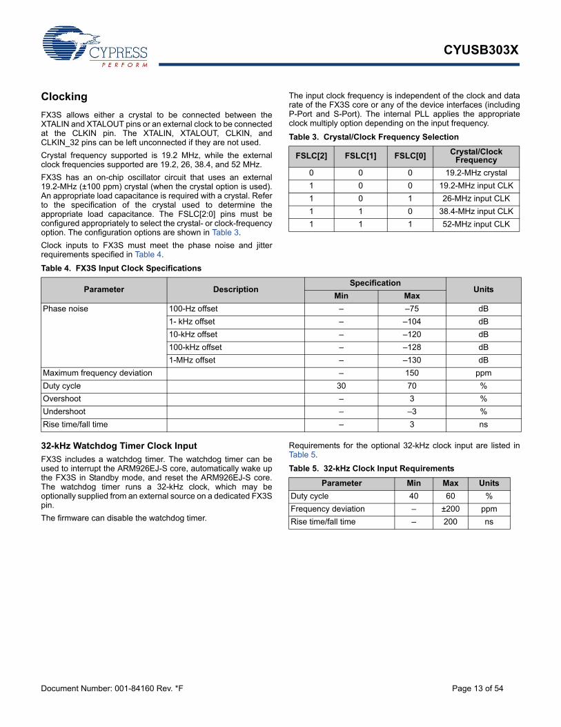
Clocking
FX3S allows either a crystal to be connected between theXTALIN and XTALOUT pins or an external clock to be connectedat the CLKIN pin. The XTALIN, XTALOUT, CLKIN, andCLKIN_32 pins can be left unconnected if they are not used.
Crystal frequency supported is 19.2 MHz, while the externalclock frequencies supported are 19.2, 26, 38.4, and 52 MHz.
FX3S has an on-chip oscillator circuit that uses an external19.2-MHz (±100 ppm) crystal (when the crystal option is used).An appropriate load capacitance is required with a crystal. Referto the specification of the crystal used to determine theappropriate load capacitance. The FSLC[2:0] pins must beconfigured appropriately to select the crystal- or clock-frequencyoption. The configuration options are shown in Table 3.
Clock inputs to FX3S must meet the phase noise and jitterrequirements specified in Table 4.
The input clock frequency is independent of the clock and datarate of the FX3S core or any of the device interfaces (includingP-Port and S-Port). The internal PLL applies the appropriateclock multiply option depending on the input frequency.
32-kHz Watchdog Timer Clock Input
FX3S includes a watchdog timer. The watchdog timer can beused to interrupt the ARM926EJ-S core, automatically wake upthe FX3S in Standby mode, and reset the ARM926EJ-S core.The watchdog timer runs a 32-kHz clock, which may beoptionally supplied from an external source on a dedicated FX3Spin.
The firmware can disable the watchdog timer.
Requirements for the optional 32-kHz clock input are listed inTable 5.
Table 3. Crystal/Clock Frequency Selection
FSLC[2] FSLC[1] FSLC[0] Crystal/ClockFrequency
0 0 0 19.2-MHz crystal
1 0 0 19.2-MHz input CLK
1 0 1 26-MHz input CLK
1 1 0 38.4-MHz input CLK
1 1 1 52-MHz input CLK
Table 4. FX3S Input Clock Specifications
Parameter DescriptionSpecification
UnitsMin Max
Phase noise 100-Hz offset – –75 dB
1- kHz offset – –104 dB
10-kHz offset – –120 dB
100-kHz offset – –128 dB
1-MHz offset – –130 dB
Maximum frequency deviation – 150 ppm
Duty cycle 30 70 %
Overshoot – 3 %
Undershoot – –3 %
Rise time/fall time – 3 ns
Table 5. 32-kHz Clock Input Requirements
Parameter Min Max Units
Duty cycle 40 60 %
Frequency deviation – ±200 ppm
Rise time/fall time – 200 ns

CYUSB303X
Document Number: 001-84160 Rev. *F Page 14 of 54
Power
FX3S has the following power supply domains:
IO_VDDQ: This is a group of independent supply domains fordigital I/Os. The voltage level on these supplies is 1.8 V to 3.3 V.FX3S provides six independent supply domains for digital I/Oslisted as follows (see Pin Description on page 18 for details oneach of the power domain signals): VIO1: GPIF II I/O VIO2: S0-Port Supply VIO3: S1-Port Supply VIO4: S1-Port and Low Speed Peripherals (UART/SPI/I2S)
Supply VIO5: I2C and JTAG (supports 1.2 V to 3.3 V) CVDDQ: Clock VDD: This is the supply voltage for the logic core. The nominal
supply-voltage level is 1.2 V. This supplies the core logiccircuits. The same supply must also be used for the following:• AVDD: This is the 1.2-V supply for the PLL, crystal
oscillator, and other core analog circuits• U3TXVDDQ/U3RXVDDQ: These are the 1.2-V supply
voltages for the USB 3.0 interface.
VBATT/VBUS: This is the 3.2-V to 6-V battery power supply forthe USB I/O and analog circuits. This supply powers the USBtransceiver through FX3S's internal voltage regulator. VBATTis internally regulated to 3.3 V.
Power Modes
FX3S supports the following power modes:
Normal mode: This is the full-functional operating mode. The internal CPU clock and the internal PLLs are enabled in this mode. Normal operating power consumption does not exceed the
sum of ICC Core max and ICC USB max (see the DC Specifications table for current consumption specifications).
The I/O power supplies VIO2, VIO3, VIO4, and VIO5 can be turned off when the corresponding interface is not in use. VIO1 cannot be turned off at any time if the GPIF II interface is used in the application.
Low-power modes (see Table 6): Suspend mode with USB 3.0 PHY enabled (L1) Suspend mode with USB 3.0 PHY disabled (L2) Standby mode (L3) Core power-down mode (L4)
Table 6. Entry and Exit Methods for Low-Power Modes
Low-Power Mode Characteristics Methods of Entry Methods of Exit
Suspend Mode with USB 3.0 PHY Enabled (L1)
The power consumption in this mode does not exceed ISB1
USB 3.0 PHY is enabled and is in U3 mode (one of the suspend modes defined by the USB 3.0 specification). This one block alone is operational with its internal clock while all other clocks are shut down
All I/Os maintain their previous state
Power supply for the wakeup source and core power must be retained. All other power domains can be turned on/off individually
The states of the configuration registers, buffer memory, and all internal RAM are maintained
All transactions must be completed before FX3S enters Suspend mode (state of outstanding transactions are not preserved)
The firmware resumes operation from where it was suspended (except when woken up by RESET# assertion) because the program counter does not reset
Firmware executing on ARM926EJ-S core can put FX3S into suspend mode. For example, on USB suspend condition, firmware may decide to put FX3S into suspend mode
External Processor, through the use of mailbox registers, can put FX3S into suspend mode
D+ transitioning to low or high
D- transitioning to low or high
Impedance change on OTG_ID pin
Resume condition on SSRX±
Detection of VBUS
Level detect on UART_CTS (programmable polarity)
GPIF II interface assertion of CTL[0]
Assertion of RESET#

CYUSB303X
Document Number: 001-84160 Rev. *F Page 15 of 54
Suspend Mode with USB 3.0 PHY Disabled (L2)
The power consumption in this mode does not exceed ISB2
USB 3.0 PHY is disabled and the USB interface is in suspend mode
The clocks are shut off. The PLLs are disabled
All I/Os maintain their previous state
USB interface maintains the previous state
Power supply for the wakeup source and core power must be retained. All other power domains can be turned on/off individually
The states of the configuration registers, buffer memory and all internal RAM are maintained
All transactions must be completed before FX3S enters Suspend mode (state of outstanding transactions are not preserved)
The firmware resumes operation from where it was suspended (except when woken up by RESET# assertion) because the program counter does not reset
Firmware executing on ARM926EJ-S core can put FX3S into suspend mode. For example, on USB suspend condition, firmware may decide to put FX3S into suspend mode
External Processor, through the use of mailbox registers can put FX3S into suspend mode
D+ transitioning to low or high
D- transitioning to low or high
Impedance change on OTG_ID pin
Resume condition on SSRX±
Detection of VBUS
Level detect on UART_CTS (programmable polarity)
GPIF II interface assertion of CTL[0]
Assertion of RESET#
Standby Mode (L3)
The power consumption in this mode does not exceed ISB3
All configuration register settings and program/data RAM contents are preserved. However, data in the buffers or other parts of the data path, if any, is not guaranteed. Therefore, the external processor should take care that the data needed is read before putting FX3S into this Standby Mode
The program counter is reset after waking up from Standby
GPIO pins maintain their configuration
Crystal oscillator is turned off
Internal PLL is turned off
USB transceiver is turned off
ARM926EJ-S core is powered down. Upon wakeup, the core re-starts and runs the program stored in the program/data RAM
Power supply for the wakeup source and core power must be retained. All other power domains can be turned on/off individually
Firmware executing on ARM926EJ-S core or external processor configures the appropriate register
Detection of VBUS
Level detect on UART_CTS (Programmable Polarity)
GPIF II interface assertion of CTL[0]
Assertion of RESET#
Table 6. Entry and Exit Methods for Low-Power Modes (continued)
Low-Power Mode Characteristics Methods of Entry Methods of Exit
CYUSB303X
Document Number: 001-84160 Rev. *F Page 16 of 54
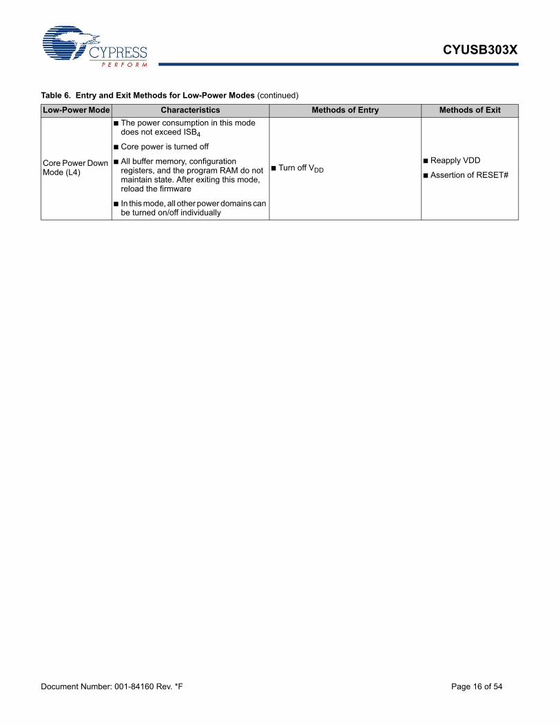
Core Power Down Mode (L4)
The power consumption in this mode does not exceed ISB4
Core power is turned off
All buffer memory, configuration registers, and the program RAM do not maintain state. After exiting this mode, reload the firmware
In this mode, all other power domains can be turned on/off individually
Turn off VDD
Reapply VDD
Assertion of RESET#
Table 6. Entry and Exit Methods for Low-Power Modes (continued)
Low-Power Mode Characteristics Methods of Entry Methods of Exit

CYUSB303X
Document Number: 001-84160 Rev. *F Page 17 of 54
Configuration Options
Configuration options are available for specific usage models.Contact Cypress Applications or Marketing for details.
Digital I/Os
FX3S has internal firmware-controlled pull-up or pull-downresistors on all digital I/O pins. An internal 50-k resistor pullsthe pins high, while an internal 10-k resistor pulls the pins lowto prevent them from floating. The I/O pins may have thefollowing states:
Tristated (High-Z)
Weak pull-up (via internal 50 k)
Pull-down (via internal 10 k)
Hold (I/O hold its value) when in low-power modes
The JTAG TDI, TMC, and TRST# signals have fixed 50-kinternal pull-ups, and the TCK signal has a fixed 10-kpull-down resistor.
All unused I/Os should be pulled high by using the internalpull-up resistors. All unused outputs should be left floating. AllI/Os can be driven at full-strength, three-quarter strength,half-strength, or quarter-strength. These drive strengths areconfigured separately for each interface.
GPIOs
EZ-USB enables a flexible pin configuration both on the GPIF IIand the serial peripheral interfaces. Any unused control pins(except CTL[15]) on the GPIF II interface can be used as GPIOs.Similarly, any unused pins on the serial peripheral interfaces maybe configured as GPIOs. See the Pin Description on page 18 forpin configuration options.
All GPIF II and GPIO pins support an external load of up to 16 pFfor every pin.
EMIFX3S meets EMI requirements outlined by FCC 15B (USA) andEN55022 (Europe) for consumer electronics. FX3S can toleratereasonable EMI, conducted by the aggressor, outlined by thesespecifications and continue to function as expected.
System-level ESD
FX3S has built-in ESD protection on the D+, D–, and GND pinson the USB interface. The ESD protection levels provided onthese ports are:
±2.2-KV human body model (HBM) based on JESD22-A114 Specification
±6-KV contact discharge and ±8-KV air gap discharge based on IEC61000-4-2 level 3A
± 8-KV Contact Discharge and ±15-KV Air Gap Discharge based on IEC61000-4-2 level 4C.
This protection ensures the device continues to function afterESD events up to the levels stated in this section.
The SSRX+, SSRX–, SSTX+, and SSTX– pins only have up to±2.2-KV HBM internal ESD protection.
Figure 11. FX3S Ball Map (Top View) 1 2 3 4 5 6 7 8 9 10 11
A U3VSSQ U3RXVDDQ SSRXM SSRXP SSTXP SSTXM AVDD VSS DP DM NC
B VIO4 FSLC[0] R_USB3 FSLC[1] U3TXVDDQ CVDDQ AVSS VSS VSS V DD TRST#
C GPIO[54] GPIO[55] VDD GPIO[57] RESET# XTALIN XTALOUT R_USB2 OTG_ID TDO VIO5
D GPIO[50] GPIO[51] GPIO[52] GPIO[53] GPIO[56] CLKIN_32 CLKIN VSS I2C_GPIO[58] I2C_GPIO[59] O[60]
E GPIO[47] VSS VIO3 GPIO[49] GPIO[48] FSLC[2] TDI TMS VDD VBATT V BUS
F VIO2 GPIO[45] GPIO[44] GPIO[41] GPIO[46] TCK GPIO[2] GPIO[5] GPIO[1] GPIO[0] VDD
G VSS GPIO[42] GPIO[43] GPIO[30] GPIO[25] GPIO[22] GPIO[21] GPIO[15] GPIO[4] GPIO[3] VSS
H VDD GPIO[39] GPIO[40] GPIO[31] GPIO[29] GPIO[26] GPIO[20] GPIO[24] GPIO[7] GPIO[6] VIO1
J GPIO[38] GPIO[36] GPIO[37] GPIO[34] GPIO[28] GPIO[16] GPIO[19] GPIO[14] GPIO[9] GPIO[8] VDD
K GPIO[35] GPIO[33] VSS VSS GPIO[27] GPIO[23] GPIO[18] GPIO[17] GPIO[13] GPIO[12] GPIO[10]
L VSS VSS VSS GPIO[32] VDD VSS VDD INT# VIO1 GPIO[11] VSS
CYUSB303X
Document Number: 001-84160 Rev. *F Page 18 of 54
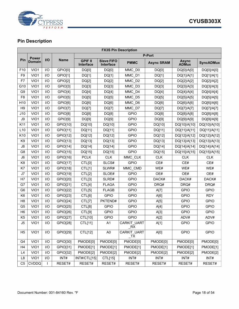
Pin Description
FX3S Pin Description
Pin Power Domain I/O Name
P-Port
GPIF II Interface
Slave FIFO Interface PMMC Async SRAM Async
ADMux SyncADMux
F10 VIO1 I/O GPIO[0] DQ[0] DQ[0] MMC_D0 DQ[0] DQ[0]/A[0] DQ[0]/A[0]
F9 VIO1 I/O GPIO[1] DQ[1] DQ[1] MMC_D1 DQ[1] DQ[1]/A[1] DQ[1]/A[1]
F7 VIO1 I/O GPIO[2] DQ[2] DQ[2] MMC_D2 DQ[2] DQ[2]/A[2] DQ[2]/A[2]
G10 VIO1 I/O GPIO[3] DQ[3] DQ[3] MMC_D3 DQ[3] DQ[3]/A[3] DQ[3]/A[3]
G9 VIO1 I/O GPIO[4] DQ[4] DQ[4] MMC_D4 DQ[4] DQ[4]/A[4] DQ[4]/A[4]
F8 VIO1 I/O GPIO[5] DQ[5] DQ[5] MMC_D5 DQ[5] DQ[5]/A[5] DQ[5]/A[5]
H10 VIO1 I/O GPIO[6] DQ[6] DQ[6] MMC_D6 DQ[6] DQ[6]/A[6] DQ[6]/A[6]
H9 VIO1 I/O GPIO[7] DQ[7] DQ[7] MMC_D7 DQ[7] DQ[7]/A[7] DQ[7]/A[7]
J10 VIO1 I/O GPIO[8] DQ[8] DQ[8] GPIO DQ[8] DQ[8]/A[8] DQ[8]/A[8]
J9 VIO1 I/O GPIO[9] DQ[9] DQ[9] GPIO DQ[9] DQ[9]/A[9] DQ[9]/A[9]
K11 VIO1 I/O GPIO[10] DQ[10] DQ[10] GPIO DQ[10] DQ[10]/A[10] DQ[10]/A[10]
L10 VIO1 I/O GPIO[11] DQ[11] DQ[11] GPIO DQ[11] DQ[11]/A[11] DQ[11]/A[11]
K10 VIO1 I/O GPIO[12] DQ[12] DQ[12] GPIO DQ[12] DQ[12]/A[12] DQ[12]/A[12]
K9 VIO1 I/O GPIO[13] DQ[13] DQ[13] GPIO DQ[13] DQ[13]/A[13] DQ[13]/A[13]
J8 VIO1 I/O GPIO[14] DQ[14] DQ[14] GPIO DQ[14] DQ[14]/A[14] DQ[14]/A[14]
G8 VIO1 I/O GPIO[15] DQ[15] DQ[15] GPIO DQ[15] DQ[15]/A[15] DQ[15]/A[15]
J6 VIO1 I/O GPIO[16] PCLK CLK MMC_CLK CLK CLK CLK
K8 VIO1 I/O GPIO[17] CTL[0] SLCS# GPIO CE# CE# CE#
K7 VIO1 I/O GPIO[18] CTL[1] SLWR# MMC_CMD WE# WE# WE#
J7 VIO1 I/O GPIO[19] CTL[2] SLOE# GPIO OE# OE# OE#
H7 VIO1 I/O GPIO[20] CTL[3] SLRD# GPIO DACK# DACK# DACK#
G7 VIO1 I/O GPIO[21] CTL[4] FLAGA GPIO DRQ# DRQ# DRQ#
G6 VIO1 I/O GPIO[22] CTL[5] FLAGB GPIO A[7] GPIO GPIO
K6 VIO1 I/O GPIO[23] CTL[6] GPIO GPIO A[6] GPIO RDY
H8 VIO1 I/O GPIO[24] CTL[7] PKTEND# GPIO A[5] GPIO GPIO
G5 VIO1 I/O GPIO[25] CTL[8] GPIO GPIO A[4] GPIO GPIO
H6 VIO1 I/O GPIO[26] CTL[9] GPIO GPIO A[3] GPIO GPIO
K5 VIO1 I/O GPIO[27] CTL[10] GPIO GPIO A[2] ADV# ADV#
J5 VIO1 I/O GPIO[28] CTL[11] A1 CARKIT_UART_RX
A[1] GPIO GPIO
H5 VIO1 I/O GPIO[29] CTL[12] A0 CARKIT_UART_TX
A[0] GPIO GPIO
G4 VIO1 I/O GPIO[30] PMODE[0] PMODE[0] PMODE[0] PMODE[0] PMODE[0] PMODE[0]
H4 VIO1 I/O GPIO[31] PMODE[1] PMODE[1] PMODE[1] PMODE[1] PMODE[1] PMODE[1]
L4 VIO1 I/O GPIO[32] PMODE[2] PMODE[2] PMODE[2] PMODE[2] PMODE[2] PMODE[2]
L8 VIO1 I/O INT# INT#/CTL[15] CTL[15] INT# INT# INT# INT#
C5 CVDDQ I RESET# RESET# RESET# RESET# RESET# RESET# RESET#
CYUSB303X
Document Number: 001-84160 Rev. *F Page 19 of 54
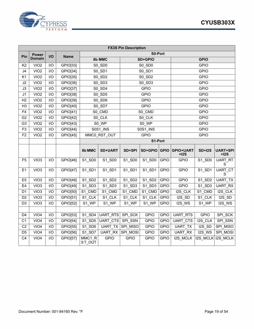
FX3S Pin Description
Pin Power Domain I/O Name
S0-Port
8b MMC SD+GPIO GPIO
K2 VIO2 I/O GPIO[33] S0_SD0 S0_SD0 GPIO
J4 VIO2 I/O GPIO[34] S0_SD1 S0_SD1 GPIO
K1 VIO2 I/O GPIO[35] S0_SD2 S0_SD2 GPIO
J2 VIO2 I/O GPIO[36] S0_SD3 S0_SD3 GPIO
J3 VIO2 I/O GPIO[37] S0_SD4 GPIO GPIO
J1 VIO2 I/O GPIO[38] S0_SD5 GPIO GPIO
H2 VIO2 I/O GPIO[39] S0_SD6 GPIO GPIO
H3 VIO2 I/O GPIO[40] S0_SD7 GPIO GPIO
F4 VIO2 I/O GPIO[41] S0_CMD S0_CMD GPIO
G2 VIO2 I/O GPIO[42] S0_CLK S0_CLK GPIO
G3 VIO2 I/O GPIO[43] S0_WP S0_WP GPIO
F3 VIO2 I/O GPIO[44] S0S1_INS S0S1_INS GPIO
F2 VIO2 I/O GPIO[45] MMC0_RST_OUT GPIO GPIO
S1-Port
8b MMC SD+UART SD+SPI SD+GPIO GPIO
GPIO+UART+I2S
SD+I2S
UART+SPI+I2S
F5 VIO3 I/O GPIO[46] S1_SD0 S1_SD0 S1_SD0 S1_SD0 GPIO GPIO S1_SD0 UART_RTS
E1 VIO3 I/O GPIO[47] S1_SD1 S1_SD1 S1_SD1 S1_SD1 GPIO GPIO S1_SD1 UART_CTS
E5 VIO3 I/O GPIO[48] S1_SD2 S1_SD2 S1_SD2 S1_SD2 GPIO GPIO S1_SD2 UART_TX
E4 VIO3 I/O GPIO[49] S1_SD3 S1_SD3 S1_SD3 S1_SD3 GPIO GPIO S1_SD3 UART_RX
D1 VIO3 I/O GPIO[50] S1_CMD S1_CMD S1_CMD S1_CMD GPIO I2S_CLK S1_CMD I2S_CLK
D2 VIO3 I/O GPIO[51] S1_CLK S1_CLK S1_CLK S1_CLK GPIO I2S_SD S1_CLK I2S_SD
D3 VIO3 I/O GPIO[52] S1_WP S1_WP S1_WP S1_WP GPIO I2S_WS S1_WP I2S_WS
D4 VIO4 I/O GPIO[53] S1_SD4 UART_RTS SPI_SCK GPIO GPIO UART_RTS GPIO SPI_SCK
C1 VIO4 I/O GPIO[54] S1_SD5 UART_CTS SPI_SSN GPIO GPIO UART_CTS I2S_CLK SPI_SSN
C2 VIO4 I/O GPIO[55] S1_SD6 UART_TX SPI_MISO GPIO GPIO UART_TX I2S_SD SPI_MISO
D5 VIO4 I/O GPIO[56] S1_SD7 UART_RX SPI_MOSI GPIO GPIO UART_RX I2S_WS SPI_MOSI
C4 VIO4 I/O GPIO[57] MMC1_RS T_OUT
GPIO GPIO GPIO GPIO I2S_MCLK I2S_MCLK I2S_MCLK
CYUSB303X
Document Number: 001-84160 Rev. *F Page 20 of 54
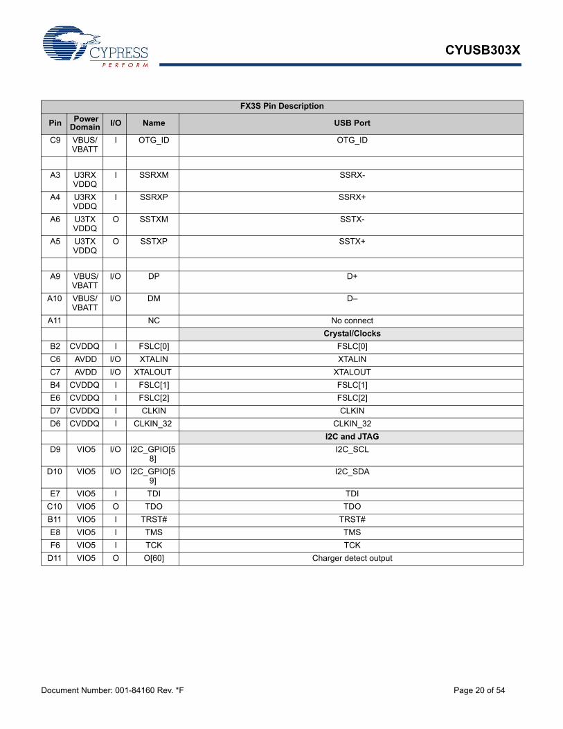
FX3S Pin Description
Pin Power Domain I/O Name USB Port
C9 VBUS/VBATT
I OTG_ID OTG_ID
A3 U3RXVDDQ
I SSRXM SSRX-
A4 U3RXVDDQ
I SSRXP SSRX+
A6 U3TXVDDQ
O SSTXM SSTX-
A5 U3TXVDDQ
O SSTXP SSTX+
A9 VBUS/VBATT
I/O DP D+
A10 VBUS/VBATT
I/O DM D–
A11 NC No connect
Crystal/Clocks
B2 CVDDQ I FSLC[0] FSLC[0]
C6 AVDD I/O XTALIN XTALIN
C7 AVDD I/O XTALOUT XTALOUT
B4 CVDDQ I FSLC[1] FSLC[1]
E6 CVDDQ I FSLC[2] FSLC[2]
D7 CVDDQ I CLKIN CLKIN
D6 CVDDQ I CLKIN_32 CLKIN_32
I2C and JTAG
D9 VIO5 I/O I2C_GPIO[58]
I2C_SCL
D10 VIO5 I/O I2C_GPIO[59]
I2C_SDA
E7 VIO5 I TDI TDI
C10 VIO5 O TDO TDO
B11 VIO5 I TRST# TRST#
E8 VIO5 I TMS TMS
F6 VIO5 I TCK TCK
D11 VIO5 O O[60] Charger detect output

CYUSB303X
Document Number: 001-84160 Rev. *F Page 21 of 54
FX3S Pin Description
Pin Power Domain I/O Name Power
E10 PWR VBATT
B10 PWR VDD
A1 PWR U3VSSQ
E11 PWR VBUS
D8 PWR VSS
H11 PWR VIO1
E2 PWR VSS
L9 PWR VIO1
G1 PWR VSS
F1 PWR VIO2
G11 PWR VSS
E3 PWR VIO3
L1 PWR VSS
B1 PWR VIO4
L6 PWR VSS
B6 PWR CVDDQ
B5 PWR U3TXVDDQ
A2 PWR U3RXVDDQ
C11 PWR VIO5
L11 PWR VSS
A7 PWR AVDD
B7 PWR AVSS
C3 PWR VDD
B8 PWR VSS
E9 PWR VDD
B9 PWR VSS
F11 PWR VDD
H1 PWR VDD
L7 PWR VDD
J11 PWR VDD
L5 PWR VDD
K4 PWR VSS
L3 PWR VSS
K3 PWR VSS
L2 PWR VSS
A8 PWR VSS
Precision Resistors
C8 VBUS/VBATT
I/O R_usb2 Precision resistor for USB 2.0 (Connect a 6.04 kΩ ±1% resistor between this pin and GND)
B3 U3TXVDDQ
I/O R_usb3 Precision resistor for USB 3.0 (Connect a 200 Ω ±1% resistor between this pin and GND)

CYUSB303X
Document Number: 001-84160 Rev. *F Page 22 of 54
Absolute Maximum Ratings
Exceeding maximum ratings may shorten the useful life of thedevice.
Storage temperature .............................. ...... –65 °C to +150 °C
Ambient temperature with power supplied (Industrial) ...................... ...... –40 °C to +85 °C
Supply voltage to ground potential VDD, AVDDQ ......................................................................1.25 V
VIO1,VIO2, VIO3, VIO4, VIO5 ............................................. ...3.6 V
U3TXVDDQ, U3RXVDDQ .............................................. .....1.25 V
DC input voltage to any input pin ................................VCC + 0.3
DC voltage applied to outputs in high Z state ................................................VCC + 0.3
(VCC is the corresponding I/O voltage)
Static discharge voltage ESD protection levels:
± 2.2-KV HBM based on JESD22-A114
Additional ESD protection levels on D+, D–, and GND pins, and serial peripheral pins
± 6-KV contact discharge, ± 8-KV air gap discharge based on IEC61000-4-2 level 3A, ± 8-KV contact discharge, and ± 15-KV air gap discharge based on IEC61000-4-2 level 4C
Latch-up current .........................................................> 200 mA
Maximum output short-circuit current for all I/O configurations. (Vout = 0 V) ......................... –100 mA
Operating Conditions
TA (ambient temperature under bias)
Industrial ........................................................ –40 °C to +85 °C
VDD, AVDDQ, U3TXVDDQ, U3RXVDDQ
Supply voltage ..................................................1.15 V to 1.25 V
VBATT supply voltage ...............................................3.2 V to 6 V
VIO1, VIO2, VIO3, VIO4, CVDDQ
Supply voltage ......................................................1.7 V to 3.6 V
VIO5 supply voltage ............................................ 1.15 V to 3.6 V
DC Specifications
Parameter Description Min Max Units Notes
VDD Core voltage supply 1.15 1.25 V 1.2-V typical
AVDD Analog voltage supply 1.15 1.25 V 1.2-V typical
VIO1 GPIF II I/O power supply domain 1.7 3.6 V 1.8-, 2.5-, and 3.3-V typical
VIO2 S0-Port power supply domain 1.7 3.6 V 1.8-, 2.5-, and 3.3-V typical
VIO3 S1-Port power supply domain 1.7 3.6 V 1.8-, 2.5-, and 3.3-V typical
VIO4S1-Port and UART/SPI/I2S power supply domain 1.7 3.6 V 1.8-, 2.5-, and 3.3-V typical
VBATT USB voltage supply 3.2 6 V 3.7-V typical
VBUS USB voltage supply 4.0 6 V 5-V typical
U3TXVDDQ USB 3.0 1.2-V supply 1.15 1.25 V1.2-V typical. A 22-µF bypass capacitor is required on this power supply.
U3RXVDDQ USB 3.0 1.2-V supply 1.15 1.25 V1.2-V typical. A 22-µF bypass capacitor is required on this power supply.
CVDDQ Clock voltage supply 1.7 3.6 V 1.8-, 3.3-V typical
VIO5 I2C and JTAG voltage supply 1.15 3.6 V 1.2-, 1.8-, 2.5-, and 3.3-V typical
VIH1 Input HIGH voltage 1 0.625 × VCC VCC + 0.3 VFor 2.0 V VCC 3.6 V (except USB port).VCC is the corresponding I/O voltage supply.
VIH2 Input HIGH voltage 2 VCC – 0.4 VCC + 0.3 VFor 1.7 V VCC 2.0 V (except USB port).VCC is the corresponding I/O voltage supply.

CYUSB303X
Document Number: 001-84160 Rev. *F Page 23 of 54
VIL Input LOW voltage –0.3 0.25 × VCC V VCC is the corresponding I/O voltage supply.
VOH Output HIGH voltage 0.9 × VCC – VIOH (max) = –100 µA tested at quarter drive strength. VCC is the corresponding I/O voltage supply.
VOL Output LOW voltage – 0.1 × VCC VIOL (min) = +100 µA tested at quarter drive strength. VCC is the corresponding I/O voltage supply.
IIXInput leakage current for all pins except SSTXP/SSXM/SSRXP/SSRXM
–1 1 µA
All I/O signals held at VDDQ(For I/Os with a pull-up or pull-down resistor connected, the leakage current increases by VDDQ/Rpu or VDDQ/RPD
IOZ
Output High-Z leakage current for all pins except SSTXP/ SSXM/ SSRXP/SSRXM
–1 1 µA All I/O signals held at VDDQ
ICC Core Core and analog voltage operating current
– 200 mA Total current through AVDD, VDD
ICC USB USB voltage supply operating current
– 60 mA
ISB1
Total suspend current during suspend mode with USB 3.0 PHY enabled (L1)
– – mA
Core current: 1.5 mAI/O current: 20 µAUSB current: 2 mAFor typical PVT (typical silicon, all power supplies at their respective nominal levels at 25 °C.)
ISB2
Total suspend current during suspend mode with USB 3.0 PHY disabled (L2)
– – mA
Core current: 250 µAI/O current: 20 µAUSB current: 1.2 mAFor typical PVT (Typical silicon, all power supplies at their respective nominal levels at 25 °C.)
ISB3Total standby current during standby mode (L3)
– – µA
Core current: 60 µAI/O current: 20 µAUSB current: 40 µAFor typical PVT (typical silicon, all power supplies at their respective nominal levels at 25 °C.)
ISB4Total standby current during core power-down mode (L4)
– – µA
Core current: 0 µAI/O current: 20 µAUSB current: 40 µAFor typical PVT (typical silicon, all power supplies at their respective nominal levels at 25 °C.)
VRAMPVoltage ramp rate on core and I/O supplies
0.2 50 V/ms Voltage ramp must be monotonic
VNNoise level permitted on VDD and I/O supplies
– 100 mV Max p-p noise level permitted on all supplies except AVDD
VN_AVDDNoise level permitted on AVDD supply
– 20 mV Max p-p noise level permitted on AVDD
DC Specifications (continued)
Parameter Description Min Max Units Notes

CYUSB303X
Document Number: 001-84160 Rev. *F Page 24 of 54
AC Timing ParametersGPIF II Timing
Figure 12. GPIF II Timing in Synchronous Mode
-
CTL ( OUT)
CTL( IN)
tS tH
tDHtDS
tCLK
CLK
tCTLO
tCOE
Data ( IN)Data 1 ( OUT)
tHZ
tLZ tDOH
tCOH
tCLKH tCLKL
tLZ
Data 2 ( OUT)
tCO
tDOH
DQ[15:0]
Table 7. GPIF II Timing Parameters in Synchronous Mode [3]
Parameter Description Min Max Units
Frequency Interface clock frequency – 100 MHz
tCLK Interface clock period 10 – ns
tCLKH Clock high time 4 – ns
tCLKL Clock low time 4 – ns
tS CTL input to clock setup time (Sync speed = 1) 2 – ns
tH CTL input to clock hold time (Sync speed = 1) 0.5 – ns
tDS Data in to clock setup time (Sync speed = 1) 2 – ns
tDH Data in to clock hold time (Sync speed = 1) 0.5 – ns
tCO Clock to data out propagation delay when DQ bus is already in output direction (Sync speed = 1) – 8 ns
tCOEClock to data out propagation delay when DQ lines change to output from tristate and valid data is available on the DQ bus (Sync speed = 1)
- 9
tCTLO Clock to CTL out propagation delay (Sync speed = 1) – 8 ns
tDOH Clock to data out hold 2 – ns
tCOH Clock to CTL out hold 0 – ns
tHZ Clock to high-Z – 8 ns
tLZ Clock to low-Z (Sync speed = 1) 0 – ns
tS_ss0 CTL input/data input to clock setup time (Sync speed = 0) 5 – ns
tH_ss0 CTL input/data input to clock hold time (Sync speed = 0) 2.5 – ns
tCO_ss0 Clock to data out / CTL out propagation delay (sync speed = 0) – 15 ns
tLZ_ss0 Clock to low-Z (sync speed = 0) 2 – ns
Note3. All parameters guaranteed by design and validated through characterization.

CYUSB303X
Document Number: 001-84160 Rev. *F Page 25 of 54
Figure 13. GPIF II Timing in Asynchronous Mode
Figure 14. GPIF II Timing in Asynchronous DDR Mode
DATA/ ADDR
CTL#(I/P , ALE/ DLE)
tCHZ
tCTLalpha
tCTLbeta
tDH/tAH
tCTLdeassert_DQlatch
tCTLdeassert
DATA IN
tCTLassert_DQlatch
tCHZ/tOEHZtCLZ/ tOELZ
tDS/ tAS
DATA OUTDATA OUT
CTL#(I/P, non ALE/ DLE
ALPHAO/P
BETAO/P
tCTL#(O/P)
tCTLassert tCTLdeassert1 1
1. n is an integer >= 0
tAA/tDO
tCTLassert
DATA/ADDR
CTL#I/P (non DLE/ALE)
tDST tDHT
tCTLassert_DQassert
tCTLdeassert_DQassert
DATA IN
CTL#(I/P)
tDS
tCTLassert_DQlatchDDR
tCTLdeassert_DqlatchDDR
tDH
tDS tDH

CYUSB303X
Document Number: 001-84160 Rev. *F Page 26 of 54
Table 8. GPIF II Timing in Asynchronous Mode [4]
Note The following parameters assume one state transition.
Parameter Description Min Max Units
tDS Data In to DLE setup time. Valid in DDR async mode. 2.3 – ns
tDH Data In to DLE hold time. Valid in DDR async mode. 2 – ns
tAS Address In to ALE setup time 2.3 – ns
tAH Address In to ALE hold time 2 – ns
tCTLassert CTL I/O asserted width for CTRL inputs without DQ input association and for outputs.
7 – ns
tCTLdeassertCTL I/O deasserted width for CTRL inputs without DQ input association and for outputs. 7 – ns
tCTLassert_DQassertCTL asserted pulse width for CTL inputs that signify DQ inputs valid at the asserting edge but do not employ in-built latches (ALE/DLE) for those DQ inputs.
20 – ns
tCTLdeassert_DQassertCTL deasserted pulse width for CTL inputs that signify DQ input valid at the asserting edge but do not employ in-built latches (ALE/DLE) for those DQ inputs.
7 – ns
tCTLassert_DQdeassertCTL asserted pulse width for CTL inputs that signify DQ inputs valid at the deasserting edge but do not employ in-built latches (ALE/DLE) for those DQ inputs.
7 – ns
tCTLdeassert_DQdeassertCTL deasserted pulse width for CTL inputs that signify DQ inputs valid at the deasserting edge but do not employ in-built latches (ALE/DLE) for those DQ inputs.
20 – ns
tCTLassert_DQlatch
CTL asserted pulse width for CTL inputs that employ in-built latches (ALE/DLE) to latch the DQ inputs. In this non-DDR case, in-built latches are always close at the deasserting edge.
7 – ns
tCTLdeassert_DQlatch
CTL deasserted pulse width for CTL inputs that employ in-built latches (ALE/DLE) to latch the DQ inputs. In this non-DDR case, in-built latches always close at the deasserting edge.
10 – ns
tCTLassert_DQlatchDDR CTL asserted pulse width for CTL inputs that employ in-built latches (DLE) to latch the DQ inputs in DDR mode.
10 – ns
tCTLdeassert_DQlatchDDRCTL deasserted pulse width for CTL inputs that employ in-built latches (DLE) to latch the DQ inputs in DDR mode. 10 – ns
tAADQ/CTL input to DQ output time when DQ change or CTL change needs to be detected and affects internal updates of input and output DQ lines.
– 30 ns
tDO CTL to data out when the CTL change merely enables the output flop update whose data was already established. – 25 ns
tOELZ CTL designated as OE to low-Z. Time when external devices should stop driving data.
0 – ns
tOEHZ CTL designated as OE to high-Z 8 8 ns
tCLZ CTL (non-OE) to low-Z. Time when external devices should stop driving data.
0 – ns
tCHZ CTL (non-OE) to high-Z 30 30 ns
tCTLalpha CTL to alpha change at output – 25 ns
tCTLbeta CTL to beta change at output – 30 ns
tDST Addr/data setup when DLE/ALE not used 2 – ns
tDHT Addr/data hold when DLE/ALE not used 20 – ns
Note4. All parameters guaranteed by design and validated through characterization.

CYUSB303X
Document Number: 001-84160 Rev. *F Page 27 of 54
Asynchronous SRAM Timing
Figure 15. Non-multiplexed Asynchronous SRAM Read Timing
tRC
tOE
tOLZ
tOHH
ADDRESS
CE#
OE#
DATA OUTHIGH
IMPEDANCE
OE# Controlled Timing
Socket Read – Address Transition Controlled Timing (OE# is asserted)
HIGH IMPEDANCE
DATA VALID
DATA VALID
HIGH IMPEDANCE
tOHC
tAOS
tOEZ
WE# (HIGH)
DATA OUT
tAA
tOH
A[0]
HIGH IMPEDANCE
DATA VALID DATA VALID DATA VALID
OE# tOE
tAH
CYUSB303X
Document Number: 001-84160 Rev. *F Page 28 of 54
Figure 16. Non-multiplexed Asynchronous SRAM Write Timing (WE# and CE# Controlled)
Figure 17. Non-multiplexed Asynchronous SRAM Write Timing (WE# Controlled, OE# LOW)
Write Cycle 2 CE# Controlled, OE# High During Write
tWC
tCW
tAW
tAS
tAH
tDS tDH
tWHZ
VALID DATA
ADDRESS
DATA I/O
tWP
CE#
WE#
OE#
Write Cycle 1 WE# Controlled, OE# High During Write
tWPH
VALID DATA
tWC
tCW
tAW
tAS
tAH
tDS tDH
tWHZ
VALID DATA
ADDRESS
DATA I/O
tWP
CE#
WE#
OE#
tCPH
VALID DATA
tWC
tCW
tAW
tAS
tAH
tDS tDH
VALID DATA
CE#
WE#
DATA I/O
tWP
tOWtWHZ
Write Cycle 3 WE# Controlled. OE# Low
Note: tWP must be adjusted such that tWP > tWHZ + tDS

CYUSB303X
Document Number: 001-84160 Rev. *F Page 29 of 54
Table 9. Asynchronous SRAM Timing Parameters[5]
Parameter Description Min Max Units
– SRAM interface bandwidth – 61.5 MBps
tRC Read cycle time 32.5 – ns
tAA Address to data valid – 30 ns
tAOS Address to OE# LOW setup time 7 – ns
tOH Data output hold from address change 3 – ns
tOHH OE# HIGH hold time 7.5 – ns
tOHC OE# HIGH to CE# HIGH 2 – ns
tOE OE# LOW to data valid – 25 ns
tOLZ OE# LOW to LOW-Z 0 – ns
tWC Write cycle time 30 – ns
tCW CE# LOW to write end 30 – ns
tAW Address valid to write end 30 – ns
tAS Address setup to write start 7 – ns
tAH Address hold time from CE# or WE# 2 – ns
tWP WE# pulse width 20 – ns
tWPH WE# HIGH time 10 – ns
tCPH CE# HIGH time 10 – ns
tDS Data setup to write end 7 – ns
tDH Data hold to write end 2 – ns
tWHZ Write to DQ HIGH-Z output – 22.5 ns
tOEZ OE# HIGH to DQ HIGH-Z output – 22.5 ns
tOW End of write to LOW-Z output 0 – ns
Note5. All parameters guaranteed by design and validated through characterization.

CYUSB303X
Document Number: 001-84160 Rev. *F Page 30 of 54
ADMux Timing for Asynchronous Access
Figure 18. ADMux Asynchronous Random Read
Figure 19. ADMux Asynchronous Random Write
Valid AddressA[0:7]/DQ[0:15]
ADV#
OE#
CE#
Valid Data
tVP
tAVS tAVH
tAVOE
tCO
tRC
tHZ
tHZ
tOE
tOLZ
tCEAV
Note: 1. Multiple read cycles can be executed while keeping CE# low.2. Read operation ends with either de-assertion of either OE# or CE#, whichever comes earlier.
Valid Addr
tACC
WE# (HIGH)
tCPH
Address ValidA[0:7]/DQ[0:15]
ADV#
WE#
CE#
Data Valid
tAVWEtWP
tDS tDH
tVP
tAVS tAVH
tCW
Note: 1. Multiple write cycles can be executed while keeping CE# low. 2. Write operation ends with de-assertion of either WE# or CE#, whichever comes earlier.
tCPH
tWC
Valid Addr
tAW
tVPH
tCEAV
tWPH

CYUSB303X
Document Number: 001-84160 Rev. *F Page 31 of 54
Table 10. Asynchronous ADMux Timing Parameters [6]
Parameter Description Min Max Units Notes
ADMux Asynchronous READ Access Timing Parameters
tRC Read cycle time (address valid to address valid)
54.5 – ns This parameter is dependent on when the P-port processors deasserts OE#
tACC Address valid to data valid – 32 ns –
tCO CE# assert to data valid – 34.5 ns –
tAVOE ADV# deassert to OE# assert 2 – ns –
tOLZ OE# assert to data LOW-Z 0 – ns –
tOE OE# assert to data valid – 25 ns –
tHZ Read cycle end to data HIGH-Z – 22.5 ns –
ADMux Asynchronous WRITE Access Timing Parameters
tWCWrite cycle time (Address Valid to Address Valid) – 52.5 ns –
tAW Address valid to write end 30 – ns –
tCW CE# assert to write end 30 – ns –
tAVWE ADV# deassert to WE# assert 2 – ns –
tWP WE# LOW pulse width 20 – ns –
tWPH WE# HIGH pulse width 10 – ns –
tDS Data valid setup to WE# deassert 18 – ns –
tDH Data valid hold from WE# deassert 2 – ns –
ADMux Asynchronous Common READ/WRITE Access Timing Parameters
tAVS Address valid setup to ADV# deassert 5 – ns –
tAVH Address valid hold from ADV# deassert 2 – ns –
tVP ADV# LOW pulse width 7.5 – ns –
tCPH CE# HIGH pulse width 10 – ns –
tVPH ADV# HIGH pulse width 15 – ns –
tCEAV CE# assert to ADV# assert 0 – ns –
Note6. All parameters guaranteed by design and validated through characterization.

CYUSB303X
Document Number: 001-84160 Rev. *F Page 32 of 54
Synchronous ADMux Timing
Figure 20. Synchronous ADMux Interface – Read Cycle Timing
Figure 21. Synchronous ADMux Interface – Write Cycle Timing
A[0:7]/DQ[0:15]
ADV#
CE#
OE#
RDY
tAVOE
tS
Valid Address
tS
tH
tS tH
tCO
tOHZ
tCLKH tCLKL
CLK
tCH
tKW tKW
tOLZ
tCLK2- cycle latency from OE# to DATA
WE# (HIGH)
Valid Data
Note:
1) External P-Port processor and FX3S operate on the same clock edge2) External processor sees RDY assert 2 cycles after OE # asserts andand sees RDY deassert a cycle after the data appears on the output3) Valid output data appears 2 cycle after OE # asserted. The data is held until OE # deasserts4) Two cycle latency is shown for 0-100 MHz operation. Latency can be reduced by 1 cycle for operations at less than 50 MHz (this 1 cycle latency is not supported by the bootloader)
A[0:7]/DQ[0:15]
ADV#
CE#
WE#
RDY
tAVWE
tS
Valid Address
tS
Valid Data
tH
tS tH
tDHtDS
tCLK
CLK
tKW
Note:
1) External P-Port processor and FX3S operate on the same clock edge2) External processor sees RDY assert 2 cycles after WE # asserts and deassert 3 cycles after the edge sampling the data.3) Two cycle latency is shown for 0-100 MHz operation. Latency can be reduced by 1 cycle for operations at less than 50 MHz (this 1 cycle latency is not supported by the bootloader)
tS tH
tKW
2-cycle latency betweenWE# and data being latched
2-cycle latency between this clk edge and RDY deassertion seen by the host

CYUSB303X
Document Number: 001-84160 Rev. *F Page 33 of 54
Figure 22. Synchronous ADMux Interface – Burst Read Timing
Figure 23. Sync ADMux Interface – Burst Write Timing
A[0:7]/DQ[0:15]
ADV#
CE#
OE#
RDY
tAVOE
tS
Valid Address
tS
D0 D1
tH
tS tH
tCH
tCO
D2
tCLKH tCLKL
tCLK
CLK
D3
2-cycle latency from OE# to Data
tKW
tKW
tHZ
tOLZ
Note:
1) External P-Port processor and FX3S work operate on the same clock edge2) External processor sees RDY assert 2 cycles after OE # asserts andand sees RDY deassert a cycle after the last burst data appears on the output3) Valid output data appears 2 cycle after OE # asserted. The last burst data is held until OE # deasserts4) Burst size of 4 is shown. Transfer size for the operation must be a multiple of burst size. Burst size is usually power of 2. RDY will not deassert in the middle of the burst. 5) External processor cannot deassert OE in the middle of a burst. If it does so, any bytes remaining in the burst packet could get lost.6) Two cycle latency is shown for 0-100 MHz operation. Latency can be reduced by 1 cycle for operations at less than 50 MHz (this 1 cycle latency is not supported by the bootloader)
A[0:7]/DQ[0:15]
ADV#
CE#
WE#
tAVWE
tS
Valid Address
tS
D1
tH
tS tH
tDHtDS
D3
tDH
tCLKH tCLKL
tCLK
CLK
D0
RDYtKW
D2
2-cycle latency betweenWE# and data being latched
tKW
2-cycle latency between this clk edge and RDY deassertion seen by the host
Note:
1) External P-Port processor and FX3S operate on the same clock edge2) External processor sees RDY assert 2 cycles after WE # asserts and deasserts 3 cycles after the edge sampling the last burst data.3) Transfer size for the operation must be a multiple of burst size. Burst size is usually power of 2. RDY will not deassert in the middle of the burst. Burst size of 4 is shown 4) External processor cannot deassert WE in the middle of a burst. If it does so, any bytes remaining in the burst packet could get lost. 5)Two cycle latency is shown for 0-100 MHz operation. Latency can be reduced by 1 cycle for operations at less than 50 MHz (this 1 cycle latency is not supported by the bootloader)

CYUSB303X
Document Number: 001-84160 Rev. *F Page 34 of 54
Table 11. Synchronous ADMux Timing Parameters[7]
Parameter Description Min Max Unit
FREQ Interface clock frequency – 100 MHz
tCLK Clock period 10 – ns
tCLKH Clock HIGH time 4 – ns
tCLKL Clock LOW time 4 – ns
tS CE#/WE#/DQ setup time 2 – ns
tH CE#/WE#/DQ hold time 0.5 – ns
tCH Clock to data output hold time 0 – ns
tDS Data input setup time 2 – ns
tDH Clock to data input hold 0.5 – ns
tAVDOE ADV# HIGH to OE# LOW 0 – ns
tAVDWE ADV# HIGH to WE# LOW 0 – ns
tHZ CE# HIGH to Data HIGH-Z – 8 ns
tOHZ OE# HIGH to Data HIGH-Z – 8 ns
tOLZ OE# LOW to Data LOW-Z 0 – ns
tKW Clock to RDY valid – 8 ns
Note7. All parameters guaranteed by design and validated through characterization.

CYUSB303X
Document Number: 001-84160 Rev. *F Page 35 of 54
Slave FIFO Interface
Synchronous Slave FIFO Sequence Description
FIFO address is stable and SLCS is asserted
FLAG indicates FIFO not empty status
SLOE is asserted. SLOE is an output-enable only, whose sole function is to drive the data bus.
SLRD is asserted
The FIFO pointer is updated on the rising edge of the PCLK,while the SLRD is asserted. This starts the propagation of datafrom the newly addressed location to the data bus. After apropagation delay of tco (measured from the rising edge ofPCLK), the new data value is present. N is the first data valueread from the FIFO. To have data on the FIFO data bus, SLOEmust also be asserted.
The same sequence of events is shown for a burst read.
FLAG Usage:
The FLAG signals are monitored for flow control by the externalprocessor. FLAG signals are outputs from FX3 that may beconfigured to show empty, full, or partial status for a dedicatedthread or the current thread that is addressed.
Socket Switching Delay (Tssd):
The socket-switching delay is measured from the timeEPSWITCH# is asserted by the master, with the new socketaddress on the address bus, to the time theCurrent_Thread_DMA_Ready flag is asserted. For the Producersocket, the flag is asserted when it is ready to receive data in theDMA buffer. For the Consumer socket, the flag is asserted whenit is ready to drive data out of the DMA buffer. For a synchronousslave FIFO interface, the switching delay is measured in thenumber of GPIF interface clock cycles; for an asynchronousslave FIFO interface, in PIB clock cycles. This is applicable onlyfor the 5-bit Slave FIFO interface; there is no socket-switchingdelay in FX3's 2-bit Slave FIFO interface, which makes use ofthread switching in the GPIF™ II state machine.
Note For burst mode, the SLRD# and SLOE# are assertedduring the entire duration of the read. When SLOE# is asserted,the data bus is driven (with data from the previously addressedFIFO). For each subsequent rising edge of PCLK, while theSLRD# is asserted, the FIFO pointer is incremented and the nextdata value is placed on the data bus.
Figure 24. Synchronous Slave FIFO Read Mode
Synchronous Read Cycle Timing
PCLK
FIFO ADDR
tCYC
tCH tCL
AS
SLCS
SLRD
tRDS tRDH
SLOE
FLAGA(dedicated thread Flag for An )( 1 = Not Empty 0 = Empty )
tOELZ
Data Out High-Z Data driven:DN(An)
tCDHtOEZ t
An Am
DN( Am)
SLWR ( HIGH)
tAH
FLAGB
t
tCFLG
tCFLG
t
Tssd
(dedicated thread Flag for Am )( 1 = Not Empty 0 = Empty )
Tssdt
CO
DN (An) DN+1 (Am) DN+2 (Am)
ACCD
ACCD
High-Z High-Z
tOEZ

CYUSB303X
Document Number: 001-84160 Rev. *F Page 36 of 54
Synchronous Slave FIFO Write Sequence Description
FIFO address is stable and the signal SLCS# is asserted
External master or peripheral outputs the data to the data bus
SLWR# is asserted
While the SLWR# is asserted, data is written to the FIFO and on the rising edge of the PCLK, the FIFO pointer is incremented
The FIFO flag is updated after a delay of t WFLG from the rising edge of the clock
The same sequence of events is also shown for burst write
Note For the burst mode, SLWR# and SLCS# are asserted forthe entire duration, during which all the required data values arewritten. In this burst write mode, after the SLWR# is asserted, thedata on the FIFO data bus is written to the FIFO on every risingedge of PCLK. The FIFO pointer is updated on each rising edgeof PCLK.
Short Packet: A short packet can be committed to the USB hostby using the PKTEND#. The external device or processor shouldbe designed to assert the PKTEND# along with the last word ofdata and SLWR# pulse corresponding to the last word. TheFIFOADDR lines must be held constant during the PKTEND#assertion.
Zero-Length Packet: The external device or processor cansignal a Zero-Length Packet (ZLP) to FX3S simply by assertingPKTEND#, without asserting SLWR#. SLCS# and address mustbe driven as shown in Figure 25.
Figure 25. Synchronous Slave FIFO Write Mode
Synchronous Write Cycle Timing
PCLK
FIFO ADDR
tCYC
tCH tCL
tAS
SLCS
SLWR
Data IN High-Z DN(An)
tDHtDS tDH tDS tDH
tWRS tWRH
tPEH
PKTEND
DN(Am) DN+1(Am) DN+2(Am)
SLOE( HIGH)
An Am
tAH
tPES
FLAGAdedicated thread FLAG for An
( 1 = Not Full 0 = Full)
tCFLG
FLAGBcurrent thread FLAG for Am
( 1 = Not Full 0 = Full)
tCFLG
tFAD
tFAD
Tssd
Tssd

CYUSB303X
Document Number: 001-84160 Rev. *F Page 37 of 54
Asynchronous Slave FIFO Read Sequence Description
FIFO address is stable and the SLCS# signal is asserted.
SLOE# is asserted. This results in driving the data bus.
SLRD # is asserted.
Data from the FIFO is driven after assertion of SLRD#. This data is valid after a propagation delay of tRDO from the falling edge of SLRD#.
FIFO pointer is incremented on deassertion of SLRD#
In Figure 26 on page 38, data N is the first valid data read fromthe FIFO. For data to appear on the data bus during the readcycle, SLOE# must be in an asserted state. SLRD# and SLOE#can also be tied.
The same sequence of events is also shown for a burst read.
Note In the burst read mode, during SLOE# assertion, the databus is in a driven state (data is driven from a previouslyaddressed FIFO). After assertion of SLRD# data from the FIFOis driven on the data bus (SLOE# must also be asserted). TheFIFO pointer is incremented after deassertion of SLRD#.
Table 12. Synchronous Slave FIFO Parameters[8]
Parameter Description Min Max Units
FREQ Interface clock frequency – 100 MHz
tCYC Clock period 10 – ns
tCH Clock high time 4 – ns
tCL Clock low time 4 – ns
tRDS SLRD# to CLK setup time 2 – ns
tRDH SLRD# to CLK hold time 0.5 – ns
tWRS SLWR# to CLK setup time 2 – ns
tWRH SLWR# to CLK hold time 0.5 – ns
tCO Clock to valid data – 8 ns
tDS Data input setup time 2 – ns
tDH CLK to data input hold 0.5 – ns
tAS Address to CLK setup time 2 – ns
tAH CLK to address hold time 0.5 – ns
tOELZ SLOE# to data low-Z 0 – ns
tCFLG CLK to flag output propagation delay – 8 ns
tOEZ SLOE# deassert to Data Hi Z – 8 ns
tPES PKTEND# to CLK setup 2 – ns
tPEH CLK to PKTEND# hold 0.5 – ns
tCDH CLK to data output hold 2 – ns
tSSD Socket switching delay 2 68 Clock cycles
tACCD Latency from SLRD# to Data 2 2 Clock cycles
tFAD Latency from SLWR# to FLAG 3 3 Clock cycles
Note Three-cycle latency from ADDR to DATA/FLAGS
Note8. All parameters guaranteed by design and validated through characterization.
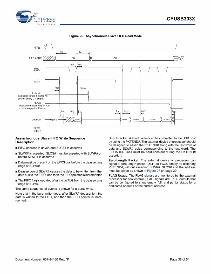
CYUSB303X
Document Number: 001-84160 Rev. *F Page 38 of 54
Figure 26. Asynchronous Slave FIFO Read Mode
Asynchronous Slave FIFO Write Sequence Description
FIFO address is driven and SLCS# is asserted
SLWR# is asserted. SLCS# must be asserted with SLWR# or before SLWR# is asserted
Data must be present on the tWRS bus before the deasserting edge of SLWR#
Deassertion of SLWR# causes the data to be written from the data bus to the FIFO, and then the FIFO pointer is incremented
The FIFO flag is updated after the tWFLG from the deasserting edge of SLWR.
The same sequence of events is shown for a burst write.
Note that in the burst write mode, after SLWR# deassertion, thedata is written to the FIFO, and then the FIFO pointer is incre-mented.
Short Packet: A short packet can be committed to the USB hostby using the PKTEND#. The external device or processor shouldbe designed to assert the PKTEND# along with the last word ofdata and SLWR# pulse corresponding to the last word. TheFIFOADDR lines must be held constant during the PKTEND#assertion.
Zero-Length Packet: The external device or processor cansignal a zero-length packet (ZLP) to FX3S simply by assertingPKTEND#, without asserting SLWR#. SLCS# and the addressmust be driven as shown in Figure 27 on page 39.
FLAG Usage: The FLAG signals are monitored by the externalprocessor for flow control. FLAG signals are FX3S outputs thatcan be configured to show empty, full, and partial status for adedicated address or the current address.
FIFO ADDR
tAS
SLCS
SLRD
tRDl
SLOE
FLAGAdedicated thread Flag for An(1=Not empty 0 = Empty)
tOE
Data Out High-Z
tAH
DN(An)
tRDO tOE tRDOtOH tOH
tRDh
tRDO
tLZ
DN(An) DN(Am) DN+1(Am) DN+2(Am)
SLWR (HIGH)
An Am
FLAGBdedicated thread Flag for Am(1=Not empty 0 = Empty)
tRFLGtFLG

CYUSB303X
Document Number: 001-84160 Rev. *F Page 39 of 54
Figure 27. Asynchronous Slave FIFO Write Mode
Asynchronous Write Cycle Timing
FIFO ADDR
tAS
SLCS
SLWR
tWRl
DATA In High-Z
tAH
DN(An)
tWR
S
tWR
StWRH
tWRh
tWRH
PKTEND
DN(Am) DN+1(Am) DN+2(Am)
SLOE (HIGH)
An Am
FLAGAdedicated thread Flag for An(1=Not Full 0 = Full)
tWFLG
tWFLG
FLAGBdedicated thread Flag for Am(1=Not Full 0 = Full)
tFLG
tWRPE
tWRPE: SLWR# de-assert to PKTEND deassert = 2ns min (This means that PKTEND should not be be deasserted before SLWR#)Note: PKTEND must be asserted at the same time as SLWR#.
Asynchronous ZLP Write Cycle Timing
FIFO ADDR
tAS
SLCS
SLWR(HIGH)
DATA In High-Z
tAH
SLOE (HIGH)
An
FLAGAdedicated thread Flag for An(1=Not Full 0 = Full)
FLAGBdedicated thread Flag for Am(1=Not Full 0 = Full)
PKTEND
tPEl tPEh
tWFLG
tPEh

CYUSB303X
Document Number: 001-84160 Rev. *F Page 40 of 54
Table 13. Asynchronous Slave FIFO Parameters[9]
Parameter Description Min Max Units
tRDI SLRD# low 20 – ns
tRDh SLRD# high 10 – ns
tAS Address to SLRD#/SLWR# setup time 7 – ns
tAH SLRD#/SLWR#/PKTEND to address hold time 2 – ns
tRFLG SLRD# to FLAGS output propagation delay – 35 ns
tFLG ADDR to FLAGS output propagation delay – 22.5
tRDO SLRD# to data valid – 25 ns
tOE OE# low to data valid – 25 ns
tLZ OE# low to data low-Z 0 – ns
tOH SLOE# deassert data output hold – 22.5 ns
tWRI SLWR# low 20 – ns
tWRh SLWR# high 10 – ns
tWRS Data to SLWR# setup time 7 – ns
tWRH SLWR# to Data Hold time 2 – ns
tWFLG SLWR#/PKTEND to Flags output propagation delay – 35 ns
tPEI PKTEND low 20 – ns
tPEh PKTEND high 7.5 – ns
tWRPE SLWR# deassert to PKTEND deassert 2 – ns
Note9. All parameters guaranteed by design and validated through characterization.

CYUSB303X
Document Number: 001-84160 Rev. *F Page 41 of 54
Storage Port Timing
The S0-Port and S1-Port support the MMC Specification Version 4.41 and SD Specification Version 3.0. Table 14 lists the timing parameters for S-Port of the FX3S device.
Table 14. S-Port Timing Parameters[10]
Parameter Description Min Max Units
MMC-20
tSDIS CMD Host input setup time for CMD 4.8 – ns
tSDIS DAT Host input setup time for DAT 4.8 – ns
tSDIH CMD Host input hold time for CMD 4.4 – ns
tSDIH DAT Host input hold time for DAT 4.4 – ns
tSDOS CMD Host output setup time for CMD 5 – ns
tSDOS DAT Host output setup time for DAT 5 – ns
tSDOH CMD Host output hold time for CMD 5 – ns
tSDOH DAT Host output hold time for DAT 5 – ns
tSCLKR Clock rise time – 2 ns
tSCLKF Clock fall time – 2 ns
tSDCK Clock cycle time 50 – ns
SDFREQ Clock frequency – 20 MHz
tSDCLKOD Clock duty cycle 40 60 %
MMC-26
tSDIS CMD Host input setup time for CMD 10 – ns
tSDIS DAT Host input setup time for DAT 10 – ns
tSDIH CMD Host input hold time for CMD 9 – ns
tSDIH DAT Host input hold time for DAT 9 – ns
tSDOS CMD Host output setup time for CMD 3 – ns
tSDOS DAT Host output setup time for DAT 3 – ns
tSDOH CMD Host output hold time for CMD 3 – ns
tSDOH DAT Host output hold time for DAT 3 – ns
tSCLKR Clock rise time – 2 ns
tSCLKF Clock fall time – 2 ns
tSDCK Clock cycle time 38.5 – ns
SDFREQ Clock frequency – 26 MHz
tSDCLKOD Clock duty cycle 40 60 %
MC-HS
tSDIS CMD Host input setup time for CMD 4 – ns
tSDIS DAT Host input setup time for DAT 4 – ns
tSDIH CMD Host input hold time for CMD 3 – ns
tSDIH DAT Host input hold time for DAT 3 – ns
tSDOS CMD Host output setup time for CMD 3 – ns
tSDOS DAT Host output setup time for DAT 3 – ns
tSDOH CMD Host output hold time for CMD 3 – ns
tSDOH DAT Host output hold time for DAT 3 – ns
Note10. All parameters guaranteed by design and validated through characterization.

CYUSB303X
Document Number: 001-84160 Rev. *F Page 42 of 54
tSCLKR Clock rise time – 2 ns
tSCLKF Clock fall time – 2 ns
tSDCK Clock cycle time 19.2 – ns
SDFREQ Clock frequency – 52 MHz
tSDCLKOD Clock duty cycle 40 60 %
MMC-DDR52
tSDIS CMD Host input setup time for CMD 4 – ns
tSDIS DAT Host input setup time for DAT 0.56 – ns
tSDIH CMD Host input hold time for CMD 3 – ns
tSDIH DAT Host input hold time for DAT 2.58 – ns
tSDOS CMD Host output setup time for CMD 3 – ns
tSDOS DAT Host output setup time for DAT 2.5 – ns
tSDOH CMD Host output hold time for CMD 3 – ns
tSDOH DAT Host output hold time for DAT 2.5 – ns
tSCLKR Clock rise time – 2 ns
tSCLKF Clock fall time – 2 ns
tSDCK Clock cycle time 19.2 – ns
SDFREQ Clock frequency – 52 MHz
tSDCLKOD Clock duty cycle 45 55 %
SD-Default Speed (SDR12)
tSDIS CMD Host input setup time for CMD 24 – ns
tSDIS DAT Host input setup time for DAT 24 – ns
tSDIH CMD Host input hold time for CMD 2.5 – ns
tSDIH DAT Host input hold time for DAT 2.5 – ns
tSDOS CMD Host output setup time for CMD 5 – ns
tSDOS DAT Host output setup time for DAT 5 – ns
tSDOH CMD Host output hold time for CMD 5 – ns
tSDOH DAT Host output hold time for DAT 5 – ns
tSCLKR Clock rise time – 2 ns
tSCLKF Clock fall time – 2 ns
tSDCK Clock cycle time 40 – ns
SDFREQ Clock frequency – 25 MHz
tSDCLKOD Clock duty cycle 40 60 %
SD-High-Speed (SDR25)
tSDIS CMD Host input setup time for CMD 4 – ns
tSDIS DAT Host input setup time for DAT 4 – ns
tSDIH CMD Host input hold time for CMD 2.5 – ns
tSDIH DAT Host input hold time for DAT 2.5 – ns
tSDOS CMD Host output setup time for CMD 6 – ns
tSDOS DAT Host output setup time for DAT 6 – ns
tSDOH CMD Host output hold time for CMD 2 – ns
tSDOH DAT Host output hold time for DAT 2 – ns
Table 14. S-Port Timing Parameters[10] (continued)
Parameter Description Min Max Units

CYUSB303X
Document Number: 001-84160 Rev. *F Page 43 of 54
tSCLKR Clock rise time – 2 ns
tSCLKF Clock fall time – 2 ns
tSDCK Clock cycle time 20 – ns
SDFREQ Clock frequency – 50 MHz
tSDCLKOD Clock duty cycle 40 60 %
SD-SDR50
tSDIS CMD Host input setup time for CMD 1.5 – ns
tSDIS DAT Host input setup time for DAT 1.5 – ns
tSDIH CMD Host input hold time for CMD 2.5 – ns
tSDIH DAT Host input hold time for DAT 2.5 – ns
tSDOS CMD Host output setup time for CMD 3 – ns
tSDOS DAT Host output setup time for DAT 3 – ns
tSDOH CMD Host output hold time for CMD 0.8 – ns
tSDOH DAT Host output hold time for DAT 0.8 – ns
tSCLKR Clock rise time – 2 ns
tSCLKF Clock fall time – 2 ns
tSDCK Clock cycle time 10 – ns
SDFREQ Clock frequency 100 MHz
tSDCLKOD Clock duty cycle 40 60 %
SD-DDR50
tSDIS CMD Host input setup time for CMD 4 – ns
tSDIS DAT Host input setup time for DAT 0.92 – ns
tSDIH CMD Host input hold time for CMD 2.5 – ns
tSDIH DAT Host input hold time for DAT 2.5 – ns
tSDOS CMD Host output setup time for CMD 6 – ns
tSDOS DAT Host output setup time for DAT 3 – ns
tSDOH CMD Host output hold time for CMD 0.8 – ns
tSDOH DAT Host output hold time for DAT 0.8 – ns
tSCLKR Clock rise time – 2 ns
tSCLKF Clock fall time – 2 ns
tSDCK Clock cycle time 20 – ns
SDFREQ Clock frequency – 50 MHz
tSDCLKOD Clock duty cycle 45 55 %
Table 14. S-Port Timing Parameters[10] (continued)
Parameter Description Min Max Units

CYUSB303X
Document Number: 001-84160 Rev. *F Page 44 of 54
Serial Peripherals Timing
I2C Timing
Figure 28. I2C Timing Definition

CYUSB303X
Document Number: 001-84160 Rev. *F Page 45 of 54
Table 15. I2C Timing Parameters[11]
Parameter Description Min Max Units
I2C Standard Mode Parameters
fSCL SCL clock frequency 0 100 kHz
tHD:STA Hold time START condition 4 – µs
tLOW LOW period of the SCL 4.7 – µs
tHIGH HIGH period of the SCL 4 – µs
tSU:STA Setup time for a repeated START condition 4.7 – µs
tHD:DAT Data hold time 0 – µs
tSU:DAT Data setup time 250 – ns
tr Rise time of both SDA and SCL signals – 1000 ns
tf Fall time of both SDA and SCL signals – 300 ns
tSU:STO Setup time for STOP condition 4 – µs
tBUF Bus free time between a STOP and START condition 4.7 – µs
tVD:DAT Data valid time – 3.45 µs
tVD:ACK Data valid ACK – 3.45 µs
tSP Pulse width of spikes that must be suppressed by input filter n/a n/a
I2C Fast Mode Parameters
fSCL SCL clock frequency 0 400 kHz
tHD:STA Hold time START condition 0.6 – µs
tLOW LOW period of the SCL 1.3 – µs
tHIGH HIGH period of the SCL 0.6 – µs
tSU:STA Setup time for a repeated START condition 0.6 – µs
tHD:DAT Data hold time 0 – µs
tSU:DAT Data setup time 100 – ns
tr Rise time of both SDA and SCL signals – 300 ns
tf Fall time of both SDA and SCL signals – 300 ns
tSU:STO Setup time for STOP condition 0.6 – µs
tBUF Bus free time between a STOP and START condition 1.3 – µs
tVD:DAT Data valid time – 0.9 µs
tVD:ACK Data valid ACK – 0.9 µs
tSP Pulse width of spikes that must be suppressed by input filter 0 50 ns
I2C Fast Mode Plus Parameters (Not supported at I2C_VDDQ=1.2 V)
fSCL SCL clock frequency 0 1000 kHz
tHD:STA Hold time START condition 0.26 – µs
tLOW LOW period of the SCL 0.5 – µs
tHIGH HIGH period of the SCL 0.26 – µs
tSU:STA Setup time for a repeated START condition 0.26 – µs
Note11. All parameters guaranteed by design and validated through characterization.

CYUSB303X
Document Number: 001-84160 Rev. *F Page 46 of 54
I2S Timing Diagram
Figure 29. I2S Transmit Cycle
tHD:DAT Data hold time 0 – µs
tSU:DAT Data setup time 50 – ns
tr Rise time of both SDA and SCL signals – 120 ns
tf Fall time of both SDA and SCL signals – 120 ns
tSU:STO Setup time for STOP condition 0.26 – µs
tBUF Bus-free time between a STOP and START condition 0.5 – µs
tVD:DAT Data valid time – 0.45 µs
tVD:ACK Data valid ACK – 0.55 µs
tSP Pulse width of spikes that must be suppressed by input filter 0 50 ns
Table 15. I2C Timing Parameters[11] (continued)
Parameter Description Min Max Units
tT
tTR tTFtTL
tThd
tTd
tTH
SCK
SA,WS (output)
Table 16. I2S Timing Parameters[12]
Parameter Description Min Max Units
tT I2S transmitter clock cycle Ttr – ns
tTL I2S transmitter cycle LOW period 0.35 Ttr – ns
tTH I2S transmitter cycle HIGH period 0.35 Ttr – ns
tTR I2S transmitter rise time – 0.15 Ttr ns
tTF I2S transmitter fall time – 0.15 Ttr ns
tThd I2S transmitter data hold time 0 – ns
tTd I2S transmitter delay time – 0.8tT ns
Note tT is selectable through clock gears. Max Ttr is designed for 96-kHz codec at 32 bits to be 326 ns (3.072 MHz).
Note12. All parameters guaranteed by design and validated through characterization.

CYUSB303X
Document Number: 001-84160 Rev. *F Page 47 of 54
SPI Timing Specification
Figure 30. SPI Timing
LSB
LSB
MSB
MSB
LSB
LSB
MSB
MSB
tlead
tsck
tsdd
thoi
twsck twsck
tlag
tdv
trf
tssnh
tdis
tsdi
tlead
tsck
twsck twsck
tlagtrf
tssnh
tsdi
tdis
tdv
thoi
SSN (output)
SCK(CPOL=0, Output)
SCK(CPOL=1, Output)
MISO(input)
MOSI(output)
SSN (output)
SCK(CPOL=0, Output)
SCK(CPOL=1, Output)
MISO(input)
MOSI(output)
SPI Master Timing for CPHA = 0
SPI Master Timing for CPHA = 1
tdi
tdi

CYUSB303X
Document Number: 001-84160 Rev. *F Page 48 of 54
Table 17. SPI Timing Parameters[13]
Parameter Description Min Max Units
fop Operating frequency 0 33 MHz
tsck Cycle time 30 – ns
twsck Clock high/low time 13.5 – ns
tlead SSN-SCK lead time 1/2 tsck[14 ]-5 1.5 tsck[14]+ 5 ns
tlag Enable lag time 0.5 1.5 tsck[14]+5 ns
trf Rise/fall time – 8 ns
tsdd Output SSN to valid data delay time – 5 ns
tdv Output data valid time – 5 ns
tdi Output data invalid 0 – ns
tssnh Minimum SSN high time 10 – ns
tsdi Data setup time input 8 – ns
thoi Data hold time input 0 – ns
tdis Disable data output on SSN high 0 – ns
Notes13. All parameters guaranteed by design and validated through characterization.14. Depends on LAG and LEAD setting in the SPI_CONFIG register.

CYUSB303X
Document Number: 001-84160 Rev. *F Page 49 of 54
Reset Sequence
FX3S’s hard reset sequence requirements are specified in this section.
Figure 31. Reset Sequence
Table 18. Reset and Standby Timing Parameters
Parameter Definition Conditions Min (ms) Max (ms)
tRPW Minimum RESET# pulse widthClock Input 1 –
Crystal Input 1 –
tRH Minimum high on RESET# – 5 –
tRR Reset recovery time (after which Boot loader begins firmware download)
Clock Input 1 –
Crystal Input 5
tSBYTime to enter standby/suspend (from the time MAIN_CLOCK_EN/ MAIN_POWER_EN bit is set) – – 1
tWU Time to wakeup from standbyClock Input 1 –
Crystal Input 5 –
tWH Minimum time before Standby/Suspend source may be reasserted
– 5 –
VDD
( core )
xVDDQ
XTALIN/ CLKIN
RESET #
Mandatory Reset Pulse Hard Reset
tRPW
tRh
Standby/Suspend Source
Standby/Suspend source Is asserted (MAIN_POWER_EN/ MAIN_CLK_EN bit is set)
Standby/Suspend source Is deasserted
tSBY tWU
XTALIN/ CLKIN must be stable before exiting Standby/Suspend
tRR
tWH

CYUSB303X
Document Number: 001-84160 Rev. *F Page 50 of 54
Package Diagram
Figure 32. 121-ball FBGA (10 × 10 × 1.2 mm (0.30 mm Ball Diameter)) Package Outline, 001-54471
001-54471 *D

CYUSB303X
Document Number: 001-84160 Rev. *F Page 51 of 54
Ordering Information
Ordering Code Definitions
Table 19. Device Ordering Information
Ordering Code SRAM (KB) Storage Ports HS-USB OTG GPIF II Data Bus Width Package Type
CYUSB3035-BZXI 512 2 Yes 16-bit 121-ball BGA
CYUSB3035-BZXC 512 2 Yes 16-bit 121-ball BGA
CYUSB3033-BZXC 512 1 Yes 16-bit 121-ball BGA
CYUSB3031-BZXC 256 1 No 16-bit 121-ball BGA
CY
Marketing Code: USB = USB Controller
USB
Company ID: CY = Cypress
Package type: BGA
3 I/C
Temperature range : Industrial/Commercial
Base part number for USB 3.0
XXX BZX
Marketing Part Number

CYUSB303X
Document Number: 001-84160 Rev. *F Page 52 of 54
Acronyms Document Conventions
Units of MeasureAcronym Description
DMA Direct Memory Access
HNP Host Negotiation Protocol
MMC Multimedia Card
MTP Media Transfer Protocol
PLL Phase Locked Loop
PMIC Power Management IC
SD Secure Digital
SDIO Secure Digital Input/Output
SLC Single-Level Cell
SLCS Slave Chip Select
SLOE Slave Output Enable
SLRD Slave Read
SLWR Slave Write
SPI Serial Peripheral Interface
SRP Session Request Protocol
USB Universal Serial Bus
WLCSP Wafer Level Chip Scale Package
Symbol Unit of Measure
°C degree Celsius
Mbps megabits per second
MBps megabytes per second
MHz megahertz
µA microampere
µs microsecond
mA milliampere
ms millisecond
ns nanosecond
ohm
pF picofarad
V volt

CYUSB303X
Document Number: 001-84160 Rev. *F Page 53 of 54
Document History Page
Document Title: CYUSB303X, EZ-USB® FX3S SuperSpeed USB ControllerDocument Number: 001-84160
Revision ECN Orig. of Change
Submission Date Description of Change
** 3786345 SAMT 12/06/2012 New data sheet.
*A 3900859 SAMT 02/11/2013 Updated Ordering Information (Updated part numbers).
*B 4027072 SAMT 06/20/2013 Updated Ordering Information (Updated part numbers).Updated in new template.
*C 4132176 GSZ 09/23/2013 Updated Features.Updated Applications.Updated Functional Overview.Updated Storage Port (S-Port).Replaced CYUSB3035 with CYUSB303X in all instances across the document.
*D 4616283 MDDD 01/07/2015 Added link to related resources on page 1.Added More Information section.
*E 4646195 RAJV 09/18/2015 Updated Slave FIFO Interface and Synchronous Slave FIFO Write Sequence Description.Updated Figure 24 and Figure 25.Updated Table 12.
*F 5085988 ANOP 01/14/2016 No technical updates.Completing Sunset Review.
Document Number: 001-84160 Rev. *F Revised January 14, 2016 Page 54 of 54
EZ-USB™ is a trademark and West Bridge® is a registered trademark of Cypress Semiconductor Corp. All products and company names mentioned in this document may be the trademarks of theirrespective holders.
CYUSB303X
© Cypress Semiconductor Corporation, 2012-2016. The information contained herein is subject to change without notice. Cypress Semiconductor Corporation assumes no responsibility for the use ofany circuitry other than circuitry embodied in a Cypress product. Nor does it convey or imply any license under patent or other rights. Cypress products are not warranted nor intended to be used formedical, life support, life saving, critical control or safety applications, unless pursuant to an express written agreement with Cypress. Furthermore, Cypress does not authorize its products for use ascritical components in life-support systems where a malfunction or failure may reasonably be expected to result in significant injury to the user. The inclusion of Cypress products in life-support systemsapplication implies that the manufacturer assumes all risk of such use and in doing so indemnifies Cypress against all charges.
Any Source Code (software and/or firmware) is owned by Cypress Semiconductor Corporation (Cypress) and is protected by and subject to worldwide patent protection (United States and foreign),United States copyright laws and international treaty provisions. Cypress hereby grants to licensee a personal, non-exclusive, non-transferable license to copy, use, modify, create derivative works of,and compile the Cypress Source Code and derivative works for the sole purpose of creating custom software and or firmware in support of licensee product to be used only in conjunction with a Cypressintegrated circuit as specified in the applicable agreement. Any reproduction, modification, translation, compilation, or representation of this Source Code except as specified above is prohibited withoutthe express written permission of Cypress.
Disclaimer: CYPRESS MAKES NO WARRANTY OF ANY KIND, EXPRESS OR IMPLIED, WITH REGARD TO THIS MATERIAL, INCLUDING, BUT NOT LIMITED TO, THE IMPLIED WARRANTIESOF MERCHANTABILITY AND FITNESS FOR A PARTICULAR PURPOSE. Cypress reserves the right to make changes without further notice to the materials described herein. Cypress does notassume any liability arising out of the application or use of any product or circuit described herein. Cypress does not authorize its products for use as critical components in life-support systems wherea malfunction or failure may reasonably be expected to result in significant injury to the user. The inclusion of Cypress’ product in a life-support systems application implies that the manufacturerassumes all risk of such use and in doing so indemnifies Cypress against all charges.
Use may be limited by and subject to the applicable Cypress software license agreement.
Sales, Solutions, and Legal InformationWorldwide Sales and Design Support
Cypress maintains a worldwide network of offices, solution centers, manufacturer’s representatives, and distributors. To find the office closest to you, visit us at Cypress Locations.
Products
Automotive cypress.com/go/automotive
Clocks & Buffers cypress.com/go/clocks
Interface cypress.com/go/interface
Lighting & Power Control cypress.com/go/powerpsoc
Memory cypress.com/go/memory
PSoC cypress.com/go/psoc
Touch Sensing cypress.com/go/touch
USB Controllers cypress.com/go/USB
Wireless/RF cypress.com/go/wireless
PSoC® Solutions
psoc.cypress.com/solutions
PSoC 1 | PSoC 3 | PSoC 4 | PSoC 5LP
Cypress Developer Community
Community | Forums | Blogs | Video | Training
Technical Support
cypress.com/go/support


![Electrical Compliance Test Specification SuperSpeed ... · [4] USB-IF USB 2.0 Electrical Test Specification, Version 1.03, January 2005. 1.2 USB 2.0 Compliance USB 2,0 testing is](https://img.pdfslide.us/doc/110x75/5f0992bb7e708231d42779b5/electrical-compliance-test-specification-superspeed-4-usb-if-usb-20-electrical.jpg)