Embed Size (px)
Citation preview

Experts in Analog, RF and Mixed-Signal IC Design About AnSem, a Cyient Company
Acquired by Cyient Ltd. in April 2018, AnSem, a Cyient company, is Europe’s leading fabless analog ASIC design service company, designing and delivering state-of-the-art analog, RF, and mixed-signal integrated circuits to customers worldwide. Founded in 1998 and based in Leuven, Belgium, AnSem is an ARM- and TSMC-approved design partner that specializes in the development of advanced integrated circuits for wired and wireless data transmission, sensor data acquisition, ultra-low power, and high-voltage applications. AnSem is ISO 9001 and ISO-13485-2016 certified and is a proven and trustworthy development partner for ambitious and visionary customers reaching for leadership in global markets.
To find out more, please visit the AnSem website at www.ansem.com
AnSem NVEsperantolaan 9 B-3001 Heverlee BelgiumT: +32 16 38 65 00 F: +32 16 38 65 65M: [email protected]
© 2020 Cyient. Cyient believes the information in this publication is accurate as of its publication date; such information is subject to change without notice. Cyient acknowledges the proprietary rights of the trademarks and product names of other companies mentioned in this document.
ANS_BR_TKA_OV_0720
Managing the complete product life cycle, from design requirements to high-volume production
Innovation on chip!
Turnkey analog, RF and mixed-signal ASIC solutions
Wireless data transmission systems have been developed at AnSem since its founding in 1998, making AnSem the leading European independent wireless design center. We cover all aspects of a total solution for wireless systems across a wide frequency range.
Wired data transmission communication systems are developed for high-speed (optical) backend and broadband home networking and industrial busses. AnSem has a large collection of Serdes cores, as well as analog front ends for home access and home networking.
Low-power design in handheld and battery operated systems for consumer applications is well known, but can also be applied in industrial sensors and medical implants. AnSem has been pioneering low-power IC and system design combined with expertise in other domains.
High-voltage circuit designs are useful for low-power applications in medical, industrial and automotive products. AnSem’s deep knowledge of the high-voltage or BCD transistors and processes, combined with special design techniques for low-power consumption, provide optimal solutions.
Data acquisition design solutions are always tailored to the specific requirements of each ASIC. AnSem’s broad library of building blocks is the ideal starting point to bring the highest performance and fastest development time to custom ASIC solutions for sensors and MEMS.
• Full radio concept, architecture and IC circuit design
• DSP-based and hardwired PHY modem implementations
• In-house SW tools for system and IC architecture design
• State-of-the-art validation lab• From 40 KHz for Ultrasonic over all ISM
bands to 6 GHz for professional radio
• SerDes front ends and IOs from 622 Mbps to 10 Gbps
• MIPI PHY interfaces• High-speed home networking:
HomePNA, G.Hn• Solutions for the smart grid:
G3 and Prime • Analog front ends and line drivers for
OFDM communication
• Ultra-low-power wake-up receivers• Remote control for configuration of
medical implants• 200 MHz radio operating from a battery
with as little as 0.9V• Low-power building blocks for the
power management of digital ICs• Ultra-low-power deserialisers (serdes)
up to 6 Gbps
• MI inductive links for short-range energy and data transfer
• Automotive building blocks• MEMS drivers• Bus and cable drivers• Power management building blocks:
DCDC converters, SMPS, Capacitorless LDOs
• Arrays of MEMS switches• Pipeline, SAR, delta-sigma and
cyclic ADC• Current steering DAC• Wheatstone bridge interface for
strain gauge sensor• High-precision (V, T) drivers and signal
conditioning for multiple types of sensors and MEMS
Contact Us
Cyient K.K.Sho-Building 6F, 3-14-5, Nihonbashi,Chuo-Ku, Tokyo, Japan 103-0027T: +81 03 3527 9825 | F: +81 03 3527 9835
North America HeadquartersCyient, Inc.99 East River Drive 5th Floor East Hartford, CT 06108 USAT: +1 860 528 5430 | F: +1 860 528 5873
Europe, Middle East, and Africa Headquarters Cyient Europe Ltd.Apex, Forbury Road,Reading, RG1 1AXUKT: +44 118 3043720
Asia Pacific HeadquartersCyient LimitedLevel 1, 350 Collins StreetMelbourne, Victoria, 3000 AustraliaT: +61 3 8605 4815 | F: +61 3 8601 1180
Global HeadquartersCyient LimitedPlot No. 11 Software Units LayoutInfocity, MadhapurHyderabad - 500081 IndiaT: +91 40 6764 1000 | F: +91 40 2311 0352

Advanced IC Design & Turnkey ASIC Solutions
ASIC Advantages
ASIC Markets
With more than 20 years of hands-on experience, AnSem, a Cyient company, manages the complete product life cycle, from design requirements to high-volume production for clients across the world!
AnSem offers advanced IC design services to (fabless) semiconductor companies and OEMs.
AnSem collaborates with the customers’ IC design groups on IC definition, design, layout and prototype evaluation.
AnSem works closely withcustomers, tailoring the specific ASIC requirements to the detailed system needs.
The chip architecture and circuit topologies are studied and defined, and testability, reliability and qualification requirements are discussed. Then, a final ASIC specification is agreed upon with the customer.
AnSem’s team of expertengineers executes the design, circuit simulations and layout with the latest EDA tools.
Our large analog IP library of proven building block designs, supplemented by the IP libraries of our silicon and IP partners, form the basis for a fast development timeline, meeting customer’s time-to-market requirements.
AnSem takes responsibilityfor manufacturing of the prototypes, coordinating all activities with silicon and packaging suppliers.
The GDS II database is submitted to the foundry. Silicon manufacturing can be done through multi-project wafers or with a multi-layer mask. The prototypes are included in the final production package.
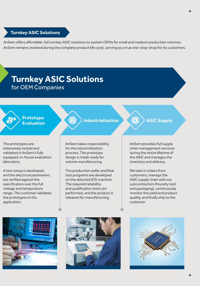
The prototypes areextensively tested and validated in AnSem’s fully equipped, in-house evaluation laboratory.
A test setup is developed, and the electrical parameters are verified against the specification over the full voltage and temperature range. The customer validates the prototypes in the application.
AnSem takes responsibilityfor the industrialization process. The prototype design is made ready for volume manufacturing.
The production wafer and final test programs are developed on the selected ATE machine. The required reliability and qualification tests are performed, and the product is released for manufacturing.
AnSem provides full supplychain management services during the entire lifetime of the ASIC and manages the inventory and delivery.
We take in orders from customers, manage the ASIC supply chain with our subcontractors (foundry test and packaging), continuously monitor the yield and product quality, and finally ship to the customer.
AnSem offers affordable, full turnkey ASIC solutions to system OEMs for small and medium production volumes.
AnSem remains involved during the complete product life cycle, serving as a true one-stop-shop for its customers.
Advanced IC Designfor Semiconductor Companies Turnkey ASIC Solutions
for OEM Companies
• Smaller PCB footprint
• Lower power consumption
• Increased system performance
• Lower system cost
• Higher reliability
• System know-how protection
Definition Phase
Development Phase
Prototype Manufacturing
Prototype Evaluation Industrialization ASIC Supply
Analog, RF and mixed-signal IC design and ASIC supply
Advanced IC Design Turnkey ASIC Solutions
Consumer Communications Automotive
Industrial HealthcareAerospace

Advanced IC Design & Turnkey ASIC Solutions
ASIC Advantages
ASIC Markets
With more than 20 years of hands-on experience, AnSem, a Cyient company, manages the complete product life cycle, from design requirements to high-volume production for clients across the world!
AnSem offers advanced IC design services to (fabless) semiconductor companies and OEMs.
AnSem collaborates with the customers’ IC design groups on IC definition, design, layout and prototype evaluation.
AnSem works closely withcustomers, tailoring the specific ASIC requirements to the detailed system needs.
The chip architecture and circuit topologies are studied and defined, and testability, reliability and qualification requirements are discussed. Then, a final ASIC specification is agreed upon with the customer.
AnSem’s team of expertengineers executes the design, circuit simulations and layout with the latest EDA tools.
Our large analog IP library of proven building block designs, supplemented by the IP libraries of our silicon and IP partners, form the basis for a fast development timeline, meeting customer’s time-to-market requirements.
AnSem takes responsibilityfor manufacturing of the prototypes, coordinating all activities with silicon and packaging suppliers.
The GDS II database is submitted to the foundry. Silicon manufacturing can be done through multi-project wafers or with a multi-layer mask. The prototypes are included in the final production package.
The prototypes areextensively tested and validated in AnSem’s fully equipped, in-house evaluation laboratory.
A test setup is developed, and the electrical parameters are verified against the specification over the full voltage and temperature range. The customer validates the prototypes in the application.
AnSem takes responsibilityfor the industrialization process. The prototype design is made ready for volume manufacturing.
The production wafer and final test programs are developed on the selected ATE machine. The required reliability and qualification tests are performed, and the product is released for manufacturing.
AnSem provides full supplychain management services during the entire lifetime of the ASIC and manages the inventory and delivery.
We take in orders from customers, manage the ASIC supply chain with our subcontractors (foundry test and packaging), continuously monitor the yield and product quality, and finally ship to the customer.
AnSem offers affordable, full turnkey ASIC solutions to system OEMs for small and medium production volumes.
AnSem remains involved during the complete product life cycle, serving as a true one-stop-shop for its customers.
Advanced IC Designfor Semiconductor Companies Turnkey ASIC Solutions
for OEM Companies
• Smaller PCB footprint
• Lower power consumption
• Increased system performance
• Lower system cost
• Higher reliability
• System know-how protection
Definition Phase
Development Phase
Prototype Manufacturing
Prototype Evaluation Industrialization ASIC Supply
Analog, RF and mixed-signal IC design and ASIC supply
Advanced IC Design Turnkey ASIC Solutions
Consumer Communications Automotive
Industrial HealthcareAerospace
Experts in Analog, RF and Mixed-Signal IC Design About AnSem, a Cyient Company
Acquired by Cyient Ltd. in April 2018, AnSem, a Cyient company, is Europe’s leading fabless analog ASIC design service company, designing and delivering state-of-the-art analog, RF, and mixed-signal integrated circuits to customers worldwide. Founded in 1998 and based in Leuven, Belgium, AnSem is an ARM- and TSMC-approved design partner that specializes in the development of advanced integrated circuits for wired and wireless data transmission, sensor data acquisition, ultra-low power, and high-voltage applications. AnSem is ISO 9001 and ISO-13485-2016 certified and is a proven and trustworthy development partner for ambitious and visionary customers reaching for leadership in global markets.
To find out more, please visit the AnSem website at www.ansem.com
AnSem NVEsperantolaan 9 B-3001 Heverlee BelgiumT: +32 16 38 65 00 F: +32 16 38 65 65M: [email protected]
© 2020 Cyient. Cyient believes the information in this publication is accurate as of its publication date; such information is subject to change without notice. Cyient acknowledges the proprietary rights of the trademarks and product names of other companies mentioned in this document.
ANS_BR_TKA_OV_0720
Managing the complete product life cycle, from design requirements to high-volume production
Innovation on chip!
Turnkey analog, RF and mixed-signal ASIC solutions
Wireless data transmission systems have been developed at AnSem since its founding in 1998, making AnSem the leading European independent wireless design center. We cover all aspects of a total solution for wireless systems across a wide frequency range.
Wired data transmission communication systems are developed for high-speed (optical) backend and broadband home networking and industrial busses. AnSem has a large collection of Serdes cores, as well as analog front ends for home access and home networking.
Low-power design in handheld and battery operated systems for consumer applications is well known, but can also be applied in industrial sensors and medical implants. AnSem has been pioneering low-power IC and system design combined with expertise in other domains.
High-voltage circuit designs are useful for low-power applications in medical, industrial and automotive products. AnSem’s deep knowledge of the high-voltage or BCD transistors and processes, combined with special design techniques for low-power consumption, provide optimal solutions.
Data acquisition design solutions are always tailored to the specific requirements of each ASIC. AnSem’s broad library of building blocks is the ideal starting point to bring the highest performance and fastest development time to custom ASIC solutions for sensors and MEMS.
• Full radio concept, architecture and IC circuit design
• DSP-based and hardwired PHY modem implementations
• In-house SW tools for system and IC architecture design
• State-of-the-art validation lab• From 40 KHz for Ultrasonic over all ISM
bands to 6 GHz for professional radio
• SerDes front ends and IOs from 622 Mbps to 10 Gbps
• MIPI PHY interfaces• High-speed home networking:
HomePNA, G.Hn• Solutions for the smart grid:
G3 and Prime • Analog front ends and line drivers for
OFDM communication
• Ultra-low-power wake-up receivers• Remote control for configuration of
medical implants• 200 MHz radio operating from a battery
with as little as 0.9V• Low-power building blocks for the
power management of digital ICs• Ultra-low-power deserialisers (serdes)
up to 6 Gbps
• MI inductive links for short-range energy and data transfer
• Automotive building blocks• MEMS drivers• Bus and cable drivers• Power management building blocks:
DCDC converters, SMPS, Capacitorless LDOs
• Arrays of MEMS switches• Pipeline, SAR, delta-sigma and
cyclic ADC• Current steering DAC• Wheatstone bridge interface for
strain gauge sensor• High-precision (V, T) drivers and signal
conditioning for multiple types of sensors and MEMS
Contact Us
Cyient K.K.Sho-Building 6F, 3-14-5, Nihonbashi,Chuo-Ku, Tokyo, Japan 103-0027T: +81 03 3527 9825 | F: +81 03 3527 9835
North America HeadquartersCyient, Inc.99 East River Drive 5th Floor East Hartford, CT 06108 USAT: +1 860 528 5430 | F: +1 860 528 5873
Europe, Middle East, and Africa Headquarters Cyient Europe Ltd.Apex, Forbury Road,Reading, RG1 1AXUKT: +44 118 3043720
Asia Pacific HeadquartersCyient LimitedLevel 1, 350 Collins StreetMelbourne, Victoria, 3000 AustraliaT: +61 3 8605 4815 | F: +61 3 8601 1180
Global HeadquartersCyient LimitedPlot No. 11 Software Units LayoutInfocity, MadhapurHyderabad - 500081 IndiaT: +91 40 6764 1000 | F: +91 40 2311 0352