Embed Size (px)
Citation preview
CY8CKIT-050 PSoC® 5 DevelopmentKit Guide
Doc. # 001-65816 Rev. *A
Cypress Semiconductor198 Champion Court
San Jose, CA 95134-1709
Phone (USA): 800.858.1810Phone (Intnl): 408.943.2600
http://www.cypress.com
2 CY8CKIT-050 PSoC 5 Development Kit Guide, Doc. # 001-65816 Rev. *A
Copyrights
Copyrights
© Cypress Semiconductor Corporation, 2011. The information contained herein is subject to change without notice. CypressSemiconductor Corporation assumes no responsibility for the use of any circuitry other than circuitry embodied in a Cypressproduct. Nor does it convey or imply any license under patent or other rights. Cypress products are not warranted norintended to be used for medical, life support, life saving, critical control or safety applications, unless pursuant to an expresswritten agreement with Cypress. Furthermore, Cypress does not authorize its products for use as critical components in life-support systems where a malfunction or failure may reasonably be expected to result in significant injury to the user. Theinclusion of Cypress products in life-support systems application implies that the manufacturer assumes all risk of such useand in doing so indemnifies Cypress against all charges.
Any Source Code (software and/or firmware) is owned by Cypress Semiconductor Corporation (Cypress) and is protected byand subject to worldwide patent protection (United States and foreign), United States copyright laws and international treatyprovisions. Cypress hereby grants to licensee a personal, non-exclusive, non-transferable license to copy, use, modify, createderivative works of, and compile the Cypress Source Code and derivative works for the sole purpose of creating custom soft-ware and or firmware in support of licensee product to be used only in conjunction with a Cypress integrated circuit as speci-fied in the applicable agreement. Any reproduction, modification, translation, compilation, or representation of this SourceCode except as specified above is prohibited without the express written permission of Cypress.
Disclaimer: CYPRESS MAKES NO WARRANTY OF ANY KIND, EXPRESS OR IMPLIED, WITH REGARD TO THIS MATE-RIAL, INCLUDING, BUT NOT LIMITED TO, THE IMPLIED WARRANTIES OF MERCHANTABILITY AND FITNESS FOR APARTICULAR PURPOSE. Cypress reserves the right to make changes without further notice to the materials describedherein. Cypress does not assume any liability arising out of the application or use of any product or circuit described herein.Cypress does not authorize its products for use as critical components in life-support systems where a malfunction or failuremay reasonably be expected to result in significant injury to the user. The inclusion of Cypress’ product in a life-support sys-tems application implies that the manufacturer assumes all risk of such use and in doing so indemnifies Cypress against allcharges.
Use may be limited by and subject to the applicable Cypress software license agreement.
PSoC® Creator™ is a trademark and PSoC® is a registered trademark of Cypress Semiconductor Corp. All other trademarksor registered trademarks referenced herein are property of the respective corporations.
Flash Code Protection
Cypress products meet the specifications contained in their particular Cypress PSoC Data Sheets. Cypress believes that itsfamily of PSoC products is one of the most secure families of its kind on the market today, regardless of how they are used.There may be methods, unknown to Cypress, that can breach the code protection features. Any of these methods, to ourknowledge, would be dishonest and possibly illegal. Neither Cypress nor any other semiconductor manufacturer can guaran-tee the security of their code. Code protection does not mean that we are guaranteeing the product as ‘unbreakable’.
Cypress is willing to work with the customer who is concerned about the integrity of their code. Code protection is constantlyevolving. We at Cypress are committed to continuously improving the code protection features of our products.
CY8CKIT-050 PSoC 5 Development Kit Guide, Doc. # 001-65816 Rev. *A 3
Contents
1. Introduction 5
1.1 Kit Contents .................................................................................................................51.2 PSoC Creator ..............................................................................................................51.3 Additional Learning Resources....................................................................................61.4 Document History ........................................................................................................61.5 Documentation Conventions .......................................................................................6
2. Getting Started 72.1 Introduction ..................................................................................................................72.2 CD Installation .............................................................................................................72.3 Install Hardware...........................................................................................................82.4 Install Software ............................................................................................................82.5 Uninstall Software........................................................................................................8
3. Kit Operation 93.1 Introduction ..................................................................................................................93.2 Programming PSoC 5 Device......................................................................................9
4. Hardware 11
4.1 Kit Details...................................................................................................................114.2 Functional Description ...............................................................................................12
4.2.1 Power Supply .................................................................................................124.2.1.1 Power Supply Jumper Settings........................................................134.2.1.2 Grounding Scheme..........................................................................144.2.1.3 Low Power Functionality ..................................................................14
4.2.2 Programming Interface...................................................................................154.2.2.1 On-board Programming Interface ....................................................154.2.2.2 JTAG/SWD Programming................................................................16
4.2.3 USB Communication......................................................................................164.2.4 Boost Convertor .............................................................................................174.2.5 32-kHz and 24-MHz Crystal ...........................................................................184.2.6 PSoC 5 Development Kit Expansion Ports ....................................................18
4.2.6.1 Port D...............................................................................................184.2.6.2 Port E ...............................................................................................20
4.2.7 RS-232 Interface ............................................................................................214.2.8 Prototyping Area ............................................................................................214.2.9 Character LCD ...............................................................................................224.2.10 CapSense Sensors ........................................................................................23
5. Example Projects 25
5.1 Project: VoltageDisplay_SAR_ADC...........................................................................265.1.1 Project Description .........................................................................................26
4 CY8CKIT-050 PSoC 5 Development Kit Guide, Doc. # 001-65816 Rev. *A
Contents
5.1.2 Hardware Connections ..................................................................................265.1.3 SAR ADC Configuration.................................................................................265.1.4 Verify Output ..................................................................................................27
5.2 Project: VoltageDisplay_DelSigADC .........................................................................275.2.1 Project Description.........................................................................................275.2.2 Hardware Connections ..................................................................................275.2.3 Del-Sig ADC Configuration ............................................................................285.2.4 Verify Output ..................................................................................................29
5.3 Project: IntensityLED.................................................................................................295.3.1 Project Description.........................................................................................295.3.2 Hardware Connections ..................................................................................295.3.3 Verify Output ..................................................................................................29
5.4 Project: LowPowerDemo...........................................................................................305.4.1 Project Description.........................................................................................305.4.2 Hardware Connections ..................................................................................305.4.3 Verify Output ..................................................................................................30
5.5 Project: CapSense.....................................................................................................315.5.1 Project Description.........................................................................................315.5.2 Hardware Connections ..................................................................................315.5.3 Verify Output ..................................................................................................32
5.6 Project: ADC_DAC ....................................................................................................335.6.1 Project Description.........................................................................................335.6.2 Hardware Connections ..................................................................................335.6.3 Verify Output ..................................................................................................33
A. Appendix 35
A.1 Schematic..................................................................................................................35A.2 Board Layout .............................................................................................................40
A.2.1 PDC-09356 Top.............................................................................................40A.2.2 PDC-09356 Power .........................................................................................41A.2.3 PDC-09356 Ground .......................................................................................42A.2.4 PDC-09356 Bottom........................................................................................43
A.3 BOM .........................................................................................................................44
CY8CKIT-050 PSoC 5 Development Kit Guide, Doc. # 001-65816 Rev. *A 5
1. Introduction
Thank you for your interest in the CY8CKIT-050 PSoC® 5 Development Kit. This kit allows you todevelop precision analog and low power designs using PSoC 5. You can design your own projectswith PSoC Creator™ or by altering sample projects provided with this kit.
The CY8CKIT-050 PSoC 5 Development Kit is based on the PSoC 5 family of devices. PSoC 5 is aProgrammable System-on-Chip™ platform for 8-bit, 16-bit, and 32-bit applications. It combinesprecision analog and digital logic with a high-performance CPU. With PSoC, you can create theexact combination of peripherals and integrated proprietary IP to meet your applicationrequirements.
1.1 Kit Contents
The PSoC 5 Development Kit contains:
■ Development board
■ Kit CD
■ Quick Start Guide
■ USB A to Mini B cable
■ 3.3 V LCD module
Inspect the contents of the kit; if you find any part missing, contact your nearest Cypress sales officefor help.
1.2 PSoC Creator
Cypress's PSoC Creator software is a state-of-the-art, easy-to-use integrated developmentenvironment (IDE) that introduces a game-changing, hardware and software design environmentbased on classic schematic entry and revolutionary embedded design methodology.
With PSoC Creator, you can:
■ Create and share user-defined, custom peripherals using hierarchical schematic design.
■ Automatically place and route select components and integrate simple glue logic, normally located in discrete muxes.
■ Trade-off hardware and software design considerations allowing you to focus on what matters and getting to market faster.
PSoC Creator also enables you to tap into an entire tools ecosystem with integrated compiler toolchains, RTOS solutions, and production programmers to support both PSoC 3 and PSoC 5.
6 CY8CKIT-050 PSoC 5 Development Kit Guide, Doc. # 001-65816 Rev. *A
Introduction
1.3 Additional Learning Resources
Visit www.cypress.com/go/training for additional learning resources in the form of data sheets,technical reference manual, and application notes.
1.4 Document History
1.5 Documentation Conventions
RevisionPDF Creation
DateOrigin of Change
Description of Change
** 03/01/11 PVKV Initial version of kit guide
*A 04/28/11 RKAD Updated Schematic
Table 1-1. Document Conventions for Guides
Convention Usage
Courier NewDisplays file locations, user entered text, and source code:C:\ ...cd\icc\
ItalicsDisplays file names and reference documentation:Read about the sourcefile.hex file in the PSoC Designer User Guide.
[Bracketed, Bold]Displays keyboard commands in procedures:[Enter] or [Ctrl] [C]
File > OpenRepresents menu paths:File > Open > New Project
BoldDisplays commands, menu paths, and icon names in procedures:Click the File icon and then click Open.
Times New RomanDisplays an equation:2 + 2 = 4
Text in gray boxes Describes cautions or unique functionality of the product.
CY8CKIT-050 PSoC 5 Development Kit Guide, Doc. # 001-65816 Rev. *A 7
2. Getting Started
2.1 Introduction
This chapter describes how to install and configure the PSoC 5 Development Kit. Chapter 3describes the kit operation. It explains how to program a PSoC 5 device with PSoC Programmer anduse the kit with the help of an example project. To reprogram the PSoC device with PSoC Creator,refer to the CD installation instructions for PSoC Creator. Chapter 4 details the hardware operation.Chapter 5 provides instructions to create a simple example project. The Appendix section providesthe schematics and BOM associated with the PSoC 5 Development Kit.
2.2 CD Installation
Follow these steps to install the PSoC 5 Development Kit software:
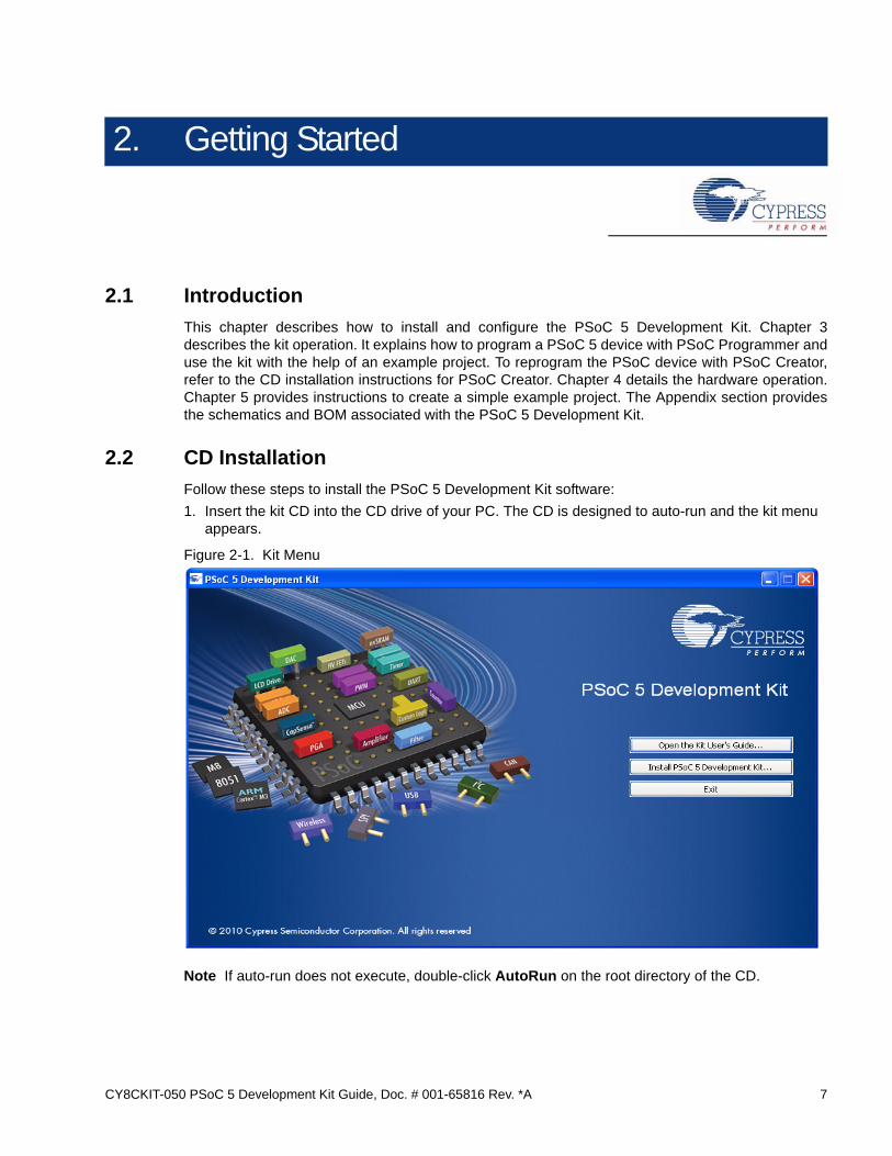
1. Insert the kit CD into the CD drive of your PC. The CD is designed to auto-run and the kit menu appears.
Figure 2-1. Kit Menu
Note If auto-run does not execute, double-click AutoRun on the root directory of the CD.
8 CY8CKIT-050 PSoC 5 Development Kit Guide, Doc. # 001-65816 Rev. *A
Getting Started
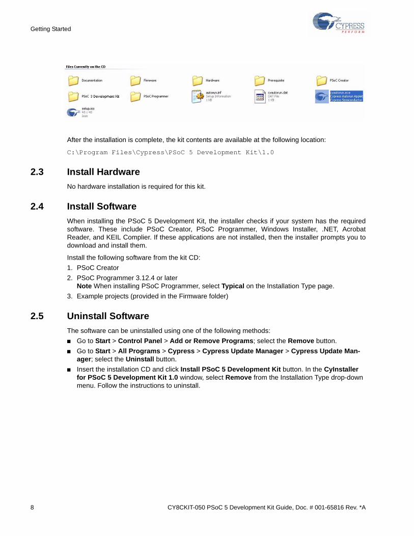
After the installation is complete, the kit contents are available at the following location:
C:\Program Files\Cypress\PSoC 5 Development Kit\1.0
2.3 Install Hardware
No hardware installation is required for this kit.
2.4 Install Software
When installing the PSoC 5 Development Kit, the installer checks if your system has the requiredsoftware. These include PSoC Creator, PSoC Programmer, Windows Installer, .NET, AcrobatReader, and KEIL Complier. If these applications are not installed, then the installer prompts you todownload and install them.
Install the following software from the kit CD:
1. PSoC Creator
2. PSoC Programmer 3.12.4 or laterNote When installing PSoC Programmer, select Typical on the Installation Type page.
3. Example projects (provided in the Firmware folder)
2.5 Uninstall Software
The software can be uninstalled using one of the following methods:
■ Go to Start > Control Panel > Add or Remove Programs; select the Remove button.
■ Go to Start > All Programs > Cypress > Cypress Update Manager > Cypress Update Man-ager; select the Uninstall button.
■ Insert the installation CD and click Install PSoC 5 Development Kit button. In the CyInstaller for PSoC 5 Development Kit 1.0 window, select Remove from the Installation Type drop-down menu. Follow the instructions to uninstall.
CY8CKIT-050 PSoC 5 Development Kit Guide, Doc. # 001-65816 Rev. *A 9
3. Kit Operation
3.1 Introduction
The PSoC 5 Development Kit examples help you develop applications using the PSoC 5 family ofdevices. The kit is designed to develop precision analog applications using PSoC 5. The board alsohas hooks to enable low power measurements for low power application development andevaluation.
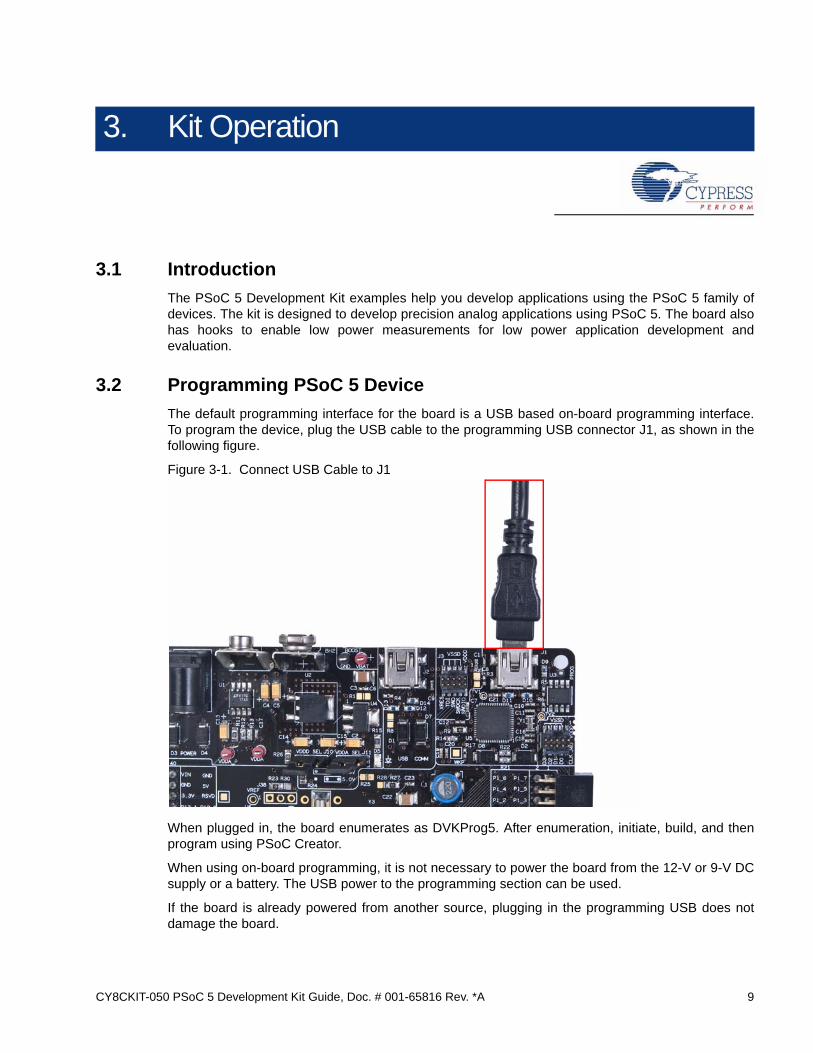
3.2 Programming PSoC 5 Device
The default programming interface for the board is a USB based on-board programming interface.To program the device, plug the USB cable to the programming USB connector J1, as shown in thefollowing figure.
Figure 3-1. Connect USB Cable to J1
When plugged in, the board enumerates as DVKProg5. After enumeration, initiate, build, and thenprogram using PSoC Creator.
When using on-board programming, it is not necessary to power the board from the 12-V or 9-V DCsupply or a battery. The USB power to the programming section can be used.
If the board is already powered from another source, plugging in the programming USB does notdamage the board.
10 CY8CKIT-050 PSoC 5 Development Kit Guide, Doc. # 001-65816 Rev. *A
Kit Operation
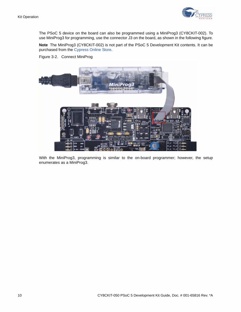
The PSoC 5 device on the board can also be programmed using a MiniProg3 (CY8CKIT-002). Touse MiniProg3 for programming, use the connector J3 on the board, as shown in the following figure.
Note The MiniProg3 (CY8CKIT-002) is not part of the PSoC 5 Development Kit contents. It can bepurchased from the Cypress Online Store.
Figure 3-2. Connect MiniProg
With the MiniProg3, programming is similar to the on-board programmer; however, the setupenumerates as a MiniProg3.
CY8CKIT-050 PSoC 5 Development Kit Guide, Doc. # 001-65816 Rev. *A 11
4. Hardware
4.1 Kit Details
The PSoC 5 Development Kit has the following sections:
■ Power supply system
■ Programming interface
■ USB communications
■ Boost convertor
■ PSoC 5 and related circuitry
■ 32-kHz crystal
■ 24-MHz crystal
■ Port E (analog performance port) and port D (CapSense® or generic port)
■ RS232 communications interface
■ Prototyping area
■ Character LCD interface
■ CapSense buttons and sliders
12 CY8CKIT-050 PSoC 5 Development Kit Guide, Doc. # 001-65816 Rev. *A
Hardware
Figure 4-1. PSoC 5 Development Kit Details
4.2 Functional Description
4.2.1 Power Supply
The power supply system on this board is versatile; input supply can be from the following sources:
■ 9-V or 12-V wall wart supply using connector J4
■ 9-V battery connector using connectors BH1 and BH2
■ USB power from communications section using connector J2
■ USB power from the on-board programming section using connector J1
■ Power from JTAG/SWD programming interface using connector J3
■ Power through boost convertor that uses the input test points VBAT and GND
Power Adapter9V Battery Boost Converter
Input
Communication USB
10-Pin JTAG/SWD/SWODebug and Prog Header
On-BoardProgramming
USB
Port D (CapSense/Miscellaneous
Port)
32 kHz Crystal
Port E(Analog Port)
VariableResistor/
Potentiometer
RS-232Interface
Character LCD Interface Switches/LEDsPrototyping Area
CapSense
RESET Button
10-Pin MiniTraceConnector
CY8CKIT-050 PSoC 5 Development Kit Guide, Doc. # 001-65816 Rev. *A 13
Hardware
The board power domain has five rails:
■ Vin rail: This is where the input of the on-board regulators are connected. This domain is powered through protection diodes.
■ 5-V rail: This is the output of the 5-V regulator U2. The rail is a fixed 5 V output regardless of jumper settings. The voltage in this rail can be less than 5 V only when the board is powered by the USB. This 5-V rail powers the circuits that require fixed 5 V supply.
■ 3.3-V rail: This is the output of the 3.3-V regulator U4. This rail remains 3.3 V regardless of jumper settings or power source changes. It powers the circuits requiring fixed 3.3 V supply such as the on-board programming section.
■ Vddd rail: This rail provides power to the digital supply for the PSoC device. It can be derived from either the 5 V or 3.3 V rail. The selection is made using J10 (3-pin jumper).
■ Vdda rail: This rail provides power to the analog supply of the PSoC device. It is the output of a low noise regulator U1. The regulator is a variable output voltage and can be either 3.3 V or 5 V. This is done by changing the position on J11 (3-pin jumper).
The following block diagram shows the structure of the power system on the board.
Figure 4-2. Power System Structure
4.2.1.1 Power Supply Jumper Settings
Figure 4-3. Jumper Settings
3.3-V Regulator
5-V Regulator
5-V/3.3-V Analog Regulator
USB Communication
Power
9-V Battery
12-V/9-V Wall wart
Vin
Vddd Selection
(J10)
Vdda Selection
(J11)
3.3 V
Vddd
5 V
Vdda
USB Programming 5 V
14 CY8CKIT-050 PSoC 5 Development Kit Guide, Doc. # 001-65816 Rev. *A
Hardware
Two jumpers govern the power rails on the board. J10 is responsible for the selection of Vddd (digitalpower) and J11 selects Vdda (analog power).
The jumper settings for each power scheme are as follows.
Warning:
■ The PSoC device performance is guaranteed when Vdda is greater than or equal to Vddd. Fail-ure to meet this condition can have implications on the silicon performance.
■ When USB power is used, ensure a 3.3 V setting on both analog and digital supplies. This is because, the 5 V rail of the USB power is not accurate and is not recommended.
4.2.1.2 Grounding Scheme
The board is designed considering analog designs as major target applications. Therefore, thegrounding scheme in the board is unique to ensure precision analog performance.
There are three types of ground on this board:
■ GND - This is the universal ground where all the regulators are referred. Both the Vssd and Vssa connect to this ground through a star connection.
■ Vssd - This is the digital ground and covers the digital circuitry present on the board, such as RS232 and LCD.
■ Vssa - This is the analog ground and covers the grounding for analog circuitry present on the board, such as the reference block.
When creating custom circuitry in the prototyping area provided on the board, remember to use theVssa for the sensitive analog circuits and Vssd for the digital ones.
Port E on the board is the designated analog expansion connector. This connector brings outports 0, 3, and 4, which are the best performing analog ports on PSoC 3 and PSoC 5 devices. Theexpansion connector port E has two types of grounds. One is the analog ground (GND_A in silkscreen, Vssa in the schematic), which connects directly to the analog ground on the board. Theother ground known simply as GND, is used for the digital and high current circuitry on theexpansion board. This differentiation on the connector grounds helps the expansion board designerto separate the analog and digital ground on any high precision analog boards being designed forport E.
4.2.1.3 Low Power Functionality
The kit also facilitates application development, which requires low power consumption. Low powerfunctions require a power measurement capability, also available in this kit.
The analog supply is connected to the device through the zero-ohm resistor (R23). By removing thisresistor and connecting an ammeter in series using the test points, Vdda_p and Vdda, you canmeasure the analog power used by the system.
Powering Scheme Jumper Settings
Vdda = 5 V, Vddd = 5 V J10 in 5 V setting and J11 in 5 V setting.
Vdda = 3.3 V, Vddd = 3.3 V J10 in 3.3 V setting and J11 in 3.3 V setting.
Vdda = 5 V, Vddd = 3.3 V J10 in 3.3 V setting and J11 in 5 V setting.
Vdda = 3.3 V, Vddd = 5 VCan be achieved, but is an invalid condition because the PSoC 5 silicon performance cannot be guaranteed.
CY8CKIT-050 PSoC 5 Development Kit Guide, Doc. # 001-65816 Rev. *A 15
Hardware
The digital supply can be monitored by removing connection on the jumper J10 and connecting anammeter in place of the short. This allows to measure the digital power used by the system.
The board provides the ability to measure analog and digital power separately. To measure power ata single point, rather than at analog and digital separately, remove the resistor R23 to disconnect theanalog regulator from powering the Vdda and short Vdda and Vddd through R30. Now, the netpower can be measured at the J10 jumper similar to the digital power measurement. To switchrepeatedly between R23 and R30, moving around the zero-ohm resistors can be discomforting.Hence, a J38 (unpopulated) is provided to populate a male 3-pin header and have a shorting jumperin the place of R23/R30.
While measuring device power, make the following changes in the board to avoid leakage throughother components that are connected to the device power rails.
■ Disconnect the RS232 power by disconnecting R58. An additional jumper capability is available as J37 if you populate it with a 2-pin male header.
■ Disconnect the potentiometer by disconnecting J30.
■ Ground the boost pins if boost operation is not used by populating R1, R28, and R29. Also make sure R25 and R31 are not populated.
4.2.2 Programming Interface
This kit allows programming in two modes:
■ Using the on-board programming interface
■ Using the JTAG/SWD programming interface that uses a MiniProg3
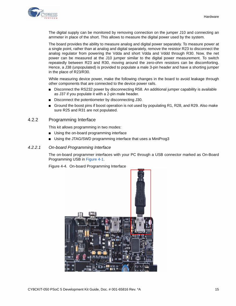
4.2.2.1 On-board Programming Interface
The on-board programmer interfaces with your PC through a USB connector marked as On-BoardProgramming USB in Figure 4-1.
Figure 4-4. On-board Programming Interface
16 CY8CKIT-050 PSoC 5 Development Kit Guide, Doc. # 001-65816 Rev. *A
Hardware
When the USB programming is plugged into the PC, it enumerates as DVKProg5 and you can usethe normal programming interface from PSoC Creator to program this board through the on-boardprogrammer.
A zero-ohm resistor R9 is provided on the board to disconnect power to the on-board programmer.
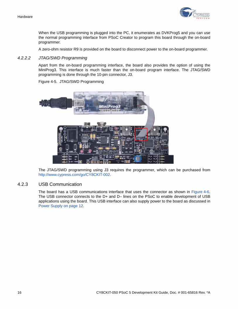
4.2.2.2 JTAG/SWD Programming
Apart from the on-board programming interface, the board also provides the option of using theMiniProg3. This interface is much faster than the on-board program interface. The JTAG/SWDprogramming is done through the 10-pin connector, J3.
Figure 4-5. JTAG/SWD Programming
The JTAG/SWD programming using J3 requires the programmer, which can be purchased fromhttp://www.cypress.com/go/CY8CKIT-002.
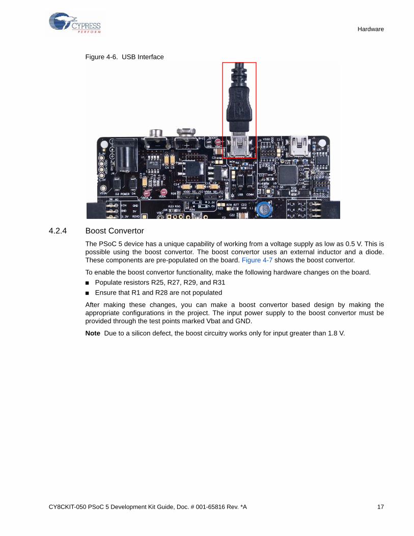
4.2.3 USB Communication
The board has a USB communications interface that uses the connector as shown in Figure 4-6.The USB connector connects to the D+ and D– lines on the PSoC to enable development of USBapplications using the board. This USB interface can also supply power to the board as discussed inPower Supply on page 12.
CY8CKIT-050 PSoC 5 Development Kit Guide, Doc. # 001-65816 Rev. *A 17
Hardware
Figure 4-6. USB Interface
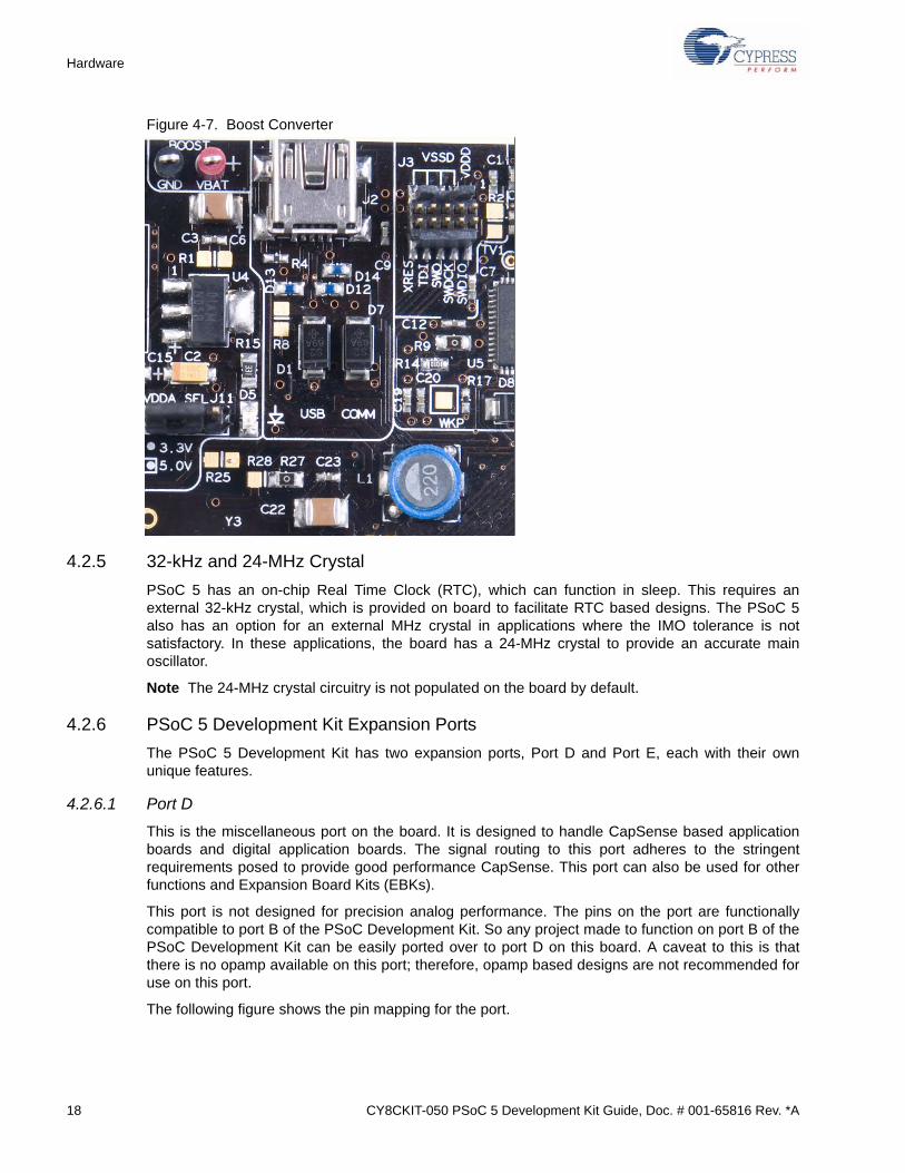
4.2.4 Boost Convertor
The PSoC 5 device has a unique capability of working from a voltage supply as low as 0.5 V. This ispossible using the boost convertor. The boost convertor uses an external inductor and a diode.These components are pre-populated on the board. Figure 4-7 shows the boost convertor.
To enable the boost convertor functionality, make the following hardware changes on the board.
■ Populate resistors R25, R27, R29, and R31
■ Ensure that R1 and R28 are not populated
After making these changes, you can make a boost convertor based design by making theappropriate configurations in the project. The input power supply to the boost convertor must beprovided through the test points marked Vbat and GND.
Note Due to a silicon defect, the boost circuitry works only for input greater than 1.8 V.
18 CY8CKIT-050 PSoC 5 Development Kit Guide, Doc. # 001-65816 Rev. *A
Hardware
Figure 4-7. Boost Converter
4.2.5 32-kHz and 24-MHz Crystal
PSoC 5 has an on-chip Real Time Clock (RTC), which can function in sleep. This requires anexternal 32-kHz crystal, which is provided on board to facilitate RTC based designs. The PSoC 5also has an option for an external MHz crystal in applications where the IMO tolerance is notsatisfactory. In these applications, the board has a 24-MHz crystal to provide an accurate mainoscillator.
Note The 24-MHz crystal circuitry is not populated on the board by default.
4.2.6 PSoC 5 Development Kit Expansion Ports
The PSoC 5 Development Kit has two expansion ports, Port D and Port E, each with their ownunique features.
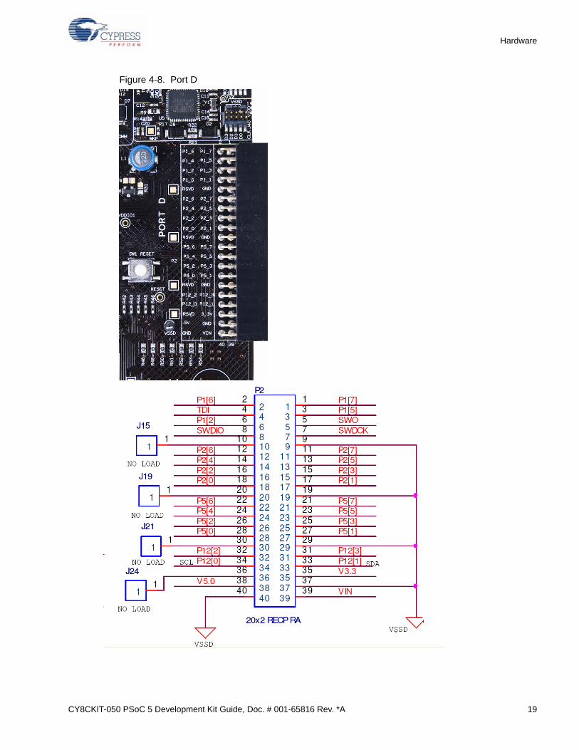
4.2.6.1 Port D
This is the miscellaneous port on the board. It is designed to handle CapSense based applicationboards and digital application boards. The signal routing to this port adheres to the stringentrequirements posed to provide good performance CapSense. This port can also be used for otherfunctions and Expansion Board Kits (EBKs).
This port is not designed for precision analog performance. The pins on the port are functionallycompatible to port B of the PSoC Development Kit. So any project made to function on port B of thePSoC Development Kit can be easily ported over to port D on this board. A caveat to this is thatthere is no opamp available on this port; therefore, opamp based designs are not recommended foruse on this port.
The following figure shows the pin mapping for the port.
CY8CKIT-050 PSoC 5 Development Kit Guide, Doc. # 001-65816 Rev. *A 19
Hardware
Figure 4-8. Port D
20 CY8CKIT-050 PSoC 5 Development Kit Guide, Doc. # 001-65816 Rev. *A
Hardware
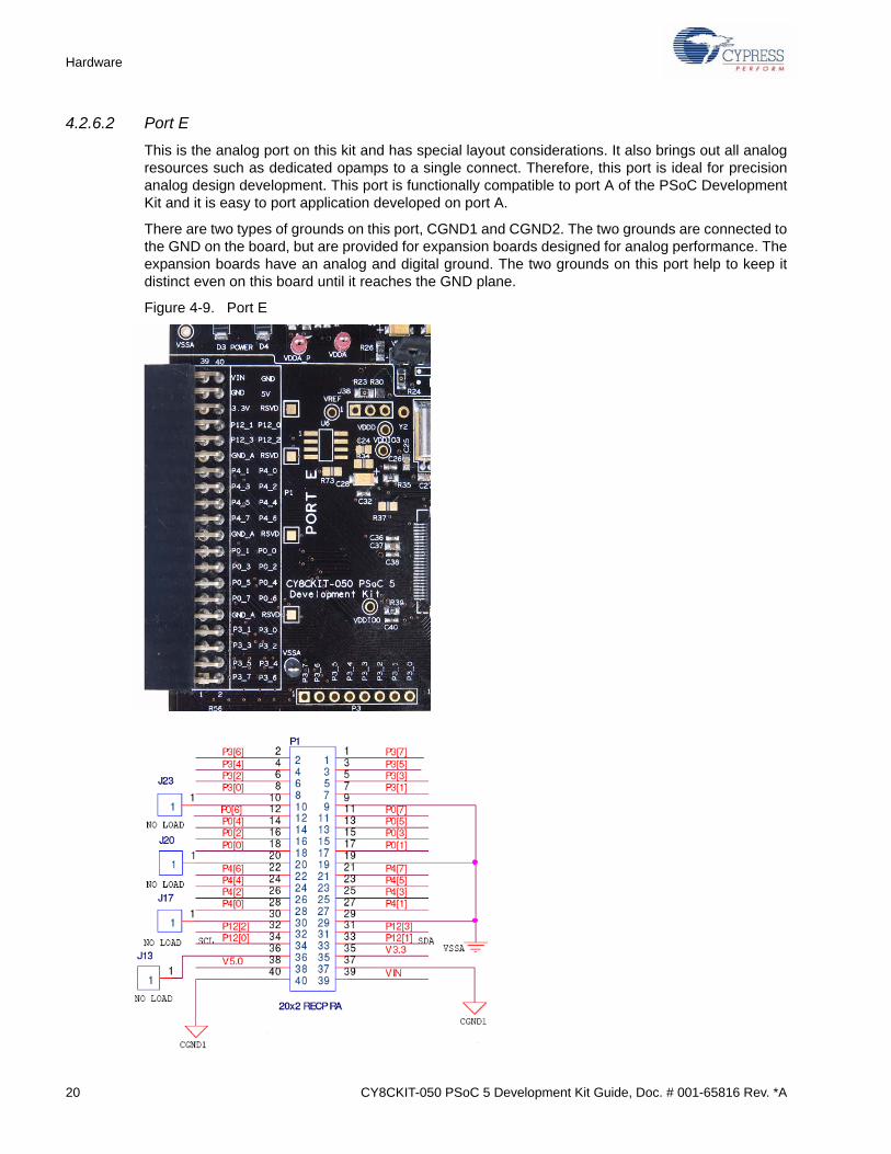
4.2.6.2 Port E
This is the analog port on this kit and has special layout considerations. It also brings out all analogresources such as dedicated opamps to a single connect. Therefore, this port is ideal for precisionanalog design development. This port is functionally compatible to port A of the PSoC DevelopmentKit and it is easy to port application developed on port A.
There are two types of grounds on this port, CGND1 and CGND2. The two grounds are connected tothe GND on the board, but are provided for expansion boards designed for analog performance. Theexpansion boards have an analog and digital ground. The two grounds on this port help to keep itdistinct even on this board until it reaches the GND plane.
Figure 4-9. Port E

CY8CKIT-050 PSoC 5 Development Kit Guide, Doc. # 001-65816 Rev. *A 21
Hardware
4.2.7 RS-232 Interface
The board has an RS-232 transceiver on board for designs using RS-232 (UART). The RS-232section power can be disconnected through a single resistor R58. This is useful for low-powerdesigns.
Figure 4-10. RS-232 Interface
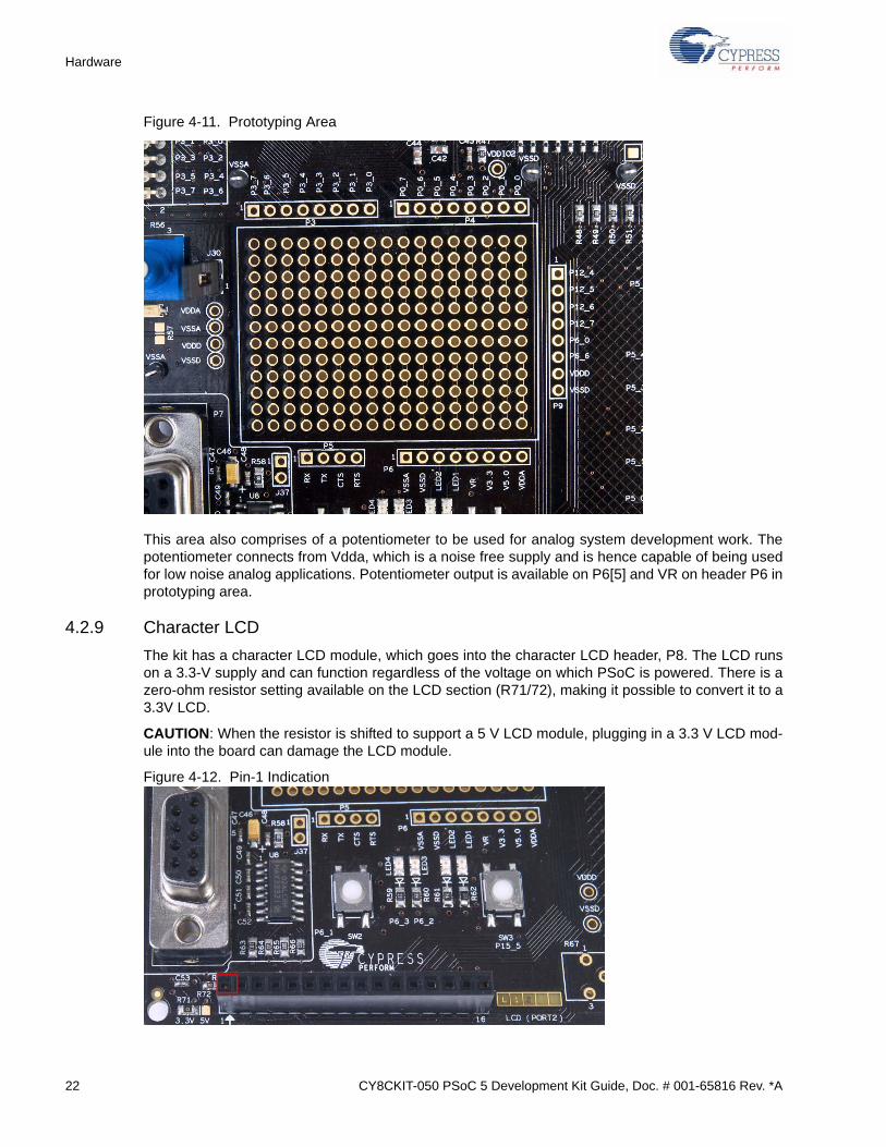
4.2.8 Prototyping Area
The prototyping area on the board has two complete ports of the device for simple custom circuitdevelopment. The ports in the area are port 0 and port 3, which bring out the four dedicated opamppins on the device. Therefore, these ports can be used with the prototyping area to create simple yetelegant analog designs. It also brings SIOs such as port 12[4], port 12[5], port 12[6], and port 12[7]and GPIOs such as port P6[0] and port P6[6]. There is power and ground connections close to theprototyping space for convenience.
The area also has four LEDs and two switches for applications development. The two switches onthe board are hard-wired to port 15[5] and port 6[1]. Two LEDs out of the four are hard-wired to port6[2] and port 6[3] and the other two are brought out on pads closer to the prototyping area.
22 CY8CKIT-050 PSoC 5 Development Kit Guide, Doc. # 001-65816 Rev. *A
Hardware
Figure 4-11. Prototyping Area
This area also comprises of a potentiometer to be used for analog system development work. Thepotentiometer connects from Vdda, which is a noise free supply and is hence capable of being usedfor low noise analog applications. Potentiometer output is available on P6[5] and VR on header P6 inprototyping area.
4.2.9 Character LCD
The kit has a character LCD module, which goes into the character LCD header, P8. The LCD runson a 3.3-V supply and can function regardless of the voltage on which PSoC is powered. There is azero-ohm resistor setting available on the LCD section (R71/72), making it possible to convert it to a3.3V LCD.
CAUTION: When the resistor is shifted to support a 5 V LCD module, plugging in a 3.3 V LCD mod-ule into the board can damage the LCD module.
Figure 4-12. Pin-1 Indication
CY8CKIT-050 PSoC 5 Development Kit Guide, Doc. # 001-65816 Rev. *A 23
Hardware
Figure 4-13. LCD Connected on P8 Connector
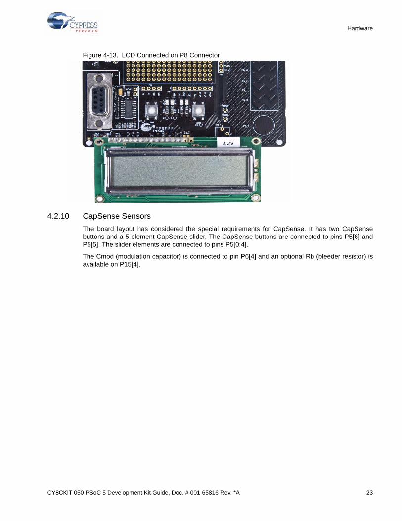
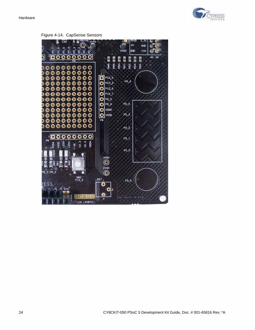
4.2.10 CapSense Sensors
The board layout has considered the special requirements for CapSense. It has two CapSensebuttons and a 5-element CapSense slider. The CapSense buttons are connected to pins P5[6] andP5[5]. The slider elements are connected to pins P5[0:4].
The Cmod (modulation capacitor) is connected to pin P6[4] and an optional Rb (bleeder resistor) isavailable on P15[4].
24 CY8CKIT-050 PSoC 5 Development Kit Guide, Doc. # 001-65816 Rev. *A
Hardware
Figure 4-14. CapSense Sensors
CY8CKIT-050 PSoC 5 Development Kit Guide, Doc. # 001-65816 Rev. *A 25
5. Example Projects
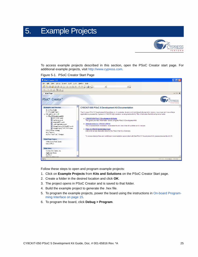
To access example projects described in this section, open the PSoC Creator start page. Foradditional example projects, visit http://www.cypress.com.
Figure 5-1. PSoC Creator Start Page
Follow these steps to open and program example projects:
1. Click on Example Projects from Kits and Solutions on the PSoC Creator Start page.
2. Create a folder in the desired location and click OK.
3. The project opens in PSoC Creator and is saved to that folder.
4. Build the example project to generate the .hex file.
5. To program the example projects, power the board using the instructions in On-board Program-ming Interface on page 15.
6. To program the board, click Debug > Program.
26 CY8CKIT-050 PSoC 5 Development Kit Guide, Doc. # 001-65816 Rev. *A
Example Projects
5.1 Project: VoltageDisplay_SAR_ADC
5.1.1 Project Description
This example code measures an analog voltage controlled by the potentiometer. The code uses theinternal SAR ADC configured for a 12-bit operation; the ADC range is 0 to Vdda. The results are dis-played on the character LCD.
Note The PSoC 5 Development Kit is factory-programmed with this example.
5.1.2 Hardware Connections
The example requires the character LCD on P8. Because it uses the potentiometer, the jumperPOT_PWR should be in place. This connects the potentiometer to the Vdda.
5.1.3 SAR ADC Configuration
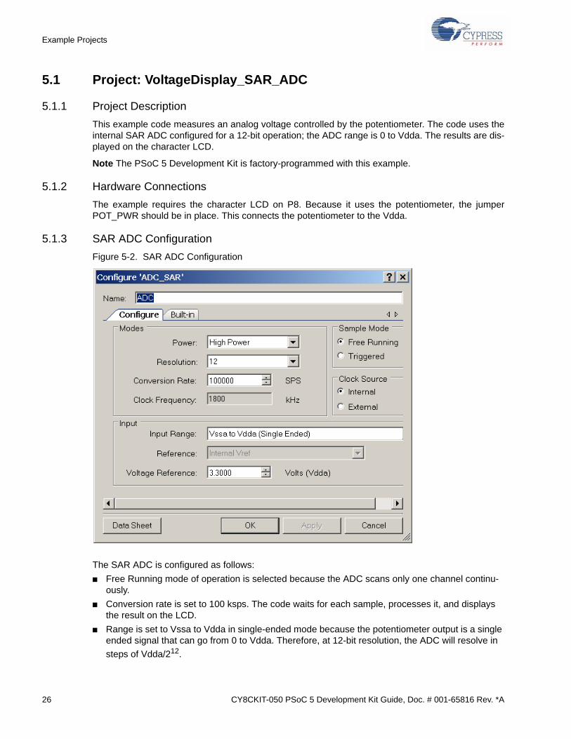
Figure 5-2. SAR ADC Configuration
The SAR ADC is configured as follows:
■ Free Running mode of operation is selected because the ADC scans only one channel continu-ously.
■ Conversion rate is set to 100 ksps. The code waits for each sample, processes it, and displays the result on the LCD.
■ Range is set to Vssa to Vdda in single-ended mode because the potentiometer output is a single ended signal that can go from 0 to Vdda. Therefore, at 12-bit resolution, the ADC will resolve in
steps of Vdda/212.
CY8CKIT-050 PSoC 5 Development Kit Guide, Doc. # 001-65816 Rev. *A 27
Example Projects
■ Voltage Reference should be set to Vdda supply voltage when Input Range is set to ‘Vssa to Vdda’. It is set to 3.3 V here, because by default Vdda jumper setting on the board is set to 3.3 V. If J11 is changed to select 5 V then this parameter should be changed to 5 V accordingly.
5.1.4 Verify Output
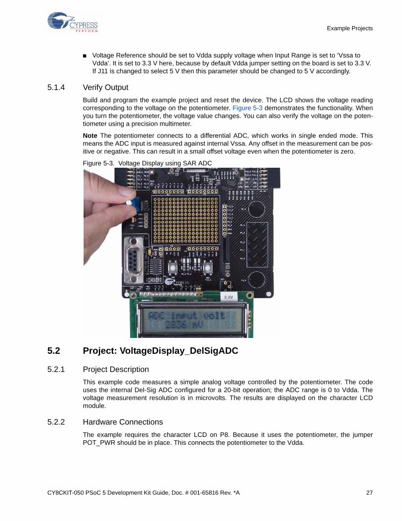
Build and program the example project and reset the device. The LCD shows the voltage readingcorresponding to the voltage on the potentiometer. Figure 5-3 demonstrates the functionality. Whenyou turn the potentiometer, the voltage value changes. You can also verify the voltage on the poten-tiometer using a precision multimeter.
Note The potentiometer connects to a differential ADC, which works in single ended mode. Thismeans the ADC input is measured against internal Vssa. Any offset in the measurement can be pos-itive or negative. This can result in a small offset voltage even when the potentiometer is zero.
Figure 5-3. Voltage Display using SAR ADC
5.2 Project: VoltageDisplay_DelSigADC
5.2.1 Project Description
This example code measures a simple analog voltage controlled by the potentiometer. The codeuses the internal Del-Sig ADC configured for a 20-bit operation; the ADC range is 0 to Vdda. Thevoltage measurement resolution is in microvolts. The results are displayed on the character LCDmodule.
5.2.2 Hardware Connections
The example requires the character LCD on P8. Because it uses the potentiometer, the jumperPOT_PWR should be in place. This connects the potentiometer to the Vdda.
28 CY8CKIT-050 PSoC 5 Development Kit Guide, Doc. # 001-65816 Rev. *A
Example Projects
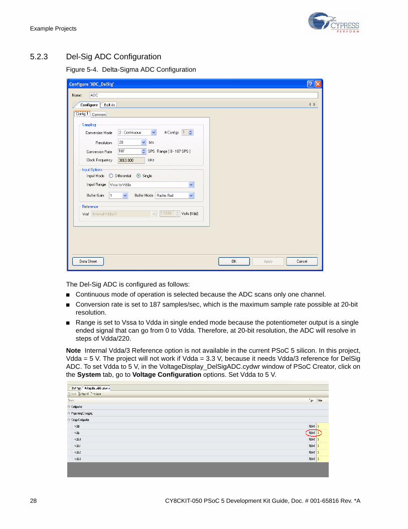
5.2.3 Del-Sig ADC Configuration
Figure 5-4. Delta-Sigma ADC Configuration
The Del-Sig ADC is configured as follows:
■ Continuous mode of operation is selected because the ADC scans only one channel.
■ Conversion rate is set to 187 samples/sec, which is the maximum sample rate possible at 20-bit resolution.
■ Range is set to Vssa to Vdda in single ended mode because the potentiometer output is a single ended signal that can go from 0 to Vdda. Therefore, at 20-bit resolution, the ADC will resolve in steps of Vdda/220.
Note Internal Vdda/3 Reference option is not available in the current PSoC 5 silicon. In this project,Vdda = 5 V. The project will not work if Vdda = 3.3 V, because it needs Vdda/3 reference for DelSigADC. To set Vdda to 5 V, in the VoltageDisplay_DelSigADC.cydwr window of PSoC Creator, click onthe System tab, go to Voltage Configuration options. Set Vdda to 5 V.
CY8CKIT-050 PSoC 5 Development Kit Guide, Doc. # 001-65816 Rev. *A 29
Example Projects
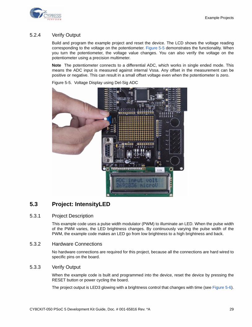
5.2.4 Verify Output
Build and program the example project and reset the device. The LCD shows the voltage readingcorresponding to the voltage on the potentiometer. Figure 5-5 demonstrates the functionality. Whenyou turn the potentiometer, the voltage value changes. You can also verify the voltage on thepotentiometer using a precision multimeter.
Note The potentiometer connects to a differential ADC, which works in single ended mode. Thismeans the ADC input is measured against internal Vssa. Any offset in the measurement can bepositive or negative. This can result in a small offset voltage even when the potentiometer is zero.
Figure 5-5. Voltage Display using Del-Sig ADC
5.3 Project: IntensityLED
5.3.1 Project Description
This example code uses a pulse width modulator (PWM) to illuminate an LED. When the pulse widthof the PWM varies, the LED brightness changes. By continuously varying the pulse width of thePWM, the example code makes an LED go from low brightness to a high brightness and back.
5.3.2 Hardware Connections
No hardware connections are required for this project, because all the connections are hard wired tospecific pins on the board.
5.3.3 Verify Output
When the example code is built and programmed into the device, reset the device by pressing theRESET button or power cycling the board.
The project output is LED3 glowing with a brightness control that changes with time (see Figure 5-6).

30 CY8CKIT-050 PSoC 5 Development Kit Guide, Doc. # 001-65816 Rev. *A
Example Projects
Figure 5-6. Verify Output - Example Project
5.4 Project: LowPowerDemo
5.4.1 Project Description
This example project demonstrates the low power functionality of PSoC 5. The project implementsan RTC based code, which goes to sleep and wakes up on the basis of switch inputs.
The RTC uses an accurate 32-kHz clock generated using the external crystal provided on the board.
When there is a key press, the device is put to sleep while the RTC is kept active.
5.4.2 Hardware Connections
The project requires a 3.3 V LCD to view the time display. No extra connections are required forproject functionality. To make low power measurements using this project, refer and implement thechanges proposed in Low Power Functionality on page 14.
5.4.3 Verify Output
In normal operation, the project displays the time starting from 00:00:00. When you press the SW2button, the device is put to sleep. If an ammeter is connected to measure the system current (referLow Power Functionality on page 14 for details), a system current of less than 2 µA is displayed.
The device wakes up when SW2 is pressed again and displays the time on the LCD. The followingfigures show the output display.
CY8CKIT-050 PSoC 5 Development Kit Guide, Doc. # 001-65816 Rev. *A 31
Example Projects
Figure 5-7. PSoC 5 in Active Mode
Figure 5-8. PSoC 5 in Sleep Mode
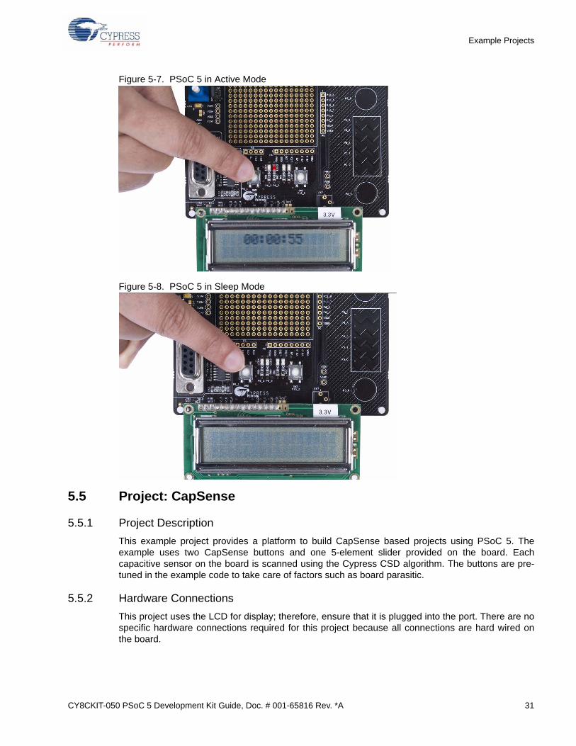
5.5 Project: CapSense
5.5.1 Project Description
This example project provides a platform to build CapSense based projects using PSoC 5. Theexample uses two CapSense buttons and one 5-element slider provided on the board. Eachcapacitive sensor on the board is scanned using the Cypress CSD algorithm. The buttons are pre-tuned in the example code to take care of factors such as board parasitic.
5.5.2 Hardware Connections
This project uses the LCD for display; therefore, ensure that it is plugged into the port. There are nospecific hardware connections required for this project because all connections are hard wired onthe board.
32 CY8CKIT-050 PSoC 5 Development Kit Guide, Doc. # 001-65816 Rev. *A
Example Projects
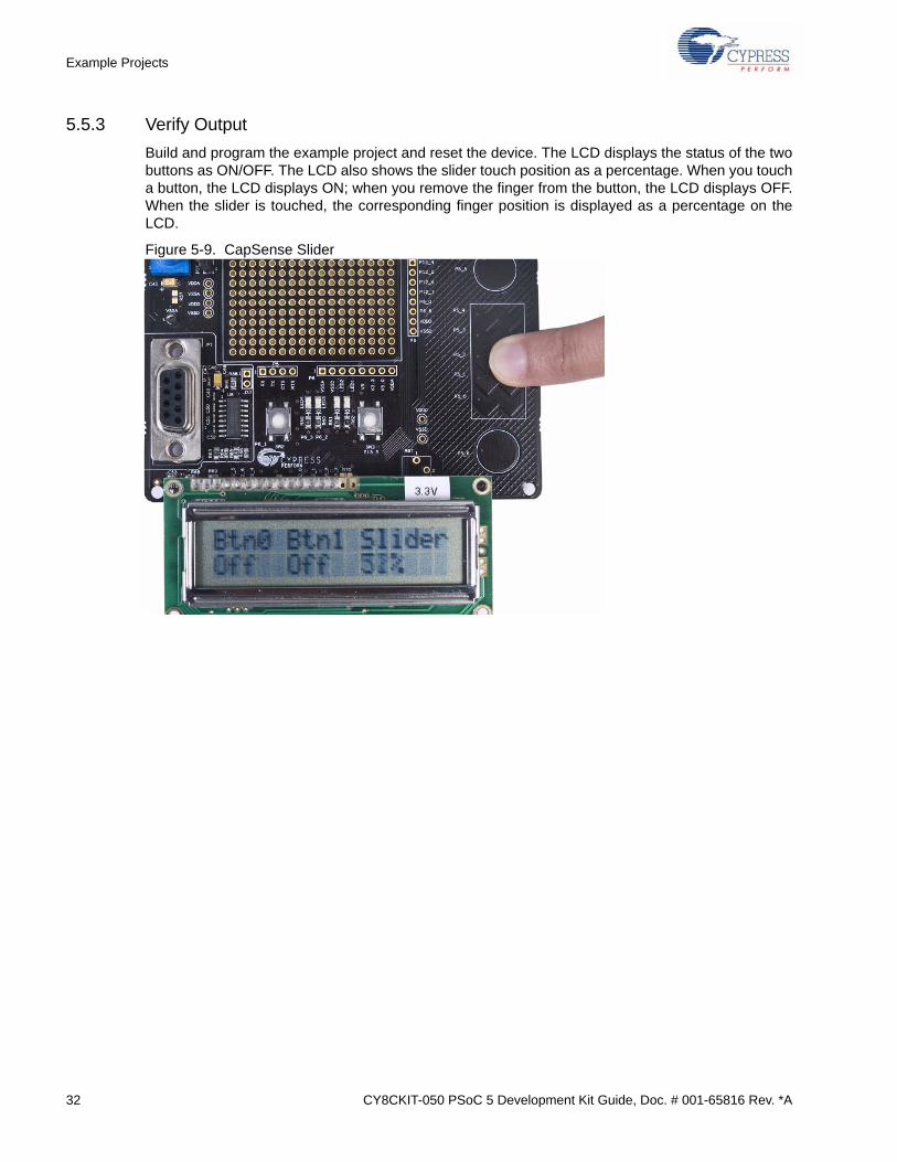
5.5.3 Verify Output
Build and program the example project and reset the device. The LCD displays the status of the twobuttons as ON/OFF. The LCD also shows the slider touch position as a percentage. When you toucha button, the LCD displays ON; when you remove the finger from the button, the LCD displays OFF.When the slider is touched, the corresponding finger position is displayed as a percentage on theLCD.
Figure 5-9. CapSense Slider
CY8CKIT-050 PSoC 5 Development Kit Guide, Doc. # 001-65816 Rev. *A 33
Example Projects
Figure 5-10. CapSense Button
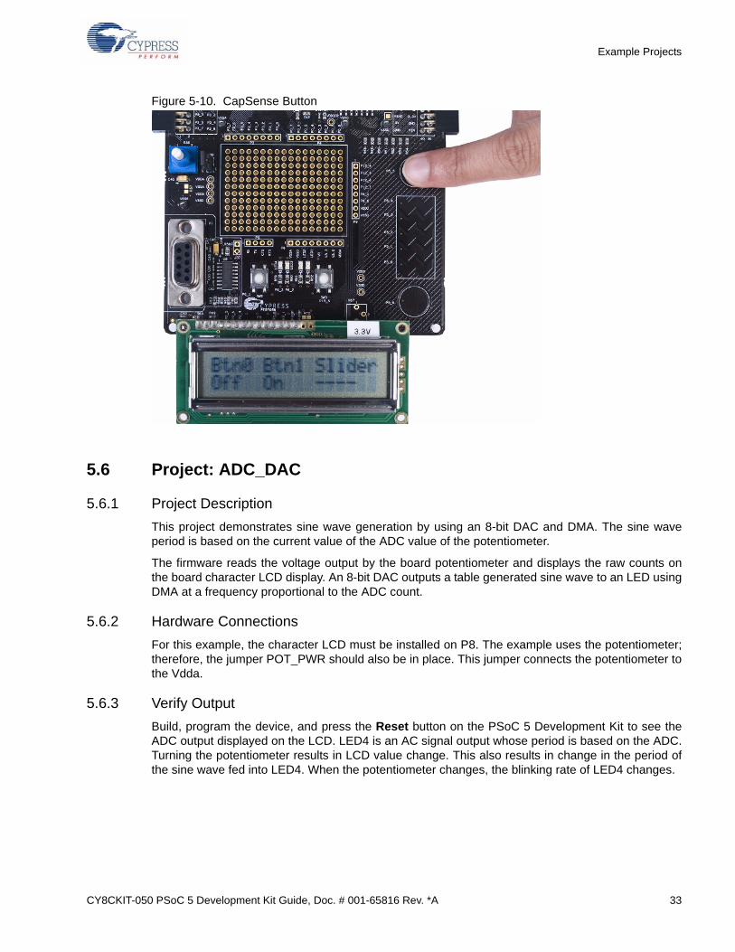
5.6 Project: ADC_DAC
5.6.1 Project Description
This project demonstrates sine wave generation by using an 8-bit DAC and DMA. The sine waveperiod is based on the current value of the ADC value of the potentiometer.
The firmware reads the voltage output by the board potentiometer and displays the raw counts onthe board character LCD display. An 8-bit DAC outputs a table generated sine wave to an LED usingDMA at a frequency proportional to the ADC count.
5.6.2 Hardware Connections
For this example, the character LCD must be installed on P8. The example uses the potentiometer;therefore, the jumper POT_PWR should also be in place. This jumper connects the potentiometer tothe Vdda.
5.6.3 Verify Output
Build, program the device, and press the Reset button on the PSoC 5 Development Kit to see theADC output displayed on the LCD. LED4 is an AC signal output whose period is based on the ADC.Turning the potentiometer results in LCD value change. This also results in change in the period ofthe sine wave fed into LED4. When the potentiometer changes, the blinking rate of LED4 changes.
34 CY8CKIT-050 PSoC 5 Development Kit Guide, Doc. # 001-65816 Rev. *A
Example Projects
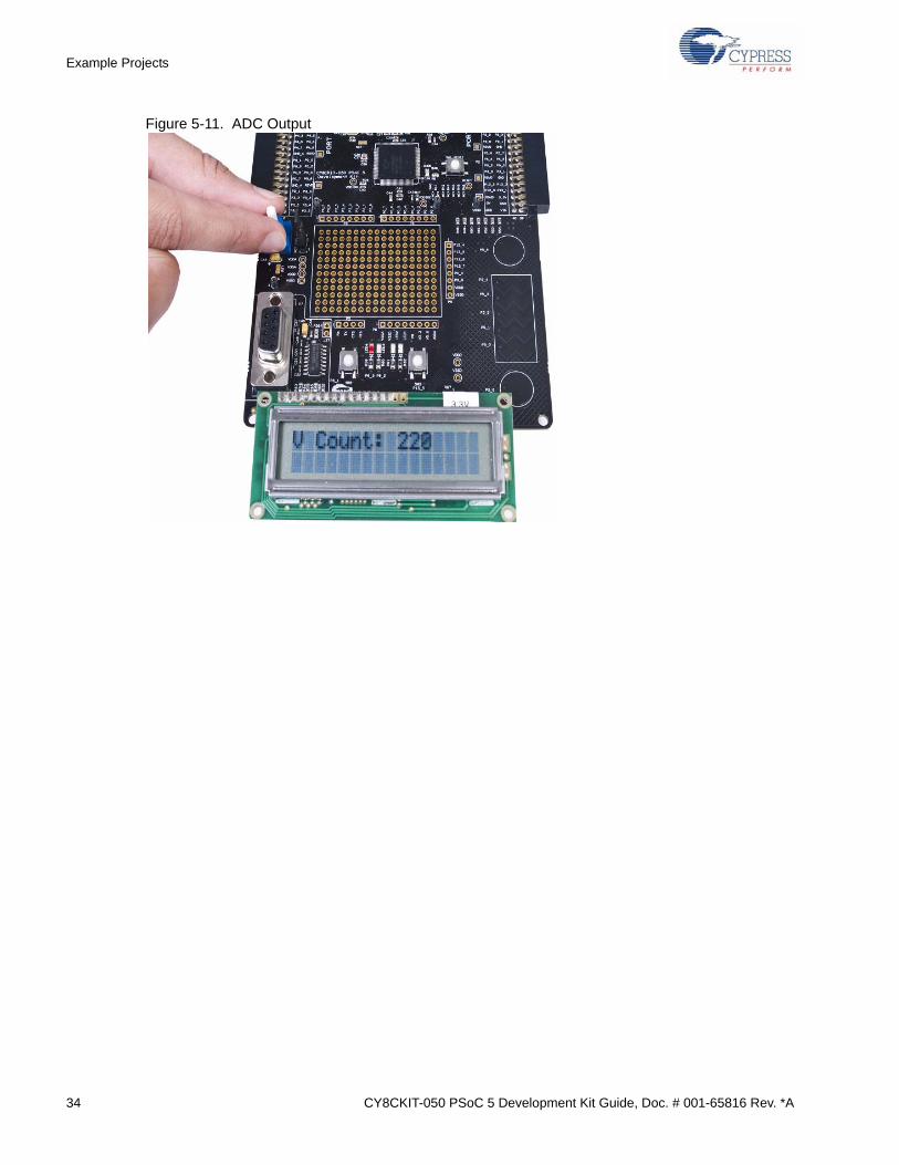
Figure 5-11. ADC Output
CY8CKIT-050 PSoC 5 Development Kit Guide, Doc. # 001-65816 Rev. *A 35
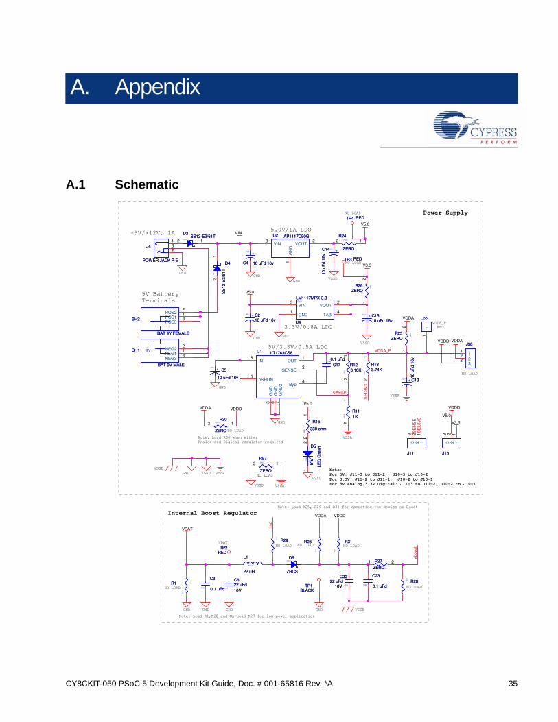
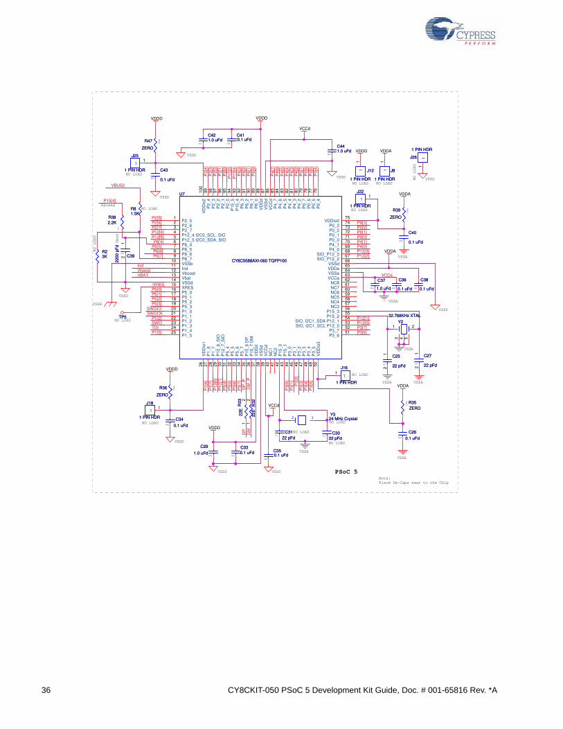
A. Appendix
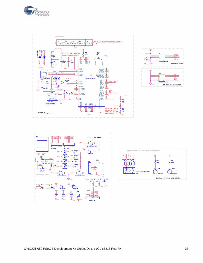
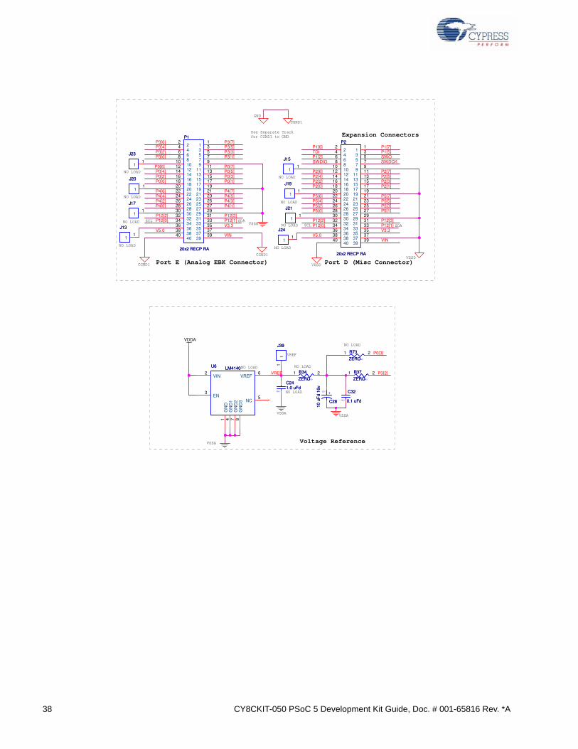
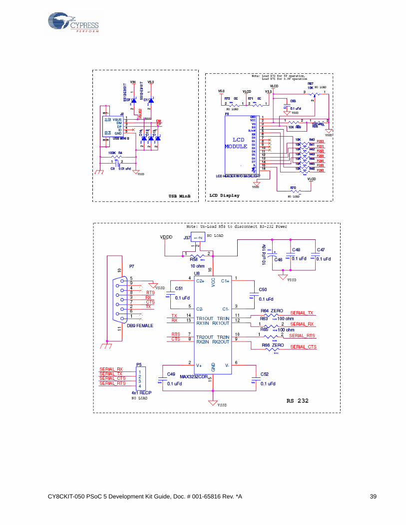
A.1 Schematic
VSSA
VSSD
Note:For 5V: J11-3 to J11-2, J10-3 to J10-2For 3.3V: J11-2 to J11-1, J10-2 to J10-1For 5V Analog,3.3V Digital: J11-3 to J11-2, J10-2 to J10-1
5.0V/1A LDO
3.3V/0.8A LDO
+9V/+12V, 1A
9V BatteryTerminals
VSSB
GND
Power Supply
VSSA
NO LOAD
NO LOAD
VSSD
GND
GNDGND
GND GND
5V/3.3V/0.5A LDO
GND
NO LOAD
GND
Note: Load R30 when either Analog and Digital regulator required
VSSD
NO LOAD
VSSA
VDDA_P RED
VSSD
NO LOAD
VSSAVSSD
NO LOAD
GND GND
NO LOADVBAT
GND
Note: Load R25, R29 and R31 for operating the device on Boost
Note: Load R1,R28 and Un-Load R27 for low power application
NO LOAD
Internal Boost Regulator
NO LOAD
VSSB
NO LOAD
GND
SE
L3V
3
SENSE
SE
NS
ES
EL3
V3
VDDA_P
Ind
Vbo
ost
VDDA
VDDD
V3.3
VDDD
V5.0
V5.0
VDDA
VIN
V3.3
V5.0
VDDD
VDDA
V5.0
VDDA
VBAT
VDDD
+3216 C13
10 u
Fd
16v
+3216 C13
10 u
Fd
16v
TP3 REDTP3 RED
0805
R24
ZERO
0805
R24
ZERO
12
0805R30
ZERO
0805R30
ZERO
12
J38J38
11
22
33
+3216
C4 10 uFd 16v
+3216
C4 10 uFd 16v
0402
C3
0.1 uFd0402
C3
0.1 uFd
0603
R123.16K
0603
R123.16K
12
1210
C622 uFd10V
1210
C622 uFd10V
0805
R23ZERO
0805
R23ZERO
12
TP1BLACK
TP1BLACK
1210
C2222 uFd
10V1210
C2222 uFd
10V
0805
R111K0
805
R111K
12
0805
R57
ZERO
0805
R57
ZERO
12
TP2REDTP2
RED
TP4 REDTP4 RED
TO-252
U2 AP1117D50GTO-252
U2 AP1117D50G
GN
D1
VOUT2
VIN3
J10J101
12
23
3
0805
R27
ZERO 0805
R27
ZERO1 2
0603
R133.74K
0603
R133.74K
12
0402
C170.1 uFd0402
C170.1 uFd
+3216
C5
10 uFd 16v
+3216
C5
10 uFd 16v
U1 LT1763CS8U1 LT1763CS8
IN8
nSHDN5
OUT1
SENSE2
Byp4
GN
D3
GN
D1
6
GN
D2
7
0805
R1
0805
R1
J4
POWER JACK P-5
J4
POWER JACK P-5
1
23
SOT-223
U4
LM1117MPX-3.3SOT-223
U4
LM1117MPX-3.3
GND1
VOUT2
VIN3
TAB4
0805 R29
0805 R29
+3216C14
10 u
Fd
16v
+3216C14
10 u
Fd
16v
+3216 C210 uFd 16v
+3216 C210 uFd 16v
0805
R31
0805
R31
SOT23
D6
ZHCS
SOT23
D6
ZHCS
0805 R28
0805 R28
7032
L1
22 uH
7032
L1
22 uH
0805
R25
0805
R25
0402
C23
0.1 uFd0402
C23
0.1 uFd
BH2
BAT 9V FEMALE
BH2
BAT 9V FEMALE
POS11POS22
POS33
0805
R26ZERO
0805
R26ZERO
12
D-64
D4
SS
12-E
3/61
T
D-64
D4
SS
12-E
3/61
T
21
J11J11
11
22
33
0805
D5
LED
Gre
en
0805
D5
LED
Gre
en
21
+3216 C1510 uFd 16v
+3216 C1510 uFd 16v J33J33
11
D-64
D3SS12-E3/61T
D-64
D3SS12-E3/61T
2 1
9VBH1
BAT 9V MALE
9VBH1
BAT 9V MALE
NEG11NEG22
NEG33
0805
R15
330 ohm
0805
R15
330 ohm
12
36 CY8CKIT-050 PSoC 5 Development Kit Guide, Doc. # 001-65816 Rev. *A
VSSD
NO LOAD
VSSB
NO LOAD
VSSD
VSSA
NO LOAD
VSSD
VSSA
VSSA
NO LOAD
PSoC 5
VSSD
NO LOAD
VSSD
Rbleed
NO LOAD
Cmod
NO LOAD NO LOAD
Note:Place De-Caps near to the Chip
VSSD
VSSD
VSSDNO LOAD
NO LOAD
VSSD
VSSA
NO LOAD
VSSA
VSSA
VSSA
NO LOAD
NO LOAD
P5[
6]P
5[7]
P6[5]P
6[2]
P4[
5]
P5[0]
P12[2]
P1[5]
P0[0]
P4[
6]
P5[1]
P12[3]
/XRES
P5[2]
P4[
7]
P5[3]
SWO
P4[1]
P4[
2]
P6[
3]
P4[
3]P
4[4]
P3[
1]
P0[1]
P6[4]
P15
[5]
P3[
2]
P0[2]
TDI
P2[
0]P
2[1]
P2[
2]
IndVboostVBAT
P2[
3]
SWDCK
P2[
4]
P2[5]
P4[0]
P2[6]
P6[
0]
P2[7]
SWDIOP
0[5]
P0[
4]
P12[0]
P0[
7]
P1[
7]
P3[
3]
P6[
1]
P0[3]
P12[1]
DP
_P
P3[
4]
DM
_P
P3[
0]
P0[
6]
P15
[4]
P3[6]P3[7]
VBUS2
P1[
6]
P12[4]
P6[7]
P15[4]
P12[5]
P12
[6]
P12
[7]
P1[2]
P5[
4]
DM
DP
P3[
5]
P5[
5]
P6[6]
VCCa
VDDA
VDDA
VDDD
VDDD
VCCd
VCCd
VDDD
VDDD
VDDA
VDDD VDDA
J22
1 PIN HDR
J22
1 PIN HDR
11
0603
R382.2K
0603
R382.2K
R23KR23K
0603R36
ZERO
0603R36
ZERO
0402
C26
0.1 uFd0402
C26
0.1 uFd
0402
C40
0.1 uFd0402
C40
0.1 uFd
0402
C350.1 uFd
0402
C350.1 uFd
J12
1 PIN HDR
J12
1 PIN HDR
11
0402
C38
0.1 uFd0402
C38
0.1 uFd
J25
1 PIN HDR
J25
1 PIN HDR
11
0402
C43
0.1 uFd0402
C43
0.1 uFd
U7
CY8C5588AXI-060 TQFP100
U7
CY8C5588AXI-060 TQFP100
P2_51
P2_62
P2_73
P12_4 I2C0_SCL, SIO4
P12_5 I2C0_SDA, SIO5
P6_46
P6_57
P6_68
P6_79
VSSb10
Ind11
Vboost12
Vbat13
VSSd14
XRES15
P5_016
P5_117
P5_218
P5_319
P1_020
P1_121
P1_222
P1_323
P1_424
P1_525
VD
Dio
126
P1_
627
P1_
728
P12
_6_S
IO29
P12
_7_S
IO30
P5_
431
P5_
532
P5_
633
P5_
734
P15
_6 D
P35
P15
_7 D
M36
VD
Dd
37
VS
Sd
38
VC
Cd
39
NC
140
NC
241
P15
_042
P15
_143
P3_
044
P3_
145
P3_
246
P3_
347
P3_
448
P3_
549
VD
Dio
350
VDDio075
P0_374
P0_273
P0_172
P0_071
P4_170
P4_069
SIO_P12_368
SIO_P12_267
VSSd66
VDDa65
VSSa64
VCCa63
NC862
NC761
NC660
NC559
NC458
NC357
P15_356
P15_255
SIO, I2C1_SDA P12_154
SIO, I2C1_SCL P12_053
P3_752
P3_651
P2_
499
P2_
398
P2_
297
P2_
196
P2_
095
P15
_594
P15
_493
P6_
392
P6_
291
P6_
190
P6_
089
VD
Dd
88
VS
Sd
87
VC
Cd
86
P4_
785
P4_
684
P4_
583
P4_
482
P4_
381
P4_
280
P0_
779
P0_
678
P0_
577
P0_
476
VD
Dio
210
0
0402
C3022 pFd
0402
C3022 pFd
0402
C410.1 uFd
0402
C410.1 uFd
R81.5KR81.5K
TP5TP5
0603
C421.0 uFd
0603
C421.0 uFd
J18
1 PIN HDR
J18
1 PIN HDR
11
0603R
3322
E
0603R
3322
E1
2
0402
C330.1 uFd
0402
C330.1 uFd
0603 R
3222
E
0603 R
3222
E1
2
0402
C34
0.1 uFd0402
C34
0.1 uFd
0603R47
ZERO
0603R47
ZERO
0603
C25
22 pFd0603
C25
22 pFd
12
0603
C29
1.0 uFd0603
C29
1.0 uFd
0603R39
ZERO
0603R39
ZERO
0402
C3122 pFd
0402
C3122 pFd
0603
C441.0 uFd
0603
C441.0 uFd
2 1Y3
24 MHz Crystal2 1Y3
24 MHz Crystal
0402
C36
0.1 uFd0402
C36
0.1 uFd
0603 R35
ZERO
0603 R35
ZERO
J16
1 PIN HDR
J16
1 PIN HDR
11
0603
C37
1.0 uFd0603
C37
1.0 uFd
0603
C27
22 pFd0603
C27
22 pFd
12
Y2
32.768KHz XTAL
Y2
32.768KHz XTAL
1 2
3 4 5
0805
C39
2200
pF
d
0805
C39
2200
pF
d1
2
J26
1 PIN HDR
J26
1 PIN HDR
11
J8
1 PIN HDR
J8
1 PIN HDR
11
CY8CKIT-050 PSoC 5 Development Kit Guide, Doc. # 001-65816 Rev. *A 37
GND
PLACE ONE CAP PER EACH VCC ON U5.
PLACE C11 AND C16 CLOSECLOSE TO U5-3 AND U5-7.
TP2
GND
NO LOAD
GND
GND
FX2LP Programmer GND
FIRMWARE UPDATEREQUIRED FOR
GND
GND
GND
USB BACKVOLTAGECOMPLIANCE.
GND
VSSD VSSDSWD/SWV/JTAG
VSSD10-PIN TRACE HEADER
SWDIOSWDCK
3V3_FX12P
SWO
/XRES
D+VBUS1
VBUS1
D-
3V3_FX12P
VB
US
1
3V3_FX12P
VB
US
1
SWO
/XRES
SWDCK
TDI
P2[5]
P2[7]
P2[4]
P2[6]
P2[3]
SWDIO
V3.3
VIN V5.0VDDD
VDDD
0402
C20
0.1 uFd0402
C20
0.1 uFd
TV2TV-20R
TV2TV-20R
1
0402
R62.2K0
402
R62.2K
0402
C1
0.1 uFd0402
C1
0.1 uFd
D-64
D8
SS
12-E
3/61
TD-64
D8
SS
12-E
3/61
T
21
D-64
D9
D-64
D9
21
J9J9
11
D-64
D11
D-64
D11
21
D-64
D10
D-64
D10
21
J1
USB MINI B
J1
USB MINI B
VBUS1
DM2
DP3
GND5ID4
S1
6
S2
7S
38
S4
9
J40
50MIL KEYED SMD
J40
50MIL KEYED SMD
13579
2468
10
0402
C112.2 uFd6.3V
0402
C112.2 uFd6.3V
0402
R3
100K0402
R3
100K
0603
R14100K1%0
603
R14100K1%
12
0603 R21
39K1%
0603 R21
39K1%
12
0402C8
0.01 uFd
0402C8
0.01 uFd
1 2
0402
C21
0.1 uFd0402
C21
0.1 uFd
U5
CY7C68013A-56LTXC
U5
CY7C68013A-56LTXC
RE
SE
RV
ED
14
WAKEUP#44
PA1/nINT134
SCL15
VC
C5
43
SDA16
PA2/SLOE35
VC
C3
17
PA3/WU236
VC
C4
27
PA4/FIFOADR037
PA5/FIFOADR138
AVCC13
PA6/PKTEND39
GN
D3
26
PA7/FLAGD40
GN
D4
28
PB0/FD018
GN
D6
56
AG
ND
16
XT
ALI
N5
XT
ALO
UT
4
PA0/nINT033
PB1/FD119
PB2/FD220
PB3/FD321
PB4/FD422
PB5/FD523
PB6/FD624
PB7/FD725
DPLUS8 DMINUS9
CLKOUT54
RESET#42
VC
C6
55
RDY0/SLRD1
RDY1/SLWR2
CTL0/FLAGA29
CTL1/FLAGB30
CTL2/FLAGC31
IFCLK13
PD0/FD845
PD1/FD946
PD2/FD1047
PD3/FD1148
PD4/FD1249
PD5/FD1350
PD6/FD1451
PD7/FD1552
VC
C1
11
VC
C2
32
GN
D1
12
GN
D2
41
AG
ND
210
AVCC27
GN
D5
53
CP
57
0805
R9ZERO
0805
R9ZERO
12
0402
R17
10K
0402
R17
10K
D-64
D2
SS
12-E
3/61
TD-64
D2
SS
12-E
3/61
T
21
0402
C18
0.1 uFd0402
C18
0.1 uFd
0402
C19
0.1 uFd0402
C19
0.1 uFd
8-SOIC
U3
24LC00/SN 8-SOIC
8-SOIC
U3
24LC00/SN 8-SOIC
SDA5
NC
11
NC
22
NC
33
VCC8 SCL
6
NC
47
GND4
0402
C10
0.1 uFd0402
C10
0.1 uFd0402
C12
0.1 uFd0402
C12
0.1 uFd
J3
50MIL KEYED SMD
J3
50MIL KEYED SMD
13579
2468
10
Y124 MHz
Y124 MHz
13
2
0603 R22
62K1%
0603 R22
62K1%
12
0402
R52.2K0
402
R52.2K
TV1TV11
0402
C7
0.1 uFd0402
C7
0.1 uFd
0402
C16
0.1 uFd0402
C16
0.1 uFd
NO LOAD
NO LOAD
VSSA
NO LOAD
NO LOADVSSA
VSSD
NO LOAD
VSSA
NO LOAD
VSSD
NO LOAD
VSSA
NO LOAD
NO LOAD
VSSD
VSSD
VSSD
Prototype Area
VSSA
NO LOAD
Note: Load R56 for high precision analog
VSSA
VSSD
VSSD
VSSD
VSSD
NO LOAD
NO LOAD
NO LOAD
NO LOAD
CapSense Button and Slider
Note: Un-Load R48 - R54 to disconnect Capacitive Sensors
P0[
2]
P6[5]
P0[
3]
LED1
P0[
4]
LED2
P0[
5]P
0[6]
P0[
7]
P6[5]
P6[1]
P6[2]
P3[
0]P
3[1]
P3[
2]
P15[5]
P3[
3]P
3[4]
P3[
5]P
3[6]
P3[
7]
P6[3]
P12
[7]
LED1
P0[
0]
P12
[4]
P6[
0]
P6[5]
/XRES
P12
[5]
P0[
1]
P6[
6]
P12
[6]
LED2
P5[
0]
P5[
5]
P5[
1]
P5[
2]
P5[
6]
P5[
3]
P5[
4]
VDDD VDDA
VDDD
V3.3V5.0
VDDD
VDDA
VDDA
VDDA
VDDD
J27
1 PIN HDR
J27
1 PIN HDR
11
0603
R49
ZE
RO
0603
R49
ZE
RO
J6
1 PIN HDR
J6
1 PIN HDR
11
0805
R62 330 ohm
0805
R62 330 ohm
1 2
CSB1
CapSense
CSB1
CapSense
1
SW3
SW PUSHBUTTON
SW3
SW PUSHBUTTON
1A1B
2A2B CSS1
CapSense Linear Slider 5 SegCSS1CapSense Linear Slider 5 Seg
1 2 3 4 5
+3216
C45
10 u
Fd
16v
+3216
C45
10 u
Fd
16v 0805
R60 330 ohm
0805
R60 330 ohm
1 2
P4RECP 8X1P4RECP 8X1
11
22
33
44
55
66
77
88
J34J34
11
0805
LED4
LED Red
0805
LED4
LED Red
2 1
J30J30
11
22
0603
R52
ZE
RO
0603
R52
ZE
RO 0603
R54
ZERO0603
R54
ZEROR56POT 10K R56POT 10K
13
2
0805
LED1
LED Red
0805
LED1
LED Red
2 1
0805
R59 330 ohm
0805
R59 330 ohm
1 2
SW1
SW PUSHBUTTON
SW1
SW PUSHBUTTON
1A1B
2A2B
0603
R53
ZE
RO
0603
R53
ZE
RO
0805
LED3
LED Red
0805
LED3
LED Red
2 1
R55 10KR55 10K
1 3
2
P6P6
1122334455667788
SW2
SW PUSHBUTTON
SW2
SW PUSHBUTTON
1A1B
2A2B
J7
1 PIN HDR
J7
1 PIN HDR
11
J31J31
11
J32J32
11
J5
1 PIN HDR
J5
1 PIN HDR
11
0603
R50
ZE
RO
0603
R50
ZE
RO
J35
1 PIN HDR
J35
1 PIN HDR
11
P3RECP 8X1P3RECP 8X1
11
22
33
44
55
66
77
88
0805
LED2
LED Red
0805
LED2
LED Red
2 1
P9 RECP 8X1P9 RECP 8X1
11
22
33
44
55
66
77
88
J14
1 PIN HDR
J14
1 PIN HDR
11
J28
1 PIN HDR
J28
1 PIN HDR
11
0805
R61 330 ohm
0805
R61 330 ohm
1 2
0603
R51
ZE
RO
0603
R51
ZE
RO
J36
1 PIN HDR
J36
1 PIN HDR
11
J29J29
11
J50
Breadboard
J50
Breadboard
0603
R48
ZERO0603
R48
ZERO
CSB2
CapSense
CSB2
CapSense
1
38 CY8CKIT-050 PSoC 5 Development Kit Guide, Doc. # 001-65816 Rev. *A
VSSDCGND1
VSSDCGND1
SDASCL
CGND1
GND
NO LOAD
SDASCL
Port E (Analog EBK Connector) Port D (Misc Connector)
NO LOAD
NO LOAD
NO LOAD
NO LOAD
NO LOAD
Expansion Connectors
VSSA NO LOAD
NO LOAD
Use Separate Trackfor CGND1 to GND
NO LOAD
Voltage ReferenceVSSA
VSSA
NO LOAD
NO LOAD
VSSA
NO LOAD
VREF
P2[4]P2[2]P2[0]
P2[6]
P5[6]
P5[0]P5[2]P5[4]
P1[2]
P1[6]TDI
SWDIOSWOSWDCK
P12[1]P12[3]
P1[7]P1[5]
P12[0]P12[2]
VIN
V3.3V5.0
P3[2]
P3[6]P3[4]
P3[0]P3[3]P3[1]
P12[1]
P0[7]P0[5]
P4[3]P4[1]
P12[3]
P3[7]P3[5]
P0[6]
P0[3]P0[1]
P4[7]P4[5]P4[4]
P4[2]P4[0]
P12[0]P12[2]
P0[4]P0[2]P0[0]
P4[6]
VIN
V3.3V5.0
P2[3]P2[1]
P2[7]P2[5]
P5[7]P5[5]P5[3]P5[1]
P3[2]
P0[3]
VREF
VDDA
0603
C241.0 uFd
0603
C241.0 uFd
+3216
C28
10 u
Fd
16v
+3216
C28
10 u
Fd
16v
J21J21
11
P2
20x2 RECP RA
P2
20x2 RECP RA
11
22
33
44
55
66
77
88
99
1010
1111
1212
1313
1414
1515
1616
1717
1818
1919
2020
2121
2323
2525
2727
2929
3131
3333
3535
3737
3939
2222
2424
2626
2828
3030
3232
3434
3636
3838
4040
J24J24
11
J20J20
11 J19J19
11
J23J23
11
P1
20x2 RECP RA
P1
20x2 RECP RA
11
22
33
44
55
66
77
88
99
1010
1111
1212
1313
1414
1515
1616
1717
1818
1919
2020
2121
2323
2525
2727
2929
3131
3333
3535
3737
3939
2222
2424
2626
2828
3030
3232
3434
3636
3838
4040
J13J13
11
0402
C32
0.1 uFd0402
C32
0.1 uFd
0805
R34
ZERO 0805
R34
ZERO1 2
U6 LM4140U6 LM4140
VIN2
EN3
VREF6
NC5
GN
D1
GN
D1
4
GN
D2
7
GN
D3
8
J17J17
11
0805
R73
ZERO 0805
R73
ZERO1 2
J39J39
11
0805
R37
ZERO 0805
R37
ZERO1 2
J15J15
11
CY8CKIT-050 PSoC 5 Development Kit Guide, Doc. # 001-65816 Rev. *A 39
40 CY8CKIT-050 PSoC 5 Development Kit Guide, Doc. # 001-65816 Rev. *A
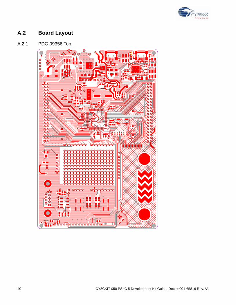
A.2 Board Layout
A.2.1 PDC-09356 Top
CY8CKIT-050 PSoC 5 Development Kit Guide, Doc. # 001-65816 Rev. *A 41
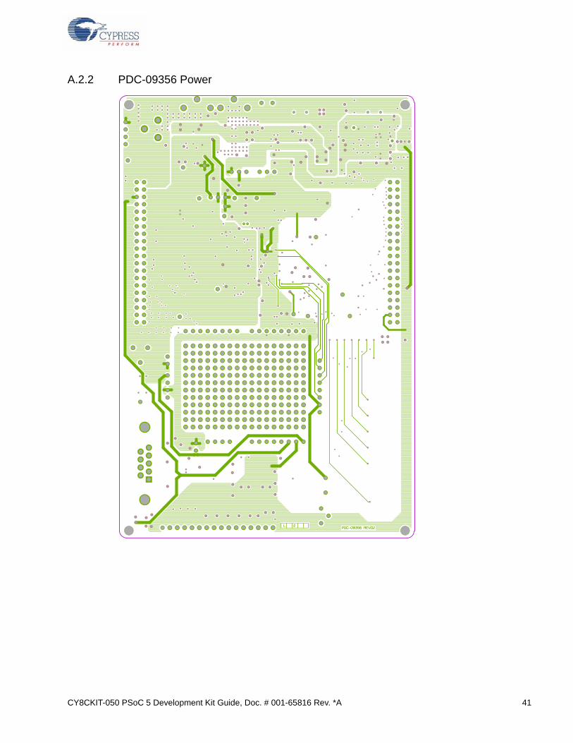
A.2.2 PDC-09356 Power
42 CY8CKIT-050 PSoC 5 Development Kit Guide, Doc. # 001-65816 Rev. *A
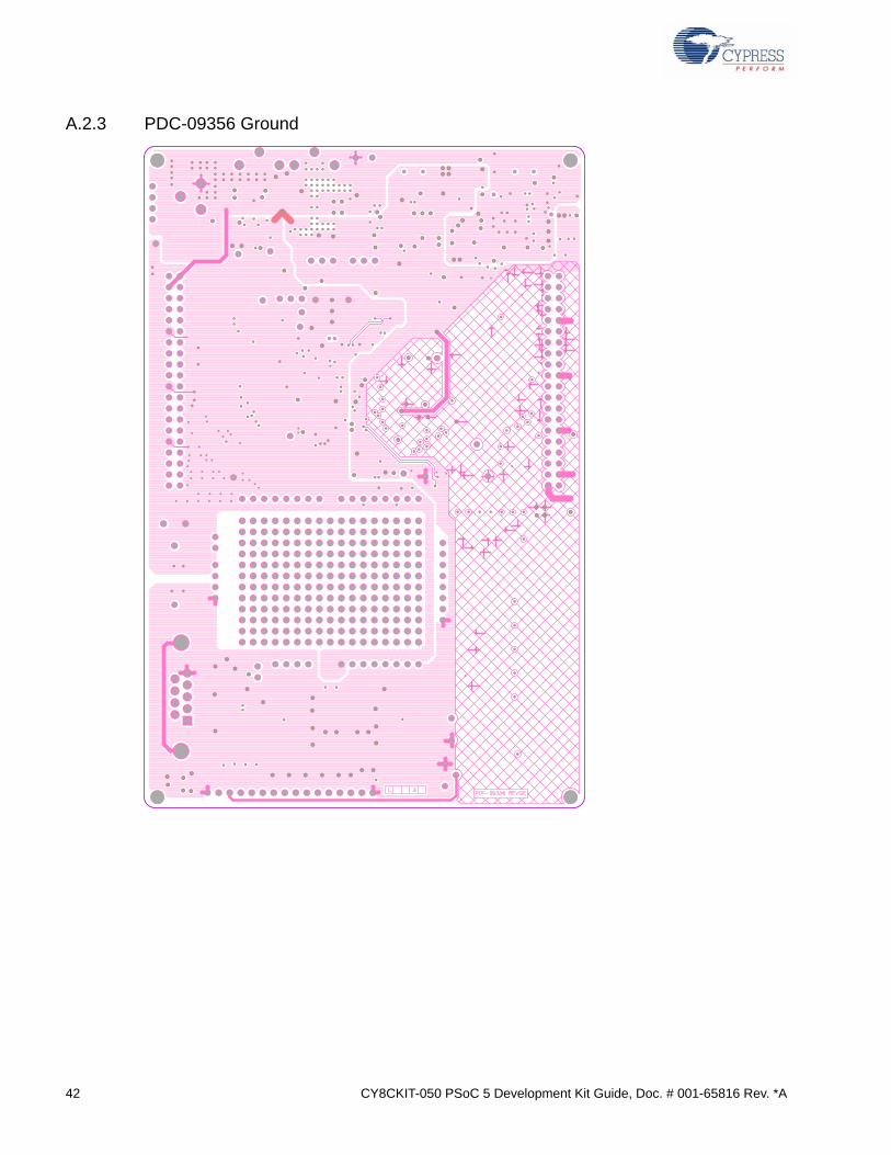
A.2.3 PDC-09356 Ground
CY8CKIT-050 PSoC 5 Development Kit Guide, Doc. # 001-65816 Rev. *A 43
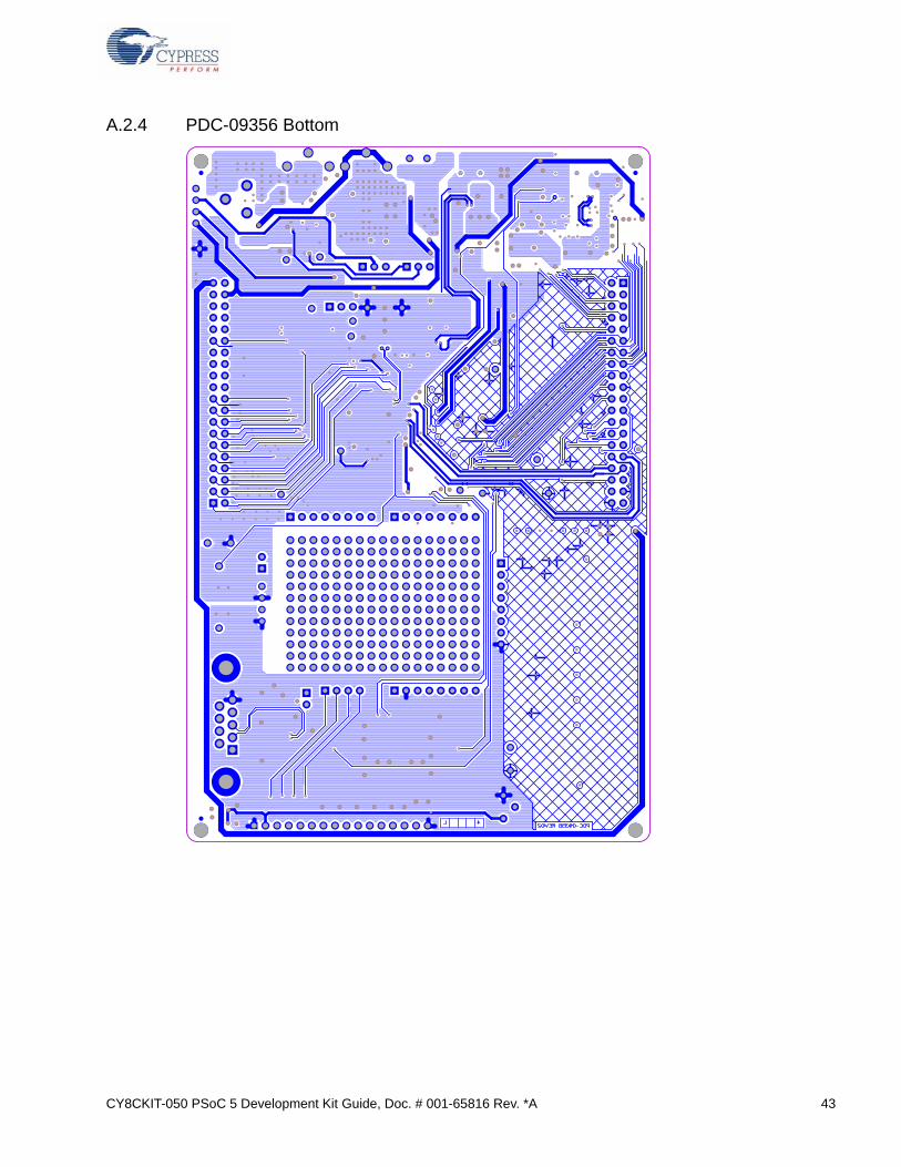
A.2.4 PDC-09356 Bottom
44 CY8CKIT-050 PSoC 5 Development Kit Guide, Doc. # 001-65816 Rev. *A
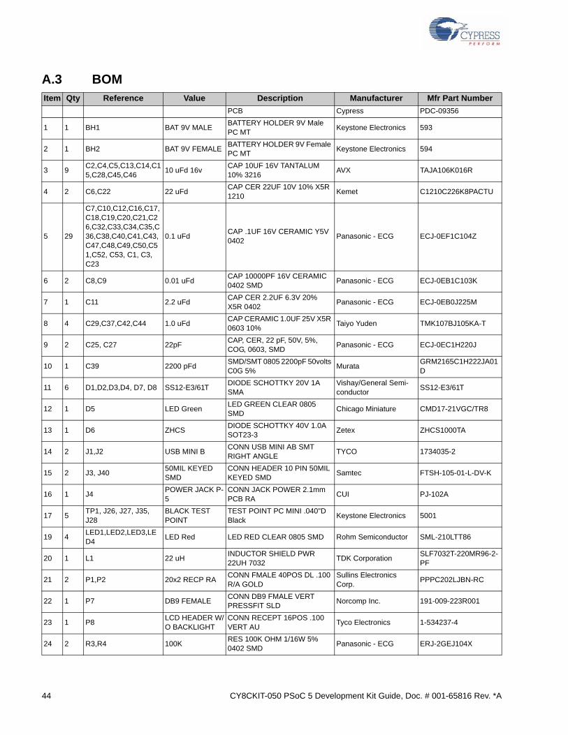
A.3 BOM Item Qty Reference Value Description Manufacturer Mfr Part Number
PCB Cypress PDC-09356
1 1 BH1 BAT 9V MALEBATTERY HOLDER 9V Male PC MT
Keystone Electronics 593
2 1 BH2 BAT 9V FEMALEBATTERY HOLDER 9V Female PC MT
Keystone Electronics 594
3 9C2,C4,C5,C13,C14,C15,C28,C45,C46
10 uFd 16vCAP 10UF 16V TANTALUM 10% 3216
AVX TAJA106K016R
4 2 C6,C22 22 uFdCAP CER 22UF 10V 10% X5R 1210
Kemet C1210C226K8PACTU
5 29
C7,C10,C12,C16,C17,C18,C19,C20,C21,C26,C32,C33,C34,C35,C36,C38,C40,C41,C43,C47,C48,C49,C50,C51,C52, C53, C1, C3, C23
0.1 uFdCAP .1UF 16V CERAMIC Y5V 0402
Panasonic - ECG ECJ-0EF1C104Z
6 2 C8,C9 0.01 uFdCAP 10000PF 16V CERAMIC 0402 SMD
Panasonic - ECG ECJ-0EB1C103K
7 1 C11 2.2 uFdCAP CER 2.2UF 6.3V 20% X5R 0402
Panasonic - ECG ECJ-0EB0J225M
8 4 C29,C37,C42,C44 1.0 uFdCAP CERAMIC 1.0UF 25V X5R 0603 10%
Taiyo Yuden TMK107BJ105KA-T
9 2 C25, C27 22pFCAP, CER, 22 pF, 50V, 5%, COG, 0603, SMD
Panasonic - ECG ECJ-0EC1H220J
10 1 C39 2200 pFdSMD/SMT 0805 2200pF 50volts C0G 5%
MurataGRM2165C1H222JA01D
11 6 D1,D2,D3,D4, D7, D8 SS12-E3/61TDIODE SCHOTTKY 20V 1A SMA
Vishay/General Semi-conductor
SS12-E3/61T
12 1 D5 LED GreenLED GREEN CLEAR 0805 SMD
Chicago Miniature CMD17-21VGC/TR8
13 1 D6 ZHCSDIODE SCHOTTKY 40V 1.0A SOT23-3
Zetex ZHCS1000TA
14 2 J1,J2 USB MINI BCONN USB MINI AB SMT RIGHT ANGLE
TYCO 1734035-2
15 2 J3, J4050MIL KEYED SMD
CONN HEADER 10 PIN 50MIL KEYED SMD
Samtec FTSH-105-01-L-DV-K
16 1 J4POWER JACK P-5
CONN JACK POWER 2.1mm PCB RA
CUI PJ-102A
17 5TP1, J26, J27, J35, J28
BLACK TEST POINT
TEST POINT PC MINI .040"D Black
Keystone Electronics 5001
19 4LED1,LED2,LED3,LED4
LED Red LED RED CLEAR 0805 SMD Rohm Semiconductor SML-210LTT86
20 1 L1 22 uHINDUCTOR SHIELD PWR 22UH 7032
TDK CorporationSLF7032T-220MR96-2-PF
21 2 P1,P2 20x2 RECP RACONN FMALE 40POS DL .100 R/A GOLD
Sullins Electronics Corp.
PPPC202LJBN-RC
22 1 P7 DB9 FEMALECONN DB9 FMALE VERT PRESSFIT SLD
Norcomp Inc. 191-009-223R001
23 1 P8LCD HEADER W/O BACKLIGHT
CONN RECEPT 16POS .100 VERT AU
Tyco Electronics 1-534237-4
24 2 R3,R4 100KRES 100K OHM 1/16W 5% 0402 SMD
Panasonic - ECG ERJ-2GEJ104X
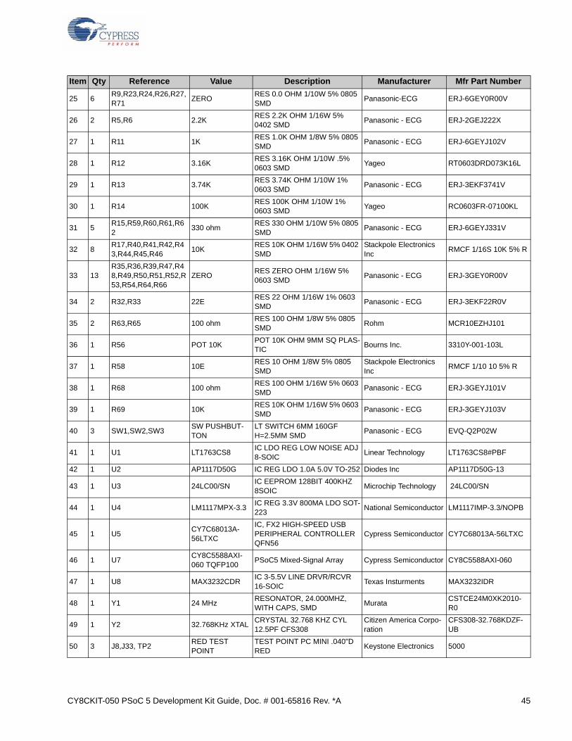
CY8CKIT-050 PSoC 5 Development Kit Guide, Doc. # 001-65816 Rev. *A 45
25 6R9,R23,R24,R26,R27,R71
ZERORES 0.0 OHM 1/10W 5% 0805 SMD
Panasonic-ECG ERJ-6GEY0R00V
26 2 R5,R6 2.2KRES 2.2K OHM 1/16W 5% 0402 SMD
Panasonic - ECG ERJ-2GEJ222X
27 1 R11 1KRES 1.0K OHM 1/8W 5% 0805 SMD
Panasonic - ECG ERJ-6GEYJ102V
28 1 R12 3.16KRES 3.16K OHM 1/10W .5% 0603 SMD
Yageo RT0603DRD073K16L
29 1 R13 3.74KRES 3.74K OHM 1/10W 1% 0603 SMD
Panasonic - ECG ERJ-3EKF3741V
30 1 R14 100KRES 100K OHM 1/10W 1% 0603 SMD
Yageo RC0603FR-07100KL
31 5R15,R59,R60,R61,R62
330 ohmRES 330 OHM 1/10W 5% 0805 SMD
Panasonic - ECG ERJ-6GEYJ331V
32 8R17,R40,R41,R42,R43,R44,R45,R46
10KRES 10K OHM 1/16W 5% 0402 SMD
Stackpole Electronics Inc
RMCF 1/16S 10K 5% R
33 13R35,R36,R39,R47,R48,R49,R50,R51,R52,R53,R54,R64,R66
ZERORES ZERO OHM 1/16W 5% 0603 SMD
Panasonic - ECG ERJ-3GEY0R00V
34 2 R32,R33 22ERES 22 OHM 1/16W 1% 0603 SMD
Panasonic - ECG ERJ-3EKF22R0V
35 2 R63,R65 100 ohmRES 100 OHM 1/8W 5% 0805 SMD
Rohm MCR10EZHJ101
36 1 R56 POT 10KPOT 10K OHM 9MM SQ PLAS-TIC
Bourns Inc. 3310Y-001-103L
37 1 R58 10ERES 10 OHM 1/8W 5% 0805 SMD
Stackpole Electronics Inc
RMCF 1/10 10 5% R
38 1 R68 100 ohmRES 100 OHM 1/16W 5% 0603 SMD
Panasonic - ECG ERJ-3GEYJ101V
39 1 R69 10KRES 10K OHM 1/16W 5% 0603 SMD
Panasonic - ECG ERJ-3GEYJ103V
40 3 SW1,SW2,SW3SW PUSHBUT-TON
LT SWITCH 6MM 160GF H=2.5MM SMD
Panasonic - ECG EVQ-Q2P02W
41 1 U1 LT1763CS8IC LDO REG LOW NOISE ADJ 8-SOIC
Linear Technology LT1763CS8#PBF
42 1 U2 AP1117D50G IC REG LDO 1.0A 5.0V TO-252 Diodes Inc AP1117D50G-13
43 1 U3 24LC00/SNIC EEPROM 128BIT 400KHZ 8SOIC
Microchip Technology 24LC00/SN
44 1 U4 LM1117MPX-3.3IC REG 3.3V 800MA LDO SOT-223
National Semiconductor LM1117IMP-3.3/NOPB
45 1 U5CY7C68013A-56LTXC
IC, FX2 HIGH-SPEED USB PERIPHERAL CONTROLLER QFN56
Cypress Semiconductor CY7C68013A-56LTXC
46 1 U7CY8C5588AXI-060 TQFP100
PSoC5 Mixed-Signal Array Cypress Semiconductor CY8C5588AXI-060
47 1 U8 MAX3232CDRIC 3-5.5V LINE DRVR/RCVR 16-SOIC
Texas Insturments MAX3232IDR
48 1 Y1 24 MHzRESONATOR, 24.000MHZ, WITH CAPS, SMD
MurataCSTCE24M0XK2010-R0
49 1 Y2 32.768KHz XTALCRYSTAL 32.768 KHZ CYL 12.5PF CFS308
Citizen America Corpo-ration
CFS308-32.768KDZF-UB
50 3 J8,J33, TP2RED TEST POINT
TEST POINT PC MINI .040"D RED
Keystone Electronics 5000
Item Qty Reference Value Description Manufacturer Mfr Part Number
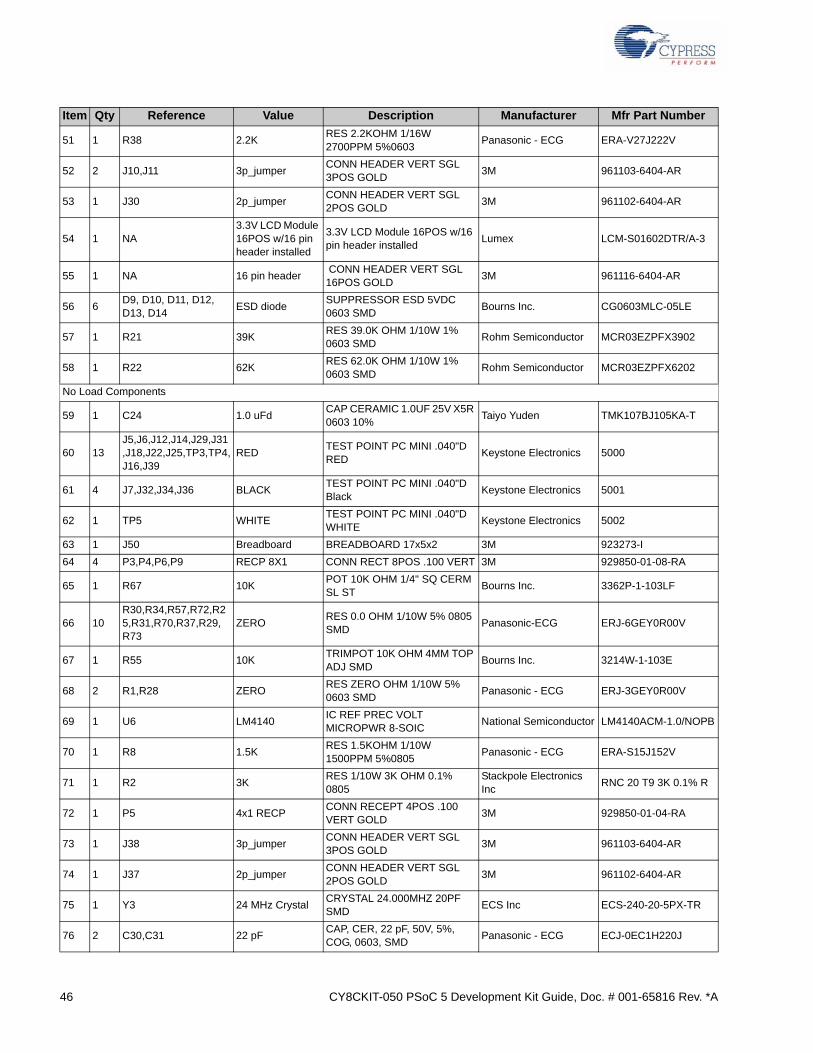
46 CY8CKIT-050 PSoC 5 Development Kit Guide, Doc. # 001-65816 Rev. *A
51 1 R38 2.2KRES 2.2KOHM 1/16W 2700PPM 5%0603
Panasonic - ECG ERA-V27J222V
52 2 J10,J11 3p_jumperCONN HEADER VERT SGL 3POS GOLD
3M 961103-6404-AR
53 1 J30 2p_jumperCONN HEADER VERT SGL 2POS GOLD
3M 961102-6404-AR
54 1 NA3.3V LCD Module 16POS w/16 pin header installed
3.3V LCD Module 16POS w/16 pin header installed
Lumex LCM-S01602DTR/A-3
55 1 NA 16 pin header CONN HEADER VERT SGL 16POS GOLD
3M 961116-6404-AR
56 6D9, D10, D11, D12, D13, D14
ESD diodeSUPPRESSOR ESD 5VDC 0603 SMD
Bourns Inc. CG0603MLC-05LE
57 1 R21 39KRES 39.0K OHM 1/10W 1% 0603 SMD
Rohm Semiconductor MCR03EZPFX3902
58 1 R22 62KRES 62.0K OHM 1/10W 1% 0603 SMD
Rohm Semiconductor MCR03EZPFX6202
No Load Components
59 1 C24 1.0 uFdCAP CERAMIC 1.0UF 25V X5R 0603 10%
Taiyo Yuden TMK107BJ105KA-T
60 13J5,J6,J12,J14,J29,J31,J18,J22,J25,TP3,TP4,J16,J39
REDTEST POINT PC MINI .040"D RED
Keystone Electronics 5000
61 4 J7,J32,J34,J36 BLACKTEST POINT PC MINI .040"D Black
Keystone Electronics 5001
62 1 TP5 WHITETEST POINT PC MINI .040"D WHITE
Keystone Electronics 5002
63 1 J50 Breadboard BREADBOARD 17x5x2 3M 923273-I
64 4 P3,P4,P6,P9 RECP 8X1 CONN RECT 8POS .100 VERT 3M 929850-01-08-RA
65 1 R67 10KPOT 10K OHM 1/4" SQ CERM SL ST
Bourns Inc. 3362P-1-103LF
66 10R30,R34,R57,R72,R25,R31,R70,R37,R29, R73
ZERORES 0.0 OHM 1/10W 5% 0805 SMD
Panasonic-ECG ERJ-6GEY0R00V
67 1 R55 10KTRIMPOT 10K OHM 4MM TOP ADJ SMD
Bourns Inc. 3214W-1-103E
68 2 R1,R28 ZERORES ZERO OHM 1/10W 5% 0603 SMD
Panasonic - ECG ERJ-3GEY0R00V
69 1 U6 LM4140IC REF PREC VOLT MICROPWR 8-SOIC
National Semiconductor LM4140ACM-1.0/NOPB
70 1 R8 1.5KRES 1.5KOHM 1/10W 1500PPM 5%0805
Panasonic - ECG ERA-S15J152V
71 1 R2 3KRES 1/10W 3K OHM 0.1% 0805
Stackpole Electronics Inc
RNC 20 T9 3K 0.1% R
72 1 P5 4x1 RECPCONN RECEPT 4POS .100 VERT GOLD
3M 929850-01-04-RA
73 1 J38 3p_jumperCONN HEADER VERT SGL 3POS GOLD
3M 961103-6404-AR
74 1 J37 2p_jumperCONN HEADER VERT SGL 2POS GOLD
3M 961102-6404-AR
75 1 Y3 24 MHz CrystalCRYSTAL 24.000MHZ 20PF SMD
ECS Inc ECS-240-20-5PX-TR
76 2 C30,C31 22 pFCAP, CER, 22 pF, 50V, 5%, COG, 0603, SMD
Panasonic - ECG ECJ-0EC1H220J
Item Qty Reference Value Description Manufacturer Mfr Part Number
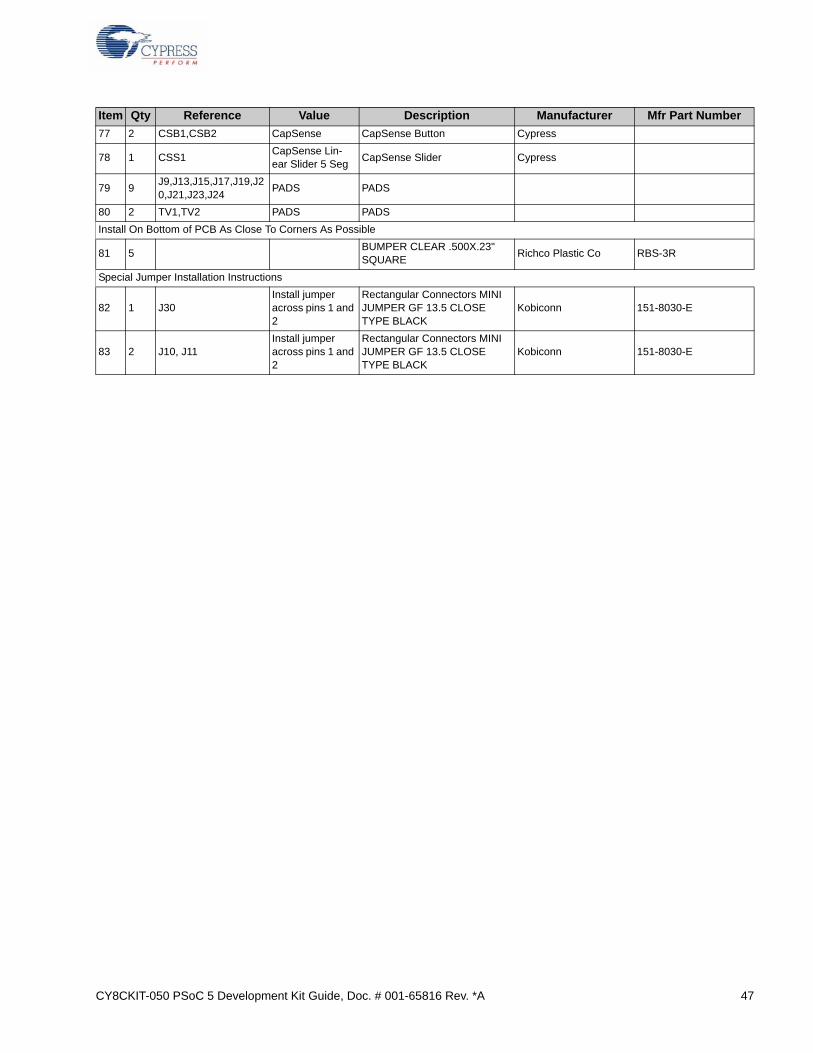
CY8CKIT-050 PSoC 5 Development Kit Guide, Doc. # 001-65816 Rev. *A 47
77 2 CSB1,CSB2 CapSense CapSense Button Cypress
78 1 CSS1CapSense Lin-ear Slider 5 Seg
CapSense Slider Cypress
79 9J9,J13,J15,J17,J19,J20,J21,J23,J24
PADS PADS
80 2 TV1,TV2 PADS PADS
Install On Bottom of PCB As Close To Corners As Possible
81 5BUMPER CLEAR .500X.23" SQUARE
Richco Plastic Co RBS-3R
Special Jumper Installation Instructions
82 1 J30Install jumper across pins 1 and 2
Rectangular Connectors MINI JUMPER GF 13.5 CLOSE TYPE BLACK
Kobiconn 151-8030-E
83 2 J10, J11Install jumper across pins 1 and 2
Rectangular Connectors MINI JUMPER GF 13.5 CLOSE TYPE BLACK
Kobiconn 151-8030-E
Item Qty Reference Value Description Manufacturer Mfr Part Number

48 CY8CKIT-050 PSoC 5 Development Kit Guide, Doc. # 001-65816 Rev. *A