Embed Size (px)
Citation preview
CY8C20x37/37S/47/47S/67/67S
1.8 V CapSense® Controller with SmartSense™ Auto-tuning –
31 Buttons, 6 Sliders
Cypress Semiconductor Corporation • 198 Champion Court • San Jose, CA 95134-1709 • 408-943-2600Document Number: 001-69257 Rev. *F Revised July 3, 2012
1.8 V CapSense® Controller with SmartSense™ Auto-tuning Support
Features
■ QuietZone™ Controller❐ Patented Capacitive Sigma Delta PLUS (CSD PLUS™)
sensing algorithm for robust performance❐ High Sensitivity (0.1 pF) and best-in-class SNR performance
to support:• Ideal for proximity solutions• Overlay thickness of 15 mm for glass and 5 mm plastic
❐ Superior noise immunity performance against conducted and radiated noise and ultra low radiated emissions• Reliable and robust touch performance in noisy environ-
ments❐ Standardized user modules for overcoming noise
■ Low power CapSense® block with SmartSense™ auto-tuning❐ Supports a combination of up to 31 buttons or 6 sliders, prox-
imity sensors❐ Low average power consumption - 28 A for each sensor at
runtime (wake from sleep and scan sensors every 125 ms)❐ SmartSense auto-tuning
• Sets and maintains optimal sensor performance during runtime
• Eliminates system tuning during development and produc-tion
• Compensates for variations in manufacturing process
■ Driven shield available on five GPIO pins❐ Max load of 100 pF at 3 MHz ❐ Frequency range: 375 kHz to 3 MHz❐ Delivers best-in class water tolerant designs❐ Robust proximity sensing in the presence of metal objects
■ Powerful Harvard-architecture processor❐ M8C CPU with a maximum speed of 24 MHz❐ Operating range: 1.71 V to 5.5 V
• Standby mode: 1.1 µA (typ)• Deep sleep: 0.1 µA (typ)
❐ Temperature range: –40 °C to +85 °C
■ Flexible on-chip memory❐ 8 KB flash, 1 KB SRAM❐ 16 KB flash, 2 KB SRAM❐ 32 KB flash, 2 KB SRAM❐ 50,000 flash erase/write cycles❐ In-system programming capability
■ Four clock sources❐ Internal main oscillator (IMO): 6/12/24 MHz
❐ Internal low-speed oscillator (ILO) at 32 kHz for watchdog and sleep timers
❐ RC crystal oscillator❐ Clock input
■ Programmable pin configurations❐ Up to 32 general-purpose I/Os (GPIOs)❐ Dual mode GPIO❐ High sink current of 25 mA for each GPIO. Total 120 mA
maximum sink current per chip❐ 5 mA source current on port 0 and 1 and 1 mA on port 2,3
and 4❐ Configurable internal pull-up, high-Z, and open drain modes❐ Selectable, regulated digital I/O on port 1❐ Configurable input threshold on port 1
■ Versatile analog mux❐ Common internal analog bus❐ Simultaneous connection of I/O❐ High power supply rejection ratio (PSRR) comparator❐ Low-dropout voltage regulator for all analog resources
■ Additional system resources❐ I2C slave:
• Selectable to 50 kHz, 100 kHz, or 400 kHz• Selectable clock stretch or forced Nack mode• Implementation during sleep modes with less than 100 µA• I2C wake from sleep with hardware address validation
❐ 12 MHz SPI master and slave❐ Three 16-bit timers❐ Watchdog and sleep timers❐ Internal voltage reference❐ Integrated supervisory circuit❐ 10-bit incremental analog-to-digital converter (ADC)❐ Two general-purpose high speed, low power analog compar-
ators
■ Complete development tools❐ Free development tool (PSoC Designer™)
■ Package options❐ 16-pin SOIC (150 mil)❐ 16-pin QFN – 3 × 3 × 0.6 mm❐ 24-pin QFN – 4 × 4 × 0.6 mm❐ 32-pin QFN – 5 × 5 × 0.6 mm❐ 48-pin QFN – 6 × 6 × 0.6 mm❐ 30-ball WLCSP[1]
Note1. Contact your nearest Cypress sales office for details.
CY8C20x37/37S/47/47S/67/67S
Document Number: 001-69257 Rev. *F Page 2 of 39
Logic Block Diagram
CAPSENSE SYSTEM
1K/2 K SRAM
InterruptController
Sleep and Watchdog
Multiple Clock Sources
Internal Low Speed Oscillator ( ILO)6/12/ 24 MHz Internal Main Oscillator
( IMO)
PSoC CORE
CPU Core (M8C)
Supervisory ROM (SROM)8K/16K/32 K Flash Nonvolatile Memory
SYSTEM RESOURCES
SYSTEM BUS
AnalogReference
SYSTEM BUS
Port 3 Port 2 Port 1 Port 0
CapSense Module
Global Analog Interconnect
1.8/2.5/3 V LDO
Analog Mux
I2CSlave
SPIMaster/Slave
PORandLVD
SystemResets
Internal Voltage
References
Three 16- Bit Programmable
Timers
PWRSYS(Regulator)
Port 4
Digital Clocks
Comparator #2
Comparator #1
[2]
Note2. Internal voltage regulator for internal circuitry
CY8C20x37/37S/47/47S/67/67S
Document Number: 001-69257 Rev. *F Page 3 of 39
Contents
PSoC® Functional Overview ............................................ 4PSoC Core .................................................................. 4CapSense System ....................................................... 4Additional System Resources ..................................... 5
Getting Started .................................................................. 5Application Notes/Design Guides ................................ 5Development Kits ........................................................ 5Training .......................................................................5CYPros Consultants .................................................... 5Solutions Library .......................................................... 5Technical Support ....................................................... 5
Designing with PSoC Designer ....................................... 6Select Components ..................................................... 6Configure Components ............................................... 6Organize and Connect ................................................ 6Generate, Verify, and Debug ....................................... 6
Pinouts .............................................................................. 716-pin SOIC (12 Sensing Inputs) ................................ 716-pin QFN (12 Sensing Inputs) .................................. 824-pin QFN (20 Sensing Inputs) .................................. 930-ball WLCSP (26 Sensing Inputs) .......................... 1032-pin QFN (26 Sensing Inputs) ................................ 1148-pin QFN (33 Sensing Inputs) ................................ 12
Electrical Specifications ................................................ 13Absolute Maximum Ratings ....................................... 13Operating Temperature ............................................. 13DC Chip-Level Specifications .................................... 14DC GPIO Specifications ............................................ 15DC Analog Mux Bus Specifications ........................... 17DC Low Power Comparator Specifications ............... 17Comparator User Module Electrical Specifications ... 18ADC Electrical Specifications .................................... 18DC POR and LVD Specifications .............................. 19DC Programming Specifications ............................... 19DC I2C Specifications ............................................... 20Shield Driver DC Specifications ................................ 20
DC IDAC Specifications ............................................ 20AC Chip-Level Specifications .................................... 21AC General Purpose I/O Specifications .................... 22AC Comparator Specifications .................................. 22AC External Clock Specifications .............................. 22AC Programming Specifications ................................ 23AC I2C Specifications ................................................ 24
Packaging Information ................................................... 27Thermal Impedances ................................................. 30Capacitance on Crystal Pins ..................................... 30Solder Reflow Peak Temperature ............................. 30
Development Tool Selection ......................................... 31Software .................................................................... 31Development Kits ...................................................... 31Evaluation Tools ........................................................ 31Device Programmers ................................................. 31Accessories (Emulation and Programming) .............. 32Third Party Tools ....................................................... 32Build a PSoC Emulator into Your Board .................... 32
Ordering Information ...................................................... 33Ordering Code Definitions ......................................... 34
Acronyms ........................................................................ 35Reference Documents .................................................... 35
Document Conventions ............................................. 35Units of Measure ....................................................... 35Numeric Naming ........................................................ 36
Glossary .......................................................................... 36Document History Page ................................................. 37Sales, Solutions, and Legal Information ...................... 39
Worldwide Sales and Design Support ....................... 39Products .................................................................... 39PSoC Solutions ......................................................... 39
CY8C20x37/37S/47/47S/67/67S
Document Number: 001-69257 Rev. *F Page 4 of 39
PSoC® Functional Overview
The PSoC family consists of many devices with on-chipcontrollers. These devices are designed to replace multipletraditional MCU-based system components with one low-costsingle-chip programmable component. A PSoC device includesconfigurable blocks of analog and digital logic, andprogrammable interconnect. This architecture makes it possiblefor you to create customized peripheral configurations, to matchthe requirements of each individual application. Additionally, afast central processing unit (CPU), flash program memory,SRAM data memory, and configurable I/O are included in arange of convenient pinouts.
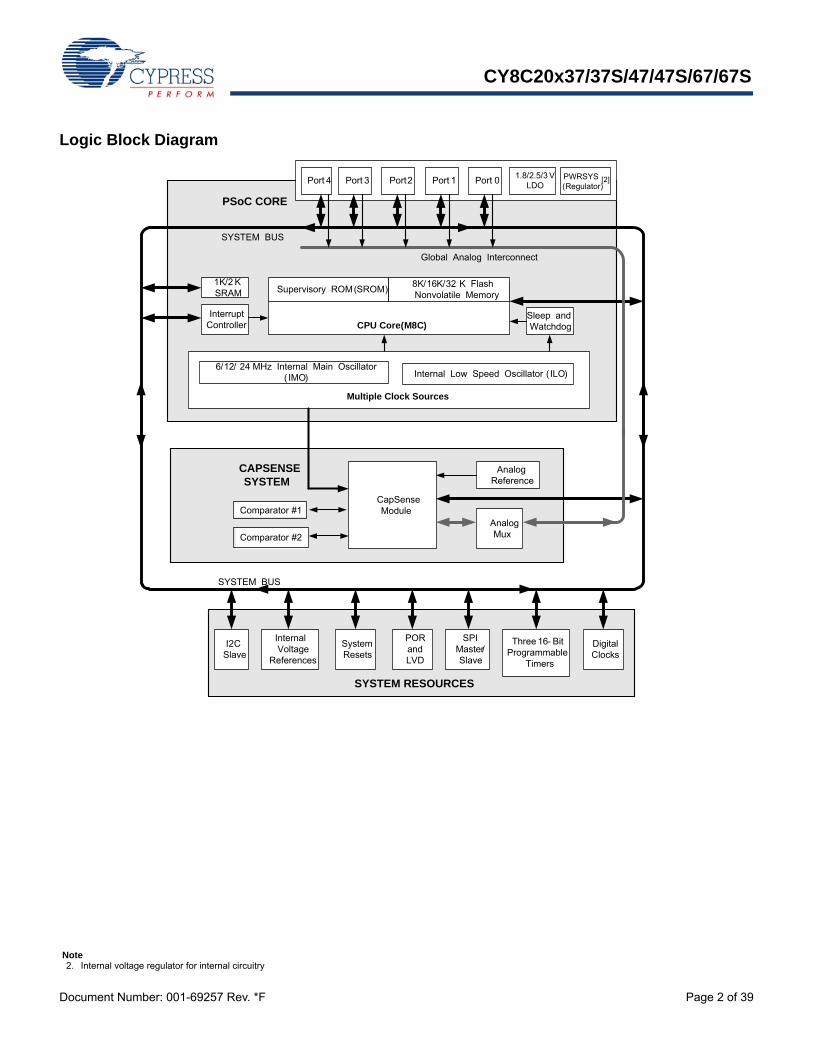
The architecture for this device family, as shown in the LogicBlock Diagram on page 2, consists of three main areas:
■ The core
■ CapSense analog system
■ System resources
A common, versatile bus allows connection between I/O and theanalog system.
Each CY8C20x37/47/67/S PSoC device includes a dedicatedCapSense block that provides sensing and scanning controlcircuitry for capacitive sensing applications. Depending on thePSoC package, up to 34 GPIOs are also included. The GPIOsprovide access to the MCU and analog mux.
PSoC Core
The PSoC core is a powerful engine that supports a richinstruction set. It encompasses SRAM for data storage, aninterrupt controller, sleep and watchdog timers, and IMO andILO. The CPU core, called the M8C, is a powerful processor withspeeds up to 24 MHz. The M8C is a 4-million instructions persecond (MIPS), 8-bit Harvard-architecture microprocessor.
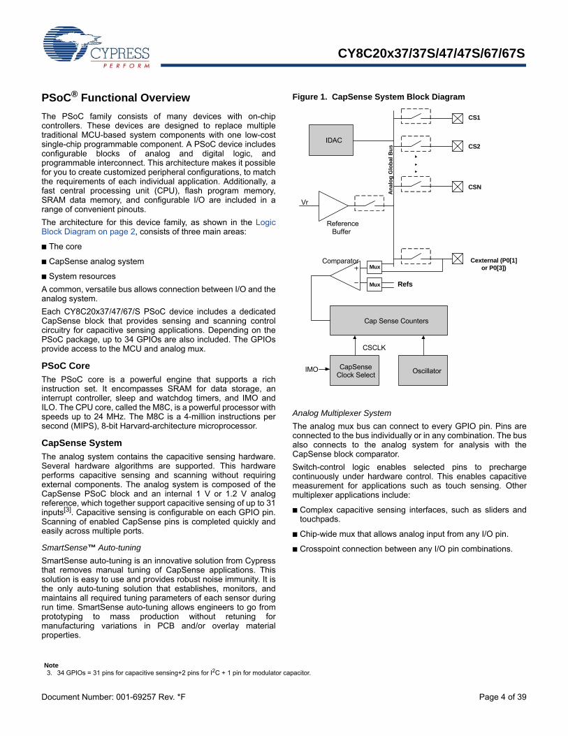
CapSense System
The analog system contains the capacitive sensing hardware.Several hardware algorithms are supported. This hardwareperforms capacitive sensing and scanning without requiringexternal components. The analog system is composed of theCapSense PSoC block and an internal 1 V or 1.2 V analogreference, which together support capacitive sensing of up to 31inputs[3]. Capacitive sensing is configurable on each GPIO pin.Scanning of enabled CapSense pins is completed quickly andeasily across multiple ports.
SmartSense™ Auto-tuning
SmartSense auto-tuning is an innovative solution from Cypressthat removes manual tuning of CapSense applications. Thissolution is easy to use and provides robust noise immunity. It isthe only auto-tuning solution that establishes, monitors, andmaintains all required tuning parameters of each sensor duringrun time. SmartSense auto-tuning allows engineers to go fromprototyping to mass production without retuning formanufacturing variations in PCB and/or overlay materialproperties.
Figure 1. CapSense System Block Diagram
Analog Multiplexer System
The analog mux bus can connect to every GPIO pin. Pins areconnected to the bus individually or in any combination. The busalso connects to the analog system for analysis with theCapSense block comparator.
Switch-control logic enables selected pins to prechargecontinuously under hardware control. This enables capacitivemeasurement for applications such as touch sensing. Othermultiplexer applications include:
■ Complex capacitive sensing interfaces, such as sliders andtouchpads.
■ Chip-wide mux that allows analog input from any I/O pin.
■ Crosspoint connection between any I/O pin combinations.
IDAC
ReferenceBuffer
Vr
An
alo
g G
lob
al B
us
Cap Sense Counters
ComparatorMux
Mux Refs
CapSenseClock Select
Oscillator
CSCLK
IMO
CS1
CS2
CSN
Cexternal (P0[1] or P0[3])
Note3. 34 GPIOs = 31 pins for capacitive sensing+2 pins for I2C + 1 pin for modulator capacitor.
CY8C20x37/37S/47/47S/67/67S
Document Number: 001-69257 Rev. *F Page 5 of 39
Additional System Resources
System resources provide additional capability, such asconfigurable I2C slave, SPI master/slave communicationinterface, three 16-bit programmable timers, various systemresets supported by the M8C low voltage detection and power-on reset. The merits of each system resource are listed here:
■ The I2C slave/SPI master-slave module provides 50/100/400 kHz communication over two wires. SPI communicationover three or four wires runs at speeds of 46.9 kHz to 3 MHz(lower for a slower system clock).
■ The I2C hardware address recognition feature reduces thealready low power consumption by eliminating the need forCPU intervention until a packet addressed to the target deviceis received.
■ The I2C enhanced slave interface appears as a 32-byte RAMbuffer to the external I2C master. Using a simple predefinedprotocol, the master controls the read and write pointers intothe RAM. When this method is enabled, the slave does not stallthe bus when receiving data bytes in active mode. For usagedetails, see the application note I2C Enhanced Slave Operation- AN56007.
■ Low-voltage detection (LVD) interrupts can signal theapplication of falling voltage levels, while the advanced power-on reset (POR) circuit eliminates the need for a systemsupervisor.
■ An internal reference provides an absolute reference forcapacitive sensing.
■ A register-controlled bypass mode allows the user to disablethe LDO regulator.
Getting Started
The quickest way to understand PSoC silicon is to read thisdatasheet and then use the PSoC Designer IntegratedDevelopment Environment (IDE). This datasheet is an overviewof the PSoC integrated circuit and presents specific pin, register,and electrical specifications.
For in depth information, along with detailed programmingdetails, see the Technical Reference Manual for the CY8C20x37/47/67/S PSoC devices.
For up-to-date ordering, packaging, and electrical specificationinformation, see the latest PSoC device datasheets on the webat www.cypress.com/psoc.
Application Notes/Design Guides
Application notes and design guides are an excellentintroduction to the wide variety of possible PSoC designs. Theyare located at www.cypress.com/gocapsense. SelectApplication Notes under the Related Documentation tab.
Development Kits
PSoC Development Kits are available online from Cypress atwww.cypress.com/shop and through a growing number ofregional and global distributors, which include Arrow, Avnet, Digi-Key, Farnell, Future Electronics, and Newark. See DevelopmentKits on page 31.
Training
Free PSoC and CapSense technical training (on demand,webinars, and workshops) is available online atwww.cypress.com/training. The training covers a wide variety oftopics and skill levels to assist you in your designs.
CYPros Consultants
Certified PSoC Consultants offer everything from technicalassistance to completed PSoC designs. To contact or become aPSoC Consultant go to www.cypress.com/cypros.
Solutions Library
Visit our growing library of solution focused designs atwww.cypress.com/solutions. Here you can find variousapplication designs that include firmware and hardware designfiles that enable you to complete your designs quickly.
Technical Support
For assistance with technical issues, search KnowledgeBasearticles and forums at www.cypress.com/support. If you cannotfind an answer to your question, create a technical support caseor call technical support at 1-800-541-4736.
CY8C20x37/37S/47/47S/67/67S
Document Number: 001-69257 Rev. *F Page 6 of 39
Designing with PSoC DesignerThe PSoC development process can be summarized in thefollowing four steps:
1. Select User Modules
2. Configure User Modules
3. Organize and Connect
4. Generate and Verify
Select Components
PSoC Designer provides a library of pre-built, pre-testedhardware peripheral components called “user modules”. Usermodules make selecting and implementing peripheral devices,both analog and digital, simple.
Configure Components
Each of the User Modules you select establishes the basicregister settings that implement the selected function. They alsoprovide parameters and properties that allow you to tailor theirprecise configuration to your particular application. The usermodule parameters permit you to establish the pulse width andduty cycle. Configure the parameters and properties tocorrespond to your chosen application. Enter values directly orby selecting values from drop-down menus. All the user modulesare documented in datasheets that may be viewed directly inPSoC Designer or on the Cypress website. These user moduledatasheets explain the internal operation of the User Module andprovide performance specifications. Each datasheet describesthe use of each user module parameter, and other informationyou may need to successfully implement your design.
Organize and Connect
You build signal chains at the chip level by interconnecting usermodules to each other and the I/O pins. You perform theselection, configuration, and routing so that you have completecontrol over all on-chip resources.
Generate, Verify, and Debug
When you are ready to test the hardware configuration or moveon to developing code for the project, you perform the “GenerateConfiguration Files” step. This causes PSoC Designer togenerate source code that automatically configures the device toyour specification and provides the software for the system. Thegenerated code provides application programming interfaces(APIs) with high-level functions to control and respond tohardware events at run time and interrupt service routines thatyou can adapt as needed.
A complete code development environment allows you todevelop and customize your applications in C, assemblylanguage, or both.
CY8C20x37/37S/47/47S/67/67S
Document Number: 001-69257 Rev. *F Page 7 of 39
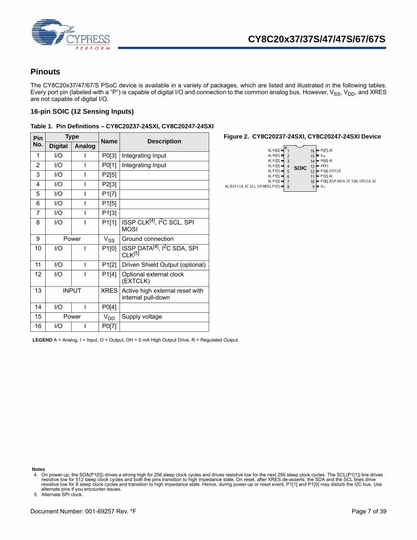
Pinouts
The CY8C20x37/47/67/S PSoC device is available in a variety of packages, which are listed and illustrated in the following tables.Every port pin (labeled with a “P”) is capable of digital I/O and connection to the common analog bus. However, VSS, VDD, and XRESare not capable of digital I/O.
16-pin SOIC (12 Sensing Inputs)
Table 1. Pin Definitions – CY8C20237-24SXI, CY8C20247-24SXI
Pin No.
TypeName Description
Figure 2. CY8C20237-24SXI, CY8C20247-24SXI Device
Digital Analog
1 I/O I P0[3] Integrating Input
2 I/O I P0[1] Integrating Input
3 I/O I P2[5]
4 I/O I P2[3]
5 I/O I P1[7]
6 I/O I P1[5]
7 I/O I P1[3]
8 I/O I P1[1] ISSP CLK[4], I2C SCL, SPI MOSI
9 Power VSS Ground connection
10 I/O I P1[0] ISSP DATA[4], I2C SDA, SPI CLK[5]
11 I/O I P1[2] Driven Shield Output (optional)
12 I/O I P1[4] Optional external clock (EXTCLK)
13 INPUT XRES Active high external reset with internal pull-down
14 I/O I P0[4]
15 Power VDD Supply voltage
16 I/O I P0[7]
LEGEND A = Analog, I = Input, O = Output, OH = 5 mA High Output Drive, R = Regulated Output.
SOIC
P0[7], AIVDD
P0[4], AIXRESP1[4], EXTCLKP1[2], AIP1[0], ISSP DATA, I2C SDA, SPI CLK, AIVSS
161514131211
12345678
AI, P0[3]AI, P0[1]AI, P2[5]AI, P2[3]AI, P1[7]AI, P1[5]AI, P1[3]
AI, ISSP CLK, I2C SCL, SPI MOSI, P1[1]10
9
Notes4. On power-up, the SDA(P1[0]) drives a strong high for 256 sleep clock cycles and drives resistive low for the next 256 sleep clock cycles. The SCL(P1[1]) line drives
resistive low for 512 sleep clock cycles and both the pins transition to high impedance state. On reset, after XRES de-asserts, the SDA and the SCL lines drive resistive low for 8 sleep clock cycles and transition to high impedance state. Hence, during power-up or reset event, P1[1] and P1[0] may disturb the I2C bus. Use alternate pins if you encounter issues.
5. Alternate SPI clock.
CY8C20x37/37S/47/47S/67/67S
Document Number: 001-69257 Rev. *F Page 8 of 39
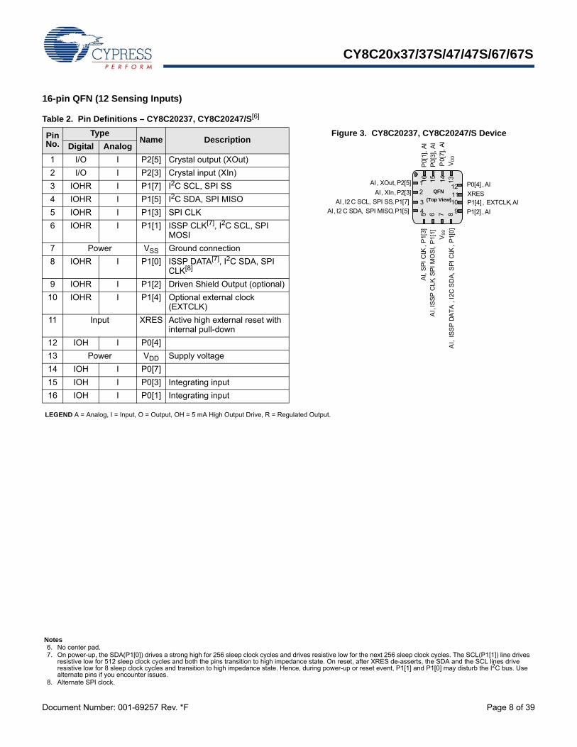
16-pin QFN (12 Sensing Inputs)
Table 2. Pin Definitions – CY8C20237, CY8C20247/S[6]
Pin No.
TypeName Description
Figure 3. CY8C20237, CY8C20247/S Device
Digital Analog
1 I/O I P2[5] Crystal output (XOut)
2 I/O I P2[3] Crystal input (XIn)
3 IOHR I P1[7] I2C SCL, SPI SS
4 IOHR I P1[5] I2C SDA, SPI MISO
5 IOHR I P1[3] SPI CLK
6 IOHR I P1[1] ISSP CLK[7], I2C SCL, SPI MOSI
7 Power VSS Ground connection
8 IOHR I P1[0] ISSP DATA[7], I2C SDA, SPI CLK[8]
9 IOHR I P1[2] Driven Shield Output (optional)
10 IOHR I P1[4] Optional external clock (EXTCLK)
11 Input XRES Active high external reset with internal pull-down
12 IOH I P0[4]
13 Power VDD Supply voltage
14 IOH I P0[7]
15 IOH I P0[3] Integrating input
16 IOH I P0[1] Integrating input
LEGEND A = Analog, I = Input, O = Output, OH = 5 mA High Output Drive, R = Regulated Output.
QFN
(Top View)
AI, XOut, P2[5]
AI , I2 C SCL, SPI SS, P1[7]
AI , I2 C SDA, SPI MISO, P1[5]
AI,
SP
I C
LK,
P1[
3]
12
34
11109
16
15
14
13
P0[
3],
AI
P0[
7],
AI
VD
D
P0[4] , AI
AI,
ISS
P C
LK,
SP
I M
OS
I, P
1[1]
AI,
IS
SP
DA
TA
, I2C
SD
A,
SP
I C
LK,
P1[
0]
P1[2] , AI
AI , XIn, P2[3]
P1[4] , EXTCLK, AIXRES
P0[
1],
AI
VS
S
12
5 6 7 8
Notes6. No center pad.7. On power-up, the SDA(P1[0]) drives a strong high for 256 sleep clock cycles and drives resistive low for the next 256 sleep clock cycles. The SCL(P1[1]) line drives
resistive low for 512 sleep clock cycles and both the pins transition to high impedance state. On reset, after XRES de-asserts, the SDA and the SCL lines drive resistive low for 8 sleep clock cycles and transition to high impedance state. Hence, during power-up or reset event, P1[1] and P1[0] may disturb the I2C bus. Use alternate pins if you encounter issues.
8. Alternate SPI clock.
CY8C20x37/37S/47/47S/67/67S
Document Number: 001-69257 Rev. *F Page 9 of 39
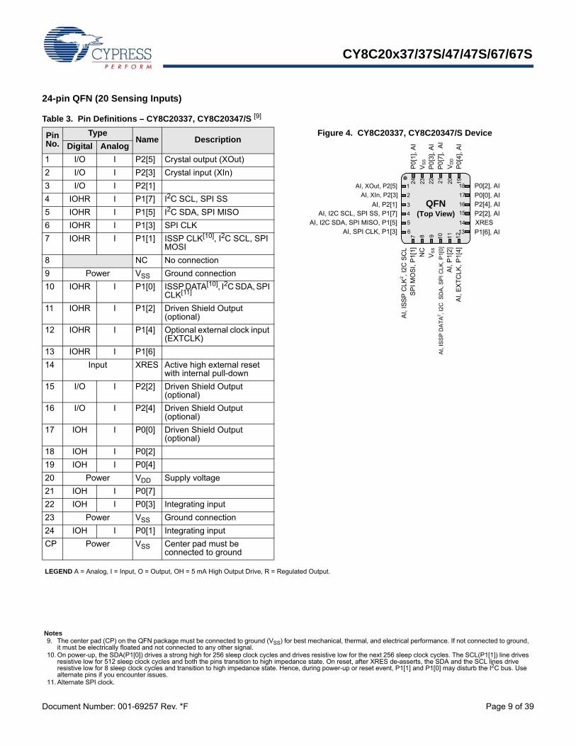
24-pin QFN (20 Sensing Inputs)
Table 3. Pin Definitions – CY8C20337, CY8C20347/S [9]
Pin No.
TypeName Description
Figure 4. CY8C20337, CY8C20347/S Device
Digital Analog
1 I/O I P2[5] Crystal output (XOut)
2 I/O I P2[3] Crystal input (XIn)
3 I/O I P2[1]
4 IOHR I P1[7] I2C SCL, SPI SS
5 IOHR I P1[5] I2C SDA, SPI MISO
6 IOHR I P1[3] SPI CLK
7 IOHR I P1[1] ISSP CLK[10], I2C SCL, SPI MOSI
8 NC No connection
9 Power VSS Ground connection
10 IOHR I P1[0] ISSP DATA[10], I2C SDA, SPI CLK[11]
11 IOHR I P1[2] Driven Shield Output (optional)
12 IOHR I P1[4] Optional external clock input (EXTCLK)
13 IOHR I P1[6]
14 Input XRES Active high external reset with internal pull-down
15 I/O I P2[2] Driven Shield Output (optional)
16 I/O I P2[4] Driven Shield Output (optional)
17 IOH I P0[0] Driven Shield Output (optional)
18 IOH I P0[2]
19 IOH I P0[4]
20 Power VDD Supply voltage
21 IOH I P0[7]
22 IOH I P0[3] Integrating input
23 Power VSS Ground connection
24 IOH I P0[1] Integrating input
CP Power VSS Center pad must be connected to ground
LEGEND A = Analog, I = Input, O = Output, OH = 5 mA High Output Drive, R = Regulated Output.
AI,
ISS
P D
AT
A2, I
2C S
DA
, SP
I CLK
, P
1[0]
QFN(Top View)AI, I2C SCL, SPI SS, P1[7]
AI, I2C SDA, SPI MISO, P1[5]AI, SPI CLK, P1[3]
1
2
3
4
5
6
18
17
16
15
14
13
P0[0], AIP2[4], AI
24 23 22 21 20 19
VS
S
P0[
3],
AI
P0[
7],
AI
VD
D
P0[2], AI
7 8 9 10 11 12
SP
I MO
SI,
P1[
1]
AI,
P1[
2]
AI, P2[1]
NC
P1[6], AI
AI,
EX
TC
LK,
P1[
4]
XRESP2[2], AI
P0[
4], A
I
AI,
ISS
P C
LK2 , I
2C S
CL
P0[
1], A
I
VS
S
AI, XOut, P2[5]
AI, XIn, P2[3]
Notes9. The center pad (CP) on the QFN package must be connected to ground (VSS) for best mechanical, thermal, and electrical performance. If not connected to ground,
it must be electrically floated and not connected to any other signal.10. On power-up, the SDA(P1[0]) drives a strong high for 256 sleep clock cycles and drives resistive low for the next 256 sleep clock cycles. The SCL(P1[1]) line drives
resistive low for 512 sleep clock cycles and both the pins transition to high impedance state. On reset, after XRES de-asserts, the SDA and the SCL lines drive resistive low for 8 sleep clock cycles and transition to high impedance state. Hence, during power-up or reset event, P1[1] and P1[0] may disturb the I2C bus. Use alternate pins if you encounter issues.
11. Alternate SPI clock.
CY8C20x37/37S/47/47S/67/67S
Document Number: 001-69257 Rev. *F Page 10 of 39
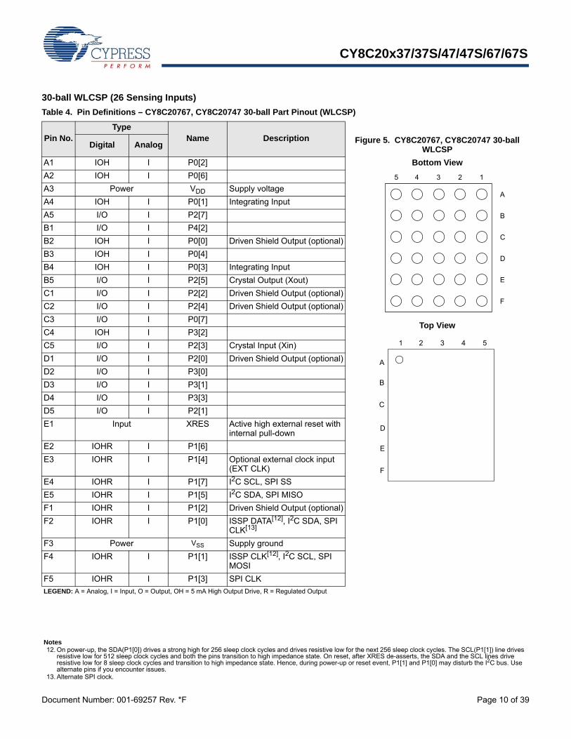
30-ball WLCSP (26 Sensing Inputs)
Table 4. Pin Definitions – CY8C20767, CY8C20747 30-ball Part Pinout (WLCSP)
Pin No.Type
Name DescriptionDigital Analog
Figure 5. CY8C20767, CY8C20747 30-ball WLCSP
A1 IOH I P0[2] Bottom View
Top View
A2 IOH I P0[6]
A3 Power VDD Supply voltage
A4 IOH I P0[1] Integrating Input
A5 I/O I P2[7]
B1 I/O I P4[2]
B2 IOH I P0[0] Driven Shield Output (optional)
B3 IOH I P0[4]
B4 IOH I P0[3] Integrating Input
B5 I/O I P2[5] Crystal Output (Xout)
C1 I/O I P2[2] Driven Shield Output (optional)
C2 I/O I P2[4] Driven Shield Output (optional)
C3 I/O I P0[7]
C4 IOH I P3[2]
C5 I/O I P2[3] Crystal Input (Xin)
D1 I/O I P2[0] Driven Shield Output (optional)
D2 I/O I P3[0]
D3 I/O I P3[1]
D4 I/O I P3[3]
D5 I/O I P2[1]
E1 Input XRES Active high external reset with internal pull-down
E2 IOHR I P1[6]
E3 IOHR I P1[4] Optional external clock input (EXT CLK)
E4 IOHR I P1[7] I2C SCL, SPI SS
E5 IOHR I P1[5] I2C SDA, SPI MISO
F1 IOHR I P1[2] Driven Shield Output (optional)
F2 IOHR I P1[0] ISSP DATA[12], I2C SDA, SPI CLK[13]
F3 Power VSS Supply ground
F4 IOHR I P1[1] ISSP CLK[12], I2C SCL, SPI MOSI
F5 IOHR I P1[3] SPI CLK
LEGEND: A = Analog, I = Input, O = Output, OH = 5 mA High Output Drive, R = Regulated Output
5 4 3 2 1
A
B
C
D
E
F
1 2 3 4 5
B
C
D
E
F
A
Notes12. On power-up, the SDA(P1[0]) drives a strong high for 256 sleep clock cycles and drives resistive low for the next 256 sleep clock cycles. The SCL(P1[1]) line drives
resistive low for 512 sleep clock cycles and both the pins transition to high impedance state. On reset, after XRES de-asserts, the SDA and the SCL lines drive resistive low for 8 sleep clock cycles and transition to high impedance state. Hence, during power-up or reset event, P1[1] and P1[0] may disturb the I2C bus. Use alternate pins if you encounter issues.
13. Alternate SPI clock.
CY8C20x37/37S/47/47S/67/67S
Document Number: 001-69257 Rev. *F Page 11 of 39
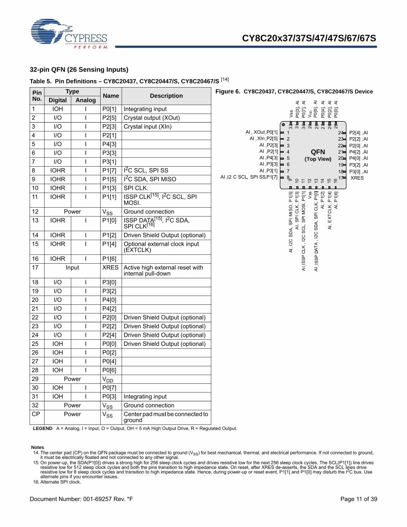
32-pin QFN (26 Sensing Inputs)
Table 5. Pin Definitions – CY8C20437, CY8C20447/S, CY8C20467/S [14]
Pin No.
TypeName Description
Figure 6. CY8C20437, CY8C20447/S, CY8C20467/S Device
Digital Analog
1 IOH I P0[1] Integrating input
2 I/O I P2[5] Crystal output (XOut)
3 I/O I P2[3] Crystal input (XIn)
4 I/O I P2[1]
5 I/O I P4[3]
6 I/O I P3[3]
7 I/O I P3[1]
8 IOHR I P1[7] I2C SCL, SPI SS
9 IOHR I P1[5] I2C SDA, SPI MISO
10 IOHR I P1[3] SPI CLK.
11 IOHR I P1[1] ISSP CLK[15], I2C SCL, SPI MOSI.
12 Power VSS Ground connection
13 IOHR I P1[0] ISSP DATA[15], I2C SDA, SPI CLK[16]
14 IOHR I P1[2] Driven Shield Output (optional)
15 IOHR I P1[4] Optional external clock input (EXTCLK)
16 IOHR I P1[6]
17 Input XRES Active high external reset with internal pull-down
18 I/O I P3[0]
19 I/O I P3[2]
20 I/O I P4[0]
21 I/O I P4[2]
22 I/O I P2[0] Driven Shield Output (optional)
23 I/O I P2[2] Driven Shield Output (optional)
24 I/O I P2[4] Driven Shield Output (optional)
25 IOH I P0[0] Driven Shield Output (optional)
26 IOH I P0[2]
27 IOH I P0[4]
28 IOH I P0[6]
29 Power VDD
30 IOH I P0[7]
31 IOH I P0[3] Integrating input
32 Power VSS Ground connection
CP Power VSS Center pad must be connected to ground
LEGEND A = Analog, I = Input, O = Output, OH = 5 mA High Output Drive, R = Regulated Output.
AI
, P0[1]
AI
, P2[5]AI , XOut
, P2[3]
AI , XIn
, P2[1]AI , P4[3]AI , P3[3]
QFN(Top View)
9 10 11 12 13 14 15 16
12
345678
2423
222120
19
1817
32
31
30
29
28
27
26
25
Vs
s
P0
[3],
AI
P0
[6],
AI
VD
D
P0
[4],
AI
P0
[2],
AI
P0
[0],
AI
AI , P3[1]AI , I2 C SCL, SPI SS, P1[7]
P2[4] , AIP2[2] , AI
P3[0] , AIXRES
AI,
I2C
SD
A,
SP
IM
ISO
,P
1[5]
AI,
SP
IC
LK
,P
1[3]
Vss
AI,
P1[
2]
AI,
EX
TC
LK
,P
1[4]
AI,
P1[
6]
P2[0] , AIP4[2] , AIP4[0] , AI
P3[2] , AI
P0
[7],
AI
AI ,
IS
SP
CL
K,
I2C
SC
L, S
PI
MO
SI,
P1[
1]
AI ,
IS
SP
DA
TA
, I2
C S
DA
, S
PI
CL
K,
P1[
0]
Notes14. The center pad (CP) on the QFN package must be connected to ground (VSS) for best mechanical, thermal, and electrical performance. If not connected to ground,
it must be electrically floated and not connected to any other signal.15. On power-up, the SDA(P1[0]) drives a strong high for 256 sleep clock cycles and drives resistive low for the next 256 sleep clock cycles. The SCL(P1[1]) line drives
resistive low for 512 sleep clock cycles and both the pins transition to high impedance state. On reset, after XRES de-asserts, the SDA and the SCL lines drive resistive low for 8 sleep clock cycles and transition to high impedance state. Hence, during power-up or reset event, P1[1] and P1[0] may disturb the I2C bus. Use alternate pins if you encounter issues.
16. Alternate SPI clock.
CY8C20x37/37S/47/47S/67/67S
Document Number: 001-69257 Rev. *F Page 12 of 39
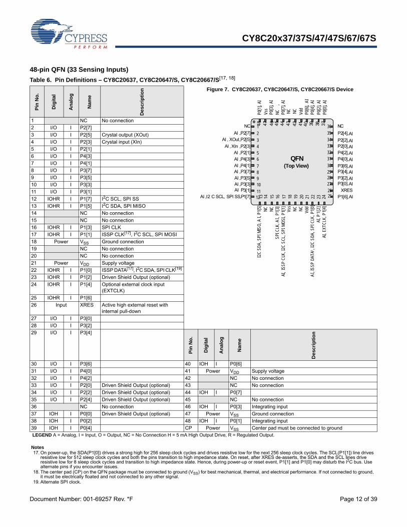
48-pin QFN (33 Sensing Inputs)
Table 6. Pin Definitions – CY8C20637, CY8C20647/S, CY8C20667/S[17, 18]
Pin
No
.
Dig
ita
l
An
alo
g
Nam
e
De
scri
pti
on Figure 7. CY8C20637, CY8C20647/S, CY8C20667/S Device
1 NC No connection
2 I/O I P2[7]
3 I/O I P2[5] Crystal output (XOut)
4 I/O I P2[3] Crystal input (XIn)
5 I/O I P2[1]
6 I/O I P4[3]
7 I/O I P4[1]
8 I/O I P3[7]
9 I/O I P3[5]
10 I/O I P3[3]
11 I/O I P3[1]
12 IOHR I P1[7] I2C SCL, SPI SS
13 IOHR I P1[5] I2C SDA, SPI MISO
14 NC No connection
15 NC No connection
16 IOHR I P1[3] SPI CLK
17 IOHR I P1[1] ISSP CLK[17], I2C SCL, SPI MOSI
18 Power VSS Ground connection
19 NC No connection
20 NC No connection
21 Power VDD Supply voltage
22 IOHR I P1[0] ISSP DATA[17], I2C SDA, SPI CLK[19]
23 IOHR I P1[2] Driven Shield Output (optional)
24 IOHR I P1[4] Optional external clock input (EXTCLK)
25 IOHR I P1[6]
26 Input XRES Active high external reset with internal pull-down
27 I/O I P3[0]
28 I/O I P3[2]
29 I/O I P3[4]
Pin
No
.
Dig
ital
An
alo
g
Nam
e
Des
cri
pti
on
30 I/O I P3[6] 40 IOH I P0[6]
31 I/O I P4[0] 41 Power VDD Supply voltage
32 I/O I P4[2] 42 NC No connection
33 I/O I P2[0] Driven Shield Output (optional) 43 NC No connection
34 I/O I P2[2] Driven Shield Output (optional) 44 IOH I P0[7]
35 I/O I P2[4] Driven Shield Output (optional) 45 NC No connection
36 NC No connection 46 IOH I P0[3] Integrating input
37 IOH I P0[0] Driven Shield Output (optional) 47 Power VSS Ground connection
38 IOH I P0[2] 48 IOH I P0[1] Integrating input
39 IOH I P0[4] CP Power VSS Center pad must be connected to ground LEGEND A = Analog, I = Input, O = Output, NC = No Connection H = 5 mA High Output Drive, R = Regulated Output.
QFN(Top View)
Vss
P0[3
],AI
NC
,P0
[7],
AI
Vdd
P0[6
],A
I
P0[2
],AI
P0[0
],AI
10
1112
AI , P2[7]
NC
AI , XOut, P2[5]
AI , XIn , P2[3]AI , P2[1]
AI , P4[3]AI , P4[1]AI , P3[7]AI , P3[5]AI , P3[3]AI P3[1]
AI , I2 C SCL, SPI SS, P1[7]
35
34333231
30292827
2625
3648 47 4 6 45 44 43 42 41 4 0 39 38 37
P2[4], AI
P2[2], AIP2[0], AIP4[2], AIP4[0], AIP3[6], AIP3[4], AIP3[2], AIP3[0], AI
XRESP1[6], AI
NC1
2
3456
789
13 14 15 16 17 18 19 20 21 22 23 24
I2C
SDA,
SPIM
ISO
,AI,
P1[5
]NC
SPIC
LK,A
I,P1
[3]
AI,
ISSP
CLK
,I2C
SCL,
SPIM
OSI
,P1[
1] Vss
NC NC
Vdd
AI,
ISSP
DAT
A1,I
2CSD
A,SP
ICLK
,P1[
0]AI
,P1[
2]AI
,EXT
CLK
,P1[
4]NC
NC
NC
P0[4
],AI
P0[1
],AI
Notes17. On power-up, the SDA(P1[0]) drives a strong high for 256 sleep clock cycles and drives resistive low for the next 256 sleep clock cycles. The SCL(P1[1]) line drives
resistive low for 512 sleep clock cycles and both the pins transition to high impedance state. On reset, after XRES de-asserts, the SDA and the SCL lines drive resistive low for 8 sleep clock cycles and transition to high impedance state. Hence, during power-up or reset event, P1[1] and P1[0] may disturb the I2C bus. Use alternate pins if you encounter issues.
18. The center pad (CP) on the QFN package must be connected to ground (VSS) for best mechanical, thermal, and electrical performance. If not connected to ground, it must be electrically floated and not connected to any other signal.
19. Alternate SPI clock.
CY8C20x37/37S/47/47S/67/67S
Document Number: 001-69257 Rev. *F Page 13 of 39
Electrical Specifications
This section presents the DC and AC electrical specifications of the CY8C20x37/47/67/S PSoC devices. For the latest electricalspecifications, confirm that you have the most recent datasheet by visiting the web at http://www.cypress.com/psoc.
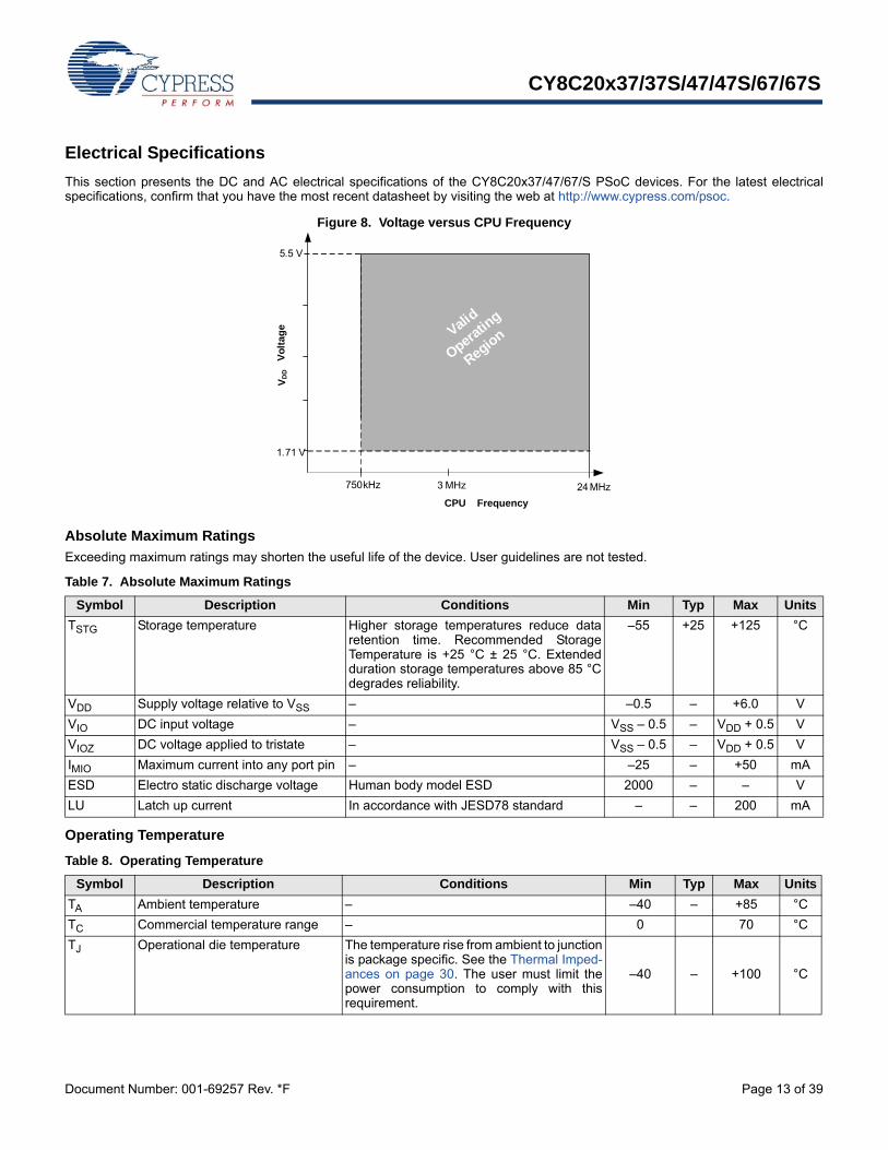
Figure 8. Voltage versus CPU Frequency
Absolute Maximum Ratings
Exceeding maximum ratings may shorten the useful life of the device. User guidelines are not tested.
Operating Temperature
5.5 V
750 kHz 24 MHz
CPU Frequency
VD
D V
olt
age
1.71 V
3 MHz
Valid
Operatin
g
Region
Table 7. Absolute Maximum Ratings
Symbol Description Conditions Min Typ Max Units
TSTG Storage temperature Higher storage temperatures reduce dataretention time. Recommended StorageTemperature is +25 °C ± 25 °C. Extendedduration storage temperatures above 85 °Cdegrades reliability.
–55 +25 +125 °C
VDD Supply voltage relative to VSS – –0.5 – +6.0 V
VIO DC input voltage – VSS – 0.5 – VDD + 0.5 V
VIOZ DC voltage applied to tristate – VSS – 0.5 – VDD + 0.5 V
IMIO Maximum current into any port pin – –25 – +50 mA
ESD Electro static discharge voltage Human body model ESD 2000 – – V
LU Latch up current In accordance with JESD78 standard – – 200 mA
Table 8. Operating Temperature
Symbol Description Conditions Min Typ Max Units
TA Ambient temperature – –40 – +85 °C
TC Commercial temperature range – 0 70 °C
TJ Operational die temperature The temperature rise from ambient to junctionis package specific. See the Thermal Imped-ances on page 30. The user must limit thepower consumption to comply with thisrequirement.
–40 – +100 °C
CY8C20x37/37S/47/47S/67/67S
Document Number: 001-69257 Rev. *F Page 14 of 39
DC Chip-Level Specifications
The following table lists guaranteed maximum and minimum specifications for the entire voltage and temperature ranges.
Table 9. DC Chip-Level Specifications
Symbol Description Conditions Min Typ Max Units
VDD[20, 21, 22] Supply voltage See table DC POR and LVD Specifications on
page 191.71 – 5.50 V
IDD24 Supply current, IMO = 24 MHz Conditions are VDD 3.0 V, TA = 25 °C, CPU = 24 MHz. CapSense running at 12 MHz, no I/O sourcing current
– 2.88 4.00 mA
IDD12 Supply current, IMO = 12 MHz Conditions are VDD 3.0 V, TA = 25 °C, CPU = 12 MHz. CapSense running at 12 MHz, no I/O sourcing current
– 1.71 2.60 mA
IDD6 Supply current, IMO = 6 MHz Conditions are VDD 3.0 V, TA = 25 °C, CPU = 6 MHz. CapSense running at 6 MHz, no I/O sourcing current
– 1.16 1.80 mA
ISB0 Deep sleep current VDD 3.0 V, TA = 25 °C, I/O regulator turned off – 0.10 1.1 A
ISB1 Standby current with POR, LVD and sleep timer
VDD 3.0 V, TA = 25 °C, I/O regulator turned off – 1.07 1.50 A
ISBI2C Standby current with I2C enabled
Conditions are VDD = 3.3 V, TA = 25 °C and CPU = 24 MHz
– 1.64 – A
Notes20. When VDD remains in the range from 1.71 V to 1.9 V for more than 50 µs, the slew rate when moving from the 1.71 V to 1.9 V range to greater than 2 V must be
slower than 1 V/500 µs to avoid triggering POR. The only other restriction on slew rates for any other voltage range or transition is the SRPOWER_UP parameter.21. If powering down in standby sleep mode, to properly detect and recover from a VDD brown out condition any of the following actions must be taken:
a. Bring the device out of sleep before powering down.b. Assure that VDD falls below 100 mV before powering back up.c. Set the No Buzz bit in the OSC_CR0 register to keep the voltage monitoring circuit powered during sleep.d. Increase the buzz rate to assure that the falling edge of VDD is captured. The rate is configured through the PSSDC bits in the SLP_CFG register. For the referenced registers, refer to the Technical Reference Manual. In deep sleep/standby sleep mode, additional low power voltage monitoring circuitry allows VDD brown out conditions to be detected and resets the device when VDD goes lower than 1.1 V at edge rates slower than 1 V/ms.
22. For proper CapSense block functionality, if the drop in VDD exceeds 5% of the base VDD, the rate at which VDD drops should not exceed 200 mV/s. Base VDD can be between 1.8 V and 5.5 V.
CY8C20x37/37S/47/47S/67/67S
Document Number: 001-69257 Rev. *F Page 15 of 39
DC GPIO Specifications
The following tables list guaranteed maximum and minimum specifications for the voltage and temperature ranges: 3.0 V to 5.5 V and–40 °C TA 85 °C, 2.4 V to 3.0 V and –40 °C TA 85 °C, or 1.71 V to 2.4 V and –40 °C TA 85 °C, respectively. Typicalparameters apply to 5 V and 3.3 V at 25 °C and are for design guidance only.
Table 10. 3.0 V to 5.5 V DC GPIO Specifications
Symbol Description Conditions Min Typ Max Units
RPU Pull-up resistor – 4 5.60 8 k
VOH1 High output voltagePort 2 or 3 pins
IOH < 10 A, maximum of 10 mA source current in all I/Os
VDD – 0.20 – – V
VOH2 High output voltagePort 2 or 3 Pins
IOH = 1 mA, maximum of 20 mA source current in all I/Os
VDD – 0.90 – – V
VOH3 High output voltagePort 0 or 1 pins with LDO regulator Disabled for port 1
IOH < 10 A, maximum of 10 mA source current in all I/Os
VDD – 0.20 – – V
VOH4 High output voltagePort 0 or 1 pins with LDO regulator Disabled for port 1
IOH = 5 mA, maximum of 20 mA source current in all I/Os
VDD – 0.90 – – V
VOH5 High output voltagePort 1 Pins with LDO Regulator Enabled for 3 V out
IOH < 10 A, VDD > 3.1 V, maximum of 4 I/Os all sourcing 5 mA
2.85 3.00 3.30 V
VOH6 High output voltagePort 1 pins with LDO regulator enabled for 3 V out
IOH = 5 mA, VDD > 3.1 V, maximum of 20 mA source current in all I/Os
2.20 – – V
VOH7 High output voltagePort 1 pins with LDO enabled for 2.5 V out
IOH < 10 A, VDD > 2.7 V, maximum of 20 mA source current in all I/Os
2.35 2.50 2.75 V
VOH8 High output voltagePort 1 pins with LDO enabled for 2.5 V out
IOH = 2 mA, VDD > 2.7 V, maximum of 20 mA source current in all I/Os
1.90 – – V
VOH9 High output voltagePort 1 pins with LDO enabled for 1.8 V out
IOH < 10 A, VDD > 2.7 V, maximum of 20 mA source current in all I/Os
1.60 1.80 2.10 V
VOH10 High output voltagePort 1 pins with LDO enabled for 1.8 V out
IOH = 1 mA, VDD > 2.7 V, maximum of 20 mA source current in all I/Os
1.20 – – V
VOL Low output voltage IOL = 25 mA, VDD > 3.3 V, maximum of 60 mA sink current on even port pins (for example, P0[2] and P1[4]) and 60 mA sink current on odd port pins (for example, P0[3] and P1[5])
– – 0.75 V
VIL Input low voltage – – – 0.80 V
VIH Input high voltage – 2.00 – – V
VH Input hysteresis voltage – – 80 – mV
IIL Input leakage (Absolute Value) – – 0.001
1 A
CPIN Pin capacitance Package and pin dependent Temp = 25 °C
0.50 1.70 7 pF
VILLVT3.3 Input Low Voltage with low threshold enable set, Enable for Port1
Bit3 of IO_CFG1 set to enable low threshold voltage of Port1 input
0.8 V – –
VIHLVT3.3 Input High Voltage with low threshold enable set, Enable for Port1
Bit3 of IO_CFG1 set to enable low threshold voltage of Port1 input
1.4 – – V
VILLVT5.5 Input Low Voltage with low threshold enable set, Enable for Port1
Bit3 of IO_CFG1 set to enable low threshold voltage of Port1 input
0.8 V – –
VIHLVT5.5 Input High Voltage with low threshold enable set, Enable for Port1
Bit3 of IO_CFG1 set to enable low threshold voltage of Port1 input
1.7 – – V
CY8C20x37/37S/47/47S/67/67S
Document Number: 001-69257 Rev. *F Page 16 of 39
Table 11. 2.4 V to 3.0 V DC GPIO Specifications
Symbol Description Conditions Min Typ Max Units
RPU Pull-up resistor – 4 5.60 8 k
VOH1 High output voltagePort 2 or 3 pins
IOH < 10 A, maximum of 10 mA source current in all I/Os
VDD - 0.20 – – V
VOH2 High output voltagePort 2 or 3 Pins
IOH = 0.2 mA, maximum of 10 mA source current in all I/Os
VDD - 0.40 – – V
VOH3 High output voltagePort 0 or 1 pins with LDO regulator Disabled for port 1
IOH < 10 A, maximum of 10 mA source current in all I/Os
VDD - 0.20 – – V
VOH4 High output voltagePort 0 or 1 pins with LDO regulator Disabled for Port 1
IOH = 2 mA, maximum of 10 mA source current in all I/Os
VDD - 0.50 – – V
VOH5A High output voltagePort 1 pins with LDO enabled for 1.8 V out
IOH < 10 A, VDD > 2.4 V, maximum of 20 mA source current in all I/Os
1.50 1.80 2.10 V
VOH6A High output voltagePort 1 pins with LDO enabled for 1.8 V out
IOH = 1 mA, VDD > 2.4 V, maximum of 20 mA source current in all I/Os
1.20 – – V
VOL Low output voltage IOL = 10 mA, maximum of 30 mA sinkcurrent on even port pins (for example,P0[2] and P1[4]) and 30 mA sinkcurrent on odd port pins (for example,P0[3] and P1[5])
– – 0.75 V
VIL Input low voltage – – – 0.72 V
VIH Input high voltage – 1.40 – V
VH Input hysteresis voltage – – 80 – mV
IIL Input leakage (absolute value) – – 1 1000 nA
CPIN Capacitive load on pins Package and pin dependentTemp = 25 C
0.50 1.70 7 pF
VILLVT2.5 Input Low Voltage with low threshold enable set, Enable for Port1
Bit3 of IO_CFG1 set to enable lowthreshold voltage of Port1 input
0.7 V –
VIHLVT2.5 Input High Voltage with low threshold enable set, Enable for Port1
Bit3 of IO_CFG1 set to enable lowthreshold voltage of Port1 input
1.2 – V
Table 12. 1.71 V to 2.4 V DC GPIO Specifications
Symbol Description Conditions Min Typ Max Units
RPU Pull-up resistor – 4 5.60 8 k
VOH1 High output voltagePort 2 or 3 pins
IOH = 10 A, maximum of 10 mAsource current in all I/Os
VDD – 0.20 – – V
VOH2 High output voltagePort 2 or 3 pins
IOH = 0.5 mA, maximum of 10 mAsource current in all I/Os
VDD – 0.50 – – V
VOH3 High output voltagePort 0 or 1 pins with LDO regulator Disabled for Port 1
IOH = 100 A, maximum of 10 mAsource current in all I/Os
VDD – 0.20 – – V
VOH4 High output voltagePort 0 or 1 Pins with LDO Regulator Disabled for Port 1
IOH = 2 mA, maximum of 10 mA sourcecurrent in all I/Os
VDD – 0.50 – – V
CY8C20x37/37S/47/47S/67/67S
Document Number: 001-69257 Rev. *F Page 17 of 39
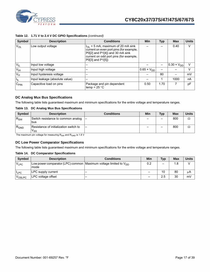
DC Analog Mux Bus Specifications
The following table lists guaranteed maximum and minimum specifications for the entire voltage and temperature ranges.
DC Low Power Comparator Specifications
The following table lists guaranteed maximum and minimum specifications for the entire voltage and temperature ranges.
VOL Low output voltage IOL = 5 mA, maximum of 20 mA sink current on even port pins (for example, P0[2] and P1[4]) and 30 mA sink current on odd port pins (for example, P0[3] and P1[5])
– – 0.40 V
VIL Input low voltage – – – 0.30 × VDD V
VIH Input high voltage – 0.65 × VDD – – V
VH Input hysteresis voltage – – 80 – mV
IIL Input leakage (absolute value) – – 1 1000 nA
CPIN Capacitive load on pins Package and pin dependent temp = 25 C
0.50 1.70 7 pF
Table 12. 1.71 V to 2.4 V DC GPIO Specifications (continued)
Symbol Description Conditions Min Typ Max Units
Table 13. DC Analog Mux Bus Specifications
Symbol Description Conditions Min Typ Max Units
RSW Switch resistance to common analog bus
– – – 800
RGND Resistance of initialization switch to VSS
– – – 800
The maximum pin voltage for measuring RSW and RGND is 1.8 V
Table 14. DC Comparator Specifications
Symbol Description Conditions Min Typ Max Units
VLPC Low power comparator (LPC) common mode
Maximum voltage limited to VDD 0.2 – 1.8 V
ILPC LPC supply current – – 10 80 A
VOSLPC LPC voltage offset – – 2.5 30 mV
CY8C20x37/37S/47/47S/67/67S
Document Number: 001-69257 Rev. *F Page 18 of 39
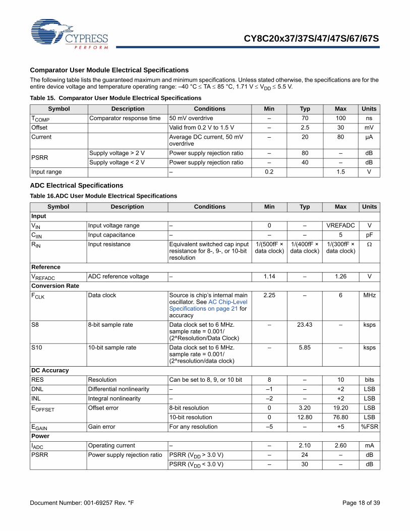
Comparator User Module Electrical Specifications
The following table lists the guaranteed maximum and minimum specifications. Unless stated otherwise, the specifications are for the entire device voltage and temperature operating range: –40 °C TA 85 °C, 1.71 V VDD 5.5 V.
ADC Electrical Specifications
Table 15. Comparator User Module Electrical Specifications
Symbol Description Conditions Min Typ Max Units
TCOMP Comparator response time 50 mV overdrive – 70 100 ns
Offset Valid from 0.2 V to 1.5 V – 2.5 30 mV
Current Average DC current, 50 mV overdrive
– 20 80 µA
PSRRSupply voltage > 2 V Power supply rejection ratio – 80 – dB
Supply voltage < 2 V Power supply rejection ratio – 40 – dB
Input range – 0.2 1.5 V
Table 16.ADC User Module Electrical Specifications
Symbol Description Conditions Min Typ Max Units
Input
VIN Input voltage range – 0 – VREFADC V
CIIN Input capacitance – – – 5 pF
RIN Input resistance Equivalent switched cap input resistance for 8-, 9-, or 10-bit resolution
1/(500fF × data clock)
1/(400fF × data clock)
1/(300fF × data clock)
Reference
VREFADC ADC reference voltage – 1.14 – 1.26 V
Conversion Rate
FCLK Data clock Source is chip’s internal main oscillator. See AC Chip-Level Specifications on page 21 for accuracy
2.25 – 6 MHz
S8 8-bit sample rate Data clock set to 6 MHz. sample rate = 0.001/ (2^Resolution/Data Clock)
– 23.43 – ksps
S10 10-bit sample rate Data clock set to 6 MHz. sample rate = 0.001/ (2^resolution/data clock)
– 5.85 – ksps
DC Accuracy
RES Resolution Can be set to 8, 9, or 10 bit 8 – 10 bits
DNL Differential nonlinearity – –1 – +2 LSB
INL Integral nonlinearity – –2 – +2 LSB
EOFFSET Offset error 8-bit resolution 0 3.20 19.20 LSB
10-bit resolution 0 12.80 76.80 LSB
EGAIN Gain error For any resolution –5 – +5 %FSR
Power
IADC Operating current – – 2.10 2.60 mA
PSRR Power supply rejection ratio PSRR (VDD > 3.0 V) – 24 – dB
PSRR (VDD < 3.0 V) – 30 – dB
CY8C20x37/37S/47/47S/67/67S
Document Number: 001-69257 Rev. *F Page 19 of 39
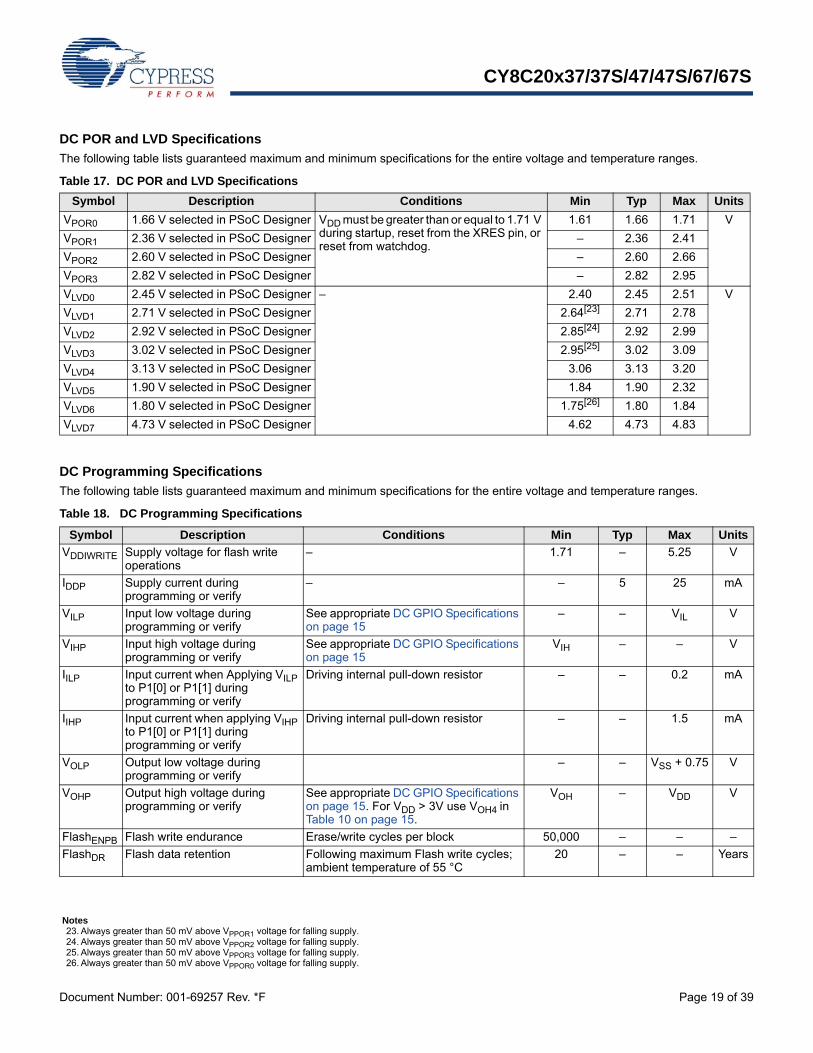
DC POR and LVD Specifications
The following table lists guaranteed maximum and minimum specifications for the entire voltage and temperature ranges.
DC Programming Specifications
The following table lists guaranteed maximum and minimum specifications for the entire voltage and temperature ranges.
Table 17. DC POR and LVD Specifications
Symbol Description Conditions Min Typ Max Units
VPOR0 1.66 V selected in PSoC Designer VDD must be greater than or equal to 1.71 V during startup, reset from the XRES pin, or reset from watchdog.
1.61 1.66 1.71 V
VPOR1 2.36 V selected in PSoC Designer – 2.36 2.41
VPOR2 2.60 V selected in PSoC Designer – 2.60 2.66
VPOR3 2.82 V selected in PSoC Designer – 2.82 2.95
VLVD0 2.45 V selected in PSoC Designer – 2.40 2.45 2.51 V
VLVD1 2.71 V selected in PSoC Designer 2.64[23] 2.71 2.78
VLVD2 2.92 V selected in PSoC Designer 2.85[24] 2.92 2.99
VLVD3 3.02 V selected in PSoC Designer 2.95[25] 3.02 3.09
VLVD4 3.13 V selected in PSoC Designer 3.06 3.13 3.20
VLVD5 1.90 V selected in PSoC Designer 1.84 1.90 2.32
VLVD6 1.80 V selected in PSoC Designer 1.75[26] 1.80 1.84
VLVD7 4.73 V selected in PSoC Designer 4.62 4.73 4.83
Table 18. DC Programming Specifications
Symbol Description Conditions Min Typ Max Units
VDDIWRITE Supply voltage for flash write operations
– 1.71 – 5.25 V
IDDP Supply current during programming or verify
– – 5 25 mA
VILP Input low voltage during programming or verify
See appropriate DC GPIO Specifications on page 15
– – VIL V
VIHP Input high voltage during programming or verify
See appropriate DC GPIO Specifications on page 15
VIH – – V
IILP Input current when Applying VILP to P1[0] or P1[1] during programming or verify
Driving internal pull-down resistor – – 0.2 mA
IIHP Input current when applying VIHP to P1[0] or P1[1] during programming or verify
Driving internal pull-down resistor – – 1.5 mA
VOLP Output low voltage during programming or verify
– – VSS + 0.75 V
VOHP Output high voltage during programming or verify
See appropriate DC GPIO Specifications on page 15. For VDD > 3V use VOH4 in Table 10 on page 15.
VOH – VDD V
FlashENPB Flash write endurance Erase/write cycles per block 50,000 – – –
FlashDR Flash data retention Following maximum Flash write cycles; ambient temperature of 55 °C
20 – – Years
Notes23. Always greater than 50 mV above VPPOR1 voltage for falling supply.24. Always greater than 50 mV above VPPOR2 voltage for falling supply.25. Always greater than 50 mV above VPPOR3 voltage for falling supply.26. Always greater than 50 mV above VPPOR0 voltage for falling supply.
CY8C20x37/37S/47/47S/67/67S
Document Number: 001-69257 Rev. *F Page 20 of 39
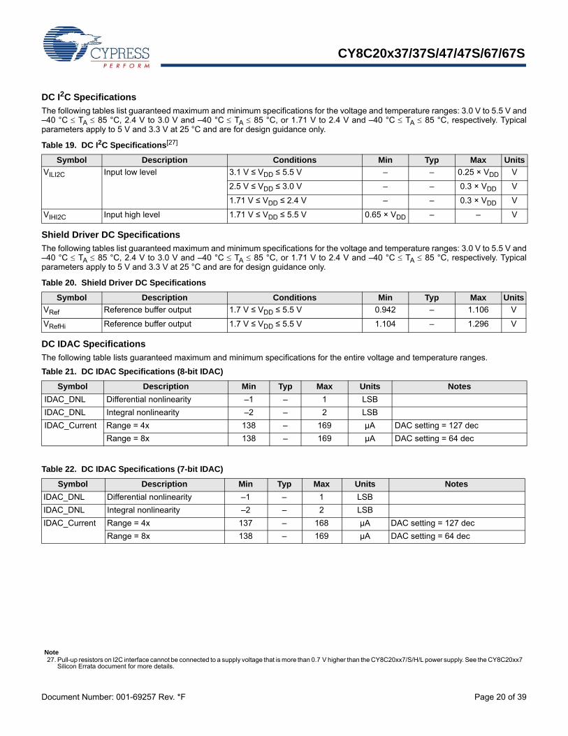
DC I2C Specifications
The following tables list guaranteed maximum and minimum specifications for the voltage and temperature ranges: 3.0 V to 5.5 V and–40 °C TA 85 °C, 2.4 V to 3.0 V and –40 °C TA 85 °C, or 1.71 V to 2.4 V and –40 °C TA 85 °C, respectively. Typicalparameters apply to 5 V and 3.3 V at 25 °C and are for design guidance only.
Shield Driver DC Specifications
The following tables list guaranteed maximum and minimum specifications for the voltage and temperature ranges: 3.0 V to 5.5 V and–40 °C TA 85 °C, 2.4 V to 3.0 V and –40 °C TA 85 °C, or 1.71 V to 2.4 V and –40 °C TA 85 °C, respectively. Typicalparameters apply to 5 V and 3.3 V at 25 °C and are for design guidance only.
DC IDAC Specifications
The following table lists guaranteed maximum and minimum specifications for the entire voltage and temperature ranges.
Table 19. DC I2C Specifications[27]
Symbol Description Conditions Min Typ Max Units
VILI2C Input low level 3.1 V ≤ VDD ≤ 5.5 V – – 0.25 × VDD V
2.5 V ≤ VDD ≤ 3.0 V – – 0.3 × VDD V
1.71 V ≤ VDD ≤ 2.4 V – – 0.3 × VDD V
VIHI2C Input high level 1.71 V ≤ VDD ≤ 5.5 V 0.65 × VDD – – V
Table 20. Shield Driver DC Specifications
Symbol Description Conditions Min Typ Max Units
VRef Reference buffer output 1.7 V ≤ VDD ≤ 5.5 V 0.942 – 1.106 V
VRefHi Reference buffer output 1.7 V ≤ VDD ≤ 5.5 V 1.104 – 1.296 V
Table 21. DC IDAC Specifications (8-bit IDAC)
Symbol Description Min Typ Max Units Notes
IDAC_DNL Differential nonlinearity –1 – 1 LSB
IDAC_DNL Integral nonlinearity –2 – 2 LSB
IDAC_Current Range = 4x 138 – 169 µA DAC setting = 127 dec
Range = 8x 138 – 169 µA DAC setting = 64 dec
Table 22. DC IDAC Specifications (7-bit IDAC)
Symbol Description Min Typ Max Units Notes
IDAC_DNL Differential nonlinearity –1 – 1 LSB
IDAC_DNL Integral nonlinearity –2 – 2 LSB
IDAC_Current Range = 4x 137 – 168 µA DAC setting = 127 dec
Range = 8x 138 – 169 µA DAC setting = 64 dec
Note27. Pull-up resistors on I2C interface cannot be connected to a supply voltage that is more than 0.7 V higher than the CY8C20xx7/S/H/L power supply. See the CY8C20xx7
Silicon Errata document for more details.
CY8C20x37/37S/47/47S/67/67S
Document Number: 001-69257 Rev. *F Page 21 of 39
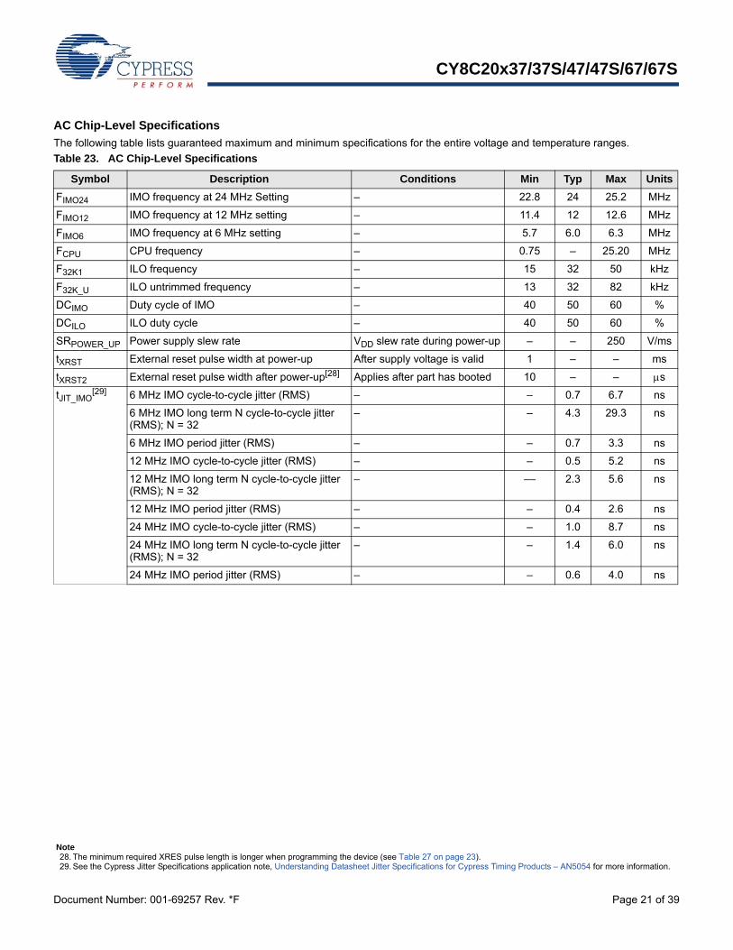
AC Chip-Level Specifications
The following table lists guaranteed maximum and minimum specifications for the entire voltage and temperature ranges.
Table 23. AC Chip-Level Specifications
Symbol Description Conditions Min Typ Max Units
FIMO24 IMO frequency at 24 MHz Setting – 22.8 24 25.2 MHz
FIMO12 IMO frequency at 12 MHz setting – 11.4 12 12.6 MHz
FIMO6 IMO frequency at 6 MHz setting – 5.7 6.0 6.3 MHz
FCPU CPU frequency – 0.75 – 25.20 MHz
F32K1 ILO frequency – 15 32 50 kHz
F32K_U ILO untrimmed frequency – 13 32 82 kHz
DCIMO Duty cycle of IMO – 40 50 60 %
DCILO ILO duty cycle – 40 50 60 %
SRPOWER_UP Power supply slew rate VDD slew rate during power-up – – 250 V/ms
tXRST External reset pulse width at power-up After supply voltage is valid 1 – – ms
tXRST2 External reset pulse width after power-up[28] Applies after part has booted 10 – – s
tJIT_IMO[29] 6 MHz IMO cycle-to-cycle jitter (RMS) – – 0.7 6.7 ns
6 MHz IMO long term N cycle-to-cycle jitter (RMS); N = 32
– – 4.3 29.3 ns
6 MHz IMO period jitter (RMS) – – 0.7 3.3 ns
12 MHz IMO cycle-to-cycle jitter (RMS) – – 0.5 5.2 ns
12 MHz IMO long term N cycle-to-cycle jitter (RMS); N = 32
– –– 2.3 5.6 ns
12 MHz IMO period jitter (RMS) – – 0.4 2.6 ns
24 MHz IMO cycle-to-cycle jitter (RMS) – – 1.0 8.7 ns
24 MHz IMO long term N cycle-to-cycle jitter (RMS); N = 32
– – 1.4 6.0 ns
24 MHz IMO period jitter (RMS) – – 0.6 4.0 ns
Note28. The minimum required XRES pulse length is longer when programming the device (see Table 27 on page 23).29. See the Cypress Jitter Specifications application note, Understanding Datasheet Jitter Specifications for Cypress Timing Products – AN5054 for more information.
CY8C20x37/37S/47/47S/67/67S
Document Number: 001-69257 Rev. *F Page 22 of 39
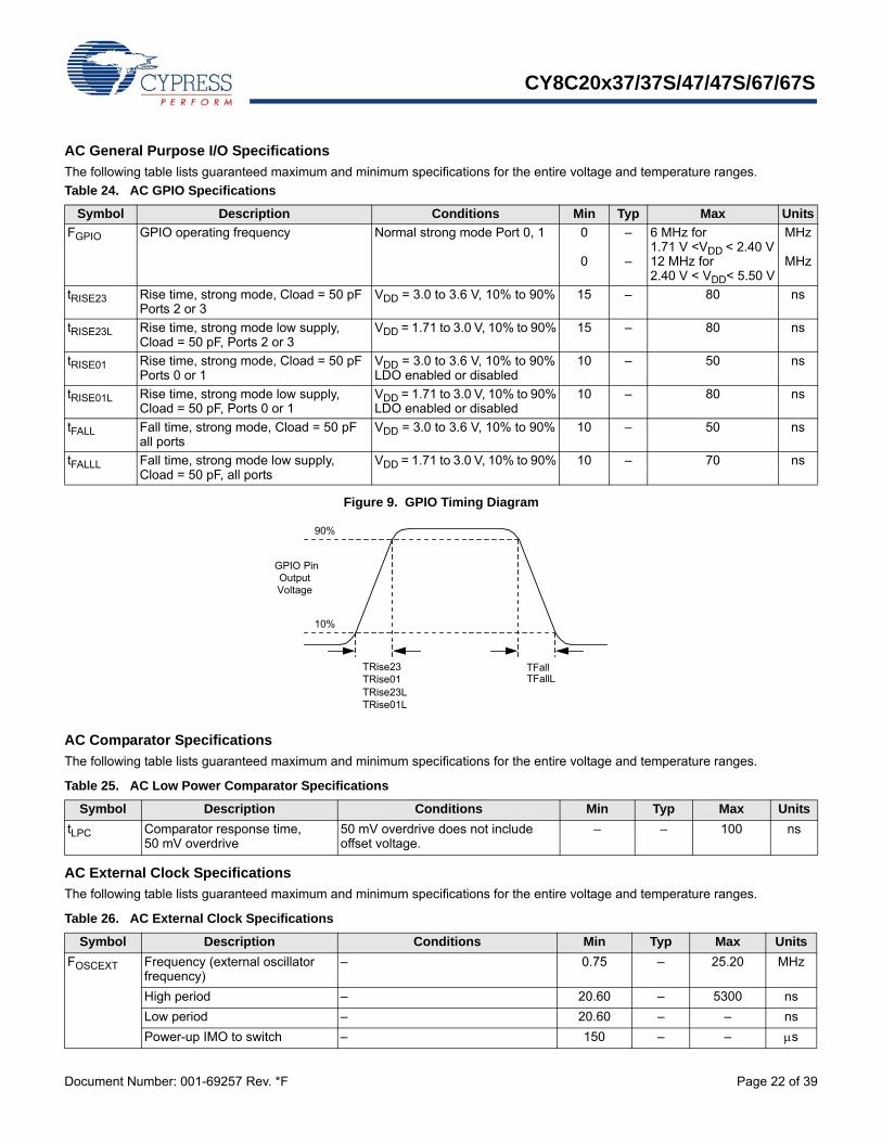
AC General Purpose I/O Specifications
The following table lists guaranteed maximum and minimum specifications for the entire voltage and temperature ranges.
Figure 9. GPIO Timing Diagram
AC Comparator Specifications
The following table lists guaranteed maximum and minimum specifications for the entire voltage and temperature ranges.
AC External Clock Specifications
The following table lists guaranteed maximum and minimum specifications for the entire voltage and temperature ranges.
Table 24. AC GPIO Specifications
Symbol Description Conditions Min Typ Max Units
FGPIO GPIO operating frequency Normal strong mode Port 0, 1 0
0
–
–
6 MHz for 1.71 V <VDD < 2.40 V12 MHz for2.40 V < VDD< 5.50 V
MHz
MHz
tRISE23 Rise time, strong mode, Cload = 50 pFPorts 2 or 3
VDD = 3.0 to 3.6 V, 10% to 90% 15 – 80 ns
tRISE23L Rise time, strong mode low supply, Cload = 50 pF, Ports 2 or 3
VDD = 1.71 to 3.0 V, 10% to 90% 15 – 80 ns
tRISE01 Rise time, strong mode, Cload = 50 pFPorts 0 or 1
VDD = 3.0 to 3.6 V, 10% to 90%LDO enabled or disabled
10 – 50 ns
tRISE01L Rise time, strong mode low supply, Cload = 50 pF, Ports 0 or 1
VDD = 1.71 to 3.0 V, 10% to 90%LDO enabled or disabled
10 – 80 ns
tFALL Fall time, strong mode, Cload = 50 pFall ports
VDD = 3.0 to 3.6 V, 10% to 90% 10 – 50 ns
tFALLL Fall time, strong mode low supply, Cload = 50 pF, all ports
VDD = 1.71 to 3.0 V, 10% to 90% 10 – 70 ns
TFallTRise23TRise01
90%
10%
GPIO PinOutputVoltage
TRise23LTRise01L
TFallL
Table 25. AC Low Power Comparator Specifications
Symbol Description Conditions Min Typ Max Units
tLPC Comparator response time, 50 mV overdrive
50 mV overdrive does not include offset voltage.
– – 100 ns
Table 26. AC External Clock Specifications
Symbol Description Conditions Min Typ Max Units
FOSCEXT Frequency (external oscillator frequency)
– 0.75 – 25.20 MHz
High period – 20.60 – 5300 ns
Low period – 20.60 – – ns
Power-up IMO to switch – 150 – – s
CY8C20x37/37S/47/47S/67/67S
Document Number: 001-69257 Rev. *F Page 23 of 39
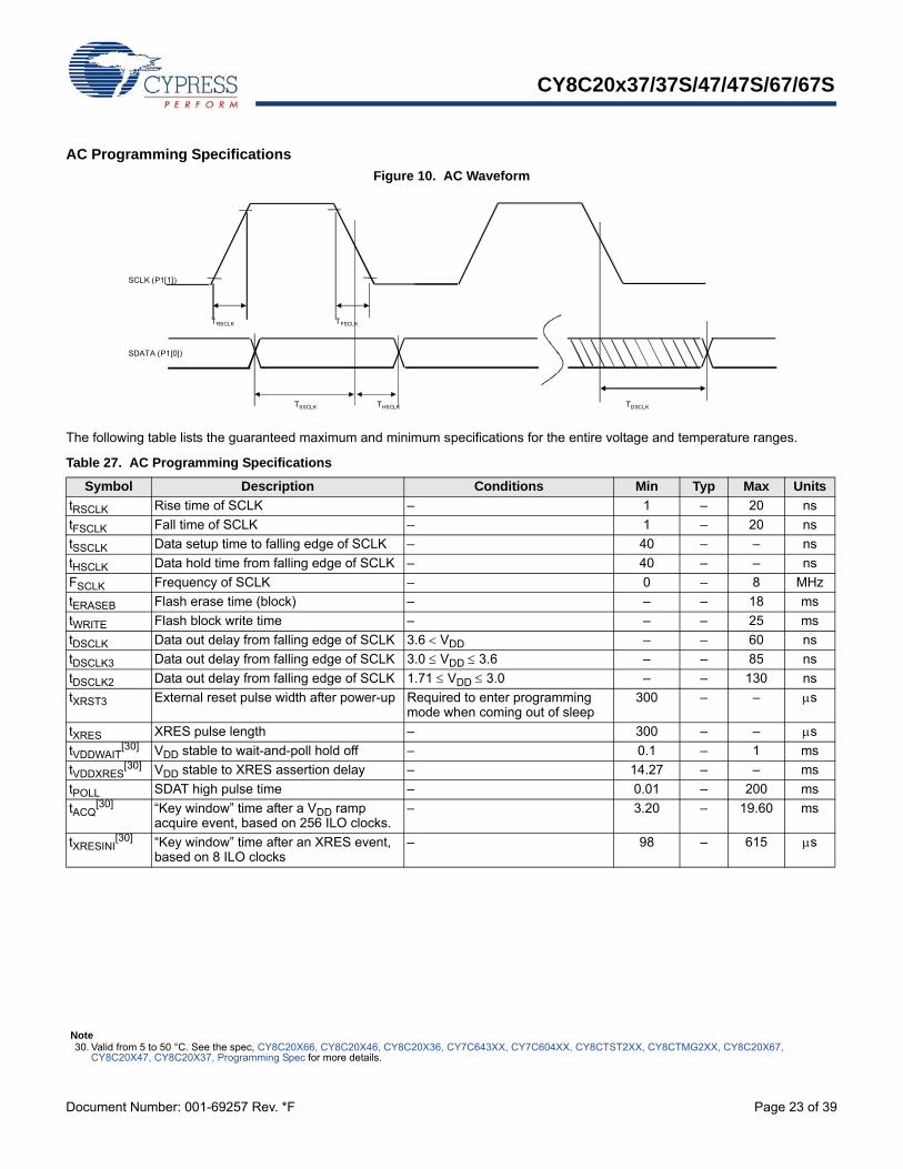
AC Programming Specifications
Figure 10. AC Waveform
The following table lists the guaranteed maximum and minimum specifications for the entire voltage and temperature ranges.
Table 27. AC Programming Specifications
Symbol Description Conditions Min Typ Max Units
tRSCLK Rise time of SCLK – 1 – 20 ns
tFSCLK Fall time of SCLK – 1 – 20 ns
tSSCLK Data setup time to falling edge of SCLK – 40 – – ns
tHSCLK Data hold time from falling edge of SCLK – 40 – – ns
FSCLK Frequency of SCLK – 0 – 8 MHz
tERASEB Flash erase time (block) – – – 18 ms
tWRITE Flash block write time – – – 25 ms
tDSCLK Data out delay from falling edge of SCLK 3.6 VDD – – 60 ns
tDSCLK3 Data out delay from falling edge of SCLK 3.0 VDD 3.6 – – 85 ns
tDSCLK2 Data out delay from falling edge of SCLK 1.71 VDD 3.0 – – 130 ns
tXRST3 External reset pulse width after power-up Required to enter programming mode when coming out of sleep
300 – – s
tXRES XRES pulse length – 300 – – s
tVDDWAIT[30] VDD stable to wait-and-poll hold off – 0.1 – 1 ms
tVDDXRES[30] VDD stable to XRES assertion delay – 14.27 – – ms
tPOLL SDAT high pulse time – 0.01 – 200 ms
tACQ[30] “Key window” time after a VDD ramp
acquire event, based on 256 ILO clocks.– 3.20 – 19.60 ms
tXRESINI[30] “Key window” time after an XRES event,
based on 8 ILO clocks– 98 – 615 s
SCLK (P1[1])
TRSCLK TFSCLK
SDATA (P1[0])
TSSCLK THSCLK TDSCLK
Note30. Valid from 5 to 50 °C. See the spec, CY8C20X66, CY8C20X46, CY8C20X36, CY7C643XX, CY7C604XX, CY8CTST2XX, CY8CTMG2XX, CY8C20X67,
CY8C20X47, CY8C20X37, Programming Spec for more details.
CY8C20x37/37S/47/47S/67/67S
Document Number: 001-69257 Rev. *F Page 24 of 39
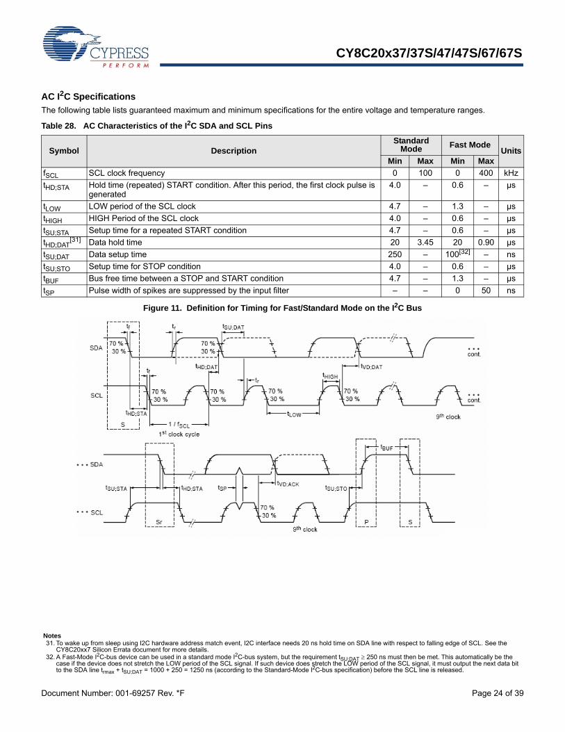
AC I2C Specifications
The following table lists guaranteed maximum and minimum specifications for the entire voltage and temperature ranges.
Figure 11. Definition for Timing for Fast/Standard Mode on the I2C Bus
Table 28. AC Characteristics of the I2C SDA and SCL Pins
Symbol DescriptionStandard
Mode Fast ModeUnits
Min Max Min Max
fSCL SCL clock frequency 0 100 0 400 kHz
tHD;STA Hold time (repeated) START condition. After this period, the first clock pulse is generated
4.0 – 0.6 – µs
tLOW LOW period of the SCL clock 4.7 – 1.3 – µs
tHIGH HIGH Period of the SCL clock 4.0 – 0.6 – µs
tSU;STA Setup time for a repeated START condition 4.7 – 0.6 – µs
tHD;DAT[31] Data hold time 20 3.45 20 0.90 µs
tSU;DAT Data setup time 250 – 100[32] – ns
tSU;STO Setup time for STOP condition 4.0 – 0.6 – µs
tBUF Bus free time between a STOP and START condition 4.7 – 1.3 – µs
tSP Pulse width of spikes are suppressed by the input filter – – 0 50 ns
Notes31. To wake up from sleep using I2C hardware address match event, I2C interface needs 20 ns hold time on SDA line with respect to falling edge of SCL. See the
CY8C20xx7 Silicon Errata document for more details.32. A Fast-Mode I2C-bus device can be used in a standard mode I2C-bus system, but the requirement tSU;DAT 250 ns must then be met. This automatically be the
case if the device does not stretch the LOW period of the SCL signal. If such device does stretch the LOW period of the SCL signal, it must output the next data bit to the SDA line trmax + tSU;DAT = 1000 + 250 = 1250 ns (according to the Standard-Mode I2C-bus specification) before the SCL line is released.
CY8C20x37/37S/47/47S/67/67S
Document Number: 001-69257 Rev. *F Page 25 of 39
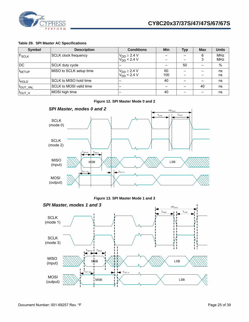
Figure 12. SPI Master Mode 0 and 2
Figure 13. SPI Master Mode 1 and 3
Table 29. SPI Master AC Specifications
Symbol Description Conditions Min Typ Max Units
FSCLK SCLK clock frequency VDD 2.4 VVDD < 2.4 V
––
––
63
MHzMHz
DC SCLK duty cycle – – 50 – %
tSETUP MISO to SCLK setup time VDD 2.4 VVDD < 2.4 V
60100
––
––
nsns
tHOLD SCLK to MISO hold time – 40 – – ns
tOUT_VAL SCLK to MOSI valid time – – – 40 ns
tOUT_H MOSI high time – 40 – – ns
1/FSCLK
TLOW THIGH
TOUT_H
THOLDTSETUP
TOUT_SU
MSB LSB
SPI Master, modes 0 and 2
SCLK(mode 0)
SCLK(mode 2)
MISO(input)
MOSI(output)
1/FSCLK
THIGH TLOW
TOUT_H
THOLDTSETUP
SCLK(mode 1)
SCLK(mode 3)
MISO(input)
MOSI(output)
SPI Master, modes 1 and 3
TOUT_SU
MSB
MSB LSB
LSB
CY8C20x37/37S/47/47S/67/67S
Document Number: 001-69257 Rev. *F Page 26 of 39
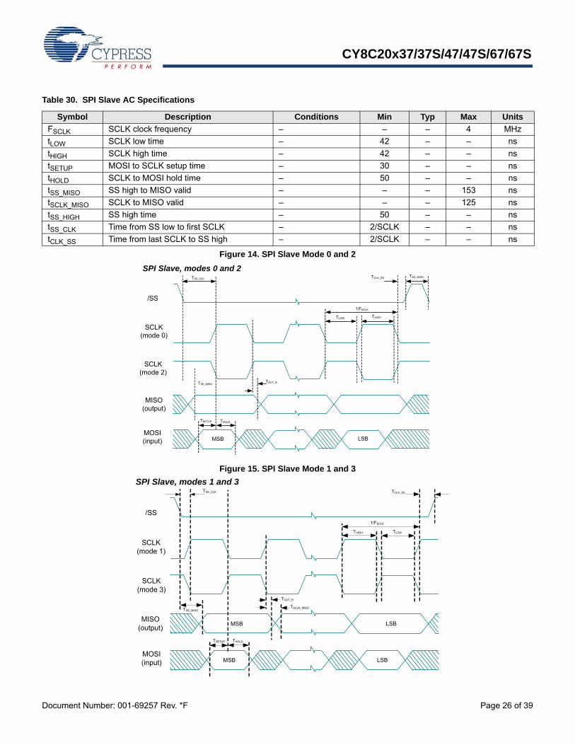
Figure 14. SPI Slave Mode 0 and 2
Figure 15. SPI Slave Mode 1 and 3
Table 30. SPI Slave AC Specifications
Symbol Description Conditions Min Typ Max Units
FSCLK SCLK clock frequency – – – 4 MHz
tLOW SCLK low time – 42 – – ns
tHIGH SCLK high time – 42 – – ns
tSETUP MOSI to SCLK setup time – 30 – – ns
tHOLD SCLK to MOSI hold time – 50 – – ns
tSS_MISO SS high to MISO valid – – – 153 ns
tSCLK_MISO SCLK to MISO valid – – – 125 ns
tSS_HIGH SS high time – 50 – – ns
tSS_CLK Time from SS low to first SCLK – 2/SCLK – – ns
tCLK_SS Time from last SCLK to SS high – 2/SCLK – – ns
TCLK_SS TSS_HIGH
1/FSCLK
TLOW THIGH
TOUT_H
THOLDTSETUP
TSS_MISO
TSS_CLK
MSB LSB
SPI Slave, modes 0 and 2
/SS
SCLK(mode 0)
SCLK(mode 2)
MISO(output)
MOSI(input)
TCLK_SS
1/FSCLK
THIGH TLOW
TSCLK_MISO
TOUT_H
THOLDTSETUP
TSS_CLK
/SS
SCLK(mode 1)
SCLK(mode 3)
MISO(output)
MOSI(input)
SPI Slave, modes 1 and 3
TSS_MISO
MSB
MSB LSB
LSB
CY8C20x37/37S/47/47S/67/67S
Document Number: 001-69257 Rev. *F Page 27 of 39
Packaging InformationThis section illustrates the packaging specifications for the CY8C20x37/47/67 PSoC device, along with the thermal impedances for each package.
Important Note Emulation tools may require a larger area on the target PCB than the chip’s footprint. For a detailed description ofthe emulation tools’ dimensions, refer to the document titled PSoC Emulator Pod Dimensions at http://www.cypress.com/design/MR10161.
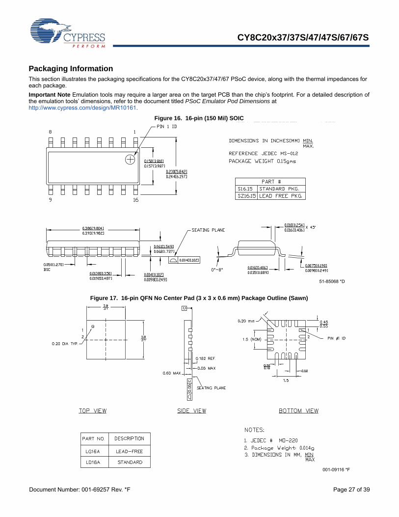
Figure 16. 16-pin (150 Mil) SOIC
Figure 17. 16-pin QFN No Center Pad (3 x 3 x 0.6 mm) Package Outline (Sawn)
51-85068 *D
001-09116 *F
CY8C20x37/37S/47/47S/67/67S
Document Number: 001-69257 Rev. *F Page 28 of 39
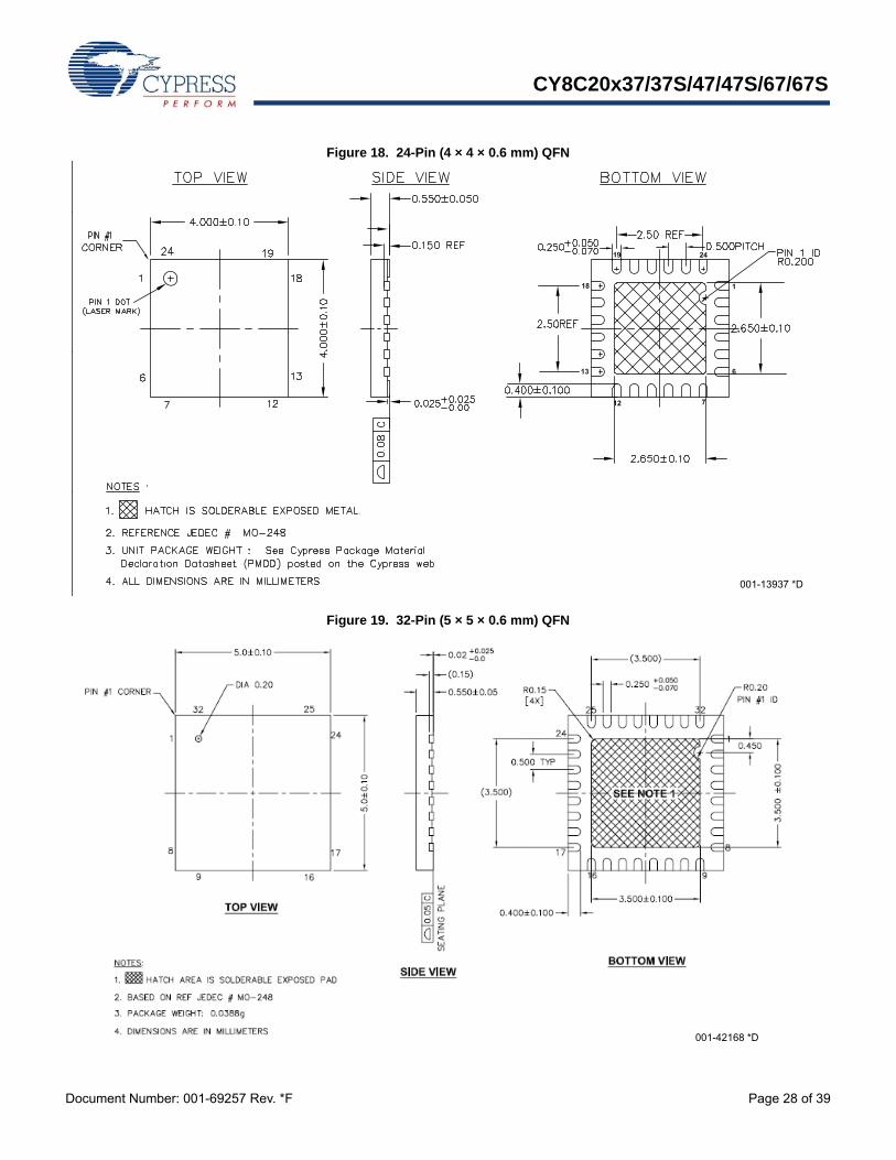
Figure 18. 24-Pin (4 × 4 × 0.6 mm) QFN
Figure 19. 32-Pin (5 × 5 × 0.6 mm) QFN
001-13937 *D
001-42168 *D
CY8C20x37/37S/47/47S/67/67S
Document Number: 001-69257 Rev. *F Page 29 of 39
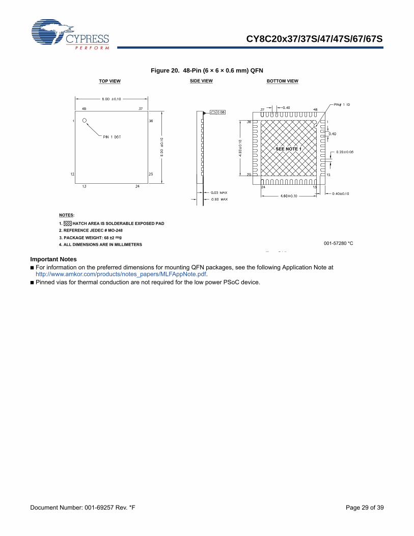
Figure 20. 48-Pin (6 × 6 × 0.6 mm) QFN
Important Notes ■ For information on the preferred dimensions for mounting QFN packages, see the following Application Note at
http://www.amkor.com/products/notes_papers/MLFAppNote.pdf.■ Pinned vias for thermal conduction are not required for the low power PSoC device.
001-57280 *C
CY8C20x37/37S/47/47S/67/67S
Document Number: 001-69257 Rev. *F Page 30 of 39
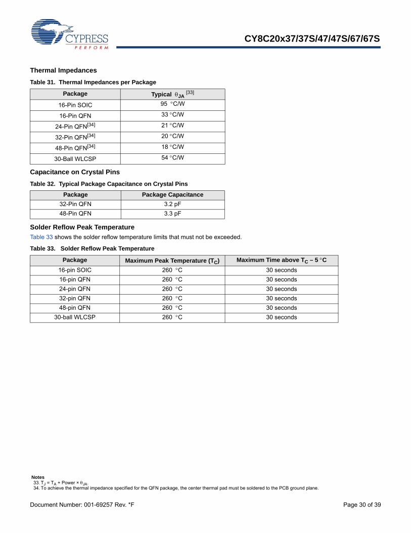
Thermal Impedances
Capacitance on Crystal Pins
Solder Reflow Peak Temperature
Table 33 shows the solder reflow temperature limits that must not be exceeded.
Table 31. Thermal Impedances per Package
Package Typical JA [33]
16-Pin SOIC 95 C/W
16-Pin QFN 33 C/W
24-Pin QFN[34] 21 C/W
32-Pin QFN[34] 20 C/W
48-Pin QFN[34] 18 C/W
30-Ball WLCSP 54 C/W
Table 32. Typical Package Capacitance on Crystal Pins
Package Package Capacitance
32-Pin QFN 3.2 pF
48-Pin QFN 3.3 pF
Table 33. Solder Reflow Peak Temperature
Package Maximum Peak Temperature (TC) Maximum Time above TC – 5 C
16-pin SOIC 260 C 30 seconds
16-pin QFN 260 C 30 seconds
24-pin QFN 260 C 30 seconds
32-pin QFN 260 C 30 seconds
48-pin QFN 260 C 30 seconds
30-ball WLCSP 260 C 30 seconds
Notes33. TJ = TA + Power × JA.34. To achieve the thermal impedance specified for the QFN package, the center thermal pad must be soldered to the PCB ground plane.
CY8C20x37/37S/47/47S/67/67S
Document Number: 001-69257 Rev. *F Page 31 of 39
Development Tool Selection
Software
PSoC Designer™
At the core of the PSoC development software suite isPSoC Designer, used to generate PSoC firmware applications.PSoC Designer is a Microsoft® Windows-based, integrateddevelopment environment for the Programmable System-on-Chip (PSoC) devices. The PSoC Designer IDE and applicationruns on Windows XP and Windows Vista.
This system provides design database management by project,in-system programming support, and built-in support for third-party assemblers and C compilers. PSoC Designer alsosupports C language compilers developed specifically for thedevices in the PSoC family. PSoC Designer is available free ofcharge at http://www.cypress.com/psocdesigner and includes a free Ccompiler.
PSoC Designer Software Subsystems
You choose a base device to work with and then select differentonboard analog and digital components called user modules thatuse the PSoC blocks. Examples of user modules are ADCs,DACs, Amplifiers, and Filters. You configure the user modulesfor your chosen application and connect them to each other andto the proper pins. Then you generate your project. Thisprepopulates your project with APIs and libraries that you canuse to program your application.
The tool also supports easy development of multipleconfigurations and dynamic reconfiguration. Dynamicreconfiguration allows for changing configurations at run time.Code Generation Tools PSoC Designer supports multiple third-party C compilers and assemblers. The code generation toolswork seamlessly within the PSoC Designer interface and havebeen tested with a full range of debugging tools. The choice isyours.
Assemblers. The assemblers allow assembly code to bemerged seamlessly with C code. Link libraries automatically useabsolute addressing or are compiled in relative mode, and linkedwith other software modules to get absolute addressing.
C Language Compilers. C language compilers are availablethat support the PSoC family of devices. The products allow youto create complete C programs for the PSoC family devices. Theoptimizing C compilers provide all the features of C tailored tothe PSoC architecture. They come complete with embeddedlibraries providing port and bus operations, standard keypad anddisplay support, and extended math functionality.
PSoC Programmer
PSoC Programmer is flexible enough and is used on the benchin development and is also suitable for factory programming.PSoC Programmer works either as a standalone programmingapplication or operates directly from PSoC Designer. PSoCProgrammer software is compatible with both PSoC ICE Cubein-circuit Emulator and PSoC MiniProg. PSoC programmer isavailable free of cost at http://www.cypress.com/psocprogrammer.
Development Kits
All development kits are sold at the Cypress Online Store.
Evaluation Tools
All evaluation tools are sold at the Cypress Online Store.
CY3210-MiniProg1
The CY3210-MiniProg1 kit allows you to program PSoC devices through the MiniProg1 programming unit. The MiniProg is a small, compact prototyping programmer that connects to the PC through a provided USB 2.0 cable. The kit includes:
■ MiniProg programming unit
■ MiniEval socket programming and evaluation board
■ 28-pin CY8C29466-24PXI PDIP PSoC device sample
■ 28-pin CY8C27443-24PXI PDIP PSoC device sample
■ PSoC Designer software CD
■ Getting Started guide
■ USB 2.0 cable
CY3210-PSoCEval1
The CY3210-PSoCEval1 kit features an evaluation board and the MiniProg1 programming unit. The evaluation board includes an LCD module, potentiometer, LEDs, and plenty of bread-boarding space to meet all of your evaluation needs. The kit includes:
■ Evaluation board with LCD module
■ MiniProg programming unit
■ Two 28-pin CY8C29466-24PXI PDIP PSoC device samples
■ PSoC Designer software CD
■ Getting Started guide
■ USB 2.0 cable
Device Programmers
All device programmers are purchased from the Cypress Online Store.
CY3216 Modular Programmer
The CY3216 Modular Programmer kit features a modular programmer and the MiniProg1 programming unit. The modular programmer includes three programming module cards and supports multiple Cypress products. The kit includes:
■ Modular programmer base
■ Three programming module cards
■ MiniProg programming unit
■ PSoC Designer software CD
■ Getting Started guide
■ USB 2.0 cable
CY8C20x37/37S/47/47S/67/67S
Document Number: 001-69257 Rev. *F Page 32 of 39
CY3207ISSP In-System Serial Programmer (ISSP)
The CY3207ISSP is a production programmer. It includesprotection circuitry and an industrial case that is more robust thanthe MiniProg in a production-programming environment.
Note CY3207ISSP needs special software and is not compatiblewith PSoC Programmer. The kit includes:
■ CY3207 programmer unit
■ PSoC ISSP software CD
■ 110 ~ 240 V power supply, Euro-Plug adapter
■ USB 2.0 cable
Accessories (Emulation and Programming)
Third Party Tools
Several tools have been specially designed by the following third-party vendors to accompany PSoC devices during development and production. Specific details for each of these tools can be found at http://www.cypress.com under Documentation > Evaluation Boards.
Build a PSoC Emulator into Your Board
For details on how to emulate your circuit before going to volume production using an on-chip debug (OCD) non-production PSoC device, see the Application Note Debugging - Build a PSoC Emulator into Your Board – AN2323.
Table 34. Emulation and Programming Accessories
Part Number Pin Package Flex-Pod Kit[35] Foot Kit[36] Adapter[37]
CY8C20237-24LKXI 16 QFN CY3250-20246QFN CY3250-20246QFN-POD See note 34
CY8C20247-24LKXI 16 QFN CY3250-20246QFN CY3250-20246QFN-POD See note 37
CY8C20337-24LQXI 24 QFN CY3250-20346QFN CY3250-20346QFN-POD See note 34
CY8C20347-24LQXI 24 QFN CY3250-20346QFN CY3250-20346QFN-POD See note 37
CY8C20437-24LQXI 32 QFN CY3250-20466QFN CY3250-20466QFN-POD See note 34
CY8C20447-24LQXI 32 QFN CY3250-20466QFN CY3250-20466QFN-POD See note 37
CY8C20467-24LQXI 32 QFN CY3250-20466QFN CY3250-20466QFN-POD See note 37
CY8C20637-24LQXI 48 QFN CY3250-20666QFN CY3250-20666QFN-POD See note 37
CY8C20647-24LQXI 48 QFN CY3250-20666QFN CY3250-20666QFN-POD See note 37
CY8C20667-24LQXI 48 QFN CY3250-20666QFN CY3250-20666QFN-POD See note 37
Notes35. Flex-Pod kit includes a practice flex-pod and a practice PCB, in addition to two flex-pods.36. Foot kit includes surface mount feet that can be soldered to the target PCB.37. Programming adapter converts non-DIP package to DIP footprint. Specific details and ordering information for each of the adapters can be found at
http://www.emulation.com.
CY8C20x37/37S/47/47S/67/67S
Document Number: 001-69257 Rev. *F Page 33 of 39
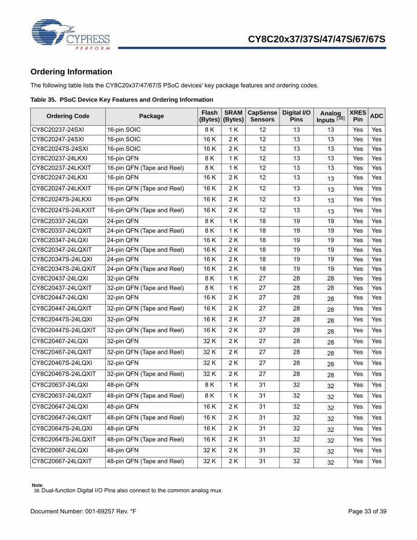
Ordering Information
The following table lists the CY8C20x37/47/67/S PSoC devices' key package features and ordering codes.
Note38. Dual-function Digital I/O Pins also connect to the common analog mux.
Table 35. PSoC Device Key Features and Ordering Information
Ordering Code Package Flash (Bytes)
SRAM (Bytes)
CapSense Sensors
Digital I/O Pins
Analog Inputs [38]
XRES Pin ADC
CY8C20237-24SXI 16-pin SOIC 8 K 1 K 12 13 13 Yes Yes
CY8C20247-24SXI 16-pin SOIC 16 K 2 K 12 13 13 Yes Yes
CY8C20247S-24SXI 16-pin SOIC 16 K 2 K 12 13 13 Yes Yes
CY8C20237-24LKXI 16-pin QFN 8 K 1 K 12 13 13 Yes Yes
CY8C20237-24LKXIT 16-pin QFN (Tape and Reel) 8 K 1 K 12 13 13 Yes Yes
CY8C20247-24LKXI 16-pin QFN 16 K 2 K 12 13 13 Yes Yes
CY8C20247-24LKXIT 16-pin QFN (Tape and Reel) 16 K 2 K 12 13 13 Yes Yes
CY8C20247S-24LKXI 16-pin QFN 16 K 2 K 12 13 13 Yes Yes
CY8C20247S-24LKXIT 16-pin QFN (Tape and Reel) 16 K 2 K 12 13 13 Yes Yes
CY8C20337-24LQXI 24-pin QFN 8 K 1 K 18 19 19 Yes Yes
CY8C20337-24LQXIT 24-pin QFN (Tape and Reel) 8 K 1 K 18 19 19 Yes Yes
CY8C20347-24LQXI 24-pin QFN 16 K 2 K 18 19 19 Yes Yes
CY8C20347-24LQXIT 24-pin QFN (Tape and Reel) 16 K 2 K 18 19 19 Yes Yes
CY8C20347S-24LQXI 24-pin QFN 16 K 2 K 18 19 19 Yes Yes
CY8C20347S-24LQXIT 24-pin QFN (Tape and Reel) 16 K 2 K 18 19 19 Yes Yes
CY8C20437-24LQXI 32-pin QFN 8 K 1 K 27 28 28 Yes Yes
CY8C20437-24LQXIT 32-pin QFN (Tape and Reel) 8 K 1 K 27 28 28 Yes Yes
CY8C20447-24LQXI 32-pin QFN 16 K 2 K 27 28 28 Yes Yes
CY8C20447-24LQXIT 32-pin QFN (Tape and Reel) 16 K 2 K 27 28 28 Yes Yes
CY8C20447S-24LQXI 32-pin QFN 16 K 2 K 27 28 28 Yes Yes
CY8C20447S-24LQXIT 32-pin QFN (Tape and Reel) 16 K 2 K 27 28 28 Yes Yes
CY8C20467-24LQXI 32-pin QFN 32 K 2 K 27 28 28 Yes Yes
CY8C20467-24LQXIT 32-pin QFN (Tape and Reel) 32 K 2 K 27 28 28 Yes Yes
CY8C20467S-24LQXI 32-pin QFN 32 K 2 K 27 28 28 Yes Yes
CY8C20467S-24LQXIT 32-pin QFN (Tape and Reel) 32 K 2 K 27 28 28 Yes Yes
CY8C20637-24LQXI 48-pin QFN 8 K 1 K 31 32 32 Yes Yes
CY8C20637-24LQXIT 48-pin QFN (Tape and Reel) 8 K 1 K 31 32 32 Yes Yes
CY8C20647-24LQXI 48-pin QFN 16 K 2 K 31 32 32 Yes Yes
CY8C20647-24LQXIT 48-pin QFN (Tape and Reel) 16 K 2 K 31 32 32 Yes Yes
CY8C20647S-24LQXI 48-pin QFN 16 K 2 K 31 32 32 Yes Yes
CY8C20647S-24LQXIT 48-pin QFN (Tape and Reel) 16 K 2 K 31 32 32 Yes Yes
CY8C20667-24LQXI 48-pin QFN 32 K 2 K 31 32 32 Yes Yes
CY8C20667-24LQXIT 48-pin QFN (Tape and Reel) 32 K 2 K 31 32 32 Yes Yes
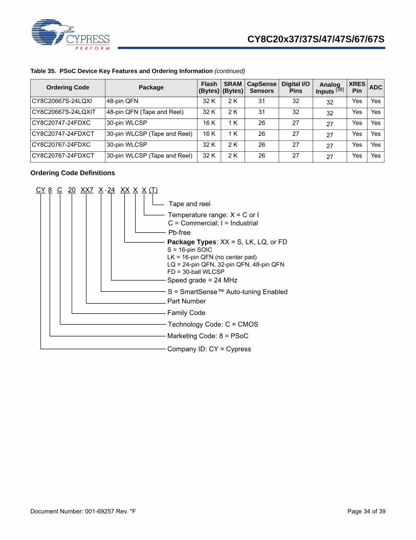
CY8C20x37/37S/47/47S/67/67S
Document Number: 001-69257 Rev. *F Page 34 of 39
Ordering Code Definitions
CY8C20667S-24LQXI 48-pin QFN 32 K 2 K 31 32 32 Yes Yes
CY8C20667S-24LQXIT 48-pin QFN (Tape and Reel) 32 K 2 K 31 32 32 Yes Yes
CY8C20747-24FDXC 30-pin WLCSP 16 K 1 K 26 27 27 Yes Yes
CY8C20747-24FDXCT 30-pin WLCSP (Tape and Reel) 16 K 1 K 26 27 27 Yes Yes
CY8C20767-24FDXC 30-pin WLCSP 32 K 2 K 26 27 27 Yes Yes
CY8C20767-24FDXCT 30-pin WLCSP (Tape and Reel) 32 K 2 K 26 27 27 Yes Yes
Table 35. PSoC Device Key Features and Ordering Information (continued)
Ordering Code PackageFlash
(Bytes)SRAM (Bytes)
CapSense Sensors
Digital I/O Pins
Analog Inputs [38]
XRES Pin ADC
CY
Marketing Code: 8 = PSoC
8 C 20
Technology Code: C = CMOS
Company ID: CY = Cypress
XX7
Family Code
Part Number
X
S = SmartSense™ Auto-tuning Enabled
24
Speed grade = 24 MHz
XX
Package Types: XX = S, LK, LQ, or FD S = 16-pin SOIC LK = 16-pin QFN (no center pad) LQ = 24-pin QFN, 32-pin QFN, 48-pin QFN FD = 30-ball WLCSP
(T)- X X
Pb-free
Temperature range: X = C or IC = Commercial; I = Industrial
Tape and reel
CY8C20x37/37S/47/47S/67/67S
Document Number: 001-69257 Rev. *F Page 35 of 39
AcronymsThe following table lists the acronyms that are used in thisdocument.
Reference Documents
■ Technical reference manual for CY20xx7 devices
■ In-system Serial Programming (ISSP) protocol for 20xx7
■ Host Sourced Serial Programming for 20xx7 devices
Document Conventions
Units of Measure
Table 37 lists all the abbreviations used to measure the PSoCdevices.
Table 36. Acronyms Used in this Document
Acronym DescriptionAC alternating currentADC analog-to-digital converterAPI application programming interfaceCMOS complementary metal oxide semiconductorCPU central processing unitDAC digital-to-analog converterDC direct currentESD electrostatic dischargeFSR full scale rangeGPIO general purpose input/outputI2C inter-integrated circuitICE in-circuit emulatorILO internal low speed oscillatorIMO internal main oscillatorI/O input/outputISSP in-system serial programmingLCD liquid crystal displayLDO low dropout (regulator)LED light-emitting diodeLPC low power comparatorLSB least-significant bitLVD low voltage detectMCU micro-controller unitMIPS million instructions per secondMISO master in slave outMOSI master out slave in MSB most-significant bitOCD on-chip debugPCB printed circuit boardPOR power on resetPSRR power supply rejection ratioPWRSYS power systemPSoC programmable system-on-chipQFN quad flat no-leadSCLK serial I2C clockSDA serial I2C dataSDATA serial ISSP dataSOIC small outline integrated circuitSPI serial peripheral interfaceSRAM static random access memorySS slave selectUSB universal serial busWLCSP wafer level chip scale package
Table 37. Units of Measure
Symbol Unit of Measure°C degree CelsiusdB decibelkHz kilohertzksps kilo samples per secondk kilohmMHz megahertzA microamperes microsecondmA milliamperemm millimeterms millisecondmV millivoltnA nanoamperens nanosecond ohm% percentpF picofaradV voltW watt
CY8C20x37/37S/47/47S/67/67S
Document Number: 001-69257 Rev. *F Page 36 of 39
Numeric Naming
Hexadecimal numbers are represented with all letters in uppercase with an appended lowercase ‘h’ (for example, ‘14h’ or ‘3Ah’).Hexadecimal numbers may also be represented by a ‘0x’ prefix, the C coding convention. Binary numbers have an appendedlowercase ‘b’ (for example, 01010100b’ or ‘01000011b’). Numbers not indicated by an ‘h’, ‘b’, or 0x are decimal.
Glossary
Crosspoint connection Connection between any GPIO combination via analog multiplexer bus.
Differential non linearity Ideally, any two adjacent digital codes correspond to output analog voltages that are exactly one LSB apart. Differential non-linearity is a measure of the worst case deviation from the ideal 1 LSB step.
Hold time Hold time is the time following a clock event during which the data input to a latch or flip-flop must remain stable in order to guarantee that the latched data is correct.
I2C It is a serial multi-master bus used to connect low speed peripherals to MCU.
Integral nonlinearity It is a term describing the maximum deviation between the ideal output of a DAC/ADC and the actual output level.
Latch-up current Current at which the latch-up test is conducted according to JESD78 standard (at 125 degree Celsius)
Power supply rejection ratio (PSRR) The PSRR is defined as the ratio of the change in supply voltage to the corresponding change in output voltage of the device.
Scan The conversion of all sensor capacitances to digital values.
Setup time Period required to prepare a device, machine, process, or system for it to be ready to function.
Signal-to-noise ratio The ratio between a capacitive finger signal and system noise.
SPI Serial peripheral interface is a synchronous serial data link standard.
CY8C20x37/37S/47/47S/67/67S
Document Number: 001-69257 Rev. *F Page 37 of 39
Document History Page
Document Title: CY8C20x37/37S/47/47S/67/67S, 1.8 V CapSense® Controller with SmartSense™ Auto-tuning31 Buttons, 6 SlidersDocument Number: 001-69257
Revision ECN Orig. of Change
Submission Date Description of Change
** 3276782 DST 06/27/2011 New silicon and document
*A 3327230 DST 07/28/2011 Changed 48-pin dimensions to 6 × 6 × 0.6 mm QFNUpdated pins name in Table 3 on page 9 and removed USB column and updated dimensions for 48-pin parts in Table 35 on page 33Updated Figure 20 on page 29Removed ICE and Debugger sections.Removed CY3215 Development Kit and CY3280-20x66 UCC sections.Updated Ordering Information.
*B 3403111 YVA 10/12/2011 Moved status from Advance to Preliminary.Updated Ordering InformationRemoved the row named “48-Pin (6 × 6 mm) QFN (OCD)”.Changed all 48-pin ordering code column from CY8C20XXX-24LTxx to CY8C20XXX-24LQxx.Updated 16-pin SOIC and 16-pin QFN package drawings.
*C 3473317 DST 12/23/2011 Updated Features.Updated Pinouts (Removed PSoC in captions of Figure 2, Figure 3, Figure 4, Figure 6, and Figure 7).Updated DC Chip-Level Specifications under Electrical Specifications (Updated typical value of IDD24 parameter from 3.32 mA to 2.88 mA, updated typical value of IDD12 parameter from 1.86 mA to 1.71 mA, updated typical value of IDD6 parameter from 1.13 mA to 1.16 mA, updated maximum value of ISB0 parameter from 0.50 µA to 1.1 µA, added ISBI2C parameter and its details). Updated DC GPIO Specifications under Electrical Specifications (Added the parameters namely VILLVT3.3, VIHLVT3.3, VILLVT5.5, VIHLVT5.5 and their details in Table 10, added the parameters namely VILLVT2.5, VIHLVT2.5 and their details in Table 11).Added the following sections namely DC I2C Specifications, Shield Driver DC Specifications, and DC IDAC Specifications under Electrical Specifications.Updated AC Chip-Level Specifications (Added the parameter namely tJIT_IMO and its details).Updated Ordering Information (updated Table 35).
*D 3510277 YVA/DST 02/16/2012 Added CY8C20x37/37S/47/47S/67/67S part numbers and changed title to “1.8 V CapSense® Controller with SmartSense™ Auto-tuning 31 Buttons, 6 Sliders”Updated Features.Modified comparator blocks in Logic Block Diagram.Replaced SmartSense with SmartSense auto-tuning.Added CY8C20xx7S part numbers in Pin Definitions.Added footnote for Table 19.Updated Table 20 and Table 21 and added Table 22.Updated F32K1 min value.Updated data hold time min values.Updated CY8C206x7 part information in Table 34.Updated Ordering Information.
*E 3539259 DST 03/01/2012 Changed Datasheet status from Preliminary to Final. Updated all Pinouts to include Driven Shield Output (optional) information. Updated Min value for VLPC Table 14. Updated Offset and Input range in Table 15.
CY8C20x37/37S/47/47S/67/67S
Document Number: 001-69257 Rev. *F Page 38 of 39
*F 3645807 DST/BVI 07/03/2012 Updated FSCLK parameter in the Table 30, “SPI Slave AC Specifications,” on page 26Changed tOUT_HIGH to tOUT_H in Table 29, “SPI Master AC Specifications,” on page 25Updated Features section, “Programmable pin configurations” bullet: ■ Included the following sub-bullet point -
5 mA source current on port 0 and 1 and 1 mA on port 2,3 and 4■ Changed the bullet point “High sink current of 25 mA for each GPIO” to “High
sink current of 25 mA for each GPIO. Total 120 mA maximum sink current per chip”
■ Added “QuietZone™ Controller” bullet and updated “Low power CapSense® block with SmartSense™ auto-tuning” bullet.
Updated package diagrams 001-13937 to *D and 001-57280 to *C revisions.
Document History Page
Document Title: CY8C20x37/37S/47/47S/67/67S, 1.8 V CapSense® Controller with SmartSense™ Auto-tuning31 Buttons, 6 SlidersDocument Number: 001-69257
Document Number: 001-69257 Rev. *F Revised July 3, 2012 Page 39 of 39
All products and company names mentioned in this document may be the trademarks of their respective holders.
CY8C20x37/37S/47/47S/67/67S
© Cypress Semiconductor Corporation, 2011-2012. The information contained herein is subject to change without notice. Cypress Semiconductor Corporation assumes no responsibility for the use ofany circuitry other than circuitry embodied in a Cypress product. Nor does it convey or imply any license under patent or other rights. Cypress products are not warranted nor intended to be used formedical, life support, life saving, critical control or safety applications, unless pursuant to an express written agreement with Cypress. Furthermore, Cypress does not authorize its products for use ascritical components in life-support systems where a malfunction or failure may reasonably be expected to result in significant injury to the user. The inclusion of Cypress products in life-support systemsapplication implies that the manufacturer assumes all risk of such use and in doing so indemnifies Cypress against all charges.
Any Source Code (software and/or firmware) is owned by Cypress Semiconductor Corporation (Cypress) and is protected by and subject to worldwide patent protection (United States and foreign),United States copyright laws and international treaty provisions. Cypress hereby grants to licensee a personal, non-exclusive, non-transferable license to copy, use, modify, create derivative works of,and compile the Cypress Source Code and derivative works for the sole purpose of creating custom software and or firmware in support of licensee product to be used only in conjunction with a Cypressintegrated circuit as specified in the applicable agreement. Any reproduction, modification, translation, compilation, or representation of this Source Code except as specified above is prohibited withoutthe express written permission of Cypress.
Disclaimer: CYPRESS MAKES NO WARRANTY OF ANY KIND, EXPRESS OR IMPLIED, WITH REGARD TO THIS MATERIAL, INCLUDING, BUT NOT LIMITED TO, THE IMPLIED WARRANTIESOF MERCHANTABILITY AND FITNESS FOR A PARTICULAR PURPOSE. Cypress reserves the right to make changes without further notice to the materials described herein. Cypress does notassume any liability arising out of the application or use of any product or circuit described herein. Cypress does not authorize its products for use as critical components in life-support systems wherea malfunction or failure may reasonably be expected to result in significant injury to the user. The inclusion of Cypress’ product in a life-support systems application implies that the manufacturerassumes all risk of such use and in doing so indemnifies Cypress against all charges.
Use may be limited by and subject to the applicable Cypress software license agreement.
Sales, Solutions, and Legal Information
Worldwide Sales and Design Support
Cypress maintains a worldwide network of offices, solution centers, manufacturer’s representatives, and distributors. To find the office closest to you, visit us at Cypress Locations.
Products
Automotive cypress.com/go/automotive
Clocks & Buffers cypress.com/go/clocks
Interface cypress.com/go/interface
Lighting & Power Control cypress.com/go/powerpsoc
cypress.com/go/plc
Memory cypress.com/go/memory
Optical & Image Sensing cypress.com/go/image
PSoC cypress.com/go/psoc
Touch Sensing cypress.com/go/touch
USB Controllers cypress.com/go/USB
Wireless/RF cypress.com/go/wireless
PSoC Solutions
psoc.cypress.com/solutions
PSoC 1 | PSoC 3 | PSoC 5


![Protocolo de TAO S rdoma [Modo de compatibilidad] · Gordon H. Chest 2012: 141: (2) (Suppl) 7S-47S. INDICACIONES INDICACIONES IIII PREVENCIÓN DEL EMBOLISMO DE ORIGEN CARDIACO …](https://img.pdfslide.us/doc/110x75/5b7acf977f8b9a483c8cdd44/protocolo-de-tao-s-rdoma-modo-de-compatibilidad-gordon-h-chest-2012-141.jpg)


![Vector Calculus in Three Dimensions [OLVER, Peter] {37s}](https://img.pdfslide.us/doc/110x75/577cb4631a28aba7118c7194/vector-calculus-in-three-dimensions-olver-peter-37s.jpg)