Embed Size (px)
Citation preview

CY7C027V/027AV/028VCY7C037AV/038V
3.3 V 32 K / 64 K × 16 / 18 Dual-PortStatic RAM
Cypress Semiconductor Corporation • 198 Champion Court • San Jose, CA 95134-1709 • 408-943-2600Document Number: 38-06078 Rev. *G Revised February 5, 2013
3.3 V 32 K / 64 K × 16 / 18 Dual-Port Static RAM
Features
■ True dual-ported memory cells which allow simultaneous access of the same memory location
■ 32K x 16 organization (CY7C027V/027AV [1])
■ 64K x 16 organization (CY7C028V)
■ 32K x 18 organization (CY7C037AV)
■ 64K x 18 organization (CY7C038V)
■ 0.35 micron Complementary metal oxide semiconductor (CMOS) for optimum speed and power
■ High speed access: 15, 20, and 25 ns
■ Low operating power
■ Active: ICC = 115 mA (typical)
■ Standby: ISB3 = 10 A (typical)
■ Fully asynchronous operation
■ Automatic power-down
■ Expandable data bus to 32/36 bits or more using Master/Slave chip select when using more than one device
■ On-chip arbitration logic
■ Semaphores included to permit software handshaking between ports
■ INT flag for port-to-port communication
■ Separate upper-byte and lower-byte control
■ Dual chip enables
■ Pin select for Master or Slave
■ Commercial and Industrial temperature ranges
■ 100-pin Pb-free Thin quad plastic flatpack (TQFP) and 100-pin TQFP
R/WL
CE0LCE1L
OEL
I/O8/9L–I/O15/17LI/O
Control
Address
Decode
A0L–A14/15L
CEL
OEL
R/WL
BUSYL
I/OControl
CEL
InterruptSemaphoreArbitration
SEML
INTL
M/S
UBL
LBL
I/O0L–I/O7/8L
R/WR
CE0RCE1R
OER
I/O8/9L–I/O15/17R
CER
UBR
LBR
I/O0L–I/O7/8R
UBLLBL
Logic Block Diagram
A0L–A14/15LTrue Dual-Ported
RAM Array
A0R–A14/15R
CER
OER
R/WR
BUSYR
SEMR
INTRUBRLBR
Address
DecodeA0R–A14/15R
[2] [2]
[3] [3]
[4] [4]
[5] [5]
[4] [4]15/16
8/9
8/9
15/16
8/9
8/9
15/16 15/16
Notes1. CY7C027V, and CY7C027AV are functionally identical.2. I/O8–I/O15 for x16 devices; I/O9–I/O17 for x18 devices.3. I/O0–I/O7 for x16 devices; I/O0–I/O8 for x18 devices.4. A0–A14 for 32K; A0–A15 for 64K devices.5. BUSY is an output in master mode and an input in slave mode.

CY7C027V/027AV/028VCY7C037AV/038V
Document Number: 38-06078 Rev. *G Page 2 of 24
Contents
Pin Configurations ........................................................... 3Selection Guide ................................................................ 5Pin Definitions .................................................................. 5Architecture ...................................................................... 5Functional Description ..................................................... 5
Write Operation ........................................................... 5Read Operation ........................................................... 6Interrupts ..................................................................... 6Busy ............................................................................ 6Master/Slave ............................................................... 6Semaphore Operation ................................................. 6
Maximum Ratings ............................................................. 7Operating Range ............................................................... 7Electrical Characteristics ................................................. 7Capacitance ...................................................................... 7AC Test Loads and Waveforms ....................................... 8Data Retention Mode ........................................................ 8Timing ................................................................................ 8Switching Characteristics ................................................ 9
Switching Waveforms .................................................... 11Non-Contending Read/Write .......................................... 17Interrupt Operation Example ......................................... 17Semaphore Operation Example .................................... 18Ordering Information ...................................................... 19
32 K × 16 3.3 V Asynchronous Dual-Port SRAM ...... 1964 K × 16 3.3 V Asynchronous Dual-Port SRAM ...... 1932 K × 18 3.3 V Asynchronous Dual-Port SRAM ...... 1964 K × 18 3.3 V Asynchronous Dual-Port SRAM ...... 19Ordering Code Definitions ......................................... 20
Package Diagram ............................................................ 21Acronyms ........................................................................ 22Document Conventions ................................................. 22
Units of Measure ....................................................... 22Document History Page ................................................. 23Sales, Solutions, and Legal Information ...................... 24
Worldwide Sales and Design Support ....................... 24Products .................................................................... 24PSoC Solutions ......................................................... 24
CY7C027V/027AV/028VCY7C037AV/038V
Document Number: 38-06078 Rev. *G Page 3 of 24
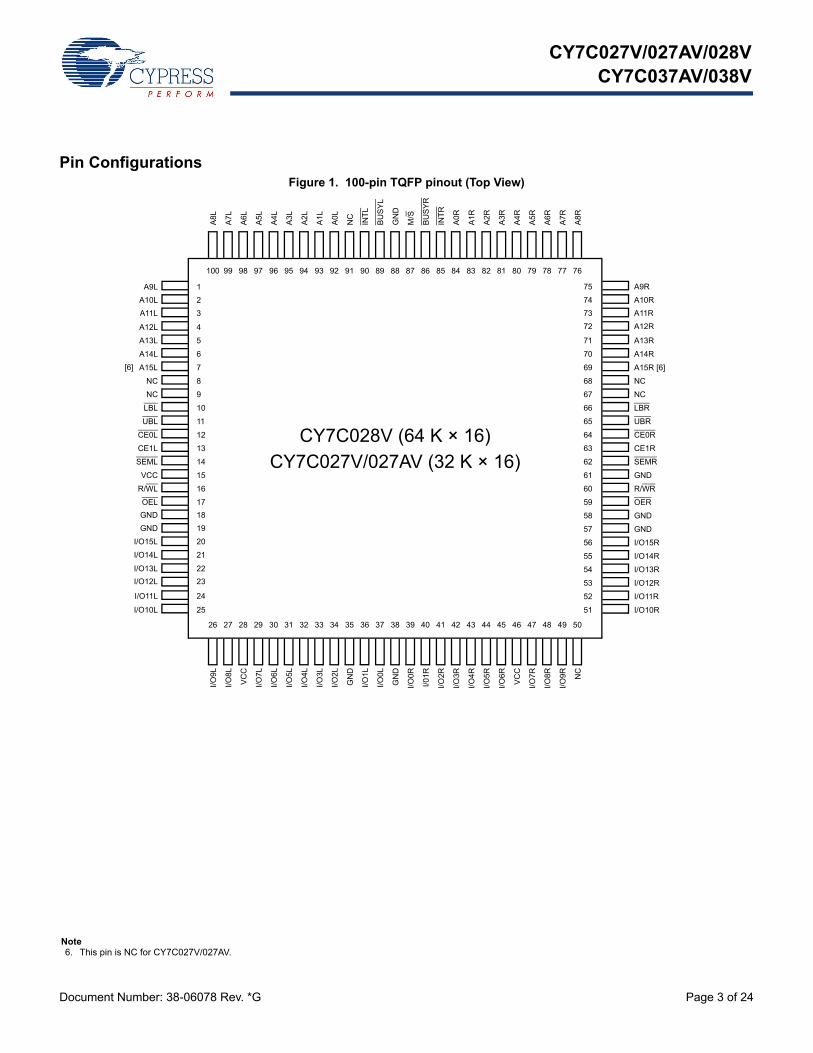
Pin ConfigurationsFigure 1. 100-pin TQFP pinout (Top View)
1
3
2
92 91 90 848587 868889 83 82 81 7678 77798093949596979899100
59
60
61
67
66
64
65
63
62
68
69
70
75
73
74
72
71
A9R
A10R
A11R
A12R
A13R
A14R
UBR
NC
LBR
CE1R
SEMR
OER
GND
NC
A15R
GND
R/WR
GND
I/O15R
I/O14R
I/O13R
I/O12R
I/O11R
I/O10R
CE0R
58
57
56
55
54
53
52
51
CY7C027V/027AV (32 K × 16)
A9L
A10L
A11L
A12L
A13L
A14L
UBL
NC
LBL
CE1L
SEML
OEL
GND
NC
A15L
VCC
R/WL
GND
I/O15L
I/O14L
I/O13L
I/O12L
I/O11L
I/O10L
CE0L
17
16
15
9
10
12
11
13
14
8
7
6
4
5
18
19
20
21
22
23
24
25
A8L
A7L
A6L
A5L
A4L
A3L
INT
L
A1L
NC
GN
D
M/S
A0R
A1R
A0L
A2L
BU
SY
R
INT
R
A2R
A3R
A4R
A5R
A6R
A7R
A8R
BU
SY
L
34 35 36 424139 403837 43 44 45 5048 494746
NC
I/O
9R
I/O
8R
I/O
7R
VC
C
I/O
6R
I/0
1R
I/O
4R
I/O
2R
GN
D
I/O0
L
I/O2
L
I/O3
L
I/O
3R
I/O
5R
I/O1
L
GN
D
I/O4
L
I/O5
L
I/O6
L
I/O7
L
VC
C
I/O8
L
I/O9
L
I/O
0R
3332313029282726
CY7C028V (64 K × 16)
[6] [6]
Note6. This pin is NC for CY7C027V/027AV.

CY7C027V/027AV/028VCY7C037AV/038V
Document Number: 38-06078 Rev. *G Page 4 of 24
Figure 2. 100-pin TQFP pinout (Top View)
Pin Configurations(continued)
1
3
2
92 91 90 848587 868889 83 82 81 7678 77798093949596979899100
59
60
61
67
66
64
65
63
62
68
69
70
75
73
74
72
71
A8R
A9R
A10R
A11R
A12R
A13R
CE0R
A15R
UBR
SEMR
R/WR
GND
I/O17R
LBR
A14R
GND
OER
GND
I/O16R
I/O15R
I/O14R
I/O13R
I/O12R
I/O11R
CE1R
58
57
56
55
54
53
52
51
CY7C037AV (32K x 18)
A9L
A10L
A11L
A12L
A13L
A14L
CE1L
LBL
CE0L
R/WL
OEL
I/O17L
I/O16L
UBL
A15L
VCC
GND
GND
I/O15L
I/O14L
I/O13L
I/O12L
I/O11L
I/O10L
SEML
17
16
15
9
10
12
11
13
14
8
7
6
4
5
18
19
20
21
22
23
24
25
A8L
A7L
A6L
A5L
A4L
A3L
BU
SY
L
A1L
INT
L
GN
D
VC
C
INT
R
A0R
A0L
A2L
M/S
BU
SY
R
A1R
A2R
A3R
A4R
A5R
A6R
A7R
GN
D
34 35 36 424139 403837 43 44 45 5048 494746
I/O10
R
I/O
9R
I/O
8R
I/O
7R
VC
C
I/O
6R
I/01
R
I/O
4R
I/O
2R
GN
D
I/O0
L
I/O2
L
I/O3
L
I/O
3R
I/O
5R
I/O1
L
GN
D
I/O4
L
I/O5
L
I/O6
L
I/O7
L
VC
C
I/O8
L
I/O9
L
I/O
0R
3332313029282726
CY7C038V (64K x 18)
[7]
[7]
Note7. This pin is NC for CY7C037AV.

CY7C027V/027AV/028VCY7C037AV/038V
Document Number: 38-06078 Rev. *G Page 5 of 24
Architecture
The CY7C027V/027AV/028V and CY7037AV/038V consist of anarray of 32K and 64K words of 16 and 18 bits each of dual-portRAM cells, I/O and address lines, and control signals (CE, OE,R/W). These control pins permit independent access for reads or writesto any location in memory. To handle simultaneous writes/reads to thesame location, a BUSY pin is provided on each port. Two interrupt (INT)pins can be utilized for port-to-port communication. Two semaphore(SEM) control pins are used for allocating shared resources. With theM/S pin, the devices can function as a master (BUSY pins are outputs)or as a slave (BUSY pins are inputs). The devices also have anautomatic power down feature controlled by CE. Each port is providedwith its own output enable control (OE), which allows data to be readfrom the device.
Functional Description
The CY7C027V/027AV/028V and CY7037AV/038V are lowpower CMOS 32K, 64K x 16/18 dual-port static RAMs. Variousarbitration schemes are included on the devices to handlesituations when multiple processors access the same piece ofdata. Two ports are provided, permitting independent,asynchronous access for reads and writes to any location inmemory. The devices can be utilized as stand-alone 16/18-bitdual-port static RAMs or multiple devices can be combined to
function as a 32/36-bit or wider master/slave dual-port staticRAM. An M/S pin is provided for implementing 32/36-bit or widermemory applications without the need for separate master andslave devices or additional discrete logic. Application areasinclude interprocessor/multiprocessor designs, communicationsstatus buffering, and dual-port video/graphics memory.
Each port has independent control pins: Chip Enable (CE), Reador Write Enable (R/W), and Output Enable (OE). Two flags areprovided on each port (BUSY and INT). BUSY signals that the port istrying to access the same location currently being accessed by the otherport. The interrupt flag (INT) permits communication between ports orsystems by means of a mail box. The semaphores are used to pass aflag, or token, from one port to the other to indicate that a sharedresource is in use. The semaphore logic is comprised of eight sharedlatches. Only one side can control the latch (semaphore) at any time.Control of a semaphore indicates that a shared resource is in use. Anautomatic power down feature is controlled independently on each portby a chip select (CE) pin.
The CY7C027V/027AV/028V and CY7037AV/038V areavailable in 100-pin Thin Quad Plastic Flatpacks (TQFP).
Write Operation
Data must be set up for a duration of tSD before the rising edge ofR/W to guarantee a valid write. A write operation is controlled by eitherthe R/W pin (see Figure 7) or the CE pin (see Figure 8). Required inputs
Selection Guide
Parameter -15 -20 -25 Unit
Maximum access time 15 20 25 ns
Typical operating current 125 120 115 mA
Typical standby current for ISB1 (Both ports TTL level) 35 35 30 mA
Typical standby current for ISB3 (Both ports CMOS level) 10 10 10 A
Pin DefinitionsLeft Port Right Port Description
CE0L, CE1L CE0R, CE1R Chip Enable (CE is LOW when CE0 VIL and CE1 VIH)
R/WL R/WR Read/Write Enable
OEL OER Output Enable
A0L–A15L A0R–A15R Address (A0–A14 for 32K; A0–A15 for 64K devices)
I/O0L–I/O17L I/O0R–I/O17R Data bus input/output (I/O0–I/O15 for × 16 devices; I/O0–I/O17 for × 18)
SEML SEMR Semaphore Enable
UBL UBR Upper byte select (I/O8–I/O15 for × 16 devices; I/O9–I/O17 for × 18 devices)
LBL LBR Lower byte select (I/O0–I/O7 for × 16 devices; I/O0–I/O8 for × 18 devices)
INTL INTR Interrupt flag
BUSYL BUSYR Busy flag
M/S Master or Slave select
VCC Power
GND Ground
NC No connect

CY7C027V/027AV/028VCY7C037AV/038V
Document Number: 38-06078 Rev. *G Page 6 of 24
for non-contention operations are summarized in Non-ContendingRead/Write on page 17.
If a location is being written to by one port and the opposite portattempts to read that location, a port-to-port flowthrough delaymust occur before the data is read on the output; otherwise thedata read is not deterministic. Data is valid on the port tDDD afterthe data is presented on the other port.
Read Operation
When reading the device, the user must assert both the OE andCE pins. Data is available tACE after CE or tDOE after OE is asserted. Ifthe user wishes to access a semaphore flag, then the SEM pin must beasserted instead of the CE pin, and OE must also be asserted.
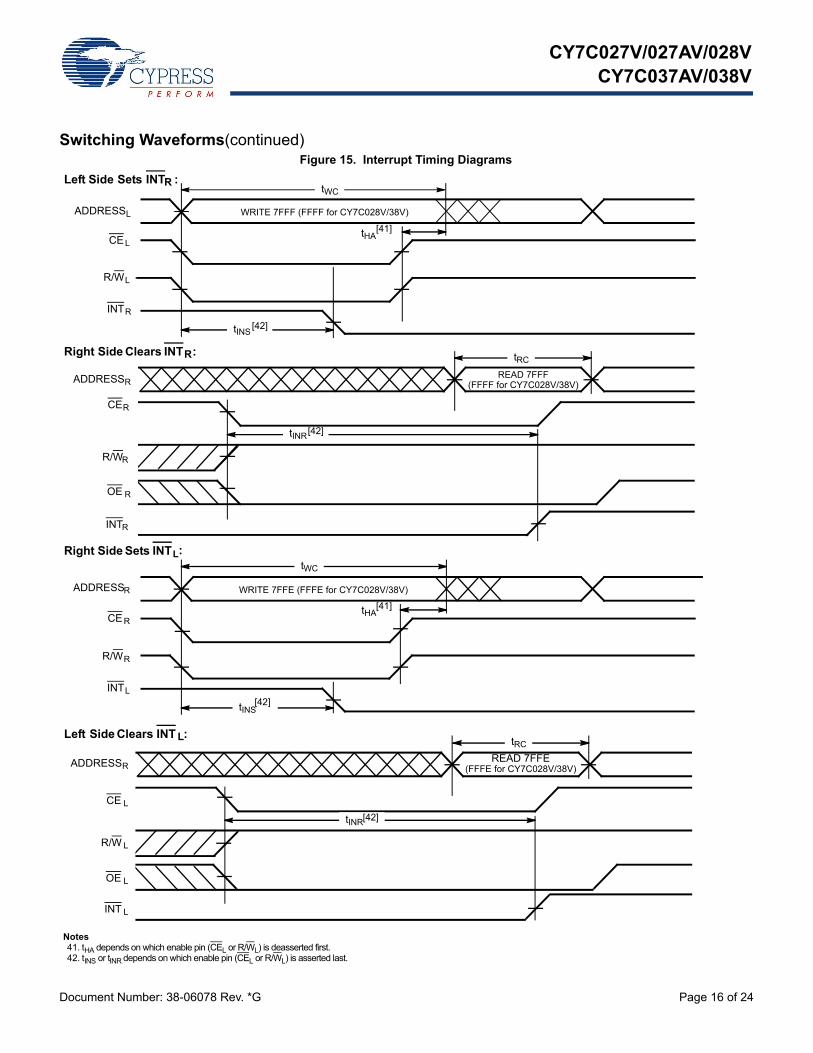
Interrupts
The upper two memory locations may be used for messagepassing. The highest memory location (7FFF for theCY7C027V/037AV/027AV, FFFF for the CY7C028V/38V) is themailbox for the right port and the second-highest memorylocation (7FFE for the CY7C027V/027AV/037AV, FFFE for theCY7C028V/38V) is the mailbox for the left port. When one portwrites to the other port’s mailbox, an interrupt is generated to theowner. The interrupt is reset when the owner reads the contentsof the mailbox. The message is user defined.
Each port can read the other port’s mailbox without resetting theinterrupt. The active state of the busy signal (to a port) preventsthe port from setting the interrupt to the winning port. Also, anactive busy to a port prevents that port from reading its ownmailbox and, thus, resetting the interrupt to it.
If an application does not require message passing, do notconnect the interrupt pin to the processor’s interrupt requestinput pin.
The operation of the interrupts and their interaction with Busy aresummarized in Interrupt Operation Example on page 17.
Busy
The CY7C027V/027AV/028V and CY7037AV/038V provideon-chip arbitration to resolve simultaneous memory locationaccess (contention). If both ports’ CEs are asserted and an addressmatch occurs within tPS of each other, the busy logic determines whichport has access. If tPS is violated, one port definitely gains permission tothe location, but it is not predictable which port gets that permission.BUSY is asserted tBLA after an address match or tBLC after CE is takenLOW.
Master/Slave
A M/S pin is provided to expand the word width by configuring thedevice as either a master or a slave. The BUSY output of the master is
connected to the BUSY input of the slave. This allows the device tointerface to a master device with no external components. Writing toslave devices must be delayed until after the BUSY input has settled(tBLC or tBLA), otherwise, the slave chip may begin a write cycle duringa contention situation. When tied HIGH, the M/S pin allows the deviceto be used as a master and, therefore, the BUSY line is an output. BUSYcan then be used to send the arbitration outcome to a slave.
Semaphore Operation
The CY7C027V/027AV/028V and CY7037AV/038V provideeight semaphore latches, which are separate from the dual-portmemory locations. Semaphores are used to reserve resourcesthat are shared between the two ports.The state of thesemaphore indicates that a resource is in use. For example, ifthe left port wants to request a given resource, it sets a latch bywriting a zero to a semaphore location. The left port then verifiesits success in setting the latch by reading it. After writing to thesemaphore, SEM or OE must be deasserted for tSOP beforeattempting to read the semaphore. The semaphore value is availabletSWRD + tDOE after the rising edge of the semaphore write. If the left portwas successful (reads a zero), it assumes control of the sharedresource, otherwise (reads a one) it assumes the right port has controland continues to poll the semaphore. When the right side has relin-quished control of the semaphore (by writing a one), the left sidesucceeds in gaining control of the semaphore. If the left side no longerrequires the semaphore, a one is written to cancel its request.
Semaphores are accessed by asserting SEM LOW. The SEM pinfunctions as a chip select for the semaphore latches (CE must remainHIGH during SEM LOW). A0–2 represents the semaphore address. OEand R/W are used in the same manner as a normal memory access.When writing or reading a semaphore, the other address pins have noeffect.
When writing to the semaphore, only I/O0 is used. If a zero is writtento the left port of an available semaphore, a one appears at the samesemaphore address on the right port. That semaphore can now only bemodified by the side showing zero (the left port in this case). If the leftport now relinquishes control by writing a one to the semaphore, thesemaphore is set to one for both sides. However, if the right port hadrequested the semaphore (written a zero) while the left port had control,the right port would immediately own the semaphore as soon as the leftport released it. Semaphore Operation Example on page 18 showssample semaphore operations.
When reading a semaphore, all sixteen/eighteen data linesoutput the semaphore value. The read value is latched in anoutput register to prevent the semaphore from changing stateduring a write from the other port. If both ports attempt to accessthe semaphore within tSPS of each other, the semaphore is definitelyobtained by one side or the other, but there is no guarantee which sidecontrols the semaphore.

CY7C027V/027AV/028VCY7C037AV/038V
Document Number: 38-06078 Rev. *G Page 7 of 24
Maximum Ratings
Exceeding maximum ratings may shorten the useful life of thedevice. User guidelines are not tested.
Storage temperature ................................ –65 °C to +150 °C
Ambient temperature with power applied .......................................... –55 °C to +125 °C
Supply voltage to ground potential ..............–0.5 V to +4.6 V
DC voltage applied to outputs in High Z state ........................ –0.5 V to VCC + 0.5 V
DC input voltage [8] ............................. –0.5 V to VCC + 0.5 V
Output current into outputs (LOW) ............................. 20 mA
Static discharge voltage ......................................... > 1100 V
Latch-up current ................................................... > 200 mA
Operating Range
Range Ambient Temperature VCC
Commercial 0 °C to +70 °C 3.3 V 300 mV
Industrial [9] –40 °C to +85 °C 3.3 V 300 mV
Electrical Characteristics
Over the Operating Range
Parameter Description
CY7C027V/027AV/028V/CY7C037AV/CY7C038V
Unit-15 -20 -25
Min Typ Max Min Typ Max Min Typ Max
VOH Output HIGH voltage (VCC = Min., IOH = –4.0 mA) 2.4 – 2.4 – – 2.4 – – V
VOL Output LOW voltage (VCC = Min., IOH = +4.0 mA) – 0.4 – 0.4 – 0.4 V
VIH Input HIGH voltage 2.2 – 2.2 – 2.2 – V
VIL Input LOW voltage – 0.8 – 0.8 – 0.8 V
IIX Input leakage current 5 5 5 5 5 5 A
IOZ Output leakage current –10 10 –10 10 –10 10 A
ICC Operating current (VCC = Max., IOUT = 0 mA) outputs disabled
Commercial – 125 185 – 120 175 – 115 165 mA
Industrial [9] – 140 195 – mA
ISB1 Standby current (Both ports TTL level) CEL & CER VIH, f = fMAX
Commercial 35 50 35 45 30 40 mA
Industrial [9] – 45 55 – mA
ISB2 Standby current (One port TTL level) CEL | CER VIH, f = fMAX
Commercial 80 120 75 110 65 95 mA
Industrial [9] – 85 120 – mA
ISB3 Standby current (Both ports CMOS level) CEL & CER VCC 0.2 V, f = 0
Commercial 10 250 10 250 10 250 A
Industrial [9] – 10 250 – A
ISB4 Standby current (One port CMOS level) CEL | CER VIH, f = fMAX
[10]
Commercial 75 105 70 95 60 80 mA
Industrial [9] – 80 105 – mA
Capacitance
Parameter [11] Description Test Conditions Max Unit
CIN Input capacitance TA = 25 °C, f = 1 MHz, VCC = 3.3 V 10 pF
COUT Output capacitance 10 pF
Notes8. Pulse width < 20 ns.9. Industrial parts are available in CY7C028V and CY7C038V, CY7C027V/027AV only.10. fMAX = 1/tRC = All inputs cycling at f = 1/tRC (except output enable). f = 0 means no address or control lines change. This applies only to inputs at CMOS level standby ISB3.11. Tested initially and after any design or process changes that may affect these parameters.

CY7C027V/027AV/028VCY7C037AV/038V
Document Number: 38-06078 Rev. *G Page 8 of 24
Data Retention Mode
The CY7C027V/027AV/028V and CY7037AV/038V are de-signed with battery backup in mind. Data retention voltage andsupply current are guaranteed over temperature. The followingrules ensure data retention:
1. Chip Enable (CE) must be held HIGH during data retention, within VCC to VCC – 0.2 V
2. CE must be kept between VCC – 0.2 V and 70% of VCC during the power up and power down transitions
3. The RAM can begin operation >tRC after VCC reaches the minimum operating voltage (3.0 V)
AC Test Loads and WaveformsFigure 3. AC Test Loads and Waveforms
3.0V
GND90%
90%10%
3 ns 3 ns
10%
ALL INPUTPULSES
(a) Normal Load (Load 1)
R1 = 590
3.3 V
OUTPUT
R2 = 435 C = 30 pF
VTH = 1.4 V
OUTPUT
C = 30 pF
(b) Thévenin Equivalent (Load 1) (c) Three-State Delay(Load 2)
R1 = 590
R2 = 435
3.3 V
OUTPUT
C = 5 pF
RTH = 250
including scope and jig)
(Used for tLZ, tHZ, tHZWE, & tLZWE
Timing
Parameter Test Conditions [12] Max Unit
ICCDR1 At VCCDR = 2 V 50 A
Data Retention Mode
3.0 V 3.0 VVCC 2.0 V
VCC to VCC – 0.2 V
VCC
CE
tRC
VIH
Note12. CE = VCC, Vin = GND to VCC, TA = 25 C. This parameter is guaranteed but not tested.

CY7C027V/027AV/028VCY7C037AV/038V
Document Number: 38-06078 Rev. *G Page 9 of 24
Switching Characteristics
Over the Operating Range
Parameter [13] Description
CY7C027V/027AV/028V/CY7C037AV/CY7C038V
Unit-15 -20 -25
Min Max Min Max Min Max
Read Cycle
tRC Read cycle time 15 – 20 – 25 – ns
tAA Address to data valid – 15 – 20 – 25 ns
tOHA Output hold from address change 3 – 3 – 3 – ns
tACE[14] CE LOW to data valid – 15 – 20 – 25 ns
tDOE OE LOW to data valid – 10 – 12 – 13 ns
tLZOE[15, 16, 17] OE LOW to Low Z 3 – 3 – 3 – ns
tHZOE[15, 16, 17] OE HIGH to High Z – 10 – 12 – 15 ns
tLZCE[15, 16, 17] CE LOW to Low Z 3 – 3 – 3 – ns
tHZCE[15, 16, 17] CE HIGH to High Z – 10 – 12 – 15 ns
tPU[17] CE LOW to power-up 0 – 0 – 0 – ns
tPD[17] CE HIGH to power-down – 15 – 20 – 25 ns
tABE[14] Byte enable access time – 15 – 20 – 25 ns
Write Cycle
tWC Write cycle time 15 – 20 – 25 – ns
tSCE[14] CE LOW to write end 12 – 16 – 20 – ns
tAW Address valid to write end 12 – 16 – 20 – ns
tHA Address hold from write end 0 – 0 – 0 – ns
tSA[14] Address setup to write start 0 – 0 – 0 – ns
tPWE Write pulse width 12 – 17 – 22 – ns
tSD Data setup to write end 10 – 12 – 15 – ns
tHD Data hold from write end 0 – 0 – 0 – ns
tHZWE[16, 17] R/W LOW to High Z – 10 – 12 – 15 ns
tLZWE[16, 17] R/W HIGH to Low Z 3 – 3 – 3 – ns
tWDD[18] Write pulse to data delay – 30 – 40 – 50 ns
tDDD[18] Write data valid to read data valid – 25 – 30 – 35 ns
Notes13. Test conditions assume signal transition time of 3 ns or less, timing reference levels of 1.5 V, input pulse levels of 0 to 3.0 V, and output loading of the specified IOI/IOH
and 30 pF load capacitance.14. To access RAM, CE=L, UB=L, SEM=H. To access semaphore, CE=H and SEM=L. Either condition must be valid for the entire tSCE time.15. At any given temperature and voltage condition for any given device, tHZCE is less than tLZCE and tHZOE is less than tLZOE.16. Test conditions used are Load 2.17. This parameter is guaranteed by design, but it is not production tested. For information on port-to-port delay through RAM cells from writing port to reading port, refer
to Figure 11.18. tBDD is a calculated parameter and is the greater of tWDD–tPWE (actual) or tDDD–tSD (actual).

CY7C027V/027AV/028VCY7C037AV/038V
Document Number: 38-06078 Rev. *G Page 10 of 24
Busy Timing[19]
tBLA BUSY LOW from address match – 15 – 20 – 20 ns
tBHA BUSY HIGH from address mismatch
– 15 – 20 – 20 ns
tBLC BUSY LOW from CE LOW – 15 – 20 – 20 ns
tBHC BUSY HIGH from CE HIGH – 15 – 16 – 17 ns
tPS Port setup for priority 5 – 5 – 5 – ns
tWB R/W HIGH after BUSY (Slave) 0 – 0 – 0 – ns
tWH R/W HIGH after BUSY HIGH (Slave) 13 – 15 – 17 – ns
tBDD[20] BUSY HIGH to data valid – 15 – 20 – 25 ns
Interrupt Timing[19]
tINS INT set time – 15 – 20 – 20 ns
tINR INT reset time – 15 – 20 – 20 ns
Semaphore Timing
tSOP SEM flag update pulse (OE or SEM)
10 – 10 – 12 – ns
tSWRD SEM flag write to read time 5 – 5 – 5 – ns
tSPS SEM flag contention window 5 – 5 – 5 – ns
tSAA SEM address access time – 15 – 20 – 25 ns
Switching Characteristics(continued)
Over the Operating Range
Parameter [13] Description
CY7C027V/027AV/028V/CY7C037AV/CY7C038V
Unit-15 -20 -25
Min Max Min Max Min Max
Notes19. For information on port-to-port delay through RAM cells from writing port to reading port, refer to Figure 11 waveform.20. tBDD is a calculated parameter and is the greater of tWDD–tPWE (actual) or tDDD–tSD (actual).

CY7C027V/027AV/028VCY7C037AV/038V
Document Number: 38-06078 Rev. *G Page 11 of 24
Switching WaveformsFigure 4. Read Cycle No. 1 (Either Port Address Access) [21, 22, 23]
Figure 5. Read Cycle No. 2 (Either Port CE/OE Access) [21, 24, 25]
Figure 6. Read Cycle No. 3 (Either Port) [21, 23, 24, 25]
tRC
tAAtOHA
DATA VALIDPREVIOUS DATA VALIDDATA OUT
ADDRESS
tOHA
tACE
tLZOE
tDOE
tHZOE
tHZCE
DATA VALID
tLZCE
tPU tPD
ISB
ICC
DATA OUT
OE
CE andLB or UB
CURRENT
UB or LB
DATA OUT
tRC
ADDRESS
tAA tOHA
CE
tLZCE
tABE
tHZCE
tHZCEtACE
tLZCE
Notes21. R/W is HIGH for read cycles.22. Device is continuously selected CE = VIL and UB or LB = VIL. This waveform cannot be used for semaphore reads.23. OE = VIL.24. Address valid prior to or coincident with CE transition LOW.25. To access RAM, CE = VIL, UB or LB = VIL, SEM = VIH. To access semaphore, CE = VIH, SEM = VIL.

CY7C027V/027AV/028VCY7C037AV/038V
Document Number: 38-06078 Rev. *G Page 12 of 24
Figure 7. Write Cycle No. 1: R/W Controlled Timing [26, 27, 28, 29]
Figure 8. Write Cycle No. 2: CE Controlled Timing [26, 27, 28, 34]
Switching Waveforms(continued)
tAW
tWC
tPWE
tHDtSD
tHA
CE
R/W
OE
DATAOUT
DATA IN
ADDRESS
tHZOE
tSA
tHZWE tLZWE
[32]
[32]
[29]
[30,31]
NOTE 33 NOTE 33
tAW
tWC
tSCE
tHDtSD
tHA
CE
R/W
DATA IN
ADDRESS
tSA
[30,31]
Notes26. R/W must be HIGH during all address transitions.27. A write occurs during the overlap (tSCE or tPWE) of a LOW CE or SEM and a LOW UB or LB.28. tHA is measured from the earlier of CE or R/W or (SEM or R/W) going HIGH at the end of write cycle.29. If OE is LOW during a R/W controlled write cycle, the write pulse width must be the larger of tPWE or (tHZWE + tSD) to allow the I/O drivers to turn off and data to be placed on the bus
for the required tSD. If OE is HIGH during an R/W controlled write cycle, this requirement does not apply and the write pulse can be as short as the specified tPWE.30. To access RAM, CE = VIL, SEM = VIH.31. To access upper byte, CE = VIL, UB = VIL, SEM = VIH.
To access lower byte, CE = VIL, LB = VIL, SEM = VIH.32. Transition is measured 500 mV from steady state with a 5 pF load (including scope and jig). This parameter is sampled and not 100% tested.33. During this period, the I/O pins are in the output state, and input signals must not be applied.34. If the CE or SEM LOW transition occurs simultaneously with or after the R/W LOW transition, the outputs remain in the high impedance state.

CY7C027V/027AV/028VCY7C037AV/038V
Document Number: 38-06078 Rev. *G Page 13 of 24
Figure 9. Semaphore Read After Write Timing, Either Side [35]
Figure 10. Timing Diagram of Semaphore Contention [36, 37, 38]
Switching Waveforms(continued)
tSOP
tSAA
VALID ADRESS VALID ADRESS
tHD
DATAIN VALID DATAOUT VALID
tOHA
tAW
tHAtACE
tSOPtSCE
tSD
tSA tPWE
tSWRD tDOE
WRITE CYCLE READ CYCLE
OE
R/W
I/O 0
SEM
0–A 2A
MATCH
tSPS
A0L–A2L
MATCH
R/WL
SEML
A0R–A2R
R/WR
SEM R
Notes35. CE = HIGH for the duration of the above timing (both write and read cycle).36. I/O0R = I/O0L = LOW (request semaphore); CER = CEL = HIGH.37. Semaphores are reset (available to both ports) at cycle start.38. If tSPS is violated, the semaphore is definitely obtained by one side or the other, but which side gets the semaphore is unpredictable.

CY7C027V/027AV/028VCY7C037AV/038V
Document Number: 38-06078 Rev. *G Page 14 of 24
Figure 11. Timing Diagram of Read with BUSY (M/S = HIGH) [39]
Figure 12. Write Timing with Busy Input (M/S = LOW)
Switching Waveforms(continued)
VALID
tDDD
tWDD
MATCH
MATCH
R/WR
DATA INR
DATAOUTL
tWC
ADDRESSR
tPWE
VALID
tSD tHD
ADDRESSL
tPS
tBLA tBHA
tBDDBUSYL
tPWER/W
BUSYtWB tWH
Note39. CEL = CER = LOW.

CY7C027V/027AV/028VCY7C037AV/038V
Document Number: 38-06078 Rev. *G Page 15 of 24
Figure 13. Busy Timing Diagram No. 1 (CE Arbitration) [40]
Figure 14. Busy Timing Diagram No. 2 (Address Arbitration) [40]
Switching Waveforms(continued)
ADDRESS MATCH
tPS
tBLC tBHC
ADDRESS MATCH
tPS
tBLC tBHC
CER ValidFirst:
ADDRESS L,R
BUSYR
CEL
CER
BUSYL
CER
CE L
ADDRESSL,R
CELValid First:
ADDRESS MATCH
tPS
ADDRESSL
BUSYR
ADDRESS MISMATCH
tRC or tWC
tBLA tBHA
ADDRESSR
ADDRESS MATCH ADDRESS MISMATCH
tPS
ADDRESSL
BUSYL
tRC or tWC
tBLA tBHA
ADDRESSR
Right Address Valid First:
Left Address Valid First:
Note40. If tPS is violated, the busy signal is asserted on one side or the other, but there is no guarantee to which side BUSY is asserted.
CY7C027V/027AV/028VCY7C037AV/038V
Document Number: 38-06078 Rev. *G Page 16 of 24
Figure 15. Interrupt Timing Diagrams
Switching Waveforms(continued)
WRITE 7FFF (FFFF for CY7C028V/38V)
tWC
Right Side Clears INTR:
tHA
READ 7FFF
tRC
tINR
WRITE 7FFE (FFFE for CY7C028V/38V)
tWC
Right Side Sets INTL:
Left Side Sets INTR :
Left Side Clears INT L:
READ 7FFE
tINR
tRC
ADDRESSR
CE L
R/W L
INT L
OE L
ADDRESSR
R/WR
CE R
INTL
ADDRESSR
CER
R/WR
INTR
OE R
ADDRESSL
R/WL
CE L
INTR
tINS
tHA
tINS
(FFFF for CY7C028V/38V)
(FFFE for CY7C028V/38V)
[41]
[42]
[42]
[42]
[41]
[42]
Notes41. tHA depends on which enable pin (CEL or R/WL) is deasserted first.42. tINS or tINR depends on which enable pin (CEL or R/WL) is asserted last.

CY7C027V/027AV/028VCY7C037AV/038V
Document Number: 38-06078 Rev. *G Page 17 of 24
Non-Contending Read/WriteInputs Outputs
CE R/W OE UB LB SEM I/O9–I/O17 I/O0–I/O8 Operation
H X X X X H High Z High Z Deselected: Power-down
X X X H H H High Z High Z Deselected: Power-down
L L X L H H Data in High Z Write to upper byte only
L L X H L H High Z Data in Write to lower byte only
L L X L L H Data in Data in Write to both bytes
L H L L H H Data out High Z Read upper byte only
L H L H L H High Z Data out Read lower byte only
L H L L L H Data out Data out Read both bytes
X X H X X X High Z High Z Outputs disabled
H H L X X L Data out Data out Read data in semaphore flag
X H L H H L Data out Data out Read data in semaphore flag
H X X X L Data in Data in Write DIN0 into semaphore flag
X X H H L Data in Data in Write DIN0 into semaphore flag
L X X L X L Not allowed
L X X X L L Not allowed
Interrupt Operation Example
(Assumes BUSYL = BUSYR = HIGH) [43]
Left Port Right Port
Function R/WL CEL OEL A0L–14L INTL R/WR CER OER A0R–14R INTR
Set right INTR flag L L X 7FFF X X X X X L[44]
Reset right INTR flag X X X X X X L L 7FFF H[45]
Set left INTL flag X X X X L[45] L L X 7FFE X
Reset left INTL flag X L L 7FFE H[44] X X X X X
Notes43. A0L–15L and A0R–15R,FFFF/FFFE for the CY7C028V/038V.44. If BUSYL=L, then no change.45. If BUSYR=L, then no change.

CY7C027V/027AV/028VCY7C037AV/038V
Document Number: 38-06078 Rev. *G Page 18 of 24
Semaphore Operation ExampleFunction I/O0–I/O17 Left I/O0–I/O17 Right Status
No action 1 1 Semaphore free
Left port writes 0 to semaphore 0 1 Left port has semaphore token
Right port writes 0 to semaphore 0 1 No change. Right side has no write access to semaphore
Left port writes 1 to semaphore 1 0 Right port obtains semaphore token
Left port writes 0 to semaphore 1 0 No change. Left port has no write access to semaphore
Right port writes 1 to semaphore 0 1 Left port obtains semaphore token
Left port writes 1 to semaphore 1 1 Semaphore free
Right port writes 0 to semaphore 1 0 Right port has semaphore token
Right port writes 1 to semaphore 1 1 Semaphore free
Left port writes 0 to semaphore 0 1 Left port has semaphore token
Left port writes 1 to semaphore 1 1 Semaphore free

CY7C027V/027AV/028VCY7C037AV/038V
Document Number: 38-06078 Rev. *G Page 19 of 24
Ordering Information
32 K × 16 3.3 V Asynchronous Dual-Port SRAM
Speed(ns) Ordering Code
PackageName Package Type
OperatingRange
15 CY7C027V-15AXC A100 100-Pin Pb-free Thin Quad Flat Pack Commercial
CY7C027V-15AXI A100 100-Pin Pb-free Thin Quad Flat Pack Industrial
20 CY7C027V-20AC A100 100-Pin Thin Quad Flat Pack Commercial
CY7C027V-20AXC A100 100-Pin Pb-free Thin Quad Flat Pack Commercial
25 CY7C027V-25AC A100 100-Pin Thin Quad Flat Pack Commercial
CY7C027V-25AXC A100 100-Pin Pb-free Thin Quad Flat Pack Commercial
CY7C027AV-25AXI A100 100-Pin Pb-free Thin Quad Flat Pack Industrial
64 K × 16 3.3 V Asynchronous Dual-Port SRAM
Speed(ns) Ordering Code
PackageName Package Type
OperatingRange
15 CY7C028V-15AXC A100 100-Pin Pb-free Thin Quad Flat Pack Commercial
CY7C028V-15AXI A100 100-Pin Pb-free Thin Quad Flat Pack Industrial
20 CY7C028V-20AXC A100 100-Pin Pb-free Thin Quad Flat Pack Commercial
CY7C028V-20AI A100 100-Pin Thin Quad Flat Pack Industrial
CY7C028V-20AXI A100 100-Pin Pb-free Thin Quad Flat Pack Industrial
25 CY7C028V-25AC A100 100-Pin Thin Quad Flat Pack Commercial
CY7C028V-25AXC A100 100-Pin Pb-free Thin Quad Flat Pack Commercial
32 K × 18 3.3 V Asynchronous Dual-Port SRAM
Speed(ns) Ordering Code
PackageName Package Type
OperatingRange
20 CY7C037AV-20AXC A100 100-Pin Pb-free Thin Quad Flat Pack Commercial
CY7C037AV-20AXI A100 100-Pin Pb-free Thin Quad Flat Pack Industrial
64 K × 18 3.3 V Asynchronous Dual-Port SRAM
Speed(ns) Ordering Code
PackageName Package Type
OperatingRange
20 CY7C038V-20AXI A100 100-Pin Pb-free Thin Quad Flat Pack Industrial

CY7C027V/027AV/028VCY7C037AV/038V
Document Number: 38-06078 Rev. *G Page 20 of 24
Ordering Code Definitions
CY 7C 0X XX
Company ID: CY = Cypress
7C = Dual Port SRAM
Width: 02=x16 or 03=x18
Operating Range C = Commercial I = Industrial
X
Depth: 7=32K or 8=64K
A X
Package: A=TQFP
Speed Grade : 15ns/20ns/25ns
X
X : Pb free (RoHS Compliant)
X
X = V/AV : 3.3 V

CY7C027V/027AV/028VCY7C037AV/038V
Document Number: 38-06078 Rev. *G Page 21 of 24
Package DiagramFigure 16. 100-Pin Pb-Free Thin Plastic Quad Flat Pack (TQFP) A100
51-85048 *G

CY7C027V/027AV/028VCY7C037AV/038V
Document Number: 38-06078 Rev. *G Page 22 of 24
Acronyms Document Conventions
Units of MeasureAcronym Description
CMOS complementary metal oxide semiconductor
I/O input/output
SRAM static random access memory
TQFP thin quad plastic flatpack
Symbol Unit of Measure
°C degree Celsius
MHz mega hertz
µA microamperes
mA milliamperes
mV millivolts
ns nanoseconds
ohms
pF picofarad
V volts
W watts

CY7C027V/027AV/028VCY7C037AV/038V
Document Number: 38-06078 Rev. *G Page 23 of 24
Document History Page
Document Title: CY7C027V/027AV/028V/CY7C037AV/038V, 3.3 V 32 K / 64 K × 16 / 18 Dual-Port Static RAMDocument Number: 38-06078
Rev. ECN No. Orig. of Change
Submission Date Description of Change
** 237626 YDT 6/30/04 Converted data sheet from old spec 38-00670 to conform with new data sheet. Removed cross information from features section
*A 259110 JHX See ECN Added Pb-Free packaging information.
*B 2623540 VKN / PYRS 12/17/08 Added CY7C027VN, CY7C027AV and CY7C037AV partsUpdated Ordering information table
*C 2897217 RAME 03/22/2010 Updated Ordering InformationUpdated Package Diagram
*D 3093542 ADMU 11/25/2010 Removed information on CY7C027VN and CY7C037VUpdated as per new templateAdded Acronyms and Units of Measure tableAdded Ordering Code DefinitionsUpdated all footnotes
*E 3403652 ADMU 10/14/2011 removed pruned parts CY7C027V-25AI, CY7C038V-20AI from Ordering InformationUpdated Package Diagram.
*F 3845411 ADMU 01/29/2013 Updated Ordering Information (Updated part numbers).Updated Package Diagram:spec 51-85048 – Changed revision from *E to *G.
*G 3896090 ADMU 02/05/2013 Updated Ordering Information (Updated part numbers).

Document Number: 38-06078 Rev. *G Revised February 5, 2013 Page 24 of 24
All products and company names mentioned in this document may be the trademarks of their respective holders.
CY7C027V/027AV/028VCY7C037AV/038V
© Cypress Semiconductor Corporation, 2009-2013. The information contained herein is subject to change without notice. Cypress Semiconductor Corporation assumes no responsibility for the use ofany circuitry other than circuitry embodied in a Cypress product. Nor does it convey or imply any license under patent or other rights. Cypress products are not warranted nor intended to be used formedical, life support, life saving, critical control or safety applications, unless pursuant to an express written agreement with Cypress. Furthermore, Cypress does not authorize its products for use ascritical components in life-support systems where a malfunction or failure may reasonably be expected to result in significant injury to the user. The inclusion of Cypress products in life-support systemsapplication implies that the manufacturer assumes all risk of such use and in doing so indemnifies Cypress against all charges.
Any Source Code (software and/or firmware) is owned by Cypress Semiconductor Corporation (Cypress) and is protected by and subject to worldwide patent protection (United States and foreign),United States copyright laws and international treaty provisions. Cypress hereby grants to licensee a personal, non-exclusive, non-transferable license to copy, use, modify, create derivative works of,and compile the Cypress Source Code and derivative works for the sole purpose of creating custom software and or firmware in support of licensee product to be used only in conjunction with a Cypressintegrated circuit as specified in the applicable agreement. Any reproduction, modification, translation, compilation, or representation of this Source Code except as specified above is prohibited withoutthe express written permission of Cypress.
Disclaimer: CYPRESS MAKES NO WARRANTY OF ANY KIND, EXPRESS OR IMPLIED, WITH REGARD TO THIS MATERIAL, INCLUDING, BUT NOT LIMITED TO, THE IMPLIED WARRANTIESOF MERCHANTABILITY AND FITNESS FOR A PARTICULAR PURPOSE. Cypress reserves the right to make changes without further notice to the materials described herein. Cypress does notassume any liability arising out of the application or use of any product or circuit described herein. Cypress does not authorize its products for use as critical components in life-support systems wherea malfunction or failure may reasonably be expected to result in significant injury to the user. The inclusion of Cypress’ product in a life-support systems application implies that the manufacturerassumes all risk of such use and in doing so indemnifies Cypress against all charges.
Use may be limited by and subject to the applicable Cypress software license agreement.
Sales, Solutions, and Legal Information
Worldwide Sales and Design Support
Cypress maintains a worldwide network of offices, solution centers, manufacturer’s representatives, and distributors. To find the office closest to you, visit us at Cypress Locations.
Products
Automotive cypress.com/go/automotive
Clocks & Buffers cypress.com/go/clocks
Interface cypress.com/go/interface
Lighting & Power Control cypress.com/go/powerpsoc
cypress.com/go/plc
Memory cypress.com/go/memory
Optical & Image Sensing cypress.com/go/image
PSoC cypress.com/go/psoc
Touch Sensing cypress.com/go/touch
USB Controllers cypress.com/go/USB
Wireless/RF cypress.com/go/wireless
PSoC Solutions
psoc.cypress.com/solutions
PSoC 1 | PSoC 3 | PSoC 5


![Welcome. [jlikme.blob.core.windows.net]I learned performance on a Commodore 64. @JeremyLikness 8 bits vs. 64 bits •256 vs. 18,446,744,073,709,551,615 (quintillions) •Let 64 K =](https://img.pdfslide.us/doc/110x75/5ec980666ace79356a38eb7a/welcome-i-learned-performance-on-a-commodore-64-jeremylikness-8-bits-vs.jpg)