Embed Size (px)
Citation preview
CY7B952
SST™ SONET/SDH Serial Transceiver
Cypress Semiconductor Corporation • 198 Champion Court • San Jose, CA 95134-1709 • 408-943-2600Document Number: 38-02018 Rev. *E Revised November 9, 2011
SST™ SONET/SDH Serial Transceiver
Features
■ OC-3 Compliant with Bellcore and CCITT (ITU) specifications on:❐ Jitter Generation (<0.01 UI)❐ Jitter Transfer (<130 kHz)❐ Jitter Tolerance
■ SONET/SDH and ATM Compliant
■ Compatible with IGT WAC013, IGT WAC413, and PMC-Sierra PM5343
■ Clock and data recovery from 51.84- or 155.52-MHz datastream
■ 155.52-MHz clock multiplication from 19.44-MHz source
■ 51.84-MHz clock multiplication from 6.48-MHz source
■ 1% frequency agility
■ Line Receiver Inputs: No external buffering required
■ Differential output buffering
■ 100K ECL compatible I/O
■ No output clock “drift” without data transitions
■ Link Status Indication
■ Loop-back testing
■ Single +5 V supply
■ 24-pin SOIC
■ Compatible with fiber-optic modules, coaxial cable, and twisted pair media
■ Power-down options to minimize power or crosstalk
■ Low operating current: <70 mA
■ 0.8 BiCMOS
Functional Description
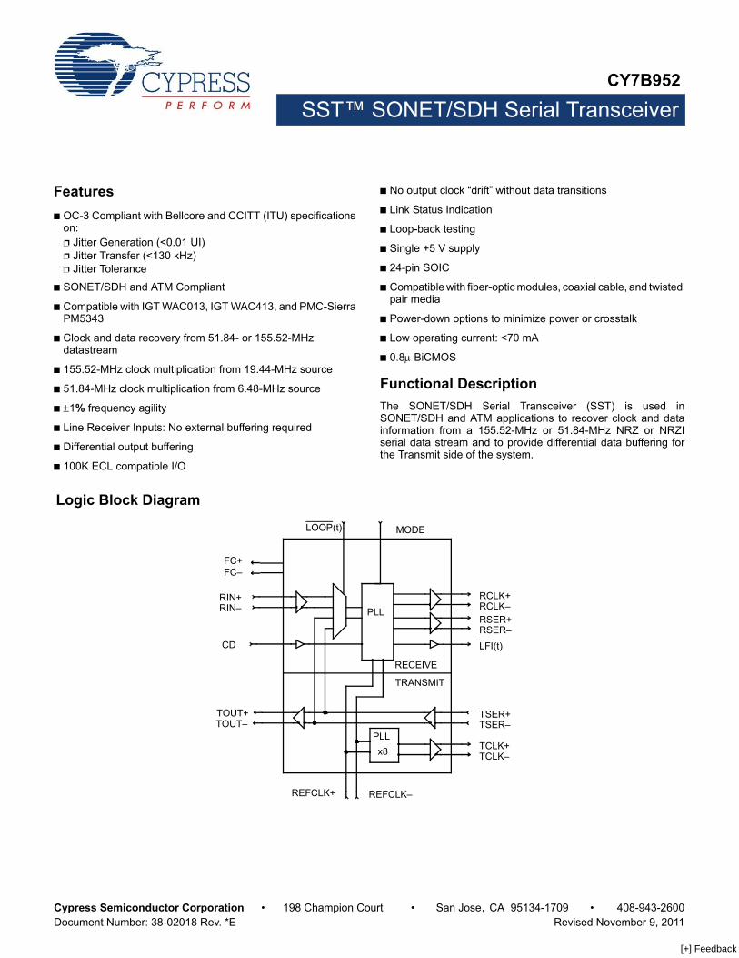
The SONET/SDH Serial Transceiver (SST) is used inSONET/SDH and ATM applications to recover clock and datainformation from a 155.52-MHz or 51.84-MHz NRZ or NRZIserial data stream and to provide differential data buffering forthe Transmit side of the system.
PLL
TCLK–TCLK+
REFCLK+
TRANSMIT
MODE
LFI(t)
FC–FC+
TSER–TSER+
RSER–RSER+RCLK–RCLK+
LOOP(t)
TOUT–TOUT+
x8
RECEIVE
RIN–RIN+
REFCLK–
PLL
CD
Logic Block Diagram
[+] Feedback
CY7B952
Document Number: 38-02018 Rev. *E Page 2 of 16
Contents
Pin Configuration ............................................................. 3SONET/SDH Overhead Processing Application ............ 3Pin Descriptions ............................................................... 4Description ........................................................................ 5
Operating Frequency ................................................... 5Transmit Functions ...................................................... 5Receive Functions ....................................................... 5Carrier Detect (CD) and
Link Fault Indicator (LFI) Functions .................................... 5Loop Back Testing ....................................................... 6SONET-compliant Testing ........................................... 6Power Down Modes .................................................... 6
Applications ...................................................................... 6Maximum Ratings ............................................................. 7Operating Range ............................................................... 7Electrical Characteristics ................................................. 7Capacitance ...................................................................... 9
AC Test Loads and Waveforms ....................................... 9Switching Characteristics .............................................. 10Switching Waveforms for the CY7B952 SONET/SDH Serial Transceiver .............. 11Ordering Information ...................................................... 12
Ordering Code Definitions ......................................... 12Package Diagram ............................................................ 13Acronyms ........................................................................ 14Document Conventions ................................................. 14
Units of Measure ....................................................... 14Document History Page ................................................. 15Sales, Solutions, and Legal Information ...................... 16
Worldwide Sales and Design Support ....................... 16Products .................................................................... 16PSoC Solutions ......................................................... 16
[+] Feedback
CY7B952
Document Number: 38-02018 Rev. *E Page 3 of 16
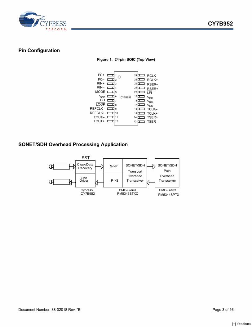
SONET/SDH Overhead Processing Application
Pin Configuration
Figure 1. 24-pin SOIC (Top View)
TCLK+REFCLK+
FC+FC–
RIN+RIN–
MODEVCCCD
LOOPREFCLK–
TOUT–TOUT+
RCLK–RCLK+RSER–RSER+LFIVCCVSSVCCTCLK–
TSER+TSER–
1
2
3
4
5
6
7
8
9
10
11
12
15
16
17
18
19
20
24
23
22
21
13
14
CY7B952
SST
Path
CY7B952Cypress
RecoveryClock/Data
DriverLine
TransportOverhead
Transceiver TransceiverOverhead
SONET/SDH
PMC-SierraPM5343STXC
PMC-Sierra
PM5344SPTX
SONET/SDHS->P
P->S
[+] Feedback
CY7B952
Document Number: 38-02018 Rev. *E Page 4 of 16
Pin Descriptions
Name I/O Description
RIN Differential In Receive Input. This line receiver port connects the receive differential serial input data stream to theinternal Receive PLL. This PLL will recover the embedded clock (RCLK) and data (RSER) informationfor one of two data rates depending on the state of the MODE pin. These inputs can receive very lowamplitude signals and are compatible with all PECL signalling levels. If the RIN inputs are not beingused, connect RIN+ to VCC and RIN– to VSS.
FC Passive Passive Filter Capacitor Connection. These pins are used to connect the external loop dampingcapacitor and resistor for the internal clock and data recovery phase locked loop. A 301K resistorand a non-polar 1 F 10% chip capacitor should be used in parallel for this connection.
RSER ECL Out Recovered Serial Data. These ECL 100K outputs (+5 V referenced) represent the recovered data fromthe input data stream (RIN). This recovered data is aligned with the recovered clock (RCLK) with asampling window compatible with most data processing devices.
RCLK ECL Out Recovered Clock. These ECL 100K outputs (+5 V referenced) represent the recovered clock from theinput data stream (RIN). This recovered clock is used to sample the recovered data (RSER) and hastiming compatible with most data processing devices. If both the RSER and the RCLK are tied to VCCor left unconnected, the entire Receive PLL will be powered down.
CD TTL/ECL In Carrier Detect. This input controls the recovery function of the Receive PLL and can be driven by thecarrier detect output from optical modules or from external transition detection circuitry. When this inputis at an ECL HIGH, the input data stream (RIN) is recovered normally by the Receive PLL. When thisinput is at an ECL LOW, the Receive PLL no longer aligns to RIN, but instead aligns with theREFCLK 8 frequency. Also, the Link Fault Indicator (LFI) will transition LOW, and the recovered dataoutputs (RSER) will remain LOW regardless of the signal level on the Receive data-stream inputs (RIN).When the CD input is at a TTL LOW, the internal transitions detection circuitry is disabled.
LFI TTL Out Link Fault Indicator. This output indicates the status of the input data stream (RIN). It is controlled bythree functions; the Carrier Detect (CD) input, the internal Transition Detector, and the Out of Lock (OOL)detector. The Transition Detector determines if RIN contains enough transitions to be accuratelyrecovered by the Receive PLL. The Out of Lock detector determines if RIN is within the frequency rangeof the Receive PLL. When CD is HIGH and RIN has sufficient transitions and is within the frequencyrange of the Receive PLL, the LFI output will be HIGH. If CD is at an ECL LOW or RIN does not containsufficient transitions or RIN is outside the frequency range of the Receive PLL then the LFI output willbe LOW. If CD is at a TTL LOW then the LFI output will only transition LOW when the frequency of RINis outside the range of the Receive PLL.
TSER Differential In Transmit Serial Data. This line receiver port connects the transmit differential serial input data streamto the TOUT transmit buffers. Depending on the state of the LOOP pin, this input port can also be setup to supply the serial input data stream to the Receive PLL. These inputs can receive very low amplitudesignals and are compatible with all PECL signalling levels. If the TSER inputs are not being used,connect TSER+ to VCC and TSER– to VSS.
TOUT ECL Out Transmit Output. These ECL 100K outputs (+5 V referenced) represent the buffered version of theTransmit data stream (TSER). This Transmit path is used to take weak input signals and rebuffer themto drive low impedance copper media.
REFCLK Diff/TTL In Reference Clock. This input is the clock frequency reference for the clock and data recovery ReceivePLL. REFCLK is multiplied internally by eight and sets the approximate center frequency for the internalReceive PLL to track the incoming bit stream. This input is also multiplied by eight by the frequencymultiplier Transmit PLL to produce the bit rate Transmit Clock (TCLK). REFCLK can be connected toeither a differential PECL or single-ended TTL frequency source. When either REFCLK+ or REFCLK–is at a TTL LOW, the opposite REFCLK signal becomes a TTL level input.
TCLK ECL Out Transmit Clock. These ECL 100K outputs (+5 V referenced) provide the bit rate frequency source forexternal Transmit data processing devices. This output is synthesized by the Transmit PLL and is derivedby multiplying the REFCLK frequency by eight. When this output is turned off, the entire Transmit PLLis powered down. All PECL outputs can be powered down by connecting both outputs to VCC or leavingthem both unconnected.
LOOP TTL In Loop Back Select. This input is used to select the input data stream source that the Receive PLL usesfor clock and data recovery. When the LOOP input is HIGH, the Receive input data stream (RIN) isused for clock and data recovery. When LOOP is LOW, the Transmit input data stream (TSER) is usedby the Receive PLL for clock and data recovery.
[+] Feedback
CY7B952
Document Number: 38-02018 Rev. *E Page 5 of 16
Description
The CY7B952 Serial SONET/SDH Transceiver (SST) is used inSONET/SDH and ATM applications to recover clock and datainformation from a 155.52-MHz or 51.84-MHz NRZ (Non Returnto Zero) or NRZI (Non Return to Zero Invert on ones) serial datastream. This device also provides a bit-rate Transmit clock, froma byte rate source through the use of a frequency multiplier PLL,and differential data buffering for the Transmit side of the system.This device is compliant with relevant SONET/SDHspecifications including OC-3 Bellcore GR-253-Core Issue2,December 1995, ANSI T1X1.6/91-022, and CCITT G958.
Operating Frequency
The SST operates at either of two frequency ranges. The MODEinput selects which of the two frequency ranges the Transmitfrequency multiplier PLL and the Receive clock and datarecovery PLL will operate. The MODE input has three differentfunctional selections. When MODE is connected to VCC, thehighest operating range of the device is selected. A 19.44-MHz1% source must drive the REFCLK input and the two PLLs willmultiply this rate by 8 to provide output clocks that operate at155.52 MHz 1%. When the MODE input is connected to ground(GND), the lowest operating range of the device is selected. A6.48-MHz 1% source must drive the REFCLK inputs and thetwo PLLs will multiply this rate by 8 to provide output clocks thatoperate at 51.84 MHz 1%. When the MODE input is left uncon-nected or forced to approximately VCC/2, the device enters Testmode.
Transmit Functions
The transmit section of the SST contains a PLL that takes aREFCLK input and multiplies it by 8 (REFCLK ×8) to produce aPECL (Pseudo ECL) differential output clock (TCLK). Thetransmitter has two operating ranges that are selectable with thethree-level MODE pin as explained above. The SST Transmitfrequency multiplier PLL allows low-cost byte rate clock sourcesto be used to time the upstream serial data transmitter.
The REFCLK input can be configured three ways. When bothREFCLK+ and REFCLK– are connected to a differential100K-compatible PECL source, the REFCLK input will behaveas a differential PECL input. When either the REFCLK– or theREFCLK+ input is at a TTL LOW, the other REFCLK inputbecomes a TTL-level input allowing it to be connected to alow-cost TTL crystal oscillator. The REFCLK input structure,therefore, can be used as a differential PECL input, a single TTLinput, or as a dual TTL clock multiplexing input.
The Transmit PECL differential input pair (TSER) is buffered bythe SST yielding the differential data outputs (TOUT). Theseoutputs can be used to directly drive transmission media such asPrinted Circuit Board (PCB) traces, optical drivers, twisted pair,or coaxial cable.
Receive Functions
The primary function of the receiver is to recover clock (RCLK)and data (RSER) from the incoming differential PECL datastream (RIN) without the need for external buffering. Thesebuilt-in line receiver inputs, as well as the TSER inputsmentioned above, have a wide common-mode range (2.5 V) andthe ability to receive signals with as little as 50 mV differentialvoltage. They are compatible with all PECL signals and anycopper media.
The clock recovery function is performed using an embeddedPLL. The recovered clock is not only passed to the RCLKoutputs, but also used internally to sample the input serial streamin order to recover the data pattern. The Receive PLL uses theREFCLK input as a byte-rate reference. This input is multipliedby 8 (REFCLK × 8) and is used to improve PLL lock time and toprovide a center frequency for operation in the absence of inputdata stream transitions. The receiver can recover clock and datain two different frequency ranges depending on the state of thethree-level MODE pin as explained earlier. To insure accuratedata and clock recovery, REFCLK8 must be within 1000 ppm ofthe transmit bit rate. The standards, however, specify that theREFCLK ×8 frequency accuracy be within 20–100 ppm.
The FC pins are used to connect an external phase locked loopdamping capacitor and resistor. The capacitor should be a 1 F 10% surface mount devices and the resistor should be a 301K 1% surface mount devices. To minimize noise, the capacitorand the resistor should be placed on the SST side of the printedcircuit board as close to the FC pins as possible.
The Receive PLL is compliant with the OC-3 Bellcore jittergeneration, jitter transfer, and jitter tolerance specifications.
Carrier Detect (CD) and Link Fault Indicator (LFI) Functions
The Link Fault Indicator (LFI) output is a TTL-level output thatindicates the status of the receiver. This output can be used byan external controller for Loss of Signal (LOS), Loss of Frame(LOF), or Out of Frame (OOF) indications. LFI is controlled bythe Carrier Detect input, the internal Transitions Detector, andthe PLL Out of Lock (OOL) circuitry.
The CD input may be driven by external circuitry that ismonitoring the incoming data stream. Optical modules have CD
MODE 3-Level In Frequency Mode Select. This three-level input selects the frequency range for the clock and datarecovery Receive PLL and the frequency multiplier Transmit PLL. When this input is held HIGH the twoPLLs operate at the SONET (SDH) STS-3 (STM-1) line rate of 155.52 MHz. When this input is held LOWthe two PLLs operate at the SONET STS-1 line rate of 51.84 MHz. The REFCLK frequency in bothoperating modes is 1/8 the PLL operating frequency. When the MODE input is left floating or held atVCC/2 the TSER inputs substitute for the internal PLL VCO for use in factory testing.
VCC Power.
VSS Ground.
Pin Descriptions (continued)
Name I/O Description
[+] Feedback
CY7B952
Document Number: 38-02018 Rev. *E Page 6 of 16
outputs that indicate the presence of light on the optical fiber andsome copper based systems use external threshold detectioncircuitry to monitor the incoming data stream. The CD input is a100K PECL compatible signal that should be held HIGH whenthe incoming data stream is valid. When CD is pulled to a PECLLOW (<2.5 V Max.), the LFI output will transition LOW and theReceiver PLL will align itself with the REFCLK8 frequency andthe recovered data outputs (RSER) will remain LOW regardlessof the signal level on the Receive data-stream inputs (RIN).
In addition, the SST has a built-in transitions detector that alsochecks the quality of the incoming data stream. The absence ofdata transition can be caused by a broken transmission media,a broken transmitter, or a problem with the transmit or receivemedia coupling. The SST will detect a quiet link by counting thenumber of bit times that have passed without a data transition. Abit time is defined as the period of RCLK. When 512 bit timeshave passed without a data transition on RIN, LFI will transitionLOW. The receiver will assume that the serial data stream isinvalid and, instead of allowing the RCLK frequency to wanderin the absence of data, the PLL will lock to the REFCLK × 8frequency. This will insure that RCLK is as close to the correctlink operating frequency as the REFCLK accuracy. LFI will bedriven HIGH again and the receiver will recover clock and datafrom the incoming data stream when the transition detectioncircuitry determines that at least 64 transitions have beendetected within 512 bit-times.
The Transition Detector can be turned off by pulling the CD inputto a TTL LOW (<0.8 V). When CD is pulled to a TTL LOW theLFI will only be driven LOW if the incoming data streamfrequency is not within 1000 ppm of the REFCLK ×8 frequency.LFI LOW in this case will only indicate that the Receiver PLL isOut of Lock (OOL). When this pin is left unconnected, an internalpull-down resistor will pull this input to Ground.
Loop Back Testing
The TTL level LOOP pin is used to perform loop-back testing.When LOOP is asserted (held LOW) the Transmitter serial input(TSER) is used by the Receiver PLL for clock and datarecovery. This allows in-system testing to be performed on theentire device except for the differential Transmit drivers (TOUT)and the differential Receiver inputs (RIN). For example, an ATMcontroller can present ATM cells to the input of the ATM cellprocessor and check to see that these same cells are received.When the LOOP input is deasserted (held HIGH) the ReceivePLL is once again connected to the Receiver serial inputs(RIN).
The LOOP feature can also be used in applications where clockand data recovery are to be performed from either of two datastreams. In these systems the LOOP pin is used to selectwhether the TSER or the RIN inputs are used by the ReceivePLL for clock and data recovery.
SONET-compliant Testing
SONET jitter criteria for Bellcore-compliant are specified in threeareas: Jitter transfer, jitter tolerance and jitter generation.
Jitter transfer and jitter tolerance measurements were doneusing sinusoidal jitter applied to the input signal at the maximumamplitude of the jitter tolerance mask for each specific jitterfrequency as specified by the Bellcore GR-253-Core Issue 2,Dec 1995 - SONET Common Generic Criteria.
Power Down Modes
There are several power-down features on the SST. Any of thedifferential output drivers can be powered down by either tyingboth outputs to VCC or by simply leaving them unconnectedwhere internal pull-up resistors will force these outputs to VCC.This will save approximately 4 mA per output pair in addition tothe associated output current. If the TOUT or ROUT outputsare tied to VCC or left unconnected, the Transmit buffer orReceive buffer path respectively will be turned off. If the TCLKoutputs are tied to VCC or left unconnected, the entire TransmitPLL will be powered down.
By leaving both the RCLK and RSER outputs unconnected ortied to VCC, the entire Receive PLL is turned off. Even though theReceive PLL may be turned off, the Link Fault Indicator (LFI) willstill reflect the state of the Carrier Detect (CD) input. This featurecan be used for aggressive power management.
Applications
The SST can provide clock and data recovery as well as outputbuffering for physical layer protocol engines such as those usedin WAN SONET/SDH and ATM applications. The operatingfrequency of the 7B952 is centered around the SONET/SDHSTS-1 rate of 51.84 MHz and the SONET/SDH STS-3/STM-1rate of 155.52 MHz. This device can also be used in data mover,Local Area Network (LAN) applications that operate at thesefrequencies.
In an ATM system, the SST is used to recover clock and datafrom an input SONET/SDH serial data stream for subsequentchips to do serial to parallel conversion, SONET/SDH overheadprocessing, ATM cell processing, and switching. On the Transmitside, ATM cells coming out of a switching matrix goes throughATM cell processing, SONET/SDH overhead processing andparallel to serial conversion before passing to the SST whichbuffers the data stream and drive the transmission media.
In a more generic telecommunications system (SONET/SDHOverhead Processing Application on page 3), the SST is used toprovide clock and data recovery for a pure SONET/SDH systemsuch as a SONET/SDH switch. The SST provides the recoveredclock and data to a serial to parallel converter and SONET/SDHTransport Overhead Processor such as the PMC-Sierra PM5343STXC. The parallel data is then passed to a SONET/SDH PathOverhead Processor such as the PMC-Sierra PM5344 SPTX.
[+] Feedback
CY7B952
Document Number: 38-02018 Rev. *E Page 7 of 16
Maximum Ratings
Exceeding maximum ratings [1] may shorten the useful life of the device. These user guidelines are not tested.
Storage Temperature 65 C to +150 C
Ambient Temperature with Power Applied 55 C to +125 C
Supply Voltage to Ground Potential 0.5 V to +7.0 V
DC Input Voltage 0.5 V to +7.0 V
Output Current into TTL Outputs (LOW) .................... 30 mA
Output Current into ECL Outputs (HIGH) 50 mA
Static Discharge Voltage (per MIL-STD-883, Method 3015) ........................... >2001 V
Latch-up Current ..................................................... >200 mA
Operating Range
Range Ambient Temperature [2] VCC
Commercial 0 C to +70 C 5 V 10%
Electrical Characteristics
Over the Operating Range
Parameter Description Test Condition Min Max Unit
TTL-compatible Input Pins (LOOP, REFCLK+, REFCLK–)
VIHT Input HIGH Voltage 2.0 VCC V
VILT Input LOW Voltage 0.5 0.8 V
IIHT Input HIGH Current REFCLK VIN = VCC +0.5 +200 A
IIHT Input HIGH Current LOOP VIN = VCC 10 +10 A
IILT Input LOW Current REFCLK VIN = 0.0 V 50 +50 A
IILT Input LOW Current LOOP VIN = 0.0 V 500 – A
TTL Compatible Output Pins (LFI)
VOHT Output HIGH Voltage IOH = –2 mA 2.4 – V
VOLT Output LOW Voltage IOL = 4 mA – 0.45 V
IOST Output Short Circuit Current VOUT = 0 V [3] 15 90 mA
ECL Compatible Input Pins (REFCLK, CD, TSER, RIN)
IIHE ECL Input HIGH Current REFCLK/CD VIN = VIHE(MAX) – +250 A
TSER/RIN VIN = VIHE(MAX) – +750 A
IILE[4] ECL Input LOW Current REFCLK/CD VIN = VILE(MIN) +0.5 – A
TSER/RIN VIN = VILE(MIN) 200 – A
VIDIFF Input Differential Voltage TSER/RIN 50 1200 mV
REFCLK 100 1200 mV
VIHE Input High Voltage TSER/RIN – VCC V
REFCLK 3.0 VCC V
CD VCC 1.165 VCC V
VILE Input LOW Voltage TSER/RIN 2.0 – V
REFCLK 2.5 – V
CD (ECL) 2.5 VCC 1.475 V
CD (Disable) 0.5 0.8 V
Notes1. Single Power Supply: The voltage on any input or I/O pin cannot exceed the power pin during power-up.2. TA is the “instant on” case temperature.3. Tested one output at a time, output shorted for less than one second, less than 10% duty cycle.4. Input currents are always positive at all voltages above VCC/2.
[+] Feedback
CY7B952
Document Number: 38-02018 Rev. *E Page 8 of 16
ECL Compatible Output Pins (ROUT, RCLK, RSER, TOUT, TCLK)
VOHE ECL Output HIGH Voltage VCC 1.03 VCC 0.83 V
VOLE ECL Output LOW Voltage T > 0 °C VCC 1.86 VCC 1.62 V
VODIFF Output Differential Voltage 0.6 – V
Three-Level Input Pins (MODE)
VIHH Three-Level Input HIGH VCC 0.75 VCC V
VIMM Three-Level Input MID VCC/2 0.5 VCC/2 + 0.5 V
VILL Three-Level Input LOW 0.0 0.75 V
Operating Current [5]
ICCS Static Operating Current – 38 mA
ICCR Receiver Operating Current – 50 mA
ICCT Transmitter Operating Current – 13 mA
ICCE ECL Pair Operating Current – 7.0 mA
ICC5 Additional Current at 51.84 MHz – 7.0 mA
ICCO Additional Current LFI = LOW – 3 mA
Electrical Characteristics (continued)
Over the Operating Range
Parameter Description Test Condition Min Max Unit
Note5. Total Receiver operating current (assuming that the Transmitter is not activated) can be found by adding ICCS + ICCR + x × ICCE; where x is 2 if the ROUT outputs
are not activated and 3 if they are activated. Total Transmitter operating current (assuming that the Receiver is not activated) can be found by adding ICCS + ICCT + x × ICCE; where x is 1 if the TOUT outputs are not activated and 2 if they are activated. Total device power (assuming that the Transmitter and the Receiver are activated) can be found by adding ICCS + ICCR + ICCT + x × ICCE; where x represents the number of ECL output pairs activated.
[+] Feedback
CY7B952
Document Number: 38-02018 Rev. *E Page 9 of 16
Capacitance
Parameter [6] Description Test Conditions Max Unit
CIN Input Capacitance TA = 25 C, f0 = 1 MHz, VCC = 5.0 V 10 pF
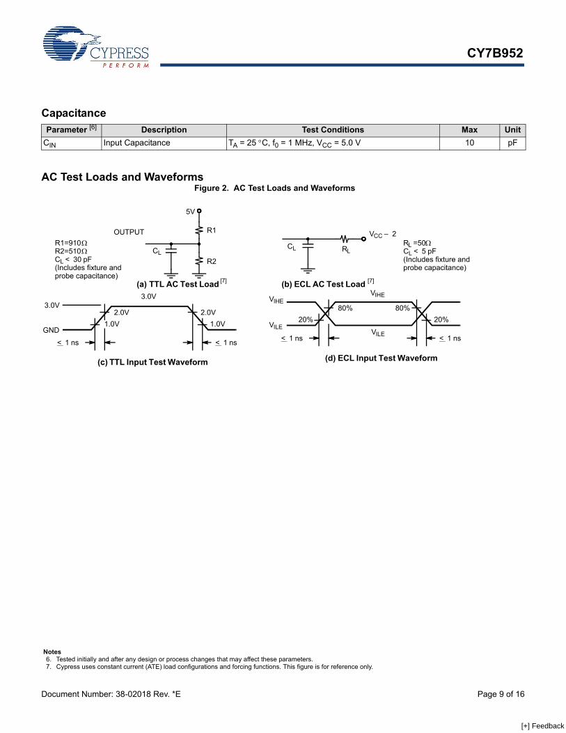
AC Test Loads and WaveformsFigure 2. AC Test Loads and Waveforms
2.0V
1.0V
3.0V
GND
2.0V
1.0V
5V
OUTPUT
(a) TTL AC Test Load (b) ECL AC Test Load
< 1 ns < 1 ns
80%
20%
80%
20%
< 1 ns < 1 ns
(c) TTL Input Test Waveform (d) ECL Input Test Waveform
R1
R2
CLCL RLR1=910R2=510CL < 30 pF(Includes fixture andprobe capacitance)
RL =50CL < 5 pF(Includes fixture andprobe capacitance)
VIHE3.0V
VCC – 2
VIHE
VILEVILE
[7] [7]
Notes6. Tested initially and after any design or process changes that may affect these parameters.7. Cypress uses constant current (ATE) load configurations and forcing functions. This figure is for reference only.
[+] Feedback
CY7B952
Document Number: 38-02018 Rev. *E Page 10 of 16
Switching Characteristics
Over the Operating Range
Parameter Description Min Max Unit
fREF Reference Frequency MODE = LOW 6.41 6.55 MHz
MODE = HIGH 19.24 19.64 MHz
fB Bit Time [8] MODE = LOW 19.5 19.1 ns
MODE = HIGH 6.50 6.40 ns
tODC Output Duty Cycle (TCLK, RCLK) [9] 48 52 %
tRF Output Rise/Fall Time [9] 0.4 1.2 ns
tLOCK PLL Lock Time (RIN transition density 25%) [10] – 3 ms
tRPWH REFCLK Pulse Width HIGH 10 – ns
tRPWL REFCLK Pulse Width LOW 10 – ns
tDV Data Valid 3 – ns
tDH Data Hold 1 – ns
tPD Propagation Delay (RIN to ROUT, TSER to TOUT) [11] – 10 ns
Jitter Generation
Jitter Generation of RX PLL – 0.01 UIrms
f3dB 3 dB Gain Bandwidth of RX PLL (Jitter Transfer Bandwidth)
At 155 MHz – 130 kHz
f3dB 3 dB Gain Bandwidth of RX PLL (Jitter Transfer Bandwidth)
At 52 MHz – 40 kHz
Gpeak Maximum Peaking of RX PLL[12] – 0.1 dB
Notes8. fB is calculated a 1/(fREF8).9. Tested initially and after any design or process changes that may affect these parameters.10. tLOCK is the time needed for transitioning from lock to REFCLK × 8 to lock to data.11. The ECL switching threshold is the differential zero crossing (i.e., the place where + and – signals cross).12. Maximum Peaking is measured using a maximum of 1.2 ns peak to peak duty cycle distortion for RINand applying sinusoidal jitter to the input signal at the maximum
amplitude of the jitter tolerance mask for each specific jitter frequency as specified by the Bellcore GR-253-Core issue 2, Dec 1995 - SONET Common Generic Criteria for OC-3.
[+] Feedback
CY7B952
Document Number: 38-02018 Rev. *E Page 11 of 16
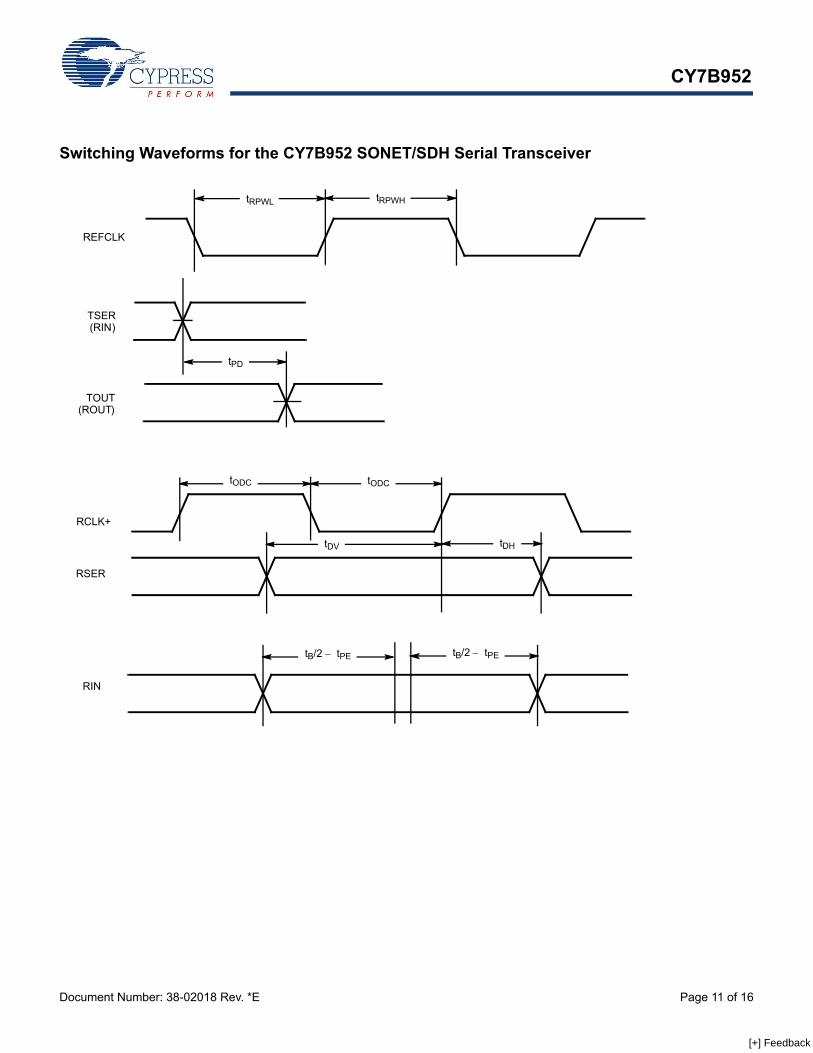
Switching Waveforms for the CY7B952 SONET/SDH Serial Transceiver
REFCLK
tRPWL tRPWH
TSER (RIN )
TOUT (ROUT )
tPD
RCLK+
RSER
tDV tDH
tODC tODC
RIN
tB/2 tPE tB/2 tPE
[+] Feedback
CY7B952
Document Number: 38-02018 Rev. *E Page 12 of 16
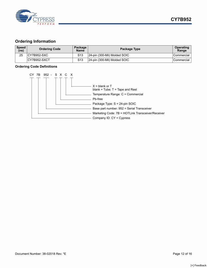
Ordering Code Definitions
Ordering Information
Speed(ns) Ordering Code Package
Name Package Type Operating Range
25 CY7B952-SXC S13 24-pin (300-Mil) Molded SOIC Commercial
CY7B952-SXCT S13 24-pin (300-Mil) Molded SOIC Commercial
X = blank or Tblank = Tube; T = Tape and Reel
Temperature Range: C = Commercial
Pb-free
Package Type: S = 24-pin SOIC
Base part number: 952 = Serial Transceiver
Marketing Code: 7B = HOTLink Transceiver/Receiver
Company ID: CY = Cypress
7BCY C- S X952 X
[+] Feedback
CY7B952
Document Number: 38-02018 Rev. *E Page 13 of 16
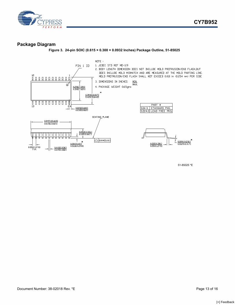
Package DiagramFigure 3. 24-pin SOIC (0.615 × 0.300 × 0.0932 Inches) Package Outline, 51-85025
51-85025 *E
[+] Feedback
CY7B952
Document Number: 38-02018 Rev. *E Page 14 of 16
Acronyms Document Conventions
Units of MeasureAcronym Description
AC alternating current
CD carrier detect
DC direct current
ECL emitter coupled logic
I/O input/output
LFI link fault indicator
PCB printed circuit board
PECL positive emitter coupled logic
PLL phase locked loop
SOIC small-outline integrated circuit
TTL transistor-transistor logic
VCO voltage controlled oscillator
Symbol Unit of Measure
dB decibel
°C degree Celsius
kHz kilohertz
MHz megahertz
µA microampere
µF microfarad
mA milliampere
mV millivolt
ns nanosecond
ohm
% percent
pF picofarad
ppm parts per million
V volt
[+] Feedback
CY7B952
Document Number: 38-02018 Rev. *E Page 15 of 16
Document History Page
Document Title: CY7B952, SST™ SONET/SDH Serial TransceiverDocument Number: 38-02018
Rev. ECN. Issue Date Orig. of Change Description of Change
** 105981 03/28/01 SZV Change from Spec. number: 38-00502 to 38-02018
*A 122206 12/28/02 RBI Add power up requirements to maximum ratings information.
*B 283371 See ECN BCD Removed Preliminary from the data sheet
*C 2896206 03/19/10 CGX Removed obsolete part and added the following parts: CY7B952-SXC and CY7B952-SXCTUpdated package diagram
*D 3092301 11/22/10 SAAC Ordering Information update.Added Ordering Code Definitions.
*E 3434099 11/09/2011 SAAC Updated Package Diagram.Added Acronyms and Units of Measure.Updated in new template.
[+] Feedback
Document Number: 38-02018 Rev. *E Revised November 9, 2011 Page 16 of 16
SUNI is a trademark of PMC-Sierra, Incorporated. SST is a trademark of Cypress Semiconductor Corporation. All products and company names mentioned in this document may be the trademarksof their respective holders.
CY7B952
© Cypress Semiconductor Corporation, 2001-2011. The information contained herein is subject to change without notice. Cypress Semiconductor Corporation assumes no responsibility for the use ofany circuitry other than circuitry embodied in a Cypress product. Nor does it convey or imply any license under patent or other rights. Cypress products are not warranted nor intended to be used formedical, life support, life saving, critical control or safety applications, unless pursuant to an express written agreement with Cypress. Furthermore, Cypress does not authorize its products for use ascritical components in life-support systems where a malfunction or failure may reasonably be expected to result in significant injury to the user. The inclusion of Cypress products in life-support systemsapplication implies that the manufacturer assumes all risk of such use and in doing so indemnifies Cypress against all charges.
Any Source Code (software and/or firmware) is owned by Cypress Semiconductor Corporation (Cypress) and is protected by and subject to worldwide patent protection (United States and foreign),United States copyright laws and international treaty provisions. Cypress hereby grants to licensee a personal, non-exclusive, non-transferable license to copy, use, modify, create derivative works of,and compile the Cypress Source Code and derivative works for the sole purpose of creating custom software and or firmware in support of licensee product to be used only in conjunction with a Cypressintegrated circuit as specified in the applicable agreement. Any reproduction, modification, translation, compilation, or representation of this Source Code except as specified above is prohibited withoutthe express written permission of Cypress.
Disclaimer: CYPRESS MAKES NO WARRANTY OF ANY KIND, EXPRESS OR IMPLIED, WITH REGARD TO THIS MATERIAL, INCLUDING, BUT NOT LIMITED TO, THE IMPLIED WARRANTIESOF MERCHANTABILITY AND FITNESS FOR A PARTICULAR PURPOSE. Cypress reserves the right to make changes without further notice to the materials described herein. Cypress does notassume any liability arising out of the application or use of any product or circuit described herein. Cypress does not authorize its products for use as critical components in life-support systems wherea malfunction or failure may reasonably be expected to result in significant injury to the user. The inclusion of Cypress’ product in a life-support systems application implies that the manufacturerassumes all risk of such use and in doing so indemnifies Cypress against all charges.
Use may be limited by and subject to the applicable Cypress software license agreement.
Sales, Solutions, and Legal Information
Worldwide Sales and Design Support
Cypress maintains a worldwide network of offices, solution centers, manufacturer’s representatives, and distributors. To find the office closest to you, visit us at Cypress Locations.
Products
Automotive cypress.com/go/automotive
Clocks & Buffers cypress.com/go/clocks
Interface cypress.com/go/interface
Lighting & Power Control cypress.com/go/powerpsoc
cypress.com/go/plc
Memory cypress.com/go/memory
Optical & Image Sensing cypress.com/go/image
PSoC cypress.com/go/psoc
Touch Sensing cypress.com/go/touch
USB Controllers cypress.com/go/USB
Wireless/RF cypress.com/go/wireless
PSoC Solutions
psoc.cypress.com/solutions
PSoC 1 | PSoC 3 | PSoC 5
[+] Feedback