Embed Size (px)
Citation preview
CUSTOMIZED OLED DESIGN
FRAUNHOFER INSTITUTE FOR ORGANIC ELECTRONICS, ELECTRON BEAM AND PLASMA TECHNOLOGY FEP
2
3
O R G A N I C E L E C T R O N I C S
ORGANIC ELECTRONICS AT FRAUNHOFER FEP.Fraunhofer FEP combines research and development work for
the production, integration and technology of organic electronic
devices. The focus is on diverse applications entering industrial
production as well as consumer goods applications based on
semiconducting organic materials – e.g. in lighting, information,
automotive, medical, and environmental technologies, as well as
safety technology; really almost every sphere of life.
Processes for flexible OLED lighting at various substrates,
bidirectional OLED microdisplays and ultra-high barrier films for
encapsulation are under development.
Fraunhofer FEP can be partner for customer- and application
orientated research, development and pilot fabrication of novel
module concepts and fabrication methods for these organic
electronic devices.
The institute provides full service – from system design and
technological development to pilot production of small batches
including substrate structuring, deposition technology, encapsu-
lation and system integration. Fraunhofer FEP has an extensive
know-how along the entire value chain for the development of
flexible OLED-modules: from a bare substrate to an integrated
luminaire.
We offer our customers and partners R&D services for each
step of the value chain up to customized layouts on prototy-
pes for small batch series.
4
5
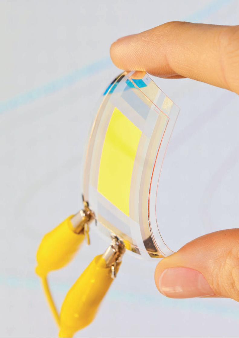
OLED.FLEXIBLEOrganic Light-Emitting Diodes (OLED) offer unique features for
luminaire designs and technical lighting applications. OLED tech-
nology allows white and monochrome emission in nearly every
color. Additionally, OLED can be quasi transparent when switched
off. Next to their appearance another aspect is of importance:
OLED technology is nearly independent of the substrate they
are processed on. Beside rigid glass OLED can be processed on
flexible substrates like polymer webs, metal strips and thin flexible
glass. Such flexible OLED modules allow much more freedom
of design for integration into curved surfaces. In the last years
the Fraunhofer FEP – a wellestablished institute of the European
OLED research – has developed fabrication technologies for OLED
devices by sheet-to-sheet and roll-to-roll processing on different
type of flexible substrates.
Fraunhofer FEP offers the following research and development
topics from concept studies to sample production in the field of
sheet-to-sheet and roll-to-roll fabrication of organic-based devices
on flexible substrates, e.g.:
▪ Optical defect inspection by means of CCD line scan cameras
(pixel resolution 14 μm) or with moveable optical microscope
(point resolution 1 μm)
▪ Lamination of flexible substrates on rigid glass carriers for sheet-
to-sheet processing
▪ Cleaning tests
▪ Vacuum coatings of metal- and metal oxide layers, e.g. TCO
coatings as electrode
▪ Electrode patterning by printing of metal- and dielectric layers or
laser ablation
▪ Vacuum deposition of the OLED layer stack
▪ Slot-die coating for individual layers
▪ Deposition of barrier layers by magnetron sputtering or ALD
▪ Lamination experiments of barrier foils
▪ OLED device integration
▪ System engineering for OLED luminaires
▪ Electro-optical characterization including lifetime measurements
The device development on flexible glass opens the opportunities
of OLED developments for smart signage and lighting integrations,
especially on curved surfaces with the potential of high OLED
lifetime.
F L E X I B L E
Substrate size Polymer film Metal strips Thin flexible glass
Sheet-to-sheet max. 200 × 200 mm²PET, PEN or PI,from 50 μm thickness
Stainless steel, aluminium, etc., any thickness
thickness between 25 μm and 100 μm
Roll-to-roll max. 300 mm widthPET, PEN or PI,from 50 μm thickness
Stainless steel, aluminium, etc. up to 200 μm thick
thickness between 50 μm and 100 μm (sheet substrates up to 300 × 700 mm²)
Substrate types for flexible OLED
6
7
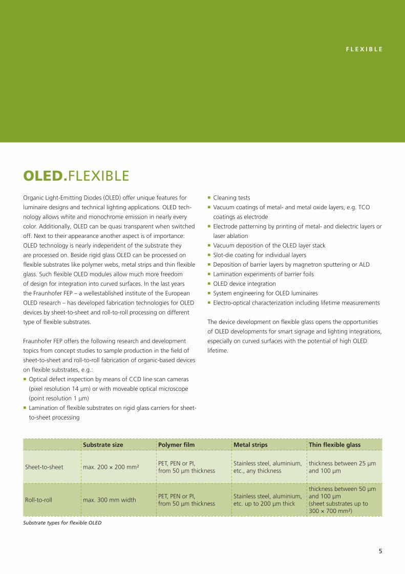
OLED.COLOR-TUNABLEUltrathin light sources with high efficacy and very good color
quality can be realized based on OLED technology on rigid as
well as on flexible substrates. Furthermore OLED technology has
a unique position due to its characteristic as a non-glaring planar
solidstate- lighting source. A characteristic that cannot be realized
with current inorganic LEDs, namely point light sources. A variety
of novel applications appear to be possible based on this existing
technology.
Target of the research and development work at Fraunhofer FEP is
a further broadening of the application fields of OLED technology.
Recently, researchers at Fraunhofer FEP were able to realize a
color-tunable OLED.
The color-tunable OLED is desirable for various lighting applica-
tions e.g. integrated in the interior of trains, cars or planes. It will
be possible to simulate e.g. the ambient lighting conditions of
each time slot of the day: a highly blue light in the morning, white
around noon, and comfortable warm reddish or yellowish light in
the evening.
Furthermore Fraunhofer FEP is working on the integration of
additional functions into the OLED for further niche markets. We
are able to integrate customer specific needs for the development
and implementation of new technologies.
The previous approaches to realize colortunable OLED have been
performed by dividing the lighting plane into extremely small pi-
xels such as display technology or narrow stripes for the realization
of each color (blue, green, red) and driving them with different
voltages. In contrast to this technology Fraunhofer FEP developed
so-called »stacked« OLEDs.
The technology is based on a vertical stacking of OLEDs where
each OLED can be controlled separately. A lateral patterning is not
required. By using this technology, the color of the emitted light
can be tuned continuously. According to the application combi-
nations of two or three colors are possible. Using different process
technologies Fraunhofer FEP was able to achieve the right stack
architecture including the optimized thickness of the individual
OLEDs for an appropriate efficacy.
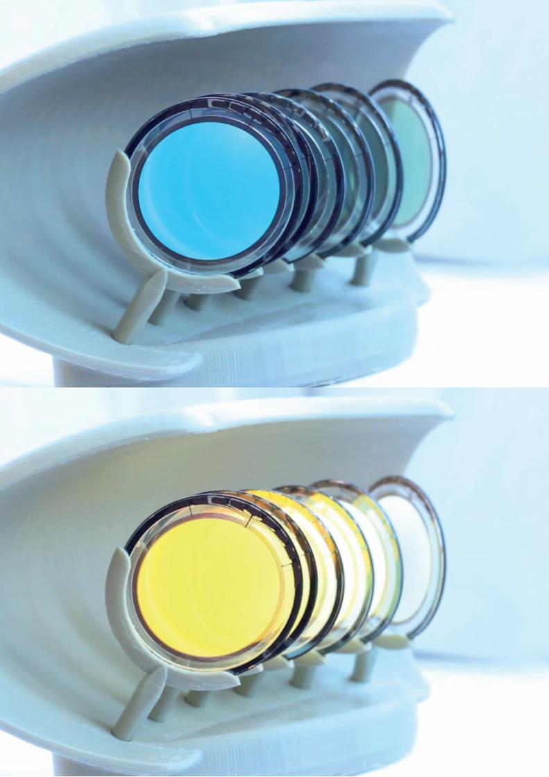
C O L O R - T U N A B L E
Schematic layout of a white-emitting two-color (right) and three-color (left) OLED
Emission spectrum of two-color OLED
8
9
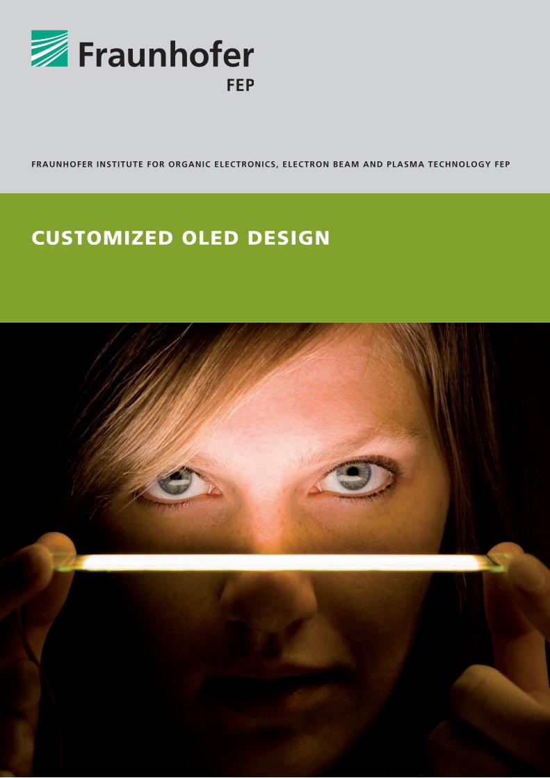
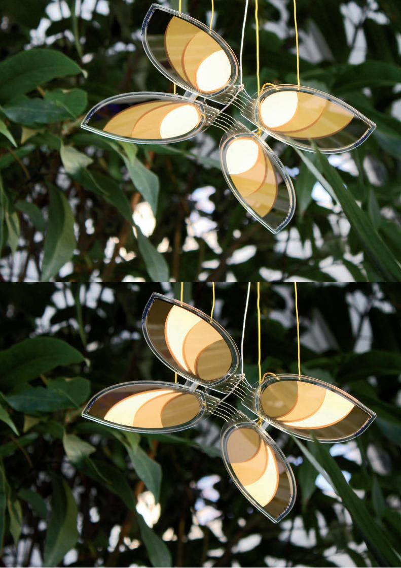
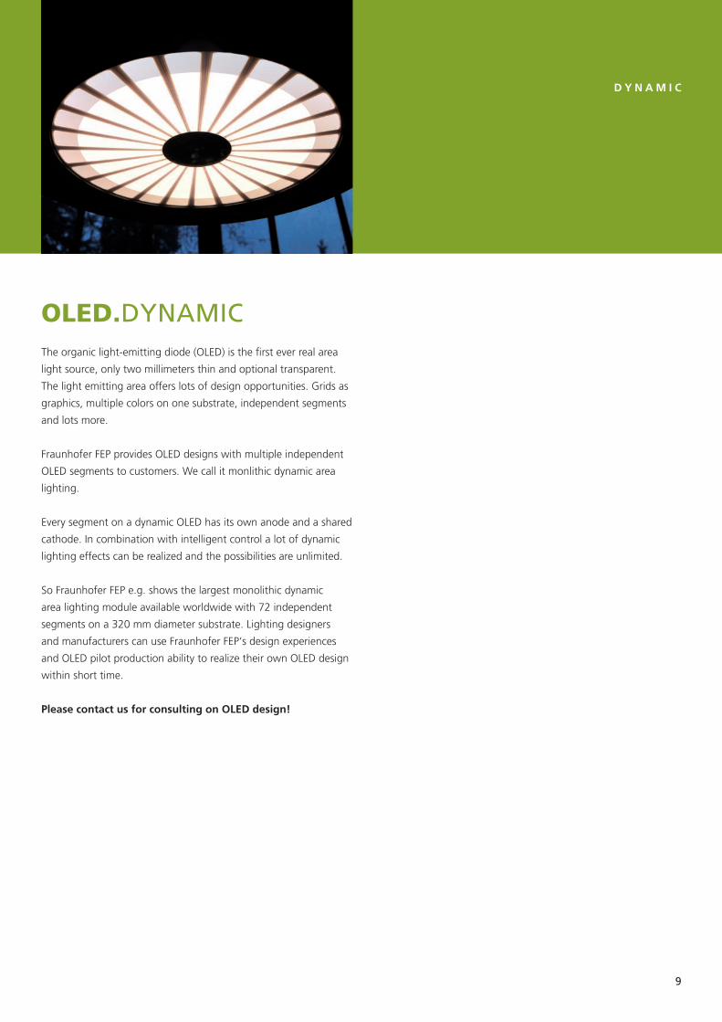
OLED.DYNAMICThe organic light-emitting diode (OLED) is the first ever real area
light source, only two millimeters thin and optional transparent.
The light emitting area offers lots of design opportunities. Grids as
graphics, multiple colors on one substrate, independent segments
and lots more.
Fraunhofer FEP provides OLED designs with multiple independent
OLED segments to customers. We call it monlithic dynamic area
lighting.
Every segment on a dynamic OLED has its own anode and a shared
cathode. In combination with intelligent control a lot of dynamic
lighting effects can be realized and the possibilities are unlimited.
So Fraunhofer FEP e.g. shows the largest monolithic dynamic
area lighting module available worldwide with 72 independent
segments on a 320 mm diameter substrate. Lighting designers
and manufacturers can use Fraunhofer FEP‘s design experiences
and OLED pilot production ability to realize their own OLED design
within short time.
Please contact us for consulting on OLED design!
D Y N A M I C
10
11
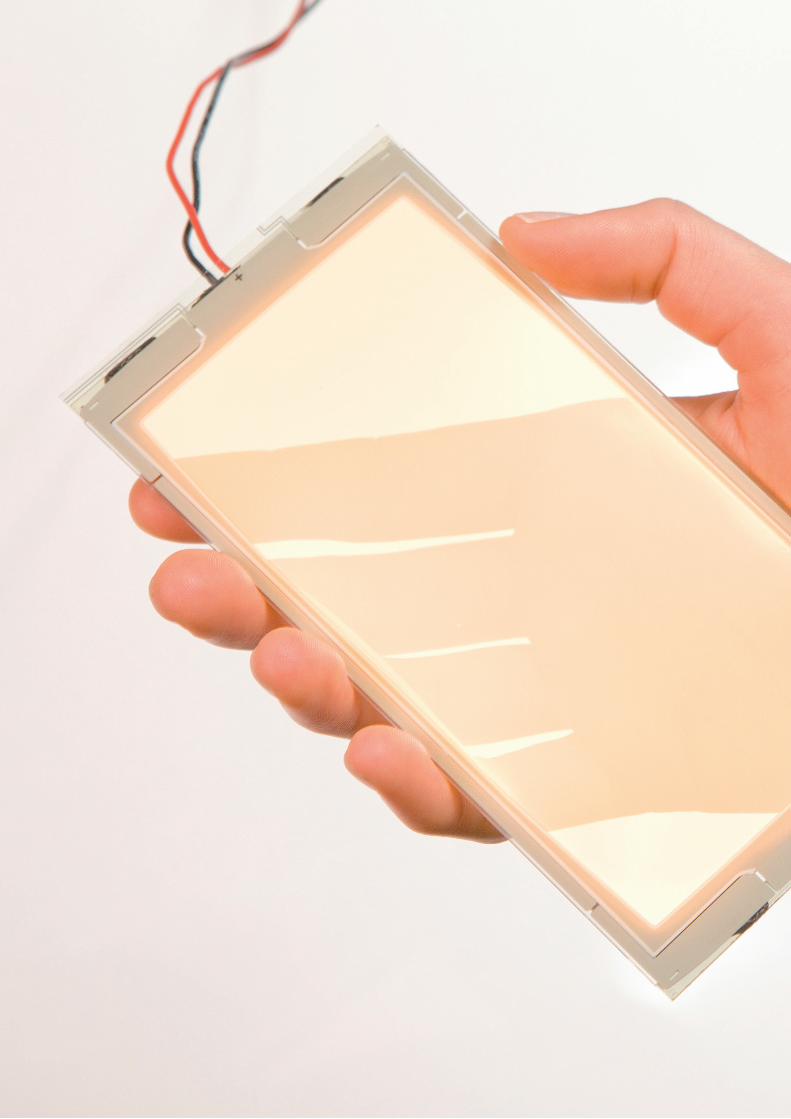
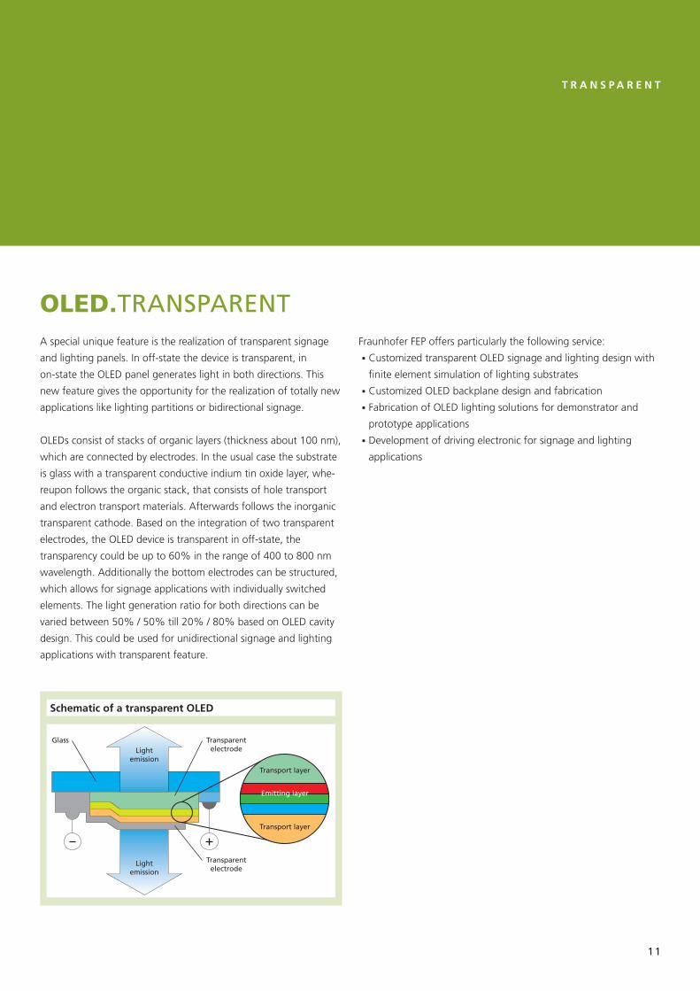
OLED.TRANSPARENTA special unique feature is the realization of transparent signage
and lighting panels. In off-state the device is transparent, in
on-state the OLED panel generates light in both directions. This
new feature gives the opportunity for the realization of totally new
applications like lighting partitions or bidirectional signage.
OLEDs consist of stacks of organic layers (thickness about 100 nm),
which are connected by electrodes. In the usual case the substrate
is glass with a transparent conductive indium tin oxide layer, whe-
reupon follows the organic stack, that consists of hole transport
and electron transport materials. Afterwards follows the inorganic
transparent cathode. Based on the integration of two transparent
electrodes, the OLED device is transparent in off-state, the
transparency could be up to 60% in the range of 400 to 800 nm
wavelength. Additionally the bottom electrodes can be structured,
which allows for signage applications with individually switched
elements. The light generation ratio for both directions can be
varied between 50% / 50% till 20% / 80% based on OLED cavity
design. This could be used for unidirectional signage and lighting
applications with transparent feature.
T R A N S P A R E N T
Fraunhofer FEP offers particularly the following service:
▪ Customized transparent OLED signage and lighting design with
finite element simulation of lighting substrates
▪ Customized OLED backplane design and fabrication
▪ Fabrication of OLED lighting solutions for demonstrator and
prototype applications
▪ Development of driving electronic for signage and lighting
applications
Schematic of a transparent OLED
Lightemission
Transparentelectrode
Glass
Transparentelectrode
Lightemission
Transport layer
Transport layer
Emitting layer
12
13
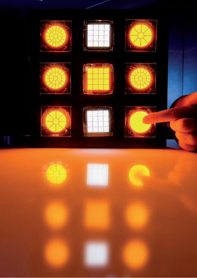
OLED.TOUCH SENSITIVEThe OLED technology is the first real area light source technology.
It overcomes traditional restrictions of point source lighting
technologies (e.g. light bulbs or LED). Their special features could
be the starting point for highly efficient homogenous area light
sources. Beside the area aspects, OLED show also the possibility
for innovative lighting applications, e.g. structured light sources for
signage or color-variable, transparent and flexible light sources.
Due to the OLED construction, the implementation of an
integrated interactive touch interface is possible in a simple way,
an additional unique feature of OLED. This allows the realization
of novel interactive lighting and signage devices without the use
of additional hardware like touch foils which reduces the overall
efficacy.
Organic light-emitting diodes are composed of a stack of organic
layers (thickness about 100 nm), which are connected on both
sides by electrodes. Usually an OLED consists of a glass pane with
a transparent conductive oxide layer, whereupon follow several
layers of organic emitting, hole transport, and electron transport
materials. Afterwards follows the inorganic cathode. Substantial
advantages of the organic luminescence are the chemical variabi-
lity of the organic light-emitting diodes and the thin film system
(extremely low material expense).
OLED are a flat light source, emitting diffuse light from a potential-
ly large active area. OLED do not need light distribution elements,
thus reducing the cost for the whole lighting panel. In contrast,
LEDs are a point source technology which needs light distribution
elements to disperse the light evenly on large areas. Additionally
OLED use low peak brightness on large area, LEDs provide very
high brightness on a small area, which often causes glares.
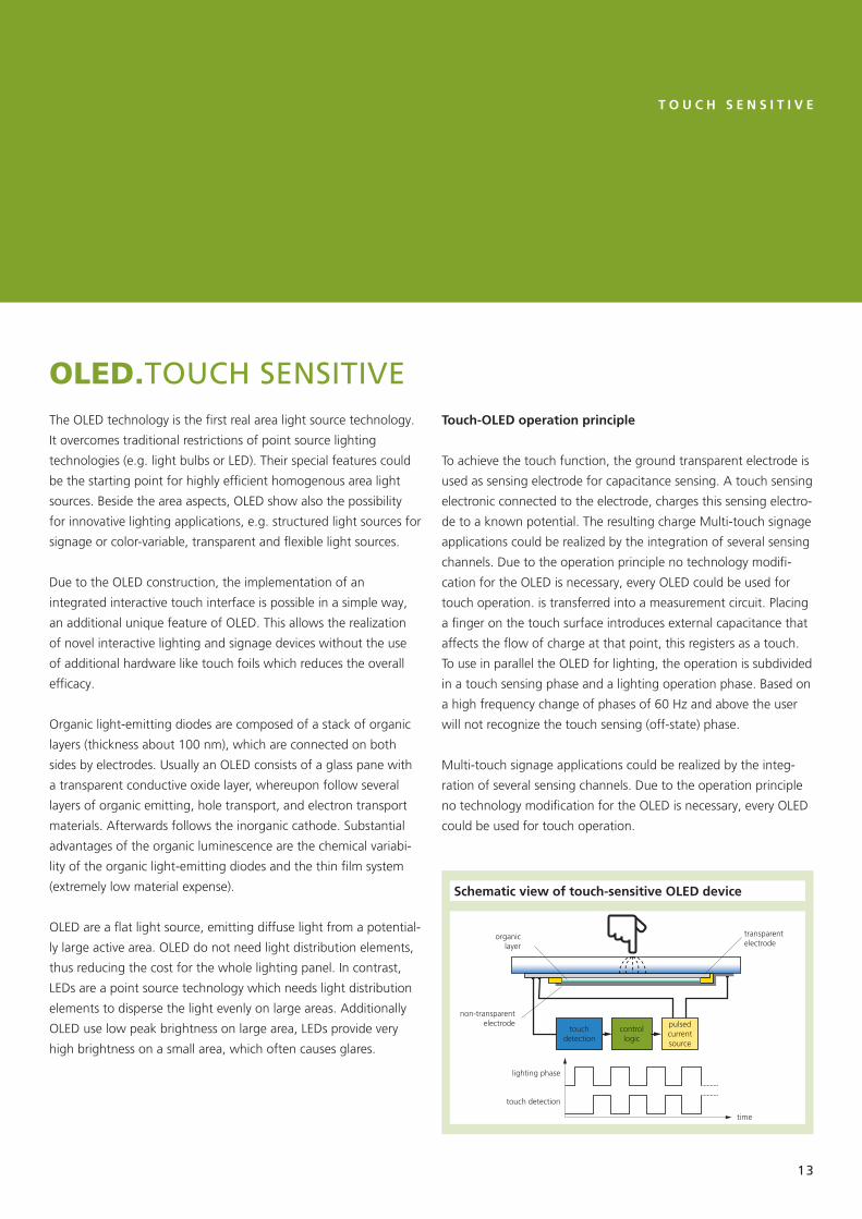
Touch-OLED operation principle
To achieve the touch function, the ground transparent electrode is
used as sensing electrode for capacitance sensing. A touch sensing
electronic connected to the electrode, charges this sensing electro-
de to a known potential. The resulting charge Multi-touch signage
applications could be realized by the integration of several sensing
channels. Due to the operation principle no technology modifi-
cation for the OLED is necessary, every OLED could be used for
touch operation. is transferred into a measurement circuit. Placing
a finger on the touch surface introduces external capacitance that
affects the flow of charge at that point, this registers as a touch.
To use in parallel the OLED for lighting, the operation is subdivided
in a touch sensing phase and a lighting operation phase. Based on
a high frequency change of phases of 60 Hz and above the user
will not recognize the touch sensing (off-state) phase.
Multi-touch signage applications could be realized by the integ-
ration of several sensing channels. Due to the operation principle
no technology modification for the OLED is necessary, every OLED
could be used for touch operation.
T O U C H S E N S I T I V E
Schematic view of touch-sensitive OLED device
non-transparentelectrode
organiclayer
transparentelectrode
touchdetection
controllogic
pulsedcurrentsource
touch detection
lighting phase
time
14
15
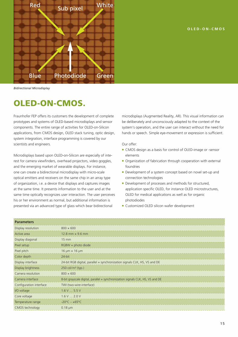
OLED-ON-CMOS.Fraunhofer FEP offers its customers the development of complete
prototypes and systems of OLED-based microdisplays and sensor
components. The entire range of activities for OLED-on-Silicon
applications, from CMOS design, OLED stack tuning, optic design,
system integration, interface programming is covered by our
scientists and engineers.
Microdisplays based upon OLED-on-Silicon are especially of inte-
rest for camera viewfinders, overhead projectors, video goggles,
and the emerging market of wearable displays. For instance,
one can create a bidirectional microdisplay with micro-scale
optical emitters and receivers on the same chip in an array type
of organization, i.e. a device that displays and captures images
at the same time. It presents information to the user and at the
same time optically recognizes user interaction. The user perceives
his or her environment as normal, but additional information is
presented via an advanced type of glass which bear bidirectional
O L E D - O N - C M O S
microdisplays (Augmented Reality, AR). This visual information can
be deliberately and unconsciously adapted to the context of the
system‘s operation, and the user can interact without the need for
hands or speech. Simple eye-movement or expression is sufficient.
Our offer:
▪ CMOS design as a basis for control of OLED-image or -sensor
elements
▪ Organization of fabrication through cooperation with external
foundries
▪ Development of a system concept based on novel set-up and
connection technologies
▪ Development of processes and methods for structured,
application specific OLED, for instance OLED microstructures,
OLED for medical applications as well as for organic
photodiodes
▪ Customized OLED silicon wafer development
Parameters
Display resolution 800 × 600
Active area 12.8 mm × 9.6 mm
Display diagonal 15 mm
Pixel setup RGBW + photo diode
Pixel pitch 16 µm × 16 µm
Color depth 24-bit
Display interface 24-bit RGB digital, parallel + synchronization signals CLK, HS, VS and DE
Display brightness 250 cd / m² (typ.)
Camera resolution 800 × 600
Camera interface 8-bit grayscale digital, parallel + synchronization signals CLK, HS, VS and DE
Configuration interface TWI (two-wire-interface)
I/O voltage 1.6 V … 5.5 V
Core voltage 1.6 V … 2.0 V
Temperature range -20°C – +65°C
CMOS technology 0.18 µm
Sub pixel
Photodiode
Red White
Blue Green
Bidirectional Microdisplay
16
17
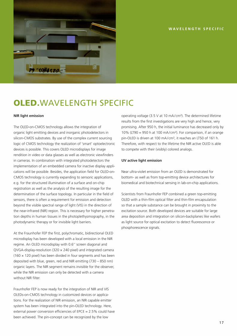
OLED.WAVELENGTH SPECIFICNIR light emission
The OLED-on-CMOS technology allows the integration of
organic light emitting devices and inorganic photodetectors in
silicon-CMOS substrates. By use of the complex current sourcing
logic of CMOS technology the realization of ‘smart’ optoelectronic
devices is possible. This covers OLED microdisplays for image
rendition in video or data glasses as well as electronic viewfinders
in cameras. In combination with integrated photodetectors the
implementation of an embedded camera for inactive display appli-
cations will be possible. Besides, the application field for OLED-on-
CMOS technology is currently expanding to sensoric applications,
e.g. for the structured illumination of a surface and on-chip
registration as well as the analysis of the resulting image for the
determination of the surface topology. In particular in the field of
sensors, there is often a requirement for emission and detection
beyond the visible spectral range of light (VIS) in the direction of
the near-infrared (NIR) region. This is necessary for higher penetra-
tion depths in human tissues in the photoplethysmography, in the
photodynamic therapy or for invisible light barriers.
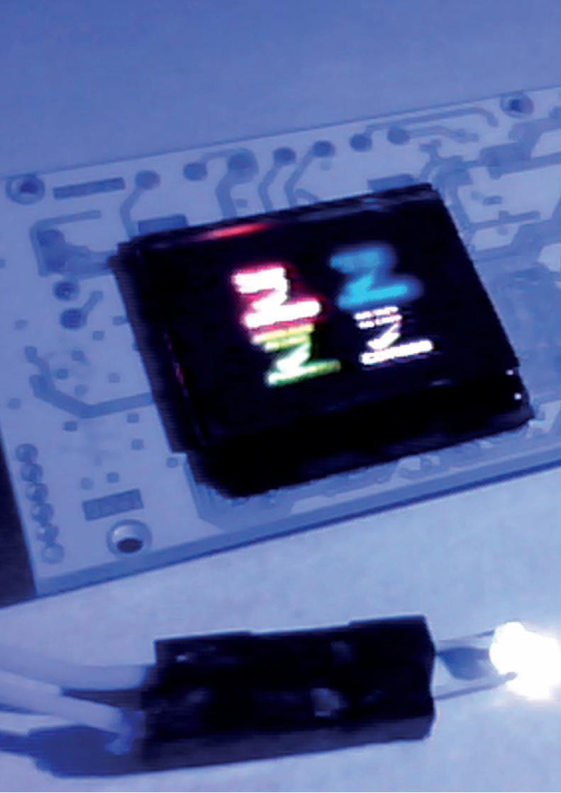
At the Fraunhofer FEP the first, polychromatic, bidirectional OLED
microdisplay has been developed with a local emission in the NIR
regime. An OLED microdisplay with 0.6’’ screen diagonal and
QVGA-display-resolution (320 × 240 pixel) and integrated camera
(160 × 120 pixel) has been divided in four segments and has been
deposited with blue, green, red and NIR emitting (730 – 850 nm)
organic layers. The NIR segment remains invisible for the observer,
while the NIR emission can only be detected with a camera
without NIR filter.
Fraunhofer FEP is now ready for the integration of NIR and VIS
OLEDs-on-CMOS technology in customized devices or applica-
tions. For the realization of NIR emission, an NIR capable emitter
system has been integrated into the pin-OLED technology. Here,
external power conversion efficiencies of EPCE = 2.5% could have
been achieved. The pin-concept can be recognized by the low
W A V E L E N G T H S P E C I F I C
operating voltage (3.5 V at 10 mA / cm²). The determined lifetime
results from the first investigations are very high and hence, very
promising. After 950 h, the initial luminance has decreased only by
10% (LT90 = 950 h at 100 mA / cm²). For comparison, if an orange
pin-OLED is driven at 100 mA / cm², it reaches an LT50 of 161 h.
Therefore, with respect to the lifetime the NIR active OLED is able
to compete with their (visibly) colored analogs.
UV active light emission
Near ultra-violet emission from an OLED is demonstrated for
bottom- as well as from top-emitting device architectures for
biomedical and biotechnical sensing in lab-on-chip applications.
Scientists from Fraunhofer FEP combined a green top-emitting
OLED with a thin-film optical filter and thin-film encapsulation
so that a sample substance can be brought in proximity to the
excitation source. Both developed devices are suitable for large
area deposition and integration on silicon-backplanes like wafers
as light source for optical excitation to detect fluorescence or
phosphorescence signals.
18Illustration produced by Frank Hahnewald using Fraunhofer FEP OLED
19
CONTACT.
Ines Schedwill
Phone +49 351 8823-238
Fax +49 351 8823-394
facebook.com/fraunhoferfep
www.fep.fraunhofer.de
youtube.com/fraunhoferfep
linkedin.com/company/fraunhofer-fep
xing.com/companies/fraunhoferfep
twitter.com/fraunhoferfep
L O C A T I O N W I N T E R B E R G S T R A S S E
C O N T A C T P E R S O N P I C T U R E C R E D I T S
L O C A T I O N M A R I A - R E I C H E - S T R A S S E
Fraunhofer Institute for
Organic Electronics, Electron Beam and Plasma Technology FEP
Winterbergstr. 28 | 01277 Dresden, Germany
Phone +49 351 2586-0
Fax +49 351 2586-105
www.fep.fraunhofer.de
Fraunhofer Institute for
Organic Electronics, Electron Beam and Plasma Technology FEP
Maria-Reiche-Str. 2 | 01109 Dresden, Germany
Phone +49 351 8823-238
Fax +49 351 8823-394
www.fep.fraunhofer.de
Some of the pictures in this brochure are copyright by:
Jürgen Lösel
André Wirsig
C O N T A C T

© F R A U N H O F E R F E P – 2 . 2 – L 1 0
We focus on quality
and the ISO 9001.