Embed Size (px)
Citation preview

Curriculum Vitae of D. K. Avasthi 1. Name :Dr. Devesh Kumar Avasthi 2. Academic Qualifications :Ph.D.(Physics) from Panjab University, Chandigarh in 1982. 3. Research Interest : Nanotechnology, Materials for energy, Ion beam Engineering of
Materials, Radiation damage, Plasmonics, Radiation Biology 4. Positions Held: 1980-81 & 81-82 Lecturer, DAV College, Chandigarh, while doing Ph.D. at PU, Chandigarh 1982-1986 Scientist 'B' Defence Research Development Laboratory, Hyderabad 1986-2015 at Inter University Accelerator Centre, Formerly known as ‘Nuclear
Science Centre’, New Delhi -110 067 (Scientist H from April 2006 to 31st December 2015) March 2016 onwards: Professor, Director, Amity Institute of Nanotechnology and Director, Directorate of Engineering and Technology, Amity University Noida
5. Positions Held:
1980-81& 81-82 Lecturer, DAV College, Chandigarh, while doing Ph.D. at PU, Chandigarh
1982-1986 Scientist 'B' Defence Research Development Laboratory, Hyderabad
1986-2015 at Inter University Accelerator Centre, Formerly known as ‘Nuclear Science
Centre’, New Delhi -110 067
(Scientist H since April 2006 to 31st December 2015)
March 2016 onwards: Professor, Amity Institute of Nanotechnology and
Director, Directorate of Engineering and Technology, Amity University Noida
6. Academic Vists Abroad
(a) Visit to Tsukuba University, Japan for three months, funded by by Deptt.of Science & Technology,
Govt.of India in 1991, under BOYSCAST fellowship.
(b) Visit to Tandem Accelerator Laboratory, Ludwig Maximilian university (LMU), Munich, Germany
funded by by Deutscher Akademisch Austachsdienst, Bonn for 3 months from 15th September
1996, under DAAD fellowship.
(c) Three weeks (i) visits to LMU Munich, Germany in 1998,1999 and 2001 for DST - BMBF project.
(d) Three weeks trip to Stuttgat univ./MPI Stuttgart, Germany for DST-DAAD project in 2003 & 2004.
(e) Two weeks visits to CSNSM Orsay, France in 1999, 2003, 2005 and 2006 for Indo French project by
IFCPAR. The project was graded excellent by the scientific advisory committee of IFCPAR.
(f) Visiting scientist to Kiel University, Germany in 2005 and 2008 for two months and one month
respectively.
(g) Visiting scientist at Padova university, Italy in 2007 & 2009 for 3 weeks and 2 weeks respectively.
(h) Visiting scientist at NIMS Tsukuba, Japan in May 2010 for three weeks, supported by NIMS Japan.
(i) Visit to Kiel university, Germany for one week to explore the area of Nano Bio research in 2011.
(j) Visit to European Synchrotron Radiation Facility (ESRF), Grenoble, France to perform experiments
at Synchrotron beam lines in 2008 for one week.
(k) Visit to Synchrotron laboratory Elettra Trieste, Italy to perform experiments at Synchrotron beam
lines for one week each in 2011, 2012, 2015 and 2016.
(l) Visit to KEK photonn factory Tsukuba, Japan for experiments in Synchrotron beamline for one week
each in 2012, 2014 and 2016.
(m) Visit to DESY Hamburg, Germany for experiments in Synchrotron beamline for one week each in
2012, 2013 and 2016.

(n) Three weeks research visit to NIMS Tsukuba, Japan in 2012 for DST-JSPS project.
(o) Two weeks visit St. Petersburg, Russia under a collaborative research program in 2014 alongwith
visit to JINR Dubna and Institute of crystallography, Moscow for seminars.
(p) Visit to Caen, France from 10th to 14th May 2015, as a Coordinator of Indo French workshop on
'Interdisciplinary investigations of ion beam interactions with matter: From fundamental aspects to
nanotechnology and hadronbiology'. Subsequently participation in international conference 'Swift
Heavy Ion in Matter, SHIM' in Darmstadt, Germany and one week visit to LMU Munich in Laser
plasma acceleration-Medical physics group.
(q) Visit to LMU Munich for research discussions in June 2016.
7. Professional Recognition
(i) Fellow of Institue of Physics, UK.
(ii)Founder President of 'Ion Beam Society of India'.
(iii) Rajiv Gandhi Gold Medal award for research in 2016 by Global Economic Progress & Research
Association, (GEPRA), Tamil Nadu.
(iv) Got BOYSCAST fellow award for research in Tsukuba University, Japan for three months, Japan by
Deptt.of Science & Technology, Govt.of India in 1991.
(v) Reciepent of DAAD fellowship for research at Tandem Accelerator Laboratory, Munich by Deutscher
Akademisch Austachsdienst, Bonn for 3 months from 15th September 1996.
(vi) Yuva Shakti Puraskar in Science by Akhil Bhartiya Vidyarthi Parishad, ABVP, in 1985.
(vii) Member of editorial board of Vacuum, an international journal published by Elsevier Science.
(viii) Associate editor of international journal 'Radiation Effects and Defects in Solids'.
(ix) Member of international scientific advisory committee of bi-annual international conference on
"Ion Beam Analysis" since 2001.
(x) Member of international scientific advisory committee of bi-annual international conference on
‘Modification of properties of surface layers of non semiconducting materials using particle beams’.
(xi) Member of International committee of international conference on ‘Swift Heavy Ion in Matter
(SHIM)’, since May 2005.
(xii) Member of international committee of International conference on ‘Radiation Efeects in Insulators’
since September 2009.
(xiii) Secretary of international conference on 'Swift Heavy Ions in Materials Engineering and
Characterization' held at India International Centre, New Delhi in october 1998.
(xiv) Convenor of ‘International conference on ion tracks in solids’, held at India Habitat Centre, New
Delhi, Oct 2002.
(xv) Convener of Indo German workshop on ‘Synthesis and modification of nanostructures by ion
beams’ held at ICGEB, Delhi in Feb. 2005.
(xvi) Co-chairman of the International conference on ‘Ion Beam Analysis’, IBA held at at ISB
Hyderabad, Sept. 2007.
(xvii) Co- chairman of the Indo French conference on ‘Nanostructuring by ion beams’ in Feb. 2009
held at Trident Hotel, Bhubaneswar.
(xviii) Chairman of international conference on 'Swift heavy ions in materials engineering and
characterization' in October 2010, IUAC Delhi.
(xix) Co-chairman of conference on ‘Nanostructuring by ion beams’ at Allahabad university, Oct. 2011.
(xx) Chairman of international school on 'Ion Beams in Materials Science' in October 2012, IUAC
Delhi.
(xxi) Chairman of international conference on 'Swift heavy Ions in Materials Engineering and
Characterization' held at ICGEB Delhi, in October 2012.
(xxii) Chairman of the international conference on 'Nanostructuring by Ion Beams' at Gold Palace
resort, Jaipur in October 2013.
(xxiii) Convener of, workshop on "Ecologically Sustainable Energy Sources for Rural Development" in
XXXVII Indian Social Science Congress, held in Dec. 27Th to 31st December 2013 in AMU Aligarh.
(xxiv) Chairman of International conference on 'Swift Heavy Ions in Materials Engineering and
Characterization', held in New Delhi in October 2014.
(xxv) Coordinator of Indo French workshop on 'Interdisciplinary investigations of ion beam
interactions with matter: From fundamental aspects to nanotechnology and hadronbiology', held in Caen,
France, 10th to 14th May 2015.
(xxvi) Chairman of 18th international conference on 'Radiation effects in Insulators', held in Jaipur
in Oct. 2015.
(xxvii) Chairman of international conference on 'Nanostructuring by ion beams', held in Agra in
Nov. 2015.
7. Research Experience: i. Research Interest: Main interest has been ion beams for analysis,
modification of materials, synthesis and engineering the nanostructures, Carbon nanostructures:
fullerene, CNT and graphene, surface and interface modification by ion beams, plasmonics, surface
enhanced Raman scattering, thermoelectric materials. Initiated activities in nanocomposite thin films
and interaction of metal nanoparticles with cancer cell for SERS and enhancement in
radiosensitization at IUAC. Recent work in this direction is cited in NATURE INDIA as a news
in one of the issues in April 2013. Nucleated research programs with national and international
collaborations in the field of electronic sputtering, ion beam mixing and ion beams based synthesis of
nanostructures. The major research projects are under ‘Intensifying Research in High Priority Area’
scheme and another under ‘Nano Mission’ funded by Department of Science and Technology. Details
of research programs based on collaborations and funded by Government bodies is given under the
heading projects undertaken. Have several international collaborations with research groups in Munich,
Stuttgart, Kiel, Orsay, Padova, Tsukuba, St. Petersburg and Taiwan, funded by DST and IFCPAR,
Delhi.
Highlights of research work are given in Annexe A.
ii. Ph.D. students: Supervised the research of twenty four students, who got Ph.D. degrees under my
supervision/co-supervision. Currently having six research scholars for Ph.D. Six former Ph.D. students are
now faculty at institutes of excellence like IIT Delhi, IIT Kharagpur, NIT Jaipur, Notre Dam university,
USA, Kiel university Germany. Two Ph.D. students got Humboldt fellowship award.
iii. Facility Development:
Had a key role in establishing a high vacuum laboratory to provide a support to accelerator and
a target development laboratory to provide targets/samples to the researchers from universities.
Two out of several papers related to above activities are:
S. Mandal, D. Kabiraj, D.K. Avasthi, “Preparation and characterization of a sandwiched target
of enriched neodymium oxide”, Nucl. Instr. and Meth. A 397 (1997) 59.
A. Tripathi, N. Singh, D.K. Avasthi, “Hydrogen intake capacity of ZrVFe alloy bulk getters”,
Vacuum 48 (1997) 1023.
Had a responsibility of design, fabrication and installation of a 1.5 meter diameter general
purpose scattering chamber (GPSC) with vacuum control system and detector arms control
system in beam line of the accelerator, which is being used in nuclear physics and materials
science experiments.
A RF sputtering set up was fabricated using a RF power amplifier developed by a colleague at
IUAC. The set up was used for making thin films for experiment with ion beams. One of the
most cited work using this facility is:
S. Ghosh, D.K. Avasthi, P. Shah, V. Ganesan, A. Gupta, D. Sarangi, R. Bhattacharya, W.
Assmann, “Deposition of thin films of different oxides of copper by RF reactive sputtering and
their characterization”, Vacuum 57 (2000) 377.
Designed and implemented an experimental set up for energy loss measurement.
It was published in
A. Bhagwat and D.K. Avasthi, “A new experimental arrangement for energy loss
measurements”, Japanese Journal of Applied Physics, Part 1: Regular Papers and Short Notes
and Review Papers 35 (1996) 313.
A low flux irradiation attachment to GPSC was designed and implanted for energy
straggling/loss measurement & test of space devices. One of research papers using this facility
is:
P.K. Gulati, Pratibha K. Gulati, Neetu Munjal, P. K. Diwan, V. Sharma, S. Kumar, S. A. Khan,
and D. K. Avasthi, Phys. Rev. A 80 (2009) 022512.
Implemented elastic recoil detection analysis (ERDA) technique for H depth profiling and light
lement depth profiling, using the experience of nuclear techniques. One of the papers in this
area is:
D.K. Avasthi, M.G. Acharya, R.D. Tarey, L.K. Malhotra, G.K.Mehta, “Hydrogen profiling and
the stoichiometry of an a-SiNx:H film”, Vacuum 46 (1995) 265.
Later a large area position sensitive telescope detector (LAPSTD) was designed, fabricated and
installed to enhance the capabilities of ERDA, which was used for electronic sputtering
measurements. On-line ERDA using LAPSDT was implemented in two beam lines.
Developmental work was reported in:
S.V.S. Nageswara Rao, A. Kothari, G.B.V.S. Lakshmi, S.A. Khan, A. Tripathi, A.M. Siddiqui,
A. P. Pathak, D.K. Avasthi, “Development of a large area two-dimensional position sensitive
ΔE-E detector telescope for material analysis”, Nucl. Instr. and Meth. B 212 (2003) 545.
The most recent developments has been an atom beam sputtering set up for synthesis of
nanocomposite thin films. The most cited research paper using this facility is:
D.K. Avasthi et al., 'Synthesis of metal polymer nanocomposite for optical applications',
Nanotechnology 18(2007)125604. [Cited 70 times]
An on-line QMA in accelerator beam line in beam hall I was installed in ultra high vacuum
chamber to understand the chemical reaction/modifications within ion track. One of the papers
is:
Jai Prakash, A. Tripathi, S. A. Khan, J. C. Pivin, F. Singh, Jalaj Tripathi, Sarvesh Kumar, and
D. K. Avasthi, Ion beam induced interface mixing of Ni on PTFE bilayer system studied by
quadrupole mass analysis and electron spectroscopy for chemical analysis, Vacuum 84(11)
(2010) 1275-12
79.
In-situ XRD was designed and installed in beam line in beam hall II to study ion beam
irradiation induced phase transformation. Details of the facility are in:
P. K. Kulriya, F. Singh, A. Tripathi, R. Ahuja, A. Kothari, R. N. Dutta, Y. K. Mishra, Amit
Kumar and D. K. Avasthi, “Setup for in situ x-ray diffraction study of swift heavy ion
irradiated materials”, Rev. Sci. Instrum. 78, (2007) 113901
This is further augmented by the attachment of close cycle refrigerator to perform the
irradiation down to 20K and performing XRD in those conditions. Especially, in-situ XRD with
low temperature attachment is unique set up in the heavy ion accelerator beam line, not
existing anywhere in world.
A facility for irradiation at 1000K is installed and tested recently, of interest for nuclear
materials. The technical development and test results are published in:
P.K. Kulriya, Renu Kumari, Rajesh Kumar, V. Grover, R. Shukla, A.K. Tyagi, D.K. Avasthi,
'In-situ high temperature irradiation setup for temperature dependent structural studies of
materials under swift heavy ion irradiation' , Nucl. Instrum. And Meth. B 372(2014) 98.
Most of the above developments of facilities were funded by DST, DRDO and DAE-BRNS.
iv. Technology transfer
Member of team on DST project on RF power supply development for RF sputtering set
up.; It resulted in technology transfer of RF power supply to two companies namely (i)
Hind High Vacuum, Bangalore ands (ii) Vacuum Equipment Company, New Delhi
8. Publications:
(i) Papers in Journals - 540
(ii) Papers in International Conferences - 110
(iii) Papers in National Conference/Symp. - 160
(iv) Total citations of papers: ~ 8595.
(v) H factor: (from Google scholar) 40 as in Jan. 2017.
Top fifty cited research papers are given in Annexe B.
Research papers selected for Virtual journal of Science and Technology in Annexe C.
Invited talks/seminars/lectures are given in Annexe D.
Technical Reports: Annexe E.
8.1 Author of book and book chapter (i) Co-author of book on ‘Swift Heavy Ions for Materials Engineering and Nanostructuring’ published by
Capital, New Delhi and Springer, Germany 2011: Authors; D.K. Avasthi and G.K. Mehta.
(ii) Author of a chapter;’ Energetic Ion beams in nanostructuring: An overview’ in book titled ‘Synthesis and
engineering of nanostructures by energetic ion beams’ by Nova publishers, USA, 2011.
(iii) Co-author of a chapter ‘Synthesis of metal nanocomposite thin films by atom beam co-sputtering’ in book
titled .‘Synthesis and engineering of nanostructures by energetic ion beams’ by Nova publishers, USA,
2011.
(iv) Co-author of a chapter 'Studies on ion irradiation induced modification of optical properties of Ag-C60, Ag-
C70 and Ag-a-C nanocomposite thin films', in book titled ‘Synthesis and engineering of nanostructures by
energetic ion beams’ by Nova publishers, USA, 2011.
(v) Co-author of a Chapter titled ‘ERDA: A tool for surface characterization’ in a book titled ‘Ion Beam
Analysis of Surfaces and Interfaces of Condensed Matter System’, Edited by P. Chakraborty, Nova Science
Publishers, USA, 2003.
(vi) Author of a chapter titled ‘Introduction to vacuum techniques and basic concepts’ in book titled ‘Ultra high
vacuum’ published by Allied publishers, Delhi, 2002.
(vii) Author of a chapter titled ‘Basic concepts for designing a vacuum system’, in book titled ‘Ultra high
vacuum’ published by Allied publishers, Delhi, 2002.
(viii) Co-author of a chapter titled 'Development of Getter pumps at NSC', in book titled ‘Ultra high vacuum’
published by Allied publishers, Delhi, 2002.
(ix) Co-author of a chapter titled 'Designing fabrication installation and commissioning of a cryo pump based
evaporator' in book titled ‘Ultra high vacuum’ published by Allied publishers, Delhi, 2002.
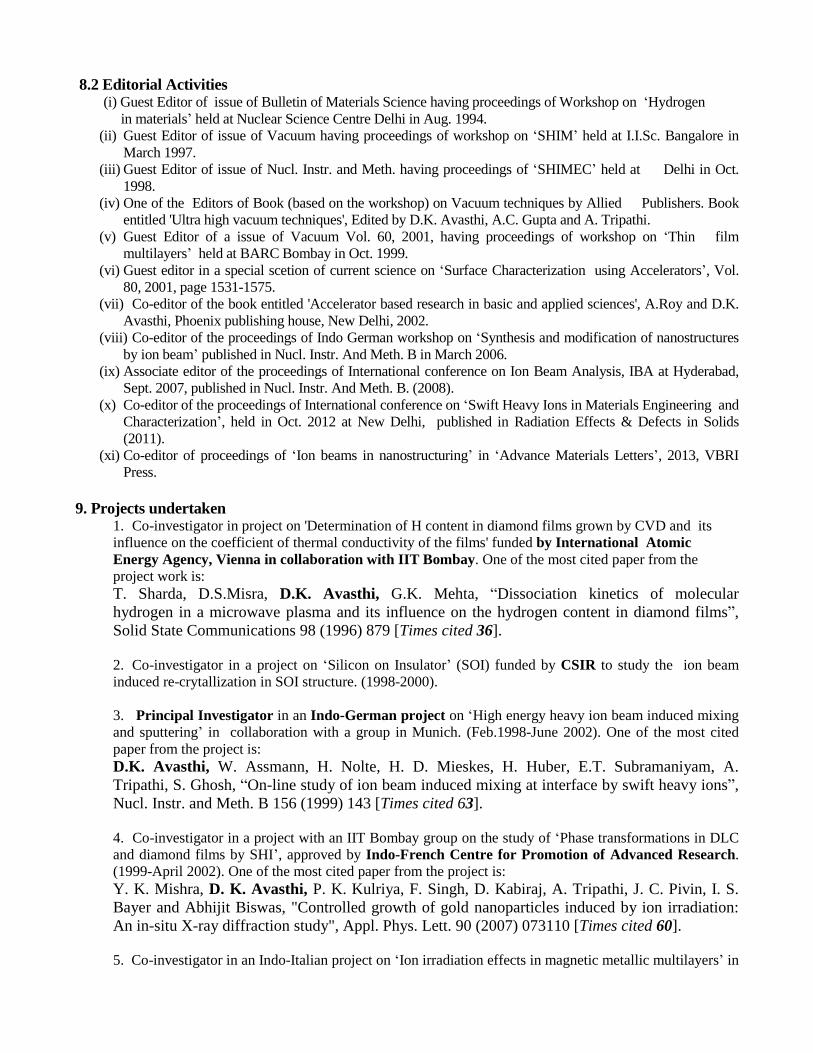
8.2 Editorial Activities (i) Guest Editor of issue of Bulletin of Materials Science having proceedings of Workshop on ‘Hydrogen
in materials’ held at Nuclear Science Centre Delhi in Aug. 1994.
(ii) Guest Editor of issue of Vacuum having proceedings of workshop on ‘SHIM’ held at I.I.Sc. Bangalore in
March 1997.
(iii) Guest Editor of issue of Nucl. Instr. and Meth. having proceedings of ‘SHIMEC’ held at Delhi in Oct.
1998.
(iv) One of the Editors of Book (based on the workshop) on Vacuum techniques by Allied Publishers. Book
entitled 'Ultra high vacuum techniques', Edited by D.K. Avasthi, A.C. Gupta and A. Tripathi.
(v) Guest Editor of a issue of Vacuum Vol. 60, 2001, having proceedings of workshop on ‘Thin film
multilayers’ held at BARC Bombay in Oct. 1999.
(vi) Guest editor in a special scetion of current science on ‘Surface Characterization using Accelerators’, Vol.
80, 2001, page 1531-1575.
(vii) Co-editor of the book entitled 'Accelerator based research in basic and applied sciences', A.Roy and D.K.
Avasthi, Phoenix publishing house, New Delhi, 2002.
(viii) Co-editor of the proceedings of Indo German workshop on ‘Synthesis and modification of nanostructures
by ion beam’ published in Nucl. Instr. And Meth. B in March 2006.
(ix) Associate editor of the proceedings of International conference on Ion Beam Analysis, IBA at Hyderabad,
Sept. 2007, published in Nucl. Instr. And Meth. B. (2008).
(x) Co-editor of the proceedings of International conference on ‘Swift Heavy Ions in Materials Engineering and
Characterization’, held in Oct. 2012 at New Delhi, published in Radiation Effects & Defects in Solids
(2011).
(xi) Co-editor of proceedings of ‘Ion beams in nanostructuring’ in ‘Advance Materials Letters’, 2013, VBRI
Press.
9. Projects undertaken 1. Co-investigator in project on 'Determination of H content in diamond films grown by CVD and its
influence on the coefficient of thermal conductivity of the films' funded by International Atomic
Energy Agency, Vienna in collaboration with IIT Bombay. One of the most cited paper from the
project work is:
T. Sharda, D.S.Misra, D.K. Avasthi, G.K. Mehta, “Dissociation kinetics of molecular
hydrogen in a microwave plasma and its influence on the hydrogen content in diamond films”,
Solid State Communications 98 (1996) 879 [Times cited 36].
2. Co-investigator in a project on ‘Silicon on Insulator’ (SOI) funded by CSIR to study the ion beam
induced re-crytallization in SOI structure. (1998-2000).
3. Principal Investigator in an Indo-German project on ‘High energy heavy ion beam induced mixing
and sputtering’ in collaboration with a group in Munich. (Feb.1998-June 2002). One of the most cited
paper from the project is:
D.K. Avasthi, W. Assmann, H. Nolte, H. D. Mieskes, H. Huber, E.T. Subramaniyam, A.
Tripathi, S. Ghosh, “On-line study of ion beam induced mixing at interface by swift heavy ions”,
Nucl. Instr. and Meth. B 156 (1999) 143 [Times cited 63].
4. Co-investigator in a project with an IIT Bombay group on the study of ‘Phase transformations in DLC
and diamond films by SHI’, approved by Indo-French Centre for Promotion of Advanced Research.
(1999-April 2002). One of the most cited paper from the project is:
Y. K. Mishra, D. K. Avasthi, P. K. Kulriya, F. Singh, D. Kabiraj, A. Tripathi, J. C. Pivin, I. S.
Bayer and Abhijit Biswas, "Controlled growth of gold nanoparticles induced by ion irradiation:
An in-situ X-ray diffraction study", Appl. Phys. Lett. 90 (2007) 073110 [Times cited 60].
5. Co-investigator in an Indo-Italian project on ‘Ion irradiation effects in magnetic metallic multilayers’ in

collaboration with IUC Indore and Padova University, Italy. (1998-2001). One of the most cited papers
is:
A. Gupta, A. Paul, R. Gupta, D.K. Avasthi, G. Principi, “The effect of swift heavy ion
irradiation on perpendicular magnetic anisotropy in Fe-Tb multilayers”, J. Phys.: Cond. Mat. 10
(1998) 9669. [Times cited 33].
6. Co-ordinator in a project on‘Ion beam mixing‘ in collaboration with NPL, funded by DST. (2000-
2003). One of the papers from project is:
K. Diva, D. Kabiraj, B.R. Chakraborty, S.M. Shivaprasad, D.K. Avasthi,
Investigation of V/Si mixing induced by swift heavy ions, Nucl. Instr. and Meth. B 222 (2004)
169 [Times cited 22].
7. Co-investigator an Indo-German project on ‘Ion beam mixing’ jointly with RBS college Agra, Stuttgart
university and MPI Stuttgart (2001-2003). One of the papers from the project is:
S. Kumar, R.S. Chauhan, S.A. Khan, W. Bolse, D.K. Avasthi, “Swift heavy ion induced mixing
in metal/metal system”, Nucl. Instr. And Meth. B244 (2006) 194. [Times cited 17].
8. Principal investigator of IRHPA project of DST entitled 'Swift heavy ion in materials engineering and
characterization' (2003-2006). Experimental facilities (ERDA and QMA) and AFM/STM were installed in
beam line under the project. One of the paper on development of a special detector is:
S. A. Khan, M. Kumar and D. K. Avasthi, “Development of a position sensitive detector
telescope for ERDA based on-line monitoring of swift heavy ions induced modifications”, Nucl.
Instr. & Meth. Phys. Res. B 266 (2008) 1912]. [Times cited 10]
9. Principal investigator in Indo French project on ‘Generation of nano phases by ion beams’, commenced
from 2003-2006. Graded excellent by scientific advisory committee of IFCPAR. One of the most cited
research papers from the project is:
J.C. Pivin, G. Roger, M.A. Garcia, F. Singh, D.K. Avasthi, “Nucleation and growth of Ag
clusters in silicate glasses under ion irradiation”, Nucl. Instr. and Meth. B 215 (2004) 373.
[Times cited 36].
10. Principal investigator in Joint research project between IUAC Delhi and Kiel University Germany,
on ‘Metal polymer nanocomposite and ion irradiation effects’ under DST-DFG with group of Prof. F.
Faupel, ended in Nov. 2007. One of the papers from the project is:
Y.K. Mishra, V.S.K. Chakravadhanula, U. Schrmann, Hardeep Kumar, D. Kabiraj, S. Ghosh, V.
Zaporojtchenko, D.K. Avasthi and F. Faupel, “Controlled reduction of size of Ag nanoparticles
embedded in teflon matrix by MeV ion irradiation”, Nucl. Instr. & Meth. Phys. Res. B 266
(2008) 1804]. [Times cited 10].
11. Co-investigator in DST project titled ‘Swift heavy ions induced nanostructure formation of thin oxide
films’, Dec. 2005 – Dec. 2008, with RBS College Agra. One of the papers from the project is:
D. C. Agarwal, R. S. Chauhan, D. K. Avasthi, S. A. Khan, D. Kabiraj and I. Sulania, “Formation
of self-affine nanostructures on ZnO surfaces by swift heavy ions”, J. Appl. Phys. 104 (2008)
024304. [Times cited 32].
12. Co-investigator of the project 'Activation of signalling molecules in human cells following heavy ion
irradiation and comparision with low LET radiation' from 2007 for 3 years with BARC, funded by DAE
BRNS Mumbai.
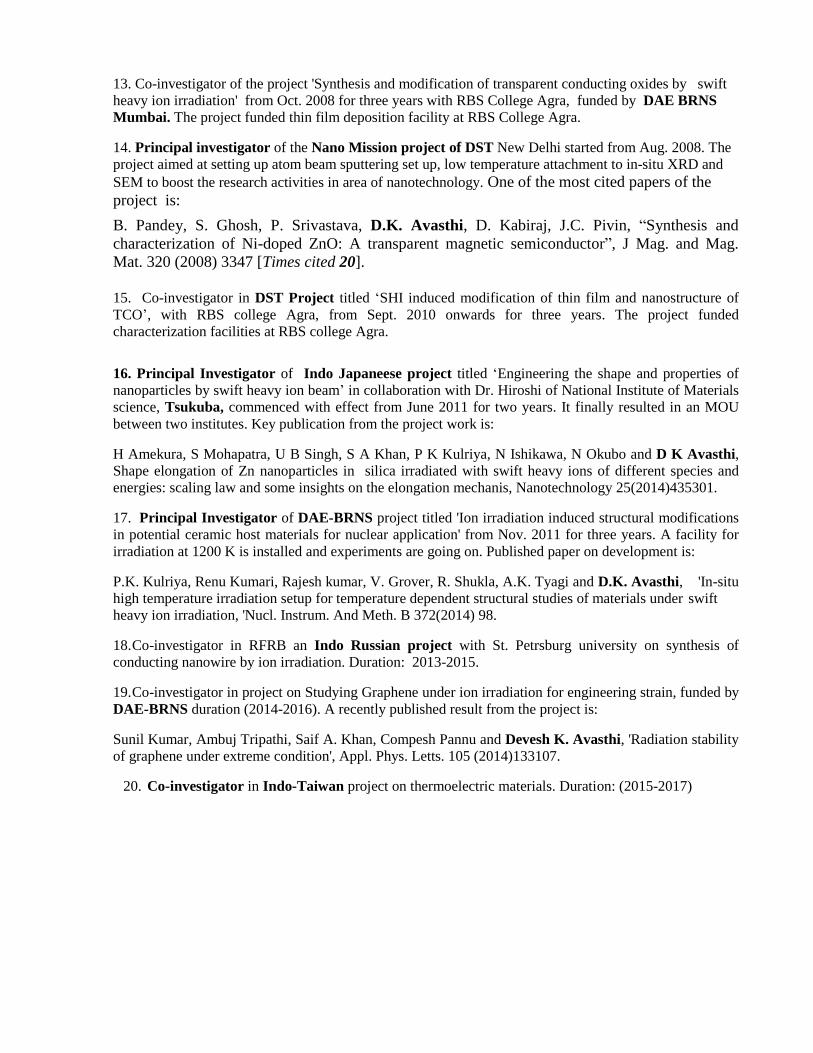
13. Co-investigator of the project 'Synthesis and modification of transparent conducting oxides by swift
heavy ion irradiation' from Oct. 2008 for three years with RBS College Agra, funded by DAE BRNS
Mumbai. The project funded thin film deposition facility at RBS College Agra.
14. Principal investigator of the Nano Mission project of DST New Delhi started from Aug. 2008. The
project aimed at setting up atom beam sputtering set up, low temperature attachment to in-situ XRD and
SEM to boost the research activities in area of nanotechnology. One of the most cited papers of the
project is:
B. Pandey, S. Ghosh, P. Srivastava, D.K. Avasthi, D. Kabiraj, J.C. Pivin, “Synthesis and
characterization of Ni-doped ZnO: A transparent magnetic semiconductor”, J Mag. and Mag.
Mat. 320 (2008) 3347 [Times cited 20].
15. Co-investigator in DST Project titled ‘SHI induced modification of thin film and nanostructure of
TCO’, with RBS college Agra, from Sept. 2010 onwards for three years. The project funded
characterization facilities at RBS college Agra.
16. Principal Investigator of Indo Japaneese project titled ‘Engineering the shape and properties of
nanoparticles by swift heavy ion beam’ in collaboration with Dr. Hiroshi of National Institute of Materials
science, Tsukuba, commenced with effect from June 2011 for two years. It finally resulted in an MOU
between two institutes. Key publication from the project work is:
H Amekura, S Mohapatra, U B Singh, S A Khan, P K Kulriya, N Ishikawa, N Okubo and D K Avasthi,
Shape elongation of Zn nanoparticles in silica irradiated with swift heavy ions of different species and
energies: scaling law and some insights on the elongation mechanis, Nanotechnology 25(2014)435301.
17. Principal Investigator of DAE-BRNS project titled 'Ion irradiation induced structural modifications
in potential ceramic host materials for nuclear application' from Nov. 2011 for three years. A facility for
irradiation at 1200 K is installed and experiments are going on. Published paper on development is:
P.K. Kulriya, Renu Kumari, Rajesh kumar, V. Grover, R. Shukla, A.K. Tyagi and D.K. Avasthi, 'In-situ
high temperature irradiation setup for temperature dependent structural studies of materials under swift
heavy ion irradiation, 'Nucl. Instrum. And Meth. B 372(2014) 98.
18. Co-investigator in RFRB an Indo Russian project with St. Petrsburg university on synthesis of
conducting nanowire by ion irradiation. Duration: 2013-2015.
19. Co-investigator in project on Studying Graphene under ion irradiation for engineering strain, funded by
DAE-BRNS duration (2014-2016). A recently published result from the project is:
Sunil Kumar, Ambuj Tripathi, Saif A. Khan, Compesh Pannu and Devesh K. Avasthi, 'Radiation stability
of graphene under extreme condition', Appl. Phys. Letts. 105 (2014)133107.
20. Co-investigator in Indo-Taiwan project on thermoelectric materials. Duration: (2015-2017)
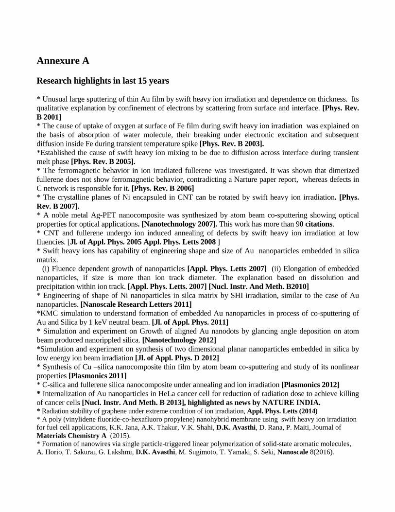
Annexure A
Research highlights in last 15 years
* Unusual large sputtering of thin Au film by swift heavy ion irradiation and dependence on thickness. Its
qualitative explanation by confinement of electrons by scattering from surface and interface. [Phys. Rev.
B 2001]
* The cause of uptake of oxygen at surface of Fe film during swift heavy ion irradiation was explained on
the basis of absorption of water molecule, their breaking under electronic excitation and subsequent
diffusion inside Fe during transient temperature spike [Phys. Rev. B 2003].
*Established the cause of swift heavy ion mixing to be due to diffusion across interface during transient
melt phase [Phys. Rev. B 2005].
* The ferromagnetic behavior in ion irradiated fullerene was investigated. It was shown that dimerized
fullerene does not show ferromagnetic behavior, contradicting a Narture paper report, whereas defects in
C network is responsible for it. [Phys. Rev. B 2006]
* The crystalline planes of Ni encapsuled in CNT can be rotated by swift heavy ion irradiation. [Phys.
Rev. B 2007].
* A noble metal Ag-PET nanocomposite was synthesized by atom beam co-sputtering showing optical
properties for optical applications. [Nanotechnology 2007]. This work has more than 90 citations.
* CNT and fullerene undergo ion induced annealing of defects by swift heavy ion irradiation at low
fluencies. [Jl. of Appl. Phys. 2005 Appl. Phys. Letts 2008 ]
* Swift heavy ions has capability of engineering shape and size of Au nanoparticles embedded in silica
matrix.
(i) Fluence dependent growth of nanoparticles [Appl. Phys. Letts 2007] (ii) Elongation of embedded
nanoparticles, if size is more than ion track diameter. The explanation based on dissolution and
precipitation within ion track. [Appl. Phys. Letts. 2007] [Nucl. Instr. And Meth. B2010]
* Engineering of shape of Ni nanoparticles in silca matrix by SHI irradiation, similar to the case of Au
nanoparticles. [Nanoscale Research Letters 2011]
*KMC simulation to understand formation of embedded Au nanoparticles in process of co-sputtering of
Au and Silica by 1 keV neutral beam. [Jl. of Appl. Phys. 2011]
* Simulation and experiment on Growth of aligned Au nanodots by glancing angle deposition on atom
beam produced nanorippled silica. [Nanotechnology 2012]
*Simulation and experiment on synthesis of two dimensional planar nanoparticles embedded in silica by
low energy ion beam irradiation [Jl. of Appl. Phys. D 2012]
* Synthesis of Cu –silica nanocomposite thin film by atom beam co-sputtering and study of its nonlinear
properties [Plasmonics 2011]
* C-silica and fullerene silica nanocomposite under annealing and ion irradiation [Plasmonics 2012]
* Internalization of Au nanoparticles in HeLa cancer cell for reduction of radiation dose to achieve killing
of cancer cells [Nucl. Instr. And Meth. B 2013], highlighted as news by NATURE INDIA. * Radiation stability of graphene under extreme condition of ion irradiation, Appl. Phys. Letts (2014)
* A poly (vinylidene fluoride-co-hexafluoro propylene) nanohybrid membrane using swift heavy ion irradiation
for fuel cell applications, K.K. Jana, A.K. Thakur, V.K. Shahi, D.K. Avasthi, D. Rana, P. Maiti, Journal of
Materials Chemistry A (2015).
* Formation of nanowires via single particle-triggered linear polymerization of solid-state aromatic molecules,
A. Horio, T. Sakurai, G. Lakshmi, D.K. Avasthi, M. Sugimoto, T. Yamaki, S. Seki, Nanoscale 8(2016).
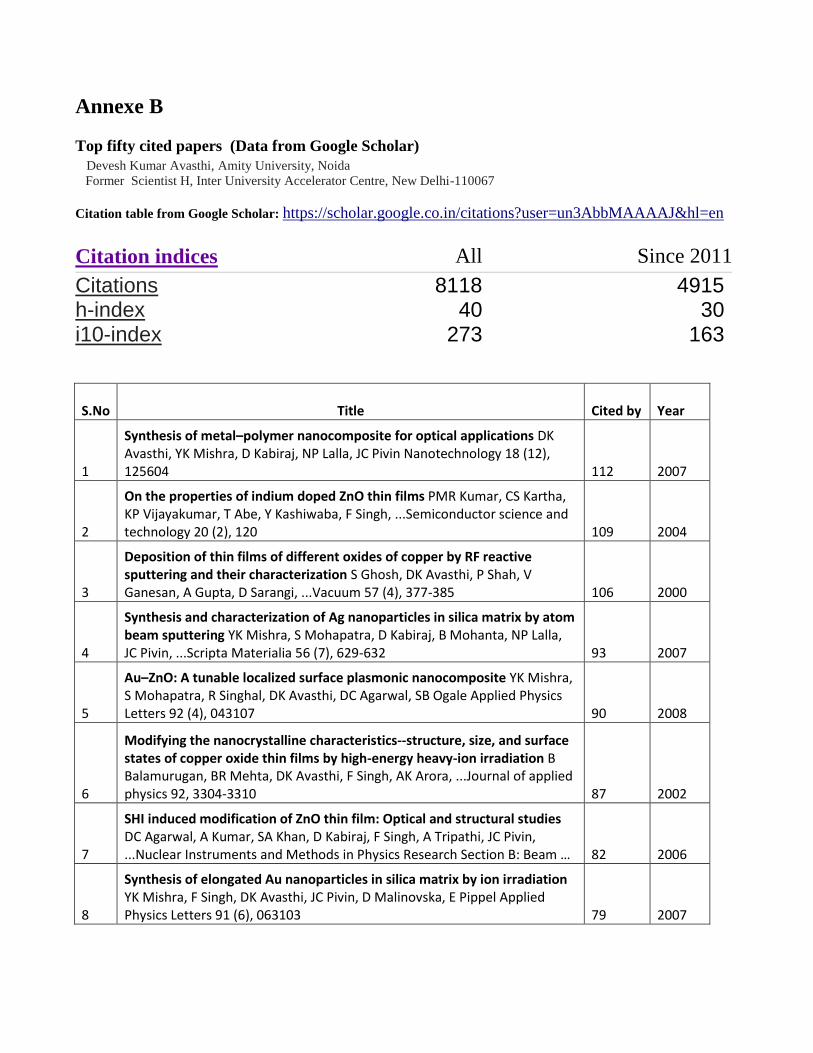
Annexe B
Top fifty cited papers (Data from Google Scholar)
Devesh Kumar Avasthi, Amity University, Noida
Former Scientist H, Inter University Accelerator Centre, New Delhi-110067
Citation table from Google Scholar: https://scholar.google.co.in/citations?user=un3AbbMAAAAJ&hl=en
Citation indices All Since 2011
Citations 8118 4915 h-index 40 30 i10-index 273 163
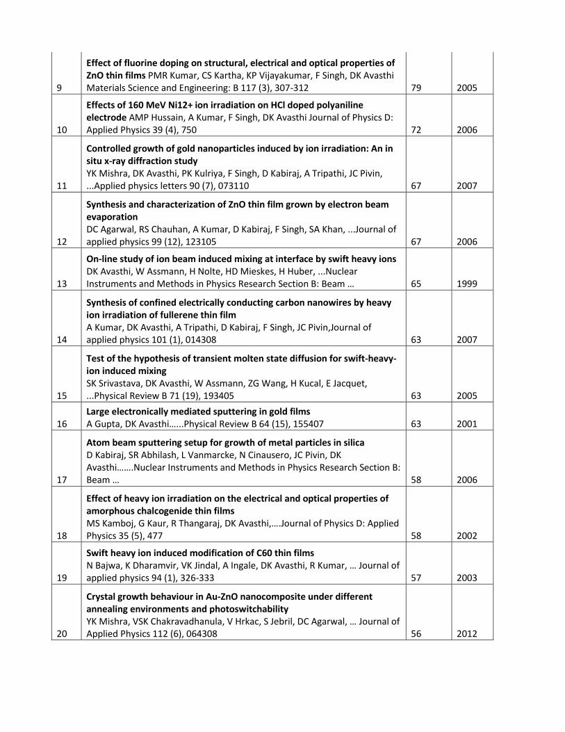
S.No Title Cited by Year
1
Synthesis of metal–polymer nanocomposite for optical applications DK Avasthi, YK Mishra, D Kabiraj, NP Lalla, JC Pivin Nanotechnology 18 (12), 125604 112 2007
2
On the properties of indium doped ZnO thin films PMR Kumar, CS Kartha, KP Vijayakumar, T Abe, Y Kashiwaba, F Singh, ...Semiconductor science and technology 20 (2), 120 109 2004
3
Deposition of thin films of different oxides of copper by RF reactive sputtering and their characterization S Ghosh, DK Avasthi, P Shah, V Ganesan, A Gupta, D Sarangi, ...Vacuum 57 (4), 377-385 106 2000
4
Synthesis and characterization of Ag nanoparticles in silica matrix by atom beam sputtering YK Mishra, S Mohapatra, D Kabiraj, B Mohanta, NP Lalla, JC Pivin, ...Scripta Materialia 56 (7), 629-632 93 2007
5
Au–ZnO: A tunable localized surface plasmonic nanocomposite YK Mishra, S Mohapatra, R Singhal, DK Avasthi, DC Agarwal, SB Ogale Applied Physics Letters 92 (4), 043107 90 2008
6
Modifying the nanocrystalline characteristics--structure, size, and surface states of copper oxide thin films by high-energy heavy-ion irradiation B Balamurugan, BR Mehta, DK Avasthi, F Singh, AK Arora, ...Journal of applied physics 92, 3304-3310 87 2002
7
SHI induced modification of ZnO thin film: Optical and structural studies DC Agarwal, A Kumar, SA Khan, D Kabiraj, F Singh, A Tripathi, JC Pivin, ...Nuclear Instruments and Methods in Physics Research Section B: Beam … 82 2006
8
Synthesis of elongated Au nanoparticles in silica matrix by ion irradiation YK Mishra, F Singh, DK Avasthi, JC Pivin, D Malinovska, E Pippel Applied Physics Letters 91 (6), 063103 79 2007
9
Effect of fluorine doping on structural, electrical and optical properties of ZnO thin films PMR Kumar, CS Kartha, KP Vijayakumar, F Singh, DK Avasthi Materials Science and Engineering: B 117 (3), 307-312 79 2005
10
Effects of 160 MeV Ni12+ ion irradiation on HCl doped polyaniline electrode AMP Hussain, A Kumar, F Singh, DK Avasthi Journal of Physics D: Applied Physics 39 (4), 750 72 2006
11
Controlled growth of gold nanoparticles induced by ion irradiation: An in situ x-ray diffraction study YK Mishra, DK Avasthi, PK Kulriya, F Singh, D Kabiraj, A Tripathi, JC Pivin, ...Applied physics letters 90 (7), 073110 67 2007
12
Synthesis and characterization of ZnO thin film grown by electron beam evaporation DC Agarwal, RS Chauhan, A Kumar, D Kabiraj, F Singh, SA Khan, ...Journal of applied physics 99 (12), 123105 67 2006
13
On-line study of ion beam induced mixing at interface by swift heavy ions DK Avasthi, W Assmann, H Nolte, HD Mieskes, H Huber, ...Nuclear Instruments and Methods in Physics Research Section B: Beam … 65 1999
14
Synthesis of confined electrically conducting carbon nanowires by heavy ion irradiation of fullerene thin film A Kumar, DK Avasthi, A Tripathi, D Kabiraj, F Singh, JC Pivin,Journal of applied physics 101 (1), 014308 63 2007
15
Test of the hypothesis of transient molten state diffusion for swift-heavy-ion induced mixing SK Srivastava, DK Avasthi, W Assmann, ZG Wang, H Kucal, E Jacquet, ...Physical Review B 71 (19), 193405 63 2005
16 Large electronically mediated sputtering in gold films A Gupta, DK Avasthi…...Physical Review B 64 (15), 155407 63 2001
17
Atom beam sputtering setup for growth of metal particles in silica D Kabiraj, SR Abhilash, L Vanmarcke, N Cinausero, JC Pivin, DK Avasthi…….Nuclear Instruments and Methods in Physics Research Section B: Beam … 58 2006
18
Effect of heavy ion irradiation on the electrical and optical properties of amorphous chalcogenide thin films MS Kamboj, G Kaur, R Thangaraj, DK Avasthi,….Journal of Physics D: Applied Physics 35 (5), 477 58 2002
19
Swift heavy ion induced modification of C60 thin films N Bajwa, K Dharamvir, VK Jindal, A Ingale, DK Avasthi, R Kumar, … Journal of applied physics 94 (1), 326-333 57 2003
20
Crystal growth behaviour in Au-ZnO nanocomposite under different annealing environments and photoswitchability YK Mishra, VSK Chakravadhanula, V Hrkac, S Jebril, DC Agarwal, … Journal of Applied Physics 112 (6), 064308 56 2012
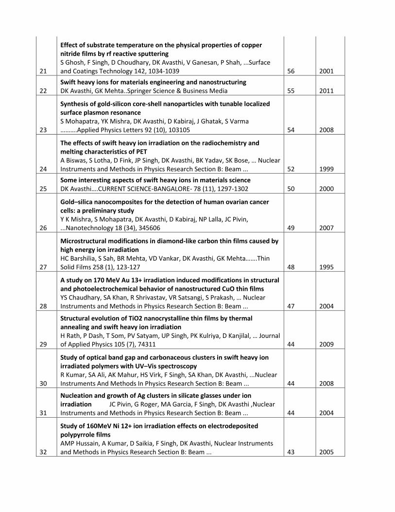
21
Effect of substrate temperature on the physical properties of copper nitride films by rf reactive sputtering S Ghosh, F Singh, D Choudhary, DK Avasthi, V Ganesan, P Shah, ...Surface and Coatings Technology 142, 1034-1039 56 2001
22 Swift heavy ions for materials engineering and nanostructuring DK Avasthi, GK Mehta..Springer Science & Business Media 55 2011
23
Synthesis of gold-silicon core-shell nanoparticles with tunable localized surface plasmon resonance S Mohapatra, YK Mishra, DK Avasthi, D Kabiraj, J Ghatak, S Varma ……….Applied Physics Letters 92 (10), 103105 54 2008
24
The effects of swift heavy ion irradiation on the radiochemistry and melting characteristics of PET A Biswas, S Lotha, D Fink, JP Singh, DK Avasthi, BK Yadav, SK Bose, … Nuclear Instruments and Methods in Physics Research Section B: Beam ... 52 1999
25 Some interesting aspects of swift heavy ions in materials science DK Avasthi….CURRENT SCIENCE-BANGALORE- 78 (11), 1297-1302 50 2000
26
Gold–silica nanocomposites for the detection of human ovarian cancer cells: a preliminary study Y K Mishra, S Mohapatra, DK Avasthi, D Kabiraj, NP Lalla, JC Pivin, ...Nanotechnology 18 (34), 345606 49 2007
27
Microstructural modifications in diamond-like carbon thin films caused by high energy ion irradiation HC Barshilia, S Sah, BR Mehta, VD Vankar, DK Avasthi, GK Mehta…….Thin Solid Films 258 (1), 123-127 48 1995
28
A study on 170 MeV Au 13+ irradiation induced modifications in structural and photoelectrochemical behavior of nanostructured CuO thin films YS Chaudhary, SA Khan, R Shrivastav, VR Satsangi, S Prakash, … Nuclear Instruments and Methods in Physics Research Section B: Beam ... 47 2004
29
Structural evolution of TiO2 nanocrystalline thin films by thermal annealing and swift heavy ion irradiation H Rath, P Dash, T Som, PV Satyam, UP Singh, PK Kulriya, D Kanjilal, … Journal of Applied Physics 105 (7), 74311 44 2009
30
Study of optical band gap and carbonaceous clusters in swift heavy ion irradiated polymers with UV–Vis spectroscopy R Kumar, SA Ali, AK Mahur, HS Virk, F Singh, SA Khan, DK Avasthi, ...Nuclear Instruments And Methods In Physics Research Section B: Beam ... 44 2008
31
Nucleation and growth of Ag clusters in silicate glasses under ion irradiation JC Pivin, G Roger, MA Garcia, F Singh, DK Avasthi ,Nuclear Instruments and Methods in Physics Research Section B: Beam ... 44 2004
32
Study of 160MeV Ni 12+ ion irradiation effects on electrodeposited polypyrrole films AMP Hussain, A Kumar, D Saikia, F Singh, DK Avasthi, Nuclear Instruments and Methods in Physics Research Section B: Beam ... 43 2005

33
Modifications of ZnO thin films under dense electronic excitation PMR Kumar, CS Kartha, KP Vijayakumar, F Singh, DK Avasthi, T Abe, … Journal of Applied Physics 97 (1), 013509 43 2005
34
Study on evolution of gases from Mylar under ion irradiation DK Avasthi, JP Singh, A Biswas, SK Bose Nuclear Instruments and Methods in Physics Research Section B: Beam ... 43 1998
35
Swift heavy ion induced formation of a-FeSi 2 W Assmann, M Dobler, DK Avasthi, S Kruijer, HD Mieskes, H Nolte,Nuclear Instruments and Methods in Physics Research Section B: Beam ... 42 1998
36
Synthesis and characterization of Ni-doped ZnO: a transparent magnetic semiconductor B Pandey, S Ghosh, P Srivastava, DK Avasthi, D Kabiraj, JC Pivin Journal of Magnetism and Magnetic Materials 320 (24), 3347-3351 41 2008
37
Ferromagnetism induced by heavy-ion irradiation in fullerene films A Kumar, DK Avasthi, JC Pivin, A Tripathi, F Singh Physical Review B 74 (15), 153409 41 2006
38
Ion tracks in silica for engineering the embedded nanoparticles DK Avasthi, YK Mishra, F Singh, JP Stoquert,Nuclear Instruments and Methods in Physics Research Section B: Beam ... 40 2010
39
Green luminescence of ZnS and ZnS: Cu quantum dots embedded in zeolite matrix SS Nath, D Chakdar, G Gope, J Kakati, B Kalita, A Talukdar, DK Avasthi,Journal of Applied Physics 105 (9), 094305 40 2009
40
Studies on the optical band gap and cluster size of the polyaniline thin films irradiated with swift heavy Si ions S Saravanan, MR Anantharaman, S Venkatachalam, DK Avasthi ,Vacuum 82 (1), 56-60 40
41
Swift heavy ion induced surface modification for tailoring coercivity in Fe–Ni based amorphous thin films S Thomas, H Thomas, DK Avasthi, A Tripathi, RV Ramanujan, ...Journal of Applied Physics 105 (3), 033910 39 2009
42
Transient enhanced diffusion of oxygen in Fe mediated by large electronic excitation DK Avasthi, W Assmann, A Tripathi, SK Srivastava, S Ghosh, F Grüner, ...Physical Review B 68 (15), 153106 39 2003
43
Recrystallization in polyvinylidene fluoride upon low fluence swift heavy ion impact A Biswas, R Gupta, N Kumar, DK Avasthi, JP Singh, S Lotha, D Fink, … Applied Physics Letters 78 (26) 39 2001
44 Hydrogen in chemical vapour deposited diamond films T Sharda, DS Misra, DK Avasthi Vacuum 47 (11), 1259-1264 39 1996
45
Study of hydrogen in DLC film by ERDA with 58 Ni ions DK Avasthi, D Kabiraj, GK Mehta, HC Barshilia, S Sah, BR Mehta, .. Vacuum 46 (7), 633-636. 38 1995
46
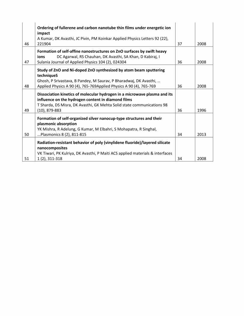
Ordering of fullerene and carbon nanotube thin films under energetic ion impact A Kumar, DK Avasthi, JC Pivin, PM Koinkar Applied Physics Letters 92 (22), 221904 37 2008
47
Formation of self-affine nanostructures on ZnO surfaces by swift heavy ions DC Agarwal, RS Chauhan, DK Avasthi, SA Khan, D Kabiraj, I Sulania Journal of Applied Physics 104 (2), 024304 36 2008
48
Study of ZnO and Ni-doped ZnO synthesized by atom beam sputtering techniqueS Ghosh, P Srivastava, B Pandey, M Saurav, P Bharadwaj, DK Avasthi, … Applied Physics A 90 (4), 765-769Applied Physics A 90 (4), 765-769 36 2008
49
Dissociation kinetics of molecular hydrogen in a microwave plasma and its influence on the hydrogen content in diamond films T Sharda, DS Misra, DK Avasthi, GK Mehta Solid state communications 98 (10), 879-883 36 1996
50
Formation of self-organized silver nanocup-type structures and their plasmonic absorption YK Mishra, R Adelung, G Kumar, M Elbahri, S Mohapatra, R Singhal, ...Plasmonics 8 (2), 811-815 34 2013
51
Radiation-resistant behavior of poly (vinylidene fluoride)/layered silicate nanocomposites VK Tiwari, PK Kulriya, DK Avasthi, P Maiti ACS applied materials & interfaces 1 (2), 311-318 34 2008
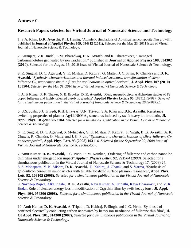
Annexe C
Research Papers selected for Virtual Journal of Nanoscale Science and Technology
1. S.A. Khan, D.K. Avasthi, K.H. Heinig, ‘Atomistic simulations of Au-silica nanocomposite film growth’,
published in Journal of Applied Physics 109, 094312 (2011), Selected for the May 23, 2011 issue of Virtual
Journal of Nanoscale Science & Technology.
2. Kiranjeet, V.K. Jindal, L.M. Bharadwaj, D.K. Avasthi and K. Dharamveer, "Damaged
carbonnanotubes get healed by ion irradiation," published in Journal of Applied Physics 108, 034302
(2010), Selected for the August 16, 2010 issue of Virtual Journal of Nanoscale Science & Technology.
3. R. Singhal, D. C. Agarwal, Y. K. Mishra, D. Kabiraj, G. Mattei, J. C. Pivin, R. Chandra and D. K.
Avasthi, “Synthesis, characterizations and thermal induced structural transformation of silver-
fullerene C60 nanocomposite thin films for applications in optical devices”, J. Appl. Phys.107 (2010)
103504. Selected for the May 31, 2010 issue of Virtual Journal of Nanoscale Science & Technology.
4. Amit Kumar, P. K. Thakur, N. B. Brookes, D. K. Avasthi, “X-ray magnetic circular dichroism studies of Fe
doped fullerene and highly oriented pyrolytic graphite" Applied Physics Letters 95, 182511 (2009). Selected
for a simultaneous publication in the Virtual Journal of Nanoscale Science & Technology 20 (2009) 21.
5. U.S. Joshi, S.J. Trivedi, K.H. Bhavsar, U.N. Trivedi, S.A. Khan and D.K. Avasthi, Resistance
switching properties of planner Ag/Li:NiO/ Ag structures induced by swift heavy ion irradiatio, Jl.
Appl. Phys. 105(2009)073704. Selected for a simultaneous publication in the Virtual Journal of Nanoscale
Science & Technology.
6. R. Singhal, D. C. Agarwal, S. Mohapatra, Y. K. Mishra, D. Kabiraj, F. Singh, D. K. Avasthi, A. K.
Chawla, R. Chandra, G. Mattei and J. C. Pivin, “Synthesis and characterizations of silver-fullerene C70
nanocomposite”, Appl. Phys. Lett. 93 (2008) 103114. Selected for the September 29, 2008 issue of
Virtual Journal of Nanoscale Science & Technology.
7. Amit Kumar, D. K. Avasthi, J. C. Pivin, P. M. Koinkar, ''Ordering of fullerene and carbon nanotube
thin films under energetic ion impact" Applied Physics Letter, 92, 221904 (2008). Selected for a
simultaneous publication in the Virtual Journal of Nanoscale Science & Technology 17, (2008) 24.
8. S. Mohapatra, Y. K. Mishra, D. K. Avasthi, D. Kabiraj, J. Ghatak, and S. Varma, ‘Synthesis of
gold-silicon core-shell nanoparticles with tunable localized surface plasmon resonance’, Appl. Phys.
Lett. 92, 103105 (2008), Selected for a simultaneous publication in the Virtual Journal of Nanoscale
Science & Technology.
9. Navdeep Bajwa, Alka Ingale, D. K. Avasthi, Ravi Kumar, A. Tripathi, Keya Dharamvir, and V. K.
Jindal, Role of electron energy loss in modification of C60 thin films by swift heavy ions , Jl. Appl.
Phys. 104, 054306 (2008), Selected for a simultaneous publication in the Virtual Journal of Nanoscale
Science & Technology
10. Amit Kumar, D. K. Avasthi, A. Tripathi, D. Kabiraj, F. Singh, and J. C. Pivin, ‘Synthesis of
confined electrically conducting carbon nanowires by heavy ion Irradiation of fullerene thin film’, Jl.
Of Appl. Phys. 101, 014308 (2007), Selected for a simultaneous publication in the Virtual Journal of
Nanoscale Science & Technology.
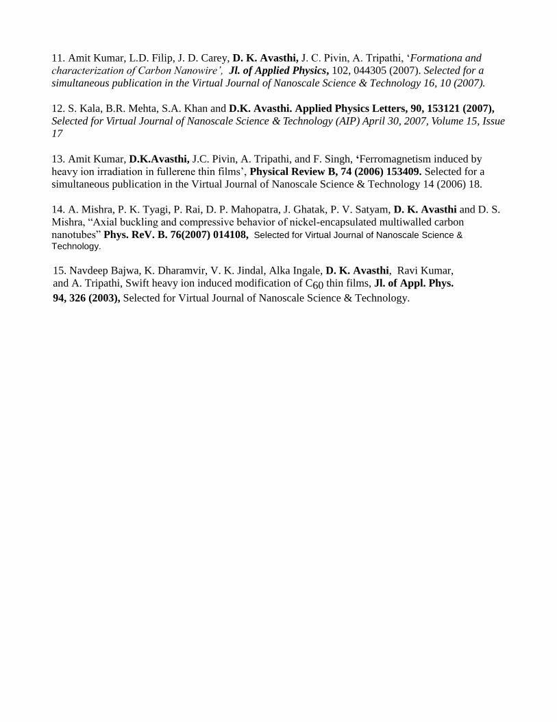
11. Amit Kumar, L.D. Filip, J. D. Carey, D. K. Avasthi, J. C. Pivin, A. Tripathi, ‘Formationa and
characterization of Carbon Nanowire’, Jl. of Applied Physics, 102, 044305 (2007). Selected for a
simultaneous publication in the Virtual Journal of Nanoscale Science & Technology 16, 10 (2007).
12. S. Kala, B.R. Mehta, S.A. Khan and D.K. Avasthi. Applied Physics Letters, 90, 153121 (2007),
Selected for Virtual Journal of Nanoscale Science & Technology (AIP) April 30, 2007, Volume 15, Issue
17
13. Amit Kumar, D.K.Avasthi, J.C. Pivin, A. Tripathi, and F. Singh, ‘Ferromagnetism induced by
heavy ion irradiation in fullerene thin films’, Physical Review B, 74 (2006) 153409. Selected for a
simultaneous publication in the Virtual Journal of Nanoscale Science & Technology 14 (2006) 18.
14. A. Mishra, P. K. Tyagi, P. Rai, D. P. Mahopatra, J. Ghatak, P. V. Satyam, D. K. Avasthi and D. S.
Mishra, “Axial buckling and compressive behavior of nickel-encapsulated multiwalled carbon
nanotubes” Phys. ReV. B. 76(2007) 014108, Selected for Virtual Journal of Nanoscale Science &
Technology.
15. Navdeep Bajwa, K. Dharamvir, V. K. Jindal, Alka Ingale, D. K. Avasthi, Ravi Kumar,
and A. Tripathi, Swift heavy ion induced modification of C60 thin films, Jl. of Appl. Phys.
94, 326 (2003), Selected for Virtual Journal of Nanoscale Science & Technology.
Annexe D
Invited talks/seminars/lectures in last ten years
2016
1. Seminar at IIT Karagpur on ‘Energetic Ions in Engineering Nanostructures’ on 12th Jan
2. Inaugural key note lecture in School/workshop on Accelerator Physics at Panjab University,
Chandigarh on 15th March 2016.
3. Seminar at HZDR Dresden, Germany on 2nd June 2016.
4. Lecture at IUAC Delhi in International School on Ion Beams in Materials Science on 23rd Sept.
5. Seminar at Hyderabad University on Ion Beams in Synthesis and Engineering of Nanostructures
on16th August.
6. Seminar on Accelerators in science and technology in VG University, Jaipur on 9th November.
2015 1. Inaugural address/talk on ' Ion beams in multi-discilplinary research' in 'National Conference on
Scientific Developments in 21st Century' at Jiwaji University, Gwalior, 12th March June.
2. Lecture on 'Synthesis and Engineering of nanostructures' in Ion beam school in Rajkot, 19th
March.
3. Lecture on ' Nano and ion beams to fight cancer' in Ion beam school in Rajkot, 20th March.
4. Invited talk on 'MeV ions in materials science' GGU, central university Bilaspur 30th March.
5. Invited talk on ‘Facilities and interesting aspects of ion beams in materials science’ at Indo French
conference at Caen on 13th May.
6. Invited talk on ‘Possible experiments in materials science with laser driven energetic ions’, in
international conference on ‘Applications of Laser driven Particle Acceleration’ in Venice on 21st
November.
7. Invited talk on ‘Engineering of nanostructures by ion beams’ in Solid state Physics symposium at
Amity university Noida on 21st Dec.
2014 1.Invited talk in International Conference on Nanoscience and Nanotechnology, Enhancement in
radiosensitization of cancer cells by Au nanoparticles, Panjab university, Chandigarh, Feb 13-15.
2. Inaugural talk:Ion beams in materials science A bird’s eye view, at CCCM Hyderabad: 20th
February.
3. Lecture in Students summer project programme of IUAC: Role of Ion Beams in Multi-disciplinary
Research: 18th June, IUAC Delhi.
4. Seminar title: Accelerator: Ideal laboratory for interdiscplinary research, science and technology,
S.S. Jain Subodh PG College, Jaipur, 2nd September
5. Invited talk in International conference on soft matter, : Ion beam based research in polymers at
IUAC, October 6, MNIT Jaipur
6. Lecture in SHIMEC school, Ion beams in materials of energy, October 10, IUAC Delhi
7. Seminar title 'Ion Beam Synthesis and Engineering of Nanostructures', 12th Nov., JINR Dubna
8. Seminar title Ion Beam Synthesis and Engineering of Nanostructures, 14th Nov., Institute of
Crystallography, Moscow
9.Seminar title 'Role of Ion Beam Synthesis and Engineering of Nanostructures',10th Dec, Kyushu
university, Japan
10.Seminar title 'In and around ion track: Disorder and order', 19th Dec, Osaka university, Japan
11.Invited talk in NCME-14, Role of Ion beams in materials of energy, SSJSPG College, Jaipur,
22nd Dec.
2013 1. Inaugural address and Invited talk in International Conference on Recent Innovations in Nano-
Bio-Polymer-Pharmaceutical Technologies, SETM university, Nanded, 13th jan.
2. Lecture series (5 lectures) in school on Ion Beams, organized by TIFR Mumbai, 18th to 20th Feb.
3. Lecture to school students on 28th Feb, IUAC, Delhi, (National Science day)
4. Invited talk on 'Energetic ions in materials for energy', in workshop on "Ecologically Sustainable
Energy Sources for Rural Development" in XXXVII Indian Social Science Congress, held in Dec. 27Th to
31st December 2013 in AMU Aligarh.
2012
1. Seminar on 'Research activity in nano & bio with ion beams;, 28th Sept, Tokyo Univ.
2. Invited talk on 'Exciting research opportunity in nanostructuring & nano bio with ion beams', 2nd
November, Seminar under DRS program, MSU Baroda.
3. Lecture to students: 'Ion matter interaction', Rajkot university, 5th Nov.
4. Invited Talk at Delhi university, Delhi on 'Role of ion beams in materials for energy', Indo-
German Workshop on Adv. Mat. for Future Energy Requirements, 29th Nov.
5. Invited talk at 'Research activity on gold nano particle for radiosensitivity in cancer cells', 27th Dec,
International conference on Nano-Pico technologyAmity University.
2011 1. Seminar ‘Synthesis of nanostructures by ion beams and possible applications’ Mumbai university,
14th June.
Invited talk ‘Facilities and research activities in nano and bio with ion beams at IUAC Delhi’, Indo
Singapore Joint Physics Symposium,Singapore, Feb. 24,.
3. Invited talk on 'Synthesisis of plasmonic nanostructures and possible applications', 22nd July, Brain
storming meeting NPL Delhi
4. Seminar on 'Research opportunities of research in materials science and radiation biology at IUAC',
21st April, Allahabad university
5. Seminar on 'Synthesis and engineering of nanostructures by ion beams, Jaipur university, DSA
program, 28th March
6. Invited talk on Nanostructuring by ion beams, NSMAT Banasthali university, 27th March
7. Seminar on 'Role of accelerator in science and technology', 24thoct., Dayal Singh College, Delhi
2010 1. 'Seminar on 'Synthesis and engineering of noble metal based nanocomposite thin film',
International conference on nanomaterials, Kottayam, April.
2. Seminar on 'Synthesis and engineering of nanostructures by ion beams': NIMS Tsukuba, Japan,
20th May.
3. Invited talk on 'Synthesis of nanostructures by ion beams', ICNST conference, IP University, 16th
November.
4. Ion Beams in Biomaterials: An Overview: IUAC Delhi, Biomaterials workshop, August.
5. Seminar on 'Ion beam facilities and research: Opportunities in materials science at IUAC Delh'i, 9th
August, BBA University Lucknow.
6. Seminar on 'Research activities in materials science with energetic ion's: Lucknow university:
10th August.
7. Seminar on 'Research activities in materials science with energetic ions': Dayalbagh Engineering
Institute, Agra, 18th September.
8. Lecture on 'Role of ion accelerators in science and technology', INSPIRE program at Amity
University, 17th November.
9. Lecture on 'Role of ion accelerators in science and technology', :INSPIRE program at Jaipur
university, 27th December 2010.
2009 1. Seminar on 'Nanostructures by ion beams, Delhi university: April
2. Invited talk on 'Ion tracks in silica for engineering the embedded nanoparticles' at International
conference REI, Padova Italy, Sept.
3. Seminar on 'Synthesis and engineering of nanostructures by energetic ions', 18th June, GSI,
Darmstadt
4. Seminar on 'Engineering and synthesis of nanostructures by ion beams': RRI Bangalore, 30th
5. Seminar on 'Research activities in mats. Sc. At IUAC', Stuttgart univ., 15th June
6. Seminar on 'Nanocomposite thin films and possible applications': Utkal university, March
7. Invited talk on 'Ion beam research in polymers:International conf. on polymer's, Goa, March
8. Invited talk on 'Nanostructuring by ion beams': Indo French conference, Bhubaneswar, Feb.
2008 1. Seminar on 'Energetic ion beams in materials science research activities at IUAC Delhi',
Singapore Light Source, NUS Singapore15th April
2. Seminar on 'Ion beam related polymer research at IUAC Delhi: Malaya University, Malaysia, 17th
April
3. Invited talk ‘Synthesis and characterization of metal nanocomposite for functional applications’:
International conference ANM at Aviero, Portugal, 23 June
4. Invited talk on 'ERDA for characterization and on-line experiments',:BARC Mumbai, 25th Sept.
5. Key note address in R symposium, IUMRS, 'Ion beam studies in CNT',Nagoya, Japan, Dec.
6. Seminar on 'Engineering and synthesis of nanostructures by ion beams', CUSAT Cochin, 5th June
7. Seminar on 'ERDA: Powerful tool for surface and interface analysis', 17th Jan. SSPL Delhi
8. Invited talk on 'Synthesis and engg. of nanostructures by ion beam', Pune university, 28th Jan
2007
1. Lecture on 'Nanostructuring by energetic ions', SSPL Delhi 23rd Aug.
2. Lecture on 'ERDA: Powerful tool for surface and interface analysis', SSPL Delhi, 23rd Aug.
3. Seminar on 'Nanostructuring by ion beams', Anna university, 30th Aug.
4. Seminar on 'Nanostructuring by ion beams', Mysore University 3rd Sept.
5. Invited talk on 'Synthesis of metal insulator nanocomposite for functional applications', in
international conference SMIB , TIFR Mumbai, 5th Oct.
6. Invited talk on 'Ion tracks in polymers for applications in nanotechnology', POLY2007, 2nd Nov.
7. Seminar on 'SeEngineering and synthesis of nanopsrticles by ion beams: Tirunelveli, 4th Feb. 2008
2006 1. Invited talk on 'Nanostructuring by ion beams', ICTP Trieste, June
2. Invited talk on 'Nanostructuring by eneretic ions at IUAC, Birla Science Centre, Hyderabad, Aug.
3. Seminar on 'Energetic ions in nanostructuring', Hyderabad university, Aug.
4. Invited talk on 'Synthesis of metal nanoparticles by physical vapour deposition', Kurukshetra
Univ., Sept.
5. Invited talk on 'Interesting features of SHI in C allotropes', International conference on DLC at
Kolkata, 1st Dec
6. Lecture on 'Research activities and facilities in materials science at IUAC', Acquaintance
program, Coimbatore, October
7. Lecture to school students 'Aspects of Nanotechnology in Biotechnology', Mothers International
School
2005 1. Invited talk on 'SeResearch activities in materials science with SHI', VECC Kolkata meetring
24th Jan. 2. Invited talk on 'Existence of transient temperature spike', CCCM Hyderabad, 10th Feb. 3. Seminar on 'Research activities in materials science with SHI', Mangalore Univ.: March
4. Seminars on 'Current research activities in materials science at NSC', Bochum and Rossendorf,
Germany, 27th May and 3rd June
5. Seminars on 'Ion beams in nano-structuring', GSI Darmstadt and Leipzig, Germany, 26th June,
2nd June
6. Colloquium:on 'Nanostructuring by energetic ions' IOP Bhubaneswar, 27th Nov.
7. Invited talk on 'Nano structuring by ion beams: Indo-Belarus workshop, ARCI Hyderabad,
23rd Dec.
2004 1. Seminar on 'Existence of transient temperature spike', 10th March, Hyderabad university
2. Seminar on 'Current research activities in materials science at NSC', Paris Univ.: Sept.
3. Seminar on 'Ion beams in nano-structuring', Ecole Polytechnique, Paris: Sept.
4. Lecture on 'Research activities of materials science with energetic ions in India: IOP-NSC School,
Oct. at IOP Bhubaneswar.
5. Lecture on 'Detectors, signal processing and data acquisition, IOP-NSC School, Bhubaneswar,
Oct. 6. Tutorial talk on 'Nano-structuring by RF sputtering', Univ.of Pune; Nov.

Annexe E
Technical reports
1. Preliminary design report of Trishul missile autopilot, S.Roy and D.K.Avasthi, 1984, DRDL
Hyderabad.
2. Preliminary design report on Prithvi missile autopilot, N.V.Kadam and D.K.Avasthi, 1985, DRDL
Hyderabad.
3. Design of an autopilot of missile, D.K.Avasthi and N.V. Kadam, 1985 DRDL Hyderabad, 1985.
4. Development of all metal UHV Faraday cup, R.Mehta, S. Muralidhar, D.K.Avasthi,
SC/TR/RM/92/25.
5. Technical report on general purpose scattering chamber GPSC, D.K.Avasthi, A.Tripathi, D.Kabiraj,
S.Venkataramanan, S.K.Datta, NSC/TR/DKA/92/16.
6. Experimental facilities at light ion beam room (-30 degree beam line), L.Senapati, Atripathi,
S.Gargari, D.K.Avasthi, A.K.Sinha, T.Srinivasan, S.Menon, SC/TR/LS/92/21.
7. Development of Titanium sublimation pump, A.Tripathi, L.Senapati, S.Bhatnagar, D.K.Avasthi,
NC/TR/AT/93/41.
8. Lower arm angle offset measurement at GPSC, A.Bhagwat, S.Mandal, A.Sarma, A.Mandal ,
D.K.Avasthi, NSC/TR/AB/93/94.
9. Local angle read out of target ladder at GPSC, R.Ahuja, T.Madhsoodhanan, D.K.Avasthi
Twin detector assembly for energy loss measurements, A.Bhagwat, R.Ahuja, D.K.Avasthi,
NSC/TR/AB/93/37.
10. Parallel plate electrostatic deflector, M.J.Singh, D.O.Kataria, N.M.Madhawan, J.J.Das, A.Tripathi,
D.K.Avasthi, A.K.Sinha, NSC/TR/MIS/93/36.
11. Software for simulation of ERDA, E.T.Subramaniyam, D.Kabiraj, D.K.Avasthi,
NSC/TR/ETS/94/84.
12. High energy ion beam assisted deposition set up at materials science beam line, G.K.Choudhary,
D.K.Avasthi, NSC/TR/GKC/95/114.
13. Differential pumping sysrtem, NSC/TR/GKC/95/93.
14. Technical report on sorption pump, G.K.Choudhury, S.Rao, Atripathi, D.K.Avasthi,
NSC/TR/GKC/95/107.
15. Stainless steel phase detector for 15 UD Pelletron accelerator at NSC, S.Ghosh, R.Ahuja, S.Rao,
A.Sarkar, D.K.Avasthi, D.Kanjilal, A.Roy, R.K.Bhowmik, NSC/TR/SG/95/112.
16. Fabrication and testing of a detector telescope, D.Kabiraj, D.O.Kataria, R.Ahuja, D.K.Avasthi,
NSC/TR/DK/96/139.
17. Design fabrication and installation of cryo based evaporator, D.Kabiraj, S.S.K.Sonti, D.K.Avasthi,
Technical Report NSC/TR/DK/98-99/11.
18. Low flux irradiation set up at GPSC, G.K.Choudhary, D.K.Avasthi
19. Ion channeling facility at NSC, T.Som, A.Tripathi, R.N.Dutt, A.Kothari, D.Kanjilal and D.K.Avasthi,
NSC/TR/TS/2001-02/5
20. Design, installation and testing of LAPSDT, S.A. Khan, M. Kumar, D.K. Avasthi, (2006).
21. In-situ XRD facility in beam line, P. Kulriya, F. Singh, A. Tripathi, D.K. Avasthi, (2007).