Embed Size (px)
Citation preview
VLSI DESIGN1997, Vol. 5, No. 3, pp. 273-284Reprints available directly from the publisherPhotocopying permitted by license only
(C) 1997 OPA (Overseas Publishers Association) Amsterdam B.V.Published in The Netherlands under license by
Gordon and Breach Science Publishers SAPrinted in Malaysia
Current Testing of CMOS Combinational Circuits withSingle Floating Gate Defects
VICTOR H. CHAMPACa’* and JOAN FIGUERASb
alnstituto Nacional de Astroffsica, Optica y Electr6nica, Grupo de Diseao de CI, Apdo. Postal 51 y 216, 72000 Puebla, Pue., Mexico;bUniversitat Politdcnica de Catalunya, Departament d’Enginyeria Electr6nica, Diagonal 649, Planta 9, 08028 Barcelona, Spain
The behavior of basic CMOS combinational gates in the presence of a floating gate defect ischaracterized in order to investigate its detectability by IzzQ. The defect is modeled at thecircuit level by the poly-bulk and metal-poly capacitances, which determine the quiescentpower supply current consumption (IDo) of the defective circuit. The testing implicationson the type of defective gate are studied. Experimental measures have been made on basicCMOS combinational modules designed with intentional floating gate defects. A good agree-ment is observed between the simulation results and the experimental data. A conventionalATPG for stuck-at faults is used to obtain the required exciting vector to test the floating gatedefects by Izo Testing.
Keywords: Defect modeling, floating gate defect, opens, current testing, exciting vectors, test pattern
1. INTRODUCTION
The class of defects due to opens causing a singletransistor gate to float (Floating Gate Defect) [1] [2][3] [4] [5] are physical failures that are not ade-quately represented by the stuck-at model. An open inthe conductive path to the gate can be produced bycontamination during manufacturing (spot defects)[6]. In addition, opens can also be produced by mi-crocracks at the step oxide. In this work large breaksare studied so that tunneling effects (studied by Hend-erson et al. [7]) in the breaks can be considered neg-ligible.The floating gate defect has sometimes been mod-
eled by the stuck-open model [8], assuming that thedefective transistor does not conduct. However, re-
cent research results [1] [2] [3] [4] [5] [9] show thatthe floating gate transistor may conduct in a wide
range of defect topologies. It has been shown that thebehavior of a floating gate transistor is influenced byseveral factors. The floating gate gets a voltage thatdepends on the coupling capacitances of the transistordevice and the surrounding circuitry [1] [2] [3] [4] [5][9]. In this work, the floating gate defect will be char-acterized at the circuit level taking into account thetechnology and topology of the circuit, and the phys-ical location of the break. Our objective is to investi-
gate the detectability of the floating gate defects byCurrent Testing [10] [11] [12]. Free-defective CMOSstatic circuits present a high impedance path betweenthe power supply and ground in its quiescent state.
*Corresponding author. Fax: 52-22-470517. E-mail: [email protected]
273
274 V.H. CHAMPAC and J. FIGUERAS
Consequently, the quiescent power supply currentconsumption (IDzQ) is very low. A current path be-tween VDo and Gvo in the quiescent state, establishedby an input exciting vector, may exist if a floatinggate transistor conducts when it should be "OFF"during a fault-free operation. The increase in the IozQcan be used to detect the defect. The influences of thegate topology (i.e. inverter, Nand, Nor) on the IDDadetectability is investigated. The most relevant as-
pects affecting the Izz are determined.In the next section, the electrical model of the
floating gate transistor with its coupling capacitancesis presented. The parameters influencing the degreeof conduction of the defective transistor are identi-fied. Next, the behavior of a simple inverter chainwith a floating gate defect is examined. The quiescentpower supply current consumption is characterized interms of the defect parameters. The analysis is ex-tended to basic CMOS combinational modules to
study the dependence of the gate structure on the
Io detectability. Basic CMOS combinational gateswith intentional floating gate defects have been builtand their IoD measured with the HP4145B Semicon-ductor Parameter Analyzer to compare with the pre-dicted Ioo levels using our modeling technique. Amethod to generate the exciting vectors to test thefloating gate defects by Current Testing, using a stan-dard ATPG for stuck-at faults, is proposed. Finally,the conclusions of the work are presented.
2. FLOATING GATE DEFECT MODEL
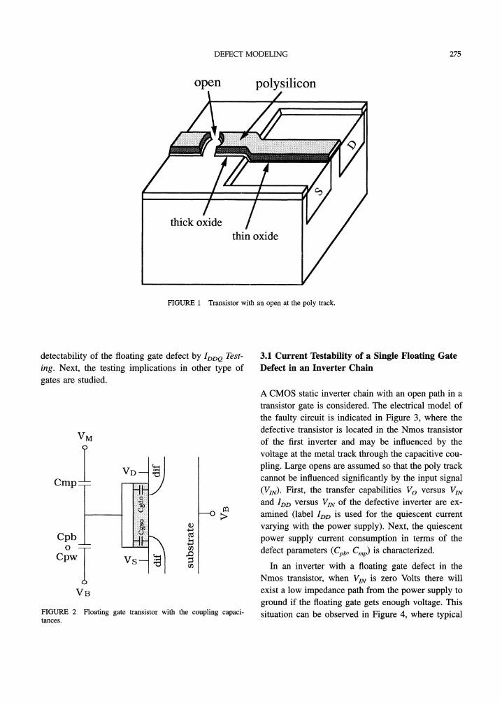
In this work, large opens in the transistor gate con-ducting path are considered. The poly path is brokenand the electrical connectivity to the gate is lost (SeeFigure 1). It has been shown that the behavior of afloating gate transistor is rather complex because thefloting node will get a voltage that depends on thecoupling capacitances to the transistor gate and onthe structure of the transistor itself [1] [2] [3] [4] [5][9].The voltage induced at the floating gate depends
on several factors:
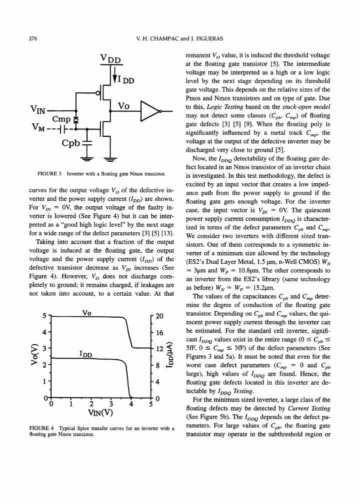
a) The location of the break failure influences thevalues of two capacitances:
The poly-bulk capacitance Cpb (poly-well capaci-tance for the Pmos transistors) that depends on thelength of the poly path that goes from the gate to
the location of the break (See Figure 1) as well ason the gate-substrate overlap capacitance (Cgbo).One terminal of these capacitances is connected to
the bulk voltage (Nmos), or else to the n-well volt-age (Pmos). For higher Cpb (Cpw) the degree ofconduction of an n-channel (p-channel) floatinggate transistor decreases.In addition, the floating poly may be influenced byan overlapping metal track, which gives the metal-poly capacitance (C,np). This capacitance dependson the overlapped metal-poly (floating) areas. It isassumed that there exists a controllable signal (VM)in the metal track. For higher Crop and with VM5V (V 0V), the degree of conduction of ann-channel (p-channel) floating gate transistor in-creases.
b) The drain, source overlap capacitances, Cgao(gate-drain overlap) and Cso (gate-source over-lap). The gate-drain (gate-source) overlap capaci-tance has one end to the drain (source) voltage Vz(Vs) and the other end has the gate voltage as in-dicated in Figure 2.
c) The influence of the transistor, modeled by thecharge induced at the gate [5] [9]. It depends on theoperation region of the defective transistor and onits structure.
In Figure 2, a circuit diagram of the coupling capac-itances of a floating gate transistor is shown.
In the next section, the behavior of basic CMOScombinational modules in the presence of a singlefloating gate defect will be analyzed.
3. CURRENT EXCITATION IN CMOSCOMBINATIONAL MODULES
The behavior of an inverter chain with a floating gatedefect is analyzed. Special attention is paid to the
DEFECT MODELING 275
open polysilicon
thin oxide
FIGURE Transistor with an open at the poly track.
detectability of the floating gate defect by IDDQ Test-ing. Next, the testing implications in other type ofgates are studied.
VM
Cpb
_Cpw
V
FIGURE 2 Floating gate transistor with the coupling capaci-tances.
3.1 Current Testability of a Single Floating GateDefect in an Inverter Chain
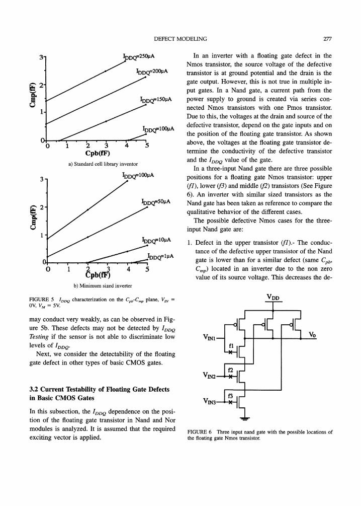
A CMOS static inverter chain with an open path in atransistor gate is considered. The electrical model ofthe faulty circuit is indicated in Figure 3, where thedefective transistor is located in the Nmos transistorof the first inverter and may be influenced by thevoltage at the metal track through the capacitive cou-
pling. Large opens are assumed so that the poly trackcannot be influenced significantly by the input signal(VIN). First, the transfer capabilities Vo versus VINand IDD versus VIN of the defective inverter are ex-amined (label IDo is used for the quiescent current
varying with the power supply). Next, the quiescentpower supply current consumption in terms of thedefect parameters (Cpb, Cmp) is characterized.
In an inverter with a floating gate defect in theNmos transistor, when VIN is zero Volts there willexist a low impedance path from the power supply to
ground if the floating gate gets enough voltage. Thissituation can be observed in Figure 4, where typical
276 V.H. CHAMPAC and J. FIGUERAS
vIN 1v.__q |
Cpb__
VDD
FIGURE 3 Inverter with a floating gate Nmos transistor.
curves for the output voltage Vo of the defective in-verter and the power supply current (IDD) are shown.For VN 0V, the output voltage of the faulty in-verter is lowered (See Figure 4) but it can be inter-preted as a "good high logic level" by the next stagefor a wide range of the defect parameters [3] [5] [13].
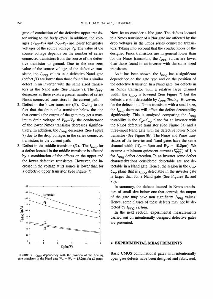
Taking into account that a fraction of the outputvoltage is induced at the floating gate, the outputvoltage and the power supply current (IDD) of thedefective transistor decrease as VtN increases (SeeFigure 4). However, Vo does not discharge com-pletely to ground; it remains charged, if leakages arenot taken into account, to a certain value. At that
5 Vo 20
4
IDD
i 3 4VIN(V)
16
12 <.8
FIGURE 4 Typical Spice transfer curves for an inverter with afloating gate Nmos transistor.
remanent Vo value, it is induced the threshold voltageat the floating gate transistor [5]. The intermediatevoltage may be interpreted as a high or a low logiclevel by the next stage depending on its thresholdgate voltage. This depends on the relative sizes of thePmos and Nmos transistors and on type of gate. Dueto this, Logic Testing based on the stuck-open modelmay not detect some classes (Cpb, Crop) of floatinggate defects [3] [5] [9]. When the floating poly issignificantly influenced by a metal track Crop, thevoltage at the output of the defective inverter may be
discharged very close to ground [5].Now, the IDDa detectability of the floating gate de-
fect located in an Nmos transistor of an inverter chainis investigated. In this test methodology, the defect isexcited by an input vector that creates a low imped-ance path from the power supply to ground if thefloating gate gets enough voltage. For the invertercase, the input vector is VIN 0V. The quiescentpower supply current consumption IDDa is character-ized in terms of the defect parameters Cpb and Crop.We consider two inverters with different sized tran-sistors. One of them corresponds to a symmetric in-verter of a minimum size allowed by the technology(ES2’s Dual Layer Metal, 1.5 pm, n-Well CMOS) WN3pm and Wp 10.8pm. The other corresponds to
an inverter from the ES2’s library (same technologyas before)WN We 15.2pro.The values of the capacitances Cpb and Cmp deter-
mine the degree of conduction of the floating gatetransistor. Depending on Cpb and Crop values, the qui-escent power supply current through the inverter canbe estimated. For the standard cell inverter, signifi-cant IDD0 values exist in the entire range (0 -< Cpb <--5fF, 0 <-- Cmp <- 3fF) of the defect parameters (SeeFigures 3 and 5a). It must be noted that even for theworst case defect parameters (Crop 0 and Cpblarge), high values of lopO are found. Hence, thefloating gate defects located in this inverter are de-tectable by IDDO Testing.
For the minimum sized inverter, a large class of thefloating defects may be detected by Current Testing(See Figure 5b). The IDDO depends on the defect pa-rameters. For large values of Cpb, the floating gatetransistor may operate in the subthreshold region or
DEFECT MODELING 277
IDDQ=2S0A
IDDQ=200A
I
IDDQ=150pA
00
2
IDDQ=100A
1 2 3 4 5Cpb(fF)
a) Standard cell library inventor
IDDQ=1001aA
IDDQ=501A
1,
0 1 pb(t__ 4 5
b) Minimum sized inverter
FIGURE 5 Iooa characterization on the Cpb-fmp plane, Vm0v, vM 5v.
may conduct very weakly, as can be observed in Fig-ure 5b. These defects may not be detected by IDDaTesting if the sensor is not able to discriminate lowlevels of IDDQ.
Next, we consider the detectability of the floatinggate defect in other types of basic CMOS gates.
3.2 Current Testability of Floating Gate Defectsin Basic CMOS Gates
In this subsection, the IDoQ dependence on the posi-tion of the floating gate transistor in Nand and Normodules is analyzed. It is assumed that the requiredexciting vector is applied.
In an inverter with a floating gate defect in theNmos transistor, the source voltage of the defectivetransistor is at ground potential and the drain is thegate output. However, this is not true in multiple in-
put gates. In a Nand gate, a current path from thepower supply to ground is created via series con-nected Nmos transistors with one Pmos transistor.Due to this, the voltages at the drain and source of thedefective transistor, depend on the gate inputs and onthe position of the floating gate transistor. As shownabove, the voltages at the floating gate transistor de-termine the conductivity of the defective transistorand the IDDa value of the gate.
In a three-input Nand gate there are three possiblepositions for a floating gate Nmos transistor: upper(fl), lower (f3) and middle (f2) transistors (See Figure6). An inverter with similar sized transistors as theNand gate has been taken as reference to compare thequalitative behavior of the different cases.The possible defective Nmos cases for the three-
input Nand gate are"
1. Defect in the upper transistor (fl).- The conduc-tance of the defective upper transistor of the Nandgate is lower than for a similar defect (same Cpb,Crop) located in an inverter due to the non zerovalue of its source voltage. This decreases the de-
VDD
FIGURE 6 Three input nand gate with the possible locations ofthe floating gate Nmos transistor.
278 V.H. CHAMPAC and J. FIGUERAS
gree of conduction of the defective upper transis-tor owing to the body effect. In addition, the volt-ages (VFo.--Vs) and (Vo-Vs) are lower for greatervoltages of the source voltage Vs The value of thesource voltage depends on the number of seriesconnected transistors from the source of the defec-tive transistor to ground. Due to the non zerovalue of the source voltage of the defective tran-
sistor, the IDDQ values in a defective Nand gate(defectf/) are lower than those found for a similardefect in an inverter with the same sized transis-tors as the Nand gate (See Figure 7). The IDDadecreases as there exists a greater number of seriesNmos connected transistors in the current path.Defect in the lower transistor (f3).- Owing to thefact that the drain of a transistor below the onethat controls the output of the gate may get a max-imum drain voltage of Voo-Vr, the conductanceof the lower Nmos transistor decreases significa-tively. In addition, the IDDa decreases (See Figure7) due to the drop voltages in the series connectedtransistors in the current path.Defect in the middle transistor (f2).- The IDDQ fora defect located in the middle transistor is affectedby a combination of the effects on the upper andthe lower defective transistors. However, the in-crease in the voltage at its source is lower than fora defective upper transistor (See Figure 7).
180
160
140
120
’--verter
f2
Cpb(fF)
FIGURE 7 IooQ dependency with the position of the floatinggate transistor in the Nand gate WN We 15.21arn for all gates.
Now, let us consider a Nor gate. The defects locatedin a Nmos transistor of a Nor gate are affected by thedrop voltages in the Pmos series connected transis-tors. Taking into account that the conductances of thedesigned Pmos transistors are in general lower thanfor the Nmos transistors, the IDDQ values are lowerthan those found in an inverter with the same sizedtransistors.As it has been shown, the IDDQ has a significant
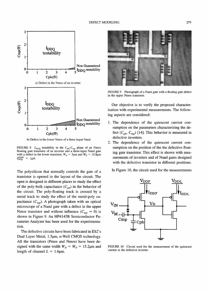
dependence on the gate type and on the position ofthe defective transistor. In a Nand gate, for defects inan Nmos transistor with a relative large channelwidth, the IDDa is lowered (See Figure 7) but thedefects are still detectable by IDDQ Testing. However,for the defects in a Nmos transistor with a small size,the IooQ decrease will affect the defect detectabilitysignificantly. This is analyzed comparing the IDDatestability in the Cpb-Cmp plane for an inverter withthe Nmos defective transistor (See Figure 8a) and a
three-input Nand gate with the defective lower Nmostransistor (See Figure 8b). The Nmos and Pmos tran-
sistors of the inverter and Nand gates have the samechannel width (WN 3gtm and Wp 10.8gtm). We
lmindetassume a minimum quiescent current -OOQ of 1for IooQ defect detection. In an inverter some defectcharacterizations considered detectable are not de-tectable in a Nand gate. Hence, the region in the Cpb-Crop plane that is IooQ detectable in the inverter gateis larger than for a Nand gate (See Figures 8a and8b).
In summary, the defects located in Nmos transis-tors of small size below one that controls the outputof the gate may have non significant IzzQ values.Hence, some classes of these defects may not be de-tected by Izo Testing.
In the next section, experimental measurementscarried out on intentionally designed defective gatesare presented.
4. EXPERIMENTAL MEASUREMENTS
Basic CMOS combinational gates with intentionallyopen gate defects have been designed and fabricated.
DEFECT MODELING 279
3
IDDQtestability
Non GuaranteedIDDQ testability
Cpb(fF)
a) Defect in the Nmos of an inverter
3
IDDQtestability
Non GuaranteedIDDQtestabilityi3 4 5
cpb(
b) Defect in the lower Nmos of a three imput Nand
FIGURE 8 !DDQ testability in the Cpb-Cmp plane of an Nmosfloating gate transistor of an inverter and a three-input Nand gatewith a defect in the lower transistor, WN 3pro and We 10.Spin
indet lpA.DQ
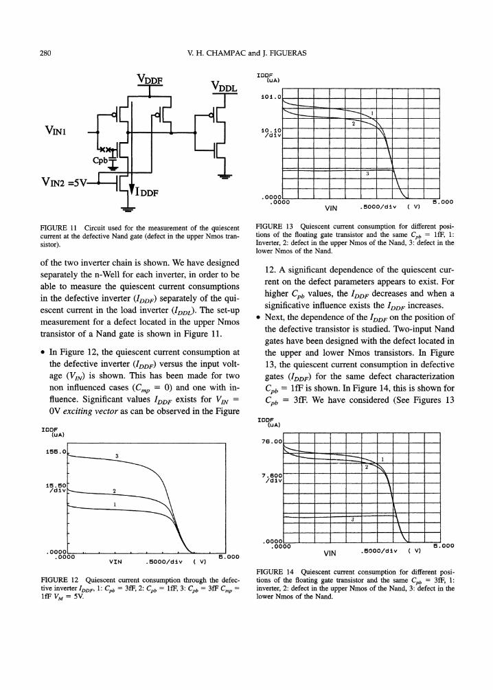
The polysilicon that normally controls the gate of atransistor is opened in the layout of the circuit. Theopen is designed in different places to study the effectof the poly-bulk capacitance (Cpb) in the behavior ofthe circuit. The poly-floating track is crossed by ametal track to study the effect of the metal-poly ca-
pacitance (C,np). A photograph taken with an opticalmicroscope of a Nand gate with a defect in the upperNmos transistor and without influence (Cmp 0) isshown in Figure 9. An HP4145B Semiconductor Pa-rameter Analyzer has been used for the experimenta-tion.The defective circuits have been fabricated in ES2’s
Dual Layer Metal, 1.5gm, n-Well CMOS technology.All the transistors (Pmos and Nmos) have been de-signed with the same width WN Wp 15.21am andlength of channel L 1.6m.
FIGURE 9 Photograph of a Nand gate with a floating gate defectin the upper Nmos transistor.
Our objective is to verify the proposed character-ization with experimental measurements. The follow-ing aspects are considered:
1. The dependence of the quiescent current con-
sumption on the parameters characterizing the de-fect (Cpb, Crop) [14]. This behavior is measured indefective inverters.
2. The dependence of the quiescent current con-
sumption on the position of the the defective float-ing gate transistor. This effect is shown with mea-surements of inverters and of Nand gates designedwith the defective transistor in different positions.
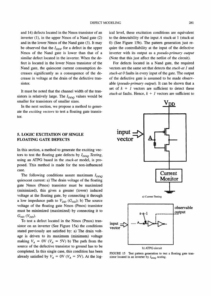
In Figure 10, the circuit used for the measurements
VDDF
IDDFVo
FIGURE 10 Circuit used for the measurement of the quiescentcurrent at the defective inverter.
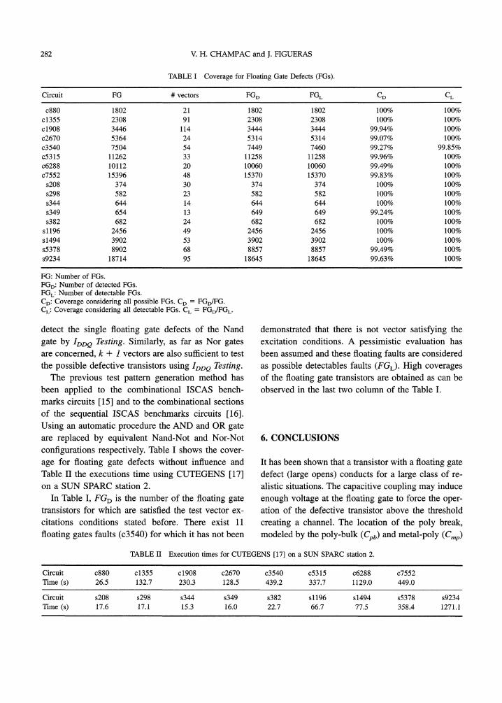
280 V.H. CHAMPAC and J. FIGUERAS
VIN1
VIN2
VDDF
IDDF
VDDL
.0000.0000 5. 000
VIN .5000/dv (V)
FIGURE 11 Circuit used for the measurement of the quiescentcurrent at the defective Nand gate (defect in the upper Nmos tran-sistor).
of the two inverter chain is shown. We have designedseparately the n-Well for each inverter, in order to beable to measure the quiescent current consumptionsin the defective inverter (IooF) separately of the qui-escent current in the load inverter (Iozr). The set-upmeasurement for a defect located in the upper Nmostransistor of a Nand gate is shown in Figure 11.
In Figure 12, the quiescent current consumption atthe defective inverter (IooF) versus the input volt-age (Vzv) is shown. This has been made for two
non influenced cases (Crop 0) and one with in-fluence. Significant values IOOF exists for Viv0V exciting vector as can be observed in the Figure
IDDF(uA)
:1.56.0
.0000.0000 .000
VIN .5000/dlv (V)
FIGURE 12 Quiescent current consumption through the defec-tive inverter IOOF, 1" Cpb 3fF, 2: Cpb lfF, 3: Cpb 3fF C,plfF V 5V.
FIGURE 13 Quiescent current consumption for different posi-tions of the floating gate transistor and the same Cpb lfF, 1"Inverter, 2: defect in the upper Nmos of the Nand, 3: defect in thelower Nmos of the Nand.
12. A significant dependence of the quiescent cur-rent on the defect parameters appears to exist. Forhigher Cpb values, the IooF decreases and when a
significative influence exists the IOF increases.Next, the dependence of the IooF on the position ofthe defective transistor is studied. Two-input Nandgates have been designed with the defect located inthe upper and lower Nmos transistors. In Figure13, the quiescent current consumption in defectivegates (IooF) for the same defect characterization
Cpb lfF is shown. In Figure 14, this is shown for
Cpb 3fF. We have considered (See Figures 13
IDDF(uA)
76.00
7.600--/dv
.0000.0000
VIN.000
5000/Cl:l,v V]
FIGURE 14 Quiescent current consumption for different posi-tions of the floating gate transistor and the same Cpb 3fF, 1:inverter, 2: defect in the upper Nmos of the Nand, 3: defect in thelower Nmos of the Nand.
DEFECT MODELING 281
and 14) defects located in the Nmos transistor of aninverter (1), in the upper Nmos of a Nand gate (2)and in the lower Nmos of the Nand gate (3). It maybe observed that the IDDe for a defect in the upperNmos of the Nand gate is lower than that of asimilar defect located in the inverter. When the de-fect is located in the lower Nmos transistor of theNand gate, the quiescent current consumption de-creases significantly as a consequence of the de-crease in voltage at the drain of the defective tran-
sistor.
It must be noted that the channel width of the tran-sistors is relatively large. The IDDQ values would besmaller for transistors of smaller sizes.
In the next section, we propose a method to gener-ate the exciting vectors to test a floating gate transis-tor.
5. LOGIC EXCITATION OF SINGLEFLOATING GATE DEFECTS
In this section, a method to generate the exciting vec-tors to test the floating gate defects by IDD2 Testing,using an ATPG based in the stuck-at model, is pro-posed. This method is made for the non-influencedcase.
The following conditions assure maximum IDDQ.quiescent current: a) The drain voltage of the floatinggate Nmos (Pmos) transistor must be maximized(minimized), this gives a greater (lower) inducedvoltage at the floating gate, by connecting it througha low impedance path to VDO (GND); b) The sourcevoltage of the floating gate Nmos (Pmos) transistormust be minimized (maximized) by connecting it to
GND (VDD).To test a defect located in the Nmos (Pmos) tran-
sistor on an inverter (See Figure 15a) the conditionsstated previously are satisfied by: a) The drain volt-age is driven to its maximum (minimum) voltagemaking VA 0V (VA 5V) b) The path from thesource of the defective transistor to ground has to becompleted. In this single case, this condition has beenalready satisfied by VA 0V (VA 5V). At the log-
ical level, these excitation conditions are equivalentto the detectability of the input A stuck-at 1 (stuck-at0) (See Figure 15b). The pattern generation just re-
quire the controllability at the input of the defectiveinverter with its output as a pseudo-primary output(Note that this just affect the netlist of the circuit).
For defects located in a Nand gate, the requiredvectors are the same set that detects the stuck-at I andstuck-at 0 faults in every input of the gate. The outputof the defective gate is assumed to be made observ-able (pseudo-primary output). It can be shown that aset of k + 1 vectors are sufficient to detect thesestuck-at faults. Hence, k + 1 vectors are sufficient to
VDD
inputvector A
CurrentMonitor
a) Current Testing
observables-a- 1 r
o__utput
vector
b) ATPG circuit
FIGURE 15 Test pattern generation to test a floating gate tran-sistor located in an inverter by IooQ testing.
282 V.H. CHAMPAC and J. FIGUERAS
Circuit FG
TABLE Coverage for Floating Gate Defects (FGs).
# vectors FGD FGL CD CLc880 1802
c1355 2308c1908 3446c2670 5364c3540 7504c5315 11262c6288 10112c7552 15396s208 374s298 582s344 644s349 654s382 682s1196 2456s1494 3902s5378 8902s9234 18714
21 1802 1802 100% 100%91 2308 2308 100% 100%114 3444 3444 99.94% 100%24 5314 5314 99.07% 100%54 7449 7460 99.27% 99.85%33 11258 11258 99.96% 100%20 10060 10060 99.49% 100%48 15370 15370 99.83% 100%30 374 374 100% 100%23 582 582 100% 100%14 644 644 100% 100%13 649 649 99.24% 100%24 682 682 100% 100%49 2456 2456 100% 100%53 3902 3902 100% 100%68 8857 8857 99.49% 100%95 18645 18645 99.63% 100%
FG: Number of FGs.FGD: Number of detected FGs.FGL: Number of detectable FGs.CD: Coverage considering all possible FGs. CD FGD/FG.C: Coverage considering all detectable FGs. C FGD/FGL.
detect the single floating gate defects of the Nandgate by IDDa Testing. Similarly, as far as Nor gatesare concerned, k + 1 vectors are also sufficient to testthe possible defective transistors using Izoa Testing.The previous test pattern generation method has
been applied to the combinational ISCAS bench-marks circuits [15] and to the combinational sectionsof the sequential ISCAS benchmarks circuits [16].Using an automatic procedure the AND and OR gateare replaced by equivalent Nand-Not and Nor-Notconfigurations respectively. Table I shows the cover-
age for floating gate defects without influence andTable II the executions time using CUTEGENS [17]on a SUN SPARC station 2.
In Table I, FGD is the number of the floating gatetransistors for which are satisfied the test vector ex-citations conditions stated before. There exist 11floating gates faults (c3540) for which it has not been
CircuitTime (s)
demonstrated that there is not vector satisfying theexcitation conditions. A pessimistic evaluation hasbeen assumed and these floating faults are consideredas possible detectables faults (FGL). High coveragesof the floating gate transistors are obtained as can beobserved in the last two column of the Table I.
6. CONCLUSIONS
It has been shown that a transistor with a floating gatedefect (large opens) conducts for a large class of re-alistic situations. The capacitive coupling may induceenough voltage at the floating gate to force the oper-ation of the defective transistor above the thresholdcreating a channel. The location of the poly break,modeled by the poly-bulk (Cpb) and metal-poly (Cmp)
TABLE II Execution times for CUTEGENS [17] on a SUN SPARC station 2.
c880 c1355 c1908 c2670 c3540 c5315 c6288 c755226.5 132.7 230.3 128.5 439.2 337.7 1129.0 449.0
Circuit s208 s298 s344 s349 s382 1196 1494 s5378 s9234Time (s) 17.6 17.1 15.3 16.0 22.7 66.7 77.5 358.4 1271.1
DEFECT MODELING 283
capacitances determines the IDDQ of the defective
gate. In addition, the Iooa depends on the position ofthe floating gate transistor in the defective gate con-sidered. It has been shown that defective floating gatetransistors of small size, located below the one con-
trolling the output of the gate give lower levels of
IDDQ. Experimental data on defective circuits withdifferent locations of the breaks have been obtained.The measured quiescent current depends on the breaklocation and on the position of the defective floatinggate transistor in each type of gate studied. The mea-surements show good agreement with the predicted
IDDQ levels for the circuits analyzed. The requiredexcitation conditions of the floating gate defects hasbeen translated to the stuck-at controllability at theinputs of the gate. This allows the generation of theexcitation vectors to test the floating gate defects by
IDDQ Testing using a conventional ATPG. In general,gates (inverter, Nand, Nor) with k inputs need k + 1vectors to test the possible floating gate transistor.
Acknowledgements
The authors thank Eugenio Isem for providing datafault simulation using CUTEGENS. This work hasbeen partially supported by the ProjectARCHIMEDES (ESPRIT III Basic Research ProjectNo 7107) and by the Comisi6n Interministerial parala Ciencia y Tecnologia(CICYT) No TIC 94-0561.
References[1] Renovell, M. and Cambon, G. (1986). "Topology Depen-
dence of Floating Gate Faults in MOS Circuits", ElectronicsLetters, Vol.22, No 3, (January), pp. 152-153.
[2] Maly, W., Nag, P. K. and Nigh, P. (1988). "Testing OrientedAnalysis of CMOS ICs with Opens", Prec. Int. Conf. onComputer-Aided Design, pp. 344-347.
[3] Champac, V. H., Rodrfgues-Montafi6s, R., Segura, J. A.,Figueras, J. and Rubio, J. A. (1991). "Fault Modelling ofGate Oxide Short, Floating Gate and Bridging Failures inCMOS Circuits", European Test Conference, pp. 143-148.
[4] Renovell, M. and Cambon, G. (1992). "Electrical Analysisand Modeling of Floating-Gate Fault", IEEE Transactionson Computer-Aided Design, Vol. 11, No. 11, (November),pp. 1450-1458.
[5] Victor H. Champac, (1993). "Caracterizaci6n del defecto depuerta flotante y su detecci6n en circuitos CMOS digitales",
Ph.D. dissertation, Universitat Politcnica de Catalunya,Spain, March.
[6] Maly, W. (1985). "Modelling of Lithography Related YieldLosses for CAD of VLSI Circuits", IEEE Transactions onComputer-Aided Design, Vol. CAD-4, No. 3, (July), pp.166-177.
[7] Henderson, C. L., Soden, J. M. and Hawkins, C. F. (1991)."The behavior and Testing Implications of CMOS IC LogicGate Open Circuits", International Test Conference, pp.302-310.
[8] Wadsack, R. L. (1978). "Fault Modeling and Logic Simula-tion of CMOS and MOS Integrated Circuits", The Bell Sys-tem Technical Journal, vol.57, (May-June), pp. 1449-1474.
[9] Champac, Victor H., Rubio, J. A. and Figueras, J. (1994)."Electrical Model of the Floating Gate Defect in CMOSICs: Implications on IooQ Testing", IEEE Transactions onComputer-Aided Design, Vol. 13, (March), pp. 359-369.
[10] Maly, W. and Nigh, P. (1988). "Built-In Current Testing:Feasibility Study", Prec. Int. Conf. on Computer-Aided De-sign, pp. 340-343.
[11] Hawkins, C. E, Soden, J. M., Fritzemeier R. R. and Hom-ing, L. K. (1989). "Quiescent Power Supply Current Mea-surement for CMOS IC Detection", IEEE Transactions onIndustrial Electronics, Vol. 36, No. 2, (May), pp. 211-218
[12] Soden, J. M., Hawkins, C. E, Gulati R. K. and Mao, W.(1992). "lope Testing: A Review", J. Electronic Testing:Theory and Applications (Jetta), Vol. 3, No. 4, (December),pp. 291-303.
[13] Rodrfguez-Montafi6s, R., Segura, J. A., Champac, V. H.,Figueras, J. and Ruble, J. A. (1991). "Current vs Logic Test-ing of Gate Oxide Short, Floating Gate and Bridging Fail-ures in CMOS", International Test Conference, pp. 510-519.
[14] Segura, J. A., "Champac, V. H., Rodrfguez-Montafi6s,Figueras, J. and Rubio, J. A. (1992). "Quiescent CurrentAnalysis and Experimentation of Defective CMOS Cir-cuits", J. Electronic Testing: Theory and Applications(Jetta), Vol. 3, No. 4, (December), pp. 337-348.
[15] Brglez F. and Fujiwara, H. (1985). "A neutral neflist of 10combinational benchmark circuits and a target translator infortran", IEEE Int. Symp. on Circuits and Systems, pp. 663-698.
[16] Brglez, E, Bryan D. and Kozminski, K. (1989). "Combina-tional Profiles of Sequential Benchmark Circuits", IEEEInt’l Syrup. on Circuits and Systems, pp. 1929-1934.
17] Isem, Eugenio and Figueras, Joan, (1993). "Test Generationwith High Coverages for Quiescent Current Test of BridgingFaults in Combinational Circuits", International Test Con-ference, pp 73-82.
Authors’ Biographies
Victor H. Champac was born in Peni in 1964. Hereceived the Electronic Engineering degree from theUniversidad Aut6noma de Nuevo Le6n (M6xico) andthe Ph.D. degree (Electronic Technology) from theUniversitat Politcnica de Catalunya (UPC), Spain.From 1988 to 1993, he was associate professor of theElectronic Engineering Department at the UPC. He is

284 V.H. CHAMPAC and J. FIGUERAS
currently titular professor at the Instituto Nacional deAstrofisica, Optica y Electr6nica-INAOE (Mexico).His research interests include VLSI design and test,defect and fault models and testing mixed signal cir-cuits.
Joan Figueras received his Industrial Engineering(Electrical) degree from the Universitat Politcnicade Catalunya and the Ms.C. (Electrical) and Ph.D.(Computer Information and Control) degrees from
the University of Michigan were he was a FullbrightScholar and worked in the Systems Engineering Lab-oratory (1968-71) Since 1983 is Professor at the De-partment of Electronic Engineering of the U.P.C. with
teaching and research responsibilities in the area ofDigital Systems and VLSI design. His current re-search include Test and Design for Testability, Defectand Fault Models and Testing and Fault Tolerancemethodologies for emerging technologies.

International Journal of
AerospaceEngineeringHindawi Publishing Corporationhttp://www.hindawi.com Volume 2010
RoboticsJournal of
Hindawi Publishing Corporationhttp://www.hindawi.com Volume 2014
Hindawi Publishing Corporationhttp://www.hindawi.com Volume 2014
Active and Passive Electronic Components
Control Scienceand Engineering
Journal of
Hindawi Publishing Corporationhttp://www.hindawi.com Volume 2014
International Journal of
RotatingMachinery
Hindawi Publishing Corporationhttp://www.hindawi.com Volume 2014
Hindawi Publishing Corporation http://www.hindawi.com
Journal ofEngineeringVolume 2014
Submit your manuscripts athttp://www.hindawi.com
VLSI Design
Hindawi Publishing Corporationhttp://www.hindawi.com Volume 2014
Hindawi Publishing Corporationhttp://www.hindawi.com Volume 2014
Shock and Vibration
Hindawi Publishing Corporationhttp://www.hindawi.com Volume 2014
Civil EngineeringAdvances in
Acoustics and VibrationAdvances in
Hindawi Publishing Corporationhttp://www.hindawi.com Volume 2014
Hindawi Publishing Corporationhttp://www.hindawi.com Volume 2014
Electrical and Computer Engineering
Journal of
Advances inOptoElectronics
Hindawi Publishing Corporation http://www.hindawi.com
Volume 2014
The Scientific World JournalHindawi Publishing Corporation http://www.hindawi.com Volume 2014
SensorsJournal of
Hindawi Publishing Corporationhttp://www.hindawi.com Volume 2014
Modelling & Simulation in EngineeringHindawi Publishing Corporation http://www.hindawi.com Volume 2014
Hindawi Publishing Corporationhttp://www.hindawi.com Volume 2014
Chemical EngineeringInternational Journal of Antennas and
Propagation
International Journal of
Hindawi Publishing Corporationhttp://www.hindawi.com Volume 2014
Hindawi Publishing Corporationhttp://www.hindawi.com Volume 2014
Navigation and Observation
International Journal of
Hindawi Publishing Corporationhttp://www.hindawi.com Volume 2014
DistributedSensor Networks
International Journal of