Embed Size (px)
Citation preview
UC1842A/3A/4A/5AUC2842A/3A/4A/5AUC3842A/3A/4A/5A
SLUS224A - SEPTEMBER 1994 - REVISED APRIL 2002
• Optimized for Off-line and DC to DCConverters
• Low Start Up Current (<0.5mA)
• Trimmed Oscillator Discharge Current
• Automatic Feed Forward Compensation
• Pulse-by-Pulse Current Limiting
• Enhanced Load Response Characteristics
• Under-Voltage Lockout With Hysteresis
• Double Pulse Suppression
• High Current Totem Pole Output
• Internally Trimmed Bandgap Reference
• 500kHz Operation
• Low RO Error Amp
Current Mode PWM Controller
The UC1842A/3A/4A/5A family of control ICs is a pin for pin compati-ble improved version of the UC3842/3/4/5 family. Providing the nec-essary features to control current mode switched mode powersupplies, this family has the following improved features. Start up cur-rent is guaranteed to be less than 0.5mA. Oscillator discharge istrimmed to 8.3mA. During under voltage lockout, the output stagecan sink at least 10mA at less than 1.2V for VCC over 5V.
The difference between members of this family are shown in the tablebelow.
BLOCK DIAGRAM
FEATURES DESCRIPTION
applicationINFOavailable
Part # UVLO On UVLO Off Maximum DutyCycle
UC1842A 16.0V 10.0V <100%
UC1843A 8.5V 7.9V <100%
UC1844A 16.0V 10.0V <50%
UC1845A 8.5V 7.9V <50%
Note 1: A = DIL-8 Pin Number. B = SO-14 Pin Number.Note 2: Toggle flip flop used only in 1844A and 1845A.
A/B
2
UC1842A/3A/4A/5AUC2842A/3A/4A/5AUC3842A/3A/4A/5A
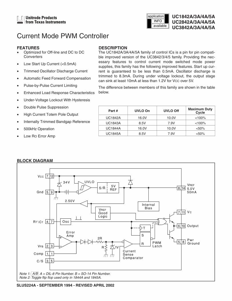
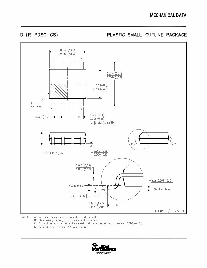
DIL-8, SOIC-8 (TOP VIEW)J or N, D8 Package
CONNECTION DIAGRAMS
ABSOLUTE MAXIMUM RATINGS (Note 1)
Note 1. All voltages are with respect to Ground, Pin 5. Currentsare positive into, negative out of the specified terminal. ConsultPackaging Section of Databook for thermal limitations and con-siderations of packages. Pin numbers refer to DIL package only.
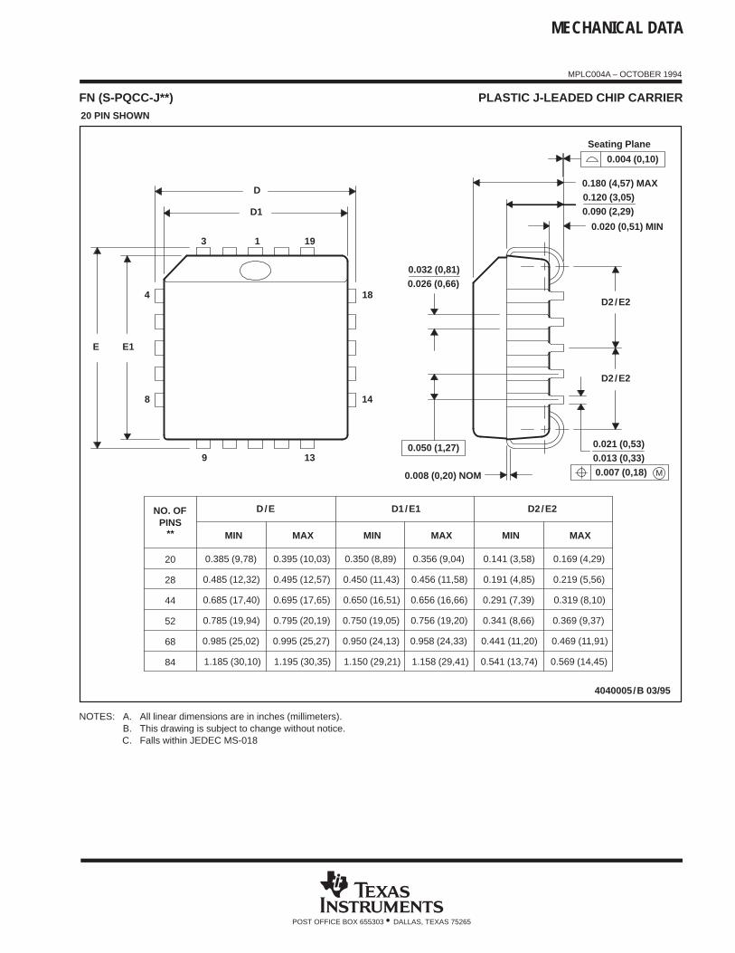
PLCC-20, LCC-20(TOP VIEW)Q, L Packages
Supply Voltage (Low Impedance Source) . . . . . . . . . . . . . . 30VSupply Voltage (ICC mA) . . . . . . . . . . . . . . . . . . . . Self LimitingOutput Current. . . . . . . . . . . . . . . . . . . . . . . . . . . . . . . . . . . ±1AOutput Energy (Capacitive Load). . . . . . . . . . . . . . . . . . . . . 5µJAnalog Inputs (Pins 2, 3). . . . . . . . . . . . . . . . . . . -0.3V to +6.3VError Amp Output Sink Current . . . . . . . . . . . . . . . . . . . . 10mAPower Dissipation at TA ≤ 25°C (DIL-8) . . . . . . . . . . . . . . . . 1WStorage Temperature Range. . . . . . . . . . . . . . -65°C to +150°CLead Temperature (Soldering, 10 Seconds) . . . . . . . . . . 300°C
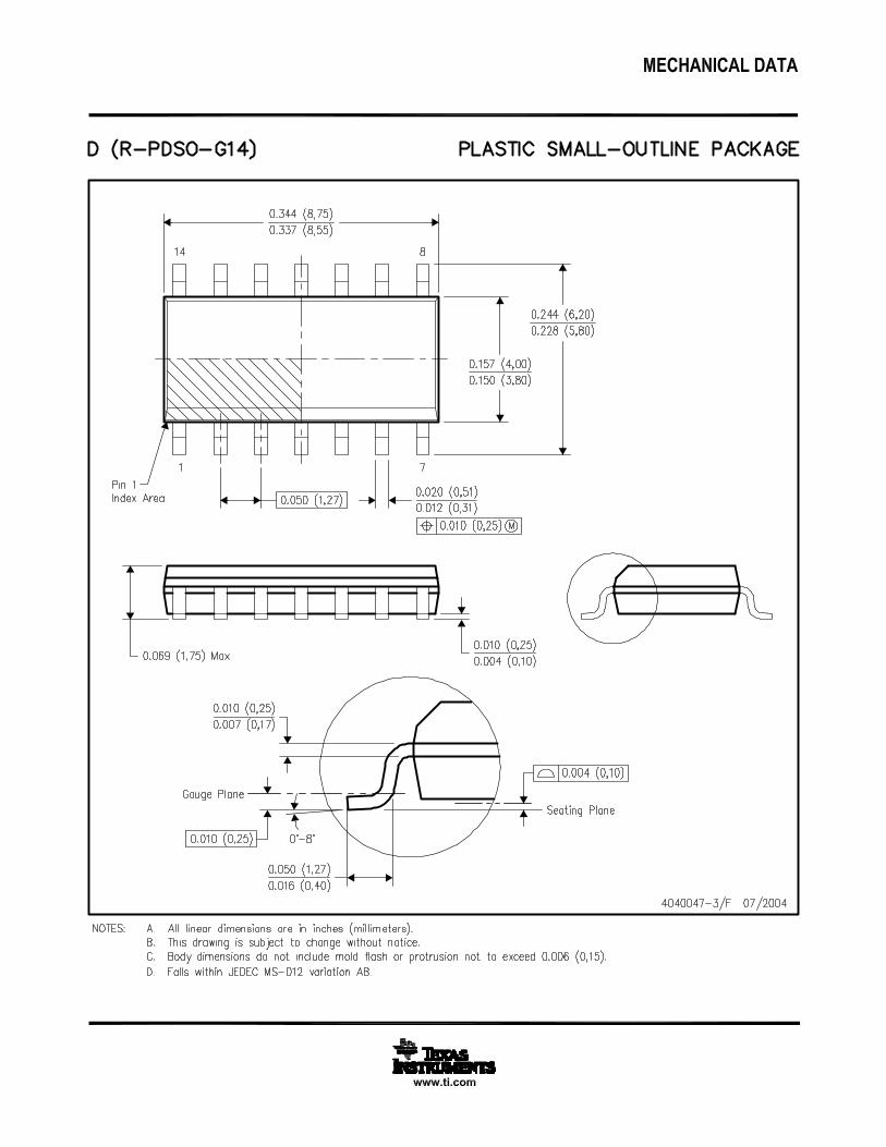
SOIC-14 (TOP VIEW)D Package
PACKAGE PIN FUNCTIONFUNCTION PIN
N/C 1Comp 2N/C 3-4VFB 5N/C 6ISENSE 7N/C 8-9RT/CT 10N/C 11Pwr Gnd 12Gnd 13N/C 14Output 15N/C 16VC 17VCC 18N/C 19VREF 20
N/C
VREF
VCC
OUTPUT
VCC
GND
1
2
3
4
5
6
7
8
16
15
14
13
12
11
N/C
N/C
N/C
RT/CT
N/C
COMP
VFB
ISENSE
PWRGND
N/C
10
9
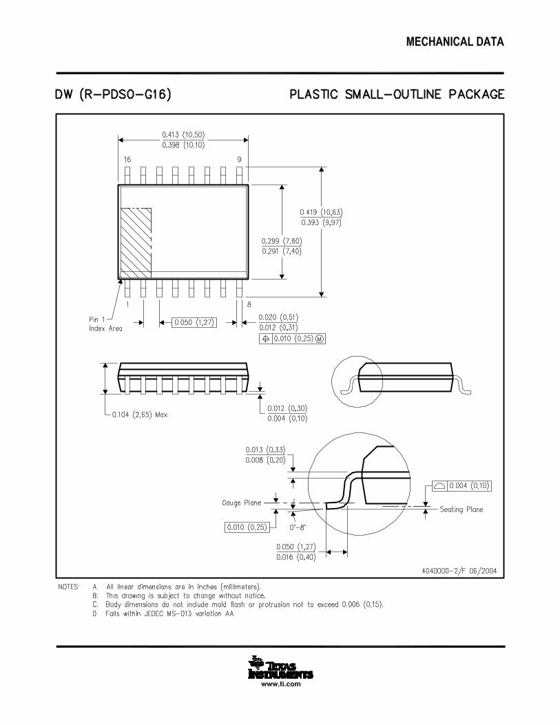
SOIC-WIDE16 (TOP VIEW)DW Package
3
UC1842A/3A/4A/5AUC2842A/3A/4A/5AUC3842A/3A/4A/5A
PARAMETER TEST CONDITIONSUC184xA\UC284xA UC384xA
UNITSMIN. TYP. MAX. MIN. TYP. MAX.
Reference SectionOutput Voltage TJ = 25°C, IO = 1mA 4.95 5.00 5.05 4.90 5.00 5.10 V
Line Regulation 12 ≤ VIN 25V 6 20 6 20 mV
Load Regulation 1 ≤ IO ≤ 20mA 6 25 6 25 mV
Temp. Stability (Note 2, Note 7) 0.2 0.4 0.2 0.4 mV/°C
Total Output Variation Line, Load, Temp. 4.9 5.1 4.82 5.18 V
Output Noise Voltage 10Hz ≤ f ≤ 10kHz
TJ = 25°C (Note 2) 50 50 µV
Long Term Stability TA = 125°C, 1000Hrs. (Note 2) 5 25 5 25 mV
Output Short Circuit -30 -100 -180 -30 -100 -180 mA
Oscillator SectionInitial Accuracy TJ = 25°C (Note 6) 47 52 57 47 52 57 kHz
Voltage Stability 12 ≤ VCC ≤ 25V 0.2 1 0.2 1 %
Temp. Stability TMIN ≤ TA ≤ TMAX (Note 2) 5 5 %
Amplitude VPIN 4 peak to peak (Note 2) 1.7 1.7 V
Discharge Current TJ = 25°C, VPIN 4 = 2V (Note 8) 7.8 8.3 8.8 7.8 8.3 8.8 mA
VPIN 4 = 2V (Note 8) 7.5 8.8 7.6 8.8 mA
Error Amp SectionInput Voltage VPIN 1 = 2.5V 2.45 2.50 2.55 2.42 2.50 2.58 V
Input Bias Current -0.3 -1 -0.3 -2 µA
AVOL 2 ≤ VO ≤ 4V 65 90 65 90 dB
Unity Gain Bandwidth TJ = 25°C (Note 2) 0.7 1 0.7 1 MHz
PSRR 12 ≤ VCC ≤ 25V 60 70 60 70 dB
Output Sink Current VPIN 2 = 2.7V, VPIN 1 = 1.1V 2 6 2 6 mA
Output Source Current VPIN 2 = 2.3V, VPIN 1 = 5V -0.5 -0.8 -0.5 -0.8 mA
VOUT High VPIN 2 = 2.3V, RL = 15k to ground 5 6 5 6 V
VOUT Low VPIN 2 = 2.7V, RL = 15k to Pin 8 0.7 1.1 0.7 1.1 V
Current Sense SectionGain (Note 3, Note 4) 2.85 3 3.15 2.85 3 3.15 V/V
Maximum Input Signal VPIN 1 = 5V (Note 3) 0.9 1 1.1 0.9 1 1.1 V
PSRR 12 ≤ VCC ≤ 25V (Note 3) 70 70 dB
Input Bias Current -2 -10 -2 -10 µA
Delay to Output VPIN 3 = 0 to 2V (Note 2) 150 300 150 300 ns
Output SectionOutput Low Level ISINK = 20mA 0.1 0.4 0.1 0.4 V
ISINK = 200mA 15 2.2 15 2.2 V
Output High Level ISOURCE = 20mA 13 13.5 13 13.5 V
ISOURCE = 200mA 12 13.5 12 13.5 V
Rise Time TJ = 25°C, CL = 1nF (Note 2) 50 150 50 150 ns
Fall Time TJ = 25°C, CL = 1nF (Note 2) 50 150 50 150 ns
UVLO Saturation VCC = 5V, ISINK = 10mA 0.7 1.2 0.7 1.2 V
ELECTRICAL CHARACTERISTICS Unless otherwise stated, these specifications apply for –55°C ≤ TA ≤ 125°C for theUC184xA; –40°C ≤ TA ≤ 125°C for the UC284xAQ; –40°C ≤ TA ≤ 85°C for the UC284xA; 0 ≤ TA ≤ 70°C for the UC384xA; VCC = 15V(Note 5); RT = 10k; CT = 3.3nF; TA = TJ; Pin numbers refer to DIL-8.
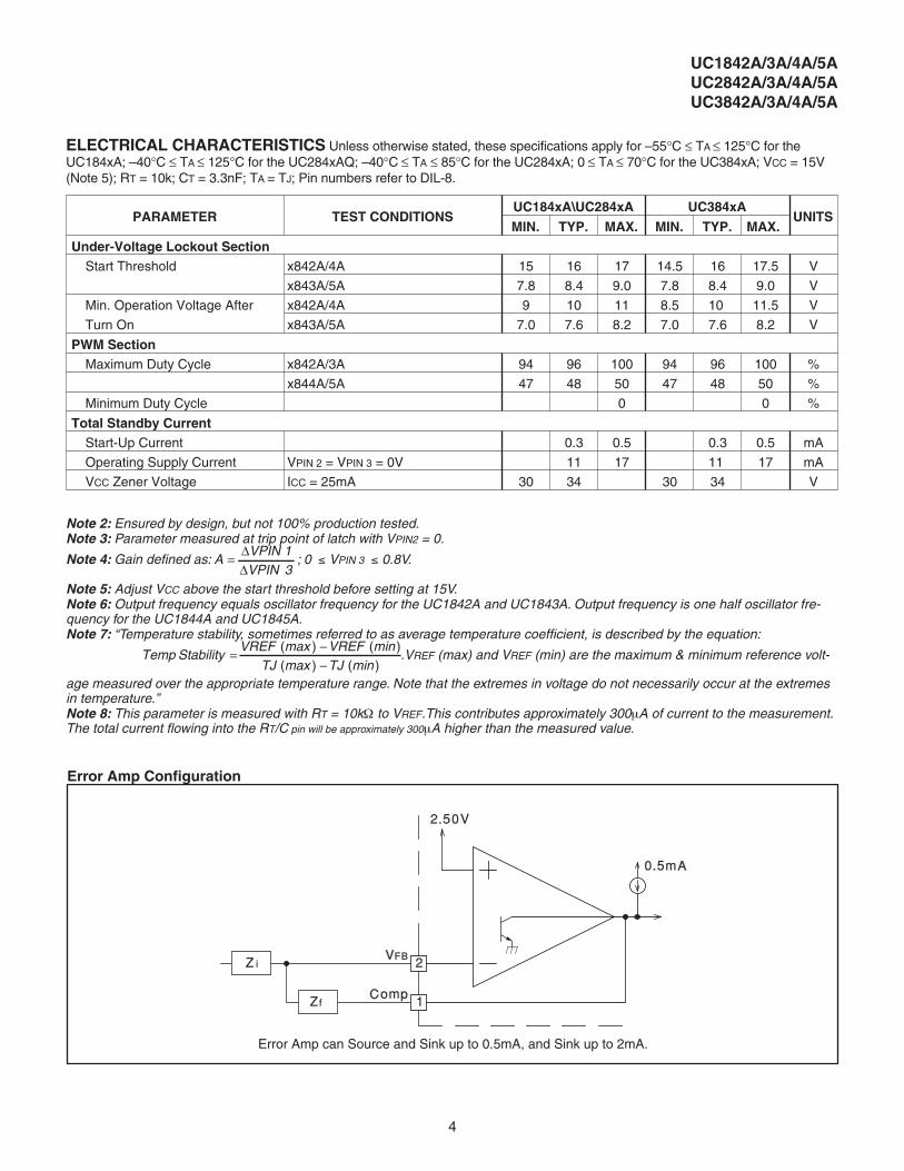
4
UC1842A/3A/4A/5AUC2842A/3A/4A/5AUC3842A/3A/4A/5A
PARAMETER TEST CONDITIONSUC184xA\UC284xA UC384xA
UNITSMIN. TYP. MAX. MIN. TYP. MAX.
Under-Voltage Lockout SectionStart Threshold x842A/4A 15 16 17 14.5 16 17.5 V
x843A/5A 7.8 8.4 9.0 7.8 8.4 9.0 V
Min. Operation Voltage After x842A/4A 9 10 11 8.5 10 11.5 V
Turn On x843A/5A 7.0 7.6 8.2 7.0 7.6 8.2 V
PWM SectionMaximum Duty Cycle x842A/3A 94 96 100 94 96 100 %
x844A/5A 47 48 50 47 48 50 %
Minimum Duty Cycle 0 0 %
Total Standby CurrentStart-Up Current 0.3 0.5 0.3 0.5 mA
Operating Supply Current VPIN 2 = VPIN 3 = 0V 11 17 11 17 mA
VCC Zener Voltage ICC = 25mA 30 34 30 34 V
Note 2: Ensured by design, but not 100% production tested.Note 3: Parameter measured at trip point of latch with VPIN2 = 0.
Note 4: Gain defined as: AVPINVPIN
= ∆∆
13
; 0 VPIN 3 0.8V.
Note 5: Adjust VCC above the start threshold before setting at 15V.Note 6: Output frequency equals oscillator frequency for the UC1842A and UC1843A. Output frequency is one half oscillator fre-quency for the UC1844A and UC1845A.Note 7: “Temperature stability, sometimes referred to as average temperature coefficient, is described by the equation:
Temp StabilityVREF max VREF min
TJ max TJ min= −
−( ) ( )( ) ( )
.VREF (max) and VREF (min) are the maximum & minimum reference volt-
age measured over the appropriate temperature range. Note that the extremes in voltage do not necessarily occur at the extremesin temperature.”Note 8: This parameter is measured with RT = 10k to VREF.This contributes approximately 300 A of current to the measurement.The total current flowing into the RT/C pin will be approximately 300 A higher than the measured value.
ELECTRICAL CHARACTERISTICS Unless otherwise stated, these specifications apply for –55°C ≤ TA ≤ 125°C for theUC184xA; –40°C ≤ TA ≤ 125°C for the UC284xAQ; –40°C ≤ TA ≤ 85°C for the UC284xA; 0 ≤ TA ≤ 70°C for the UC384xA; VCC = 15V(Note 5); RT = 10k; CT = 3.3nF; TA = TJ; Pin numbers refer to DIL-8.
Error Amp Configuration
Error Amp can Source and Sink up to 0.5mA, and Sink up to 2mA.
5
UC1842A/3A/4A/5AUC2842A/3A/4A/5AUC3842A/3A/4A/5A
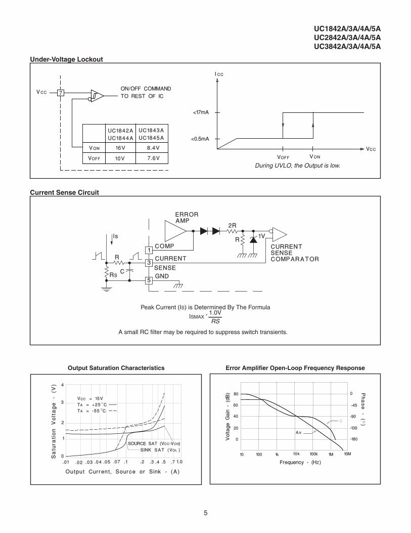
Under-Voltage Lockout
During UVLO, the Output is low.
Current Sense Circuit
A small RC filter may be required to suppress switch transients.
Peak Current (IS) is Determined By The Formula
ISMAX ′ 1.0VRS
Error Amplifier Open-Loop Frequency ResponseOutput Saturation Characteristics
6
UC1842A/3A/4A/5AUC2842A/3A/4A/5A
APPLICATIONS DATA (cont.)
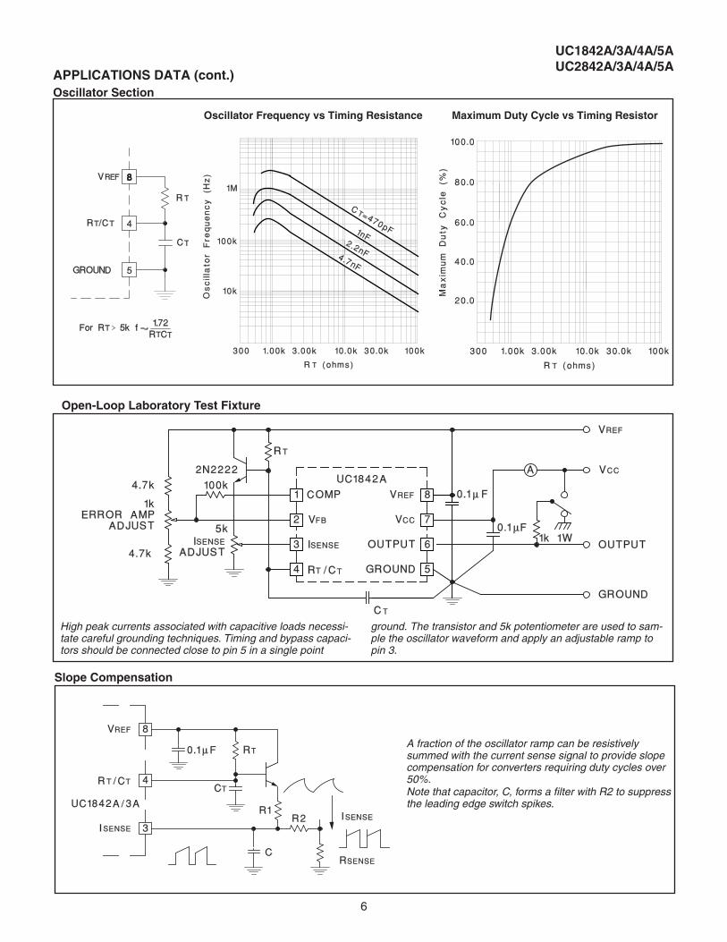
Open-Loop Laboratory Test Fixture
Oscillator Section
Oscillator Frequency vs Timing Resistance Maximum Duty Cycle vs Timing Resistor
High peak currents associated with capacitive loads necessi-tate careful grounding techniques. Timing and bypass capaci-tors should be connected close to pin 5 in a single point
ground. The transistor and 5k potentiometer are used to sam-ple the oscillator waveform and apply an adjustable ramp topin 3.
Slope Compensation
A fraction of the oscillator ramp can be resistivelysummed with the current sense signal to provide slopecompensation for converters requiring duty cycles over50%.Note that capacitor, C, forms a filter with R2 to suppressthe leading edge switch spikes.
7
UC1842A/3A/4A/5AUC2842A/3A/4A/5AUC3842A/3A/4A/5A
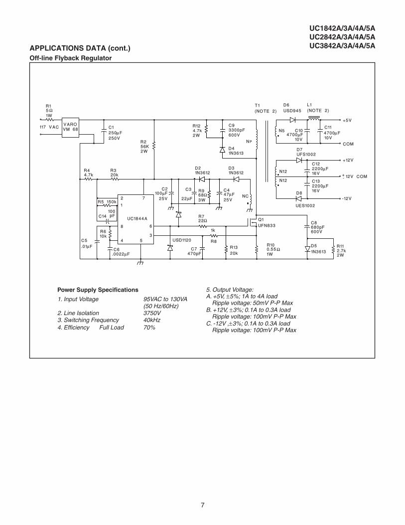
Off-line Flyback RegulatorAPPLICATIONS DATA (cont.)
Power Supply Specifications
1. Input Voltage 95VAC to 130VA(50 Hz/60Hz)
2. Line Isolation 3750V3. Switching Frequency 40kHz4. Efficiency Full Load 70%
5. Output Voltage:A. +5V, ±5%; 1A to 4A load
Ripple voltage: 50mV P-P MaxB. +12V, ±3%; 0.1A to 0.3A load
Ripple voltage: 100mV P-P MaxC. -12V ,±3%; 0.1A to 0.3A load
Ripple voltage: 100mV P-P Max
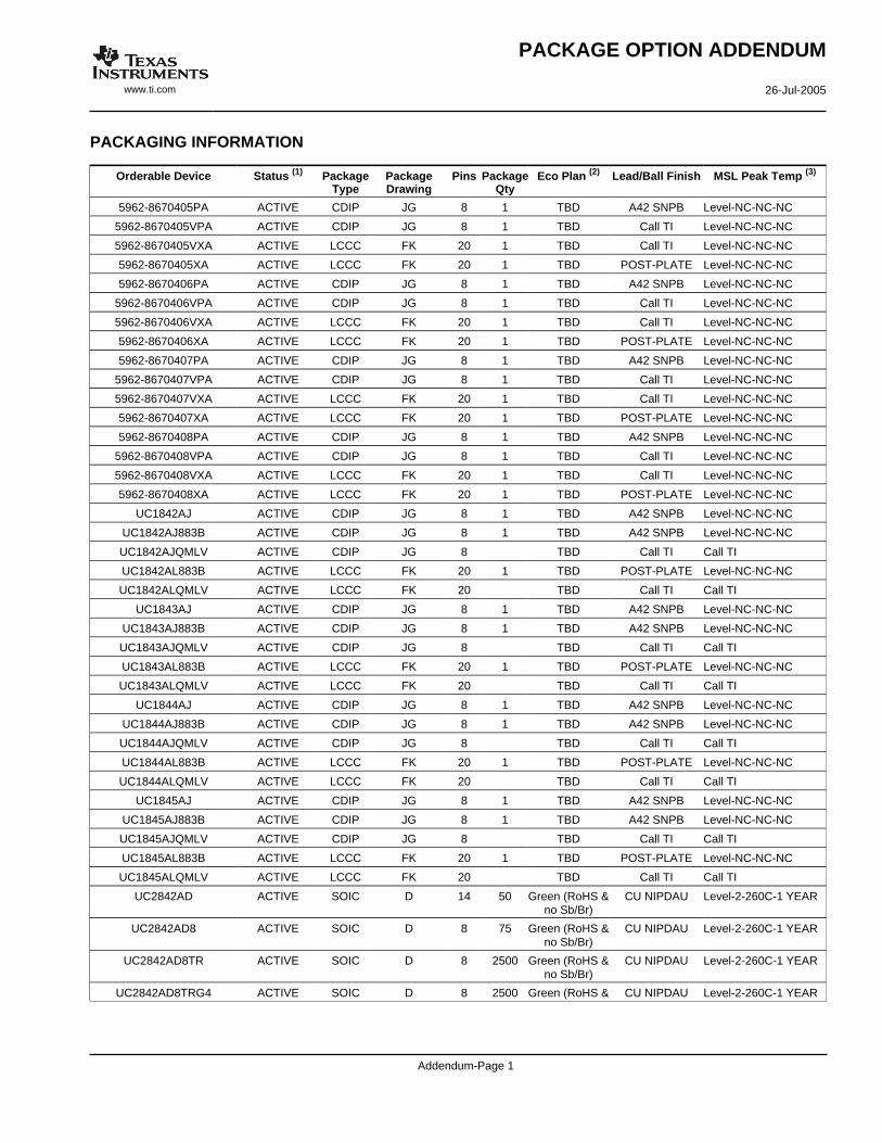
PACKAGING INFORMATION
Orderable Device Status (1) PackageType
PackageDrawing
Pins PackageQty
Eco Plan (2) Lead/Ball Finish MSL Peak Temp (3)
5962-8670405PA ACTIVE CDIP JG 8 1 TBD A42 SNPB Level-NC-NC-NC
5962-8670405VPA ACTIVE CDIP JG 8 1 TBD Call TI Level-NC-NC-NC
5962-8670405VXA ACTIVE LCCC FK 20 1 TBD Call TI Level-NC-NC-NC
5962-8670405XA ACTIVE LCCC FK 20 1 TBD POST-PLATE Level-NC-NC-NC
5962-8670406PA ACTIVE CDIP JG 8 1 TBD A42 SNPB Level-NC-NC-NC
5962-8670406VPA ACTIVE CDIP JG 8 1 TBD Call TI Level-NC-NC-NC
5962-8670406VXA ACTIVE LCCC FK 20 1 TBD Call TI Level-NC-NC-NC
5962-8670406XA ACTIVE LCCC FK 20 1 TBD POST-PLATE Level-NC-NC-NC
5962-8670407PA ACTIVE CDIP JG 8 1 TBD A42 SNPB Level-NC-NC-NC
5962-8670407VPA ACTIVE CDIP JG 8 1 TBD Call TI Level-NC-NC-NC
5962-8670407VXA ACTIVE LCCC FK 20 1 TBD Call TI Level-NC-NC-NC
5962-8670407XA ACTIVE LCCC FK 20 1 TBD POST-PLATE Level-NC-NC-NC
5962-8670408PA ACTIVE CDIP JG 8 1 TBD A42 SNPB Level-NC-NC-NC
5962-8670408VPA ACTIVE CDIP JG 8 1 TBD Call TI Level-NC-NC-NC
5962-8670408VXA ACTIVE LCCC FK 20 1 TBD Call TI Level-NC-NC-NC
5962-8670408XA ACTIVE LCCC FK 20 1 TBD POST-PLATE Level-NC-NC-NC
UC1842AJ ACTIVE CDIP JG 8 1 TBD A42 SNPB Level-NC-NC-NC
UC1842AJ883B ACTIVE CDIP JG 8 1 TBD A42 SNPB Level-NC-NC-NC
UC1842AJQMLV ACTIVE CDIP JG 8 TBD Call TI Call TI
UC1842AL883B ACTIVE LCCC FK 20 1 TBD POST-PLATE Level-NC-NC-NC
UC1842ALQMLV ACTIVE LCCC FK 20 TBD Call TI Call TI
UC1843AJ ACTIVE CDIP JG 8 1 TBD A42 SNPB Level-NC-NC-NC
UC1843AJ883B ACTIVE CDIP JG 8 1 TBD A42 SNPB Level-NC-NC-NC
UC1843AJQMLV ACTIVE CDIP JG 8 TBD Call TI Call TI
UC1843AL883B ACTIVE LCCC FK 20 1 TBD POST-PLATE Level-NC-NC-NC
UC1843ALQMLV ACTIVE LCCC FK 20 TBD Call TI Call TI
UC1844AJ ACTIVE CDIP JG 8 1 TBD A42 SNPB Level-NC-NC-NC
UC1844AJ883B ACTIVE CDIP JG 8 1 TBD A42 SNPB Level-NC-NC-NC
UC1844AJQMLV ACTIVE CDIP JG 8 TBD Call TI Call TI
UC1844AL883B ACTIVE LCCC FK 20 1 TBD POST-PLATE Level-NC-NC-NC
UC1844ALQMLV ACTIVE LCCC FK 20 TBD Call TI Call TI
UC1845AJ ACTIVE CDIP JG 8 1 TBD A42 SNPB Level-NC-NC-NC
UC1845AJ883B ACTIVE CDIP JG 8 1 TBD A42 SNPB Level-NC-NC-NC
UC1845AJQMLV ACTIVE CDIP JG 8 TBD Call TI Call TI
UC1845AL883B ACTIVE LCCC FK 20 1 TBD POST-PLATE Level-NC-NC-NC
UC1845ALQMLV ACTIVE LCCC FK 20 TBD Call TI Call TI
UC2842AD ACTIVE SOIC D 14 50 Green (RoHS &no Sb/Br)
CU NIPDAU Level-2-260C-1 YEAR
UC2842AD8 ACTIVE SOIC D 8 75 Green (RoHS &no Sb/Br)
CU NIPDAU Level-2-260C-1 YEAR
UC2842AD8TR ACTIVE SOIC D 8 2500 Green (RoHS &no Sb/Br)
CU NIPDAU Level-2-260C-1 YEAR
UC2842AD8TRG4 ACTIVE SOIC D 8 2500 Green (RoHS & CU NIPDAU Level-2-260C-1 YEAR
PACKAGE OPTION ADDENDUM
www.ti.com 26-Jul-2005
Addendum-Page 1
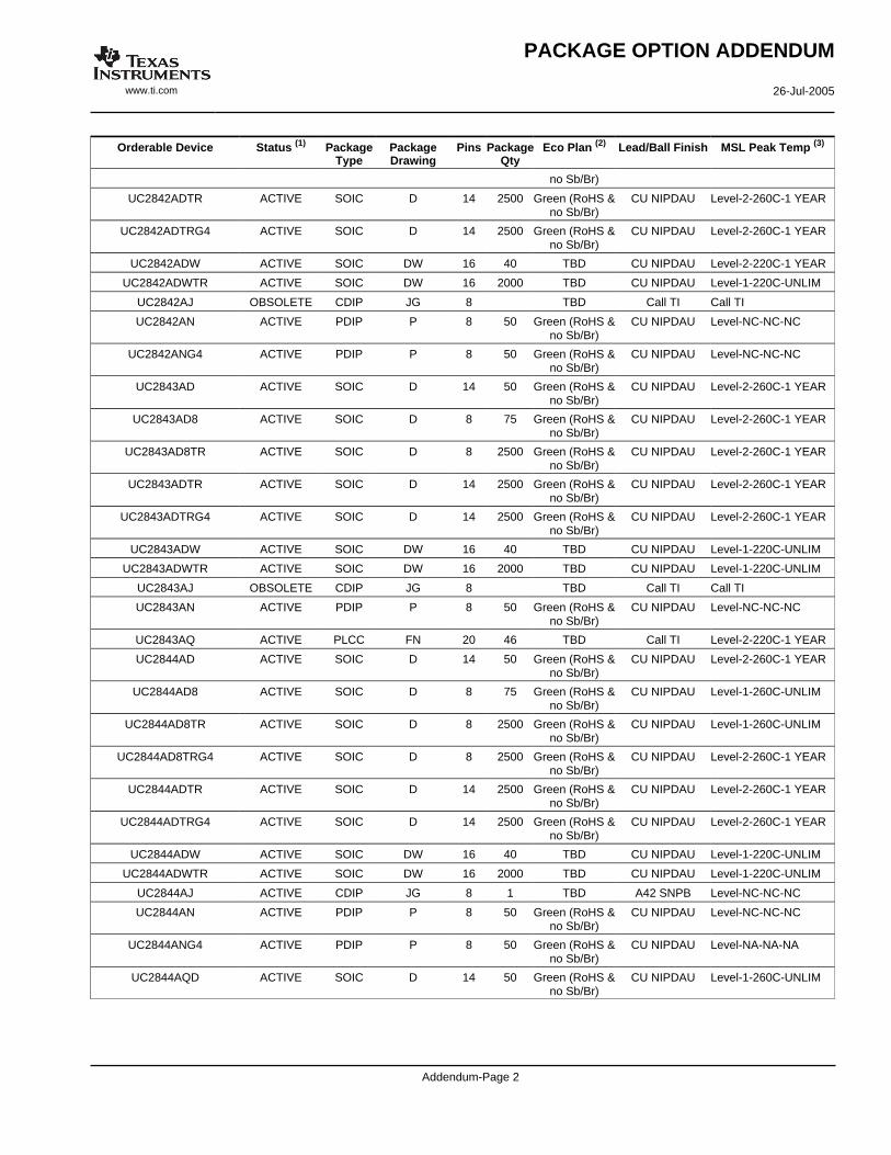
Orderable Device Status (1) PackageType
PackageDrawing
Pins PackageQty
Eco Plan (2) Lead/Ball Finish MSL Peak Temp (3)
no Sb/Br)
UC2842ADTR ACTIVE SOIC D 14 2500 Green (RoHS &no Sb/Br)
CU NIPDAU Level-2-260C-1 YEAR
UC2842ADTRG4 ACTIVE SOIC D 14 2500 Green (RoHS &no Sb/Br)
CU NIPDAU Level-2-260C-1 YEAR
UC2842ADW ACTIVE SOIC DW 16 40 TBD CU NIPDAU Level-2-220C-1 YEAR
UC2842ADWTR ACTIVE SOIC DW 16 2000 TBD CU NIPDAU Level-1-220C-UNLIM
UC2842AJ OBSOLETE CDIP JG 8 TBD Call TI Call TI
UC2842AN ACTIVE PDIP P 8 50 Green (RoHS &no Sb/Br)
CU NIPDAU Level-NC-NC-NC
UC2842ANG4 ACTIVE PDIP P 8 50 Green (RoHS &no Sb/Br)
CU NIPDAU Level-NC-NC-NC
UC2843AD ACTIVE SOIC D 14 50 Green (RoHS &no Sb/Br)
CU NIPDAU Level-2-260C-1 YEAR
UC2843AD8 ACTIVE SOIC D 8 75 Green (RoHS &no Sb/Br)
CU NIPDAU Level-2-260C-1 YEAR
UC2843AD8TR ACTIVE SOIC D 8 2500 Green (RoHS &no Sb/Br)
CU NIPDAU Level-2-260C-1 YEAR
UC2843ADTR ACTIVE SOIC D 14 2500 Green (RoHS &no Sb/Br)
CU NIPDAU Level-2-260C-1 YEAR
UC2843ADTRG4 ACTIVE SOIC D 14 2500 Green (RoHS &no Sb/Br)
CU NIPDAU Level-2-260C-1 YEAR
UC2843ADW ACTIVE SOIC DW 16 40 TBD CU NIPDAU Level-1-220C-UNLIM
UC2843ADWTR ACTIVE SOIC DW 16 2000 TBD CU NIPDAU Level-1-220C-UNLIM
UC2843AJ OBSOLETE CDIP JG 8 TBD Call TI Call TI
UC2843AN ACTIVE PDIP P 8 50 Green (RoHS &no Sb/Br)
CU NIPDAU Level-NC-NC-NC
UC2843AQ ACTIVE PLCC FN 20 46 TBD Call TI Level-2-220C-1 YEAR
UC2844AD ACTIVE SOIC D 14 50 Green (RoHS &no Sb/Br)
CU NIPDAU Level-2-260C-1 YEAR
UC2844AD8 ACTIVE SOIC D 8 75 Green (RoHS &no Sb/Br)
CU NIPDAU Level-1-260C-UNLIM
UC2844AD8TR ACTIVE SOIC D 8 2500 Green (RoHS &no Sb/Br)
CU NIPDAU Level-1-260C-UNLIM
UC2844AD8TRG4 ACTIVE SOIC D 8 2500 Green (RoHS &no Sb/Br)
CU NIPDAU Level-2-260C-1 YEAR
UC2844ADTR ACTIVE SOIC D 14 2500 Green (RoHS &no Sb/Br)
CU NIPDAU Level-2-260C-1 YEAR
UC2844ADTRG4 ACTIVE SOIC D 14 2500 Green (RoHS &no Sb/Br)
CU NIPDAU Level-2-260C-1 YEAR
UC2844ADW ACTIVE SOIC DW 16 40 TBD CU NIPDAU Level-1-220C-UNLIM
UC2844ADWTR ACTIVE SOIC DW 16 2000 TBD CU NIPDAU Level-1-220C-UNLIM
UC2844AJ ACTIVE CDIP JG 8 1 TBD A42 SNPB Level-NC-NC-NC
UC2844AN ACTIVE PDIP P 8 50 Green (RoHS &no Sb/Br)
CU NIPDAU Level-NC-NC-NC
UC2844ANG4 ACTIVE PDIP P 8 50 Green (RoHS &no Sb/Br)
CU NIPDAU Level-NA-NA-NA
UC2844AQD ACTIVE SOIC D 14 50 Green (RoHS &no Sb/Br)
CU NIPDAU Level-1-260C-UNLIM
PACKAGE OPTION ADDENDUM
www.ti.com 26-Jul-2005
Addendum-Page 2
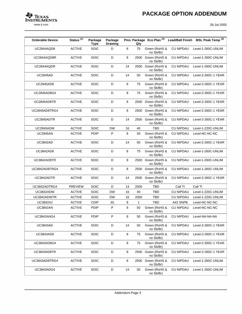
Orderable Device Status (1) PackageType
PackageDrawing
Pins PackageQty
Eco Plan (2) Lead/Ball Finish MSL Peak Temp (3)
UC2844AQD8 ACTIVE SOIC D 8 75 Green (RoHS &no Sb/Br)
CU NIPDAU Level-1-260C-UNLIM
UC2844AQD8R ACTIVE SOIC D 8 2500 Green (RoHS &no Sb/Br)
CU NIPDAU Level-1-260C-UNLIM
UC2844AQDR ACTIVE SOIC D 14 2500 Green (RoHS &no Sb/Br)
CU NIPDAU Level-1-260C-UNLIM
UC2845AD ACTIVE SOIC D 14 50 Green (RoHS &no Sb/Br)
CU NIPDAU Level-2-260C-1 YEAR
UC2845AD8 ACTIVE SOIC D 8 75 Green (RoHS &no Sb/Br)
CU NIPDAU Level-2-260C-1 YEAR
UC2845AD8G4 ACTIVE SOIC D 8 75 Green (RoHS &no Sb/Br)
CU NIPDAU Level-2-260C-1 YEAR
UC2845AD8TR ACTIVE SOIC D 8 2500 Green (RoHS &no Sb/Br)
CU NIPDAU Level-2-260C-1 YEAR
UC2845AD8TRG4 ACTIVE SOIC D 8 2500 Green (RoHS &no Sb/Br)
CU NIPDAU Level-2-260C-1 YEAR
UC2845ADTR ACTIVE SOIC D 14 2500 Green (RoHS &no Sb/Br)
CU NIPDAU Level-2-260C-1 YEAR
UC2845ADW ACTIVE SOIC DW 16 40 TBD CU NIPDAU Level-1-220C-UNLIM
UC2845AN ACTIVE PDIP P 8 50 Green (RoHS &no Sb/Br)
CU NIPDAU Level-NC-NC-NC
UC3842AD ACTIVE SOIC D 14 50 Green (RoHS &no Sb/Br)
CU NIPDAU Level-2-260C-1 YEAR
UC3842AD8 ACTIVE SOIC D 8 75 Green (RoHS &no Sb/Br)
CU NIPDAU Level-1-260C-UNLIM
UC3842AD8TR ACTIVE SOIC D 8 2500 Green (RoHS &no Sb/Br)
CU NIPDAU Level-1-260C-UNLIM
UC3842AD8TRG4 ACTIVE SOIC D 8 2500 Green (RoHS &no Sb/Br)
CU NIPDAU Level-1-260C-UNLIM
UC3842ADTR ACTIVE SOIC D 14 2500 Green (RoHS &no Sb/Br)
CU NIPDAU Level-2-260C-1 YEAR
UC3842ADTRG4 PREVIEW SOIC D 14 2000 TBD Call TI Call TI
UC3842ADW ACTIVE SOIC DW 16 40 TBD CU NIPDAU Level-1-220C-UNLIM
UC3842ADWTR ACTIVE SOIC DW 16 2000 TBD CU NIPDAU Level-1-220C-UNLIM
UC3842AJ ACTIVE CDIP JG 8 1 TBD A42 SNPB Level-NC-NC-NC
UC3842AN ACTIVE PDIP P 8 50 Green (RoHS &no Sb/Br)
CU NIPDAU Level-NC-NC-NC
UC3842ANG4 ACTIVE PDIP P 8 50 Green (RoHS &no Sb/Br)
CU NIPDAU Level-NA-NA-NA
UC3843AD ACTIVE SOIC D 14 50 Green (RoHS &no Sb/Br)
CU NIPDAU Level-2-260C-1 YEAR
UC3843AD8 ACTIVE SOIC D 8 75 Green (RoHS &no Sb/Br)
CU NIPDAU Level-2-260C-1 YEAR
UC3843AD8G4 ACTIVE SOIC D 8 75 Green (RoHS &no Sb/Br)
CU NIPDAU Level-2-260C-1 YEAR
UC3843AD8TR ACTIVE SOIC D 8 2500 Green (RoHS &no Sb/Br)
CU NIPDAU Level-2-260C-1 YEAR
UC3843AD8TRG4 ACTIVE SOIC D 8 2500 Green (RoHS &no Sb/Br)
CU NIPDAU Level-1-260C-UNLIM
UC3843ADG4 ACTIVE SOIC D 14 50 Green (RoHS &no Sb/Br)
CU NIPDAU Level-1-260C-UNLIM
PACKAGE OPTION ADDENDUM
www.ti.com 26-Jul-2005
Addendum-Page 3
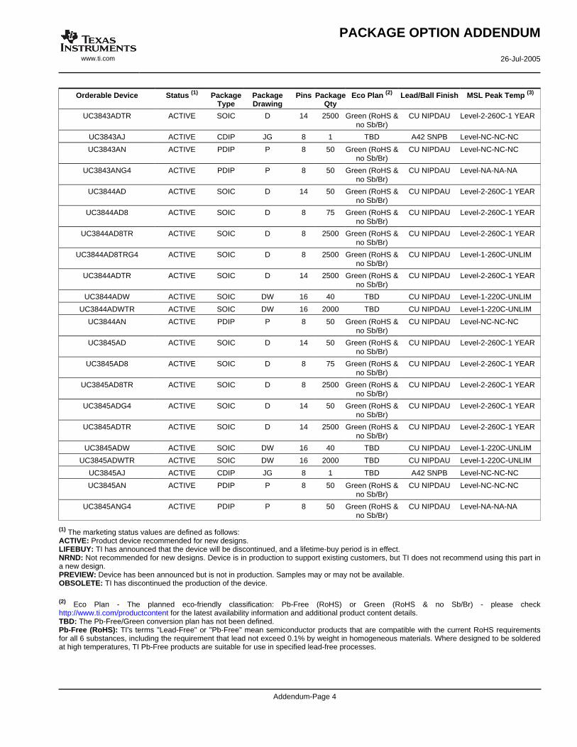
Orderable Device Status (1) PackageType
PackageDrawing
Pins PackageQty
Eco Plan (2) Lead/Ball Finish MSL Peak Temp (3)
UC3843ADTR ACTIVE SOIC D 14 2500 Green (RoHS &no Sb/Br)
CU NIPDAU Level-2-260C-1 YEAR
UC3843AJ ACTIVE CDIP JG 8 1 TBD A42 SNPB Level-NC-NC-NC
UC3843AN ACTIVE PDIP P 8 50 Green (RoHS &no Sb/Br)
CU NIPDAU Level-NC-NC-NC
UC3843ANG4 ACTIVE PDIP P 8 50 Green (RoHS &no Sb/Br)
CU NIPDAU Level-NA-NA-NA
UC3844AD ACTIVE SOIC D 14 50 Green (RoHS &no Sb/Br)
CU NIPDAU Level-2-260C-1 YEAR
UC3844AD8 ACTIVE SOIC D 8 75 Green (RoHS &no Sb/Br)
CU NIPDAU Level-2-260C-1 YEAR
UC3844AD8TR ACTIVE SOIC D 8 2500 Green (RoHS &no Sb/Br)
CU NIPDAU Level-2-260C-1 YEAR
UC3844AD8TRG4 ACTIVE SOIC D 8 2500 Green (RoHS &no Sb/Br)
CU NIPDAU Level-1-260C-UNLIM
UC3844ADTR ACTIVE SOIC D 14 2500 Green (RoHS &no Sb/Br)
CU NIPDAU Level-2-260C-1 YEAR
UC3844ADW ACTIVE SOIC DW 16 40 TBD CU NIPDAU Level-1-220C-UNLIM
UC3844ADWTR ACTIVE SOIC DW 16 2000 TBD CU NIPDAU Level-1-220C-UNLIM
UC3844AN ACTIVE PDIP P 8 50 Green (RoHS &no Sb/Br)
CU NIPDAU Level-NC-NC-NC
UC3845AD ACTIVE SOIC D 14 50 Green (RoHS &no Sb/Br)
CU NIPDAU Level-2-260C-1 YEAR
UC3845AD8 ACTIVE SOIC D 8 75 Green (RoHS &no Sb/Br)
CU NIPDAU Level-2-260C-1 YEAR
UC3845AD8TR ACTIVE SOIC D 8 2500 Green (RoHS &no Sb/Br)
CU NIPDAU Level-2-260C-1 YEAR
UC3845ADG4 ACTIVE SOIC D 14 50 Green (RoHS &no Sb/Br)
CU NIPDAU Level-2-260C-1 YEAR
UC3845ADTR ACTIVE SOIC D 14 2500 Green (RoHS &no Sb/Br)
CU NIPDAU Level-2-260C-1 YEAR
UC3845ADW ACTIVE SOIC DW 16 40 TBD CU NIPDAU Level-1-220C-UNLIM
UC3845ADWTR ACTIVE SOIC DW 16 2000 TBD CU NIPDAU Level-1-220C-UNLIM
UC3845AJ ACTIVE CDIP JG 8 1 TBD A42 SNPB Level-NC-NC-NC
UC3845AN ACTIVE PDIP P 8 50 Green (RoHS &no Sb/Br)
CU NIPDAU Level-NC-NC-NC
UC3845ANG4 ACTIVE PDIP P 8 50 Green (RoHS &no Sb/Br)
CU NIPDAU Level-NA-NA-NA
(1) The marketing status values are defined as follows:ACTIVE: Product device recommended for new designs.LIFEBUY: TI has announced that the device will be discontinued, and a lifetime-buy period is in effect.NRND: Not recommended for new designs. Device is in production to support existing customers, but TI does not recommend using this part ina new design.PREVIEW: Device has been announced but is not in production. Samples may or may not be available.OBSOLETE: TI has discontinued the production of the device.
(2) Eco Plan - The planned eco-friendly classification: Pb-Free (RoHS) or Green (RoHS & no Sb/Br) - please checkhttp://www.ti.com/productcontent for the latest availability information and additional product content details.TBD: The Pb-Free/Green conversion plan has not been defined.Pb-Free (RoHS): TI's terms "Lead-Free" or "Pb-Free" mean semiconductor products that are compatible with the current RoHS requirementsfor all 6 substances, including the requirement that lead not exceed 0.1% by weight in homogeneous materials. Where designed to be solderedat high temperatures, TI Pb-Free products are suitable for use in specified lead-free processes.
PACKAGE OPTION ADDENDUM
www.ti.com 26-Jul-2005
Addendum-Page 4
Green (RoHS & no Sb/Br): TI defines "Green" to mean Pb-Free (RoHS compatible), and free of Bromine (Br) and Antimony (Sb) based flameretardants (Br or Sb do not exceed 0.1% by weight in homogeneous material)
(3) MSL, Peak Temp. -- The Moisture Sensitivity Level rating according to the JEDEC industry standard classifications, and peak soldertemperature.
Important Information and Disclaimer:The information provided on this page represents TI's knowledge and belief as of the date that it isprovided. TI bases its knowledge and belief on information provided by third parties, and makes no representation or warranty as to theaccuracy of such information. Efforts are underway to better integrate information from third parties. TI has taken and continues to takereasonable steps to provide representative and accurate information but may not have conducted destructive testing or chemical analysis onincoming materials and chemicals. TI and TI suppliers consider certain information to be proprietary, and thus CAS numbers and other limitedinformation may not be available for release.
In no event shall TI's liability arising out of such information exceed the total purchase price of the TI part(s) at issue in this document sold by TIto Customer on an annual basis.
PACKAGE OPTION ADDENDUM
www.ti.com 26-Jul-2005
Addendum-Page 5
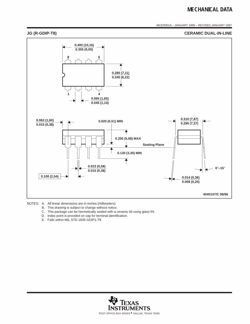
MECHANICAL DATA
MCER001A – JANUARY 1995 – REVISED JANUARY 1997
POST OFFICE BOX 655303 • DALLAS, TEXAS 75265
JG (R-GDIP-T8) CERAMIC DUAL-IN-LINE
0.310 (7,87)0.290 (7,37)
0.014 (0,36)0.008 (0,20)
Seating Plane
4040107/C 08/96
5
40.065 (1,65)0.045 (1,14)
8
1
0.020 (0,51) MIN
0.400 (10,16)0.355 (9,00)
0.015 (0,38)0.023 (0,58)
0.063 (1,60)0.015 (0,38)
0.200 (5,08) MAX
0.130 (3,30) MIN
0.245 (6,22)0.280 (7,11)
0.100 (2,54)
0°–15°
NOTES: A. All linear dimensions are in inches (millimeters).B. This drawing is subject to change without notice.C. This package can be hermetically sealed with a ceramic lid using glass frit.D. Index point is provided on cap for terminal identification.E. Falls within MIL STD 1835 GDIP1-T8
MECHANICAL DATA
MLCC006B – OCTOBER 1996
POST OFFICE BOX 655303 • DALLAS, TEXAS 75265
FK (S-CQCC-N**) LEADLESS CERAMIC CHIP CARRIER
4040140/D 10/96
28 TERMINAL SHOWN
B
0.358(9,09)
MAX
(11,63)
0.560(14,22)
0.560
0.458
0.858(21,8)
1.063(27,0)
(14,22)
ANO. OF
MINMAX
0.358
0.660
0.761
0.458
0.342(8,69)
MIN
(11,23)
(16,26)0.640
0.739
0.442
(9,09)
(11,63)
(16,76)
0.962
1.165
(23,83)0.938
(28,99)1.141
(24,43)
(29,59)
(19,32)(18,78)
**
20
28
52
44
68
84
0.020 (0,51)
TERMINALS
0.080 (2,03)0.064 (1,63)
(7,80)0.307
(10,31)0.406
(12,58)0.495
(12,58)0.495
(21,6)0.850
(26,6)1.047
0.045 (1,14)
0.045 (1,14)0.035 (0,89)
0.035 (0,89)
0.010 (0,25)
121314151618 17
11
10
8
9
7
5
432
0.020 (0,51)0.010 (0,25)
6
12826 27
19
21B SQ
A SQ22
23
24
25
20
0.055 (1,40)0.045 (1,14)
0.028 (0,71)0.022 (0,54)
0.050 (1,27)
NOTES: A. All linear dimensions are in inches (millimeters).B. This drawing is subject to change without notice.C. This package can be hermetically sealed with a metal lid.D. The terminals are gold plated.E. Falls within JEDEC MS-004
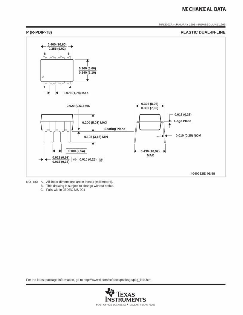
MECHANICAL DATA
MPDI001A – JANUARY 1995 – REVISED JUNE 1999
POST OFFICE BOX 655303 • DALLAS, TEXAS 75265
P (R-PDIP-T8) PLASTIC DUAL-IN-LINE
8
4
0.015 (0,38)
Gage Plane
0.325 (8,26)0.300 (7,62)
0.010 (0,25) NOM
MAX0.430 (10,92)
4040082/D 05/98
0.200 (5,08) MAX
0.125 (3,18) MIN
5
0.355 (9,02)
0.020 (0,51) MIN
0.070 (1,78) MAX
0.240 (6,10)0.260 (6,60)
0.400 (10,60)
1
0.015 (0,38)0.021 (0,53)
Seating Plane
M0.010 (0,25)
0.100 (2,54)
NOTES: A. All linear dimensions are in inches (millimeters).B. This drawing is subject to change without notice.C. Falls within JEDEC MS-001
For the latest package information, go to http://www.ti.com/sc/docs/package/pkg_info.htm
MECHANICAL DATA
MPLC004A – OCTOBER 1994
POST OFFICE BOX 655303 • DALLAS, TEXAS 75265
FN (S-PQCC-J**) PLASTIC J-LEADED CHIP CARRIER
4040005/B 03/95
20 PIN SHOWN
0.026 (0,66)0.032 (0,81)
D2/E2
0.020 (0,51) MIN
0.180 (4,57) MAX0.120 (3,05)0.090 (2,29)
D2/E2
0.013 (0,33)0.021 (0,53)
Seating Plane
MAX
D2/E2
0.219 (5,56)
0.169 (4,29)
0.319 (8,10)
0.469 (11,91)
0.569 (14,45)
0.369 (9,37)
MAX
0.356 (9,04)
0.456 (11,58)
0.656 (16,66)
0.008 (0,20) NOM
1.158 (29,41)
0.958 (24,33)
0.756 (19,20)
0.191 (4,85)
0.141 (3,58)
MIN
0.441 (11,20)
0.541 (13,74)
0.291 (7,39)
0.341 (8,66)
18
19
14
13
D
D1
13
9
E1E
4
8
MINMAXMINPINS
**
20
28
44
0.385 (9,78)
0.485 (12,32)
0.685 (17,40)
52
68
84 1.185 (30,10)
0.985 (25,02)
0.785 (19,94)
D/E
0.395 (10,03)
0.495 (12,57)
1.195 (30,35)
0.995 (25,27)
0.695 (17,65)
0.795 (20,19)
NO. OF D1/E1
0.350 (8,89)
0.450 (11,43)
1.150 (29,21)
0.950 (24,13)
0.650 (16,51)
0.750 (19,05)
0.004 (0,10)
M0.007 (0,18)
0.050 (1,27)
NOTES: A. All linear dimensions are in inches (millimeters).B. This drawing is subject to change without notice.C. Falls within JEDEC MS-018
IMPORTANT NOTICE
Texas Instruments Incorporated and its subsidiaries (TI) reserve the right to make corrections, modifications,enhancements, improvements, and other changes to its products and services at any time and to discontinueany product or service without notice. Customers should obtain the latest relevant information before placingorders and should verify that such information is current and complete. All products are sold subject to TI’s termsand conditions of sale supplied at the time of order acknowledgment.
TI warrants performance of its hardware products to the specifications applicable at the time of sale inaccordance with TI’s standard warranty. Testing and other quality control techniques are used to the extent TIdeems necessary to support this warranty. Except where mandated by government requirements, testing of allparameters of each product is not necessarily performed.
TI assumes no liability for applications assistance or customer product design. Customers are responsible fortheir products and applications using TI components. To minimize the risks associated with customer productsand applications, customers should provide adequate design and operating safeguards.
TI does not warrant or represent that any license, either express or implied, is granted under any TI patent right,copyright, mask work right, or other TI intellectual property right relating to any combination, machine, or processin which TI products or services are used. Information published by TI regarding third-party products or servicesdoes not constitute a license from TI to use such products or services or a warranty or endorsement thereof.Use of such information may require a license from a third party under the patents or other intellectual propertyof the third party, or a license from TI under the patents or other intellectual property of TI.
Reproduction of information in TI data books or data sheets is permissible only if reproduction is withoutalteration and is accompanied by all associated warranties, conditions, limitations, and notices. Reproductionof this information with alteration is an unfair and deceptive business practice. TI is not responsible or liable forsuch altered documentation.
Resale of TI products or services with statements different from or beyond the parameters stated by TI for thatproduct or service voids all express and any implied warranties for the associated TI product or service andis an unfair and deceptive business practice. TI is not responsible or liable for any such statements.
Following are URLs where you can obtain information on other Texas Instruments products and applicationsolutions:
Products Applications
Amplifiers amplifier.ti.com Audio www.ti.com/audio
Data Converters dataconverter.ti.com Automotive www.ti.com/automotive
DSP dsp.ti.com Broadband www.ti.com/broadband
Interface interface.ti.com Digital Control www.ti.com/digitalcontrol
Logic logic.ti.com Military www.ti.com/military
Power Mgmt power.ti.com Optical Networking www.ti.com/opticalnetwork
Microcontrollers microcontroller.ti.com Security www.ti.com/security
Telephony www.ti.com/telephony
Video & Imaging www.ti.com/video
Wireless www.ti.com/wireless
Mailing Address: Texas Instruments
Post Office Box 655303 Dallas, Texas 75265
Copyright 2005, Texas Instruments Incorporated


![[ applicaTion noTe ] - · PDF fileBisphenol A is used in the production of epoxy resins and polycar- ... [applicaTion noTe] Waters Corporation 34 Maple Street Milford, MA 01757 U.S.A](https://img.pdfslide.us/doc/110x75/5a76e9947f8b9a93088d7aec/-application-note-waters-a-bisphenol-a-is-used-in-the-production-of-epoxy.jpg)