Embed Size (px)
Citation preview
Celeritous Technical Services Corp 800.687.6510 / 806.793.0708 3308 34th St FAX 806.793.0710 Lubbock, Texas 79410 http://www.celeritous.com
SPECIFICATIONS SUBJECT TO CHANGE WITHOUT NOTICE
Copyright 2000 Celeritous Technical Services Corp 1 Rev E Tuesday, September 25,
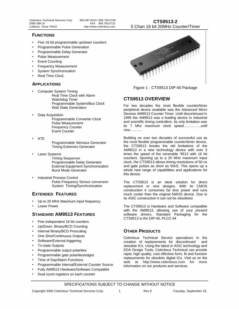
CTS9513-2 5 Chan 16 bit 20MHz Counter/Timer
FUNCTIONS • Five 16 bit programmable up/down counters • Programmable Pulse Generation • Programmable Delay Generator • Pulse Measurement • Event Counting • Frequency Measurement • System Synchronization • Real Time Clock
APPLICATIONS • Computer System Timing
Real Time Clock with Alarm Watchdog Timer Programmable System/Bus Clock Wait State Generation
• Data Acquisition Programmable Converter Clock Pulse Measurement Frequency Counter Event Counter
• ATE Programmable Stimulus Generator Timing Extremes Generator
• Laser Systems Timing Sequencer Programmable Delay Generator External Equipment Synchronization Burst Mode Generator
• Industrial Process Control Pulse Frequency Sensor conversion System Timing/Synchronization
EXTENDED FEATURES • Up to 20 MHz Maximum input frequency • Lower Power
STANDARD AM9513 FEATURES • Five independent 16 bit counters • Up/Down, Binary/BCD Counting • Internal Binary/BCD Prescaling • One Shot/Continuous Outputs • Software/External triggering • Tri-state Outputs • Programmable output polarities • Programmable gate polarities/edges • Time of Day/Alarm Functions • Programmable Internal/External Counter Source • Fully AM9513 Hardware/Software Compatible • Dual count registers on each counter
CTS9513 OVERVIEW For two decades the most flexible counter/timer peripheral device available was the Advanced Micro Devices AM9513 Counter Timer. Until discontinued in 1995 the AM9513 was a leading device in industrial and scientific timing controllers. Its only limitation was its 7 Mhz maximum clock speed…….……..until now............ Building on over two decades of successful use as the most flexible programmable counter/timer device, the CTS9513 breaks the old limitations of the AM9513 in a new technology device with over 3 times the speed of the venerable ‘9513 with 16 bit counters. Sporting up to a 20 MHz maximum Input clock, the CTS9513 allows timing resolutions of 50 ns and gate pulses as short as 50nS. This opens up a whole new range of capabilities and applications for this device. The CTS9513 is an ideal solution for direct replacement or new designs. With its CMOS construction it consumes far less power and runs much cooler than the original NMOS device. Due to its ASIC construction it can not be obsoleted The CTS9513 is Hardware and Software compatible with the AM9513, allowing use of your present software drivers. Standard Packaging for the CTS9513 is the DIP-40, PLCC-44
OTHER PRODUCTS Celeritous Technical Service specializes in the creation of replacements for discontinued and obsolete ICs. Using the latest in ASIC technology and EDA Design Tools, Celeritous Technical can provide rapid, high quality, cost effective form, fit and function replacements for obsolete digital ICs. Visit us on the web at http://www.celeritous.com for more information on our products and services.
Figure 1 - CTS9513 DIP-40 Package
Celeritous Technical Services Corp 800.687.6510 / 806.793.0708 3308 34th St FAX 806.793.0710 Lubbock, Texas 79410 http://www.celeritous.com
SPECIFICATIONS SUBJECT TO CHANGE WITHOUT NOTICE
Copyright 2000 Celeritous Technical Services Corp 2 Rev E Tuesday, September 25,
CTS9513-2 5 Chan 16 bit 20MHz Counter/Timer
DEVICE DESCRIPTION The CTS9513 is a custom, high speed ASIC implementation of the AMD AM9513 System Timing Controller. The ‘9513 has long been the most versatile counter/timer peripheral device, featuring far more flexibility than competing timing devices such as the Intel 8253/8254, Motorola 6840 or others. A large installed base of devices and software drivers already exists. The principal limitation of the AM9513 was its maximum frequency limitation of 7 Mhz imposed by its late 1970’s NMOS LSI design. The CTS9513 shatters this barrier with a 20 MHz maximum clock speed and much lower power consumption due to its CMOS construction. The CTS9513 Counter/Timer is capable of a wide variety of applications including, but not limited to:
• Event Counting • Event Sequencing • Programmable pulse generation • Programmable delay generation • Frequency counting • Frequency synthesis • Real Time Clock • Alarm Clock Functions • Watchdog Timing • Retriggerable Pulse Generation • Non-Retriggerable Pulse Generation • Waveform Analysis • Interrupt Generation • Pulse burst generation The user has control over key features such as:
• Output Polarities • Output Impedance • Input Trigger, Edge Polarities • Hardware gating/triggering • Software gating/triggering • Count Up/Down • BCD/Binary Counting • Real time count register read • Internal counter concatenation (up to 80 bits) • Programmable frequency source selection • Programmable internal clock pre-scaling
FEATURES
BACKWARDS COMPATIBLE The CTS9513 maintains backwards compatibility with most AM9513 features, allowing continued use of your existing software drivers. Data may be transferred in 8 or 16 bit increments. All internal data paths in the CTS9513 are 16 bit. All ‘9513 commands registers and modes are supported.
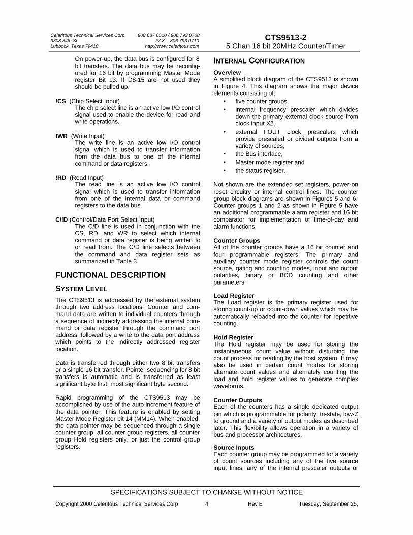
PACKAGING Figure 2 illustrates the DIP-40 Package pinout of the device which conforms to the original AM9513 pinouts. Table 2 summarizes the pinouts of the PLCC-44 package illustrated in Figure 3 which conform to the original AM9513 PLCC pinouts. SIGNALS The following signal names and description conform to the original AM9513 device. VCC
+5 Volt Power Supply
VSS Ground
X1
The CTS9513 does not provide an internal crystal oscillator and must be driven from an external source. X1 should be left open
X2 X2 should be connected to an external TTL source and pulled up to VCC
FOUT (Frequency Divider Outputs)
The FOUT line is generated by internally programmable counters. The clock source for these counters may be any of the external GATE or SOURCE inputs as well as any of the internally prescaled clock outputs.
SOURCE1-5 (Count Source Inputs)
Source inputs 1-5 provide external clock source lines which may be routed to any of the internal counters or the FOUT divider. The active count edge for the source is programmed at the counter.
Symbol Description Min Max Units
V DD DC Supply Voltage -0.3 7 Volts
V IN Input Voltage at Any Pin -0.3 VDD+.3 Volts
T OP Operating Temperature AxI -40 85 o C
T ST Storage Temperature -55 150 o C
Table 1. Absolute Maximum Ratings
Celeritous Technical Services Corp 800.687.6510 / 806.793.0708 3308 34th St FAX 806.793.0710 Lubbock, Texas 79410 http://www.celeritous.com
SPECIFICATIONS SUBJECT TO CHANGE WITHOUT NOTICE
Copyright 2000 Celeritous Technical Services Corp 3 Rev E Tuesday, September 25,
CTS9513-2 5 Chan 16 bit 20MHz Counter/Timer
2
1
3
4
5
6
7
8
9
10
11
12
13
14
15
16
17
18
19
20
40
39
38
37
36
35
34
33
32
31
30
29
28
27
26
25
24
23
22
21
VCC
OUT 2
OUT 1
GATE 1
X 1
X 2
FOUT
C/D
RD
D0
D1
D2
D3
D4
D5
D6
WR
CS
D7
GATE 1A / D8
OUT 3
GATE 2
OUT 4
OUT 5
GATE 3
GATE 4
GATE 5
SOURCE 1
SOURCE 2
SOURCE 3
SOURCE 4
SOURCE 5
D 15
D 14
D 13
GATE 5A / D12
GATE 4A / D11
GATE 3A / D10
GATE 2A / D9
VSS
Figure 2 - CTS9513 DIP-40 Package Pinouts
Table 2 - CTS9513 Ordering Information
CTSC9513A x x - x
Package
Plastic DIP-40 P
Plastic PLCC-44 J
Temperature Range
Industrial (-40 - 85º C) I
Maximum Clock Speed
20 MHz 2
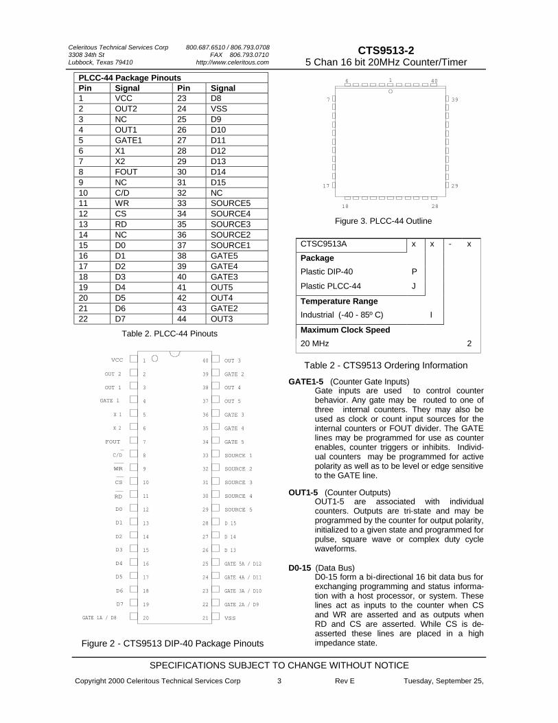
Pin Signal Pin Signal 1 VCC 23 D8 2 OUT2 24 VSS 3 NC 25 D9 4 OUT1 26 D10 5 GATE1 27 D11 6 X1 28 D12 7 X2 29 D13 8 FOUT 30 D14 9 NC 31 D15 10 C/D 32 NC 11 WR 33 SOURCE5 12 CS 34 SOURCE4 13 RD 35 SOURCE3 14 NC 36 SOURCE2 15 D0 37 SOURCE1 16 D1 38 GATE5 17 D2 39 GATE4 18 D3 40 GATE3 19 D4 41 OUT5 20 D5 42 OUT4 21 D6 43 GATE2 22 D7 44 OUT3
PLCC-44 Package Pinouts
Table 2. PLCC-44 Pinouts
Figure 3. PLCC-44 Outline
GATE1-5 (Counter Gate Inputs) Gate inputs are used to control counter behavior. Any gate may be routed to one of three internal counters. They may also be used as clock or count input sources for the internal counters or FOUT divider. The GATE lines may be programmed for use as counter enables, counter triggers or inhibits. Individ-ual counters may be programmed for active polarity as well as to be level or edge sensitive to the GATE line.
OUT1-5 (Counter Outputs) OUT1-5 are associated with individual counters. Outputs are tri-state and may be programmed by the counter for output polarity, initialized to a given state and programmed for pulse, square wave or complex duty cycle waveforms.
D0-15 (Data Bus) D0-15 form a bi-directional 16 bit data bus for exchanging programming and status informa-tion with a host processor, or system. These lines act as inputs to the counter when CS and WR are asserted and as outputs when RD and CS are asserted. While CS is de-asserted these lines are placed in a high impedance state.
16
7
17
18 28
29
39
40
Celeritous Technical Services Corp 800.687.6510 / 806.793.0708 3308 34th St FAX 806.793.0710 Lubbock, Texas 79410 http://www.celeritous.com
SPECIFICATIONS SUBJECT TO CHANGE WITHOUT NOTICE
Copyright 2000 Celeritous Technical Services Corp 4 Rev E Tuesday, September 25,
CTS9513-2 5 Chan 16 bit 20MHz Counter/Timer
On power-up, the data bus is configured for 8 bit transfers. The data bus may be reconfig-ured for 16 bit by programming Master Mode register Bit 13. If D8-15 are not used they should be pulled up.
!CS (Chip Select Input) The chip select line is an active low I/O control signal used to enable the device for read and write operations.
!WR (Write Input) The write line is an active low I/O control signal which is used to transfer information from the data bus to one of the internal command or data registers.
!RD (Read Input)
The read line is an active low I/O control signal which is used to transfer information from one of the internal data or command registers to the data bus.
C/!D (Control/Data Port Select Input) The C/D line is used in conjunction with the CS, RD, and WR to select which internal command or data register is being written to or read from. The C/D line selects between the command and data register sets as summarized in Table 3
FUNCTIONAL DESCRIPTION
SYSTEM LEVEL The CTS9513 is addressed by the external system through two address locations. Counter and com-mand data are written to individual counters through a sequence of indirectly addressing the internal com-mand or data register through the command port address, followed by a write to the data port address which points to the indirectly addressed register location. Data is transferred through either two 8 bit transfers or a single 16 bit transfer. Pointer sequencing for 8 bit transfers is automatic and is transferred as least significant byte first, most significant byte second. Rapid programming of the CTS9513 may be accomplished by use of the auto-increment feature of the data pointer. This feature is enabled by setting Master Mode Register bit 14 (MM14). When enabled, the data pointer may be sequenced through a single counter group, all counter group registers, all counter group Hold registers only, or just the control group registers.
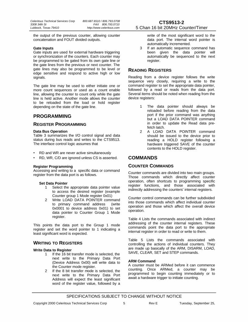
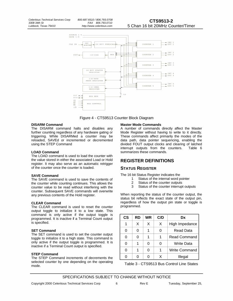
INTERNAL CONFIGURATION Overview A simplified block diagram of the CTS9513 is shown in Figure 4. This diagram shows the major device elements consisting of:
• five counter groups, • internal frequency prescaler which divides
down the primary external clock source from clock input X2,
• external FOUT clock prescalers which provide prescaled or divided outputs from a variety of sources,
• the Bus interface, • Master mode register and • the status register.
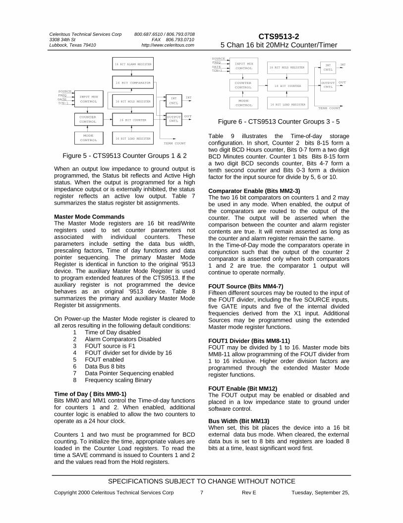
Not shown are the extended set registers, power-on reset circuitry or internal control lines. The counter group block diagrams are shown in Figures 5 and 6. Counter groups 1 and 2 as shown in Figure 5 have an additional programmable alarm register and 16 bit comparator for implementation of time-of-day and alarm functions. Counter Groups All of the counter groups have a 16 bit counter and four programmable registers. The primary and auxiliary counter mode register controls the count source, gating and counting modes, input and output polarities, binary or BCD counting and other parameters. Load Register The Load register is the primary register used for storing count-up or count-down values which may be automatically reloaded into the counter for repetitive counting. Hold Register The Hold register may be used for storing the instantaneous count value without disturbing the count process for reading by the host system. It may also be used in certain count modes for storing alternate count values and alternately counting the load and hold register values to generate complex waveforms. Counter Outputs Each of the counters has a single dedicated output pin which is programmable for polarity, tri-state, low-Z to ground and a variety of output modes as described later. This flexibility allows operation in a variety of bus and processor architectures. Source Inputs Each counter group may be programmed for a variety of count sources including any of the five source input lines, any of the internal prescaler outputs or
Celeritous Technical Services Corp 800.687.6510 / 806.793.0708 3308 34th St FAX 806.793.0710 Lubbock, Texas 79410 http://www.celeritous.com
SPECIFICATIONS SUBJECT TO CHANGE WITHOUT NOTICE
Copyright 2000 Celeritous Technical Services Corp 5 Rev E Tuesday, September 25,
CTS9513-2 5 Chan 16 bit 20MHz Counter/Timer
the output of the previous counter, allowing counter concatenation and FOUT divided outputs. Gate Inputs Gate inputs are used for external hardware triggering or synchronization of the counters. Each counter may be programmed to be gated from its own gate line or the gate lines from the previous or next counter. The gate lines may also be programmed to be level or edge sensitive and respond to active high or low signals. The gate line may be used to either initiate one or more count sequences or used as a count enable line, allowing the counter to count only while the gate line is held active. Another mode allows the counter to be reloaded from the load or hold register depending on the state of the gate line. PROGRAMMING
REGISTER PROGRAMMING Data Bus Operation Table 3 summarizes the I/O control signal and data status during bus reads and writes to the CTS9513. The interface control logic assumes that • RD and WR are never active simultaneously • RD, WR, C/D are ignored unless CS is asserted. Register Programming Accessing and writing to a specific data or command register from the data port is as follows. Set Data Pointer
1 Select the appropriate data pointer value to access the desired register (example Counter group 1 Mode register 0x01)
2 Write LOAD DATA POINTER command to primary command address (write 0x0001 to device address 0x01) to set data pointer to Counter Group 1 Mode register.
This points the data port to the Group 1 mode register and set the word pointer to 1 indicating a least significant word is expected. WRITING TO REGISTERS Write Data to Register
1 If the 16 bit transfer mode is selected, the next write to the Primary Data Port (Device Address 0x00) will write data to the Counter mode register.
2 If the 8 bit transfer mode is selected, the next write to the Primary Data Port Address will expect the least significant word of the register value, followed by a
write of the most significant word to the data port. The internal word pointer is automatically incremented.
3 If an automatic sequence command has been given the data pointer will automatically be sequenced to the next register.
READING REGISTERS Reading from a device register follows the write sequence very closely, requiring a write to the command register to set the appropriate data pointer, followed by a read or reads from the data port. Several items should be noted when reading from the device registers:
1 The data pointer should always be reloaded before reading from the data port if the prior command was anything but a LOAD DATA POINTER command in order to update the Read data pre-fetch latch.
2 A LOAD DATA POINTER command should be issued to the device prior to reading a HOLD register following a hardware triggered SAVE of the counter contents to the HOLD register.
COMMANDS
COUNTER COMMANDS Counter commands are divided into two main groups. Those commands which directly affect counter operation, often shortcuts to programming specific register functions, and those associated with indirectly addressing the counters’ internal registers. Counter control commands can be further subdivided into those commands which affect individual counter operation and those which affect the overall device operation. Table 4 Lists the commands associated with indirect addressing of the counter internal registers. These commands point the data port to the appropriate internal register in order to read or write to them. Table 5 Lists the commands associated with controlling the actions of individual counters. They are made up basically of the ARM, DISARM, LOAD, SAVE, CLEAR, SET and STEP commands. ARM Command A counter must be ARMed before it can commence counting. Once ARMed, a counter may be programmed to begin counting immediately or to await a hardware trigger to initiate counting.
Celeritous Technical Services Corp 800.687.6510 / 806.793.0708 3308 34th St FAX 806.793.0710 Lubbock, Texas 79410 http://www.celeritous.com
SPECIFICATIONS SUBJECT TO CHANGE WITHOUT NOTICE
Copyright 2000 Celeritous Technical Services Corp 6 Rev E Tuesday, September 25,
CTS9513-2 5 Chan 16 bit 20MHz Counter/Timer
Figure 4 - CTS9513 Counter Block Diagram
DISARM Command The DISARM command halts and disables any further counting regardless of any hardware gating or triggering. While DISARMed a counter may be reloaded, SAVEd or incremented or decremented using the STEP Command LOAD Command The LOAD command is used to load the counter with the value stored in either the associated Load or Hold register. It may also serve as an automatic retrigger of the counter once the counter is loaded. SAVE Command The SAVE command is used to save the contents of the counter while counting continues. This allows the counter value to be read without interfering with the counter. Subsequent SAVE commands will overwrite any previous contents of the Hold register. CLEAR Command The CLEAR command is used to reset the counter output toggle to initialize it to a low state. This command is only active if the output toggle is programmed. It is inactive if a Terminal Count output is specified. SET Command The SET command is used to set the counter output toggle to initialize it to a high state. This command is only active if the output toggle is programmed. It is inactive if a Terminal Count output is specified. STEP Command The STEP Command increments of decrements the selected counter by one depending on the operating mode.
Master Mode Commands A number of commands directly affect the Master Mode Register without having to write to it directly. These commands affect primarily the modes of the data path, data pointer sequencing, enabling the divided FOUT output clocks and clearing of latched interrupt outputs from the counters. Table 6 summarizes these commands. REGISTER DEFINITIONS
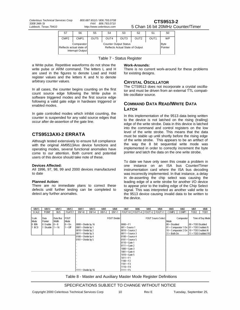
STATUS REGISTER The 16 bit Status Register indicates the
1 Status of the internal word pointer 2 Status of the counter outputs 3 Status of the counter interrupt outputs
When reporting the status of the counter output, the status bit reflects the exact state of the output pin, regardless of how the output pin state or toggle is programmed.
Table 3 - CTS9513 Bus Control Line States
CS RD WR C/D Dx
1 X X X High Impedance
0 0 1 0 Read Data
0 0 1 1 Read Command
0 1 0 0 Write Data
0 1 0 1 Write Command
0 0 0 X Illegal
COUNTER 1
COUNTER 2
COUNTER 3
COUNTER 4
COUNTER 5
SOURCE 1-5GATE 1-5
INT 1OUT 1
INT 2OUT 2
INT 3OUT 3
INT 4OUT 4
INT 5OUT 5
OSC
MUXFOUT
CLK IN
REGISTER
16 BIT MASTERMODE REGISTER
BUFFER
D0-D7D8-D15
BUS MUX
16 BIT COMMANDREGISTER
BUS CONTROL
CSRDWR
8 BIT DIVIDER
16 BIT STATUS
24 BIT PRESCALER
16 bit
C/D
Celeritous Technical Services Corp 800.687.6510 / 806.793.0708 3308 34th St FAX 806.793.0710 Lubbock, Texas 79410 http://www.celeritous.com
SPECIFICATIONS SUBJECT TO CHANGE WITHOUT NOTICE
Copyright 2000 Celeritous Technical Services Corp 7 Rev E Tuesday, September 25,
CTS9513-2 5 Chan 16 bit 20MHz Counter/Timer
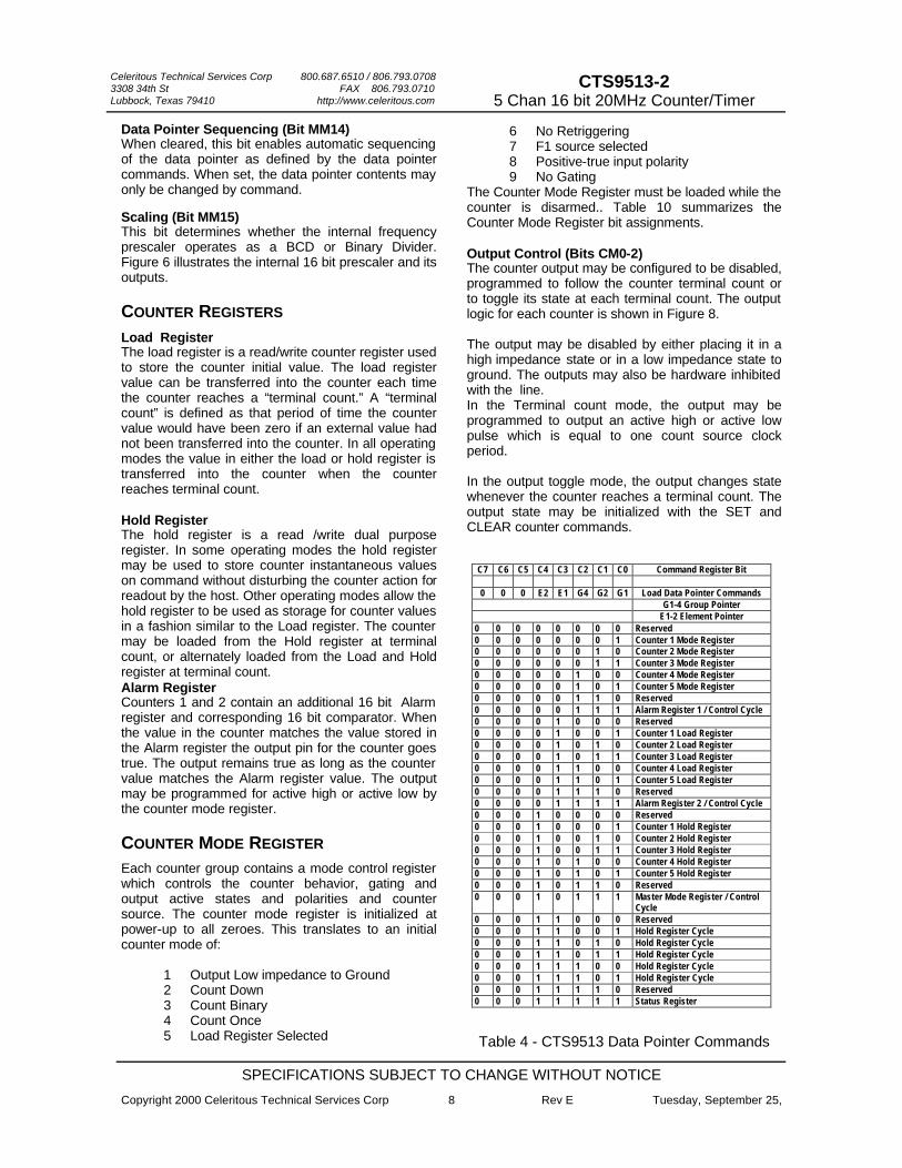
Figure 6 - CTS9513 Counter Groups 3 - 5
When an output low impedance to ground output is programmed, the Status bit reflects and Active High status. When the output is programmed for a high impedance output or is externally inhibited, the status register reflects an active low output. Table 7 summarizes the status register bit assignments. Master Mode Commands The Master Mode registers are 16 bit read/Write registers used to set counter parameters not associated with individual counters. These parameters include setting the data bus width, prescaling factors, Time of day functions and data pointer sequencing. The primary Master Mode Register is identical in function to the original ‘9513 device. The auxiliary Master Mode Register is used to program extended features of the CTS9513. If the auxiliary register is not programmed the device behaves as an original ‘9513 device. Table 8 summarizes the primary and auxiliary Master Mode Register bit assignments. On Power-up the Master Mode register is cleared to all zeros resulting in the following default conditions:
1 Time of Day disabled 2 Alarm Comparators Disabled 3 FOUT source is F1 4 FOUT divider set for divide by 16 5 FOUT enabled 6 Data Bus 8 bits 7 Data Pointer Sequencing enabled 8 Frequency scaling Binary
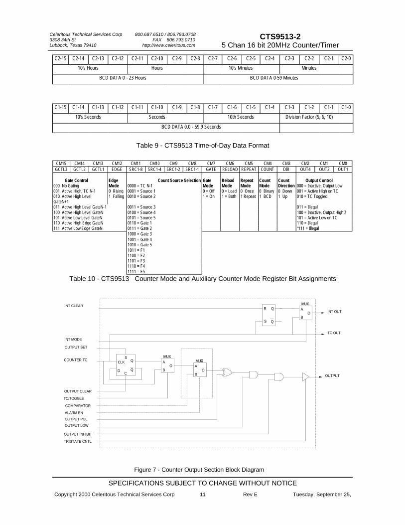
Time of Day ( Bits MM0-1) Bits MM0 and MM1 control the Time-of-day functions for counters 1 and 2. When enabled, additional counter logic is enabled to allow the two counters to operate as a 24 hour clock. Counters 1 and two must be programmed for BCD counting. To initialize the time, appropriate values are loaded in the Counter Load registers. To read the time a SAVE command is issued to Counters 1 and 2 and the values read from the Hold registers.
Table 9 illustrates the Time-of-day storage configuration. In short, Counter 2 bits 8-15 form a two digit BCD Hours counter, Bits 0-7 form a two digit BCD Minutes counter. Counter 1 bits Bits 8-15 form a two digit BCD seconds counter, Bits 4-7 form a tenth second counter and Bits 0-3 form a division factor for the input source for divide by 5, 6 or 10. Comparator Enable (Bits MM2-3) The two 16 bit comparators on counters 1 and 2 may be used in any mode. When enabled, the output of the comparators are routed to the output of the counter. The output will be asserted when the comparison between the counter and alarm register contents are true. It will remain asserted as long as the counter and alarm register remain the same. In the Time-of-Day mode the comparators operate in conjunction such that the output of the counter 2 comparator is asserted only when both comparators 1 and 2 are true. the comparator 1 output will continue to operate normally. FOUT Source (Bits MM4-7) Fifteen different sources may be routed to the input of the FOUT divider, including the five SOURCE inputs, five GATE inputs and five of the internal divided frequencies derived from the X1 input. Additional Sources may be programmed using the extended Master mode register functions. FOUT1 Divider (Bits MM8-11) FOUT may be divided by 1 to 16. Master mode bits MM8-11 allow programming of the FOUT divider from 1 to 16 inclusive. Higher order division factors are programmed through the extended Master Mode register functions. FOUT Enable (Bit MM12) The FOUT output may be enabled or disabled and placed in a low impedance state to ground under software control.
Bus Width (Bit MM13) When set, this bit places the device into a 16 bit external data bus mode. When cleared, the external data bus is set to 8 bits and registers are loaded 8 bits at a time, least significant word first.
Figure 5 - CTS9513 Counter Groups 1 & 2
16 BIT COMPARATOR
16 BIT ALARM REGISTER
16 BIT HOLD REGISTER
16 BIT COUNTER
16 BIT LOAD REGISTERTERM COUNT
OUTPUTCNTL
OUT
INTINTCNTL
INPUT MUXCONTROL
COUNTERCONTROL
MODECONTROL
SOURCEFREQGATETCN-1
16 BIT HOLD REGISTER
16 BIT COUNTER
16 BIT LOAD REGISTERTERM COUNT
OUTPUTCNTL
OUT
INTINTCNTL
INPUT MUXCONTROL
COUNTERCONTROL
MODECONTROL
SOURCEFREQGATETCN-1
Celeritous Technical Services Corp 800.687.6510 / 806.793.0708 3308 34th St FAX 806.793.0710 Lubbock, Texas 79410 http://www.celeritous.com
SPECIFICATIONS SUBJECT TO CHANGE WITHOUT NOTICE
Copyright 2000 Celeritous Technical Services Corp 8 Rev E Tuesday, September 25,
CTS9513-2 5 Chan 16 bit 20MHz Counter/Timer
Data Pointer Sequencing (Bit MM14) When cleared, this bit enables automatic sequencing of the data pointer as defined by the data pointer commands. When set, the data pointer contents may only be changed by command.
Scaling (Bit MM15) This bit determines whether the internal frequency prescaler operates as a BCD or Binary Divider. Figure 6 illustrates the internal 16 bit prescaler and its outputs. COUNTER REGISTERS Load Register The load register is a read/write counter register used to store the counter initial value. The load register value can be transferred into the counter each time the counter reaches a “terminal count.” A “terminal count” is defined as that period of time the counter value would have been zero if an external value had not been transferred into the counter. In all operating modes the value in either the load or hold register is transferred into the counter when the counter reaches terminal count. Hold Register The hold register is a read /write dual purpose register. In some operating modes the hold register may be used to store counter instantaneous values on command without disturbing the counter action for readout by the host. Other operating modes allow the hold register to be used as storage for counter values in a fashion similar to the Load register. The counter may be loaded from the Hold register at terminal count, or alternately loaded from the Load and Hold register at terminal count. Alarm Register Counters 1 and 2 contain an additional 16 bit Alarm register and corresponding 16 bit comparator. When the value in the counter matches the value stored in the Alarm register the output pin for the counter goes true. The output remains true as long as the counter value matches the Alarm register value. The output may be programmed for active high or active low by the counter mode register. COUNTER MODE REGISTER Each counter group contains a mode control register which controls the counter behavior, gating and output active states and polarities and counter source. The counter mode register is initialized at power-up to all zeroes. This translates to an initial counter mode of:
1 Output Low impedance to Ground 2 Count Down 3 Count Binary 4 Count Once 5 Load Register Selected
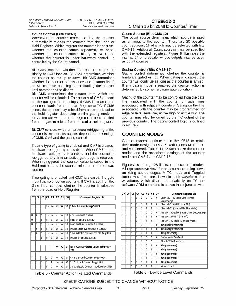
C7 C6 C5 C4 C3 C2 C1 C0 Command Register Bit
0 0 0 E2 E1 G4 G2 G1 Load Data Pointer Commands G1-4 Group Pointer E1-2 Element Pointer
0 0 0 0 0 0 0 0 Reserved 0 0 0 0 0 0 0 1 Counter 1 Mode Register 0 0 0 0 0 0 1 0 Counter 2 Mode Register 0 0 0 0 0 0 1 1 Counter 3 Mode Register 0 0 0 0 0 1 0 0 Counter 4 Mode Register 0 0 0 0 0 1 0 1 Counter 5 Mode Register 0 0 0 0 0 1 1 0 Reserved 0 0 0 0 0 1 1 1 Alarm Register 1 / Control Cycle 0 0 0 0 1 0 0 0 Reserved 0 0 0 0 1 0 0 1 Counter 1 Load Register 0 0 0 0 1 0 1 0 Counter 2 Load Register 0 0 0 0 1 0 1 1 Counter 3 Load Register 0 0 0 0 1 1 0 0 Counter 4 Load Register 0 0 0 0 1 1 0 1 Counter 5 Load Register 0 0 0 0 1 1 1 0 Reserved 0 0 0 0 1 1 1 1 Alarm Register 2 / Control Cycle 0 0 0 1 0 0 0 0 Reserved 0 0 0 1 0 0 0 1 Counter 1 Hold Register 0 0 0 1 0 0 1 0 Counter 2 Hold Register 0 0 0 1 0 0 1 1 Counter 3 Hold Register 0 0 0 1 0 1 0 0 Counter 4 Hold Register 0 0 0 1 0 1 0 1 Counter 5 Hold Register 0 0 0 1 0 1 1 0 Reserved 0 0 0 1 0 1 1 1 Master Mode Register / Control
Cycle 0 0 0 1 1 0 0 0 Reserved 0 0 0 1 1 0 0 1 Hold Register Cycle 0 0 0 1 1 0 1 0 Hold Register Cycle 0 0 0 1 1 0 1 1 Hold Register Cycle 0 0 0 1 1 1 0 0 Hold Register Cycle 0 0 0 1 1 1 0 1 Hold Register Cycle 0 0 0 1 1 1 1 0 Reserved 0 0 0 1 1 1 1 1 Status Register
Table 4 - CTS9513 Data Pointer Commands
6 No Retriggering 7 F1 source selected 8 Positive-true input polarity 9 No Gating
The Counter Mode Register must be loaded while the counter is disarmed.. Table 10 summarizes the Counter Mode Register bit assignments. Output Control (Bits CM0-2) The counter output may be configured to be disabled, programmed to follow the counter terminal count or to toggle its state at each terminal count. The output logic for each counter is shown in Figure 8. The output may be disabled by either placing it in a high impedance state or in a low impedance state to ground. The outputs may also be hardware inhibited with the line. In the Terminal count mode, the output may be programmed to output an active high or active low pulse which is equal to one count source clock period. In the output toggle mode, the output changes state whenever the counter reaches a terminal count. The output state may be initialized with the SET and CLEAR counter commands.
Celeritous Technical Services Corp 800.687.6510 / 806.793.0708 3308 34th St FAX 806.793.0710 Lubbock, Texas 79410 http://www.celeritous.com
SPECIFICATIONS SUBJECT TO CHANGE WITHOUT NOTICE
Copyright 2000 Celeritous Technical Services Corp 9 Rev E Tuesday, September 25,
CTS9513-2 5 Chan 16 bit 20MHz Counter/Timer
Count Control (Bits CM3-7) Whenever the counter reaches a TC, the counter automatically reloads the counter from the Load or Hold Register. Which register the counter loads from, whether the counter counts repeatedly or once, whether the counter counts binary or BCD and whether the counter is under hardware control is controlled by the Count control. Bit CM3 controls whether the counter counts in Binary or BCD fashion. Bit CM4 determines whether the counter counts up or down. Bit CM5 determines whether the counter counts once and disarms itself, or will continue counting and reloading the counter until commanded to disarm. Bit CM6 determines the source from which the counter will be reloaded. The actions of CM6 depend on the gating control settings. If CM6 is cleared, the counter reloads from the Load Register at TC. If CM6 is set, the counter may reload from either the Load or the hold register depending on the gating mode. It may alternate with the Load register or be controlled from the gate to reload from the load or hold register. Bit CM7 controls whether hardware retriggering of the counter is enabled. Its actions depend on the settings of CM5, CM6 and the gating controls. If some type of gating is enabled and CM7 is cleared, hardware retriggering is disabled. When CM7 is set, hardware retriggering is enabled and the counter is retriggered any time an active gate edge is received. When retriggered the counter value is saved in the Hold register and the counter reloaded from the Load register. If no gating is enabled and CM7 is cleared, the gate input has no effect on counting. If CM7 is set then the Gate input controls whether the counter is reloaded from the Load or Hold Register.
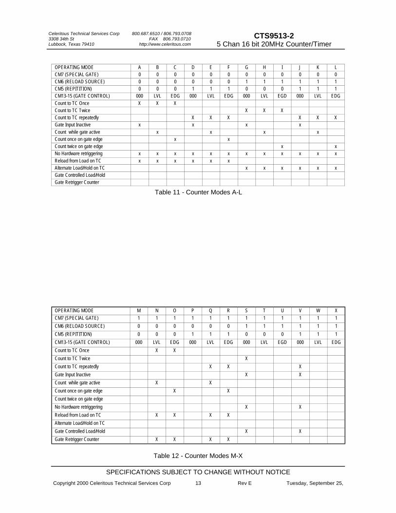
Count Source (Bits CM8-12) The count source determines which source is used as an input to the counter. There are 20 possible count sources, 16 of which may be selected with bits CM8-12. Additional Count sources may be specified with the extended registers. Figure 8 illustrates the internal 24 bit prescaler whose outputs may be used as count sources. Gating Control (Bits CM13-15) Gating control determines whether the counter is hardware gated or not. When gating is disabled the counter will continue as long as the counter is armed. If any gating mode is enabled the counter action is determined by some hardware gate condition. Gating of the counter may be controlled from the gate line associated with the counter or gate lines associated with adjacent counters. Gating on the line associated with the counter may be programmed for edge or level sensitive, active high or active low. The counter may also be gated by the TC output of the previous counter. The gating control logic is outlined in Figure 7. COUNTER MODES Counter modes continue as in the ‘9513 to retain their mode designations A-X, with modes M, P, T, U and V reserved. Tables 11-12 summarize the counter modes and the associated settings of the counter mode bits CM5-7 and CM13-15. Figures 10 through 28 illustrate the counter modes. All representative waveforms assume counting down on rising source edges. A TC mode and Toggled output waveform are shown in each waveform. For waveforms which disarm automatically on TC the software ARM command is shown in conjunction with
C7 C6 C5 C4 C3 C2 C1 C0 Command Register Bit
S5 S4 S3 S2 S1 S1-5 - Counter Group Select
0 0 1 S5 S4 S3 S2 S1 Arm Selected Counters
0 1 0 S5 S4 S3 S2 S1 Load Selected Counters
0 1 1 S5 S4 S3 S2 S1 Load and Arm Selected Counters
1 0 0 S5 S4 S3 S2 S1 Disarm and Save Selected Counters
1 0 1 S5 S4 S3 S2 S1 Save selected counters to Hold Registers
1 1 0 S5 S4 S3 S2 S1 Disarm Selected Counters
N4 N2 N1 N1-4 Counter Group Select (001 = N = 101
1 1 1 0 0 N4 N2 N1 Clear Selected Counter Toggle Out
1 1 1 0 1 N4 N2 N1 Set Selected Counter Toggle Out
1 1 1 1 0 N4 N2 N1 Step Selected Counter (up/down by CM3)
Table 5 - Counter Action Related Commands
C7 C6 C5 C4 C3 C2 C1 C0 Command Register Bit
1 1 1 0 0 0 0 0 Clear MM14 (Enable Data Pointer Sequencing)
1 1 1 0 0 1 1 0 Clear MM12 (FOUT Gate On)
1 1 1 0 0 1 1 1 Clear MM13 (Enable 8 bit Bus Mode)
1 1 1 0 1 0 0 0 Set MM14 (Disable Data Pointer Sequencing)
1 1 1 0 1 1 1 0 Set MM12 (FOUT Gate Off)
1 1 1 0 1 1 1 1 Set MM13 (Enable 16 bit Bus Mode)
1 1 1 1 0 0 0 0 (Originally Reserved)
1 1 1 1 0 1 1 0 (Originally Reserved)
1 1 1 1 0 1 1 1 (Orig Reserved)
1 1 1 1 1 0 0 0 Enable Write Pre-Fetch
1 1 1 1 1 0 0 1 Disable Write Pre-Fetch
1 1 1 1 1 0 1 0 (Orig Reserved)
1 1 1 1 1 0 1 1 (Orig Reserved)
1 1 1 1 1 1 0 0 (Orig Reserved)
1 1 1 1 1 1 0 1 (Orig Reserved)
1 1 1 1 1 1 1 0 (Orig Reserved)
1 1 1 1 1 1 1 1 Master Reset
Table 6 - Device Level Commands
Celeritous Technical Services Corp 800.687.6510 / 806.793.0708 3308 34th St FAX 806.793.0710 Lubbock, Texas 79410 http://www.celeritous.com
SPECIFICATIONS SUBJECT TO CHANGE WITHOUT NOTICE
Copyright 2000 Celeritous Technical Services Corp 10 Rev E Tuesday, September 25,
CTS9513-2 5 Chan 16 bit 20MHz Counter/Timer
S7 S6 S5 S4 S3 S2 S1 S0
CMP2 CMP1 OUT5 OUT4 OUT3 OUT2 OUT1 WP
Comparator Counter Output Status Byte Reflects actual state of
Interrupt Output Pointer Reflects Actual State of Output
Table 7 - Status Register
a Write pulse. Repetitive waveforms do not show the write pulse or ARM command. The letters L and H are used in the figures to denote Load and Hold register values and the letters K and N to denote arbitrary counter values. In all cases, the counter begins counting on the first count source edge following the Write pulse in software triggered modes and the first source edge following a valid gate edge in hardware triggered or enabled modes. In gate controlled modes which inhibit counting, the counter is suspended for any valid source edges that occur after de-assertion of the gate line.
CTS9513AXI-2 ERRATA Although tested extensively to ensure full compliance with the original AM9513Axx device functions and operating modes, several functional anomalies have come to our attention. Both current and potential users of this device should take note of these. Devices Affected: All 1996, 97, 98, 99 and 2000 devices manufactured to date Planned Action: There are no immediate plans to correct these defects until further testing can be completed to detect any further anomalies.
Work-Arounds: There is no current work-around for these problems for existing designs. CRYSTAL OSCILLATOR The CTS9513 does not incorporate a crystal oscilla-tor and must be driven from an external TTL compati-ble oscillator source. COMMAND DATA READ/WRITE DATA LATCH In this implementation of the 9513 data being written to the device is not latched on the rising (trailing) edge of the write strobe. Data in this device is latched into the command and control registers on the low level of the write strobe. This means that the data must be stable up until shortly before the rising edge of the write strobe. This appears to be an artifact of the way the 8 bit sequential write mode was implemented in order to correctly increment the byte pointer and latch the data on the one write strobe. To date we have only seen this create a problem in one instance on an ISA bus Counter/Timer instrumentation card where the ISA bus decoding was incorrectly implemented. In that instance, a delay in de-asserting the chip select was causing the leading edge of a write strobe for another I/O device to appear prior to the trailing edge of the Chip Select signal. This was interpreted as another valid write to the 9513 device causing invalid data to be written to the device.
MM15 MM14 MM13 MM12 MM11 MM10 MM9 MM8 MM7 MM6 MM5 MM4 MM3 MM2 MM1 MM0 SCALE POINT BUS FGATE1 DIV1-8 DIV1-4 DIV1-2 DIV1-1 FOUT1-8 FOUT1-4 FOUT1-2 FOUT1-1 COMP2 COMP1 TOD2 TOD1
Scale Data Data Bus FOUT FOUT Divider FOUT Source Select Comparator Time of Day Mode Mode Pointer Width Mode Mode 0 BIN 0 Enable 0 = 8 0 = On 0000 = Divide by 16 0000 = F1 00 = Disabled 00 = TOD Disabled 1 BCD 1 Disable 1 = 16 1 = Off 0001 = Divide by 1 001 = Source 1 01 = Comparator 1 On 01 = TOD Enabled /5
0010 = Divide by 2 0010 = Source 2 10 = Comparator 2 On 10 = TOD Enabled /6 0011 = Divide by 3 0011 = Source 3 11 = Both On 11 = TOD Enabled /10 0100 = Divide by 4 0100 = Source 4 0101 = Divide by 5 0101 = Source 5 . 0110 = Gate 1 . 0111 = Gate 2 . 1000 = Gate 3 . 1001 = Gate 4 . 1010 = Gate 5 . 1011 = F1 . 1100 = F2 . 1101 = F3 . 1110 = F4 1111 = Divide by 16 1111 = F5
Table 8 - Master and Auxiliary Master Mode Register Definitions
Celeritous Technical Services Corp 800.687.6510 / 806.793.0708 3308 34th St FAX 806.793.0710 Lubbock, Texas 79410 http://www.celeritous.com
SPECIFICATIONS SUBJECT TO CHANGE WITHOUT NOTICE
Copyright 2000 Celeritous Technical Services Corp 11 Rev E Tuesday, September 25,
CTS9513-2 5 Chan 16 bit 20MHz Counter/Timer
Table 9 - CTS9513 Time-of-Day Data Format
C2-15 C2-14 C2-13 C2-12 C2-11 C2-10 C2-9 C2-8 C2-7 C2-6 C2-5 C2-4 C2-3 C2-2 C2-1 C2-0
10's Hours Hours 10's Minutes Minutes
BCD DATA 0 - 23 Hours BCD DATA 0-59 Minutes
C1-15 C1-14 C1-13 C1-12 C1-11 C1-10 C1-9 C1-8 C1-7 C1-6 C1-5 C1-4 C1-3 C1-2 C1-1 C1-0
10's Seconds Seconds 10th Seconds Division Factor (5, 6, 10)
BCD DATA 0.0 - 59.9 Seconds
Table 10 - CTS9513 Counter Mode and Auxiliary Counter Mode Register Bit Assignments
CM15 CM14 CM13 CM12 CM11 CM10 CM9 CM8 CM7 CM6 CM5 CM4 CM3 CM2 CM1 CM0
GCTL3 GCTL2 GCTL1 EDGE SRC1-8 SRC1-4 SRC1-2 SRC1-1 GATE RELOAD REPEAT COUNT DIR OUT4 OUT2 OUT1
Gate Control Edge Count Source Selection Gate Reload Repeat Count Count Output Control 000 No Gating Mode 0000 = TC N-1 Mode Mode Mode Mode Direction 000 = Inactive, Output Low 001 Active High, TC N-1 0 Rising 0001 = Source 1 0 = Off 0 = Load 0 Once 0 Binary 0 Down 001 = Active High on TC 010 Active High Level GateN+1
1 Falling 0010 = Source 2 1 = On 1 = Both 1 Repeat 1 BCD 1 Up 010 = TC Toggled
011 Active High Level GateN-1 0011 = Source 3 011 = Illegal 100 Active High Level GateN 0100 = Source 4 100 = Inactive, Output High Z 101 Active Low Level GateN 0101 = Source 5 101 = Active Low on TC 110 Active High Edge GateN 0110 = Gate 1 110 = Illegal 111 Active Low Edge GateN 0111 = Gate 2 "111 = Illegal 1000 = Gate 3 1001 = Gate 4 1010 = Gate 5 1011 = F1 1100 = F2 1101 = F3 1110 = F4 1111 = F5
MUXA
BO
R
S
Q
Q
MUXA
BO
MUXA
BO
CLK
D
S
C
Q
Q
INT MODE
INT CLEAR
COUNTER TC
OUTPUT SET
OUTPUT CLEAR
TC/TOGGLE
COMPARATOR
ALARM EN
OUTPUT POL
OUTPUT LOW
OUTPUT INHIBIT
TRISTATE CNTL
OUTPUT
TC OUT
INT OUT
Figure 7 - Counter Output Section Block Diagram
Celeritous Technical Services Corp 800.687.6510 / 806.793.0708 3308 34th St FAX 806.793.0710 Lubbock, Texas 79410 http://www.celeritous.com
SPECIFICATIONS SUBJECT TO CHANGE WITHOUT NOTICE
Copyright 2000 Celeritous Technical Services Corp 12 Rev E Tuesday, September 25,
CTS9513-2 5 Chan 16 bit 20MHz Counter/Timer
Figure 9 - CTS9513 Counter Gating Input Logic Block Diagram
MODE V (FSK) ERROR An error in implementing the special gate function prevents the implementation of Mode V (FSK Generator). The gate level is supposed to control whether the counter is reloaded from the LOAD or HOLD register to determine the output rate generator frequency and allow switching between two frequencies to produce Frequency Shift Keying (FSK) modulation. When programmed for Mode V, the current device Revision will reload only from the HOLD register regardless of the state of the GATE input. This appears to be a general problem with the “special gate” function that controls reloading of the counter from the Load or Hold register depending on the state of the gate.
MODE J ERROR The counters will not allow a count of 1 to be set in the load and/or hold registers
COUNTER SAVE ERRORS Due to the asynchronous nature of this part (and to an extent the original AMD AM9513) we have seen errors in the saved counter data when a counter save command is issued. This occurs when the write strobe rising edge for a save command occurs simul-taneously with a counter clock edge and the counter tries to save the current count while also trying to in-crement or decrement the counter. The only solid solution we have found for this proble is for the bus clock to also be the master clock or to be phased locked to it in order for the timing of bus read/write cycles to be deterministic with respect to the counter clock edges.
Figure 8 - CTS9513 Counter Internal Prescaler Block Diagram
4 BITS 4 BITS 4 BITS 4 BITS
F1
F2
F3
F4
F5CLK IN
FREQUENCY BCD SCALING BINARY SCALING
F1F2F3F4F5
CLK IN CLK INCLK / 16CLK / 256CLK / 4096CLK / 65536
CLK / 10CLK / 100CLK / 1000CLK / 10000
COUNTER MODEREGISTER
GATE INPUT MUXAND POLARITY
SELECT
TC-1GATE -1GATEGATE+1
GATE EN
EDGE AND LEVEL GATECONTROL COUNTER
Celeritous Technical Services Corp 800.687.6510 / 806.793.0708 3308 34th St FAX 806.793.0710 Lubbock, Texas 79410 http://www.celeritous.com
SPECIFICATIONS SUBJECT TO CHANGE WITHOUT NOTICE
Copyright 2000 Celeritous Technical Services Corp 13 Rev E Tuesday, September 25,
CTS9513-2 5 Chan 16 bit 20MHz Counter/Timer
OPERATING MODE M N O P Q R S T U V W X CM7 (SPECIAL GATE) 1 1 1 1 1 1 1 1 1 1 1 1
CM6 (RELOAD SOURCE) 0 0 0 0 0 0 1 1 1 1 1 1
CM5 (REPITITION) 0 0 0 1 1 1 0 0 0 1 1 1
CM13-15 (GATE CONTROL) 000 LVL EDG 000 LVL EDG 000 LVL EGD 000 LVL EDG
Count to TC Once X X
Count to TC Twice X
Count to TC repeatedly X X X
Gate Input Inactive X X
Count while gate active X X
Count once on gate edge X X
Count twice on gate edge
No Hardware retriggering X X
Reload from Load on TC X X X X
Alternate Load/Hold on TC
Gate Controlled Load/Hold X X
Gate Retrigger Counter X X X X
Table 12 - Counter Modes M-X
OPERATING MODE A B C D E F G H I J K L CM7 (SPECIAL GATE) 0 0 0 0 0 0 0 0 0 0 0 0 CM6 (RELOAD SOURCE) 0 0 0 0 0 0 1 1 1 1 1 1 CM5 (REPITITION) 0 0 0 1 1 1 0 0 0 1 1 1 CM13-15 (GATE CONTROL) 000 LVL EDG 000 LVL EDG 000 LVL EGD 000 LVL EDG Count to TC Once X X X Count to TC Twice X X X Count to TC repeatedly X X X X X X Gate Input Inactive x x x x Count while gate active x x x x Count once on gate edge x x Count twice on gate edge x x No Hardware retriggering x x x x x x x x x x x x Reload from Load on TC x x x x x x Alternate Load/Hold on TC x x x x x x Gate Controlled Load/Hold Gate Retrigger Counter
Table 11 - Counter Modes A-L
Celeritous Technical Services Corp 800.687.6510 / 806.793.0708 3308 34th St FAX 806.793.0710 Lubbock, Texas 79410 http://www.celeritous.com
SPECIFICATIONS SUBJECT TO CHANGE WITHOUT NOTICE
Copyright 2000 Celeritous Technical Services Corp 14 Rev E Tuesday, September 25,
CTS9513-2 5 Chan 16 bit 20MHz Counter/Timer
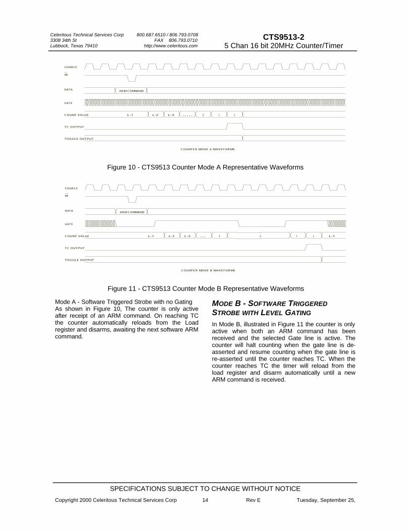
Mode A - Software Triggered Strobe with no Gating As shown in Figure 10, The counter is only active after receipt of an ARM command. On reaching TC the counter automatically reloads from the Load register and disarms, awaiting the next software ARM command.
MODE B - SOFTWARE TRIGGERED STROBE WITH LEVEL GATING In Mode B, illustrated in Figure 11 the counter is only active when both an ARM command has been received and the selected Gate line is active. The counter will halt counting when the gate line is de-asserted and resume counting when the gate line is re-asserted until the counter reaches TC. When the counter reaches TC the timer will reload from the load register and disarm automatically until a new ARM command is received.
SOURCE
WR
DATA ARM COMMAND
L-1 L-2 L-3 ..... 2 1 LCOUNT VALUE
TC OUTPUT
TOGGLE OUTPUT
COUNTER MODE A WAVEFORMS
GATE
Figure 10 - CTS9513 Counter Mode A Representative Waveforms
SOURCE
WR
DATA ARM COMMAND
GATE
L-1L123...L-3L-2L-1COUNT VALUE
TC OUTPUT
TOGGLE OUTPUT
COUNTER MODE B WAVEFORMS
Figure 11 - CTS9513 Counter Mode B Representative Waveforms
Celeritous Technical Services Corp 800.687.6510 / 806.793.0708 3308 34th St FAX 806.793.0710 Lubbock, Texas 79410 http://www.celeritous.com
SPECIFICATIONS SUBJECT TO CHANGE WITHOUT NOTICE
Copyright 2000 Celeritous Technical Services Corp 15 Rev E Tuesday, September 25,
CTS9513-2 5 Chan 16 bit 20MHz Counter/Timer
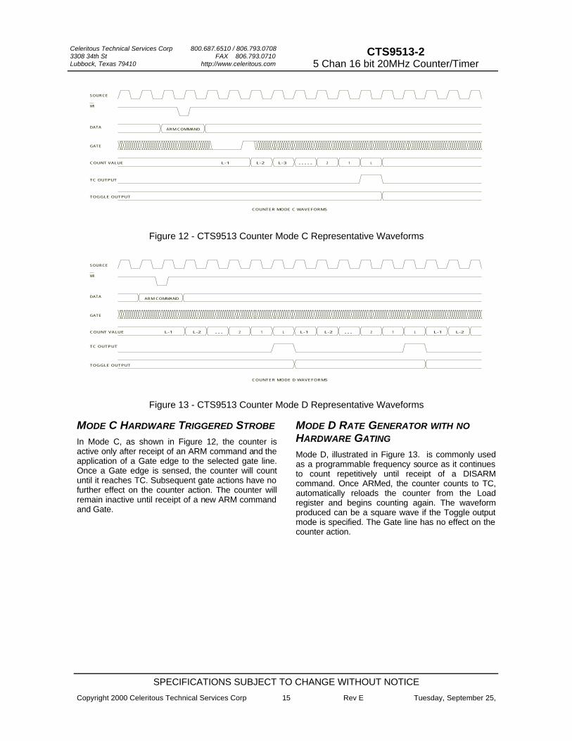
SOURCE
WR
DATA ARM COMMAND
L-1 L-2 L-3 ..... 2 1 LCOUNT VALUE
TC OUTPUT
TOGGLE OUTPUT
GATE
COUNTER MODE C WAVEFORMS
Figure 12 - CTS9513 Counter Mode C Representative Waveforms
SOURCE
WR
DATA ARM COMMAND
GATE
L-1 L-2 ... 2 1 L L-1 L-2 ... 2 1 L L-1 L-2COUNT VALUE
TC OUTPUT
TOGGLE OUTPUT
COUNTER MODE D WAVEFORMS
Figure 13 - CTS9513 Counter Mode D Representative Waveforms
MODE D RATE GENERATOR WITH NO HARDWARE GATING Mode D, illustrated in Figure 13. is commonly used as a programmable frequency source as it continues to count repetitively until receipt of a DISARM command. Once ARMed, the counter counts to TC, automatically reloads the counter from the Load register and begins counting again. The waveform produced can be a square wave if the Toggle output mode is specified. The Gate line has no effect on the counter action.
MODE C HARDWARE TRIGGERED STROBE In Mode C, as shown in Figure 12, the counter is active only after receipt of an ARM command and the application of a Gate edge to the selected gate line. Once a Gate edge is sensed, the counter will count until it reaches TC. Subsequent gate actions have no further effect on the counter action. The counter will remain inactive until receipt of a new ARM command and Gate.
Celeritous Technical Services Corp 800.687.6510 / 806.793.0708 3308 34th St FAX 806.793.0710 Lubbock, Texas 79410 http://www.celeritous.com
SPECIFICATIONS SUBJECT TO CHANGE WITHOUT NOTICE
Copyright 2000 Celeritous Technical Services Corp 16 Rev E Tuesday, September 25,
CTS9513-2 5 Chan 16 bit 20MHz Counter/Timer
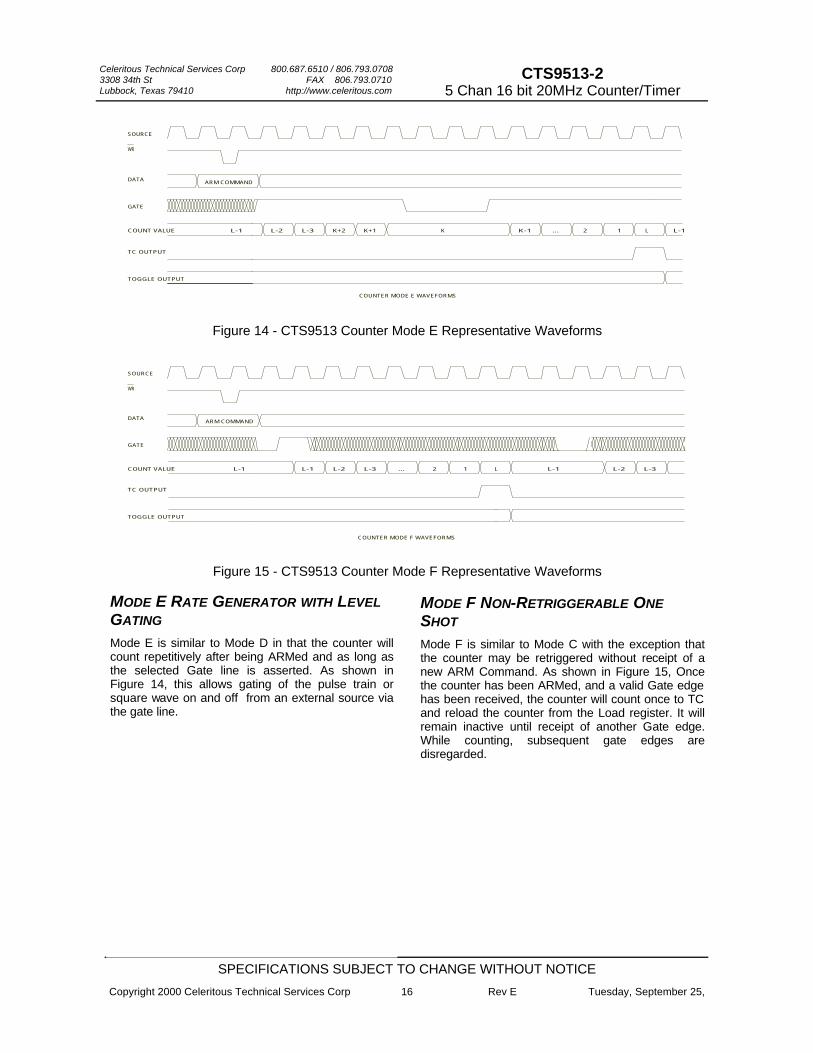
MODE E RATE GENERATOR WITH LEVEL GATING Mode E is similar to Mode D in that the counter will count repetitively after being ARMed and as long as the selected Gate line is asserted. As shown in Figure 14, this allows gating of the pulse train or square wave on and off from an external source via the gate line.
SOURCE
WR
DATA ARM COMMAND
GATE
COUNT VALUE
TC OUTPUT
TOGGLE OUTPUT
COUNTER MODE E WAVEFORMS
L-1 L-2 L-3 K+2 K+1 K K-1 ... 2 1 L L-1
Figure 14 - CTS9513 Counter Mode E Representative Waveforms
SOURCE
WR
DATAARM COMMAND
GATE
L-1COUNT VALUE
TC OUTPUT
TOGGLE OUTPUT
COUNTER MODE F WAVEFORMS
L12...L-3L-2L-1 L-1 L-2 L-3
Figure 15 - CTS9513 Counter Mode F Representative Waveforms
MODE F NON-RETRIGGERABLE ONE SHOT Mode F is similar to Mode C with the exception that the counter may be retriggered without receipt of a new ARM Command. As shown in Figure 15, Once the counter has been ARMed, and a valid Gate edge has been received, the counter will count once to TC and reload the counter from the Load register. It will remain inactive until receipt of another Gate edge. While counting, subsequent gate edges are disregarded.
Celeritous Technical Services Corp 800.687.6510 / 806.793.0708 3308 34th St FAX 806.793.0710 Lubbock, Texas 79410 http://www.celeritous.com
SPECIFICATIONS SUBJECT TO CHANGE WITHOUT NOTICE
Copyright 2000 Celeritous Technical Services Corp 17 Rev E Tuesday, September 25,
CTS9513-2 5 Chan 16 bit 20MHz Counter/Timer
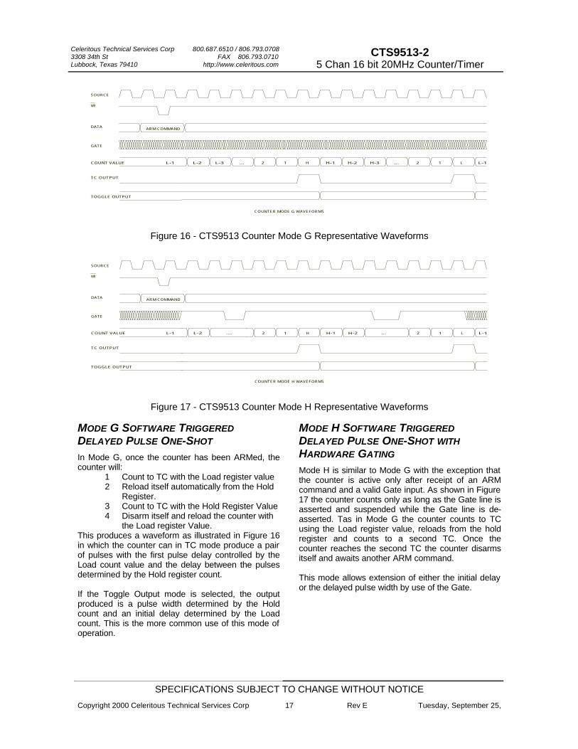
MODE G SOFTWARE TRIGGERED DELAYED PULSE ONE-SHOT In Mode G, once the counter has been ARMed, the counter will:
1 Count to TC with the Load register value 2 Reload itself automatically from the Hold
Register. 3 Count to TC with the Hold Register Value 4 Disarm itself and reload the counter with
the Load register Value. This produces a waveform as illustrated in Figure 16 in which the counter can in TC mode produce a pair of pulses with the first pulse delay controlled by the Load count value and the delay between the pulses determined by the Hold register count. If the Toggle Output mode is selected, the output produced is a pulse width determined by the Hold count and an initial delay determined by the Load count. This is the more common use of this mode of operation.
SOURCE
WR
DATA ARM COMMAND
GATE
L-1COUNT VALUE
TC OUTPUT
TOGGLE OUTPUT
COUNTER MODE G WAVEFORMS
L-1L12...H-3H-2H-1H12...L-3L-2
Figure 16 - CTS9513 Counter Mode G Representative Waveforms
SOURCE
WR
DATA ARM COMMAND
GATE
L-1COUNT VALUE
TC OUTPUT
TOGGLE OUTPUT
L-1L12H-2H-1H12L-2
COUNTER MODE H WAVEFORMS
.... ...
Figure 17 - CTS9513 Counter Mode H Representative Waveforms
MODE H SOFTWARE TRIGGERED DELAYED PULSE ONE-SHOT WITH HARDWARE GATING Mode H is similar to Mode G with the exception that the counter is active only after receipt of an ARM command and a valid Gate input. As shown in Figure 17 the counter counts only as long as the Gate line is asserted and suspended while the Gate line is de-asserted. Tas in Mode G the counter counts to TC using the Load register value, reloads from the hold register and counts to a second TC. Once the counter reaches the second TC the counter disarms itself and awaits another ARM command. This mode allows extension of either the initial delay or the delayed pulse width by use of the Gate.
Celeritous Technical Services Corp 800.687.6510 / 806.793.0708 3308 34th St FAX 806.793.0710 Lubbock, Texas 79410 http://www.celeritous.com
SPECIFICATIONS SUBJECT TO CHANGE WITHOUT NOTICE
Copyright 2000 Celeritous Technical Services Corp 18 Rev E Tuesday, September 25,
CTS9513-2 5 Chan 16 bit 20MHz Counter/Timer
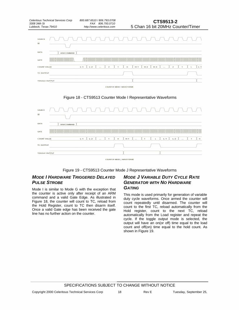
MODE I HARDWARE TRIGGERED DELAYED PULSE STROBE Mode I is similar to Mode G with the exception that the counter is active only after receipt of an ARM command and a valid Gate Edge. As illustrated in Figure 18, the counter will count to TC, reload from the Hold Register, count to TC then disarm itself. Once a valid Gate edge has been received the gate line has no further action on the counter.
SOURCE
WR
DATAARM COMMAND
GATE
COUNT VALUE
TC OUTPUT
TOGGLE OUTPUT
L-1L12...H-3H-2H-1H12...
COUNTER MODE I WAVEFORMS
L-2L-1
Figure 18 - CTS9513 Counter Mode I Representative Waveforms
SOURCE
WR
DATAARM COMMAND
GATE
COUNT VALUE
TC OUTPUT
TOGGLE OUTPUT
...L-2L-1
COUNTER MODE J WAVEFORMS
1 H H-1 ... 1 L L-1 L-2 ... 1 H
Figure 19 - CTS9513 Counter Mode J Representative Waveforms
MODE J VARIABLE DUTY CYCLE RATE GENERATOR WITH NO HARDWARE GATING This mode is used primarily for generation of variable duty cycle waveforms. Once armed the counter will count repeatedly until disarmed. The counter will count to the first TC, reload automatically from the Hold register, count to the next TC, reload automatically from the Load register and repeat the cycle. If the toggle output mode is selected, the output will have an on(or off) time equal to the load count and off(on) time equal to the hold count. As shown in Figure 19.
Celeritous Technical Services Corp 800.687.6510 / 806.793.0708 3308 34th St FAX 806.793.0710 Lubbock, Texas 79410 http://www.celeritous.com
SPECIFICATIONS SUBJECT TO CHANGE WITHOUT NOTICE
Copyright 2000 Celeritous Technical Services Corp 19 Rev E Tuesday, September 25,
CTS9513-2 5 Chan 16 bit 20MHz Counter/Timer
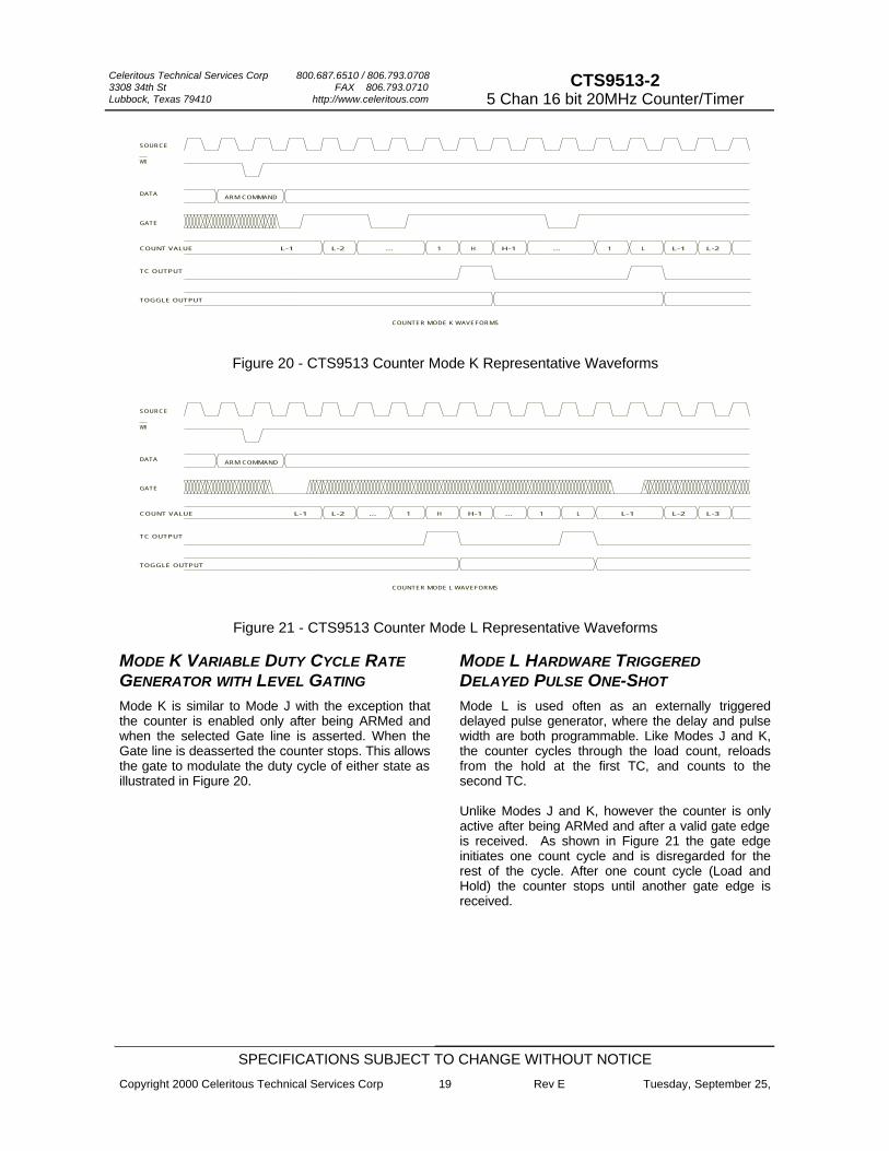
MODE K VARIABLE DUTY CYCLE RATE GENERATOR WITH LEVEL GATING Mode K is similar to Mode J with the exception that the counter is enabled only after being ARMed and when the selected Gate line is asserted. When the Gate line is deasserted the counter stops. This allows the gate to modulate the duty cycle of either state as illustrated in Figure 20.
SOURCE
WR
DATAARM COMMAND
GATE
COUNT VALUE
TC OUTPUT
TOGGLE OUTPUT
COUNTER MODE K WAVEFORMS
H H-1 ... 1 L1...L-2L-1 L-1 L-2
Figure 20 - CTS9513 Counter Mode K Representative Waveforms
SOURCE
WR
DATA ARM COMMAND
GATE
COUNT VALUE
TC OUTPUT
TOGGLE OUTPUT
COUNTER MODE L WAVEFORMS
H1...L-2L-1 H-1 ... 1 L L-1 L-2 L-3
Figure 21 - CTS9513 Counter Mode L Representative Waveforms
MODE L HARDWARE TRIGGERED DELAYED PULSE ONE-SHOT Mode L is used often as an externally triggered delayed pulse generator, where the delay and pulse width are both programmable. Like Modes J and K, the counter cycles through the load count, reloads from the hold at the first TC, and counts to the second TC. Unlike Modes J and K, however the counter is only active after being ARMed and after a valid gate edge is received. As shown in Figure 21 the gate edge initiates one count cycle and is disregarded for the rest of the cycle. After one count cycle (Load and Hold) the counter stops until another gate edge is received.
Celeritous Technical Services Corp 800.687.6510 / 806.793.0708 3308 34th St FAX 806.793.0710 Lubbock, Texas 79410 http://www.celeritous.com
SPECIFICATIONS SUBJECT TO CHANGE WITHOUT NOTICE
Copyright 2000 Celeritous Technical Services Corp 20 Rev E Tuesday, September 25,
CTS9513-2 5 Chan 16 bit 20MHz Counter/Timer
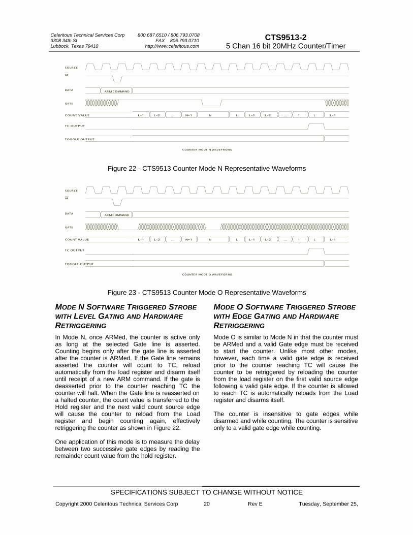
MODE N SOFTWARE TRIGGERED STROBE WITH LEVEL GATING AND HARDWARE RETRIGGERING In Mode N, once ARMed, the counter is active only as long at the selected Gate line is asserted. Counting begins only after the gate line is asserted after the counter is ARMed. If the Gate line remains asserted the counter will count to TC, reload automatically from the load register and disarm itself until receipt of a new ARM command. If the gate is deasserted prior to the counter reaching TC the counter will halt. When the Gate line is reasserted on a halted counter, the count value is transferred to the Hold register and the next valid count source edge will cause the counter to reload from the Load register and begin counting again, effectively retriggering the counter as shown in Figure 22. One application of this mode is to measure the delay between two successive gate edges by reading the remainder count value from the hold register.
SOURCE
WR
DATA ARM COMMAND
GATE
COUNT VALUE
TC OUTPUT
TOGGLE OUTPUT
L-1 L-2 ... N+1 N L L-1 L-2 ... 1 L L-1
COUNTER MODE N WAVEFROMS
Figure 22 - CTS9513 Counter Mode N Representative Waveforms
SOURCE
WR
DATA ARM COMMAND
GATE
COUNT VALUE
TC OUTPUT
TOGGLE OUTPUT
L-1 L-2 ... N+1 N L L-1 L-2 ... 1 L L-1
COUNTER MODE O WAVEFORMS
Figure 23 - CTS9513 Counter Mode O Representative Waveforms
MODE O SOFTWARE TRIGGERED STROBE WITH EDGE GATING AND HARDWARE RETRIGGERING Mode O is similar to Mode N in that the counter must be ARMed and a valid Gate edge must be received to start the counter. Unlike most other modes, however, each time a valid gate edge is received prior to the counter reaching TC will cause the counter to be retriggered by reloading the counter from the load register on the first valid source edge following a valid gate edge. If the counter is allowed to reach TC is automatically reloads from the Load register and disarms itself. The counter is insensitive to gate edges while disarmed and while counting. The counter is sensitive only to a valid gate edge while counting.
Celeritous Technical Services Corp 800.687.6510 / 806.793.0708 3308 34th St FAX 806.793.0710 Lubbock, Texas 79410 http://www.celeritous.com
SPECIFICATIONS SUBJECT TO CHANGE WITHOUT NOTICE
Copyright 2000 Celeritous Technical Services Corp 21 Rev E Tuesday, September 25,
CTS9513-2 5 Chan 16 bit 20MHz Counter/Timer
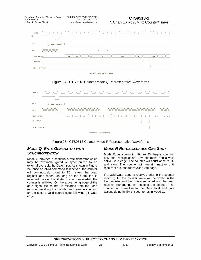
MODE Q RATE GENERATOR WITH SYNCHRONIZATION Mode Q provides a continuous rate generator which may be externally gated or synchronized to an external event via the Gate input. As shown in Figure 24, once an ARM command is received, the counter will continuously count to TC, reload the Load register and repeat as long as the Gate line is asserted. While the Gate line is deasserted the counter is inhibited. On the active going edge of the gate signal the counter is reloaded from the Load register, resetting the counter and resume counting on the second valid source edge following the Gate edge.
SOURCE
WR
DATA ARM COMMAND
GATE
COUNT VALUE
TC OUTPUT
TOGGLE OUTPUT
L-1 L-2 ... N+1 N L L-1 ... 1 L L-1 L-2
COUNTER MODE Q WAVEFORMS
Figure 24 - CTS9513 Counter Mode Q Representative Waveforms
SOURCE
WR
DATAARM COMMAND
GATE
COUNT VALUE
TC OUTPUT
TOGGLE OUTPUT
L-1 L-2 ...
COUNTER MODE R WAVEFORMS
L1N+2 N+1 N L L-1 .. L-2L-1
Figure 25 - CTS9513 Counter Mode R Representative Waveforms
MODE R RETRIGGERABLE ONE-SHOT Mode R, as shown in Figure 25, begins counting only after receipt of an ARM command and a valid active Gate edge. The counter will count once to TC and stop. The counter will remain inactive until receipt of a subsequent valid Gate edge. If a valid Gate Edge is received prior to the counter reaching TC the counter value will be saved in the Hold register and the counter reloaded from the Load register, retriggering or resetting the counter. The counter in insensitive to the Gate level and gate actions do no inhibit the counter as in Mode Q.
Celeritous Technical Services Corp 800.687.6510 / 806.793.0708 3308 34th St FAX 806.793.0710 Lubbock, Texas 79410 http://www.celeritous.com
SPECIFICATIONS SUBJECT TO CHANGE WITHOUT NOTICE
Copyright 2000 Celeritous Technical Services Corp 22 Rev E Tuesday, September 25,
CTS9513-2 5 Chan 16 bit 20MHz Counter/Timer
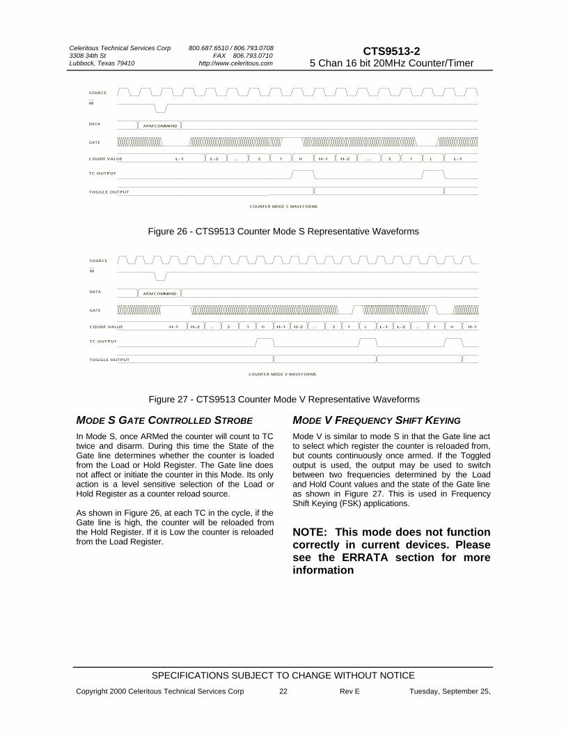
MODE S GATE CONTROLLED STROBE In Mode S, once ARMed the counter will count to TC twice and disarm. During this time the State of the Gate line determines whether the counter is loaded from the Load or Hold Register. The Gate line does not affect or initiate the counter in this Mode. Its only action is a level sensitive selection of the Load or Hold Register as a counter reload source. As shown in Figure 26, at each TC in the cycle, if the Gate line is high, the counter will be reloaded from the Hold Register. If it is Low the counter is reloaded from the Load Register.
SOURCE
WR
DATA ARM COMMAND
GATE
COUNT VALUE
TC OUTPUT
TOGGLE OUTPUT
L-1 L-2 ... 2 1 H H-1 H-2 ... 2 1 L L-1
COUNTER MODE S WAVEFORMS
Figure 26 - CTS9513 Counter Mode S Representative Waveforms
SOURCE
WR
DATA ARM COMMAND
GATE
COUNT VALUE
TC OUTPUT
TOGGLE OUTPUT
H-1 H-2 .. 2 1 H H-1 H-2 .. 2 1 L L-1 L-2 .. 1 H H-1
COUNTER MODE V WAVEFORMS
Figure 27 - CTS9513 Counter Mode V Representative Waveforms
MODE V FREQUENCY SHIFT KEYING Mode V is similar to mode S in that the Gate line act to select which register the counter is reloaded from, but counts continuously once armed. If the Toggled output is used, the output may be used to switch between two frequencies determined by the Load and Hold Count values and the state of the Gate line as shown in Figure 27. This is used in Frequency Shift Keying (FSK) applications.
NOTE: This mode does not function correctly in current devices. Please see the ERRATA section for more information
Celeritous Technical Services Corp 800.687.6510 / 806.793.0708 3308 34th St FAX 806.793.0710 Lubbock, Texas 79410 http://www.celeritous.com
SPECIFICATIONS SUBJECT TO CHANGE WITHOUT NOTICE
Copyright 2000 Celeritous Technical Services Corp 23 Rev E Tuesday, September 25,
CTS9513-2 5 Chan 16 bit 20MHz Counter/Timer
SOURCE
WR
DATA ARM COMMAND
GATE
COUNT VALUE
TC OUTPUT
TOGGLE OUTPUT
HOLD REG
L-1 L-2 ... N+1 N N-1 N-2 .. K+2 K+1 K K-1 .. 1 L L-1 L-2
L N K L
COUNTER MODE X WAVEFORMS
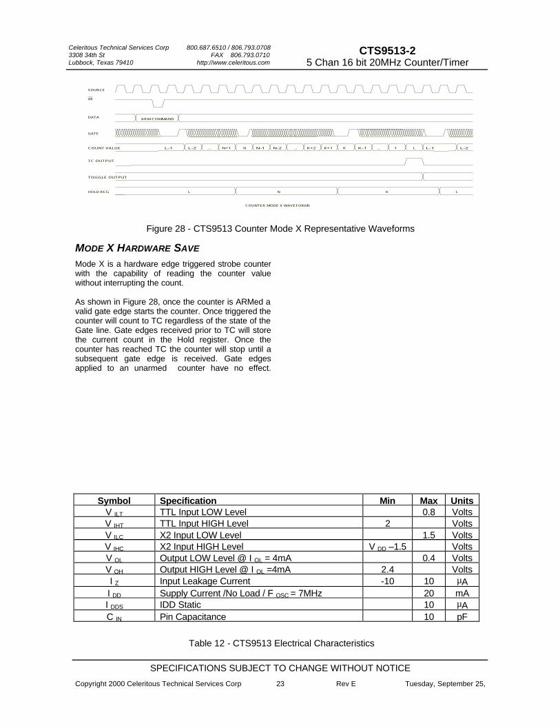
Figure 28 - CTS9513 Counter Mode X Representative Waveforms
MODE X HARDWARE SAVE Mode X is a hardware edge triggered strobe counter with the capability of reading the counter value without interrupting the count. As shown in Figure 28, once the counter is ARMed a valid gate edge starts the counter. Once triggered the counter will count to TC regardless of the state of the Gate line. Gate edges received prior to TC will store the current count in the Hold register. Once the counter has reached TC the counter will stop until a subsequent gate edge is received. Gate edges applied to an unarmed counter have no effect.
Symbol Specification Min Max Units V ILT TTL Input LOW Level 0.8 Volts V IHT TTL Input HIGH Level 2 Volts V ILC X2 Input LOW Level 1.5 Volts V IHC X2 Input HIGH Level V DD –1.5 Volts V OL Output LOW Level @ I OL = 4mA 0.4 Volts V OH Output HIGH Level @ I OL =4mA 2.4 Volts I Z Input Leakage Current -10 10 µA I DD Supply Current /No Load / F OSC = 7MHz 20 mA I DDS IDD Static 10 µA C IN Pin Capacitance 10 pF
Table 12 - CTS9513 Electrical Characteristics
Celeritous Technical Services Corp 800.687.6510 / 806.793.0708 3308 34th St FAX 806.793.0710 Lubbock, Texas 79410 http://www.celeritous.com
SPECIFICATIONS SUBJECT TO CHANGE WITHOUT NOTICE
Copyright 2000 Celeritous Technical Services Corp 24 Rev E Tuesday, September 25,
CTS9513-2 5 Chan 16 bit 20MHz Counter/Timer
COUNT SOURCE
GATE
CS
C/D
RD
WR
DATA
OUT
Tehrl Trheh Tehwh Twheh
Tgvwh Twhgv
Tslrl TrhshTslwh
Twhsh
Tavrl TrhaxTavwh Twhax
Trlrh Trhrl Twhrl
Trhwl Twlwh Twhwl
Twhwl
Trlqv
Trlqx
Trhqz
Trhqx Tdvwh Twhdx
Twhyv
Figure 30 - Bus Timing Diagram
COUNT SOURCE
GATE
FOUT
OUT
X2
FN
FN + 1
Teleh
Teheh
TehelTgveh Tehgv
Tehfv
Tgvgv
Tehyv
Tchch
Tchcl
Tfn
Tclch
Figure 31 - Counter Timing Diagram
Celeritous Technical Services Corp 800.687.6510 / 806.793.0708 3308 34th St FAX 806.793.0710 Lubbock, Texas 79410 http://www.celeritous.com
SPECIFICATIONS SUBJECT TO CHANGE WITHOUT NOTICE
Copyright 2000 Celeritous Technical Services Corp 25 Rev E Tuesday, September 25,
CTS9513-2 5 Chan 16 bit 20MHz Counter/Timer
NOTES 1. Any Input transition that occurs before this minimum setup
requirement will be reflected in the contents read from the status register
2. Any Input transition that occurs before this minimum setup requirement will act on the counter before the execution of the operation initiated by the write and the counter may be off by one count
3. Any input transition that occurs after this minimum hold time is guaranteed to not influence the contents read from the status register on the current read operation
4. Any input transition that occurs after this minimum hold time is guaranteed to be seen by the counter as occurring after the action initiated by the write operation and the counter may be off by one count.
5. This parameter applies to cases where the write operation causes a change in the output bit.
6. The enabled count source is one of F1-F5, TCN-1 SRC1-SRC5 or GATE1-GATE 5, as selected in the applicable Counter Mode register. The timing diagram assumes the counter counts on rising source edges. The timing specifications are the same for falling-edge counting.
7. This parameter applies to edge gating (CM15-CM13=110 or 111) and gating when both CM7=1 and CM15-CM13?000. This parameter represents the minimum GATE pulse width needed to ensure that the pulse initiates counting or counter reloading.
8. This parameter applies to both edge and level gating (CM15-CM13=001 through 111 and CM7 =0). This parameter represents the minimum setup or hold times to ensure that the Gate input is seen at the intended level on the active source
edge and the counter may be off by one count. 9. This parameter assumes that the GATENA input is unused
(16-bit bus mode) or is tied high. In cases where the GATENA input is used, this timing specification must be met by both the GATE and GATENA inputs.
10. Signals F1-F5 cannot be directly monitored by the user. The phase difference between these signals will manifest itself by causing counters using two different F signals to count at different times on nominally simultaneous transitions in the F signals. F1=X2.
11. This timing specification assumes that CS is active whenever RD or WR are active. CS may be held active indefinitely.
12. This parameter assumes X2 is driven from an external gate with a square wave.
13. This parameter assumes that the write operation is to the command register.
14. This timing specification applies to single-action commands only (e.g. LOAD, ARM, SAVE, etc.) For double action commands such as LOAD AND ARM and DISARM AND SAVE, TWHEH minimum = 700ns.
15. In short data write mode, TWHRL and TWHWL minimum = 1000 ns.
16. This parameter applies to the hardware retrigger/save modes N, O, Q, R, and X (CM7 = 1 and CM15-CM13<>000). This parameter ensures that the gating pulse initiates a hardware retrigger/save operation.
17. This parameter applies to hardware load source select modes S and V (CM7 = 1 and CM15-CM13=000). This parameter represents the minimum hold time to ensure that the GATE input selects the correct load source on the active source edge.
Param Description Figure Min Typ MaxTavrl C/D Valid to Read Low 2 15Tavwh C/D Valid to Write High 2 30Tdvwh Data In Valid to Write High 2 40Tehrl Count Source High to Read (setup time) Note 2,7 2 100Tehwh Count Source High to Write High (setup time) Note 3,7 2 50Tgvwh Gate valid to Write High Note 3,10 2 0Trhax Read High to C/D don't Care 2 0Trheh Read High to Count Source High Note 4,7 2 0Trhqx Read High to Data Out Invalid 2 20Trhqz Read High to Data Out Hi-Z (Bus Release Time) 2 40 Trhrl Read High to Read Low (Read Recovery Time) 2 500 Trhsh Read High to CS High Note 12 2 0 Trhwl Read High to Write Low (Read Recovery Time) 2 500 Trlqv Read Low to Data Out Valid 2 50 Trlqx Read Low to Data Bus Driven (Bus Drive Time) 2 20 Trlrh Read Low to Read High (Read Pulse Duration) Note 12 2 80Tslrl CS Low to Read Low Note 12 2 10Tslwh CS Low to Write High Note 12 2 80Twhax Write High to C/D Don't Care 2 0 Twhdx Write High to Data In Don't Care 2 0Twheh Write High to Count Source High Note 5, 7, 14, 15 2 200Twhgv Write High to Gate valid Note 5, 10, 14 2 200Twhrl Write High to Read Low (Write Recovery Time) Note 16 2 500Twhsh Write High to CS High Note 12 2 0Twhwl Write High to Write Low (Write Recovery Time) Note 16 2 500Twhyv Write High to Out Valid Note 6, 14 2 300 Twlwh Write Low to Write High (Write Pulse Duration) Note 12 2 75
Table 14 - Bus Timing Specifications
Celeritous Technical Services Corp 800.687.6510 / 806.793.0708 3308 34th St FAX 806.793.0710 Lubbock, Texas 79410 http://www.celeritous.com
SPECIFICATIONS SUBJECT TO CHANGE WITHOUT NOTICE
Copyright 2000 Celeritous Technical Services Corp 26 Rev E Tuesday, September 25,
CTS9513-2 5 Chan 16 bit 20MHz Counter/Timer
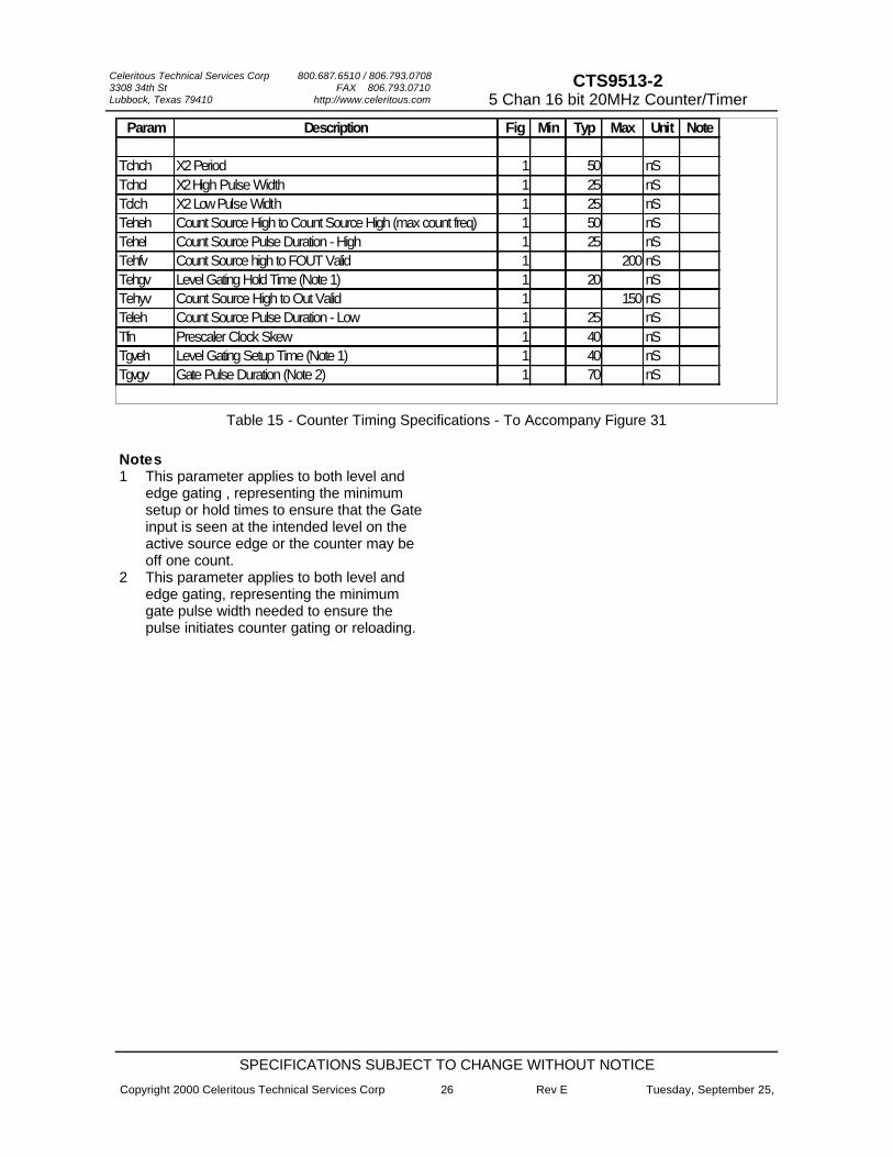
Param Description Fig Min Typ Max Unit Note
Tchch X2 Period 1 50 nSTchcl X2 High Pulse Width 1 25 nSTclch X2 Low Pulse Width 1 25 nSTeheh Count Source High to Count Source High (max count freq) 1 50 nSTehel Count Source Pulse Duration - High 1 25 nSTehfv Count Source high to FOUT Valid 1 200 nSTehgv Level Gating Hold Time (Note 1) 1 20 nSTehyv Count Source High to Out Valid 1 150 nSTeleh Count Source Pulse Duration - Low 1 25 nSTfn Prescaler Clock Skew 1 40 nSTgveh Level Gating Setup Time (Note 1) 1 40 nSTgvgv Gate Pulse Duration (Note 2) 1 70 nS
Table 15 - Counter Timing Specifications - To Accompany Figure 31
Notes 1 This parameter applies to both level and
edge gating , representing the minimum setup or hold times to ensure that the Gate input is seen at the intended level on the active source edge or the counter may be off one count.
2 This parameter applies to both level and edge gating, representing the minimum gate pulse width needed to ensure the pulse initiates counter gating or reloading.
Celeritous Technical Services Corp 800.687.6510 / 806.793.0708 3308 34th St FAX 806.793.0710 Lubbock, Texas 79410 http://www.celeritous.com
SPECIFICATIONS SUBJECT TO CHANGE WITHOUT NOTICE
Copyright 2000 Celeritous Technical Services Corp 27 Rev E Tuesday, September 25,
CTS9513-2 5 Chan 16 bit 20MHz Counter/Timer
Availability
Availability of the CTS9513AxI-2 is stock to 6 weeks for any production quantity. Scheduled delivery orders for periods of up to 12 months are welcome.
Pricing Preliminary suggested end user pricing for the CTS9513 is available on our web site. For distributor or OEM pricing please contact the factory. CTS reserves the right to change these prices at any time without prior notification.
Celeritous Technical Services Corp 800.687.6510 / 806.793.0708 3308 34th St FAX 806.793.0710 Lubbock, Texas 79410 http://www.celeritous.com
SPECIFICATIONS SUBJECT TO CHANGE WITHOUT NOTICE
Copyright 2000 Celeritous Technical Services Corp 28 Rev E Tuesday, September 25,
CTS9513-2 5 Chan 16 bit 20MHz Counter/Timer
Sales Offices Celeritous Technical Services 3308 34th St Lubbock, TX 79410 800.687.6510 +1.806.793.0708 +1.806.793.0710 FAX Distributors Patriot Components 544 R. Salem St. Wakefield, MA +1.781-245.7201 +1.781.245.7202 FAX
DISCLAIMERS This data sheet describes specifications for a device under development. Celeritous Technical Services (CTS) reserves the right to make changes in these specifications at any time without prior notice. Although the information contained in these specifications is believed to be true and accurate at the time of publication, CTS reserves the right to change specifications at any time without prior notification. Celeritous Technical Services does not assume any liability arising out of the application or use of any of its products described herein. Names, part numbers, trademarks and copyrights of other devices referenced in these specifications belong to their respective owners. Celeritous Technical Services’ products are not designed, warranted or authorized for use in any life support devices or systems where failure of a component may lead to severe injury or death. CTS is not liable for any direct or indirect damages or injury caused through such use. CTS does not assume any liability or responsibility arising out of the use or application of any of its products, nor does it grant any license or rights.
Additional Documentation
For additional, full size, latest updates and more detailed documentation, visit our Web Site at: http://www.celeritous.com This data sheet and others are available for download in Acrobat format. Acrobat viewers are also available for download.