Embed Size (px)
Citation preview
CT Micro Rev 1.7 Proprietary & Confidential Page 1 Nov, 2018
CTP17
DC 4-Pin DFN Phototransistor Optocoupler
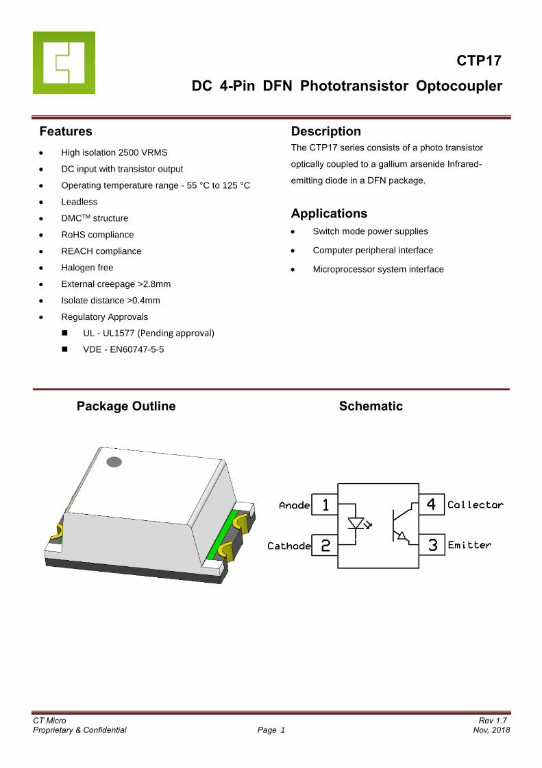
Package Outline Schematic
Features
• High isolation 2500 VRMS
• DC input with transistor output
• Operating temperature range - 55 °C to 125 °C
• Leadless
• DMCTM structure
• RoHS compliance
• REACH compliance
• Halogen free
• External creepage >2.8mm
• Isolate distance >0.4mm
• Regulatory Approvals
◼ UL - UL1577 (Pending approval)
◼ VDE - EN60747-5-5
Description
The CTP17 series consists of a photo transistor
optically coupled to a gallium arsenide Infrared-
emitting diode in a DFN package.
Applications
• Switch mode power supplies
• Computer peripheral interface
• Microprocessor system interface
CT Micro Rev 1.7 Proprietary & Confidential Page 2 Nov, 2018
CTP17
DC 4-Pin DFN Phototransistor Optocoupler
Absolute Maximum Rating at 25oC
Symbol Parameters Ratings Units Notes
VISO Isolation voltage 2500 VRMS
PTOT Total power dissipation 135 mW
TOPR Operating temperature -55 ~ +125 oC
TSTG Storage temperature -55 ~ +150 oC
TSOL Soldering temperature 260 oC
Emitter
IF Forward current 20 mA
IF(TRANS) Peak transient current (≤1μs P.W,300pps) 100 mA
VR Reverse voltage 6 V
PD Emitter power dissipation 35 mW
Detector
PC Detector power dissipation 100 mW
BVCEO Collector-Emitter Breakdown Voltage 80 V
BVECO Emitter-Collector Breakdown Voltage 7 V
IC Collector Current 50 mA
CT Micro Rev 1.7 Proprietary & Confidential Page 3 Nov, 2018
CTP17
DC 4-Pin DFN Phototransistor Optocoupler
Electrical Characteristics TA = 25°C (unless otherwise specified)
Emitter Characteristics
Symbol Parameters Test Conditions Min Typ Max Units Notes
VF Forward voltage IF=10mA - 1.25 1.4 V
IR Reverse Current VR = 6V - - 5 µA
CIN Input Capacitance f= 1MHz - 10 30 pF
Detector Characteristics
Symbol Parameters Test Conditions Min Typ Max Units Notes
BVCEO Collector-Emitter Breakdown IC= 100µA 80 - - V
BVECO Emitter-Collector Breakdown IEC= 100µA 7 - - V
ICEO Collector-Emitter Dark Current VCE= 40V, IF=0mA - - 100 nA
Transfer Characteristics
Symbol Parameters Test Conditions Min Typ Max Units Notes
CTR Current Transfer Ratio IF= 1mA, VCE= 5V
CTP17 100 - 600
%
1
CTP17B 100 - 300
CTP17C 200 - 400
CTP17D 300 - 600
CTR Current Transfer Ratio IF= 1mA, VCE= 0.4V 50 - - %
VCE(SAT) Collector-Emitter Saturation
Voltage IF= 1mA, IC= 0.5mA - 0.2 0.4 V
RIO Isolation Resistance VIO= 500VDC 5x10¹⁰ - - Ω
CIO Isolation Capacitance f= 1MHz - 0.25 1 pF
Switching Characteristics
Symbol Parameters Test Conditions Min Typ Max Units Notes
tr Rise Time
IC= 2mA, VCE= 2V
RL= 100Ω
- 5 16 µs
tf Fall Time - 6 16
ton Turn-on time - 8 20 µs
toff Turn-off time - 7 20
Note1:CTP17 is random shipment
CT Micro Rev 1.7 Proprietary & Confidential Page 4 Nov, 2018
CTP17
DC 4-Pin DFN Phototransistor Optocoupler
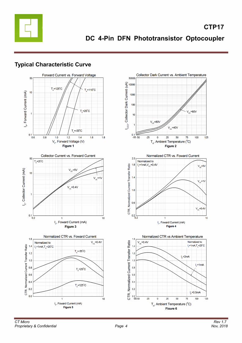
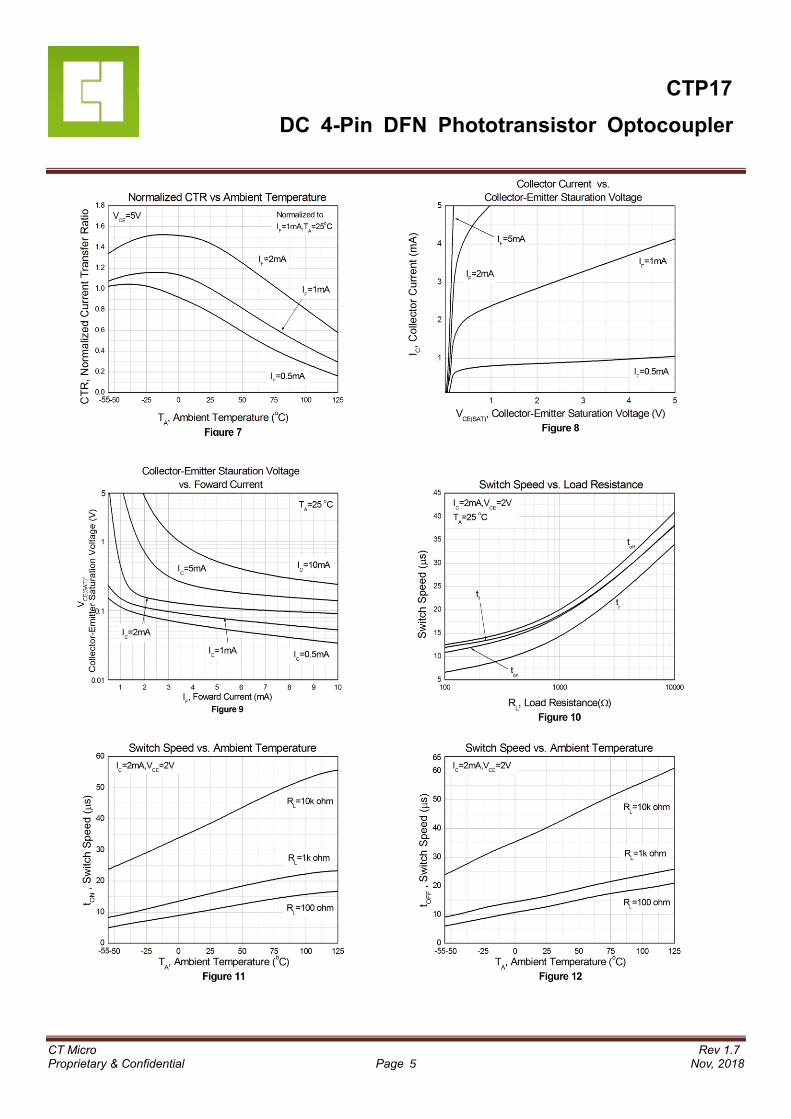
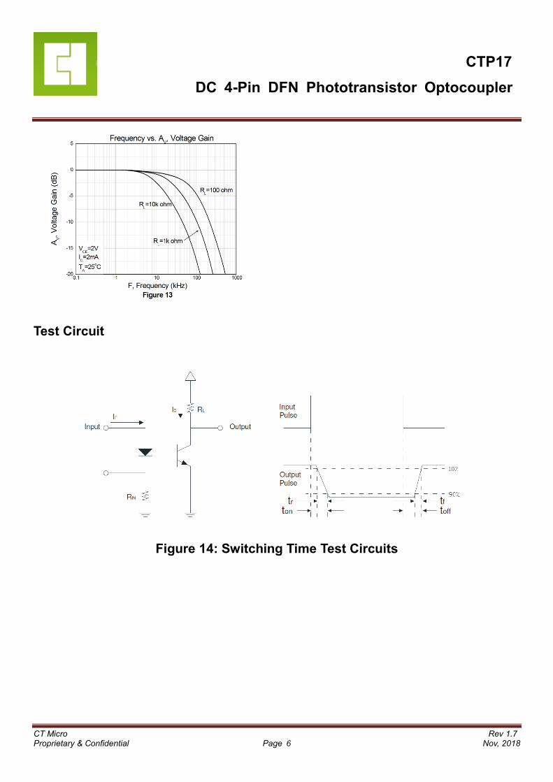
Typical Characteristic Curve
CT Micro Rev 1.7 Proprietary & Confidential Page 5 Nov, 2018
CTP17
DC 4-Pin DFN Phototransistor Optocoupler
CT Micro Rev 1.7 Proprietary & Confidential Page 6 Nov, 2018
CTP17
DC 4-Pin DFN Phototransistor Optocoupler
Test Circuit
Figure 14: Switching Time Test Circuits
CT Micro Rev 1.7 Proprietary & Confidential Page 7 Nov, 2018
CTP17
DC 4-Pin DFN Phototransistor Optocoupler
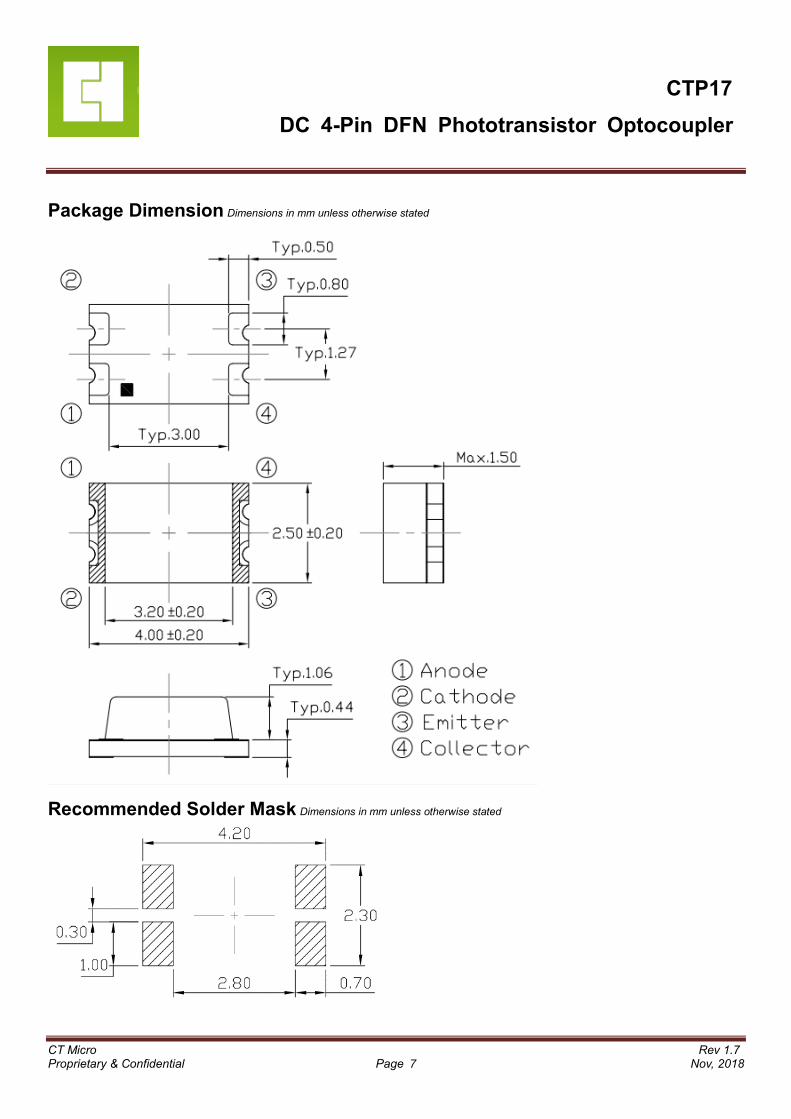
Package Dimension Dimensions in mm unless otherwise stated
Recommended Solder Mask Dimensions in mm unless otherwise stated
CT Micro Rev 1.7 Proprietary & Confidential Page 8 Nov, 2018
CTP17
DC 4-Pin DFN Phototransistor Optocoupler
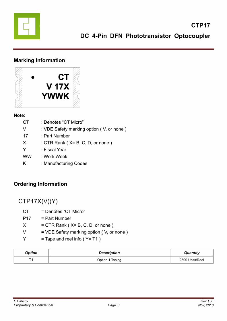
Marking Information
Note:
CT : Denotes “CT Micro”
V : VDE Safety marking option ( V, or none )
17 : Part Number
X : CTR Rank ( X= B, C, D, or none )
Y : Fiscal Year
WW : Work Week
K : Manufacturing Codes
Ordering Information
CTP17X(V)(Y)
CT = Denotes “CT Micro”
P17 = Part Number
X = CTR Rank ( X= B, C, D, or none )
V = VDE Safety marking option ( V, or none )
Y = Tape and reel info ( Y= T1 )
Option Description Quantity
T1 Option 1 Taping 2500 Units/Reel
․ CT V 17X
YWWK
CT Micro Rev 1.7 Proprietary & Confidential Page 9 Nov, 2018
CTP17
DC 4-Pin DFN Phototransistor Optocoupler
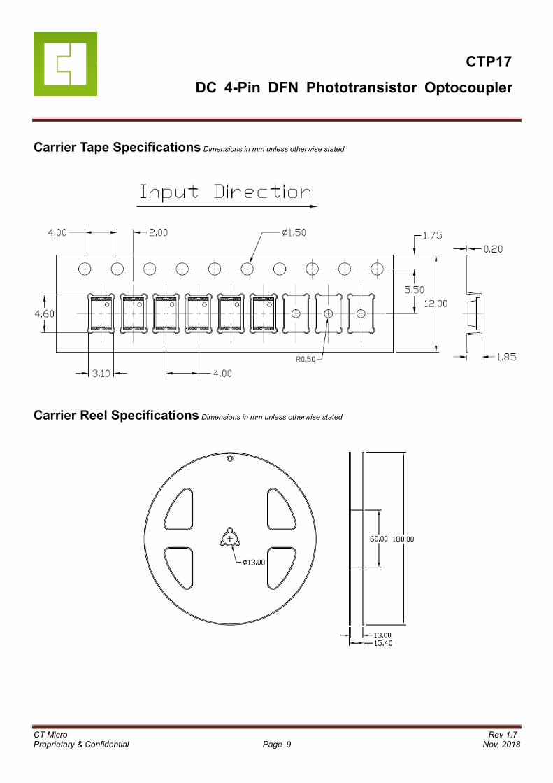
Carrier Tape Specifications Dimensions in mm unless otherwise stated
Carrier Reel Specifications Dimensions in mm unless otherwise stated
CT Micro Rev 1.7 Proprietary & Confidential Page 10 Nov, 2018
CTP17
DC 4-Pin DFN Phototransistor Optocoupler
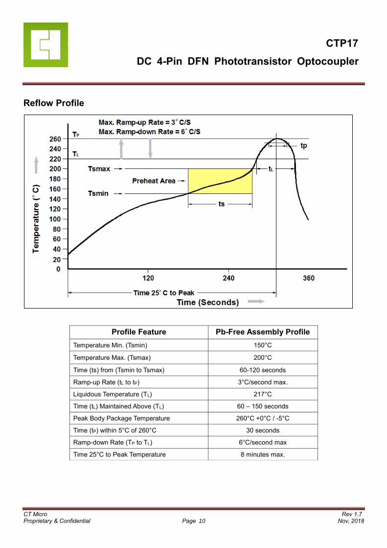
Reflow Profile
Profile Feature Pb-Free Assembly Profile
Temperature Min. (Tsmin) 150°C
Temperature Max. (Tsmax) 200°C
Time (ts) from (Tsmin to Tsmax) 60-120 seconds
Ramp-up Rate (tL to tP) 3°C/second max.
Liquidous Temperature (TL) 217°C
Time (tL) Maintained Above (TL) 60 – 150 seconds
Peak Body Package Temperature 260°C +0°C / -5°C
Time (tP) within 5°C of 260°C 30 seconds
Ramp-down Rate (TP to TL) 6°C/second max
Time 25°C to Peak Temperature 8 minutes max.
CT Micro Rev 1.7 Proprietary & Confidential Page 11 Nov, 2018
CTP17
DC 4-Pin DFN Phototransistor Optocoupler
DISCLAIMER
CT MICRO RESERVES THE RIGHT TO MAKE CHANGES WITHOUT FURTHER NOTICE TO ANY PRODUCTS
HEREIN TO IMPROVE RELIABILITY, FUNCTION OR DESIGN. CT MICRO DOES NOT ASSUME ANY LIABILITY
ARISING OUT OF THE APPLICATION OR USE OF ANY PRODUCT OR CIRCUIT DESCRIBED HEREIN;
NEITHER DOES IT CONVEY ANY LICENSE UNDER ITS PATENT RIGHTS, NOR THE RIGHTS OF OTHERS.
______________________________________________________________________________________
DISCOLORATION MIGHT OCCUR ON THE PACKAGE SURFACE AFTER SOLDERING, REFLOW OR LONG
TERM USE. THIS DOES NOT IMPACT THE PRODUCT PERFORMANCE NOR THE PRODUCT RELIABILITY.
CT MICRO ARE NOT AUTHORIZED FOR USE AS CRITICAL COMPONENTS IN LIFE SUPPORT DEVICES OR
SYSTEMS WITHOUT EXPRESS WRITTEN APPROVAL OF CT MICRO INTERNATIONAL CORPORATION.
1. Life support devices or systems are devices or
systems which, (a) are intended for surgical
implant into the body, or (b) support or sustain life,
or (c) whose failure to perform when properly used
in accordance with instruction for use provided in
the labelling, can be reasonably expected to result
in significant injury to the user.
2. A critical component is any component of a life
support device or system whose failure to perform
can be reasonably expected to cause the failure of
the life support device or system, or to affect its
safety or effectiveness.