Embed Size (px)
Citation preview
CSE 352 Laboratory Assignment 1
Logistics / Constructing Simple Logic Circuits
Assigned: Oct. 4/6, 2011
Due: Beginning of Lab Section next week
Objectives
Read the whole lab first before starting on any work. This lab starts with the preliminaries; signing out your
lab kits and making sure you can log in to the lab computers and start the software you’ll be using this quarter.
We then introduce you to Altera’s Terasic DE1 prototyping board and our primary design tool this quarter -
both for schematic entry (drawing circuits) and simulating them (verifying that they will operate correctly when
we wire them up) - Aldec's Active- HDL. Both of these components are very important for all future labs so
please pay attention and do not rush through this first lab. Though we typically encourage you to work together,
it is recommended you do this lab individually to gain the full benefits of the lab.
In this assignment you will learn how to do both schematic entry and simulation for some basic circuits. As you
gain more practice with Active-HDL, we will expect you to use this tool to do a large part of your written
assignments throughout the quarter. This means, you will see Active-HDL assignments incorporated into your
homework, so don’t skimp on these labs, they’re important!
By the end of this lab you should feel comfortable entering a schematic for a design, setting up simulation
stimuli, and verifying that your circuit is correct. The overall goal for this lab will be to construct a circuit which
performs the Boolean combination you derive, of course the circuit will have to only use the chips provided for
you. By the end of this lab you should know how to construct and verify the operation of a small circuit (3-6
logic gates) in both Active-HDL and on your prototyping board using switches and LEDs as I/O devices.
If you have any questions at any point in the lab, make sure you have read the entire lab thoroughly, and ask a
TA if you still cannot find the answer. As always, there are no dumb questions, please ask your TAs; you want
to you don’t want to damage any of the expensive hardware that is provided for you.
This is a rather long lab since you are learning an entirely new design tool – Active-HDL. You can go through
the first two Active-HDL tutorials before you get to lab and start working with the design kits.
Laboratory Design Kits
The design kits contain everything you need to construct most of the circuits assigned to you over the course of
the quarter. You are responsible for your lab kit and we expect that you will return the kit in good working order
with all pieces intact. This especially applies to the chips, which have very delicate pins (that should inserted
and removed from the solder-less bread-board – the white rectangle will all the holes – with extra care).
Altera Terasic DE1 Protoyping Board
A solder-less bread board attached to the prototyping board,
and the Input/Output Connectors attached to the prototyping board.
A power supply, or a USB cable that will be used to power your prototyping board
A Logic Probe
A Wire Stripper/Cutter
Needle-Nosed Pliers
A Set of Provided TTL Logic Chips. All of these chips are Dual-In-Line Packages and are compatible
with your breadboard.
Chip Extractor Tool (This is the tool you should use to evenly remove chips from the breadboard. Don't
use your fingers to pry up the chips because it could snap the pins or you could injure yourself on the
tips of the pins
Please make sure all of the above are provided for you in your kit. We will provide additional materials later on
in the quarter if they are necessary to complete a lab.
We are aware that accidents can happen and the pins on chips may already been weakened from years of use.
Typically if you break a pin the chip will be replaced and the damage will be forgiven; however in cases of
gross negligence you will have to pay for a replacement. Take care not to short out your board by connecting
Ground to Power. This results in a very large current that can quickly destroy the components of the board
including the board itself. Finally be careful not to snap off wires inside the I/O connectors or the holes in the
solder-less breadboard. Wires are best extracted with the needle-nosed pliers.
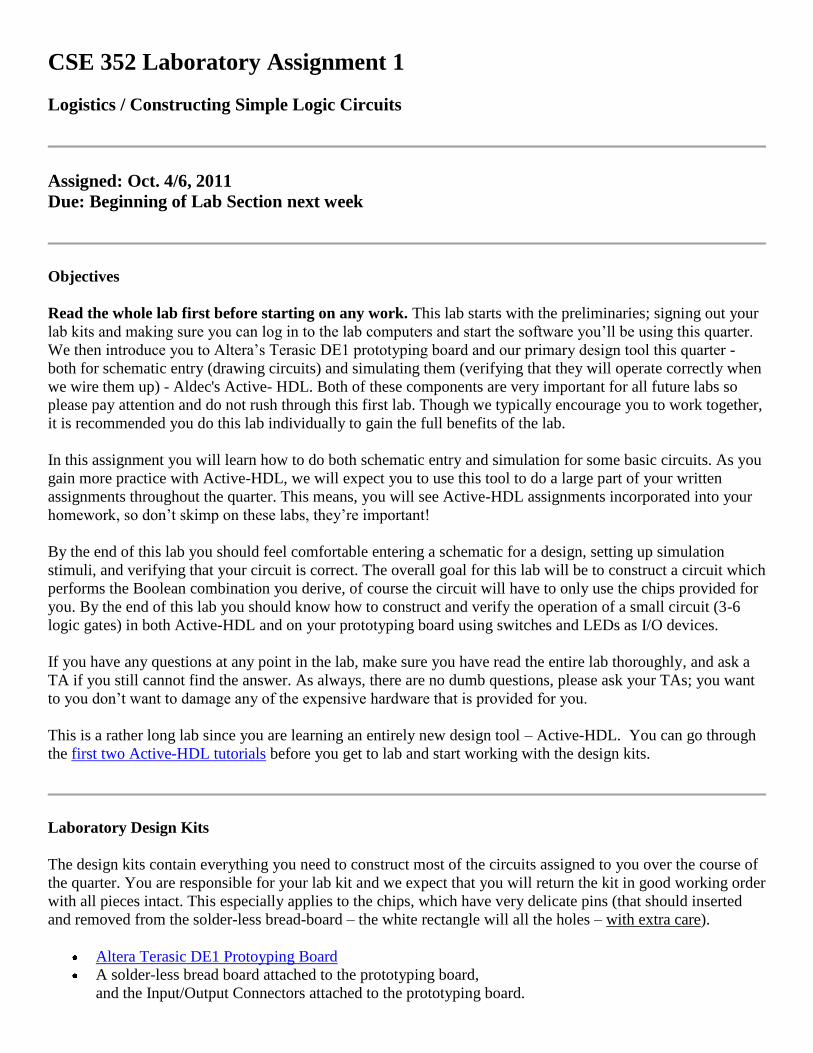
Altera Terasic DE1 Prototyping Board
The picture above is a diagram of the prototyping board with most of the major components highlighted. For the
first few labs you will be using the various input/output devices located directly on the board such as the
switches and LEDs. Further details will be provided in each lab. Take note of the large FPGA (Field
Programmable Gate Array) that is highlighted on the board. Later on in the quarter you will be programming
this and directly interfacing with all the devices on the board.
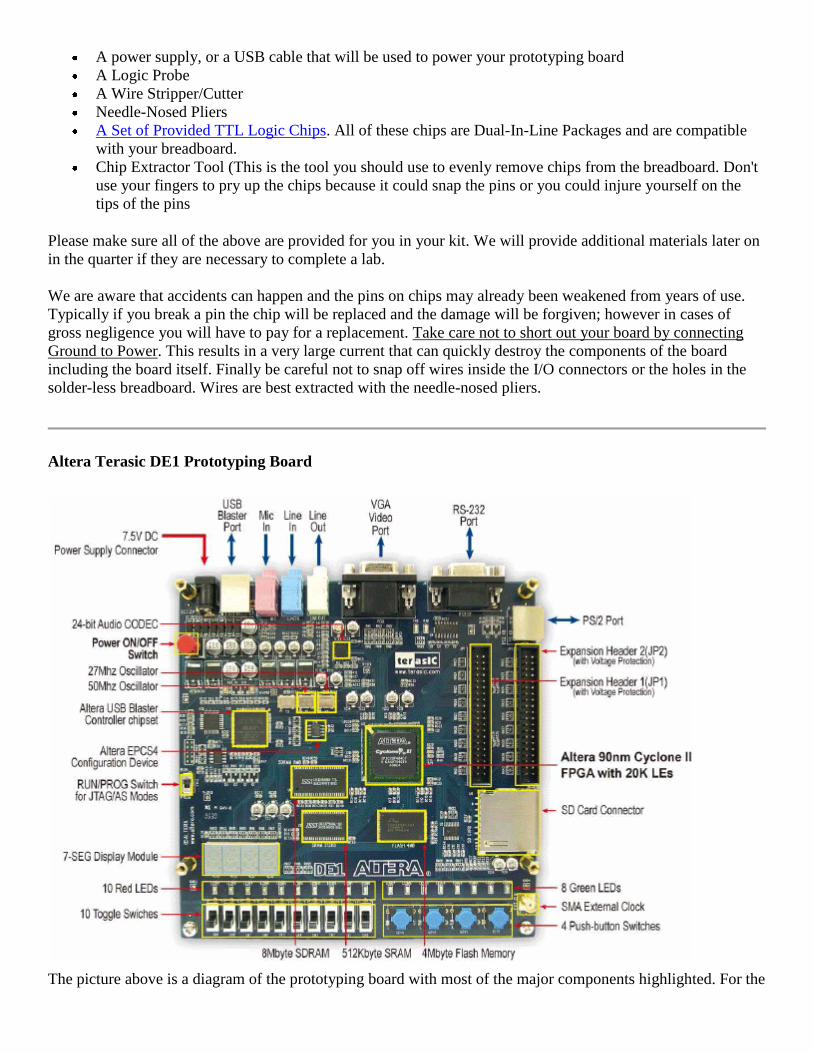
Switches, Keys, and LEDs
The image is a zoomed in picture of the prototyping board. As you can see, each little hole has a corresponding
pin mapping (more on this in later labs) and a pre-programmed functionality. Remember the program that the
TA’s put in the non-volatile memory mentioned above? Well in addition to having the HEX display scroll CSE
370, the program also maps those holes to the indicated switches, keys, or LEDs. So for example, if I hooked up
the hole labeled "A13 SW9" to the hole labeled "D21 LEDR9" with a wire, I would be controlling the red led
labeled LEDR9 on the DE1 board with the switch labeled SW9.
The FPGA
An FPGA is short for Field Programmable Gate Array. Essentially it is a large array of logical elements that
have been connected together. What makes the FPGA unique is that the connections between these logical
elements can be programmed, which means the FPGA can be used to build many different kinds of hardware all
on the same chip. If you look at the HEX display on the bottom left hand corner of your DE1 board you will see
that it has a scrolling message which says CSE 370. This is a program that the TAs have written and
programmed into your FPGA’s non-volatile memory. By programming into the non-volatile memory, each time
the board is turned on the CSE 370 program will be loaded, regardless of what you did previously.
The Solder-Less Bread Board
The solder-less breadboard attached to your prototyping board is where you will be building all of your circuits.
Notice the red and black wires going to each of the rows at the top and bottom of the board. The red wire
denotes VDD (+5 Volts) and the black wire denotes Ground (0 Volts) – we will always use this convention with
all our circuits. Never directly connect these two rows together in any way. You should have both a VDD and
Ground at the top of your board and a set at the bottom. Even though there are spaces between the rows all of
the holes are directly connected to each other. This means you have rails of VDD and Ground both at the top
and bottom of your board.
In addition to the rails of VDD and Ground provided for you on the board there are two 43 column holes
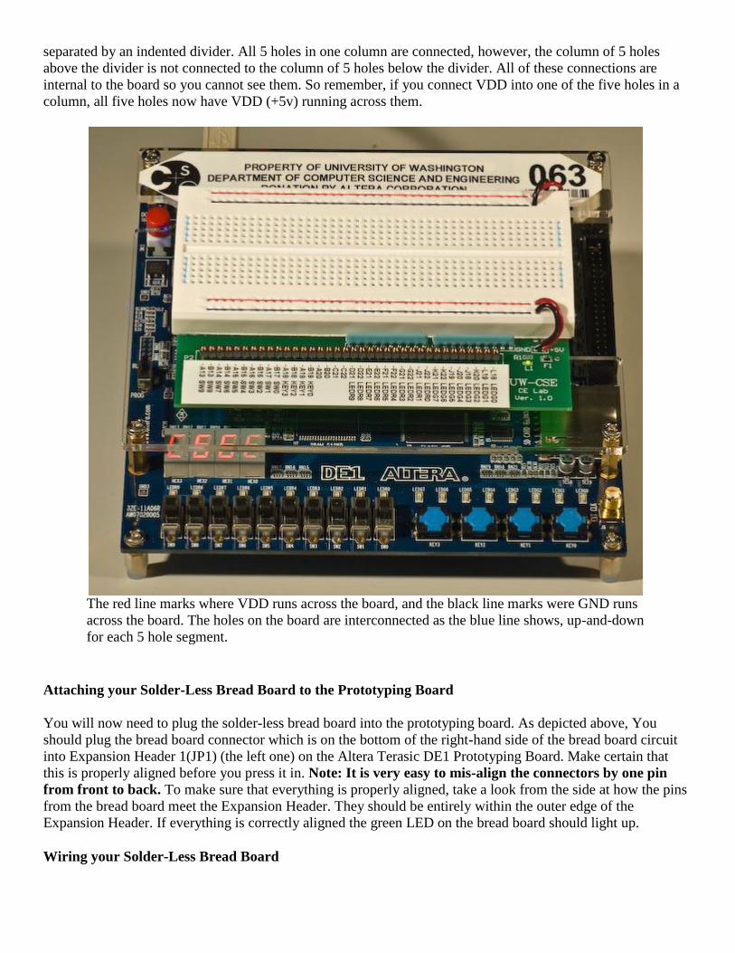
separated by an indented divider. All 5 holes in one column are connected, however, the column of 5 holes
above the divider is not connected to the column of 5 holes below the divider. All of these connections are
internal to the board so you cannot see them. So remember, if you connect VDD into one of the five holes in a
column, all five holes now have VDD (+5v) running across them.
The red line marks where VDD runs across the board, and the black line marks were GND runs
across the board. The holes on the board are interconnected as the blue line shows, up-and-down
for each 5 hole segment.
Attaching your Solder-Less Bread Board to the Prototyping Board
You will now need to plug the solder-less bread board into the prototyping board. As depicted above, You
should plug the bread board connector which is on the bottom of the right-hand side of the bread board circuit
into Expansion Header 1(JP1) (the left one) on the Altera Terasic DE1 Prototyping Board. Make certain that
this is properly aligned before you press it in. Note: It is very easy to mis-align the connectors by one pin
from front to back. To make sure that everything is properly aligned, take a look from the side at how the pins
from the bread board meet the Expansion Header. They should be entirely within the outer edge of the
Expansion Header. If everything is correctly aligned the green LED on the bread board should light up.
Wiring your Solder-Less Bread Board

Wires should be inserted as perpendicular as possible to the breadboard and should slide in and out with just a
little force. If you find that there is a lot of resistance in either direction, first review the wiring guidelines
below, and if that doesn't work, then please call over the TA or one of the lab staff.
Do not try to force anything larger than stripped wires into the holes, because this could damage the bread board
(at great cost). If you need more wire help yourself to the provided spools of uncut wire at the front of the lab.
Before doing any work on the bread board such as wiring and inserting/removing chips, be sure the power is
OFF. That is, unplug the power connector while you are constructing the circuit. After you have finished wiring
up your design and before you turn on the power, double check the power and ground connections.
Wiring Guidelines
Wiring your circuit together can often feel tedious, especially in the beginning. However, if you are patient and
wire your circuit nicely, you will find that you will spend a lot less time tracking down wiring errors. To aid you
in this, here are a few tips to consider while wiring up your circuit. If anything is unclear, ask your TA for an
example.
Make sure your wires are stripped nicely. This means that when you put the wire in your bread board,
there shouldn't be any un-insulated wire visible and the wire shouldn't crunch against the bottom of the
board.
Your wires should always be nice and straight, there should be no twists or kinks in it, as they can cause
your board to short out when you insert them in your bread board.
Arrange the chips on the bread board so that only short wire connections are needed. Put tightly
connected chips closer together. Chips will only fit with one set of pins on one side of the center divider
and another set of pins on the other side of the divider.
Do not make a jungle of wires. Long looping wires that go way into the air are easy to pull out (a hard
bug to find later when the circuit doesn't work as intended).
Try to maintain a low wiring profile so that you can reach the pins of the chips and so the chips can be
replaced if necessary. The best connections are those that lie flat on the board. Try to avoid wiring over
any chips so that chips can be removed easily and replaced.
For those of you that learn better by seeing, here is a good wiring example and a bad wiring example.
Using the Logic Probe
The logic probe provides a very convenient way to check the value of any signal in your circuit. The probe has
two lights, HI and LO, which indicate the value of the signal. The logic probe responds to the input voltage in
two ways depending on whether CMOS or TTL is selected. We will use the TTL setting which lights the LO
(Logical 0) light for voltages <0.8v. and lights the HI (Logical 1) light for voltages >2.3v. If neither light is lit,
then the signal is floating (i.e. not being driven by any active output) or has some value between 0.8 and 2.3v.
Duplicating NOT Gate Behavior
Read This, this can simplify later labs. Now that you have begun to use NOT and NOR gates, did you know
there are ways to duplicate the behavior of a NOT gate with a NOR or NAND gate? Consider the two logic
tables below: Notice what happens when drive both the inputs of a NOR gate with the same output, it acts like a
NOT gate. The same applies for an NAND gate, when you drive both of the inputs of a NAND gate with the
same signal it acts like a NOT gate as well. Now if you are short an inverter, but you have NANDs and NORs
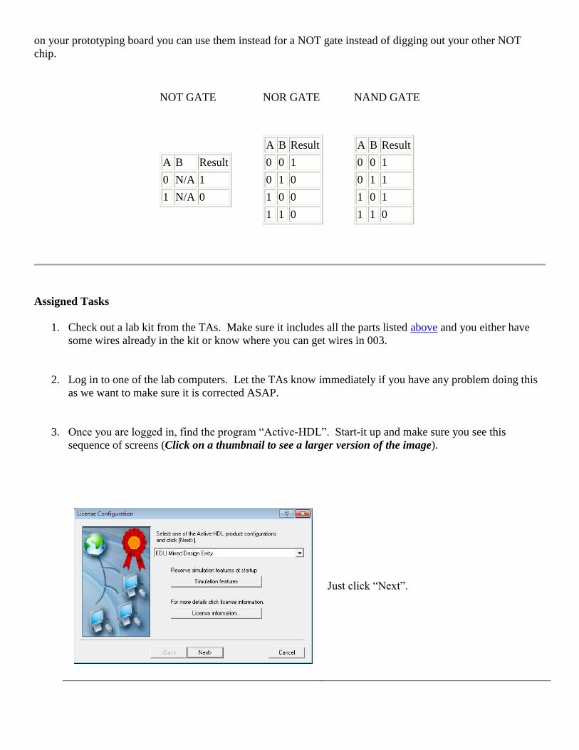
on your prototyping board you can use them instead for a NOT gate instead of digging out your other NOT
chip.
NOT GATE NOR GATE NAND GATE
A B Result
0 N/A 1
1 N/A 0
A B Result
0 0 1
0 1 0
1 0 0
1 1 0
A B Result
0 0 1
0 1 1
1 0 1
1 1 0
Assigned Tasks
1. Check out a lab kit from the TAs. Make sure it includes all the parts listed above and you either have
some wires already in the kit or know where you can get wires in 003.
2. Log in to one of the lab computers. Let the TAs know immediately if you have any problem doing this
as we want to make sure it is corrected ASAP.
3. Once you are logged in, find the program “Active-HDL”. Start-it up and make sure you see this
sequence of screens (Click on a thumbnail to see a larger version of the image).
Just click “Next”.
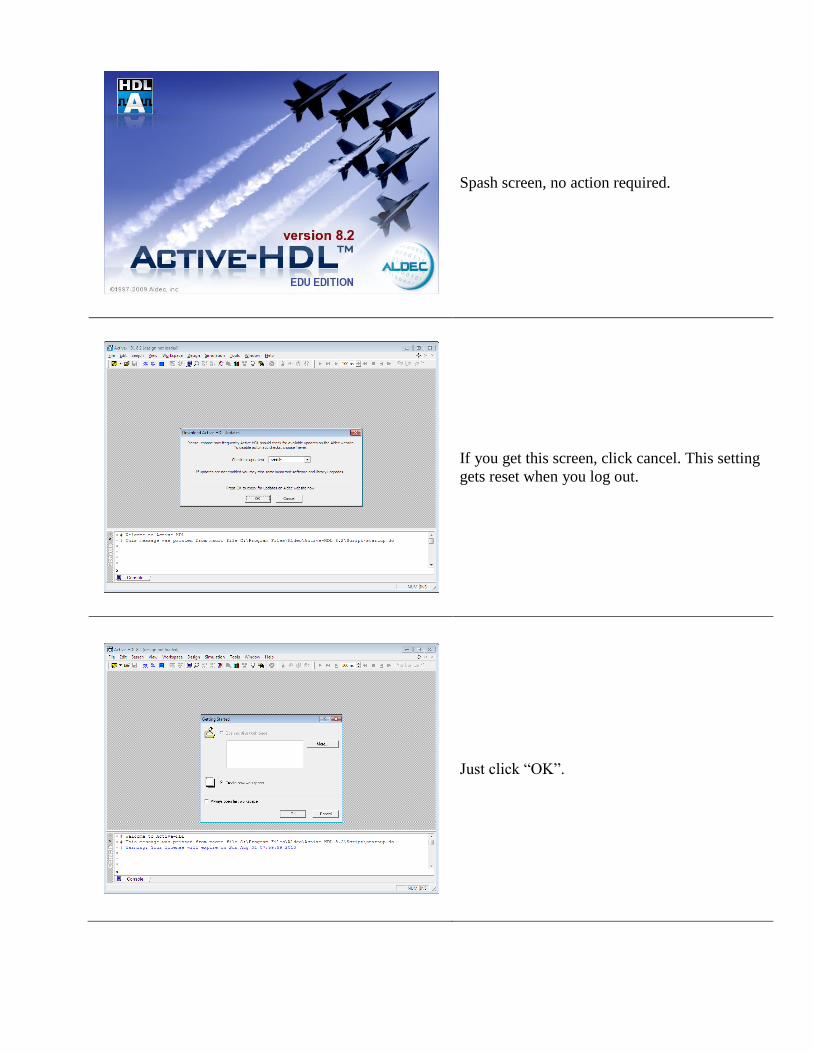
Spash screen, no action required.
If you get this screen, click cancel. This setting
gets reset when you log out.
Just click “OK”.
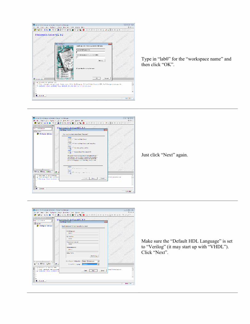
Type in “lab0” for the “workspace name” and
then click “OK”.
Just click “Next” again.
Make sure the “Default HDL Language” is set
to “Verilog” (it may start up with “VHDL”).
Click “Next”.
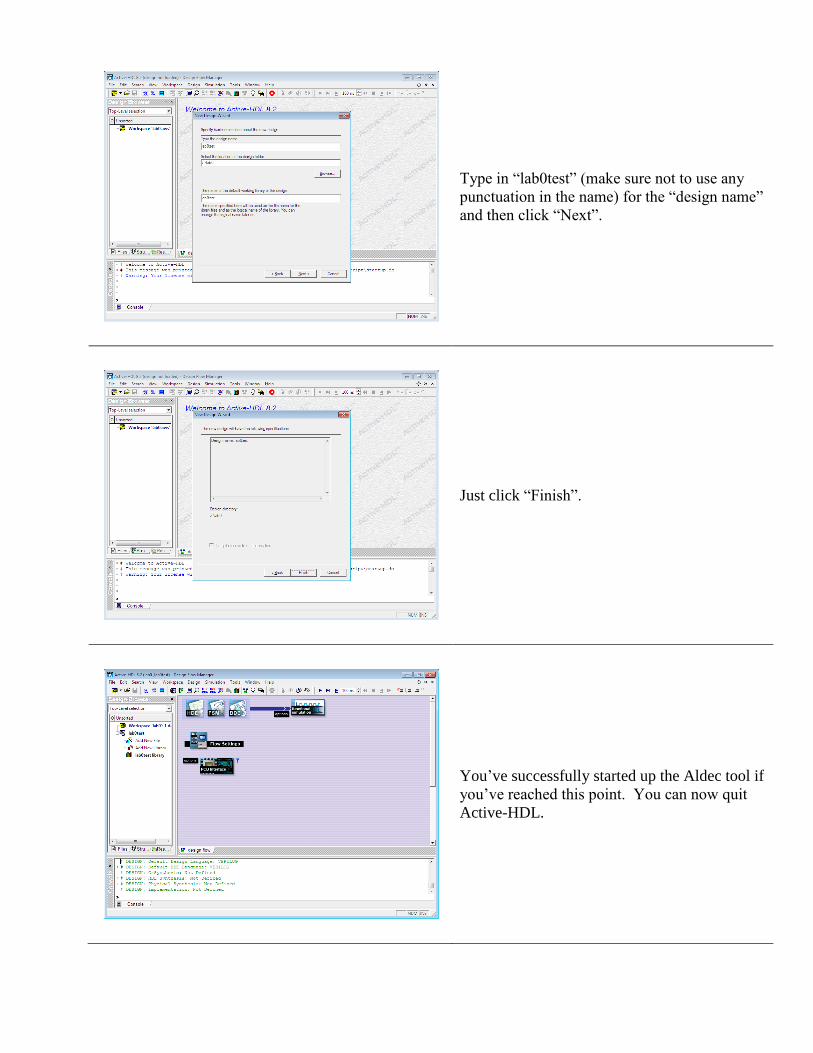
Type in “lab0test” (make sure not to use any
punctuation in the name) for the “design name”
and then click “Next”.
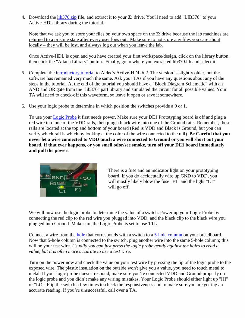
Just click “Finish”.
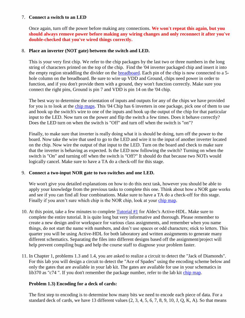
You’ve successfully started up the Aldec tool if
you’ve reached this point. You can now quit
Active-HDL.
4. Download the lib370.zip file, and extract it to your Z: drive. You'll need to add "LIB370" to your
Active-HDL library during the tutorial.
Note that we ask you to store your files on your own space on the Z: drive because the lab machines are
returned to a pristine state after every user logs out. Make sure to not store any files you care about
locally – they will be lost, and always log out when you leave the lab.
Once Active-HDL is open and you have created your first workspace/design, click on the library button,
then click the "Attach Library" button. Finally, go to where you extracted lib370.lib and select it.
5. Complete the introductory tutorial to Aldec's Active-HDL 6.2. The version is slightly older, but the
software has remained very much the same. Ask your TAs if you have any questions about any of the
steps in the tutorial. At the end of the tutorial you should have a "Block Diagram Schematic" with an
AND and OR gate from the "lib370" part library and simulated the circuit for all possible values. Your
TA will need to check-off this waveform, so leave it open or save it somewhere.
6. Use your logic probe to determine in which position the switches provide a 0 or 1.
To use your Logic Probe it first needs power. Make sure your DE1 Prototyping board is off and plug a
red wire into one of the VDD rails, then plug a black wire into one of the Ground rails. Remember, these
rails are located at the top and bottom of your board (Red is VDD and Black is Ground, but you can
verify which rail is which by looking at the color of the wire connected to the rail). Be Careful that you
never let a wire connected to VDD touch a wire connected to Ground or you will short out your
board. If that ever happens, or you smell odor/see smoke, turn off your DE1 board immediately
and pull the power.
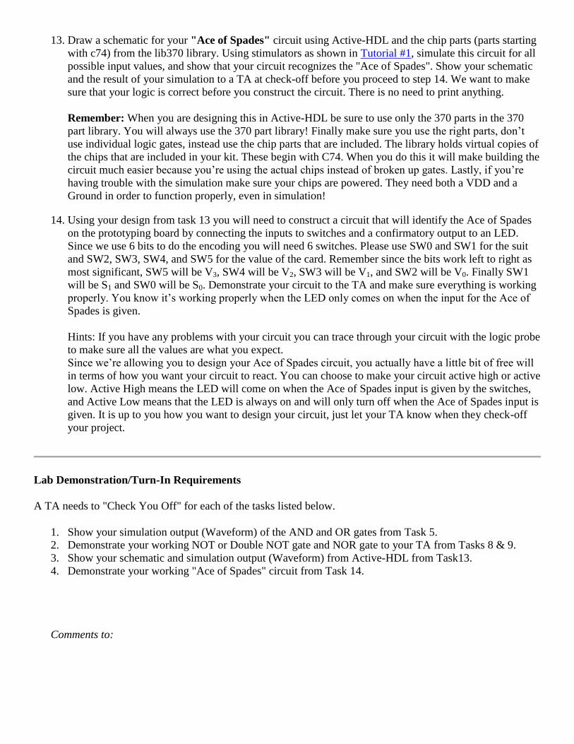
There is a fuse and an indicator light on your prototyping
board. If you do accidentally wire up GND to VDD, you
will mostly likely blow the fuse "F1" and the light "L1"
will go off.
We will now use the logic probe to determine the value of a switch. Power up your Logic Probe by
connecting the red clip to the red wire you plugged into VDD, and the black clip to the black wire you
plugged into Ground. Make sure the Logic Probe is set to use TTL.
Connect a wire from the hole that corresponds with a switch to a 5-hole column on your breadboard.
Now that 5-hole column is connected to the switch, plug another wire into the same 5-hole column; this
will be your test wire. Usually you can just press the logic probe gently against the holes to read a
value, but it is often more accurate to use a test wire.
Turn on the power now and check the value on your test wire by pressing the tip of the logic probe to the
exposed wire. The plastic insulation on the outside won't give you a value, you need to touch metal to
metal. If your logic probe doesn't respond, make sure you’re connected VDD and Ground properly on
the logic probe and you didn’t make any wiring mistakes. Your Logic Probe should either light up "HI"
or "LO". Flip the switch a few times to check the responsiveness and to make sure you are getting an
accurate reading. If you’re unsuccessful, call over a TA.
7. Connect a switch to an LED
Once again, turn off the power before making any connections. We won't repeat this again, but you
should always remove power before making any wiring changes and only reconnect it after you've
double-checked that you've wired things correctly.
8. Place an inverter (NOT gate) between the switch and LED.
This is your very first chip. We refer to the chip packages by the last two or three numbers in the long
string of characters printed on the top of the chip. Find the '04 inverter packaged chip and insert it into
the empty region straddling the divider on the breadboard. Each pin of the chip is now connected to a 5-
hole column on the breadboard. Be sure to wire up VDD and Ground, chips need power in order to
function, and if you don't provide them with a ground, they won't function correctly. Make sure you
connect the right pins, Ground is pin 7 and VDD is pin 14 on the '04 chip.
The best way to determine the orientation of inputs and outputs for any of the chips we have provided
for you is to look at the chip maps. This '04 Chip has 6 inverters in one package, pick one of them to use
and hook up the switch's wire to one of the inputs and hook up the output of the chip for that particular
input to the LED. Now turn on the power and flip the switch a few times. Does it behave correctly?
Does the LED turn on when the switch is "Off" and turn off when the switch is "on"?
Finally, to make sure that inverter is really doing what it is should be doing, turn off the power to the
board. Now take the wire that used to go to the LED and wire it to the input of another inverter located
on the chip. Now wire the output of that input to the LED. Turn on the board and check to make sure
that the inverter is behaving as expected. Is the LED now following the switch? Turning on when the
switch is "On" and turning off when the switch is "Off?" It should do that because two NOTs would
logically cancel. Make sure to have a TA do a check-off for this stage.
9. Connect a two-input NOR gate to two switches and one LED.
We won't give you detailed explanations on how to do this next task, however you should be able to
apply your knowledge from the previous tasks to complete this one. Think about how a NOR gate works
and see if you can find all four combinations. Make sure to have a TA do a check-off for this stage.
Finally if you aren’t sure which chip is the NOR chip, look at your chip map.
10. At this point, take a few minutes to complete Tutorial #1 for Aldec's Active-HDL. Make sure to
complete the entire tutorial. It is quite long but very informative and thorough. Please remember to
create a new design and/or workspace for various class assignments, and remember when you name
things, do not start the name with numbers, and don’t use spaces or odd characters; stick to letters. This
quarter you will be using Active-HDL for both laboratory and written assignments to generate many
different schematics. Separating the files into different designs based off the assignment/project will
help prevent compiling bugs and help the course staff to diagnose your problem faster.
11. In Chapter 1, problems 1.3 and 1.4, you are asked to realize a circuit to detect the "Jack of Diamonds".
For this lab you will design a circuit to detect the "Ace of Spades" using the encoding scheme below and
only the gates that are available in your lab kit. The gates are available for use in your schematics in
lib370 as "c74 ". If you don't remember the package number, refer to the lab kit chip map.
Problem 1.3) Encoding for a deck of cards:
The first step to encoding is to determine how many bits we need to encode each piece of data. For a
standard deck of cards, we have 13 different values (2, 3, 4, 5, 6, 7, 8, 9, 10, J, Q, K, A). So that means

we need at least 4 bits to represent the 13 different values. Since two to the forth power gives 16, which
is more than 13 so 4 bits should be enough. Finally we have 4 different suits, (Clubs, Diamonds, Hearts,
and Spades), which means we’ll need 2 bits; since two to the second power is 4, to represent the suits.
So the value 0 will be assigned to clubs, 1 to diamonds, 2 to hearts, and 3 to spades. This means we’ll
need a total of 6 bits to encode an entire standard deck of cards.
We’ll be using a specific encoding, so make sure you follow it when you do this lab assignment. First
off, we won’t be using the values of 0, 14, and 15. Finally the encoding will done in the following order:
V3V2 V1 V0 S1 S 0
In general, note that the higher-numbered subscripts denote higher- order (more significant) bits. By
convention, bits progress, left to right, from most significant to least significant. So now, the encoding is
as follows in table form:
Value/Decimal Value Binary Encoding
Ace / 1 0001
2 / 2 0010
3 / 3 0011
4 / 4 0100
5 / 5 0101
6 / 6 0110
7 / 7 0111
8 / 8 1000
9 / 9 1001
10 / 10 1010
Jack / 11 1011
Queen / 12 1100
King / 13 1101
Suit/Value Binary Encoding
Clubs / 0 00
Diamonds / 1 01
Hearts / 2 10
Spaces / 3 11
12. Problem 1.4) An Example Encoding
As an example for the encoding above we’ll encode Jack of Diamonds. Remember, your assignment is
the Ace of Spades, so don’t build the Jack of Diamonds! So first off we look at the value of the card,
Jack corresponds to the value of 11, which means the encoding for the value should be 1011. Next the
suit is Diamond, which means the encoding should be 01. So if we put it all together in the format
described above we get: 1011_01. This can be represented as:
V3 and V2' and V1 and V0 and S1' and S0
You will have to design a circuit that will light up a light when the values for the Ace of Spades is
entered via the switches, one switch for each bit. Since you have to use only the chips provided make
sure your design uses NAND and/or NOR gates since your lab kit does not have AND gates. And
remember, the smaller and more efficient the circuit, the easier it is to debug and build!
13. Draw a schematic for your "Ace of Spades" circuit using Active-HDL and the chip parts (parts starting
with c74) from the lib370 library. Using stimulators as shown in Tutorial #1, simulate this circuit for all
possible input values, and show that your circuit recognizes the "Ace of Spades". Show your schematic
and the result of your simulation to a TA at check-off before you proceed to step 14. We want to make
sure that your logic is correct before you construct the circuit. There is no need to print anything.
Remember: When you are designing this in Active-HDL be sure to use only the 370 parts in the 370
part library. You will always use the 370 part library! Finally make sure you use the right parts, don’t
use individual logic gates, instead use the chip parts that are included. The library holds virtual copies of
the chips that are included in your kit. These begin with C74. When you do this it will make building the
circuit much easier because you’re using the actual chips instead of broken up gates. Lastly, if you’re
having trouble with the simulation make sure your chips are powered. They need both a VDD and a
Ground in order to function properly, even in simulation!
14. Using your design from task 13 you will need to construct a circuit that will identify the Ace of Spades
on the prototyping board by connecting the inputs to switches and a confirmatory output to an LED.
Since we use 6 bits to do the encoding you will need 6 switches. Please use SW0 and SW1 for the suit
and SW2, SW3, SW4, and SW5 for the value of the card. Remember since the bits work left to right as
most significant, SW5 will be V3, SW4 will be V2, SW3 will be V1, and SW2 will be V0. Finally SW1
will be S1 and SW0 will be S0. Demonstrate your circuit to the TA and make sure everything is working
properly. You know it’s working properly when the LED only comes on when the input for the Ace of
Spades is given.
Hints: If you have any problems with your circuit you can trace through your circuit with the logic probe
to make sure all the values are what you expect.
Since we’re allowing you to design your Ace of Spades circuit, you actually have a little bit of free will
in terms of how you want your circuit to react. You can choose to make your circuit active high or active
low. Active High means the LED will come on when the Ace of Spades input is given by the switches,
and Active Low means that the LED is always on and will only turn off when the Ace of Spades input is
given. It is up to you how you want to design your circuit, just let your TA know when they check-off
your project.
Lab Demonstration/Turn-In Requirements
A TA needs to "Check You Off" for each of the tasks listed below.
1. Show your simulation output (Waveform) of the AND and OR gates from Task 5.
2. Demonstrate your working NOT or Double NOT gate and NOR gate to your TA from Tasks 8 & 9.
3. Show your schematic and simulation output (Waveform) from Active-HDL from Task13.
4. Demonstrate your working "Ace of Spades" circuit from Task 14.
Comments to: