Embed Size (px)
Citation preview

CSC258 Week 1
1

Today’s outline
§ WhyCSC258§ What is in CSC258§ How to do well in CSC258
§ Start learning
3

Why takeCSC258?
4

Learning the Magic
5
magic magic
CSC258 CSC369

More specifically…
§ How do we express 1’s and 0’s using a piece of silicon?
§ How does the computer do everything with just 1’s and 0’s?
§ What is stored in that “fortnite.exe” file, what exactly happens when I double-click on it?
§ How does the CPU run an if-statement, or for loop, or recursion?
CSC258 has all the answers!
6

After learning CSC258…
§ You’ll know everything about how a computer is physically built, and you can build one if you want.
§ Base on your hardware knowledge, you will be able to engineer the performance of your software like never before.
7
People who are really serious about software should make their own hardware.
-- Alan Kay

What’s inCSC258?
8

The architecture of a computer hardware, level by level, bottom-up
Assembly Language
Processors
Finite State Machines
Arithmetic Logic Units
Devices Flip-flops
Circuits
Gates
Transistors
compute stuffremember stuff
9

We learn the whole real deal
§ From atom level to assembly level§ Above the assembly level is the Operating System,
whose main job is virtualization, i.e., create convenient illusions.
§ Everything you learn from every CS course are all illusions except for CSC258
10

How to do well in CSC258
11

First of all …
Be interested
12

Course website
http://www.cs.toronto.edu/~ylzhang/csc258/
All course materials are here.
13

Marking scheme
§ Labs: 3% x 10 = 30%§ Midterm: 22%§ Final exam: 45%§ Quizzes: 3%
100%
14

Labs (starting from Week 2)
§ Hands-on exercises in which you will build real pieces of hardware.
§ Prelabs are done individually, in-lab work is done in pairs.
§ ONLY go to the lab section that you are registered to on ACORN. If you want to switch lab section, find someone who is willing to switch and let Larry know.
§ On the discussion board, use “Search Teammates” for finding a partner.
15

Prelab Reports
§ For most of the labs, you will be required to submit a prelab report (a PDF file) to MarkUs before the labs start.
§ Must be completed individually
§ Submission deadline is typically Tuesday 3pm
§ To get the mark for the prelab report
ú do your work and submit something meaningful
ú don’t plagiarize
ú not submitting anything would be much better than plagiarizing
16

17

Lab software
§ We will use Logisim-Evolution§ The reference of the software has been posted on the course
website.§ Task for this week: download the software, read the reference,
and familiarize yourself with it.§ Note: I must be Logisim-Evolution downloaded at the link in
the reference. Do NOT use the original Logisim or its other variations.
18

Weekly Quizzes
§ We will use Quercus for online quizzes
§ Starting in Week 2
§ Useful practices for tests and exams.
§ Deadline for quizzes is every Sunday 10:00pm.
§ You’ll be told whether your answer is correct immediately, and you can try up to three times. We will record your highest score.
19

Tests!
§ Midterm§ out of class§ March 1, 5:10pm~6:40pm (90 minutes)§ Let Larry know by Jan 31 if you have a conflict.
§ Final exam§ Some time in April§ Must get >= 40%
20

Discussion board
https://mcs.utm.utoronto.ca/~mybb/utmcs2/forumdisplay.php?fid=32
§ All course announcements will be posted here.
§ Daily reading is required.
21

Office hours
Monday 5-6:30 pmTuesday 5-6:30 pm
22
Office hours are good.

Student Feedback
§ Give us frequently (e.g., every week) feedbacks on how things are going. It is very useful for improving your learning experience in a timely manner.
§ Anonymous feedback form:ú link on the course website
§ Or, just drop by and have a chat with Larry
2-23

Textbook: DDCA
Digital Design and Computer Architecture, 2nd edition, 2012by David Harris, Sarah Harris
Available online at UofTlibrary (link in course info sheet)
24

A typical week of CSC258
§ Monday/Tuesday: go the lectures.
§ By Tuesday 3pm: submit prelab report.
§ Tuesday/Wednesday/Thursday: labs.
§ Wednesday: Quiz out on Quercus, starting studying for it.
§ Thursday evening: next week’s lab handout released, start working on the prelab.
§ Sunday by 10pm: complete the quiz.
25

It will be a lot of work, and a lot of fun!
26

27

§ In-class pop quizzes. To participate, you’ll need:ú be in the lectureú have access to a browser (on a
phone, tablet or a laptop), or the Kahoot app
§ has nothing (directly) to do with your course grade
2-28

Let the learning begin
29

Basic Logic Gates
30

You already know something…
31

Logic from math course
§ Create an expression that is true iff the variables A and B are true, or C and D are true.
G = (A & B) | (C & D)
32
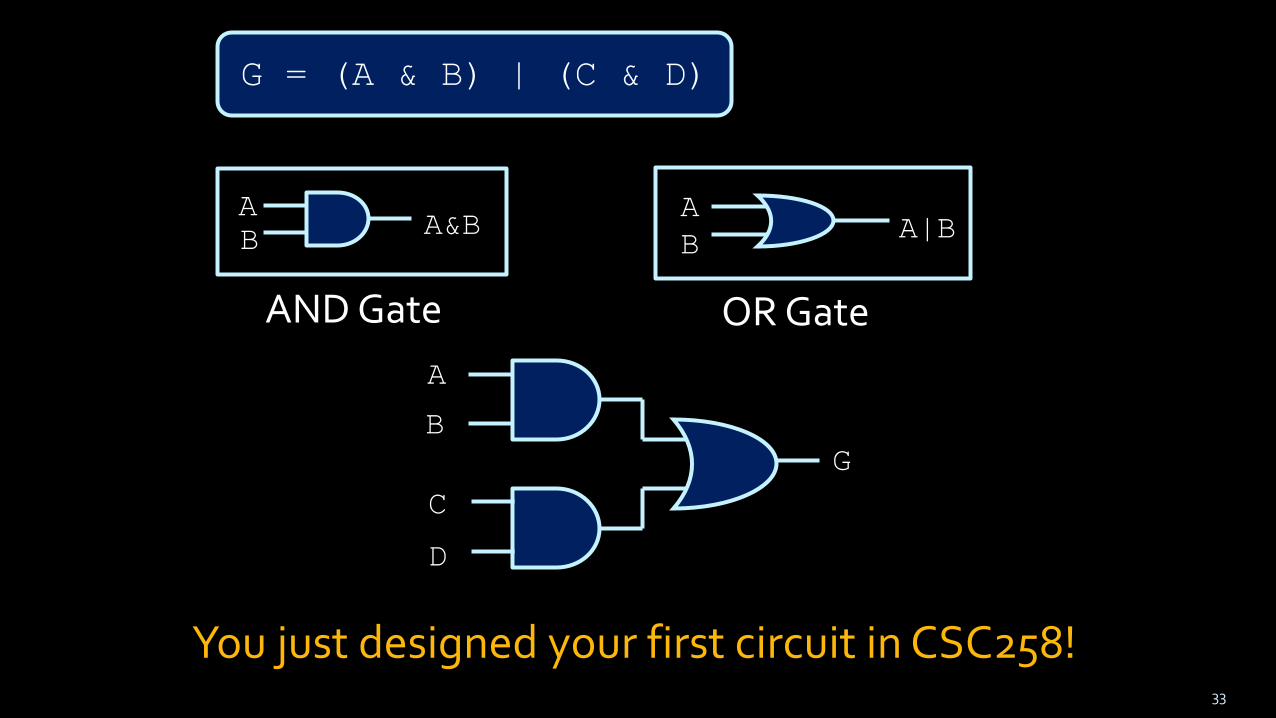
G = (A & B) | (C & D)
AB A&B
AND Gate
AB A|B
OR GateAB
CD
G
You just designed your first circuit in CSC258!33

Gates = Boolean logic
§ If we know the logical expression, we already know how to put logic gates together to form a circuit.
§ Just need to know which logic operations are represented by which gate!
Let’s meet all the gates.
34

A B Y
0 0 00 1 01 0 01 1 1
AB
Y
AND Gates
Truth table
35

A B Y
0 0 00 1 11 0 11 1 1
OR Gates
AB
Y
36

A Y
0 11 0
NOT Gates
A Y
37

A B Y
0 0 00 1 11 0 11 1 0
XOR Gates
AB
Y
38

Bill Gates
39

A B Y
0 0 10 1 11 0 11 1 0
AB
Y
NAND Gates
40

A B Y
0 0 10 1 01 0 01 1 0
AB
Y
NOR Gates
41

A Y
0 01 1
A Y
Buffer
This is not as silly as you might think now, as we’ll see later…
42
AB
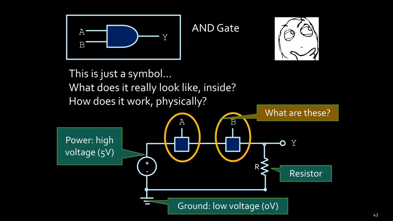
YAND Gate
This is just a symbol...What does it really look like, inside?How does it work, physically?
Y
+-
BA
R
Ground: low voltage (0V)
Power: high voltage (5V)
Resistor
What are these?
43

Y
+- R
BASwitches
When and only when both A are B are switched ON, Y has high voltage.
44

Y
+- R
BA Gates
• Gate is like a switch, but controlled by the voltage of the input signal, instead of by a finger.
• Gate A is switched ON when signal A is of high voltage.• When and only when both A and B have high voltage,
Y has high voltage.• High voltage is 1 (True), low voltage is 0 (False).• Y is True iff both A and B are True (Y = A & B).
45

A Gate is switched ON when signal A is of
high voltage …
Why?
How? What does the inside of a gate look like?
Answer: There are transistors.46

Transistors
47

One of the greatest inventions of the 20th century
§ Invented by William Shockley, John Bardeen and Walter Brattain in 1947, replacing previous vacuum-tube technology.ú Nobel Prize for Physics in
1956.
Building block for the hardware of all your computers and electronic devices.
48

What do transistors do?§ Transistors connect Point A to Point B, based on
the value at Point C.ú If the value at Point C is high, A and B are connected.
ú And if the value at Point C is low, A and B are not.
ú Need to know a little about electricity now….
A B
C = 1
A B
C = 0
A B
A B
49

50

Outline of the story
• Electricity, basic concepts
• Insulators, conductors, in between …, Semiconductors
• Impure semiconductors, p-type / n-type
• Put p-type and n-type together -- pn-junction
• Apply voltage to a pn-junction – principle of transistors
• A real-world manufacturing of transistor -- MOSFET
51

Electricity Basics
52

Everything is made out of atoms …
• Protons are big (hardly move) and positively charged.• Electrons are small
(easily move) and negatively changed.• Neutrons are big and
of course, neutral.• Overall, an atom is
neutral.53
What is Electricity?
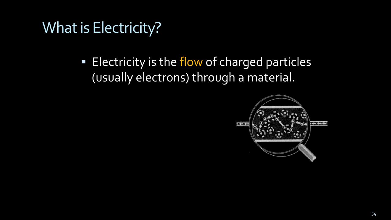
§ Electricity is the flow of charged particles (usually electrons) through a material.
54

How do electrons flow?
They flow …
55

How do electrons flow?
§ Electrons want to flow from regions of high electricalpotential (many electrons) to regions of low electrical potential (fewer electrons).ú Like water flows from high to low.
§ This potential is referred to as voltage (V).§ The rate of this flow is called the current (I).§ Resistance (I = V / R) is like how narrow the water pipe is.
56

Note
The direction of the current is opposite to the direction of the electron movement, because electrons are negatively charged.
57

More on Resistance§ Electrical resistance indicates how well a
material allows electricity to flow through it:ú High resistance (aka insulators) don’t conduct
electricity at all.ú Low resistance (aka conductors) conduct
electricity well, and are generally used for wires.
§ Semiconductors are somewhere in between conductors and insulators, which makes it interesting…
58

Outline of the story
• Electricity, basic concepts• Insulators, conductors, in between …,
Semiconductors• Impure semiconductors, p-type / n-type• Put p-type and n-type together -- pn-
junction• Apply voltage to a pn-junction – principle
of transistors• A real-world manufacturing of transistor --
MOSFET59

Semiconductors
60
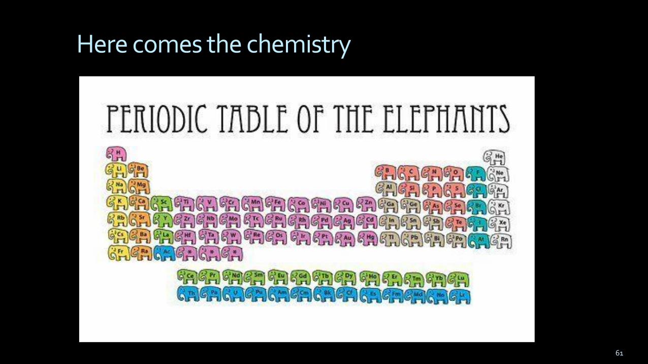
Here comes the chemistry
61
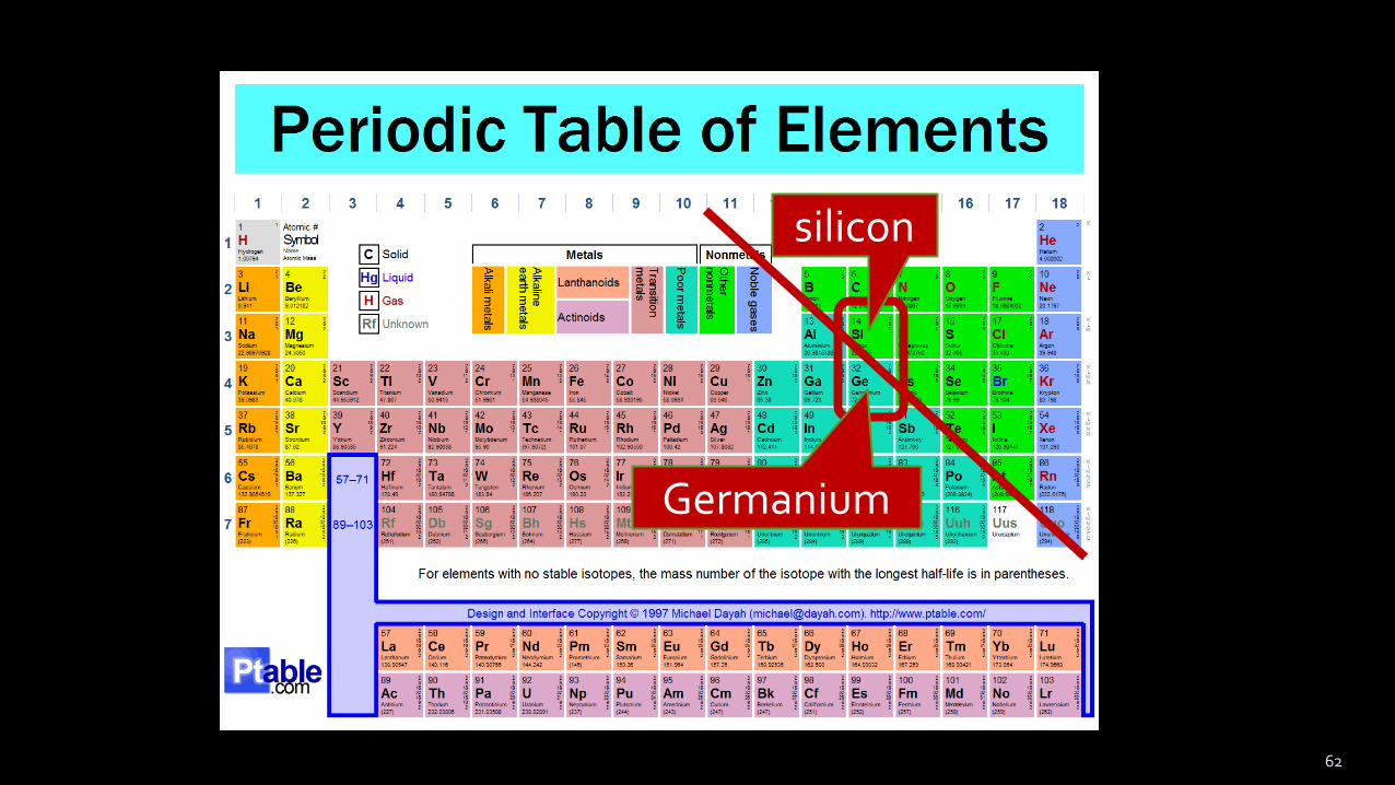
silicon
Germanium
62

Conductivity of Semiconductors
§ Semiconductor materials (e.g., silicon and germanium) straddle the boundary between conductors and insulators, behaving like one or the other, depending on factors like temperature and impurities in the material.
63

Impurity
64

Pure semiconductor is pretty stable
§ Each atom has 4 valence electrons, forming bondswith other atoms, and the structure is pretty stable.
§ At room temperature, very close to insulator.
65

Encourage semiconductor’s conductivity
N-type:Add some atoms with 5valence electrons, such as Phosphorus.
An extra electron!P-type:Add some atoms with 3valence electrons, such as Boron. A missing electron, a.k.a., a
“hole”, like a positive electron!66

Encourage semiconductor’s conductivity
The extra electrons and the holes are charge carriers, which can move freely through the materials.
Thus the conductivity is encouraged.
This process of adding stuff is called doping, (n or p type).
67

Free electrons move like
Free holes move like
68

Outline of the story
• Electricity, basic concepts• Insulators, conductors, in between …,
Semiconductors• Impure semiconductors, p-type / n-type• Put p-type and n-type together -- pn-
junction• Apply voltage to a pn-junction – principle
of transistors• A real-world manufacturing of transistor --
MOSFET69

PN-junctions
70

Bringing p and n together
§ What happens if you brought some p-type material into contact with some n-type material?
§ The electrons at the surface of the n-type material are drawn to the holes in the p-type.
Si Si
Si P
Si Si
Si Si
Si Si
Si Si
Si Si
B Si
Si
Si Si
Si
Si Si
Si
Si Si
Si Si
Si
Si Si
Si Si
Si
Si Si
Si
Si
Si Si
Si
P P P
P
B
B
B
B
-
----
--
--
-p-type
n-type
71

p-n Junctions§ When left alone, the
electrons from the nsection of the junctionwill fill the holes of the p section, cancelling each other and create a section with no free carriers called the depletion layer.
§ Once this depletion layer is wide enough, the doping atoms that remain will create an electric field in that region.
72

Si Si
Si P
Si Si
Si Si
Si Si
Si Si
Si Si
B Si
Si
Si Si
Si
Si Si
Si
Si Si
Si Si
Si
Si Si
Si Si
Si
Si Si
Si
Si
Si Si
Si
P P P
P
B
B
B
B
-
----
--
--
-
p-type
n-typeBecause lost electron
Because gained electron
Electrons’ initial movement (attracted by holes)
73

p-type
n-typeElectrons’ initial movement
(attracted by holes)
Electric field
Electron’s movement drawn by the electric field
“Diffusion”
“Drift”
Diffusion increases the width of depletion layer, and drift draws it back. An equilibrium is reached, when the depletion layer is of a certain width.
74

Analogy: Spring with weight
“Diffusion” “Drift”
Attracted by gravity (hole)
Drawn by spring force field
An equilibrium is reached when the spring is stretched by a certain length.
75
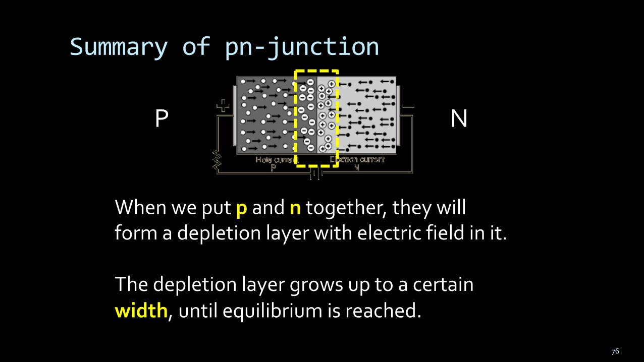
Summary of pn-junction
When we put p and n together, they will form a depletion layer with electric field in it.
The depletion layer grows up to a certain width, until equilibrium is reached.
NP
76

Outline of the story
• Electricity, basic concepts• Insulators, conductors, in between …,
Semiconductors• Impure semiconductors, p-type / n-type• Put p-type and n-type together -- pn-
junction• Apply voltage to a pn-junction – principle
of transistors• A real-world manufacturing of transistor --
MOSFET77

Apply voltage to a PN-junction
It could be applied in two possible directions
• Positive voltage to the P side
• Positive voltage to the N side
78

Forward Bias (Positive voltage to P)
P NNegative charges sucked
out of depletion layerPositive charges sucked
out of depletion layer
Depletion layer becomes narrower.79

Reverse Bias (Positive voltage to N)
P NNegative charges injected
into depletion layerPositive charges injected
into depletion layer
Depletion layer becomes wider.80

Apply forward bias• Depletion layer narrower• Easier to travel through• Better conductivity• Like switch connected
Apply reverse bias• Depletion layer wider• Harder to travel through• Worse conductivity• Like switch disconnected
That’s how transistors work!81

Outline of the story
• Electricity, basic concepts• Insulators, conductors, in between …,
Semiconductors• Impure semiconductors, p-type / n-type• Put p-type and n-type together -- pn-
junction• Apply voltage to a pn-junction – principle
of transistors• A real-world manufacturing of transistor --
MOSFET82
Creating transistors§ Transistors use the characteristics of p-n
junctions to create more interesting behaviour.
§ Three main types:ú Bipolar Junction Transistors (BJTs)ú Metal Oxide Semiconductor Field Effect Transistor
(MOSFET)ú Junction Field Effect Transistor (JFET)
§ The last two are part of the same family, but we’ll only look at the MOSFET for now.
83

Metal Oxide Semiconductor Field Effect Transistor
84

Source Drain
Gate
85

Metal Oxide
N-type P-type
GateSource Drain
InsulatorConductor, can apply electric charge to it
Semiconductors, doped
86

Put a MOSFET into a circuitGate
Source Drain
+ -- +or
Power: high voltage can be applied to
source or drain
87

Put it into a circuitGate
Source Drain
+ -- +
Metal Oxide N-type P-type
Two PN-junctions back-to-back, i.e, N-P-N. So, either source or drain has high voltage, one of the PN-junction must be reverse biased (circuit disconnected).
88

But things change if we apply high voltage to Gate
Gate
Metal Oxide N-type P-type
Attract negative charges from p-substrate
Create n-type channel between source and drain, CIRCUIT CONNECTED
The wider the channel, the higher the current89

Two types of MOSFET
• nMOS (what we just describe)• N-P-N• Gate high, connected• Gate low, disconnected
• pMOS (opposite to nMOS)• P-N-P• Gate low, connected• Gate high, disconnected
90

Outline of the story• Electricity, basic concepts• Insulators, conductors, in between …,
Semiconductors• Impure semiconductors, p-type / n-type• Put p-type and n-type together -- pn-
junction• Apply voltage to a pn-junction – principle
of transistors• A real-world manufacturing of transistor –
MOSFET• Use transistors build Logic Gates
91

Transistors to Logic Gates
92

Create gates using a combination of transistors
A Y
A Y
NOT Gate
Physical data:ú “High” input = 5V
ú “Low” input = 0V
ú Switching time: ~20 picoseconds
ú Switching interval ~10 ns
93

Transistors into gates
Y
A
B
A
B
A
B
A
B
Vcc Vcc
A
B
Y
Vcc
A B
A B
A
Y
Vcc Vcc
B
AND ORXOR
94

NAND is the most awesome logic gate• It’s cheaper to build• All other logic functions (AND,
OR, …) can be implemented using only NAND, i.e., it is functionally complete.
Challenge for home: implement AND, OR, NOT, XOR using only NAND.
95

Next week:• Circuit creation
96