Embed Size (px)
Citation preview
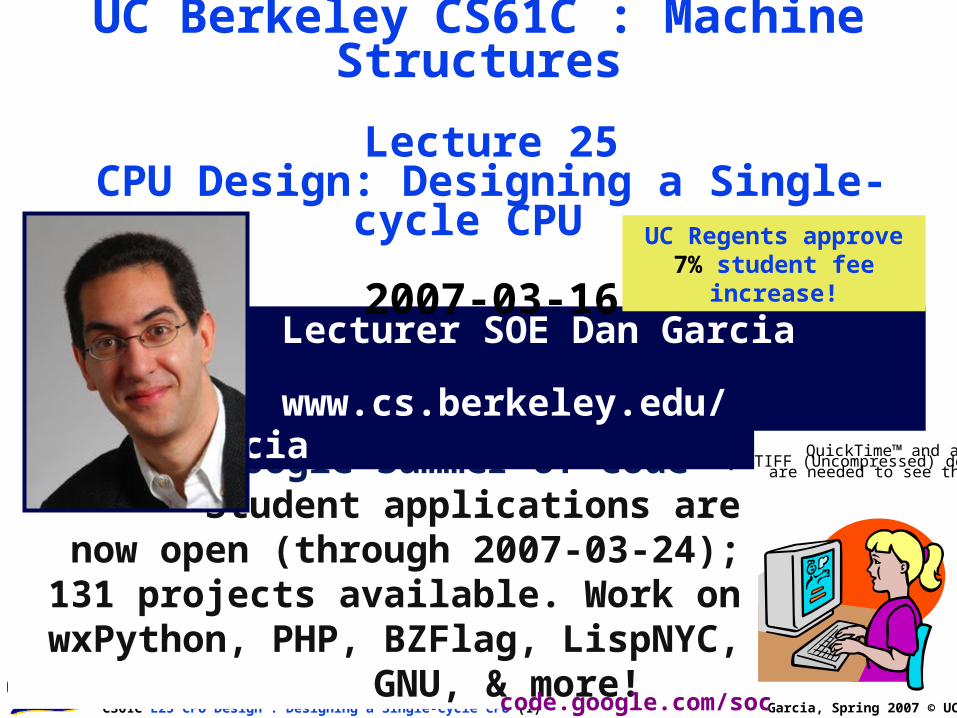
CS61C L25 CPU Design : Designing a Single-Cycle CPU (1) Garcia, Spring 2007 © UCB
Google Summer of Code Student applications are
now open (through 2007-03-24); 131 projects available. Work on wxPython,
PHP, BZFlag, LispNYC, GNU, & more!
Lecturer SOE Dan Garcia
www.cs.berkeley.edu/~ddgarcia
inst.eecs.berkeley.edu/~cs61c UC Berkeley CS61C : Machine Structures
Lecture 25 CPU Design: Designing a Single-cycle CPU
2007-03-16
code.google.com/soc
QuickTime™ and aTIFF (Uncompressed) decompressor
are needed to see this picture.
UC Regents approve 7% student fee increase!

CS61C L25 CPU Design : Designing a Single-Cycle CPU (2) Garcia, Spring 2007 © UCB
Review
• N-bit adder-subtractor done using N 1-bit adders with XOR gates on input
• XOR serves as conditional inverter
• CPU design involves Datapath,Control• Datapath in MIPS involves 5 CPU stages
1) Instruction Fetch
2) Instruction Decode & Register Read
3) ALU (Execute)
4) Memory
5) Register Write

CS61C L25 CPU Design : Designing a Single-Cycle CPU (3) Garcia, Spring 2007 © UCB
Datapath Summary• The datapath based on data transfers required to perform instructions
• A controller causes the right transfers to happen
PC
inst
ruct
ion
me
mor
y
+4
rtrs
rd
regi
ste
rs
ALU
Da
tam
em
ory
imm
Controller
opcode, funct

CS61C L25 CPU Design : Designing a Single-Cycle CPU (4) Garcia, Spring 2007 © UCB
CPU clocking (1/2)
• Single Cycle CPU: All stages of an instruction are completed within one long clock cycle.
• The clock cycle is made sufficient long to allow each instruction to complete all stages without interruption and within one cycle.
For each instruction, how do we control the flow of information though the datapath?
1. InstructionFetch
2. Decode/ Register
Read
3. Execute 4. Memory5. Reg. Write

CS61C L25 CPU Design : Designing a Single-Cycle CPU (5) Garcia, Spring 2007 © UCB
CPU clocking (2/2)
• Multiple-cycle CPU: Only one stage of instruction per clock cycle.
• The clock is made as long as the slowest stage.
Several significant advantages over single cycle execution: Unused stages in a particular instruction can be skipped OR instructions can be pipelined (overlapped).
For each instruction, how do we control the flow of information though the datapath?
1. InstructionFetch
2. Decode/ Register
Read
3. Execute 4. Memory5. Reg. Write
CS61C L25 CPU Design : Designing a Single-Cycle CPU (6) Garcia, Spring 2007 © UCB
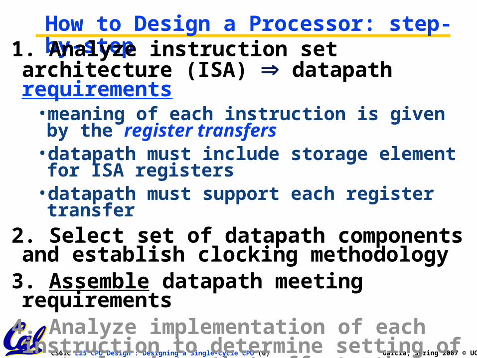
How to Design a Processor: step-by-step1. Analyze instruction set architecture (ISA)
datapath requirements• meaning of each instruction is given by the register transfers
• datapath must include storage element for ISA registers
• datapath must support each register transfer
2. Select set of datapath components and establish clocking methodology
3. Assemble datapath meeting requirements4. Analyze implementation of each instruction to determine setting of control points that effects the register transfer.
5. Assemble the control logic
CS61C L25 CPU Design : Designing a Single-Cycle CPU (7) Garcia, Spring 2007 © UCB
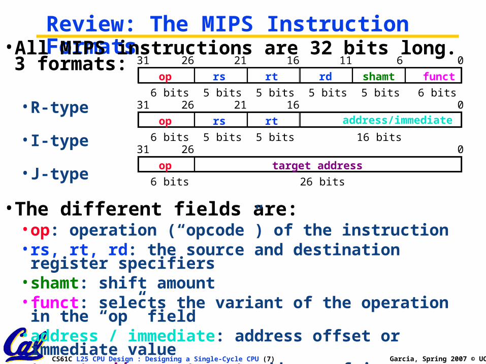
Review: The MIPS Instruction Formats• All MIPS instructions are 32 bits long. 3 formats:
• R-type
• I-type
• J-type
• The different fields are:• op: operation (“opcode”) of the instruction• rs, rt, rd: the source and destination register specifiers• shamt: shift amount• funct: selects the variant of the operation in the “op”
field• address / immediate: address offset or immediate value• target address: target address of jump instruction
op target address
02631
6 bits 26 bits
op rs rt rd shamt funct
061116212631
6 bits 6 bits5 bits5 bits5 bits5 bits
op rs rt address/immediate
016212631
6 bits 16 bits5 bits5 bits
CS61C L25 CPU Design : Designing a Single-Cycle CPU (8) Garcia, Spring 2007 © UCB
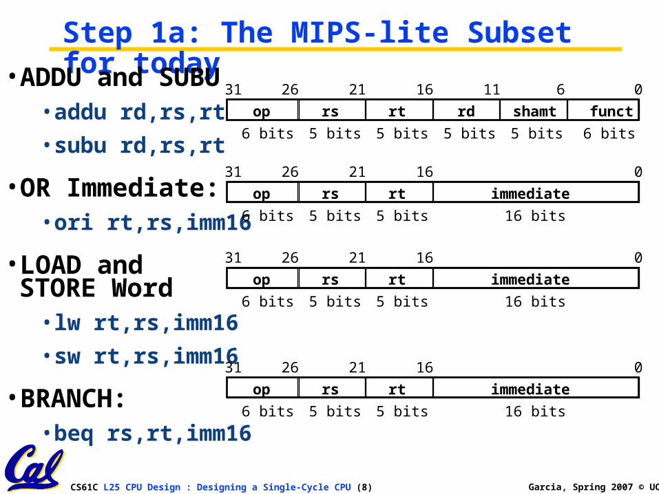
Step 1a: The MIPS-lite Subset for today
• ADDU and SUBU•addu rd,rs,rt•subu rd,rs,rt
• OR Immediate:•ori rt,rs,imm16
• LOAD and STORE Word•lw rt,rs,imm16•sw rt,rs,imm16
• BRANCH:•beq rs,rt,imm16
op rs rt rd shamt funct
061116212631
6 bits 6 bits5 bits5 bits5 bits5 bits
op rs rt immediate
016212631
6 bits 16 bits5 bits5 bits
op rs rt immediate
016212631
6 bits 16 bits5 bits5 bits
op rs rt immediate
016212631
6 bits 16 bits5 bits5 bits

CS61C L25 CPU Design : Designing a Single-Cycle CPU (9) Garcia, Spring 2007 © UCB
Register Transfer Language• RTL gives the meaning of the instructions
• All start by fetching the instruction
{op , rs , rt , rd , shamt , funct} MEM[ PC ]
{op , rs , rt , Imm16} MEM[ PC ]
inst Register Transfers
ADDU R[rd] R[rs] + R[rt]; PC PC + 4
SUBU R[rd] R[rs] – R[rt]; PC PC + 4
ORI R[rt] R[rs] | zero_ext(Imm16); PC PC + 4
LOAD R[rt] MEM[ R[rs] + sign_ext(Imm16)]; PC PC + 4
STORE MEM[ R[rs] + sign_ext(Imm16) ] R[rt]; PC PC + 4
BEQ if ( R[rs] == R[rt] ) then PC PC + 4 + (sign_ext(Imm16) || 00) else PC PC + 4
CS61C L25 CPU Design : Designing a Single-Cycle CPU (10) Garcia, Spring 2007 © UCB
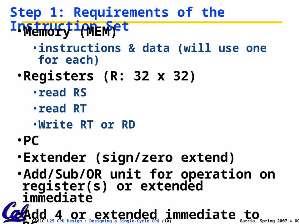
Step 1: Requirements of the Instruction Set• Memory (MEM)
• instructions & data (will use one for each)• Registers (R: 32 x 32)
• read RS• read RT• Write RT or RD
• PC• Extender (sign/zero extend)• Add/Sub/OR unit for operation on register(s) or extended immediate
• Add 4 or extended immediate to PC• Compare registers?
CS61C L25 CPU Design : Designing a Single-Cycle CPU (11) Garcia, Spring 2007 © UCB
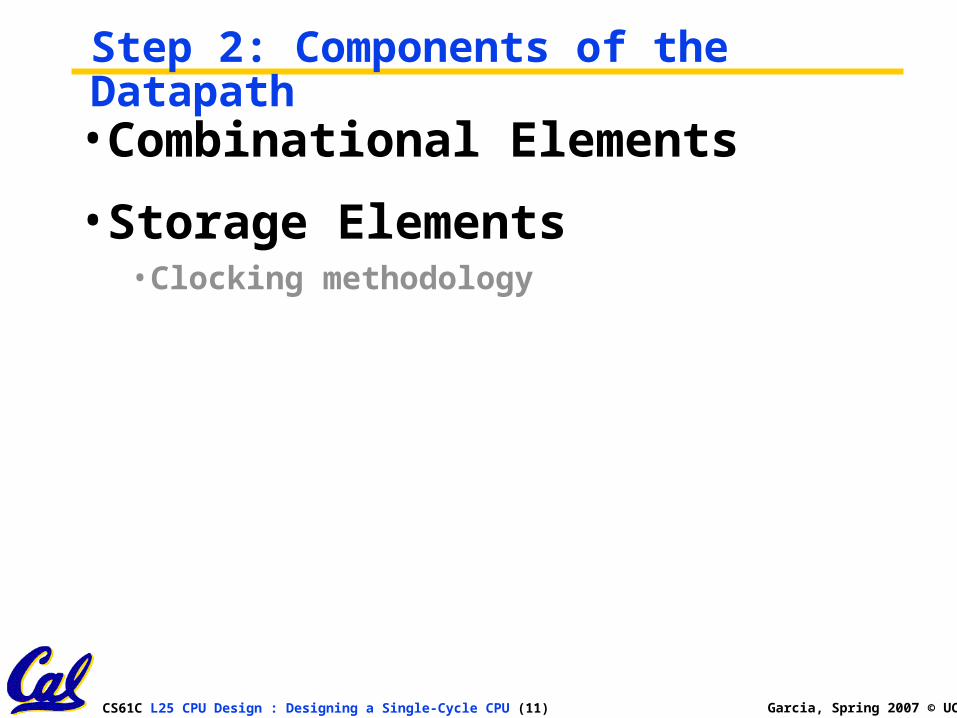
Step 2: Components of the Datapath•Combinational Elements
•Storage Elements• Clocking methodology

CS61C L25 CPU Design : Designing a Single-Cycle CPU (12) Garcia, Spring 2007 © UCB
Combinational Logic Elements (Building Blocks)
•Adder
•MUX
•ALU
32
32
A
B32
Sum
CarryOut
32
32
A
B32
Result
OP
32A
B32
Y32
Select
Ad
der
MU
XA
LU
CarryIn

CS61C L25 CPU Design : Designing a Single-Cycle CPU (13) Garcia, Spring 2007 © UCB
ALU Needs for MIPS-lite + Rest of MIPS• Addition, subtraction, logical OR, ==:
ADDU R[rd] = R[rs] + R[rt]; ...
SUBU R[rd] = R[rs] – R[rt]; ...
ORI R[rt] = R[rs] | zero_ext(Imm16)...
BEQ if ( R[rs] == R[rt] )...
• Test to see if output == 0 for any ALU operation gives == test. How?
• P&H also adds AND, Set Less Than (1 if A < B, 0 otherwise)
• ALU follows chap 5

CS61C L25 CPU Design : Designing a Single-Cycle CPU (14) Garcia, Spring 2007 © UCB
Administrivia
• Read the book! Important to understand lecture and for project.
• P&H 5.1-5.4

CS61C L25 CPU Design : Designing a Single-Cycle CPU (15) Garcia, Spring 2007 © UCB
What Hardware Is Needed? (1/2)• PC: a register which keeps track of memory addr of the next instruction
• General Purpose Registers• used in Stages 2 (Read) and 5 (Write)
• MIPS has 32 of these
• Memory• used in Stages 1 (Fetch) and 4 (R/W)
• cache system makes these two stages as fast as the others, on average
CS61C L25 CPU Design : Designing a Single-Cycle CPU (16) Garcia, Spring 2007 © UCB
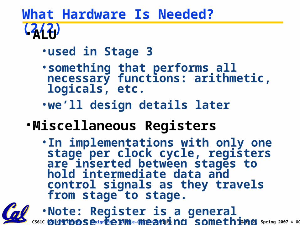
What Hardware Is Needed? (2/2)• ALU
• used in Stage 3• something that performs all necessary functions: arithmetic, logicals, etc.
• we’ll design details later
• Miscellaneous Registers• In implementations with only one stage per clock cycle, registers are inserted between stages to hold intermediate data and control signals as they travels from stage to stage.
• Note: Register is a general purpose term meaning something that stores bits. Not all registers are in the “register file”.

CS61C L25 CPU Design : Designing a Single-Cycle CPU (17) Garcia, Spring 2007 © UCB
Storage Element: Idealized Memory
• Memory (idealized)• One input bus: Data In• One output bus: Data Out
• Memory word is selected by:• Address selects the word to put on Data Out• Write Enable = 1: address selects the memory
word to be written via the Data In bus• Clock input (CLK)
• The CLK input is a factor ONLY during write operation
• During read operation, behaves as a combinational logic block:
Address valid Data Out valid after “access time.”
Clk
Data In
Write Enable
32 32DataOut
Address

CS61C L25 CPU Design : Designing a Single-Cycle CPU (18) Garcia, Spring 2007 © UCB
Storage Element: Register (Building Block)
• Similar to D Flip Flop except N-bit input and output Write Enable input
• Write Enable: negated (or deasserted) (0):
Data Out will not change asserted (1):
Data Out will become Data In on positive edge of clock
clk
Data In
Write Enable
N N
Data Out

CS61C L25 CPU Design : Designing a Single-Cycle CPU (19) Garcia, Spring 2007 © UCB
Storage Element: Register File• Register File consists of 32 registers:
• Two 32-bit output busses: busA and busB• One 32-bit input bus: busW
• Register is selected by:• RA (number) selects the register to put on busA (data)• RB (number) selects the register to put on busB (data)• RW (number) selects the register to be written
via busW (data) when Write Enable is 1• Clock input (clk)
• The clk input is a factor ONLY during write operation• During read operation, behaves as a combinational
logic block: RA or RB valid busA or busB valid after “access time.”
Clk
busW
Write Enable
3232
busA
32busB
5 5 5RWRA RB
32 32-bitRegisters

CS61C L25 CPU Design : Designing a Single-Cycle CPU (20) Garcia, Spring 2007 © UCB
Step 3: Assemble DataPath meeting requirements
• Register Transfer Requirements Datapath Assembly
• Instruction Fetch
• Read Operands and Execute Operation

CS61C L25 CPU Design : Designing a Single-Cycle CPU (21) Garcia, Spring 2007 © UCB
3a: Overview of the Instruction Fetch Unit
• The common RTL operations• Fetch the Instruction: mem[PC]• Update the program counter:
Sequential Code: PC PC + 4 Branch and Jump: PC “something else”
32
Instruction WordAddress
InstructionMemory
PCclk
Next AddressLogic
CS61C L25 CPU Design : Designing a Single-Cycle CPU (22) Garcia, Spring 2007 © UCB
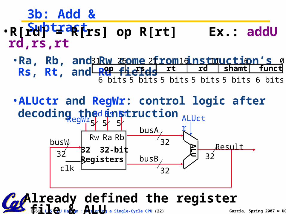
3b: Add & Subtract• R[rd] = R[rs] op R[rt] Ex.: addU rd,rs,rt
• Ra, Rb, and Rw come from instruction’s Rs, Rt, and Rd fields
• ALUctr and RegWr: control logic after decoding the instruction
32Result
ALUctr
clk
busW
RegWr
32
32
busA
32
busB
5 5 5
Rw Ra Rb
32 32-bitRegisters
Rs RtRd
AL
U
op rs rt rd shamt funct061116212631
6 bits 6 bits5 bits5 bits5 bits5 bits
Already defined the register file & ALU

CS61C L25 CPU Design : Designing a Single-Cycle CPU (23) Garcia, Spring 2007 © UCB
Peer Instruction
A. Our ALU is a synchronous device
B. We should use the main ALU to compute PC=PC+4
C. The ALU is inactive for memory reads or writes.
ABC1: FFF2: FFT3: FTF4: FTT5: TFF6: TFT7: TTF8: TTT

CS61C L25 CPU Design : Designing a Single-Cycle CPU (24) Garcia, Spring 2007 © UCB
Peer Instruction
A. If the destination reg is the same as the source reg, we could compute the incorrect value!
B. We’re going to be able to read 2 registers and write a 3rd in 1 cycle
C. Datapath is hard, Control is easy
ABC0: FFF1: FFT2: FTF3: FTT4: TFF5: TFT6: TTF7: TTT
CS61C L25 CPU Design : Designing a Single-Cycle CPU (25) Garcia, Spring 2007 © UCB
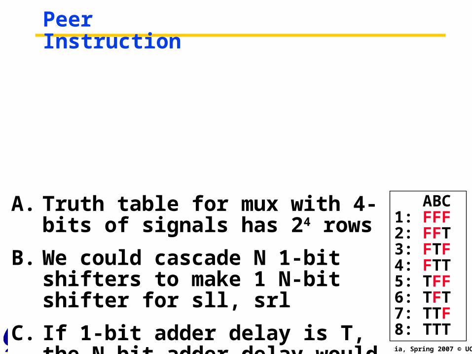
Peer Instruction
A. Truth table for mux with 4-bits of signals has 24 rows
B. We could cascade N 1-bit shifters to make 1 N-bit shifter for sll, srl
C. If 1-bit adder delay is T, the N-bit adder delay would also be T
ABC1: FFF2: FFT 3: FTF4: FTT5: TFF6: TFT7: TTF8: TTT
CS61C L25 CPU Design : Designing a Single-Cycle CPU (26) Garcia, Spring 2007 © UCB
Peer Instruction Answer
A. Truth table for mux with 4-bits of signals is 24 rows long
B. We could cascade N 1-bit shifters to make 1 N-bit shifter for sll, srl
C. If 1-bit adder delay is T, the N-bit adder delay would also be T
ABC1: FFF2: FFT 3: FTF4: FTT5: TFF6: TFT7: TTF8: TTT
A. Truth table for mux with 4-bits of signals controls 16 inputs, for a total of 20 inputs, so truth table is 220 rows…FALSE
B. We could cascade N 1-bit shifters to make 1 N-bit shifter for sll, srl … TRUE
C. What about the cascading carry? FALSE

CS61C L25 CPU Design : Designing a Single-Cycle CPU (27) Garcia, Spring 2007 © UCB
How to Design a Processor: step-by-step• 1. Analyze instruction set architecture (ISA)
datapath requirements• meaning of each instruction is given by the register transfers
• datapath must include storage element for ISA registers
• datapath must support each register transfer• 2. Select set of datapath components and establish clocking methodology
• 3. Assemble datapath meeting requirements• 4. Analyze implementation of each instruction to determine setting of control points that effects the register transfer.
• 5. Assemble the control logic (hard part!)


![L25-L100 User Manual[1]](https://img.pdfslide.us/doc/110x75/577d27ab1a28ab4e1ea4808e/l25-l100-user-manual1.jpg)