Embed Size (px)
Citation preview

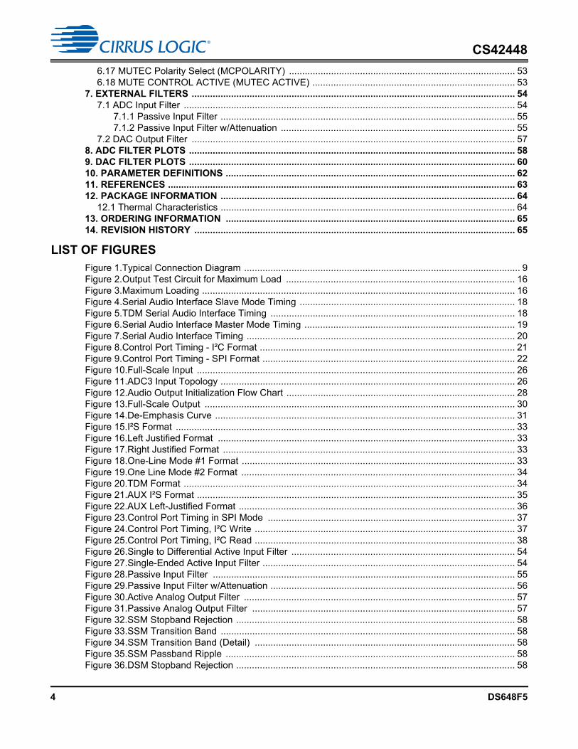
CS42448
108 dB, 192 kHz 6-In, 8-Out CODEC
FEATURESSix 24-bit A/D, Eight 24-bit D/A Converters
ADC Dynamic Range– 105 dB Differential– 102 dB Single-Ended
DAC Dynamic Range– 108 dB Differential– 105 dB Single-Ended
ADC/DAC THD+N– -98 dB Differential– -95 dB Single-Ended
Compatible with Industry-Standard Time Division Multiplexed (TDM) Serial Interface
System Sampling Rates up to 192 kHz
Programmable ADC High-Pass Filter for DC Offset Calibration
Logarithmic Digital Volume Control
I²C™ & SPI™ Host Control Port
Supports Logic Levels Between 5 V and 1.8 V
Popguard® Technology
GENERAL DESCRIPTION
The CS42448 CODEC provides six multi-bit ana-log-to-digital and eight multi-bit digital-to-analogdelta-sigma converters. The CODEC is capable of op-eration with either differential or single-ended inputsand outputs, in a 64-pin LQFP package.
Six fully differential, or single-ended, inputs are avail-able on stereo ADC1, ADC2, and ADC3. Whenoperating in Single-Ended Mode, an internal MUX be-fore ADC3 allows selection from up to four single-endedinputs. Digital volume control is provided for each ADCchannel, with selectable overflow detection.
All eight DAC channels provide digital volume controland can operate with differential or single-endedoutputs.
An auxiliary serial input is available for an additional twochannels of PCM data.
The CS42448 is available in a 64-pin LQFP package inCommercial (-10°C to +70°C) and Automotive (-40°C to+105°C) grades. The CDB42448 Customer Demonstra-tion Board is also available for device evaluation andimplementation suggestions. Please refer to “OrderingInformation” on page 65 for complete orderinginformation.
The CS42448 is ideal for audio systems requiring widedynamic range, negligible distortion and low noise, suchas A/V receivers, DVD receivers, and automotive audiosystems.
Control Port & Serial Audio Port Supply = 1.8 V to 5 V
Mute Control
ExternalMute Control
Register Configuration Internal Voltage
Reference
Reset
PC
M o
r T
DM
Ser
ial
Inte
rfac
e
Leve
l Tra
nsla
tor
Serial Audio Input
Digital Supply = 3.3 V to 5 V
Analog Supply = 3.3 V to 5 V
Input Master Clock
Serial Audio Output
MultibitOversampling
ADC1&2
High Pass Filter
Differential or Single-Ended Analog Inputs
4DigitalFilters
4
*Optional MUX allows selection from up to 4 single-ended inputs.
MultibitOversampling
ADC3
High Pass Filter
2DigitalFilters
2
4:2*
Auxilliary Serial Audio Input
VolumeControls
Differential or Single-Ended Outputs
DigitalFilters
8Multibit
DAC1-4 and Analog Filters
8
Modulators
Interrupt ADC Overflow & Clock Error
InterruptLeve
l Tra
nsla
torI2C/SPI
Software ModeControl Data
Copyright Cirrus Logic, Inc. 2017(All Rights Reserved)
http://www.cirrus.com
MAR '17DS648F5

CS42448
TABLE OF CONTENTS1. PIN DESCRIPTIONS ...................................................................................................................... 6
1.1 Digital I/O Pin Characteristics .......................................................................................................... 82. TYPICAL CONNECTION DIAGRAM ..................................................................................................... 93. CHARACTERISTICS AND SPECIFICATIONS .................................................................................... 10
RECOMMENDED OPERATING CONDITIONS ................................................................................... 10ABSOLUTE MAXIMUM RATINGS ....................................................................................................... 10ANALOG INPUT CHARACTERISTICS (COMMERCIAL) .................................................................... 11ANALOG INPUT CHARACTERISTICS (AUTOMOTIVE) ..................................................................... 12ADC DIGITAL FILTER CHARACTERISTICS ....................................................................................... 13ANALOG OUTPUT CHARACTERISTICS (COMMERCIAL) ................................................................ 14ANALOG OUTPUT CHARACTERISTICS (AUTOMOTIVE) ................................................................. 15COMBINED DAC INTERPOLATION & ON-CHIP ANALOG FILTER RESPONSE .............................. 17SWITCHING SPECIFICATIONS - ADC/DAC PORT ............................................................................ 18SWITCHING CHARACTERISTICS - AUX PORT ................................................................................. 20SWITCHING SPECIFICATIONS - CONTROL PORT - I²C MODE ....................................................... 21SWITCHING SPECIFICATIONS - CONTROL PORT - SPI FORMAT ................................................. 22DC ELECTRICAL CHARACTERISTICS .............................................................................................. 23DIGITAL INTERFACE SPECIFICATIONS & CHARACTERISTICS ..................................................... 24
4. APPLICATIONS ................................................................................................................................... 254.1 Overview ......................................................................................................................................... 254.2 Analog Inputs .................................................................................................................................. 25
4.2.1 Line-Level Inputs ................................................................................................................... 254.2.2 ADC3 Analog Input ................................................................................................................ 264.2.3 High-Pass Filter and DC Offset Calibration ........................................................................... 27
4.3 Analog Outputs ............................................................................................................................... 274.3.1 Initialization ............................................................................................................................ 274.3.2 Output Transient Control ....................................................................................................... 294.3.3 Popguard ............................................................................................................................... 29
4.3.3.1 Power-Up ................................................................................................................... 294.3.3.2 Power-Down .............................................................................................................. 29
4.3.4 Mute Control .......................................................................................................................... 294.3.5 Line-Level Outputs and Filtering ........................................................................................... 304.3.6 Digital Volume Control ........................................................................................................... 304.3.7 De-Emphasis Filter ................................................................................................................ 30
4.4 System Clocking ............................................................................................................................. 314.5 CODEC Digital Interface Formats .................................................................................................. 32
4.5.1 I²S .......................................................................................................................................... 334.5.2 Left-Justified .......................................................................................................................... 334.5.3 Right-Justified ........................................................................................................................ 334.5.4 OLM #1 .................................................................................................................................. 334.5.5 OLM #2 .................................................................................................................................. 344.5.6 TDM ....................................................................................................................................... 344.5.7 I/O Channel Allocation ........................................................................................................... 35
4.6 AUX Port Digital Interface Formats ................................................................................................ 354.6.1 I²S .......................................................................................................................................... 354.6.2 Left-Justified .......................................................................................................................... 36
4.7 Control Port Description and Timing ............................................................................................... 364.7.1 SPI Mode ............................................................................................................................... 364.7.2 I²C Mode ................................................................................................................................ 37
4.8 Interrupts ........................................................................................................................................ 384.9 Recommended Power-Up Sequence ............................................................................................. 394.10 Reset and Power-Up .................................................................................................................... 39
2 DS648F5

CS42448
4.11 Power Supply, Grounding, and PCB Layout ................................................................................ 395. REGISTER QUICK REFERENCE ........................................................................................................ 406. REGISTER DESCRIPTION .................................................................................................................. 42
6.1 Memory Address Pointer (MAP) ..................................................................................................... 426.1.1 Increment (INCR) .................................................................................................................. 426.1.2 Memory Address Pointer (MAP[6:0]) ..................................................................................... 42
6.2 Chip I.D. and Revision Register (Address 01h) (Read Only) ......................................................... 426.2.1 Chip I.D. (CHIP_ID[3:0]) ........................................................................................................ 426.2.2 Chip Revision (REV_ID[3:0]) ................................................................................................. 42
6.3 Power Control (Address 02h) ......................................................................................................... 436.3.1 Power Down ADC Pairs (PDN_ADCX) ................................................................................. 436.3.2 Power Down DAC Pairs (PDN_DACX) ................................................................................. 436.3.3 Power Down (PDN) ............................................................................................................... 43
6.4 Functional Mode (Address 03h) ..................................................................................................... 446.4.1 DAC Functional Mode (DAC_FM[1:0]) .................................................................................. 446.4.2 ADC Functional Mode (ADC_FM[1:0]) .................................................................................. 446.4.3 MCLK Frequency (MFREQ[2:0]) ........................................................................................... 44
6.5 Interface Formats (Address 04h) .................................................................................................... 456.5.1 Freeze Controls (FREEZE) ................................................................................................... 456.5.2 Auxiliary Digital Interface Format (AUX_DIF) ........................................................................ 456.5.3 DAC Digital Interface Format (DAC_DIF[2:0]) ....................................................................... 456.5.4 ADC Digital Interface Format (ADC_DIF[2:0]) ....................................................................... 46
6.6 ADC Control & DAC De-Emphasis (Address 05h) ......................................................................... 466.6.1 ADC1-2 High-Pass Filter Freeze (ADC1-2_HPF FREEZE) .................................................. 466.6.2 ADC3 High Pass Filter Freeze (ADC3_HPF FREEZE) ......................................................... 476.6.3 DAC De-Emphasis Control (DAC_DEM) ............................................................................... 476.6.4 ADC1 Single-Ended Mode (ADC1 SINGLE) ......................................................................... 476.6.5 ADC2 Single-Ended Mode (ADC2 SINGLE) ......................................................................... 476.6.6 ADC3 Single-Ended Mode (ADC3 SINGLE) ......................................................................... 486.6.7 Analog Input Ch. 5 Multiplexer (AIN5_MUX) ......................................................................... 486.6.8 Analog Input Ch. 6 Multiplexer (AIN6_MUX) ......................................................................... 48
6.7 Transition Control (Address 06h) .................................................................................................... 486.7.1 Single Volume Control (DAC_SNGVOL, ADC_SNGVOL) .................................................... 486.7.2 Soft Ramp and Zero Cross Control (ADC_SZC[1:0], DAC_SZC[1:0]) .................................. 496.7.3 Auto-Mute (AMUTE) .............................................................................................................. 496.7.4 Mute ADC Serial Port (MUTE ADC_SP) ............................................................................... 50
6.8 DAC Channel Mute (Address 07h) ................................................................................................. 506.8.1 Independent Channel Mute (AOUTX_MUTE) ....................................................................... 50
6.9 AOUTX Volume Control (Addresses 08h- 0Fh) .......................................................................... 506.9.1 Volume Control (AOUTX_VOL[7:0]) ...................................................................................... 50
6.10 DAC Channel Invert (Address 10h) .............................................................................................. 516.10.1 Invert Signal Polarity (INV_AOUTX) .................................................................................... 51
6.11 AINX Volume Control (Address 11h-16h) ..................................................................................... 516.11.1 AINX Volume Control (AINX_VOL[7:0]) .............................................................................. 51
6.12 ADC Channel Invert (Address 17h) .............................................................................................. 516.12.1 Invert Signal Polarity (INV_AINX) ........................................................................................ 51
6.13 Status Control (Address 18h) ....................................................................................................... 526.13.1 Interrupt Pin Control (INT[1:0]) ............................................................................................ 52
6.14 Status (Address 19h) (Read Only) ............................................................................................... 526.14.1 DAC CLOCK ERROR (DAC_CLK ERROR) ....................................................................... 526.14.2 ADC CLOCK ERROR (ADC_CLK ERROR) ....................................................................... 526.14.3 ADC Overflow (ADCX_OVFL) ............................................................................................. 52
6.15 Status Mask (Address 1Ah) .......................................................................................................... 536.16 MUTEC Pin Control (Address 1Bh) .............................................................................................. 53
DS648F5 3
CS42448
6.17 MUTEC Polarity Select (MCPOLARITY) ...................................................................................... 536.18 MUTE CONTROL ACTIVE (MUTEC ACTIVE) ............................................................................. 53
7. EXTERNAL FILTERS ........................................................................................................................... 547.1 ADC Input Filter .............................................................................................................................. 54
7.1.1 Passive Input Filter ................................................................................................................ 557.1.2 Passive Input Filter w/Attenuation ......................................................................................... 55
7.2 DAC Output Filter ........................................................................................................................... 578. ADC FILTER PLOTS ............................................................................................................................ 589. DAC FILTER PLOTS ............................................................................................................................ 6010. PARAMETER DEFINITIONS .............................................................................................................. 6211. REFERENCES .................................................................................................................................... 6312. PACKAGE INFORMATION ................................................................................................................ 64
12.1 Thermal Characteristics ................................................................................................................ 6413. ORDERING INFORMATION .............................................................................................................. 6514. REVISION HISTORY .......................................................................................................................... 65
LIST OF FIGURESFigure 1.Typical Connection Diagram ......................................................................................................... 9Figure 2.Output Test Circuit for Maximum Load ....................................................................................... 16Figure 3.Maximum Loading ....................................................................................................................... 16Figure 4.Serial Audio Interface Slave Mode Timing .................................................................................. 18Figure 5.TDM Serial Audio Interface Timing ............................................................................................. 18Figure 6.Serial Audio Interface Master Mode Timing ................................................................................ 19Figure 7.Serial Audio Interface Timing ...................................................................................................... 20Figure 8.Control Port Timing - I²C Format ................................................................................................. 21Figure 9.Control Port Timing - SPI Format ................................................................................................ 22Figure 10.Full-Scale Input ......................................................................................................................... 26Figure 11.ADC3 Input Topology ................................................................................................................ 26Figure 12.Audio Output Initialization Flow Chart ....................................................................................... 28Figure 13.Full-Scale Output ...................................................................................................................... 30Figure 14.De-Emphasis Curve .................................................................................................................. 31Figure 15.I²S Format ................................................................................................................................. 33Figure 16.Left Justified Format ................................................................................................................. 33Figure 17.Right Justified Format ............................................................................................................... 33Figure 18.One-Line Mode #1 Format ........................................................................................................ 33Figure 19.One Line Mode #2 Format ........................................................................................................ 34Figure 20.TDM Format .............................................................................................................................. 34Figure 21.AUX I²S Format ......................................................................................................................... 35Figure 22.AUX Left-Justified Format ......................................................................................................... 36Figure 23.Control Port Timing in SPI Mode .............................................................................................. 37Figure 24.Control Port Timing, I²C Write ................................................................................................... 37Figure 25.Control Port Timing, I²C Read ................................................................................................... 38Figure 26.Single to Differential Active Input Filter ..................................................................................... 54Figure 27.Single-Ended Active Input Filter ................................................................................................ 54Figure 28.Passive Input Filter ................................................................................................................... 55Figure 29.Passive Input Filter w/Attenuation ............................................................................................. 56Figure 30.Active Analog Output Filter ....................................................................................................... 57Figure 31.Passive Analog Output Filter .................................................................................................... 57Figure 32.SSM Stopband Rejection .......................................................................................................... 58Figure 33.SSM Transition Band ................................................................................................................ 58Figure 34.SSM Transition Band (Detail) ................................................................................................... 58Figure 35.SSM Passband Ripple .............................................................................................................. 58Figure 36.DSM Stopband Rejection .......................................................................................................... 58
4 DS648F5

CS42448
Figure 37.DSM Transition Band ................................................................................................................ 58Figure 38.DSM Transition Band (Detail) ................................................................................................... 59Figure 39.DSM Passband Ripple .............................................................................................................. 59Figure 40.QSM Stopband Rejection ......................................................................................................... 59Figure 41.QSM Transition Band ................................................................................................................ 59Figure 42.QSM Transition Band (Detail) ................................................................................................... 59Figure 43.QSM Passband Ripple .............................................................................................................. 59Figure 44.SSM Stopband Rejection .......................................................................................................... 60Figure 45.SSM Transition Band ................................................................................................................ 60Figure 46.SSM Transition Band (detail) .................................................................................................... 60Figure 47.SSM Passband Ripple .............................................................................................................. 60Figure 48.DSM Stopband Rejection .......................................................................................................... 60Figure 49.DSM Transition Band ................................................................................................................ 60Figure 50.DSM Transition Band (detail) .................................................................................................... 61Figure 51.DSM Passband Ripple .............................................................................................................. 61Figure 52.QSM Stopband Rejection ......................................................................................................... 61Figure 53.QSM Transition Band ................................................................................................................ 61Figure 54.QSM Transition Band (detail) .................................................................................................... 61Figure 55.QSM Passband Ripple .............................................................................................................. 61
LIST OF TABLESTable 1. I/O Power Rails ............................................................................................................................. 8Table 2. Single-Speed Mode Common Frequencies ................................................................................ 31Table 3. Double-Speed Mode Common Frequencies ............................................................................... 31Table 4. Quad-Speed Mode Common Frequencies ................................................................................. 31Table 5. I²S, LJ, RJ Clock Ratios .............................................................................................................. 32Table 6. OLM #1 Clock Ratios .................................................................................................................. 32Table 7. OLM #2 Clock Ratios .................................................................................................................. 32Table 8. TDM Clock Ratios ....................................................................................................................... 32Table 9. Serial Audio Interface Channel Allocations ................................................................................. 35Table 10. MCLK Frequency Settings for I²S, Left and Right Justified Interface Formats .......................... 44Table 12. DAC Digital Interface Formats .................................................................................................. 45Table 11. MCLK Frequency Settings for TDM & OLM Interface Formats ................................................. 45Table 13. ADC Digital Interface Formats .................................................................................................. 46Table 14. Example AOUT Volume Settings .............................................................................................. 50Table 15. Example AIN Volume Settings .................................................................................................. 51
DS648F5 5

CS42448
1. PIN DESCRIPTIONS
Pin Name # Pin Description
AD0/CS 1Address Bit [0]/ Chip Select (Input) - Chip address bit in I²C Mode. Control signal used to select the chip in SPI Mode.
AD1/CDIN 2 Address Bit [1]/ SPI Data Input (Input) - Chip address bit in I²C Mode. Input for SPI data.
RST 3Reset (Input) - The device enters a low power mode and all internal registers are reset to their default settings when low.
VLC 4Control Port Power (Input) - Determines the required signal level for the control port. See “Digital I/O Pin Characteristics” on page 8.
ADC_LRCK 5ADC Left/Right Clock (Input/Output) - Determines which channel, Left or Right, is currently active on the ADC serial audio data line. Signals the start of a new TDM frame in the TDM digital interface format.
VD 6, 24 Digital Power (Input) - Positive terminal of the power supply for the digital section.
DGND7, 23,
62Digital Ground (Input) - Ground terminal of the power supply for the digital section.
VLS 8Serial Port Interface Power (Input) - Determines the required signal level for the serial inter-faces. See “Digital I/O Pin Characteristics” on page 8.
ADC_SCLK 9ADC Serial Clock (Input/Output) - Serial clock for the ADC serial audio interface. Input frequency must be 256xFs in the TDM digital interface format.
MCLK 10 Master Clock (Input) - Clock source for the delta-sigma modulators and digital filters.
ADC_SDOUT1ADC_SDOUT2ADC_SDOUT3
131211
Serial Audio Data Output (Output) - Outputs for two’s complement serial audio data.
1
2
3
4
5
6
7
8
9
10
11
12
13
14
15
16
17 18 19 20 21 22 23 24 25 26 27 28 29 30 31 32
48
47
46
45
44
43
42
41
40
39
38
37
36
35
34
33
DA
C_S
DIN
1
ADC_SCLK
ADC_LRCK
VLC
SC
L/C
CLK
AD1/CDIN
INT
VQ
FIL
T+
_AD
C
VD
VLS
MCLK
DAC_SDIN4
DAC_SDIN3
DAC_SDIN2
DG
ND
AIN1-
AIN1+
MUTEC
AOUT7+
AOUT7-
AOUT6-
AOUT6+
AOUT5+
AOUT5-
64 63 62 61 60 59 58 57 56 55 54 53 52 51 50 49
AO
UT
1-
AO
UT
2-
AO
UT
2+
AO
UT
1+
AGND
VA
AO
UT
3-
AO
UT
4-
AO
UT
4+
AO
UT
3+
AOUT8-
AOUT8+
AIN
5-/A
IN5B
AIN
5+/A
IN5A
FIL
T+
_DA
C
RST
ADC_SDOUT3
ADC_SDOUT2
ADC_SDOUT1
SD
A/C
DO
UT
AD0/CS
VD
DGND
AIN2-
AIN2+
AIN
6+/A
IN6A
AIN
6-/A
IN6B
DA
C_L
RC
K
DA
C_S
CLK
AU
X_S
CLK
AU
X_L
RC
K
AU
X_S
DIN
DG
ND
AIN
4+
AIN
4-
AIN
3+
AIN
3-
VA
AG
ND
CS42448
6 DS648F5

CS42448
DAC_SDIN1DAC_SDIN2DAC_SDIN3DAC_SDIN4
17161514
DAC Serial Audio Data Input (Input) - Input for two’s complement serial audio data.
DAC_SCLK 18DAC Serial Clock (Input/Output) - Serial clock for the DAC serial audio interface. Input frequency must be 256xFs in the TDM digital interface format.
DAC_LRCK 19DAC Left/Right Clock (Input/Output) - Determines which channel, Left or Right, is currently active on the DAC serial audio data line. Signals the start of a new TDM frame in the TDM digital interface format.
AUX_LRCK 20Auxiliary Left/Right Clock (Output) - Determines which channel, Left or Right, is currently active on the Auxiliary serial audio data line. Derived from the ADC serial port and equals Fs.
AUX_SCLK 21 Auxiliary Serial Clock (Output) - Serial clock for the Auxiliary serial audio interface.
AUX_SDIN 22Auxiliary Serial Input (Input) - Provides an additional serial input for two’s complement serial audio data. Used only in the TDM digital interface format.
AOUT1 +,-AOUT2 +,-AOUT3 +,-AOUT4 +,-AOUT5 +,-AOUT6 +,-AOUT7 +,-AOUT8 +,-
26,2527,2830,29 31,3234,3336,3739,3840,41
Differential Analog Output (Output) - The full-scale analog output level is specified in the Analog Characteristics table. Each leg of the differential outputs may also be used single-ended.
AGND 42,56 Analog Ground (Input) - Ground reference for the analog section.
VQ 43 Quiescent Voltage (Output) - Filter connection for internal quiescent reference voltage.
VA 44,53Analog Power (Input) - Positive power supply for the analog section. See “Digital I/O Pin Charac-teristics” on page 8.
AIN1 +,-AIN2 +,-AIN3 +,-AIN4 +,-AIN5 +,-AIN6 +,-
46,4548,4750,4952,5158,5760,59
Differential Analog Input (Input) - Signals are presented differentially or single-ended to the delta-sigma modulators. The full-scale input level is specified in the Analog Characteristics speci-fication table. See below for a description of AIN5-AIN6 in Single-Ended Mode.
AIN5 A,BAIN6 A,B
58,5760,59
Single-Ended Analog Input (Input) - When stereo ADC3 is in Single-Ended Mode, an internal analog mux allows selection between 2 channels for both analog inputs AIN5 and AIN6 (see Sec-tion 4.2.2 on page 26 for details). The unused leg of each input is internally connected to common mode. The full-scale input level is specified in the Analog Characteristics table.
MUTEC 35Mute Control (Output) - Used as a control for external mute circuits to prevent the clicks and pops that can occur in any single supply system.
FILT+_DAC 54Positive Voltage Reference (Output) - Positive reference voltage for the internal sampling cir-cuits of the DAC.
FILT+_ADC 55Positive Voltage Reference (Output) - Positive reference voltage for the internal sampling cir-cuits of the ADC.
INT 61Interrupt (Output) - Signals either an ADC overflow condition has occurred in one or more of the ADC inputs, or a clocking error has occurred in the DAC/ADC as specified in the Interrupt register.
SCL/CCLK 63 Serial Control Port Clock (Input) - Serial clock for the control port interface.
SDA/CDOUT 64 Serial Control Data I/O (Input/Output) - Input/Output for I²C data. Output for SPI data.
DS648F5 7

CS42448
1.1 Digital I/O Pin Characteristics
Various pins on the CS42448 are powered from separate power supply rails. The logic level for each inputshould adhere to the corresponding power rail and should not exceed the maximum ratings.
Power Rail
Pin Name I/O Driver Receiver
VLC RST Input - 1.8 V - 5.0 V, CMOS
SCL/CCLK Input - 1.8 V - 5.0 V, CMOS, with Hysteresis
SDA/CDOUTInput/Output
1.8 V - 5.0 V, CMOS/Open Drain 1.8 V - 5.0 V, CMOS, with Hysteresis
AD0/CS Input - 1.8 V - 5.0 V, CMOS
AD1/CDIN Input - 1.8 V - 5.0 V, CMOS
INT Output 1.8 V - 5.0 V, CMOS/Open Drain -
VLS MCLK Input - 1.8 V - 5.0 V, CMOS
ADC_LRCKInput/Output
1.8 V - 5.0 V, CMOS 1.8 V - 5.0 V, CMOS
ADC_SCLKInput/Output
1.8 V - 5.0 V, CMOS 1.8 V - 5.0 V, CMOS
ADC_SDOUT1-3 Output 1.8 V - 5.0 V, CMOS -
DAC_LRCKInput/Output
1.8 V - 5.0 V, CMOS 1.8 V - 5.0 V, CMOS
DAC_SCLKInput/Output
1.8 V - 5.0 V, CMOS 1.8 V - 5.0 V, CMOS
DAC_SDIN1-4 Input - 1.8 V - 5.0 V, CMOS
AUX_LRCK Output 1.8 V - 5.0 V, CMOS -
AUX_SCLK Output 1.8 V - 5.0 V, CMOS -
AUX_SDIN Input - 1.8 V - 5.0 V, CMOS
VA MUTEC Output 3.3 V - 5.0 V, CMOS -
Table 1. I/O Power Rails
8 DS648F5
CS42448
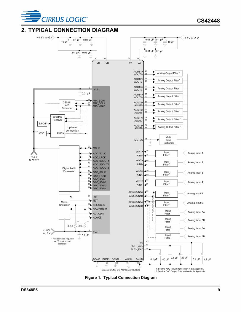
2. TYPICAL CONNECTION DIAGRAM
0.1 µF
100 µF 0.1 µF
+ +
VQ
FILT+_DAC
0.1 µF 4.7 µF
VA
0.01 µF
DGND
0.1 µF
+1.8 Vto +5 V
Digital Audio Processor
Micro-Controller
CS5341A/D
Converter
VAVD
AGNDAGND
Connect DGND and AGND near CODEC
0.01 µF
0.1 µF +10 µF
0.01 µF+3.3 V to +5 V
+10 µF
0.1 µF 0.01 µF
+1.8 Vto +5.0 V
S/PDIF
CS8416Receiver
RMCKOSC
2 k 2 k
** **
** Resistors are required for I2C control port
operation
1. See the ADC Input Filter section in the Appendix.2. See the DAC Output Filter section in the Appendix.
optionalconnection
+3.3 V to +5 V
DGND
AOUT1+AOUT1-
AOUT2+AOUT2-
AOUT3+AOUT3-
AOUT4+AOUT4-
AIN1+
AIN1-
Analog Input 1Input
Filter 1
Analog Input 2Input
Filter 1
Analog Input 3InputFilter 1
Analog Input 4Input
Filter 1
AIN5+/AIN5A
InputFilter 1
InputFilter 1
AIN2+
AIN2-
AIN3+
AIN3-
AIN4+
AIN4-
AIN5-/AIN5B
AIN6+/AIN6A
AIN6-/AIN6B
Analog Input 5
Analog Input 6
Analog Input 5A
Analog Input 5B
Analog Input 6A
Analog Input 6B
Analog Output Filter 2
InputFilter 1
InputFilter 1
InputFilter 1
InputFilter 1
Analog Output Filter2
Analog Output Filter 2
Analog Output Filter 2
AOUT5+AOUT5-
AOUT6+AOUT6-
AOUT7+AOUT7-
AOUT8+AOUT8-
Analog Output Filter 2
Analog Output Filter 2
Analog Output Filter 2
Analog Output Filter 2
MUTECMuteDrive
(optional)
DGND22 µF
+
0.1 µF
FILT+_ADC
VD
0.1 µF 0.01 µF
39
38
41
35
45
48
52
51
58
57
60
59
47
43
54
4
1
2
64
63
3
61
14
15
16
17
19
18
11
12
13
5
9
10
20
22
8
44
7 4256
21
23 62
55
49
50
46
40
37
36
33
34
32
31
29
30
28
27
25
26
53246
SCL/CCLK
SDA/CDOUT
AD1/CDIN
RST
AD0/CS
INT
VLC
VLS
MCLK
AUX_SDIN
DAC_SDIN1
ADC_LRCK
ADC_SCLK
AUX_SCLKAUX_LRCK
ADC_SDOUT2
DAC_LRCK
DAC_SCLK
ADC_SDOUT3
ADC_SDOUT1
DAC_SDIN2DAC_SDIN3DAC_SDIN4
Figure 1. Typical Connection Diagram
DS648F5 9
CS42448
3. CHARACTERISTICS AND SPECIFICATIONS
RECOMMENDED OPERATING CONDITIONS(AGND = DGND = 0 V, all voltages with respect to ground.)
ABSOLUTE MAXIMUM RATINGS(AGND = DGND = 0 V; all voltages with respect to ground.)
WARNING: Operation at or beyond these limits may result in permanent damage to the device. Normal operationis not guaranteed at these extremes.
Notes:
1. Typical Analog input/output performance will slightly degrade at VA = 3.3 V.
2. The ADC_SDOUT may not meet timing requirements in TDM, Double-Speed Mode.
3. Any pin except supplies. Transient currents of up to ±100 mA on the analog input pins will not causeSCR latch-up.
4. The maximum over/under voltage is limited by the input current.
Parameters Symbol Min Max Units
DC Power Supply
Analog (Note 1) VA 3.14 5.25 V
Digital VD 3.14 5.25 V
Serial Audio Interface (Note 2) VLS 1.71 5.25 V
Control Port Interface VLC 1.71 5.25 V
Ambient Temperature
Commercial -CQZAutomotive -DQZ
TA-10-40
+70+105
CC
Parameters Symbol Min Max Units
DC Power Supply AnalogDigital
Serial Port InterfaceControl Port Interface
VAVDVLSVLC
-0.3-0.3-0.3-0.3
6.06.06.06.0
VVVV
Input Current (Note 3) Iin - ±10 mA
Analog Input Voltage (Note 4) VIN AGND-0.7 VA+0.7 V
Digital Input Voltage Serial Port InterfaceControl Port Interface
VIND-SVIND-C
-0.3-0.3
VLS+ 0.4VLC+ 0.4
VV
Ambient Operating Temperature (power applied)
TA -50 +125 °C
Storage Temperature Tstg -65 +150 °C
10 DS648F5

CS42448
ANALOG INPUT CHARACTERISTICS (COMMERCIAL)Test Conditions (unless otherwise specified): TA = -10 to +70C; VD = VLS = VLC = 3.3 V±5%, VA = 5 V±5%; Full-scale input sine wave: 1 kHz through the active input filter in Figure 26 on page 54 and Figure 27 on page 54; Measurement Bandwidth is 10 Hz to 20 kHz.
Differential Single-Ended
Parameter Min Typ Max Min Typ Max Unit
Fs=48 kHz, 96 kHz, 192 kHz
Dynamic Range A-weighted unweighted
40 kHz bandwidth unweighted
9996-
10510299
---
9693
1029996
---
dBdBdB
Total Harmonic Distortion + Noise -1 dB(Note 5) -20 dB
-60 dB40 kHz bandwidth -1 dB
----
-98-82-42-90
-92---
----
-95-79-39-90
-89---
dBdBdBdB
ADC1-3 Interchannel Isolation - 90 - - 90 - dB
ADC3 MUX Interchannel Isolation - 90 - - 90 - dB
DC Accuracy
Interchannel Gain Mismatch - 0.1 - - 0.1 - dB
Gain Drift - ±100 - - ±100 - ppm/°C
Analog Input
Full-Scale Input Voltage 1.06*VA 1.12*VA 1.18*VA 0.53*VA 0.56*VA 0.59*VA Vpp
Differential Input Impedance (Notes 6 & 8) 23 29 32 kSingle-Ended Input Impedance
(Notes 7 & 8)- - - 23 29 32 k
Common Mode Rejection Ratio (CMRR) - 82 - - - - dB
DS648F5 11

CS42448
ANALOG INPUT CHARACTERISTICS (AUTOMOTIVE)Test Conditions (unless otherwise specified): TA = -40 to +85C; VD = VLS = VLC = 3.3 V±5%, VA = 5 V±5%; Full-scale input sine wave: 1 kHz through the active input filter in Figure 26 on page 54 and Figure 27 on page 54; Measurement Bandwidth is 10 Hz to 20 kHz.
Notes:
5. Referred to the typical full-scale voltage.
6. Measured between AINx+ and AINx-.
7. Measured between AINxx and AGND.
8. The input impedance scales inversely proportionate to the sample rate of the ADC modulator.
Differential Single-Ended
Parameter Min Typ Max Min Typ Max Unit
Fs=48 kHz, 96 kHz, 192 kHz
Dynamic Range A-weighted unweighted
40 kHz bandwidth unweighted
9794-
10510299
---
9491-
1029996
---
dBdBdB
Total Harmonic Distortion + Noise -1 dB(Note 5) -20 dB
-60 dB40 kHz bandwidth -1 dB
----
-98-82-42-87
-90---
----
-95-79-39-87
-87---
dBdBdBdB
ADC1-3 Interchannel Isolation - 90 - - 90 - dB
ADC3 MUX Interchannel Isolation - 85 - - 85 - dB
DC Accuracy
Interchannel Gain Mismatch - 0.1 - - 0.1 - dB
Gain Drift - ±100 - - ±100 - ppm/°C
Analog Input
Full-Scale Input Voltage 1.04*VA 1.12*VA 1.20*VA 0.52*VA 0.56*VA 0.60*VA Vpp
Differential Input Impedance (Notes 6 & 8) 23 29 32 kSingle-Ended Input Impedance
(Notes 7 & 8)- - - 23 29 32 k
Common Mode Rejection Ratio (CMRR) - 82 - - - - dB
12 DS648F5

CS42448
ADC DIGITAL FILTER CHARACTERISTICS
Notes:
9. Filter response is guaranteed by design.
10. Response is clock-dependent and will scale with Fs. Note that the response plots (Figures 32 to 43) havebeen normalized to Fs and can be de-normalized by multiplying the X-axis scale by Fs.
Parameter (Notes 9, 10) Min Typ Max Unit
Single-Speed Mode (Note 10)
Passband (Frequency Response) to -0.1 dB corner 0 - 0.4896 Fs
Passband Ripple - - 0.08 dB
Stopband 0.5688 - - Fs
Stopband Attenuation 70 - - dB
Total Group Delay - 12/Fs - s
Double-Speed Mode (Note 10)
Passband (Frequency Response) to -0.1 dB corner 0 - 0.4896 Fs
Passband Ripple - - 0.16 dB
Stopband 0.5604 - - Fs
Stopband Attenuation 69 - - dB
Total Group Delay - 9/Fs - s
Quad-Speed Mode (Note 10)
Passband (Frequency Response) to -0.1 dB corner 0 - 0.2604 Fs
Passband Ripple - - 0.16 dB
Stopband 0.5000 - - Fs
Stopband Attenuation 60 - - dB
Total Group Delay - 5/Fs - s
High-Pass Filter Characteristics
Frequency Response -3.0 dB-0.13 dB
- 120
--
HzHz
Phase Deviation @ 20 Hz - 10 - Deg
Passband Ripple - - 0 dB
Filter Settling Time - 105/Fs 0 s
DS648F5 13

CS42448
ANALOG OUTPUT CHARACTERISTICS (COMMERCIAL)Test Conditions (unless otherwise specified): TA = -10 to +70C; VD = VLS = VLC = 3.3 V±5%, VA = 5 V±5%; Full-scale 997 Hz output sine wave (see Note 12) into passive filter in Figure 32 on page 58 and active filter in Fig-ure 32 on page 58; Measurement Bandwidth is 10 Hz to 20 kHz.
ParameterDifferential
Min Typ Max Single-Ended
Min Typ Max Unit
Fs = 48 kHz, 96 kHz, 192 kHz
Dynamic Range18 to 24-Bit A-weighted
unweighted16-Bit A-weighted
unweighted
10299--
1081059996
----
9996--
1051029693
----
dBdBdBdB
Total Harmonic Distortion + Noise18 to 24-Bit 0 dB
-20 dB-60 dB
16-Bit 0 dB-20 dB-60 dB
------
-98-85-45-93-76-36
-92----
------
-95-82-42-90-73-33
-89-----
dBdBdBdBdBdB
Interchannel Isolation (1 kHz) - 100 - - 100 - dB
Analog Output
Full-Scale Output 1.235•VA 1.300•VA 1.365•VA 0.618•VA 0.650•VA 0.683•VA Vpp
Interchannel Gain Mismatch - 0.1 0.25 - 0.1 0.25 dB
Gain Drift - ±100 - - ±100 - ppm/°C
Output Impedance - 100 - - 100 - DC Current draw from an AOUT pin
(Note 11)- - 10 - - 10 A
AC-Load Resistance (RL) (Note 13) 3 - - 3 - - k
Load Capacitance (CL) (Note 13) - - 100 - - 100 pF
14 DS648F5

CS42448
ANALOG OUTPUT CHARACTERISTICS (AUTOMOTIVE)Test Conditions (unless otherwise specified): TA = -40 to +85C; VD = VLS = VLC = 3.3 V±5%, VA = 5 V±5%; Full-scale 997 Hz output sine wave (see Note 12) in Figure 32 on page 58 and Figure 32 on page 58; Measure-ment Bandwidth is 10 Hz to 20 kHz.
Notes:
11. Guaranteed by design. The DC current draw represents the allowed current draw from the AOUT pindue to typical leakage through the electrolytic DC-blocking capacitors.
12. One LSB of triangular PDF dither is added to data.
13. Guaranteed by design. See Figure 2. RL and CL reflect the recommended minimum resistance andmaximum capacitance required for the internal op-amp's stability and signal integrity. In this circuit to-pology, CL will effectively move the dominant pole of the two-pole amp in the output stage. Increasingthis value beyond the recommended 100 pF can cause the internal op-amp to become unstable. See“External Filters” on page 54 for a recommended output filter.
ParameterDifferential
Min Typ Max Single-Ended
Min Typ Max Unit
Fs = 48 kHz, 96 kHz, 192 kHz
Dynamic Range18 to 24-Bit A-weighted
unweighted16-Bit A-weighted
unweighted
10097--
1081059996
----
9794--
1051029693
----
dBdBdBdB
Total Harmonic Distortion + Noise18 to 24-Bit 0 dB
-20 dB-60 dB
16-Bit 0 dB-20 dB-60 dB
------
-98-85-45-93-76-36
-90-----
------
-95-82-42-90-73-33
-87-----
dBdBdBdBdBdB
Interchannel Isolation (1 kHz) - 100 - - 100 - dB
Analog Output
Full-Scale Output 1.210•VA 1.300•VA 1.392•VA 0.605•VA 0.650•VA 0.696•VA Vpp
Interchannel Gain Mismatch - 0.1 0.25 - 0.1 0.25 dB
Gain Drift - ±100 - - ±100 - ppm/°C
Output Impedance - 100 - - 100 - DC Current draw from an AOUT pin
(Note 11)- - 10 - - 10 A
AC-Load Resistance (RL) (Note 13) 3 - - 3 - - k
Load Capacitance (CL) (Note 13) - - 100 - - 100 pF
DS648F5 15

CS42448
100
50
75
25
2.5 5 10 15
Safe OperatingRegion
Cap
aci
tive
Lo
ad
--
C
(p
F)
L
Resistive Load -- R (k )L
125
3
20
AOUTxx
3.3 µF
AnalogOutput
CL
+
RL
DAC1-4
AGND
Figure 2. Output Test Circuit for Maximum Load Figure 3. Maximum Loading
16 DS648F5

CS42448
COMBINED DAC INTERPOLATION & ON-CHIP ANALOG FILTER RESPONSE
Notes:
14. Response is clock-dependent and will scale with Fs. Note that the response plots (Figures 44 to 55) havebeen normalized to Fs and can be de-normalized by multiplying the X-axis scale by Fs.
15. Single- and Double-Speed Mode Measurement Bandwidth is from Stopband to 3 Fs. Quad-Speed Mode Measurement Bandwidth is from Stopband to 1.34 Fs.
16. De-emphasis is only available in Single-Speed Mode.
Parameter (Notes 9, 14) Min Typ Max Unit
Single-Speed Mode
Passband (Frequency Response) to -0.05 dB cornerto -3 dB corner
00
--
0.47800.4996
FsFs
Frequency Response 10 Hz to 20 kHz -0.2 - +0.08 dB
StopBand 0.5465 - - Fs
StopBand Attenuation (Note 15) 50 - - dB
Group Delay - 10/Fs - s
De-emphasis Error (Note 16) Fs = 32 kHzFs = 44.1 kHz
Fs = 48 kHz
---
---
+1.5/+0+0.05/-0.25
-0.2/-0.4
dBdBdB
Double-Speed Mode
Passband (Frequency Response) to -0.1 dB cornerto -3 dB corner
00
--
0.46500.4982
FsFs
Frequency Response 10 Hz to 20 kHz -0.2 - +0.7 dB
StopBand 0.5770 - - Fs
StopBand Attenuation (Note 15) 55 - - dB
Group Delay - 5/Fs - s
Quad-Speed Mode
Passband (Frequency Response) to -0.1 dB cornerto -3 dB corner
00
--
0.3970.476
FsFs
Frequency Response 10 Hz to 20 kHz -0.2 - +0.05 dB
StopBand 0.7 - - Fs
StopBand Attenuation (Note 15) 51 - - dB
Group Delay - 2.5/Fs - s
DS648F5 17

CS42448
SWITCHING SPECIFICATIONS - ADC/DAC PORTInputs: Logic 0 = DGND, Logic 1 = VLS, ADC_SDOUT CLOAD = 15 pF.
Parameters (Note 21) Symbol Min Max Units
Slave Mode
RST pin Low Pulse Width (Note 17) 1 - ms
MCLK Frequency 0.512 50 MHz
MCLK Duty Cycle (Note 18) 45 55 %
Input Sample Rate (LRCK) Single-Speed ModeDouble-Speed Mode (Note 19)
Quad-Speed Mode (Note 20)
FsFsFs
450
100
50100200
kHzkHzkHz
LRCK Duty Cycle 45 55 %
SCLK Duty Cycle 45 55 %
SCLK High Time tsckh 8 - ns
SCLK Low Time tsckl 8 - ns
LRCK Rising Edge to SCLK Rising Edgetfsstlcks
5 - ns
SCLK Rising Edge to LRCK Falling Edge tfsh 16 - ns
SCLK Falling Edge to ADC_SDOUT Output Valid tdpd - 35 ns
DAC_SDIN Setup Time Before SCLK Rising Edge tds 3 - ns
DAC_SDIN Hold Time After SCLK Rising Edge tdh 5 - ns
DAC_SDIN Hold Time After SCLK Rising Edge tdh1 5 - ns
ADC_SDOUT Hold Time After SCLK Rising Edge tdh2 10 - ns
ADC_SDOUT Valid Before SCLK Rising Edge tdval 15 - ns
Master Mode
Output Sample Rate (LRCK) All Speed Modes Fs - MCLK / 256 kHz
LRCK Duty Cycle 45 55 %
SCLK Frequency - 64 x Fs MHz
SCLK Duty Cycle 45 55 %
LRCK Edge to SCLK Rising Edge tlcks - 5 ns
SCLK Falling Edge to ADC_SDOUT Output Valid tdpd - 35 ns
DAC_SDIN Setup Time Before SCLK Rising Edge tds 3 - ns
DAC_SDIN Hold Time After SCLK Rising Edge tdh1 5 - ns
ADC_SDOUTx
DAC_SDINx
tds
SCLK
LRCK
MSB
tdh
tsckh tsckl
tdpd
MSB
tlcks
MSB-1
MSB-1 ADC_SDOUT1
DAC_SDIN1
tds
SCLK(input)
LRCK(input)
MSB
tdh1
tsckh tsckl
tdval
MSB-1
MSB MSB-1
tfshtfss
tdh2
Figure 4. Serial Audio Interface Slave Mode Timing Figure 5. TDM Serial Audio Interface Timing
18 DS648F5

CS42448
Notes:
17. After powering up the CS42448, RST should be held low after the power supplies and clocks are settled.
18. See Table 10 on page 44 and Table 11 on page 45 for suggested MCLK frequencies.
19. When operating in TDM interface format, VLS is limited to nominal 2.5 V to 5.0 V operation only.
20. ADC - I²S, Left-Justified, Right-Justified interface formats only. DAC - I²S, Left-Justified, Right-Justifiedand Time Division Multiplexed interface formats only.
21. “LRCK” and “SCLK” shall refer to the ADC and DAC left/right clock and serial clock, respectively.
ADC_SDOUTx
DAC_SDINx
tds
SCLK
LRCK
MSB
tdh
tdpd
MSB-1
MSB MSB-1
tlcks
Figure 6. Serial Audio Interface Master Mode Timing
DS648F5 19

CS42448
SWITCHING CHARACTERISTICS - AUX PORTInputs: Logic 0 = DGND, Logic 1 = VLS.
Parameters Symbol Min Max Units
Master Mode
Output Sample Rate (AUX_LRCK) All Speed Modes Fs - ADC_LRCK kHz
AUX_SCLK Frequency - 64·ADC_LRCK kHz
AUX_SCLK Duty Cycle 45 55 %
AUX_LRCK Edge to SCLK Rising Edge tlcks - 5 ns
AUX_SDIN Setup Time Before SCLK Rising Edge tds 3 - ns
AUX_SDIN Hold Time After SCLK Rising Edge tdh 5 - ns
AUX_SDIN
AUX_SCLK
AUX_LRCK
tsckh tsckltlcks
tds
MSB
tdh
MSB-1
Figure 7. Serial Audio Interface Timing
20 DS648F5

CS42448
SWITCHING SPECIFICATIONS - CONTROL PORT - I²C MODEVLC = 1.8 V - 5.0 V, VLS = VD = 3.3 V, VA = 5.0 V; Inputs: Logic 0 = DGND, Logic 1 = VLC, SDA CL = 30 pF.
Notes:
22. Data must be held for sufficient time to bridge the transition time, tfc, of SCL.
23. Guaranteed by design.
Parameter Symbol Min Max Unit
SCL Clock Frequency fscl - 100 kHz
RST Rising Edge to Start tirs 500 - ns
Bus Free Time Between Transmissions tbuf 4.7 - µs
Start Condition Hold Time (prior to first clock pulse) thdst 4.0 - µs
Clock Low time tlow 4.7 - µs
Clock High Time thigh 4.0 - µs
Setup Time for Repeated Start Condition tsust 4.7 - µs
SDA Hold Time from SCL Falling (Note 22) thdd 0 - µs
SDA Setup time to SCL Rising tsud 250 - ns
Rise Time of SCL and SDA (Note 23) trc - 1 µs
Fall Time SCL and SDA (Note 23) tfc - 300 ns
Setup Time for Stop Condition tsusp 4.7 - µs
Acknowledge Delay from SCL Falling tack 300 1000 ns
t buf t hdst
tlow
thdd
t high
t sud
Stop Start
SDA
S C L
t irs
RST
thdst
t rc
t fc
t sust
t susp
Start StopRepeated
t rd t fd
t ack
Figure 8. Control Port Timing - I²C Format
DS648F5 21

CS42448
SWITCHING SPECIFICATIONS - CONTROL PORT - SPI FORMAT VLC = 1.8 V - 5.0 V, VLS = VD = 3.3 V, VA = 5.0 V; Inputs: Logic 0 = DGND, Logic 1 = VLC, CDOUT CL = 30 pF.
Notes:
24. Data must be held for sufficient time to bridge the transition time of CCLK.
25. For fsck <1 MHz.
Parameter Symbol Min Max Units
CCLK Clock Frequency fsck 0 6.0 MHz
RST Rising Edge to CS Falling tsrs 20 - ns
CS Falling to CCLK Edge tcss 20 - ns
CS High Time Between Transmissions tcsh 1.0 - s
CCLK Low Time tscl 66 - ns
CCLK High Time tsch 66 - ns
CDIN to CCLK Rising Setup Time tdsu 40 - ns
CCLK Rising to DATA Hold Time (Note 24) tdh 15 - ns
CCLK Falling to CDOUT Stable tpd - 50 ns
Rise Time of CDOUT tr1 - 25 ns
Fall Time of CDOUT tf1 - 25 ns
Rise Time of CCLK and CDIN (Note 25) tr2 - 100 ns
Fall Time of CCLK and CDIN (Note 25) tf2 - 100 ns
CS
CCLK
CDIN
CDOUT
RST tsrs
tscltschtcss
tr2
tf2
tcsh
tdsu tdh
MSB
MSB
tpd
Figure 9. Control Port Timing - SPI Format
22 DS648F5

CS42448
DC ELECTRICAL CHARACTERISTICS AGND = 0 V; all voltages with respect to ground.
Notes:
26. Normal operation is defined as RST = HI with a 997 Hz, 0 dBFS input to the DAC and AUX port, and a1 kHz, -1 dB analog input to the ADC port sampled at the highest Fs for each speed mode. DAC outputsare open, unless otherwise specified.
27. IDT measured with no external loading on pin 64 (SDA).
28. Valid with the recommended capacitor values on FILT+ and VQ. Increasing the capacitance will alsoincrease the PSRR.
29. Power-Down Mode is defined as RST = LO with all clocks and data lines held static and no analog input.
30. Guaranteed by design. The DC current draw represents the allowed current draw from the VQ pin dueto typical leakage through the electrolytic de-coupling capacitors.
Parameters Symbol Min Typ Max Units
Normal Operation (Note 26)
Power Supply Current VA = 5.0 V
VLS = VLC = VD = 3.3 V(Note 27)
IA
IDT
-
-
80
60.6
-
-
mA
mA
Power Dissipation All Supplies = 5 V - 600 850 mW
Power Supply Rejection Ratio 1 kHz(Note 28) 60 Hz
PSRR --
6040
--
dBdB
Power-Down Mode (Note 29)
Power Dissipation All Supplies = VA = 5 V - 1.25 - mW
VQ Characteristics
Nominal VoltageOutput Impedance DC Current Source/Sink (Note 30)
---
0.5•VA23-
--
10
VkA
FILT+_ADC Nominal VoltageFILT+_DAC Nominal Voltage
--
VAVA
--
VV
DS648F5 23
CS42448
DIGITAL INTERFACE SPECIFICATIONS & CHARACTERISTICS
Notes:
31. See “Digital I/O Pin Characteristics” on page 8 for serial and control port power rails.
Parameters (Note 31) Symbol Min Typ Max UnitsHigh-Level Output Voltage at Io=2 mA Serial Port
Control PortMUTEC
VOH
VLS-1.0VLC-1.0VA-1.0
---
---
VVV
Low-Level Output Voltage at Io=2 mA Serial PortControl Port
MUTECVOL
---
---
0.40.40.4
VVV
High-Level Output Voltage at Io=100 A Serial PortControl Port
MUTECVOH
0.8xVLS0.8xVLC0.8xVA
---
---
VVV
Low-Level Output Voltage at Io=100 A Serial PortControl Port
MUTECVOL
---
---
0.2xVLS0.2xVLC0.2xVA
VVV
High-Level Input Voltage Serial PortControl Port VIH
0.7xVLS0.7xVLC
--
--
VV
Low-Level Input Voltage Serial PortControl Port VIL
--
--
0.2xVLS0.2xVLC
VV
Leakage Current Iin - - ±10 AInput Capacitance (Note 23) - - 10 pFMUTEC Drive Current - 3 - mA
24 DS648F5

CS42448
4. APPLICATIONS
4.1 Overview
The CS42448 is a highly integrated mixed signal 24-bit audio CODEC comprised of 6 analog-to-digital con-verters (ADC) implemented using multi-bit delta-sigma techniques and 8 digital-to-analog converters (DAC)also implemented using multi-bit delta-sigma techniques.
Other functions integrated within the CODEC include independent digital volume controls for each DAC, dig-ital de-emphasis filters for the DAC, digital volume control with gain on each ADC channel, ADC high-passfilters, an on-chip voltage reference, and Popguard technology that minimizes the effects of output tran-sients on power-up and power-down.
All serial data is transmitted through two independent serial ports: the DAC serial port and the ADC serialport. Each serial port can be configured independently to operate at different sample and clock rates, butboth must run synchronous to each other.
The serial audio interface ports allow up to 8 DAC channels and 8 ADC channels in a Time-Division Multi-plexed (TDM) interface format. In the One-Line Mode (OLM) interface format, the CS42448 will allow up to6 ADC channels on one data line and up to 8 DAC channels on 2 data lines.
The CS42448 features an Auxiliary Port used to accommodate an additional two channels of PCM data onthe ADC_SDOUT data line in the TDM digital interface format. See
for details.
The CS42448 operates in one of three oversampling modes based on the input sample rate. When operat-ing the CODEC as a slave, mode selection is determined automatically based on the MCLK frequency set-ting. When operating as a master, mode selection is determined by the ADC and DAC FM bits in register“Functional Mode (Address 03h)” on page 44. Single-Speed Mode (SSM) supports input sample rates upto 50 kHz and uses a 128x oversampling ratio. Double-Speed Mode (DSM) supports input sample rates upto 100 kHz and uses an oversampling ratio of 64x. Quad-Speed Mode (QSM) supports input sample ratesup to 200 kHz and uses an oversampling ratio of 32x (Note: QSM for the ADC is only supported in the I²S,Left-Justified, Right-Justified interface formats. QSM for the DAC is supported in the I²S, Left-Justified,Right-Justified and Time Division Multiplexed interface formats).
All functions can be configured through software via a serial control port operable in SPI Mode or in I²CMode.
Figure 2 on page 16 shows the recommended connections for the CS42448. See “Register Description” onpage 42 for the default register settings and options.
4.2 Analog Inputs
4.2.1 Line-Level Inputs
AINx+ and AINx- are the line-level differential analog inputs internally biased to VQ, approximately VA/2.Figure 10 on page 26 shows the full-scale analog input levels. The CS42448 also accommodates sin-gle-ended signals on all inputs, AIN1-AIN6. See “ADC Input Filter” on page 54 for the recommended inputfilters.
For single-ended operation on ADC1-ADC3 (AIN1 to AIN6), the ADCx_SINGLE bit in the register “ADCControl & DAC De-Emphasis (Address 05h)” on page 46 must be set appropriately (see Figure 27 onpage 54 for required external components).
DS648F5 25

CS42448
The gain/attenuation of the signal can be adjusted for each AINx independently through the “AINX VolumeControl (Address 11h-16h)” on page 51.
The ADC output data is in 2’s complement binary format. For differential inputs above positive full scaleor below negative full scale, the ADC will output 7FFFFFH or 800000H, respectively, and cause the ADCOverflow bit in the register “Status (Address 19h) (Read Only)” on page 52 to be set to a ‘1’. For sin-gle-ended inputs, the analog input level must remain at or below full scale to avoid wraparound of the re-sulting ADC codes. The ADC Overflow bit is reserved in single-ended mode.
4.2.2 ADC3 Analog Input
ADC3 accommodates differential as well as single-ended inputs. In Single-Ended Mode, an internal MUXselects from up to four single-ended inputs.
Full-Scale Differential Input Level = (AINx+) - (AINx-) = 5.6 VPP = 1.98 VRMS
AINx+
AINx-
3.9 V
2.5 V
1.1 V
5.0 V
3.9 V
2.5 V
1.1 V
VA
Figure 10. Full-Scale Input
AIN5+
-
AIN5_MUX
VQ
AIN6_MUX
VQ
ADC3Single-Ended Input Filter
Single-Ended Input Filter
Single-Ended Input Filter
Single-Ended Input Filter
DifferentialInput Filter
58
57
60
59
ADC3 SINGLE
DifferentialInput Filter
AIN5A
AIN5B
AIN5+/-
AIN6+/-
AIN6A
AIN6B
1
0
1
0
1
0
0
1
AIN6+
-
1
0
0
1
Figure 11. ADC3 Input Topology
26 DS648F5

CS42448
Single-Ended Mode is selected using the ADC3_SINGLE bit. Analog input selection is then made via theAINx_MUX bits. See register “ADC Control & DAC De-Emphasis (Address 05h)” on page 46 for all bit se-lections. Refer to Figure 13 on page 30 for the internal ADC3 analog input topology.
4.2.3 High-Pass Filter and DC Offset Calibration
The high-pass filter continuously subtracts a measure of the DC offset from the output of the decimationfilter. If the high-pass filter is disabled during normal operation, the current value of the DC offset for thecorresponding channel is frozen and this DC offset will continue to be subtracted from the conversion re-sult. This feature makes it possible to perform a system DC offset calibration by:
1. Running the CS42448 with the high-pass filter enabled until the filter settles. See the Digital Filter Characteristics for filter settling time.
2. Disabling the high-pass filter and freezing the stored DC offset.
The high-pass filter for ADC1/ADC2 can be enabled and disabled. The high pass filter for ADC3 canbe independently enabled and disabled. The high-pass filters are controlled using the HPF_FREEZEbit in the register “ADC Control & DAC De-Emphasis (Address 05h)” on page 46.
4.3 Analog Outputs
4.3.1 Initialization
The initialization and Power-Down sequence flow chart is shown in Figure 12 on page 28. The CS42448enters a power-down state upon initial power-up. The interpolation and decimation filters, delta-sigmamodulators and control port registers are reset. The internal voltage reference, multi-bit digital-to-analogand analog-to-digital converters and switched-capacitor low-pass filters are powered down.
The device remains in the power-down state until the RST pin is brought high. The control port is acces-sible once RST is high, and the desired register settings can be loaded per the interface descriptions inthe “Control Port Description and Timing” on page 36.
Once MCLK is valid, VQ will ramp up to VA/2, and the internal voltage references, FILT+_ADC and FILT+_DAC, will begin powering up to normal operation. Power is applied to the D/A converters and switched-ca-pacitor filters, and the analog outputs are clamped to the quiescent voltage, VQ. Once LRCK is valid, MCLKoccurrences are counted over one LRCK period to determine the MCLK/LRCK frequency ratio. After anapproximate 2000 sample period delay, normal operation begins.
DS648F5 27

CS42448
Software ModeRegisters setup todesired settings.
RST = Low?
No Power1. VQ = ?2. Aout bias = ?3. No audio signalgenerated.
Power-Down (Power Applied)1. VQ = 0 V.2. Aout = VQ.3. No audio signal generated.4. Control Port Registers resetto default.
Control PortActive
Control PortAccess Detected?
Hardware Mode not supported.Codec will power up in an
unknown state once all clocksand data are valid. It is
recommended that the usersetup up the codec via thecontrol port before applying
MCLK.
Valid MCLKApplied?
No
PDN bit = '1'b?
Sub-Clocks Applied1. LRCK valid.2. SCLK valid.3. Audio samplesprocessed.
ValidMCLK/LRCK
Ratio?
No
Yes
YesNo
Yes
No
Yes
Yes
No
Normal Operation1. VQ = VA/2.2. Aout bias = VQ.3. Audio signal generated per register settings.
Analog Output Freeze1. VQ = VA/2.2. Aout bias = VQ + last audio sample.3. DAC Modulators stop operation.4. Audible pops.
Analog Output Mute1. VQ = VA/2.2. Aout bias = VQ.3. DAC outputs muted.4. No audio signal generated.
ERROR: MCLK/LRCK ratio changeERROR: MCLK removed
RST = Low PDN bit setto '1'b
Power-Up Ramp1. VQ ramp up to VA/2.2. Aout bias = VQ.
400 ms delay
Power-Down Ramp1. VQ ramp down to 0 V.2. Aout bias = VQ.
250 ms delay
Power-Down Mode1. VQ = 0 V.2. Aout bias = VQ.3. No audio signal generated.4. Control Port Registers retainsettings.
2000 LRCK delay
PopGuard®
Power-Down Transition1. VQ = 0 V.2. Aout bias = VQ.3. Audible pops.
No Power Transition1. VQ = 0 V.2. Aout bias = VQ.3. Audible pops.
ERROR: Power removed
Figure 12. Audio Output Initialization Flow Chart
28 DS648F5

CS42448
4.3.2 Output Transient Control
The CS42448 uses Popguard technology to minimize the effects of output transients during power-up andpower-down. This technique eliminates the audio transients commonly produced by single-ended sin-gle-supply converters when it is implemented with external DC-blocking capacitors connected in serieswith the audio outputs. To make best use of this feature, it is necessary to understand its operation. See“Popguard” on page 29 for details.
A Mute Control pin is also available for use with an optional mute circuit to mask output transients on theanalog outputs. See “Mute Control” on page 29 for details.
When changing clock ratio or sample rate, it is recommended that zero data (or near zero data) be presenton DAC_SDINx for at least 10 LRCK samples before the change is made. During the clocking change,the DAC outputs will always be in a zero-data state. If no zero audio is present at the time of switching, aslight click or pop may be heard as the DAC output automatically goes to its zero-data state.
4.3.3 Popguard
4.3.3.1 Power-Up
When the device is initially powered up, the audio outputs, AOUTxx, are clamped to VQ which is initiallylow. After the RST pin is brought high and MCLK is applied, the outputs begin to ramp with VQ towardsthe nominal quiescent voltage. This ramp takes approximately 400 ms to complete. The gradual voltageramping allows time for the external DC-blocking capacitors to charge to VQ, effectively blocking the qui-escent DC voltage. Once valid DAC_LRCK, DAC_SCLK and DAC_SDINx are applied, audio output be-gins approximately 2000 sample periods later.
4.3.3.2 Power-Down
To prevent audio transients at power-down, the DC-blocking capacitors must fully discharge before turn-ing off the power. In order to do this, the PDN bit in register “Power Control (Address 02h)” on page 43must be set to ‘1’ for a period of about 250 ms before removing power. During this time, voltage on VQand the audio outputs discharge gradually to AGND. If power is removed before this 250 ms time periodhas passed, a transient will occur when the VA supply drops below that of VQ. There is no minimum timefor a power cycle. Power may be re-applied at any time.
4.3.4 Mute Control
The Mute Control pin, MUTEC, is typically connected to an external mute control circuit. The use of ex-ternal mute circuits is not mandatory, but may be desired for designs requiring the absolute minimum inextraneous clicks and pops.
MUTEC is in high-impedance mode during power up or when the CS42448 enters Power-Down Mode bysetting the PDN bit in the register “Power Control (Address 02h)” on page 43 to a ‘1’. Once out of Pow-er-Down Mode, the pin can be controlled by the user via the control port (see “MUTEC Pin Control (Ad-dress 1Bh)” on page 53) or automatically asserted to the active state when zero data is present on all DACinputs, when all DAC outputs are muted, or when serial port clock errors occur.
To prevent large transients on the output, it is recommended to mute the DAC outputs before the MuteControl pin is asserted.
DS648F5 29

CS42448
4.3.5 Line-Level Outputs and Filtering
The CS42448 contains on-chip buffer amplifiers capable of producing line-level differential as well as sin-gle-ended outputs on AOUT1-AOUT8. These amplifiers are biased to a quiescent DC level of approxi-mately VQ.
The delta-sigma conversion process produces high-frequency noise beyond the audio passband, most ofwhich is removed by the on-chip analog filters. The remaining out-of-band noise can be attenuated usingan off-chip low-pass filter.
See “DAC Output Filter” on page 57 for recommended output filter. The active filter configuration accountsfor the normally differing AC loads on the AOUTx+ and AOUTx- differential output pins. Also shown is apassive filter configuration which minimizes costs and the number of components.
Figure 13 shows the full-scale analog output levels. All outputs are internally biased to VQ, approximatelyVA/2.
4.3.6 Digital Volume Control
Each DAC’s output level is controlled via the Volume Control registers operating over the range of 0 to-127.5 dB attenuation with 0.5 dB resolution. See “AOUTX Volume Control (Addresses 08h- 0Fh)” onpage 50. Volume control changes are programmable to ramp in increments of 0.125 dB at the rate con-trolled by the SZC[1:0] bits in the Digital Volume Control register. See “Transition Control (Address 06h)”on page 48.
Each output can be independently muted via mute control bits in the register “DAC Channel Mute (Ad-dress 07h)” on page 50. When enabled, each AOUTx_MUTE bit attenuates the corresponding DAC to itsmaximum value (-127.5 dB). When the AOUTx_MUTE bit is disabled, the corresponding DAC returns tothe attenuation level set in the Volume Control register. The attenuation is ramped up and down at therate specified by the SZC[1:0] bits.
4.3.7 De-Emphasis Filter
The CS42448 includes on-chip digital de-emphasis optimized for a sample rate of 44.1 kHz. The filter re-sponse is shown in Figure 14. The de-emphasis feature is included to accommodate audio recordingsthat utilize 50/15 s pre-emphasis equalization as a means of noise reduction.
AOUTx+
AOUTx-
Full-Scale Differential Output Level = (AOUTx+) - (AOUTx-) = 6.5 VPP = 2.3 VRMS
4.125 V
2.5 V
0.875 V
5.0 V
4.125 V
2.5 V
0.875 V
VA
Figure 13. Full-Scale Output
30 DS648F5

CS42448
De-emphasis is only available in Single-Speed Mode. Please see “DAC De-Emphasis Control (DAC_DEM)” on page 47 for de-emphasis control.
4.4 System Clocking
The CODEC (ADC & DAC) serial audio interface ports operate either as a slave or master. The serial portsaccept externally generated clocks in slave mode and will generate synchronous clocks derived from an in-put master clock in master mode. In the TDM format the ADC and DAC serial ports will only operate as aslave. In OLM #2 the serial ports will accept or output a 256Fs SCLK. See the registers “DAC FunctionalMode (DAC_FM[1:0])” on page 44 and “ADC Functional Mode (ADC_FM[1:0])” on page 44 for setting upmaster/slave mode.
The CODEC requires external generation of the master clock (MCLK). The frequency of this clock must bean integer multiple of, and synchronous with, the system sample rate, Fs.
The required integer ratios, along with some common frequencies, are illustrated in tables Tables 2 to 4.The frequency range of MCLK must be specified using the MFREQ bits in register “MCLK Frequency(MFREQ[2:0])” on page 44.
Sample Rate(kHz)
MCLK (MHz)
256x 512x 1024x32 8.1920 16.3840 32.7680
44.1 11.2896 22.5792 45.158448 12.2880 24.5760 49.1520
Table 2. Single-Speed Mode Common Frequencies
Sample Rate(kHz)
MCLK (MHz)
128x 256x 512x64 8.1920 16.3840 32.7680
88.2 11.2896 22.5792 45.158496 12.2880 24.5760 49.1520
Table 3. Double-Speed Mode Common Frequencies
Sample Rate(kHz)
MCLK (MHz)
64x 128x 256x176.4 11.2896 22.5792 45.1584192 12.2880 24.5760 49.1520
Table 4. Quad-Speed Mode Common Frequencies
GaindB
-10dB
0dB
Frequency
T2 = 15 µs
T1=50 µs
F1 F23.183 kHz 10.61 kHz
Figure 14. De-Emphasis Curve
DS648F5 31

CS42448
4.5 CODEC Digital Interface Formats
The ADC and DAC serial ports support the I²S, Left-Justified, Right-Justified, One-Line Mode (OLM) andTDM digital interface formats with varying bit depths from 16 to 32 as shown in Figures 15-19. Data isclocked out of the ADC on the falling edge of SCLK and clocked into the DAC on the rising edge. The serialbit clock, DAC_SCLK and/or ADC_SCLK, must be synchronously derived from the master clock and beequal to 256x, 128x, 64x, 48x or 32x Fs, depending on the interface format selected and desired speedmode. One-Line Mode #1 and One-Line Mode #2 will operate in master or slave mode. Refer to Table 5 forrequired clock ratios. The SCLK to sample rate (LRCK) ratios are shown in Tables 5 through 8.
I²S, Left-Justified, Right-Justified
Ratio SSM DSM QSM
MCLK/LRCK 256x, 512x, 1024x 128x, 256x, 512x 64x, 128x, 256x
SCLK/LRCK (Slave Mode) 32x, 48x, 64x 32x, 48x, 64x 32x, 48x, 64x
SCLK/LRCK (Master Mode) 64x 64x 64x
Table 5. I²S, LJ, RJ Clock Ratios
OLM #1
SSM DSM QSM
MCLK/LRCK 256x, 512x, 1024x 256x, 512x N/A
SCLK/LRCK (Slave Mode) 128x 128x N/A
SCLK/LRCK (Master Mode) 128x 128x N/A
Table 6. OLM #1 Clock Ratios
OLM #2
SSM DSM QSM
MCLK/LRCK 256x, 512x, 1024x 256x, 512x N/A
SCLK/LRCK (Slave Mode) 256x 256x N/A
SCLK/LRCK (Master Mode) 256x 256x N/A
Table 7. OLM #2 Clock Ratios
TDM
SSM DSM QSM (DAC only)
MCLK/LRCK 256x, 512x, 1024x 256x, 512x 256x
SCLK/LRCK (Slave Mode) 256x 256x 256x
SCLK/LRCK (Master Mode) N/A N/A N/A
Table 8. TDM Clock Ratios
32 DS648F5

CS42448
4.5.1 I²S
Figure 15. I²S Format
4.5.2 Left-Justified
Figure 16. Left Justified Format
4.5.3 Right-Justified
4.5.4 OLM #1
OLM #1 serial audio interface format operates in Single- or Double-Speed Mode only and will master orslave ADC/DAC_SCLK at 128 Fs.
ADC/DAC_LRCK
ADC/DAC_SCLK
M SB LS B M SB LS B
AOUT 1, 3, 5 or 7
Left Channel Right C han nel
ADC_SDOUTxDAC_SDINx
AOUT 2, 4, 6 or 8
MSB
AIN 1, 3, or 5 AIN 2, 4, or 6
ADC/DAC_LRCK
ADC/DAC_SCLK
M SB LS B M SB LS B
AOUT 1, 3, 5 or 7
Left Channel Right Chan nel
ADC_SDOUTxDAC_SDINx
AOUT 2, 4, 6 or 8
MSB
AIN 1, 3, or 5 AIN 2, 4, or 6
ADC/DAC_LRCK
ADC/DAC_SCLK
M SB LS B M S B LS B
AOUT 1, 3, 5 or 7
Left Channel Right C hannel
ADC_SDOUTxDAC_SDINx
AOUT 2, 4, 6 or 8
AIN 1, 3, or 5 AIN 2, 4, or 6
Figure 17. Right Justified Format
ADC/DAC_LRCK
ADC/DAC_SCLK
LSBMSB
20 clks
64 clks 64 clks
LSBMSB LSBMSB LSBMSB LSBMSB LSBMSB MSB
20 clks 20 clks 20 clks 20 clks 20 clks
Left Channel Right Channel
20 clks
AIN1
20 clks 20 clks 20 clks 20 clks 20 clksADC_SDOUT1
DAC_SDIN1
20 clks
AOUT7
AOUT1 AOUT3 AOUT5 AOUT2 AOUT4 AOUT6
20 clks
AOUT8DAC_SDIN4
AIN3 - AIN2 AIN4 -
Figure 18. One-Line Mode #1 Format
DS648F5 33
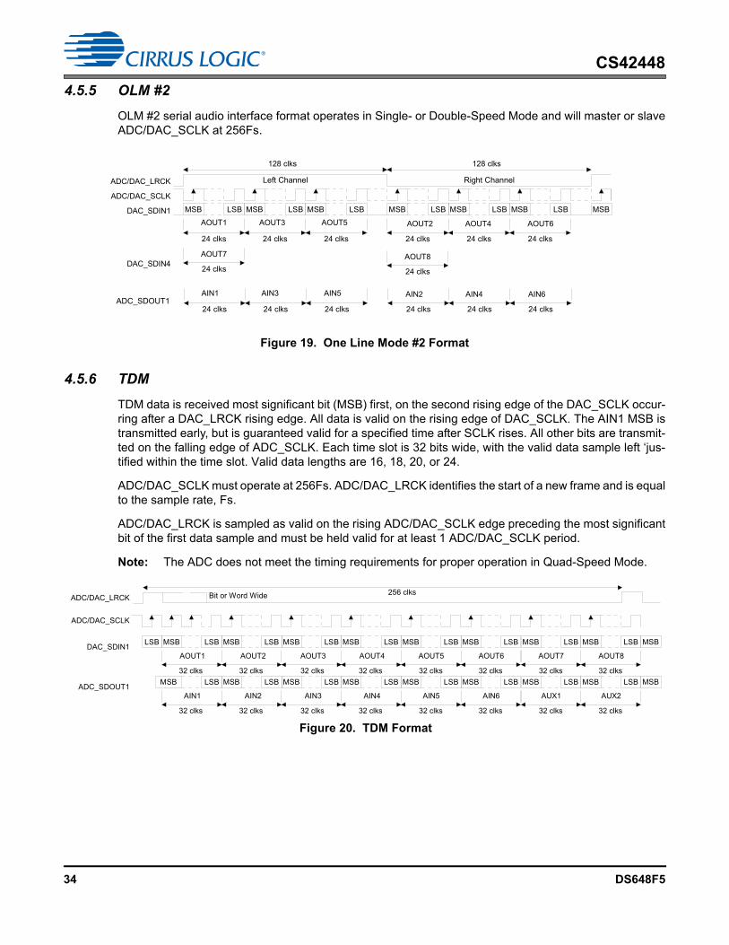
CS42448
4.5.5 OLM #2
OLM #2 serial audio interface format operates in Single- or Double-Speed Mode and will master or slaveADC/DAC_SCLK at 256Fs.
4.5.6 TDM
TDM data is received most significant bit (MSB) first, on the second rising edge of the DAC_SCLK occur-ring after a DAC_LRCK rising edge. All data is valid on the rising edge of DAC_SCLK. The AIN1 MSB istransmitted early, but is guaranteed valid for a specified time after SCLK rises. All other bits are transmit-ted on the falling edge of ADC_SCLK. Each time slot is 32 bits wide, with the valid data sample left ‘jus-tified within the time slot. Valid data lengths are 16, 18, 20, or 24.
ADC/DAC_SCLK must operate at 256Fs. ADC/DAC_LRCK identifies the start of a new frame and is equalto the sample rate, Fs.
ADC/DAC_LRCK is sampled as valid on the rising ADC/DAC_SCLK edge preceding the most significantbit of the first data sample and must be held valid for at least 1 ADC/DAC_SCLK period.
Note: The ADC does not meet the timing requirements for proper operation in Quad-Speed Mode.
Figure 19. One Line Mode #2 Format
ADC/DAC_LRCK
ADC/DAC_SCLK
LSBMSB
24 clks
128 clks
LSBMSB LSBMSB LSBMSB LSBMSB LSBMSB MSB
24 clks 24 clks 24 clks 24 clks 24 clks
Left Channel Right Channel
24 clks
AIN1
24 clks 24 clks 24 clks 24 clks 24 clksADC_SDOUT1
DAC_SDIN1
24 clks
AOUT7
AOUT1 AOUT3 AOUT5 AOUT2 AOUT4 AOUT6
24 clks
AOUT8DAC_SDIN4
AIN3 AIN5 AIN2 AIN4 AIN6
128 clks
AOUT6
ADC/DAC_SCLK
LSBMSB LSBMSB LSBMSB LSBMSB LSBMSB LSBMSBDAC_SDIN1
AOUT1 AOUT4AOUT2 AOUT5AOUT3
32 clks 32 clks 32 clks 32 clks 32 clks 32 clks
AOUT8
LSBMSB LSBMSB
AOUT7
32 clks 32 clks
ADC/DAC_LRCK256 clks
MSB
Bit or Word Wide
LSB
AIN6
LSBMSB LSBMSB LSBMSB LSBMSB LSBMSB LSBMSBADC_SDOUT1
AIN1 AIN4AIN2 AIN5AIN3
32 clks 32 clks 32 clks 32 clks 32 clks 32 clks
AUX2
LSBMSB LSBMSB
AUX1
32 clks 32 clks
MSB
Figure 20. TDM Format
34 DS648F5

CS42448
4.5.7 I/O Channel Allocation
4.6 AUX Port Digital Interface Formats
These serial data lines are used when supporting the TDM Mode of operation with an external ADC or S/PDIF receiver attached. The AUX serial port operates only as a clock master. The AUX_SCLK will operateat 64xFs, where Fs is equal to the ADC sample rate (ADC_LRCK). If the AUX_SDIN signal is not beingused, it should be tied to AGND via a pull-down resistor.
The AUX port will operate in either the Left-Justified or I²S digital interface format with bit depths rangingfrom 16 to 24 bits. Settings for the AUX port are made through the register “Interface Formats (Address04h)” on page 45.
4.6.1 I²S
Digital Input/OutputInterface Format
Analog Output/Input Channel Allocation from/to Digital I/O
DAC_SDIN1I²S, LJ, RJOLMTDM
AOUT 1,2AOUT 1,2,3,4,5,6AOUT 1,2,3,4,5,6,7,8
DAC_SDIN2I²S, LJ, RJOLMTDM
AOUT 3,4Not UsedNot Used
DAC_SDIN3I²S, LJ, RJOLMTDM
AOUT 5,6Not UsedNot Used
DAC_SDIN4I²S, LJ, RJOLMTDM
AOUT 7,8AOUT 7,8Not Used
ADC_SDOUT1I²S, LJ, RJOLMTDM
AIN 1,2AIN 1,2,3,4,5,6AIN 1,2,3,4,5,6; (2 additional channels from AUX_SDIN)
ADC_SDOUT2I²S, LJ, RJOLMTDM
AIN 3,4Not UsedNot Used
ADC_SDOUT3I²S, LJ, RJOLMTDM
AIN 5,6Not UsedNot Used
Table 9. Serial Audio Interface Channel Allocations
AUX_LRCK
AUX_SCLK
M S B LS B M S B LS B
AUX1
Left C hannel Right C han nel
AUX_SDIN
AUX2
MSB
Figure 21. AUX I²S Format
DS648F5 35

CS42448
4.6.2 Left-Justified
4.7 Control Port Description and Timing
The control port is used to access the registers allowing the CS42448 to be configured for the desired op-erational modes and formats. The operation of the control port may be completely asynchronous with re-spect to the audio sample rates. However, to avoid potential interference problems, the control port pinsshould remain static if no operation is required.
The control port has two modes: SPI and I²C, with the CS42448 acting as a slave device. SPI Mode is se-lected if there is a high-to-low transition on the AD0/CS pin, after the RST pin has been brought high. I²CMode is selected by connecting the AD0/CS pin through a resistor to VLC or DGND, thereby permanentlyselecting the desired AD0 bit address state.
4.7.1 SPI Mode
In SPI Mode, CS is the CS42448 chip-select signal, CCLK is the control port bit clock (input into theCS42448 from the microcontroller), CDIN is the input data line from the microcontroller, CDOUT is theoutput data line to the microcontroller. Data is clocked in on the rising edge of CCLK and out on the fallingedge.
Figure 23 shows the operation of the control port in SPI Mode. To write to a register, bring CS low. Thefirst seven bits on CDIN form the chip address and must be 1001111. The eighth bit is a read/write indi-cator (R/W), which should be low to write. The next eight bits form the Memory Address Pointer (MAP),which is set to the address of the register that is to be updated. The next eight bits are the data which willbe placed into the register designated by the MAP. During writes, the CDOUT output stays in the Hi-Zstate. It may be externally pulled high or low with a 47 k resistor, if desired.
There is a MAP auto-increment capability, enabled by the INCR bit in the MAP register. If INCR is a zero,the MAP will stay constant for successive read or writes. If INCR is set to a 1, the MAP will auto-incrementafter each byte is read or written, allowing block reads or writes of successive registers.
To read a register, the MAP has to be set to the correct address by executing a partial write cycle whichfinishes (CS high) immediately after the MAP byte. The MAP auto-increment bit (INCR) may be set or not,as desired. To begin a read, bring CS low, send out the chip address and set the read/write bit (R/W) high.The next falling edge of CCLK will clock out the MSB of the addressed register (CDOUT will leave the highimpedance state). If the MAP auto-increment bit is set to 1, the data for successive registers will appearconsecutively.
AUX_LRCK
AUX_SCLK
M S B LS B M S B LS B
AUX1
Left C hannel Right C han nel
AUX_SDIN
AUX2
MSB
Figure 22. AUX Left-Justified Format
36 DS648F5

CS42448
4.7.2 I²C Mode
In I²C Mode, SDA is a bidirectional data line. Data is clocked into and out of the part by the clock, SCL.There is no CS pin. Pins AD0 and AD1 form the two least-significant bits of the chip address and shouldbe connected through a resistor to VLC or DGND as desired. The state of the pins is sensed while theCS42448 is being reset.
The signal timings for a read and write cycle are shown in Figure 24 and Figure 25. A Start condition isdefined as a falling transition of SDA while the clock is high. A Stop condition is a rising transition whilethe clock is high. All other transitions of SDA occur while the clock is low. The first byte sent to theCS42448 after a Start condition consists of a 7-bit chip address field and a R/W bit (high for a read, lowfor a write). The upper 5 bits of the 7-bit address field are fixed at 10010. To communicate with a CS42448,the chip address field, which is the first byte sent to the CS42448, should match 10010 followed by thesettings of the AD1 and AD0. The eighth bit of the address is the R/W bit. If the operation is a write, thenext byte is the Memory Address Pointer (MAP) which selects the register to be read or written. If the op-eration is a read, the contents of the register pointed to by the MAP will be output. Setting the auto-incre-ment bit in MAP allows successive reads or writes of consecutive registers. Each byte is separated by anacknowledge bit. The ACK bit is output from the CS42448 after each input byte is read, and is input to theCS42448 from the microcontroller after each transmitted byte.
M A P
MSB LSB
DATA
b y te 1 b y te n
R/W R/W
A D D R E S SC H IP
ADDRESSC H IP
C D IN
C C L K
CS
C D O U T MSB LSB MSB LSB
10011111001111
MAP = Memory Address Pointer, 8 bits, MSB first
High Impedance
Figure 23. Control Port Timing in SPI Mode
4 5 6 7 24 25
SCL
CHIP ADDRESS (WRITE) MAP BYTE DATA DATA +1
START
ACK
STOP
ACKACKACK
1 0 0 1 0 AD1 AD0 0SDA INCR 6 5 4 3 2 1 0 7 6 1 0 7 6 1 0 7 6 1 0
0 1 2 3 8 9 12 16 17 18 1910 11 13 14 15 27 2826
DATA +n
Figure 24. Control Port Timing, I²C Write
DS648F5 37

CS42448
Since the read operation cannot set the MAP, an aborted write operation is used as a preamble. As shownin Figure 25, the write operation is aborted after the acknowledge for the MAP byte by sending a stop con-dition. The following pseudocode illustrates an aborted write operation followed by a read operation.
Send start condition.
Send 10010xx0 (chip address & write operation).
Receive acknowledge bit.
Send MAP byte, auto increment off.
Receive acknowledge bit.
Send stop condition, aborting write.
Send start condition.
Send 10010xx1(chip address & read operation).
Receive acknowledge bit.
Receive byte, contents of selected register.
Send acknowledge bit.
Send stop condition.
Setting the auto-increment bit in the MAP allows successive reads or writes of consecutive registers. Eachbyte is separated by an acknowledge bit.
4.8 Interrupts
The CS42448 has a comprehensive interrupt capability. The INT output pin is intended to drive the interruptinput pin on the host microcontroller. The INT pin may be configured as an active low or active high CMOSdriver or an open-drain driver. This last mode is used for active low, wired-OR hook-ups, with multiple pe-ripherals connected to the microcontroller interrupt input pin.
Many conditions can cause an interrupt, as listed in the interrupt status register descriptions. See “Status(Address 19h) (Read Only)” on page 52. Each source may be masked off through mask register bits. In ad-dition, each source may be set to rising edge, falling edge, or level sensitive. Combined with the option oflevel sensitive or edge sensitive modes within the microcontroller, many different configurations are possi-ble, depending on the needs of the system designer.
SCL
CHIP ADDRESS (WRITE) MAP BYTE DATA DATA +1
START
ACK
STOPACKACKACK
1 0 0 1 0 AD1 AD0 0SDA 1 0 0 1 0 AD1 AD0 1
CHIP ADDRESS (READ)
START
INCR 6 5 4 3 2 1 0 7 0 7 0 7 0
NO
168 9 12 13 14 154 5 6 7 0 1 20 21 22 23 24 26 27 282 3 10 11 17 18 19 25
ACK
DATA + nSTOP
Figure 25. Control Port Timing, I²C Read
38 DS648F5

CS42448
4.9 Recommended Power-Up Sequence1. Hold RST low until the power supply and clocks are stable. In this state, the control port is reset to its
default settings and VQ will remain low.
2. Bring RST high. The device will initially be in a low power state with VQ low. All features will default asdescribed in the “Register Quick Reference” on page 40.
3. Perform a write operation to the Power Control register (“Power Control (Address 02h)” on page 43) toset bit 0 to a ‘1’b. This will place the device in a power down state.
4. Load the desired register settings while keeping the PDN bit set to ‘1’b.
5. Mute all DACs. Muting the DACs suppresses any noise associated with the CODEC's first initializationafter power is applied.
6. Set the PDN bit in the power control register to ‘0’b. VQ will ramp to approximately VA/2 according tothe Popguard specification in section “Popguard” on page 29.
7. Following approximately 2000 LRCK cycles, the device is initialized and ready for normal operation.
8. After the CODEC is initialized, wait ~90 LRCK cycles (~1.9 ms @48 kHz) and then un-mute the DACs.
9. Normal operation begins.
4.10 Reset and Power-Up
It is recommended that reset be activated if the analog or digital supplies drop below the recommended op-erating condition to prevent power-glitch-related issues.
The delta-sigma modulators settle in a matter of microseconds after the analog section is powered, eitherthrough the application of power or by setting the RST pin high. However, the voltage reference will takemuch longer to reach a final value due to the presence of external capacitance on the ADC/DAC_FILT+pins. A time delay of approximately 400 ms is required after applying power to the device or after exiting areset state. During this voltage reference ramp delay, all serial ports and DAC outputs will be automaticallymuted.
4.11 Power Supply, Grounding, and PCB Layout
As with any high-resolution converter, the CS42448 requires careful attention to power supply and ground-ing arrangements if its potential performance is to be realized. Figure 2 shows the recommended power ar-rangements, with VA connected to clean supplies. VD, which powers the digital circuitry, may be run fromthe system logic supply. Alternatively, VD may be powered from the analog supply via a ferrite bead. In thiscase, no additional devices should be powered from VD.
Extensive use of power and ground planes, ground plane fill in unused areas and surface mount decouplingcapacitors are recommended. Decoupling capacitors should be placed as close to the pins of the CS42448as possible. The low value ceramic capacitor should be closest to the pin and should be mounted on thesame side of the board as the CS42448 to minimize inductance effects. All signals, especially clocks, shouldbe kept away from the ADC/DAC_FILT+, VQ pins in order to avoid unwanted coupling into the modulators.The ADC/DAC_FILT+ and VQ decoupling capacitors, particularly the 0.1 µF, must be positioned to mini-mize the electrical path from ADC/DAC_FILT+ and AGND. The CS42448 evaluation board demonstratesthe optimum layout and power supply arrangements.
For optimal heat dissipation from the package, it is recommended that the area directly under the part befilled with copper and tied to the ground plane. The use of vias connecting the topside ground to the back-side ground is also recommended.
DS648F5 39
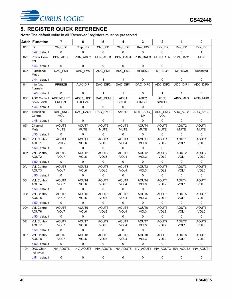
CS42448
5. REGISTER QUICK REFERENCENote: The default value in all “Reserved” registers must be preserved.
Addr Function 7 6 5 4 3 2 1 0
01h ID Chip_ID3 Chip_ID2 Chip_ID1 Chip_ID0 Rev_ID3 Rev_ID2 Rev_ID1 Rev_ID0
p 42 default 0 0 0 0 0 0 0 1
02h Power Con-trol
PDN_ADC3 PDN_ADC2 PDN_ADC1 PDN_DAC4 PDN_DAC3 PDN_DAC2 PDN_DAC1 PDN
p 43 default 0 0 0 0 0 0 0 0
03h Functional Mode
DAC_FM1 DAC_FM0 ADC_FM1 ADC_FM0 MFREQ2 MFREQ1 MFREQ0 Reserved
p 44 default 1 1 1 1 0 0 0 0
04h Interface Formats
FREEZE AUX_DIF DAC_DIF2 DAC_DIF1 DAC_DIF0 ADC_DIF2 ADC_DIF1 ADC_DIF0
p 45 default 0 0 1 1 0 1 1 0
05h ADC Control(w/DAC_DEM)
ADC1-2_HPF FREEZE
ADC3_HPF FREEZE
DAC_DEM ADC1SINGLE
ADC2SINGLE
ADC3SINGLE
AIN5_MUX AIN6_MUX
p 46 default 0 0 0 0 0 0 0 0
06h Transition Control
DAC_SNGVOL
DAC_SZC1 DAC_SZC0 AMUTE MUTE ADC_SP
ADC_SNGVOL
ADC_SZC1 ADC_SZC0
p 48 default 0 0 0 1 0 0 0 0
07h Channel Mute
AOUT8 MUTE
AOUT7 MUTE
AOUT6 MUTE
AOUT5 MUTE
AOUT4 MUTE
AOUT3 MUTE
AOUT2 MUTE
AOUT1 MUTE
p 50 default 0 0 0 0 0 0 0 0
08h Vol. Control AOUT1
AOUT1 VOL7
AOUT1 VOL6
AOUT1 VOL5
AOUT1 VOL4
AOUT1 VOL3
AOUT1 VOL2
AOUT1 VOL1
AOUT1 VOL0
p 50 default 0 0 0 0 0 0 0 0
09h Vol. Control AOUT2
AOUT2 VOL7
AOUT2 VOL6
AOUT2 VOL5
AOUT2 VOL4
AOUT2 VOL3
AOUT2VOL2
AOUT2 VOL1
AOUT2 VOL0
p 50 default 0 0 0 0 0 0 0 0
0Ah Vol. Control AOUT3
AOUT3 VOL7
AOUT3 VOL6
AOUT3 VOL5
AOUT3 VOL4
AOUT3 VOL3
AOUT3 VOL2
AOUT3 VOL1
AOUT3 VOL0
p 50 default 0 0 0 0 0 0 0 0
0Bh Vol. Control AOUT4
AOUT4 VOL7
AOUT4 VOL6
AOUT4 VOL5
AOUT4 VOL4
AOUT4 VOL3
AOUT4 VOL2
AOUT4 VOL1
AOUT4 VOL0
p 50 default 0 0 0 0 0 0 0 0
0Ch Vol. Control AOUT5
AOUT5 VOL7
AOUT5 VOL6
AOUT5 VOL5
AOUT5 VOL4
AOUT5 VOL3
AOUT5 VOL2
AOUT5 VOL1
AOUT5 VOL0
p 50 default 0 0 0 0 0 0 0 0
0Dh Vol. Control AOUT6
AOUT6 VOL7
AOUT6 VOL6
AOUT6 VOL5
AOUT6 VOL4
AOUT6 VOL3
AOUT6 VOL2
AOUT6 VOL1
AOUT6 VOL0
p 50 default 0 0 0 0 0 0 0 0
0Eh Vol. Control AOUT7
AOUT7 VOL7
AOUT7 VOL6
AOUT7 VOL5
AOUT7 VOL4
AOUT7 VOL3
AOUT7 VOL2
AOUT7 VOL1
AOUT7 VOL0
p 50 default 0 0 0 0 0 0 0 0
0Fh Vol. Control AOUT8
AOUT8 VOL7
AOUT8 VOL6
AOUT8 VOL5
AOUT8 VOL4
AOUT8 VOL3
AOUT8 VOL2
AOUT8 VOL1
AOUT8 VOL0
p 50 default 0 0 0 0 0 0 0 0
10h DAC Chan-nel Invert
INV_AOUT8 INV_AOUT7 INV_AOUT6 INV_AOUT5 INV_AOUT4 INV_AOUT3 INV_AOUT2 INV_AOUT1
p 51 default 0 0 0 0 0 0 0 0
40 DS648F5

CS42448
11h Vol. ControlAIN1
AIN1VOL7
AIN1VOL6
AIN1VOL5
AIN1VOL4
AIN1VOL3
AIN1VOL2
AIN1VOL1
AIN1VOL0
p 50 default 0 0 0 0 0 0 0 0
12h Vol. ControlAIN2
AIN2VOL7
AIN2VOL6
AIN2VOL5
AIN2VOL4
AIN2VOL3
AIN2VOL2
AIN2VOL1
AIN2VOL0
p 51 default 0 0 0 0 0 0 0 0
13h Vol. ControlAIN3
AIN3VOL7
AIN3VOL6
AIN3VOL5
AIN3VOL4
AIN3VOL3
AIN3VOL2
AIN3VOL1
AIN3VOL0
p 50 default 0 0 0 0 0 0 0 0
14h Vol. ControlAIN4
AIN4VOL7
AIN4VOL6
AIN4VOL5
AIN4VOL4
AIN4VOL3
AIN4VOL2
AIN4VOL1
AIN4VOL0
p 51 default 0 0 0 0 0 0 0 0
15h Vol. ControlAIN5
AIN5VOL7
AIN5VOL6
AIN5VOL5
AIN5VOL4
AIN5VOL3
AIN5VOL2
AIN5VOL1
AIN5VOL0
p 50 default 0 0 0 0 0 0 0 0
16h Vol. ControlAIN6
AIN6VOL7
AIN6VOL6
AIN6VOL5
AIN6VOL4
AIN6VOL3
AIN6VOL2
AIN6VOL1
AIN6VOL0
p 51 default 0 0 0 0 0 0 0 0
17h ADC Chan-nel Invert
Reserved Reserved INV_A6 INV_A5 INV_A4 INV_A3 INV_A2 INV_A1
p 51 default 0 0 0 0 0 0 0 0
18h Status Con-trol
Reserved Reserved Reserved Reserved INT1 INT0 Reserved Reserved
p 52 default 0 0 0 0 0 0 0 0
19h Status Reserved Reserved Reserved DAC_CLKError
ADC_CLKError
ADC3OVFL
ADC2OVFL
ADC1OVFL
p 52 default 0 0 0 X X X X X
1Ah Status Mask Reserved Reserved Reserved DAC_CLKError_M
ADC_CLKError_M
ADC3 OVFL_M
ADC2 OVFL_M
ADC1 OVFL_M
p 53 default 0 0 0 0 0 0 0 0
1Bh MUTEC Reserved Reserved Reserved Reserved Reserved Reserved MCPolarity MUTEC Active
p 53 default 0 0 0 0 0 0 0 0
Addr Function 7 6 5 4 3 2 1 0
DS648F5 41
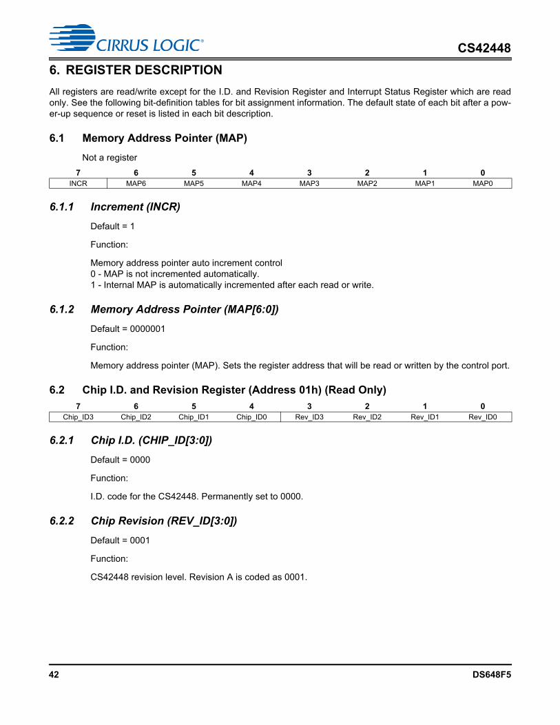
CS42448
6. REGISTER DESCRIPTION
All registers are read/write except for the I.D. and Revision Register and Interrupt Status Register which are readonly. See the following bit-definition tables for bit assignment information. The default state of each bit after a pow-er-up sequence or reset is listed in each bit description.
6.1 Memory Address Pointer (MAP)
Not a register
6.1.1 Increment (INCR)
Default = 1
Function:
Memory address pointer auto increment control0 - MAP is not incremented automatically.1 - Internal MAP is automatically incremented after each read or write.
6.1.2 Memory Address Pointer (MAP[6:0])
Default = 0000001
Function:
Memory address pointer (MAP). Sets the register address that will be read or written by the control port.
6.2 Chip I.D. and Revision Register (Address 01h) (Read Only)
6.2.1 Chip I.D. (CHIP_ID[3:0])
Default = 0000
Function:
I.D. code for the CS42448. Permanently set to 0000.
6.2.2 Chip Revision (REV_ID[3:0])
Default = 0001
Function:
CS42448 revision level. Revision A is coded as 0001.
7 6 5 4 3 2 1 0INCR MAP6 MAP5 MAP4 MAP3 MAP2 MAP1 MAP0
7 6 5 4 3 2 1 0Chip_ID3 Chip_ID2 Chip_ID1 Chip_ID0 Rev_ID3 Rev_ID2 Rev_ID1 Rev_ID0
42 DS648F5

CS42448
6.3 Power Control (Address 02h)
6.3.1 Power Down ADC Pairs (PDN_ADCX)
Default = 0
0 - Disable1 - Enable
Function:
When enabled, the respective ADC channel pair (ADC1 - AIN1/AIN2; ADC2 - AIN3/AIN4; and ADC3 -AIN5/AIN6) will remain in a reset state.
6.3.2 Power Down DAC Pairs (PDN_DACX)
Default = 0
0 - Disable1 - Enable
Function:
When enabled, the respective DAC channel pair (DAC1 - AOUT1/AOUT2; DAC2 - AOUT3/AOUT4; DAC3- AOUT5/AOUT6; and DAC4 - AOUT7/AOUT8) will remain in a reset state. It is advised that any changeof these bits be made while the DACs are muted or the power down bit (PDN) is enabled to eliminate thepossibility of audible artifacts.
6.3.3 Power Down (PDN)
Default = 0
0 - Disable1 - Enable
Function:
The entire device will enter a low-power state when this function is enabled. The contents of the controlregisters are retained in this mode.
7 6 5 4 3 2 1 0PDN_ADC3 PDN_ADC2 PDN_ADC1 PDN_DAC4 PDN_DAC3 PDN_DAC2 PDN_DAC1 PDN
DS648F5 43

CS42448
6.4 Functional Mode (Address 03h)
6.4.1 DAC Functional Mode (DAC_FM[1:0])
Default = 11
Master Mode00 - Single-Speed Mode (4 to 50 kHz sample rates)01 - Double-Speed Mode (50 to 100 kHz sample rates)10 - Quad-Speed Mode (100 to 200 kHz sample rates)
Slave Mode11 - (Auto-detect sample rates)
Function:
Selects the required range of sample rates for the DAC serial port.
6.4.2 ADC Functional Mode (ADC_FM[1:0])
Default = 11
Master Mode00 - Single-Speed Mode (4 to 50 kHz sample rates)01 - Double-Speed Mode (50 to 100 kHz sample rates)10 - Quad-Speed Mode (100 to 200 kHz sample rates)
Slave Mode11 - (Auto-detect sample rates)
Function:
Selects the required range of sample rates for the ADC serial port.
6.4.3 MCLK Frequency (MFREQ[2:0])
Default = 000
Function:
Sets the appropriate frequency for the supplied MCLK. For TDM and OLM #2 operation, ADC/DAC_SCLKmust equal 256Fs. For OLM #1 operation, ADC/DAC_SCLK must equal 128Fs. MCLK can be equal to orgreater than the higher frequency of ADC_SCLK or DAC_SCLK.
7 6 5 4 3 2 1 0
DAC_FM1 DAC_FM0 ADC_FM1 ADC_FM0 MFreq2 MFreq1 MFreq0 Reserved
Ratio (xFs)
MFreq2 MFreq1 MFreq0 Description SSM DSM QSM0 0 0 1.0290 MHz to 12.8000 MHz 256 128 640 0 1 Reserved0 1 0 2.0480 MHz to 25.6000 MHz 512 256 1280 1 1 Reserved1 X X 4.0960 MHz to 51.2000 MHz 1024 512 256
Table 10. MCLK Frequency Settings for I²S, Left and Right Justified Interface Formats
44 DS648F5

CS42448
6.5 Interface Formats (Address 04h)
6.5.1 Freeze Controls (FREEZE)
Default = 0
Function:
This function will freeze the previous settings of, and allow modifications to be made to the channel mutes,the DAC and ADC Volume Control/Channel Invert registers without the changes taking effect until theFREEZE is disabled. To have multiple changes in these control port registers take effect simultaneously,enable the FREEZE bit, make all register changes, then disable the FREEZE bit.
6.5.2 Auxiliary Digital Interface Format (AUX_DIF)
Default = 0
0 - Left Justified1 - I²S
Function:
This bit selects the digital interface format used for the AUX Serial Port. The required relationship betweenthe Left/Right clock, serial clock and serial data is defined by the Digital Interface Format and the optionsare detailed in Figures 23-24.
6.5.3 DAC Digital Interface Format (DAC_DIF[2:0])
Default = 110
Function:
These bits select the digital interface format used for the DAC Serial Port. The required relationship betweenthe Left/Right clock, serial clock and serial data is defined by the Digital Interface Format; the options aredetailed in the section “CODEC Digital Interface Formats” on page 32.
Refer to Table 9, “Serial Audio Interface Channel Allocations,” on page 35.
Ratio (xFs)
MFreq2 MFreq1 MFreq0 Description SSM DSM QSM0 0 0 1.0290 MHz to 12.8000 MHz 256 N/A N/A0 0 1 Reserved0 1 0 2.0480 MHz to 25.6000 MHz 512 256 N/A0 0 1 Reserved1 X X 4.0960 MHz to 51.2000 MHz 1024 512 256
Table 11. MCLK Frequency Settings for TDM & OLM Interface Formats
7 6 5 4 3 2 1 0FREEZE AUX_DIF DAC_DIF2 DAC_DIF1 DAC_DIF0 ADC_DIF2 ADC_DIF1 ADC_DIF0
DAC_DIF2 DAC_DIF1 DAC_DIF0 Description Format Figure0 0 0 Left Justified, up to 24-bit data 0 Figure 16
0 0 1 I²S, up to 24-bit data 1 Figure 15
0 1 0 Right Justified, 24-bit data 2 Figure 17
Table 12. DAC Digital Interface Formats
DS648F5 45

CS42448
6.5.4 ADC Digital Interface Format (ADC_DIF[2:0])
Default = 110
Function:
These bits select the digital interface format used for the ADC serial port. The required relationship betweenthe Left/Right clock, serial clock and serial data is defined by the Digital Interface Format and the optionsare detailed in the section “CODEC Digital Interface Formats” on page 32. Refer to Table 9, “Serial AudioInterface Channel Allocations,” on page 35.
Note: The ADC does not meet Quad-Speed Mode timing specifications in the TDM interface format.
6.6 ADC Control & DAC De-Emphasis (Address 05h)
6.6.1 ADC1-2 High-Pass Filter Freeze (ADC1-2_HPF FREEZE)
Default = 0
Function:
When this bit is set, the internal high-pass filter will be disabled for ADC1 and ADC2.The current DC offsetvalue will be frozen and continue to be subtracted from the conversion result. See “ADC Digital FilterCharacteristics” on page 13.
0 1 1 Right Justified, 16-bit data 3 Figure 17
1 0 0 One-Line #1, 20-bit 4 Figure 18
1 0 1 One-Line #2, 24-bit 5 Figure 19
1 1 0 TDM Mode, 24-bit (slave only) 6 Figure 20
1 1 1 Reserved - -
ADC_DIF2 ADC_DIF1 ADC_DIF0 Description Format Figure0 0 0 Left Justified, up to 24-bit data 0 Figure 16
0 0 1 I²S, up to 24-bit data 1 Figure 15
0 1 0 Right Justified, 24-bit data 2 Figure 17
0 1 1 Right Justified, 16-bit data 3 Figure 17
1 0 0 One-Line #1, 20-bit 4 Figure 18
1 0 1 One-Line #2, 24-bit 5 Figure 19
1 1 0 TDM Mode, 24-bit (slave only) 6 Figure 20
1 1 1 Reserved - -
Table 13. ADC Digital Interface Formats
7 6 5 4 3 2 1 0ADC1-2_HPF
FREEZEADC3_HPF
FREEZEDAC_DEM ADC1
SINGLEADC2
SINGLEADC3
SINGLEAIN5_MUX AIN6_MUX
DAC_DIF2 DAC_DIF1 DAC_DIF0 Description Format Figure
Table 12. DAC Digital Interface Formats
46 DS648F5

CS42448
6.6.2 ADC3 High Pass Filter Freeze (ADC3_HPF FREEZE)
Default = 0
Function:
When this bit is set, the internal high-pass filter will be disabled for ADC3.The current DC offset value willbe frozen and continue to be subtracted from the conversion result. See “ADC Digital Filter Characteris-tics” on page 13.
6.6.3 DAC De-Emphasis Control (DAC_DEM)
Default = 0
0 - No De-Emphasis1 - De-Emphasis Enabled (Auto-Detect Fs)
Function:
Enables the digital filter to maintain the standard 15s/50s digital de-emphasis filter response at the au-to-detected sample rate of either 32, 44.1, or 48 kHz. De-emphasis will not be enabled, regardless of thisregister setting, at any other sample rate.
6.6.4 ADC1 Single-Ended Mode (ADC1 SINGLE)
Default = 0
0 - Disabled; Differential input to ADC11 - Enabled; Single-Ended input to ADC1
Function:
When enabled, this bit allows the user to apply a single-ended input to the positive terminal of ADC1. A+6 dB digital gain is automatically applied to the serial audio data of ADC1. The negative leg must be driv-en to the common mode of the ADC. See Figure 27 on page 54 for a graphical description, and Sections4.2.1 and 6.14.3.
6.6.5 ADC2 Single-Ended Mode (ADC2 SINGLE)
Default = 0
0 - Disabled; Differential input to ADC21 - Enabled; Single-Ended input to ADC2
Function:
When enabled, this bit allows the user to apply a single-ended input to the positive terminal of ADC2. A+6 dB digital gain is automatically applied to the serial audio data of ADC2. The negative leg must be driv-en to the common mode of the ADC. See Figure 27 on page 54 for a graphical description, and Sections4.2.1 and 6.14.3.
DS648F5 47

CS42448
6.6.6 ADC3 Single-Ended Mode (ADC3 SINGLE)
Default = 0
0 - Disabled; Differential input to ADC1 - Enabled; Single-Ended input to ADC
Function:
When disabled, this bit removes the 4:2 multiplexer from the signal path of ADC3 allowing a differentialinput. When enabled, this bit allows the user to choose between four single-ended inputs to ADC3, usingthe AIN5_MUX and AIN6_MUX bits. See Figure 27 on page 54 for a graphical description, and Sections4.2.1 and 6.14.3.
6.6.7 Analog Input Ch. 5 Multiplexer (AIN5_MUX)
Default = 0
0 - Single-Ended Input AIN5A1 - Single-Ended Input AIN5B
Function:
ADC3 can accept single-ended input signals when the ADC3 SINGLE bit is enabled. The AIN5_MUX bitselects between two input channels (AIN5A or AIN5B) to be sent to ADC3 in Single-Ended Mode. This bitis ignored when the ADC3_SINGLE bit is disabled. See Figure 27 on page 54 for a graphical description,and Sections 4.2.1 and 6.14.3.
6.6.8 Analog Input Ch. 6 Multiplexer (AIN6_MUX)
Default = 0
0 - Single-Ended Input AIN6A1 - Single-Ended Input AIN6B
Function:
ADC3 can accept a single-ended input signal when the ADC3 SINGLE bit is enabled. The AIN6_MUX bitselects between two input channels (AIN6A or AIN6B) to be sent to ADC3 in Single-Ended Mode. This bitis ignored when the ADC3_SINGLE bit is disabled. See Figure 27 on page 54 for a graphical description,and Sections 4.2.1 and 6.14.3.
6.7 Transition Control (Address 06h)
6.7.1 Single Volume Control (DAC_SNGVOL, ADC_SNGVOL)
Default = 0
Function:
The individual channel volume levels are independently controlled by their respective Volume Control reg-isters when this function is disabled. When enabled, the volume on all channels is determined by theAOUT1 and AIN1 Volume Control register and the other Volume Control registers are ignored.
7 6 5 4 3 2 1 0DAC_SNGVOL DAC_SZC1 DAC_SZC0 AMUTE MUTE ADC_SP ADC_SNGVOL ADC_SZC1 ADC_SZC0
48 DS648F5

CS42448
6.7.2 Soft Ramp and Zero Cross Control (ADC_SZC[1:0], DAC_SZC[1:0])
Default = 00
00 - Immediate Change01 - Zero Cross 10 - Soft Ramp11 - Soft Ramp on Zero Crossings
Function:
Immediate Change
When Immediate Change is selected, all volume-level changes will take effect immediately in one step.
Zero Cross
Zero Cross Enable dictates that signal level changes, either by gain changes, attenuation changes or mut-ing, will occur on a signal zero crossing to minimize audible artifacts. The requested level change will oc-cur after a timeout period between 512 and 1024 sample periods (10.7 ms to 21.3 ms at 48 kHz samplerate) if the signal does not encounter a zero crossing. The zero cross function is independently monitoredand implemented for each channel.
Soft Ramp
Soft Ramp allows level changes, either by gain changes, attenuation changes or muting, to be implement-ed by incrementally ramping, in 1/8 dB steps, from the current level to the new level at a rate of 1 dB per8 left/right clock periods.
Soft Ramp on Zero Crossing
Soft Ramp and Zero Cross Enable dictates that signal level changes, either by gain changes, attenuationchanges or muting, will occur in 1/8 dB steps and be implemented on a signal zero crossing. The 1/8 dBlevel change will occur after a timeout period between 512 and 1024 sample periods (10.7 ms to 21.3 msat 48 kHz sample rate) if the signal does not encounter a zero crossing. The zero cross function is inde-pendently monitored and implemented for each channel.
6.7.3 Auto-Mute (AMUTE)
Default = 1
0 - Disabled1 - Enabled
Function:
The Digital-to-Analog converters of the CS42448 will mute the output following the reception of 8192 con-secutive audio samples of static 0 or -1. A single sample of non-static data will release the mute. Detectionand muting is done independently for each channel. The quiescent voltage on the output will be retainedand the MUTEC pin will go active during the mute period. The muting function is affected, similar to vol-ume control changes, by the Soft and Zero Cross bits (SZC[1:0]).
DS648F5 49

CS42448
6.7.4 Mute ADC Serial Port (MUTE ADC_SP)
Default = 0
0 - Disabled1 - Enabled
Function:
When enabled, the ADC Serial Port will be muted.
6.8 DAC Channel Mute (Address 07h)
6.8.1 Independent Channel Mute (AOUTX_MUTE)
Default = 0
0 - Disabled1 - Enabled
Function:
The respective Digital-to-Analog converter outputs of the CS42448 will mute when enabled. The quies-cent voltage on the outputs will be retained. The muting function is affected by the DAC Soft and ZeroCross bits (DAC_SZC[1:0]). When all channels are muted, the MUTEC pin will become active.
6.9 AOUTX Volume Control (Addresses 08h- 0Fh)
6.9.1 Volume Control (AOUTX_VOL[7:0])
Default = 00h
Function:
The AOUTx Volume Control registers allow independent setting of the signal levels in 0.5 dB incrementsfrom 0 dB to -127.5 dB. Volume settings are decoded as shown in Table 14. The volume changes areimplemented as dictated by the Soft and Zero Cross bits (DAC_SZC[1:0]). All volume settings less than-127.5 dB are equivalent to enabling the AOUTx_MUTE bit for the given channel.
7 6 5 4 3 2 1 0AOUT8_MUTE AOUT7_MUTE AOUT6_MUTE AOUT5_MUTE AOUT4_MUTE AOUT3_MUTE AOUT2_MUTE AOUT1_MUTE
7 6 5 4 3 2 1 0AOUTx_VOL7 AOUTx_VOL6 AOUTx_VOL5 AOUTx_VOL4 AOUTx_VOL3 AOUTx_VOL2 AOUTx_VOL1 AOUTx_VOL0
Binary Code Volume Setting00000000 0 dB00101000 -20 dB01010000 -40 dB01111000 -60 dB10110100 -90 dB
Table 14. Example AOUT Volume Settings
50 DS648F5

CS42448
6.10 DAC Channel Invert (Address 10h)
6.10.1 Invert Signal Polarity (INV_AOUTX)
Default = 0
0 - Disabled1 - Enabled
Function:
When enabled, these bits will invert the signal polarity of their respective channels.
6.11 AINX Volume Control (Address 11h-16h)
6.11.1 AINX Volume Control (AINX_VOL[7:0])
Default = 00h
Function:
The level of AIN1 - AIN6 can be adjusted in 0.5 dB increments as dictated by the ADC Soft and Zero Crossbits (ADC_SZC[1:0]) from +24 to -64 dB. Levels are decoded in two’s complement, as shown in Table 15.
6.12 ADC Channel Invert (Address 17h)
6.12.1 Invert Signal Polarity (INV_AINX)
Default = 0
0 - Disabled1 - Enabled
Function:
When enabled, these bits will invert the signal polarity of their respective channels.
7 6 5 4 3 2 1 0INV_AOUT8 INV_AOUT7 INV_AOUT6 INV_AOUT5 INV_AOUT4 INV_AOUT3 INV_AOUT2 INV_AOUT1
7 6 5 4 3 2 1 0AINx_VOL7 AINx_VOL6 AINx_VOL5 AINx_VOL4 AINx_VOL3 AINx_VOL2 AINx_VOL1 AINx_VOL0
Binary Code Volume Setting0111 1111 +24 dB
··· ···0011 0000 +24 dB
··· ···0000 0000 0 dB1111 1111 -0.5 dB1111 1110 -1 dB
··· ···1000 0000 -64 dB
Table 15. Example AIN Volume Settings
7 6 5 4 3 2 1 0Reserved Reserved INV_AIN6 INV_AIN5 INV_AIN4 INV_AIN3 INV_AIN2 INV_AIN1
DS648F5 51

CS42448
6.13 Status Control (Address 18h)
6.13.1 Interrupt Pin Control (INT[1:0])
Default = 00
00 - Active high; high output indicates interrupt condition has occurred01 - Active low, low output indicates an interrupt condition has occurred10 - Open drain, active low. Requires an external pull-up resistor on the INT pin.11 - Reserved
Function:
Determines how the Interrupt pin (INT) will indicate an interrupt condition.
For DAC and ADC clock errors, the INT pin is set to “Level Active Mode” and will become active duringthe clock error. For the ADCx_OVFL error, the INT pin is set to Level Active Mode and will become activeduring the overflow error.
6.14 Status (Address 19h) (Read Only)
For all bits in this register, a “1” means the associated error condition has occurred at least once since theregister was last read. A”0” means the associated error condition has NOT occurred since the last readingof the register. Reading the register resets all bits to 0. Status bits that are masked off in the associatedmask register will always be “0” in this register.
6.14.1 DAC CLOCK ERROR (DAC_CLK ERROR)
Default = x
Function:
Indicates an invalid MCLK to DAC_LRCK ratio. This status flag is set to “Level Active Mode” and becomesactive during the error condition. See “System Clocking” on page 31 for valid clock ratios.
6.14.2 ADC CLOCK ERROR (ADC_CLK ERROR)
Default = x
Function:
Indicates an invalid MCLK to ADC_LRCK ratio. This status flag is set to “Level Active Mode” and becomesactive during the error condition. See “System Clocking” on page 31 for valid clock ratios.
6.14.3 ADC Overflow (ADCX_OVFL)
Default = x
Function:
Indicates that there is an over-range condition anywhere in the CS42448 ADC signal path of each of theassociated ADCs. This status flag becomes active on the arrival of the error condition. This bit is reservedwhen analog inputs are driven as single-ended.
7 6 5 4 3 2 1 0Reserved Reserved Reserved Reserved INT1 INT0 Reserved Reserved
7 6 5 4 3 2 1 0Reserved Reserved Reserved DAC_CLK Error ADC_CLK Error ADC3_OVFL ADC2_OVFL ADC1_OVFL
52 DS648F5

CS42448
6.15 Status Mask (Address 1Ah)
Default = 00000
Function:
The bits of this register serve as a mask for the error sources found in the register “Status (Address 19h)(Read Only)” on page 52. If a mask bit is set to 1, the error is unmasked, meaning that its occurrence willaffect the INT pin and the status register. If a mask bit is set to 0, the error is masked, meaning that its oc-currence will not affect the INT pin or the status register. The bit positions align with the corresponding bitsin the Status register.
6.16 MUTEC Pin Control (Address 1Bh)
6.17 MUTEC Polarity Select (MCPOLARITY)
Default = 0
0 - Active low1 - Active high
Function:
Determines the polarity of the MUTEC pin.
6.18 MUTE CONTROL ACTIVE (MUTEC ACTIVE)
Default = 0
0 - MUTEC pin is not active.1 - MUTEC pin is active.
Function:
The MUTEC pin will go high or low (depending on the MUTEC Polarity Select bit) when this bit is enabled.
7 6 5 4 3 2 1 0Reserved Reserved Reserved DAC_CLK Error_
MADC_CLK Error_
MADC3_OVFL_M ADC2_OVFL_M ADC1_OVFL_M
7 6 5 4 3 2 1 0Reserved Reserved Reserved Reserved Reserved Reserved MCPolarity MUTEC
ACTIVE
DS648F5 53

CS42448
7. EXTERNAL FILTERS
7.1 ADC Input Filter
The analog modulator samples the input at 6.144 MHz (internal MCLK=12.288 MHz). The digital filter willreject signals within the stopband of the filter. However, there is no rejection for input signals which are mul-tiples of the digital passband frequency (n 6.144 MHz), where n=0,1,2,... Refer to Figures 26 and 27 fora recommended analog input filter that will attenuate any noise energy at 6.144 MHz, in addition to providingthe optimum source impedance for the modulators. Refer to Figures 28 and 29 for low-cost, low-component-count passive input filters. The use of capacitors that have a large voltage coefficient (such as general-pur-pose ceramics) must be avoided since these can degrade signal linearity
VA
+
+
-
-4.7 F
100 k10 k
100 k
100 k
0.1 F 100 F
470 pF
470 pFC0G
C0G
634
634
634
91
91
2700 pFC0G
332
AINx+
AINx-
ADC1-3
Figure 26. Single to Differential Active Input Filter
‐
+
470 pF
C0G
634
91
2700 pFC0G
4.7 F
100 k100 k
100 k
VA
4.7 F
AIN1+,2+,3+,4+
AIN1-,2-,3-,4-
ADC1-2
ADC3‐
+
470 pF
C0G
634
91
2700 pFC0G
4.7 F
100 k100 k
100 k
VA
AIN5A,6A
‐
+
470 pF
C0G
634
91
2700 pFC0G
4.7 F
100 k100 k
100 k
VA
AIN5B,6B
Figure 27. Single-Ended Active Input Filter
54 DS648F5

CS42448
7.1.1 Passive Input Filter
The passive filter implementation shown in Figure 28 will attenuate any noise energy at 6.144 MHz butwill not provide optimum source impedance for the ADC modulators. Full analog performance will there-fore not be realized using a passive filter. Figure 28 illustrates the unity gain, passive input filter solution.In this topology the distortion performance is affected, but the dynamic range performance is not limited.
7.1.2 Passive Input Filter w/Attenuation
Some applications may require signal attenuation prior to the ADC. The full-scale input voltage will scalewith the analog power supply voltage. For VA = 5.0 V, the full-scale input voltage is approximately2.8 Vpp, or 1 Vrms (most consumer audio line-level outputs range from 1.5 to 2 Vrms).
Figure 29 shows a passive input filter with 6 dB of signal attenuation. Due to the relatively high input im-pedance on the analog inputs, the full distortion performance cannot be realized. Also, the resistor dividercircuit will determine the input impedance into the input filter. In the circuit shown in Figure 29, the inputimpedance is approximately 5 k By doubling the resistor values, the input impedance will increase to10 k However, in this case the distortion performance will drop due to the increase in series resistanceon the analog inputs.
2700 pFC0G
10 F
100 k
150 AIN1+,2+,3+,4+
AIN1-,2-,3-,4-
ADC1-2
4.7 F
AIN5A,6A
AIN5B,6B
ADC3
2700 pFC0G
10 F
100 k
150
2700 pFC0G
10 F
100 k
150
Figure 28. Passive Input Filter
DS648F5 55

CS42448
2700 pFC0G
10 F2.5 kAIN1+,2+,3+,4+
AIN1-,2-,3-,4-
ADC1-2
4.7 F
2700 pFC0G
10 F2.5 kAIN5A,6A
AIN5B,6B
ADC3
2700 pFC0G
10 F2.5 k
2.5 k
2.5 k
2.5 k
Figure 29. Passive Input Filter w/Attenuation
56 DS648F5
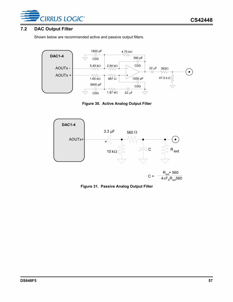
CS42448
7.2 DAC Output Filter
Shown below are recommended active and passive output filters.
AOUTx +
AOUTx - -
+
390 pF
C0G56222 F
4.75 k1800 pF
C0G
887
2.94 k5.49 k
1.65 k
1.87 k 22 F
1200 pF
C0G5600 pF
C0G
47.5 k
DAC1-4
Figure 30. Active Analog Output Filter
AOUTx+
3.3 µF
C
560
+
10 k R ext
Rext + 560C = 4FSRext 560
DAC1-4
Figure 31. Passive Analog Output Filter
DS648F5 57
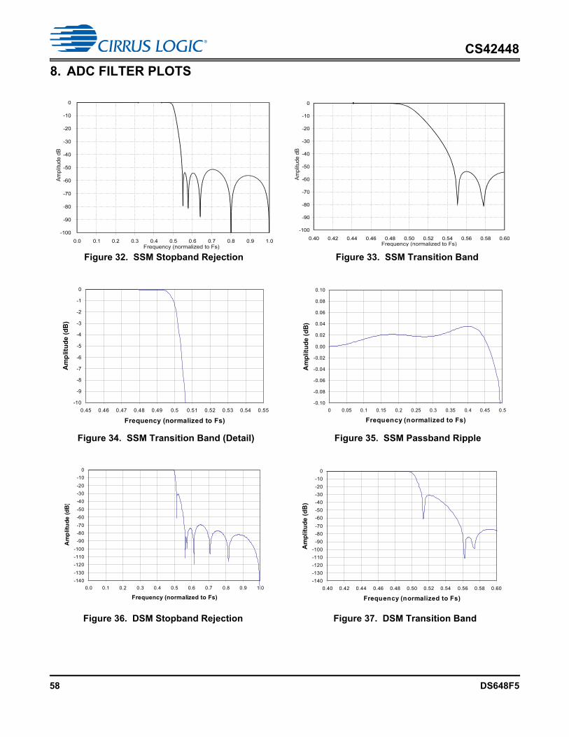
CS42448
8. ADC FILTER PLOTS
Figure 32. SSM Stopband Rejection Figure 33. SSM Transition Band
-10
-9
-8
-7
-6
-5
-4
-3
-2
-1
0
0.45 0.46 0.47 0.48 0.49 0.5 0.51 0.52 0.53 0.54 0.55
Frequency (normalized to Fs)
Am
plit
ud
e (d
B)
-0.10
-0.08
-0.06
-0.04
-0.02
0.00
0.02
0.04
0.06
0.08
0.10
0 0.05 0.1 0.15 0.2 0.25 0.3 0.35 0.4 0.45 0.5
Frequency (normalized to Fs)
Am
pli
tud
e (
dB
)
Figure 34. SSM Transition Band (Detail) Figure 35. SSM Passband Ripple
-140
-130
-120
-110
-100
-90
-80
-70
-60
-50
-40
-30
-20
-10
0
0.0 0.1 0.2 0.3 0.4 0.5 0.6 0.7 0.8 0.9 1.0
Frequency (normalized to Fs)
Am
plit
ud
e (
dB
)
-140
-130
-120
-110
-100
-90
-80
-70
-60
-50
-40
-30
-20
-10
0
0.40 0.42 0.44 0.46 0.48 0.50 0.52 0.54 0.56 0.58 0.60
Frequency (normalized to Fs)
Am
pli
tud
e (
dB
)
Figure 36. DSM Stopband Rejection Figure 37. DSM Transition Band
58 DS648F5

CS42448
‘
-0.10
-0 .08
-0 .06
-0 .04
-0 .02
0 .00
0 .02
0 .04
0 .06
0 .08
0.10
0.00 0.05 0 .10 0.15 0.20 0.25 0.30 0.35 0.40 0.45 0.50
Frequency (norm alized to Fs)
Am
plitu
de
(dB
)
-10
-9
-8
-7
-6
-5
-4
-3
-2
-1
0
0.46 0.47 0.48 0.49 0.50 0.51 0.52
Frequency (normalized to Fs)
Am
plit
ud
e (
dB
)
Figure 38. DSM Transition Band (Detail) Figure 39. DSM Passband Ripple
-140
-130-120
-110
-100
-90-80
-70
-60-50
-40
-30
-20-10
0
0.0 0.1 0.2 0.3 0.4 0.5 0 .6 0.7 0.8 0.9 1.0
Frequency (norm alized to Fs )
Am
plitu
de
(dB
)
-140
-130-120
-110
-100
-90-80
-70
-60-50
-40
-30
-20-10
0
0.20 0.25 0.30 0.35 0.40 0.45 0.50 0.55 0.60 0.65 0.70 0.75 0.80 0.85
Frequency (norm alized to Fs )
Am
plitu
de
(dB
)
Figure 40. QSM Stopband Rejection Figure 41. QSM Transition Band
-0 .10
-0.08
-0.06
-0.04
-0.02
0.0 0
0.0 2
0.0 4
0.0 6
0.0 8
0.10
0 .00 0.03 0 .05 0.08 0 .10 0.13 0.15 0.18 0.20 0.23 0.25 0.28Frequency (norm alized to Fs)
Am
plitu
de
(dB
)
Figure 42. QSM Transition Band (Detail) Figure 43. QSM Passband Ripple
-10
-9
-8
-7
-6
-5
-4
-3
-2
-1
0
0.10 0.15 0.20 0.25 0.30 0.35 0.40 0.45 0.50
Frequency (normalized to Fs)
Am
pli
tud
e (
dB
)
DS648F5 59

CS42448
9. DAC FILTER PLOTS
Figure 44. SSM Stopband Rejection Figure 45. SSM Transition Band
0 0.05 0.1 0.15 0.2 0.25 0.3 0.35 0.4 0.45 0.5
-0.25
-0. 2
-0.15
-0. 1
-0.05
0
0.05
Frequency (normalized to Fs)
Am
plitu
de d
B
Figure 46. SSM Transition Band (detail) Figure 47. SSM Passband Ripple
Figure 48. DSM Stopband Rejection Figure 49. DSM Transition Band
60 DS648F5
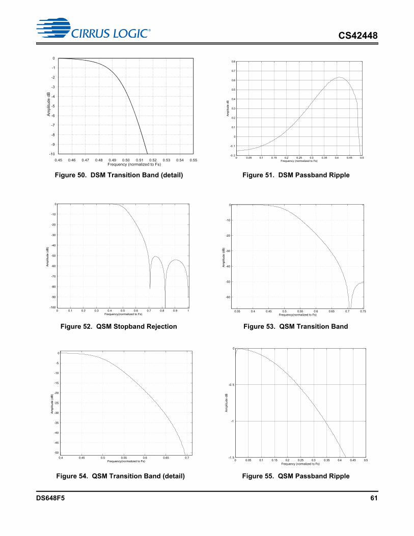
CS42448
0 0.05 0.1 0.15 0.2 0.25 0.3 0.35 0.4 0.45 0.5-0. 2
-0. 1
0
0.1
0.2
0.3
0.4
0.5
0.6
0.7
0.8
Frequency (normalized to Fs)
Am
plitu
de d
B
Figure 50. DSM Transition Band (detail) Figure 51. DSM Passband Ripple
0.35 0.4 0.45 0.5 0.55 0.6 0.65 0.7 0.75
-60
-50
-40
-30
-20
-10
0
Am
plitu
de (
dB)
Frequency(normalized to Fs)
Figure 52. QSM Stopband Rejection Figure 53. QSM Transition Band
0 0.1 0.2 0.3 0.4 0.5 0.6 0.7 0.8 0.9 1-100
-90
-80
-70
-60
-50
-40
-30
-20
-10
0
Am
plitu
de (
dB)
Frequency(normalized to Fs)
0.4 0.45 0.5 0.55 0.6 0.65 0.7
-50
-45
-40
-35
-30
-25
-20
-15
-10
-5
0
Am
plitu
de (
dB)
Frequency(normalized to Fs) 0 0.05 0.1 0.15 0.2 0.25 0.3 0.35 0.4 0.45 0.5-1. 5
-1
-0. 5
0
Frequency (normalized to Fs)
Am
plit
ud
e d
B
Figure 54. QSM Transition Band (detail) Figure 55. QSM Passband Ripple
DS648F5 61

CS42448
10.PARAMETER DEFINITIONS
Dynamic Range
The ratio of the rms value of the signal to the rms sum of all other spectral components over the specifiedbandwidth. Dynamic Range is a signal-to-noise ratio measurement over the specified band width made witha -60 dBFS signal. 60 dB is added to resulting measurement to refer the measurement to full-scale. Thistechnique ensures that the distortion components are below the noise level and do not affect the measure-ment. This measurement technique has been accepted by the Audio Engineering Society, AES17-1991,and the Electronic Industries Association of Japan, EIAJ CP-307. Expressed in decibels.
Total Harmonic Distortion + Noise
The ratio of the rms value of the signal to the rms sum of all other spectral components over the specifiedband width (typically 10 Hz to 20 kHz), including distortion components. Expressed in decibels. Measuredat -1 and -20 dBFS as suggested in AES17-1991 Annex A.
Frequency Response
A measure of the amplitude response variation from 10 Hz to 20 kHz relative to the amplitude response at1 kHz. Units in decibels.
Interchannel Isolation
A measure of crosstalk between the left and right channel pairs. Measured for each channel at the convert-er's output with no signal to the input under test and a full-scale signal applied to the other channel. Units indecibels.
Interchannel Gain Mismatch
The gain difference between left and right channel pairs. Units in decibels.
Gain Error
The deviation from the nominal full-scale analog output for a full-scale digital input.
Gain Drift
The change in gain value with temperature. Units in ppm/°C.
Offset Error
The deviation of the mid-scale transition (111...111 to 000...000) from the ideal. Units in mV.
62 DS648F5

CS42448
11.REFERENCES1. Cirrus Logic, AN18: Layout and Design Rules for Data Converters and Other Mixed Signal Devices,
Version 6.0, February 1998.
2. Cirrus Logic, Techniques to Measure and Maximize the Performance of a 120 dB, 96 kHz A/D ConverterIntegrated Circuit, by Steven Harris, Steven Green and Ka Leung. Presented at the 103rd Convention of theAudio Engineering Society, September 1997.
3. Cirrus Logic, A Stereo 16-bit Delta-Sigma A/D Converter for Digital Audio, by D.R. Welland, B.P. Del Signo-re, E.J. Swanson, T. Tanaka, K. Hamashita, S. Hara, K. Takasuka. Paper presented at the 85th Conventionof the Audio Engineering Society, November 1988.
4. Cirrus Logic, The Effects of Sampling Clock Jitter on Nyquist Sampling Analog-to-Digital Converters, andon Oversampling Delta Sigma ADC's, by Steven Harris. Paper presented at the 87th Convention of the Au-dio Engineering Society, October 1989.
5. Cirrus Logic, An 18-Bit Dual-Channel Oversampling Delta-Sigma A/D Converter, with 19-Bit Mono Applica-tion Example, by Clif Sanchez. Paper presented at the 87th Convention of the Audio Engineering Society,October 1989.
6. Cirrus Logic, How to Achieve Optimum Performance from Delta-Sigma A/D and D/A Converters, by StevenHarris. Presented at the 93rd Convention of the Audio Engineering Society, October 1992.
7. Cirrus Logic, A Fifth-Order Delta-Sigma Modulator with 110 dB Audio Dynamic Range, by I. Fujimori, K.Hamashita and E.J. Swanson. Paper presented at the 93rd Convention of the Audio Engineering Society,October 1992.
8. Philips Semiconductor, The I²C-Bus Specification: Version 2.1, January 2000. http://www.semiconductors.philips.com
DS648F5 63

CS42448
12.PACKAGE INFORMATION
12.1 Thermal Characteristics
INCHES MILLIMETERS
DIM MIN NOM MAX MIN NOM MAX
A --- 0.55 0.063 --- 1.40 1.60
A1 0.002 0.004 0.006 0.05 0.10 0.15
B 0.007 0.008 0.011 0.17 0.20 0.27
D 0.461 0.472 BSC 0.484 11.70 12.0 BSC 12.30
D1 0.390 0.393 BSC 0.398 9.90 10.0 BSC 10.10
E 0.461 0.472 BSC 0.484 11.70 12.0 BSC 12.30
E1 0.390 0.393 BSC 0.398 9.90 10.0 BSC 10.10
e* 0.016 0.020 BSC 0.024 0.40 0.50 BSC 0.60
L 0.018 0.024 0.030 0.45 0.60 0.75
0.000° 4° 7.000° 0.00° 4° 7.00°* Nominal pin pitch is 0.50 mmControlling dimension is mm.JEDEC Designation: MS026
Parameter Symbol Min Typ Max Units
Junction to Ambient Thermal Impedance 2 Layer Board4 Layer Board
JAJA
--
5037
--
°C/Watt°C/Watt
64L LQFP PACKAGE DRAWING
E1E
D1D
1
e
L
B
A1
A
64 DS648F5

CS42448
13.ORDERING INFORMATION
14.REVISION HISTORY
Product Description Package Pb-Free Grade Temp Range Container Order #
CS424486-in, 8-out CODEC forSurround Sound Apps
64L-LQFP YESCommercial -10° to +70° C
Rail CS42448-CQZ Tape & Reel CS42448-CQZR
Automotive -40° to +105° CRail CS42448-DQZ
Tape & Reel CS42448-DQZR CDB42448 CS42448 evaluation board - - - - - CDB42448
Revision Changes
F1Updated temperature and voltage specifications in the “Recommended Operating Conditions” on page 10. Added test conditions to the Analog Input and Analog Output Characteristics tables.
F2Corrected polarities for pin numbers 31, 32, 38, 39 in the “Typical Connection Diagram” on page 9 and cor-rected the number designations for the AOUT7+ and AOUT7- pins in the Pin Descriptions table on page 6.
F3Updated input impedance specification for Differential and Single-Ended Inputs in “Analog Input Characteris-tics (Commercial)” on page 11 and “Analog Input Characteristics (Automotive)” on page 12.
F4
• Updated Note 12 regarding triangular PDF dither in “Analog Output Characteristics (Automotive)” on page 15.
• Added rows for “High-Level Output Voltage at Io=100 A” and “Low-Level Output Voltage at Io=100 A” in “Digital Interface Specifications & Characteristics” on page 24.
• Updated MFreq2:0 == 001 and MFreq2:0 == 011 (ratios of 384x and 768x) to "Reserved" in Table 10 and Table 11. Removed references to these ratios and their divisors in Table 2 through Table 8.
F5Updates to clarify the behavior of the ADC Overflow bit; full-scale signal with single-ended input. • Explanatory text preceding Figure 10 on page 26. • Explanatory text, “ADC Overflow (ADCX_OVFL)” on page 52.
DS648F5 65

CS42448
Contacting Cirrus Logic SupportFor all product questions and inquiries, contact a Cirrus Logic Sales Representative. To find the one nearest you, go to www.cirrus.com.
IMPORTANT NOTICE
The products and services of Cirrus Logic International (UK) Limited; Cirrus Logic, Inc.; and other companies in the Cirrus Logic group (collectively either “Cirrus Logic” or “Cirrus”) are sold subject to Cirrus Logic’s terms and conditions of sale supplied at the time of order acknowledgment, including those pertaining to warranty, indemnification, and limitation of liability. Software is provided pursuant to applicable license terms. Cirrus Logic reserves the right to make changes to its products and specifications or to discontinue any product or service without notice. Customers should therefore obtain the latest version of relevant information from Cirrus Logic to verify that the information is current and complete. Testing and other quality control techniques are utilized to the extent Cirrus Logic deems necessary. Specific testing of all parameters of each device is not necessarily performed. In order to minimize risks associated with customer applications, the customer must use adequate design and operating safeguards to minimize inherent or procedural hazards. Cirrus Logic is not liable for applications assistance or customer product design. The customer is solely responsible for its selection and use of Cirrus Logic products. Use of Cirrus Logic products may entail a choice between many different modes of operation, some or all of which may require action by the user, and some or all of which may be optional. Nothing in these materials should be interpreted as instructions or suggestions to choose one mode over another. Likewise, description of a single mode should not be interpreted as a suggestion that other modes should not be used or that they would not be suitable for operation. Features and operations described herein are for illustrative purposes only.
CERTAIN APPLICATIONS USING SEMICONDUCTOR PRODUCTS MAY INVOLVE POTENTIAL RISKS OF DEATH, PERSONAL INJURY, OR SEVERE PROPERTY OR ENVIRONMENTAL DAMAGE (“CRITICAL APPLICATIONS”). CIRRUS LOGIC PRODUCTS ARE NOT DESIGNED, AUTHORIZED OR WARRANTED FOR USE IN PRODUCTS SURGICALLY IMPLANTED INTO THE BODY, AUTOMOTIVE SAFETY OR SECURITY DEVICES, NUCLEAR SYSTEMS, LIFE SUPPORT PRODUCTS OR OTHER CRITICAL APPLICATIONS. INCLUSION OF CIRRUS LOGIC PRODUCTS IN SUCH APPLICATIONS IS UNDERSTOOD TO BE FULLY AT THE CUSTOMER’S RISK AND CIRRUS LOGIC DISCLAIMS AND MAKES NO WARRANTY, EXPRESS, STATUTORY OR IMPLIED, INCLUDING THE IMPLIED WARRANTIES OF MERCHANTABILITY AND FITNESS FOR PARTICULAR PURPOSE, WITH REGARD TO ANY CIRRUS LOGIC PRODUCT THAT IS USED IN SUCH A MANNER. IF THE CUSTOMER OR CUSTOMER’S CUSTOMER USES OR PERMITS THE USE OF CIRRUS LOGIC PRODUCTS IN CRITICAL APPLICATIONS, CUSTOMER AGREES, BY SUCH USE, TO FULLY INDEMNIFY CIRRUS LOGIC, ITS OFFICERS, DIRECTORS, EMPLOYEES, DISTRIBUTORS AND OTHER AGENTS FROM ANY AND ALL LIABILITY, INCLUDING ATTORNEYS’ FEES AND COSTS, THAT MAY RESULT FROM OR ARISE IN CONNECTION WITH THESE USES.
This document is the property of Cirrus Logic and by furnishing this information, Cirrus Logic grants no license, express or implied, under any patents, mask work rights, copyrights, trademarks, trade secrets or other intellectual property rights. Any provision or publication of any third party’s products or services does not constitute Cirrus Logic’s approval, license, warranty or endorsement thereof. Cirrus Logic gives consent for copies to be made of the information contained herein only for use within your organization with respect to Cirrus Logic integrated circuits or other products of Cirrus Logic, and only if the reproduction is without alteration and is accompanied by all associated copyright, proprietary and other notices and conditions (including this notice). This consent does not extend to other copying such as copying for general distribution, advertising or promotional purposes, or for creating any work for resale. This document and its information is provided “AS IS” without warranty of any kind (express or implied). All statutory warranties and conditions are excluded to the fullest extent possible. No responsibility is assumed by Cirrus Logic for the use of information herein, including use of this information as the basis for manufacture or sale of any items, or for infringement of patents or other rights of third parties. Cirrus Logic, Cirrus, the Cirrus Logic logo design, and SoundClear are among the trademarks of Cirrus Logic. Other brand and product names may be trademarks or service marks of their respective owners.
Copyright © 2013–2017 Cirrus Logic, Inc. All rights reserved.
SPI is a trademark of Motorola.
66 DS648F5