Embed Size (px)
Citation preview
CS1180 Specification
Copyright Reserved Shenzhen Chipsea Technologies CO., LTD. 1 -26
www.chipsea.com
CCSS11118800 SSppeecciiffiiccaattiioonn VV11..00
Feb.2009
CS1180 Specification
Copyright Reserved Shenzhen Chipsea Technologies CO., LTD. 2 -26
www.chipsea.com
CCoonntteennttss 1 CS1180 DESCRIPTION ............................................................................................................... 4
1.1 CS1180 FEATURES ................................................................................................................. 4 1.2 APPLICATIONS ...................................................................................................................... 4 1.3 FUNCTION DESCRIPTION .................................................................................................... 5
2 CS1180 CHARACTERISTIC DESCRIPTION .......................................................................... 6
2.1 ABSOLUTE MAXIMUM RATINGS ...................................................................................... 6 2.2 DIGITAL CHARACTERISTICS ............................................................................................. 6 2.3 PINS and PACKAGING ........................................................................................................... 7 2.4 ELECTRICAL CHARACTERISTICS ..................................................................................... 9 2.5 TIMING CHARACTERISTICS ............................................................................................. 11
3 CS1180 FUNCTION MODULE DESCRIPTION .................................................................... 13
3.1. ANALOG INPUT BUFFER ................................................................................................... 13 3.2. PROGRAMMABLE GAIN AMPLIFIER (PGA) .................................................................. 13 3.3. MODULATOR ....................................................................................................................... 13 3.4. CALIBRATION ...................................................................................................................... 13
3.3.1 SYSTEM CALIBRATION ............................................................................................... 13 3.4 EXTERNAL VOLTAGE REFERENCE ................................................................................ 14 3.5 CLOCK UNIT......................................................................................................................... 14 3.6 DIGITAL FILTER (FIR) ........................................................................................................ 14 3.7 SERIAL PERIPHERAL INTERFACE (SPI) ......................................................................... 15
3.7.1 CHIP SELECT (CS) ......................................................................................................... 15 3.7.2 SERIAL CLOCK (SCLK) ................................................................................................ 15 3.7.3 DATA INPUT (SDI) and DATA OUTPUT (SDO) .......................................................... 15 3.7.4 DATA READY (DRDY) .................................................................................................. 15
3.8 POWER-UP RESET and CHIP RESET ................................................................................. 15
4 CS1180 REGISTER DESCRIPTION ........................................................................................ 16
4.1 RIGISTER LIST ..................................................................................................................... 16 4.2 DETAILED REGISTER DEFINITIONS ............................................................................... 17
5 CS1180 COMMAND DESCRIPTION ...................................................................................... 21
5.1 CS1180 COMMAND LIST .................................................................................................... 21 5.2 DETAILED COMMANDS DESCRIPTION .......................................................................... 22
6 CS1180 PACKAGE ..................................................................................................................... 25

CS1180 Specification
Copyright Reserved Shenzhen Chipsea Technologies CO., LTD. 3 -26
www.chipsea.com
Diagram Lists Figure 1 CS1180 Principle Block Diagram ..................................................................................... 5Figure 2 Pin Diagram ...................................................................................................................... 7Figure 3 Timing Diagram ............................................................................................................. 11Figure 4 Schematic of Using External Crystal ............................................................................. 14
Table Lists
Table 1 Limit Value ............................................................................................................................ 6Table 2 Digital Characteristics ........................................................................................................... 6Table 3 Pin Description ...................................................................................................................... 7Table 4 Package .................................................................................................................................. 8Table 5 Electrical Characteristics (AVDD=5V) ................................................................................. 9Table 6 Electrical Characteristics (AVDD=3V) ............................................................................... 10Table 7 Timing Table ....................................................................................................................... 12Table 8 The Sample Frequency of The Modulator ........................................................................... 13Table 9 The Relation Between External Reference Voltage and RAN ............................................ 14Table 10 Registers List ................................................................................................................... 16Table 11 Commands Table ............................................................................................................. 21

CS1180 Specification
Copyright Reserved Shenzhen Chipsea Technologies CO., LTD. 4 -26
www.chipsea.com
1 CS1180 DESCRIPTION
The CS1180 is precision, low power dissipation, Analog-to-Digital (A/D) converter with 24-bit resolution and up to 19-bit ENOB. The CS1180 has world wide applications in industrial process control, weigh scales, liquid/gas chemical analysis, blood analysis, smart transmitters and portable instrumentation.
1.1 CS1180 FEATURES 24 bits no missing code, 19 bits effective precision analog-to-digital converter Simultaneous 50Hz and 60Hz rejection (reaching -90dB) 0.0030% INL PGA gains from 1 to 128 Single-cycle setting Programmable ADC data output rates External differential reference of 0.1V to 5V On-chip calibration Integrated compatible SPI bus interface
1.2 APPLICATIONS Industrial process control Weight scales Liquid/gas chemical analysis Blood analysis Smart transmitters Portable instrumentation
CS1180 Specification
Copyright Reserved Shenzhen Chipsea Technologies CO., LTD. 5 -26
www.chipsea.com
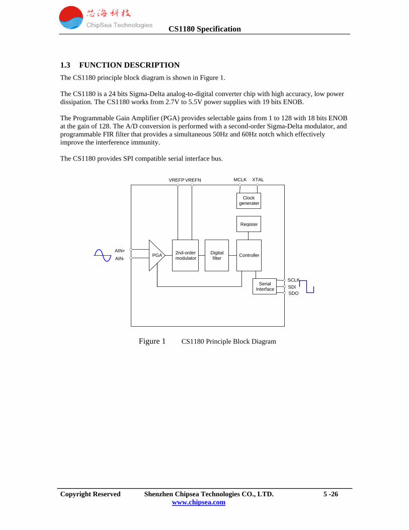
1.3 FUNCTION DESCRIPTION The CS1180 principle block diagram is shown in Figure 1. The CS1180 is a 24 bits Sigma-Delta analog-to-digital converter chip with high accuracy, low power dissipation. The CS1180 works from 2.7V to 5.5V power supplies with 19 bits ENOB. The Programmable Gain Amplifier (PGA) provides selectable gains from 1 to 128 with 18 bits ENOB at the gain of 128. The A/D conversion is performed with a second-order Sigma-Delta modulator, and programmable FIR filter that provides a simultaneous 50Hz and 60Hz notch which effectively improve the interference immunity. The CS1180 provides SPI compatible serial interface bus.
Figure 1 CS1180 Principle Block Diagram
PGA 2 nd - order modulator
Digital filter Controller
Register
Serial Interface
Clock generater
VREFP VREFN
SCLK
MCLK XTAL
AIN + AIN -
SDI SDO
CS1180 Specification
Copyright Reserved Shenzhen Chipsea Technologies CO., LTD. 6 -26
www.chipsea.com
2 CS1180 CHARACTERISTIC DESCRIPTION
2.1 ABSOLUTE MAXIMUM RATINGS Table 1 shows the limit values of the CS1180
Table 1 Limit Value DESCRIPTION SYMBOL MIN MAX UNITS AVDD to AGND AVDD -0.3 6 V DVDD to DGND DVDD -0.3 6 V DGND to AGND DVGND -0.3 0.3 V
Transient Input Current 100 mA Continuous Input Current 10 mA
Digital Input Voltage to DGND -0.3 DVDD+0.3 V Digital Output Voltage to DGND -0.3 DVDD+0.3 V
Max. Junction Temperature 150 oC Operating Temperature -40 85 oC Storage Temperature -60 150 oC
Lead Temperature (Soldering, 10s) 240 oC
2.2 DIGITAL CHARACTERISTICS Table 2 shows the digital characteristics of the CS1180
Table 2 Digital Characteristics PARAMETER MIN TYP MAX UNITS CONDITION
VIH 0.8×DVDD DVDD V VIL DGND 0.2×DVDD V VOH DVDD-0.4 DVDD+0.4 V Ioh=1mA VOL DGND DGND+0.4 V IoL=1mA IIH 10 uA VI=DVDD IIL -10 uA VI=DGND fosc 1 5 MHz tosc 200 1000 ns NOTES:The digital interface is CMOS logic.
CS1180 Specification
Copyright Reserved Shenzhen Chipsea Technologies CO., LTD. 7 -26
www.chipsea.com
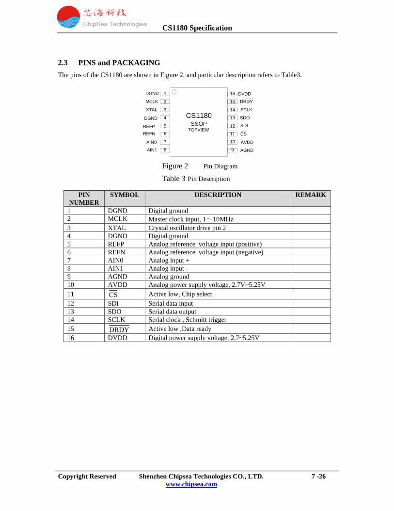
2.3 PINS and PACKAGING The pins of the CS1180 are shown in Figure 2, and particular description refers to Table3.
Figure 2 Pin Diagram
Table 3 Pin Description
PIN NUMBER
SYMBOL DESCRIPTION REMARK
1 DGND Digital ground 2 MCLK Master clock input, 1~10MHz 3 XTAL Crystal oscillator drive pin 2 4 DGND Digital ground 5 REFP Analog reference voltage input (positive) 6 REFN Analog reference voltage input (negative) 7 AIN0 Analog input + 8 AIN1 Analog input - 9 AGND Analog ground 10 AVDD Analog power supply voltage, 2.7V~5.25V 11 CS Active low, Chip select 12 SDI Serial data input 13 SDO Serial data output 14 SCLK Serial clock , Schmitt trigger 15 DRDY Active low ,Data ready 16 DVDD Digital power supply voltage, 2.7~5.25V
CS 1180 SSOP
TOPVIEW
1 2 3 4 5 6 7 8
16 15 14 13 12 11 10 9
DGND MCLK XTAL
DGND REFP REFN
AIN 0 AIN 1 AGND
AVDD CS SDI SDO SCLK DRDY
DVDD
CS1180 Specification
Copyright Reserved Shenzhen Chipsea Technologies CO., LTD. 8 -26
www.chipsea.com
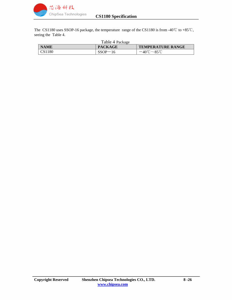
The CS1180 uses SSOP-16 package, the temperature range of the CS1180 is from -40℃ to +85℃, seeing the Table 4.
Table 4 Package NAME PACKAGE TEMPERATURE RANGE CS1180 SSOP-16 -40℃~85℃
CS1180 Specification
Copyright Reserved Shenzhen Chipsea Technologies CO., LTD. 9 -26
www.chipsea.com
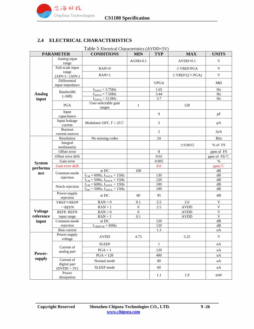
2.4 ELECTRICAL CHARACTERISTICS Table 5 Electrical Characteristics (AVDD=5V)
PARAMETER CONDITIONS MIN TYP MAX UNITS
Analog input
Analog input range AGND-0.1 AVDD+0.1 V
Full-scale input range
(AIN+) - (AIN-)
RAN=0 ±VREF/PGA V
RAN=1 ±VREF/(2×PGA) V Differential
input impedance 5/PGA MΩ
Bandwidth (-3dB)
fDATA = 3.75Hz 1.65 Hz fDATA = 7.50Hz 3.44 Hz fDATA = 15.0Hz 3.7 Hz
PGA User-selectable gain ranges 1 128
Input capacitance 9 pF
Input leakage current Modulator OFF, T = 25℃ 5 pA
Burnout current sources 2 2uA
System performa
nce
Resolution No missing codes 24 Bits Integral
nonlinearity ±0.0015 % of FS
Offset error 8 ppm of FS Offset error drift 0.02 ppm of FS/℃
Gain error 0.005 % Gain error drift 8.0 ppm/℃
Common-mode rejection
at DC 100 dB fCM = 60Hz, fDATA = 15Hz 130 dB fCM = 50Hz, fDATA = 15Hz 120 dB
Notch rejection fCM = 60Hz, fDATA = 15Hz 100 dB fSIG = 50Hz, fDATA = 15Hz 100 dB
Power-supply rejection at DC 80 95 dB
Voltage reference
input
VREF≡REFP-REFN
RAN = 0 0.1 2.5 2.6 V RAN = 1 0 2.5 AVDD V
REFP, REFN input range
RAN = 0 0 AVDD V RAN = 1 0.1 AVDD V
Common-mode rejection
at DC 120 dB fVREFCM = 60Hz 120 dB
Bias current 1.3 uA
Power-supply
Power-supply voltage AVDD 4.75 5.25 V
Current of analog part
SLEEP 1 nA PGA = 1 120 uA
PGA = 128 400 uA Current of digital part
(DVDD = 3V)
Normal mode 80 uA
SLEEP mode 60 uA Power
dissipation 1.1 1.9 mW

CS1180 Specification
Copyright Reserved Shenzhen Chipsea Technologies CO., LTD. 10 -26
www.chipsea.com
Table 6 Electrical Characteristics (AVDD=3V) PARAMETER CONDITION MIN TYP MAX UNITS
Analog input
Analog input range AGND-0.1 AVDD+0.1 V
Full-scale input range
(AIN+) - (AIN-)
RAN=0 ±VREF/PGA V
RAN=1 ±VREF/(2×PGA) V
Differential input impedance 5/PGA MΩ
Bandwidth (-3dB)
fDATA = 3.75Hz 1.65 Hz fDATA = 7.50Hz 3.44 Hz fDATA = 15.0Hz 14.6 Hz
PGA User-selectable gain ranges 1 128
Input capacitance 9 pF
Input leakage current Modulator OFF, T = 25℃ 5 pA
Burnout current sources 2 2uA
System performa
nce
Resolution No missing codes 24 Bits Integral
nonlinearity ±0.0015 % of FS
Offset error 15 ppm of FS Offset error drift 0.04 ppm of FS/℃
Gain error 0.01 % Gain error drift 8.0 ppm/℃
Common-mode rejection
at DC 100 dB fCM = 60Hz, fDATA = 15Hz 130 dB fCM = 50Hz, fDATA = 15Hz 120 dB
Notch rejection fCM = 60Hz, fDATA = 15Hz 100 dB fSIG = 50Hz, fDATA = 15Hz 100 dB
Power-supply rejection at DC 75 90 dB
Voltage reference
input
VREF≡REFP-REFN
RAN = 0 0.1 1.25 1.30 V RAN = 1 0 2.5 2.6 V
REFP, REFN input range
RAN = 0 0 AVDD V RAN = 1 0.1 AVDD V
Common-mode rejection
at DC 120 dB fVREFCM = 60Hz 120 dB
Bias current 0.65 uA
Power-supply
Power-supply voltage AVDD 2.7 3.3 V
Current of analog part
SLEEP 1 nA PGA = 1 107 uA
PGA = 128 360 uA Current of digital part
(DVDD = 3V)
Normal mode 50 uA
SLEEP mode 40 uA
Power dissipation 0.6 1.2 mW
CS1180 Specification
Copyright Reserved Shenzhen Chipsea Technologies CO., LTD. 11 -26
www.chipsea.com
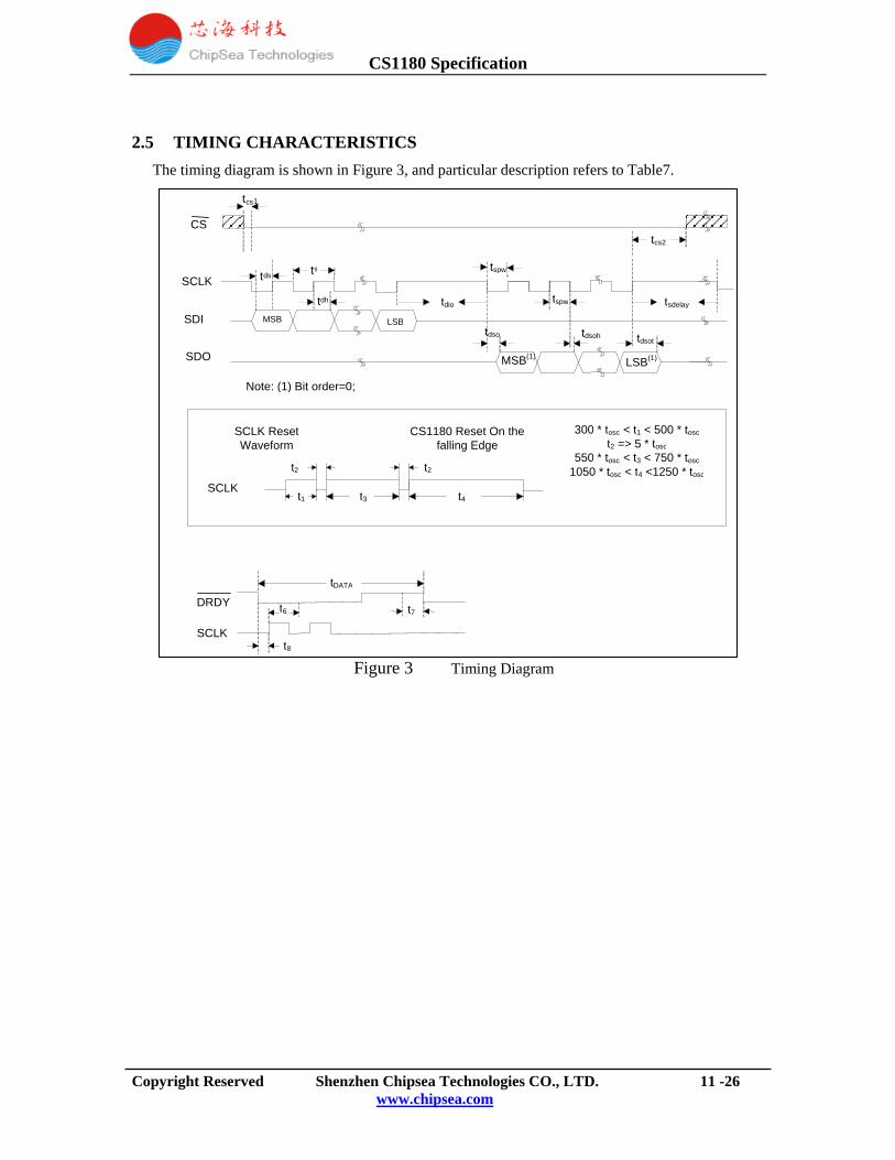
2.5 TIMING CHARACTERISTICS The timing diagram is shown in Figure 3, and particular description refers to Table7.
Figure 3 Timing Diagram
t
SCLK
SDI
SDO
t t
MSB LSB
MSB ( 1 )
t spw
t dso t dsoh
t cs 2
t dsot
t sdelay t dio
LSB ( 1 )
Note : ( 1 ) Bit order = 0 ;
t 1
t 2
t 3
t 2
t 4 SCLK
SCLK Reset Waveform
CS 1180 Reset On the falling Edge
t 8
t DATA t 6 t 7
300 * t osc < t 1 < 500 * t osc t 2 = > 5 * t osc
550 * t osc < t 3 < 750 * t osc 1050 * t osc < t 4 < 1250 * t osc
SCLK
s t
cs 1
t spw
ds dh
CS
DRDY
CS1180 Specification
Copyright Reserved Shenzhen Chipsea Technologies CO., LTD. 12 -26
www.chipsea.com
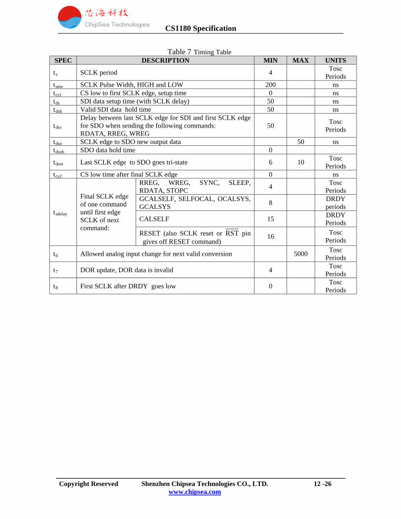
Table 7 Timing Table SPEC DESCRIPTION MIN MAX UNITS
t SCLK period s 4 Tosc Periods
t SCLK Pulse Width, HIGH and LOW spw 200 ns t CS low to first SCLK edge, setup time cs1 0 ns t SDI data setup time (with SCLK delay) ds 50 ns t Valid SDI data hold time dsh 50 ns
tDelay between last SCLK edge for SDI and first SCLK edge for SDO when sending the following commands: dio RDATA, RREG, WREG
50 Tosc Periods
t SCLK edge to SDO new output data dso 50 ns t SDO data hold time dsoh 0
t Last SCLK edge to SDO goes tri-state dsot 6 10 Tosc Periods
t CS low time after final SCLK edge cs2 0 ns
t
Final SCLK edge of one command until first edge SCLK of next command:
sdelay
RREG, WREG, SYNC, SLEEP, RDATA, STOPC 4 Tosc
Periods GCALSELF, SELFOCAL, OCALSYS, GCALSYS 8 DRDY
periods
CALSELF 15 DRDY Periods
RESET (also SCLK reset or RST pin gives off RESET command)
16 Tosc Periods
t Allowed analog input change for next valid conversion 6 5000 Tosc Periods
t DOR update, DOR data is invalid 7 4 Tosc Periods
t First SCLK after DRDY goes low 8 0 Tosc Periods
CS1180 Specification
Copyright Reserved Shenzhen Chipsea Technologies CO., LTD. 13 -26
www.chipsea.com
3 CS1180 FUNCTION MODULE DESCRIPTION
3.1. ANALOG INPUT BUFFER The input impedance of the CS1180 is about 5MΩ/PGA with the buffer off, but the input impedance is up to about 5GΩ with the buffer on. The buffer can be controlled by the BUF pin and the register ACR. When the BUF bit in ACR register and BUF pin is high, the buffer is on. The buffer will draw additional power dissipation when activated. The power depends on the PGA setting. When PGA=1, the buffer produces approximately 50uA additional current; When the PGA=128, the buffer produces approximately 150uA additional current. The input range should be AGND+0.3V to AVDD-1.5V with the buffer on.
3.2. PROGRAMMABLE GAIN AMPLIFIER (PGA) The Programmable Gain Amplifier (PGA) can be set to 1, 2, 4, 8, 16, 32, 64, or 128. Using PGA can improve the ENOB of the A/D converter. For example, when PGA=1, the full scale input is 5V, the converter can resolve down to 4.7uV; when PGA=128, the full scale input is 39mV, the converter can resolve down to 75nV.
3.3. MODULATOR The Modulator of the CS1180 is a single loop, second order Sigma-Delta system. The sample frequency of the modulator is controlled by the SPEED bit in ACR register (ACR bit 5). The sample frequency is shown in Table8:
Table 8 The Sample Frequency of The Modulator
Frequency(MHz) SPEED
ADC Sample Frequency
(KHz)
Data Output Rate (Hz) Notch Frequency
(Hz) DR = 00 DR = 01 DR = 10
2.4576 0 19.200 15 7.5 3.75 50/60 1 9.600 7.5 3.75 1.875 25/30
4.9152 0 38.400 30 15 7.5 100/120 1 19.200 15 7.5 3.75 50/60
3.4. CALIBRATION The CS1180 provides both self calibration and system calibration which include offset and gain calibration of the A/D converter. During calibration, the DRDY signal will be held at high, which indicate the result of the AD converter is invalid. In order to ensure the accuracy of the A/D converter, the calibration should be performed after power-up, a change in temperature, or a change of the PGA. At the completion of the calibration, the DRDY signal goes low, indicating the calibration is finished. The first output data of the converter after calibration is invalid because of the delay of the inside circuit, and the second output data is valid.
3.3.1 SYSTEM CALIBRATION
System calibration corrects the offset and gain errors of the chip and the system. When performing system calibration, appropriate signal must be applied to the inputs. The commands of system

CS1180 Specification
Copyright Reserved Shenzhen Chipsea Technologies CO., LTD. 14 -26
www.chipsea.com
calibration include OCALSYS and GCALSYS. The command OCALSYS corrects the offset error; the command GCALSYS corrects the gain error. Each calibration is finished in eight TDATA cycles. The differential input voltage must be zero for offset calibration. The CS1180 computes the offset error for eliminating the system offset error. The input voltage must be positive full-scale for gain calibration. The CS1180 computes the gain error
for eliminating the system gain error.
3.4 EXTERNAL VOLTAGE REFERENCE The CS1180 requires an external reference voltage which connects to REFP and REFN pins. ACR register decides the specific reference voltage value. The value can’t exceed the supply voltage. The specific voltage value is shown in Table9:
Table 9 The Relation Between External Reference Voltage and RAN RAN (ACR.2) Power Voltage (V) Reference Voltage (V) Remark
0 5 <=2.5 1 5 <=5 0 3.0 <=1.25 1 3.0 <=2.5
3.5 CLOCK UNIT The clock source for the CS1180 can be provided from external clock, a crystal, or oscillator. If the clock source is external clock, the clock is only connected to MCLK pin, and the XTAL pin is unused. If the source is a crystal, the clock circuit is shown in Figure5: (two capacitances of 10~20pF connect to the MCLK and XTAL pins)
Figure 4 Schematic of Using External Crystal
3.6 DIGITAL FILTER (FIR) The CS1180 has a programmable FIR filter which can be set to different data output rates. When the clock is 2.4576MHz, the data output rate can be set to 15Hz, 7.5Hz, or 3.75Hz. Under these conditions, the FIR filter rejects both 50Hz and 60Hz interference. Using other clock frequency can get other data output rates, and the notch frequencies change simultaneously. For example, when the clock frequency is 3.6864MHZ, the register is under the default setting, and the data output rate is:
(3.6864MHz/2.4576MHz) ×15Hz = 22.5Hz Notch frequency:
( 3.6864MHz/2.4576MHz ) ×( 50Hz and 60Hz ) = ( 75Hz and 90Hz )
C2 C1
MCLK
XTAL
CS1180 Specification
Copyright Reserved Shenzhen Chipsea Technologies CO., LTD. 15 -26
www.chipsea.com
3.7 SERIAL PERIPHERAL INTERFACE (SPI) The CS1180 can communicate with external controller through the SPI bus. The CS1180 only operates in slave mode. The serial interface is a standard four-wire SPI interface, including CS, SCLK, SDI, and SDO.
3.7.1 CHIP SELECT (CS)
Before communicating with the CS1180, the external controller must send the chip select (CS) signal to the chip. During the communication, the CS signal must be maintained at low. When the CS signal is high, the entire SPI is reset. CS can be hard-wired low, the SPI bus can work in the three-wire mode which fits for communicating with external controller.
3.7.2 SERIAL CLOCK (SCLK)
The serial clock features a Schmitt-triggered input, which is used for sampling the SDI and SDO signals. The SCLK must be very clean to prevent the sample error. If the SCLK doesn’t appear in three DRDY cycles, the SPI bus is reset on next SCLK and starts a new communication cycle. A special waveform can reset the entire chip. See the RESET chapter for more information.
3.7.3 DATA INPUT (SDI) and DATA OUTPUT (SDO)
The data input pin (SDI) and the data output pin (SDO) receive and send the data. The SDO is high impendence when unused, allowing SDI and SDO to be connected together and driven by a bidirectional bus.
3.7.4 DATA READY (DRDY)
The DRDY signal is used for indicating the status of the internal data registers. When the new data in the data output register (DOR) is ready, the DRDY signal goes low. After a read operation, the DRDY signal goes high. When the DOR register is ready to update, the DRDY goes high, which indicates the data in DOR is can’t be read. The status of DRDY also can be got from the seventh bit of ACR register.
3.8 POWER-UP RESET and CHIP RESET After power-up, the CS1180 is reset automatically. When the CS1180 is working normally, there
are two methods to reset the CS1180: sending RESET command, or sending specific waveform on the SCLK (the SCLK RESET waveform, as shown in the Timing Diagram of the CS1180).
CS1180 Specification
Copyright Reserved Shenzhen Chipsea Technologies CO., LTD. 16 -26
www.chipsea.com
4 CS1180 REGISTER DESCRIPTION
The CS1180 configures the working mode through a series of control registers, which are used for controlling data format, MUX setting, data rate, calibration, etc.
4.1 RIGISTER LIST Registers list is shown in Table 10:
Table 10 Registers List
Address(H) Register BIT 7 BIT 6 BIT 5 BIT 4 BIT 3 BIT 2 BIT 1 BIT 0
00 SETUP ID3 ID2 ID1 ID0 Reserved PGA2 PGA1 PGA0
01 MUX 0 0 0 0 0 0 0 1
02 ACR DRDY BU/ SPEED BUF BITOR RAN DR1 DR0
03 ODAC Reserved CHSEL ISET1 ISET0 Reserved Reserved Reserved Reserved
04 Reserved
05 Reserved
06 Reserved
07 OCC0 OCC07 OCC06 OCC05 OCC04 OCC03 OCC02 OCC01 OCC00
08 OCC1 OCC15 OCC14 OCC13 OCC12 OCC11 OCC10 OCC09 OCC08
09 OCC2 OCC23 OCC22 OCC21 OCC20 OCC19 OCC18 OCC17 OCC16
0A GCC0 GCC07 GCC06 GCC05 GCC04 GCC03 GCC02 GCC01 GCC00
0B GCC1 GCC15 GCC14 GCC13 GCC12 GCC11 GCC10 GCC09 GCC08
0C GCC2 GCC23 GCC22 GCC21 GCC20 GCC19 GCC18 GCC17 GCC16
0D DOR2 DOR23 DOR22 DOR21 DOR20 DOR19 DOR18 DOR17 DOR16
0E DOR1 DOR15 DOR14 DOR13 DOR12 DOR11 DOR10 DOR09 DOR08
0F DOR0 DOR07 DOR06 DOR05 DOR04 DOR03 DOR02 DOR01 DOR00
CS1180 Specification
Copyright Reserved Shenzhen Chipsea Technologies CO., LTD. 17 -26
www.chipsea.com
4.2 DETAILED REGISTER DEFINITIONS SETUP Register (Address = 00H, Reset Value = xxxx0000) PGA Control MSB LSB Bit 7 Bit 6 Bit 5 Bit 4 Bit 3 Bit 2 Bit 1 Bit 0 ID3 ID2 ID1 ID0 Reserved PGA2 PGA1 PGA0
SETUP. 7-4 : Code of the chip, factory programmed bits SETUP.3 : Reserved SETU.2-0 : PGA2/PGA1/PGA0, Programmable Gain Amplifier Gain Selection 000=1 (Default) 001=2 010=4 011=8 100=16 101=32 110=64 111=128
MUX Register (Address = 01H, Reset Value = 00000001) MSB LSB Bit 7 Bit 6 Bit 5 Bit 4 Bit 3 Bit 2 Bit 1 Bit 0
0 0 0 0 0 0 0 1 When the value of MUX register is 00H, the input of ADC is shorted inside, and the output of the ADC is the NOISE of ADC. The register must be 01H in the normal use.
CS1180 Specification
Copyright Reserved Shenzhen Chipsea Technologies CO., LTD. 18 -26
www.chipsea.com
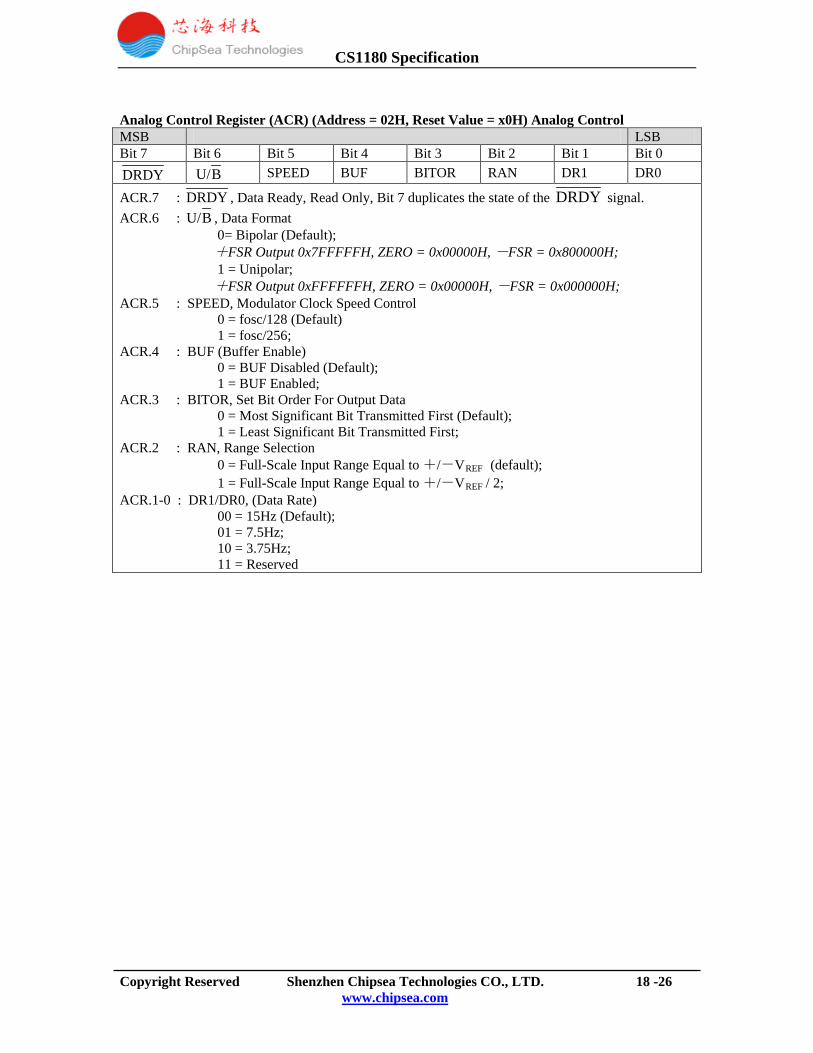
Analog Control Register (ACR) (Address = 02H, Reset Value = x0H) Analog Control MSB LSB Bit 7 Bit 6 Bit 5 Bit 4 Bit 3 Bit 2 Bit 1 Bit 0 DRDY BU/ SPEED BUF BITOR RAN DR1 DR0
ACR.7 : DRDY , Data Ready, Read Only, Bit 7 duplicates the state of the DRDY signal. ACR.6 : BU/ , Data Format 0= Bipolar (Default); +FSR Output 0x7FFFFFH, ZERO = 0x00000H, -FSR = 0x800000H; 1 = Unipolar; +FSR Output 0xFFFFFFH, ZERO = 0x00000H, -FSR = 0x000000H; ACR.5 : SPEED, Modulator Clock Speed Control 0 = fosc/128 (Default) 1 = fosc/256; ACR.4 : BUF (Buffer Enable) 0 = BUF Disabled (Default); 1 = BUF Enabled; ACR.3 : BITOR, Set Bit Order For Output Data 0 = Most Significant Bit Transmitted First (Default); 1 = Least Significant Bit Transmitted First; ACR.2 : RAN, Range Selection 0 = Full-Scale Input Range Equal to +/-VREF
1 = Full-Scale Input Range Equal to +/-V (default);
REF ACR.1-0 : DR1/DR0, (Data Rate)
/ 2;
00 = 15Hz (Default); 01 = 7.5Hz; 10 = 3.75Hz; 11 = Reserved
CS1180 Specification
Copyright Reserved Shenzhen Chipsea Technologies CO., LTD. 19 -26
www.chipsea.com
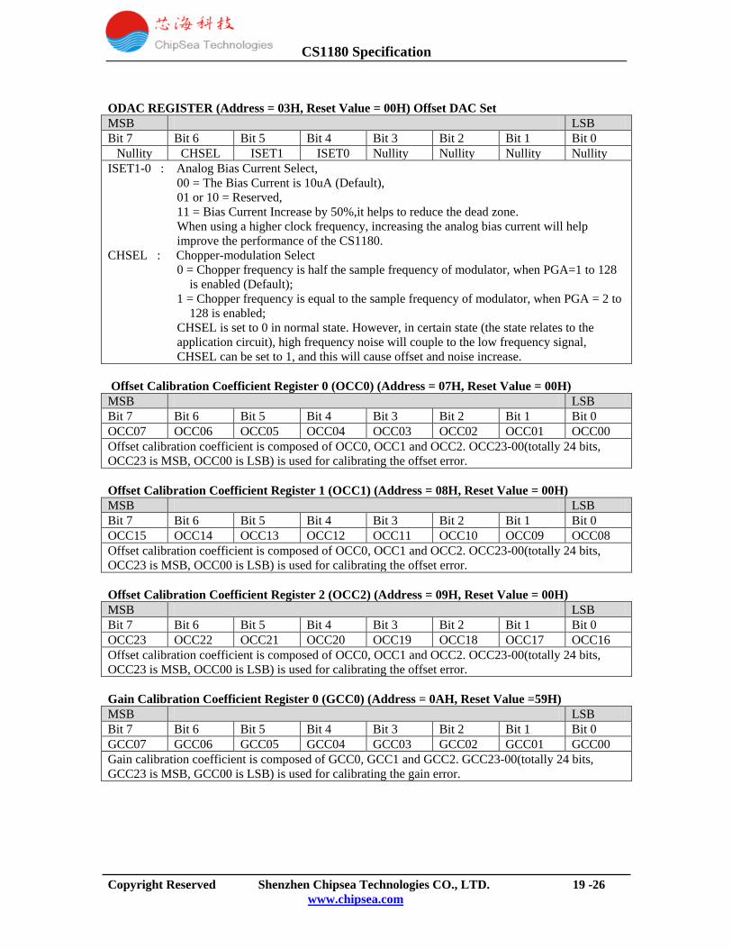
ODAC REGISTER (Address = 03H, Reset Value = 00H) Offset DAC Set MSB LSB Bit 7 Bit 6 Bit 5 Bit 4 Bit 3 Bit 2 Bit 1 Bit 0
Nullity CHSEL ISET1 ISET0 Nullity Nullity Nullity Nullity ISET1-0 : Analog Bias Current Select, 00 = The Bias Current is 10uA (Default),
01 or 10 = Reserved, 11 = Bias Current Increase by 50%,it helps to reduce the dead zone. When using a higher clock frequency, increasing the analog bias current will help improve the performance of the CS1180.
CHSEL : Chopper-modulation Select 0 = Chopper frequency is half the sample frequency of modulator, when PGA=1 to 128
is enabled (Default); 1 = Chopper frequency is equal to the sample frequency of modulator, when PGA = 2 to
128 is enabled; CHSEL is set to 0 in normal state. However, in certain state (the state relates to the application circuit), high frequency noise will couple to the low frequency signal, CHSEL can be set to 1, and this will cause offset and noise increase.
Offset Calibration Coefficient Register 0 (OCC0) (Address = 07H, Reset Value = 00H) MSB LSB Bit 7 Bit 6 Bit 5 Bit 4 Bit 3 Bit 2 Bit 1 Bit 0 OCC07 OCC06 OCC05 OCC04 OCC03 OCC02 OCC01 OCC00 Offset calibration coefficient is composed of OCC0, OCC1 and OCC2. OCC23-00(totally 24 bits, OCC23 is MSB, OCC00 is LSB) is used for calibrating the offset error. Offset Calibration Coefficient Register 1 (OCC1) (Address = 08H, Reset Value = 00H) MSB LSB Bit 7 Bit 6 Bit 5 Bit 4 Bit 3 Bit 2 Bit 1 Bit 0 OCC15 OCC14 OCC13 OCC12 OCC11 OCC10 OCC09 OCC08 Offset calibration coefficient is composed of OCC0, OCC1 and OCC2. OCC23-00(totally 24 bits, OCC23 is MSB, OCC00 is LSB) is used for calibrating the offset error. Offset Calibration Coefficient Register 2 (OCC2) (Address = 09H, Reset Value = 00H) MSB LSB Bit 7 Bit 6 Bit 5 Bit 4 Bit 3 Bit 2 Bit 1 Bit 0 OCC23 OCC22 OCC21 OCC20 OCC19 OCC18 OCC17 OCC16 Offset calibration coefficient is composed of OCC0, OCC1 and OCC2. OCC23-00(totally 24 bits, OCC23 is MSB, OCC00 is LSB) is used for calibrating the offset error. Gain Calibration Coefficient Register 0 (GCC0) (Address = 0AH, Reset Value =59H) MSB LSB Bit 7 Bit 6 Bit 5 Bit 4 Bit 3 Bit 2 Bit 1 Bit 0 GCC07 GCC06 GCC05 GCC04 GCC03 GCC02 GCC01 GCC00 Gain calibration coefficient is composed of GCC0, GCC1 and GCC2. GCC23-00(totally 24 bits, GCC23 is MSB, GCC00 is LSB) is used for calibrating the gain error.
CS1180 Specification
Copyright Reserved Shenzhen Chipsea Technologies CO., LTD. 20 -26
www.chipsea.com
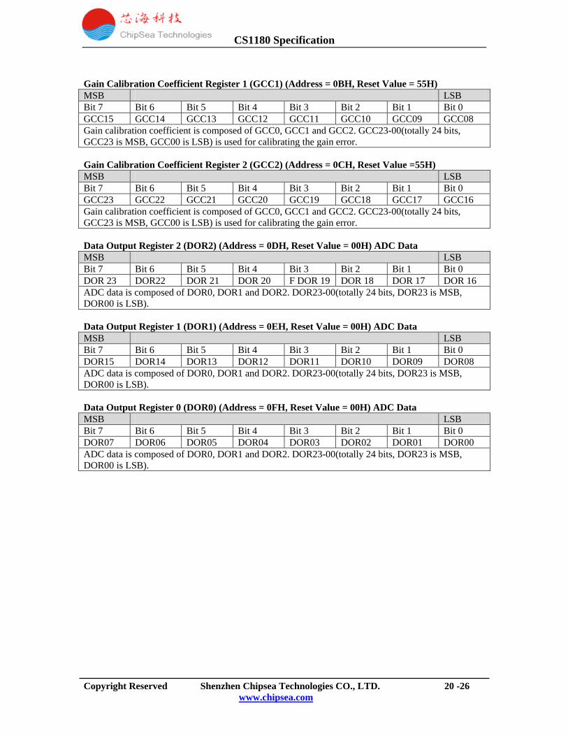
Gain Calibration Coefficient Register 1 (GCC1) (Address = 0BH, Reset Value = 55H) MSB LSB Bit 7 Bit 6 Bit 5 Bit 4 Bit 3 Bit 2 Bit 1 Bit 0 GCC15 GCC14 GCC13 GCC12 GCC11 GCC10 GCC09 GCC08 Gain calibration coefficient is composed of GCC0, GCC1 and GCC2. GCC23-00(totally 24 bits, GCC23 is MSB, GCC00 is LSB) is used for calibrating the gain error. Gain Calibration Coefficient Register 2 (GCC2) (Address = 0CH, Reset Value =55H) MSB LSB Bit 7 Bit 6 Bit 5 Bit 4 Bit 3 Bit 2 Bit 1 Bit 0 GCC23 GCC22 GCC21 GCC20 GCC19 GCC18 GCC17 GCC16 Gain calibration coefficient is composed of GCC0, GCC1 and GCC2. GCC23-00(totally 24 bits, GCC23 is MSB, GCC00 is LSB) is used for calibrating the gain error. Data Output Register 2 (DOR2) (Address = 0DH, Reset Value = 00H) ADC Data MSB LSB Bit 7 Bit 6 Bit 5 Bit 4 Bit 3 Bit 2 Bit 1 Bit 0 DOR 23 DOR22 DOR 21 DOR 20 F DOR 19 DOR 18 DOR 17 DOR 16 ADC data is composed of DOR0, DOR1 and DOR2. DOR23-00(totally 24 bits, DOR23 is MSB, DOR00 is LSB). Data Output Register 1 (DOR1) (Address = 0EH, Reset Value = 00H) ADC Data MSB LSB Bit 7 Bit 6 Bit 5 Bit 4 Bit 3 Bit 2 Bit 1 Bit 0 DOR15 DOR14 DOR13 DOR12 DOR11 DOR10 DOR09 DOR08 ADC data is composed of DOR0, DOR1 and DOR2. DOR23-00(totally 24 bits, DOR23 is MSB, DOR00 is LSB). Data Output Register 0 (DOR0) (Address = 0FH, Reset Value = 00H) ADC Data MSB LSB Bit 7 Bit 6 Bit 5 Bit 4 Bit 3 Bit 2 Bit 1 Bit 0 DOR07 DOR06 DOR05 DOR04 DOR03 DOR02 DOR01 DOR00 ADC data is composed of DOR0, DOR1 and DOR2. DOR23-00(totally 24 bits, DOR23 is MSB, DOR00 is LSB).
CS1180 Specification
Copyright Reserved Shenzhen Chipsea Technologies CO., LTD. 21 -26
www.chipsea.com
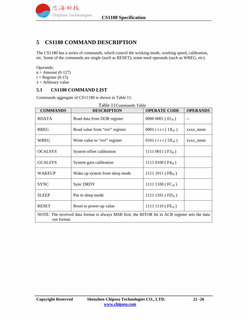
5 CS1180 COMMAND DESCRIPTION
The CS1180 has a series of commands, which control the working mode, working speed, calibration, etc. Some of the commands are single (such as RESET); some need operands (such as WREG, etc). Operands: n = Amount (0-127) r = Register (0-15) x = Arbitrary value
5.1 CS1180 COMMAND LIST Commands aggregate of CS11180 is shown in Table 11.
Table 11 Commands Table COMMANDS DESCRIPTION OPERATE CODE OPERANDS
RDATA Read data from DOR register 0000 0001 ( 01H -- )
RREG Read value from “rrrr” register 0001 r r r r ( 1XH xxxx_nnnn )
WREG Write value to “rrrr” register 0101 r r r r ( 5XH xxxx_nnnn )
OCALSYS System offset calibration 1111 0011 ( F3H )
GCALSYS System gain calibration 1111 0100 ( F4H )
WAKEUP Wake up system from sleep mode 1111 1011 ( FBH )
SYNC Sync DRDY 1111 1100 ( FCH )
SLEEP Put in sleep mode 1111 1101 ( FDH )
RESET Reset to power-up value 1111 1110 ( FEH )
NOTE: The received data format is always MSB first; the BITOR bit in ACR register sets the data out format.
CS1180 Specification
Copyright Reserved Shenzhen Chipsea Technologies CO., LTD. 22 -26
www.chipsea.com
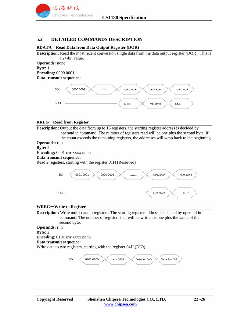
5.2 DETAILED COMMANDS DESCRIPTION RDATA-Read Data from Data Output Register (DOR) Description: Read the most recent conversion single data from the data output register (DOR). This is
a 24-bit value. Operands: none Byte: 1 Encoding: 0000 0001 Data transmit sequence: RREG-Read from Register Description: Output the data from up to 16 registers, the starting register address is decided by
operand in command. The number of registers read will be one plus the second byte. If the count exceeds the remaining registers, the addresses will wrap back to the beginning.
Operands: r, n Byte: 2 Encoding: 0001 rrrr xxxx nnnn Data transmit sequence: Read 2 registers, starting with the register 01H (Reserved) WREG-Write to Register Description: Write multi-data to registers. The starting register address is decided by operand in
command. The number of registers that will be written is one plus the value of the second byte.
Operands: r, n Byte: 2 Encoding: 0101 rrrr xxxx nnnn Data transmit sequence: Write data to two registers, starting with the register 04H (DIO)
Reserved ACR
xxxx xxxx xxxx xxxx 0001 0001 …….. 0000 0001 SDI
SDO
MSB Mid-Byte LSB
xxxx xxxx xxxx xxxx 0000 0001 xxxx xxxx …….. SDI
SDO
0101 0100 xxxx 0001 Data for DIO Data For DIR SDI
CS1180 Specification
Copyright Reserved Shenzhen Chipsea Technologies CO., LTD. 23 -26
www.chipsea.com
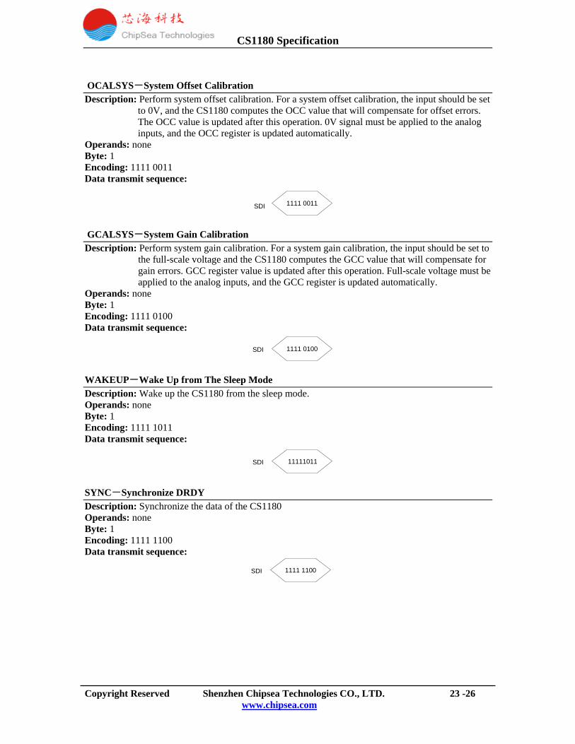
OCALSYS-System Offset Calibration Description: Perform system offset calibration. For a system offset calibration, the input should be set
to 0V, and the CS1180 computes the OCC value that will compensate for offset errors. The OCC value is updated after this operation. 0V signal must be applied to the analog inputs, and the OCC register is updated automatically.
Operands: none Byte: 1 Encoding: 1111 0011 Data transmit sequence:
GCALSYS-System Gain Calibration Description: Perform system gain calibration. For a system gain calibration, the input should be set to
the full-scale voltage and the CS1180 computes the GCC value that will compensate for gain errors. GCC register value is updated after this operation. Full-scale voltage must be applied to the analog inputs, and the GCC register is updated automatically.
Operands: none Byte: 1 Encoding: 1111 0100 Data transmit sequence:
WAKEUP-Wake Up from The Sleep Mode Description: Wake up the CS1180 from the sleep mode. Operands: none Byte: 1 Encoding: 1111 1011 Data transmit sequence:
SYNC-Synchronize DRDY Description: Synchronize the data of the CS1180 Operands: none Byte: 1 Encoding: 1111 1100 Data transmit sequence:
1111 0011 SDI
1111 0100 SDI
11111011 SDI
1111 1100 SDI
CS1180 Specification
Copyright Reserved Shenzhen Chipsea Technologies CO., LTD. 24 -26
www.chipsea.com
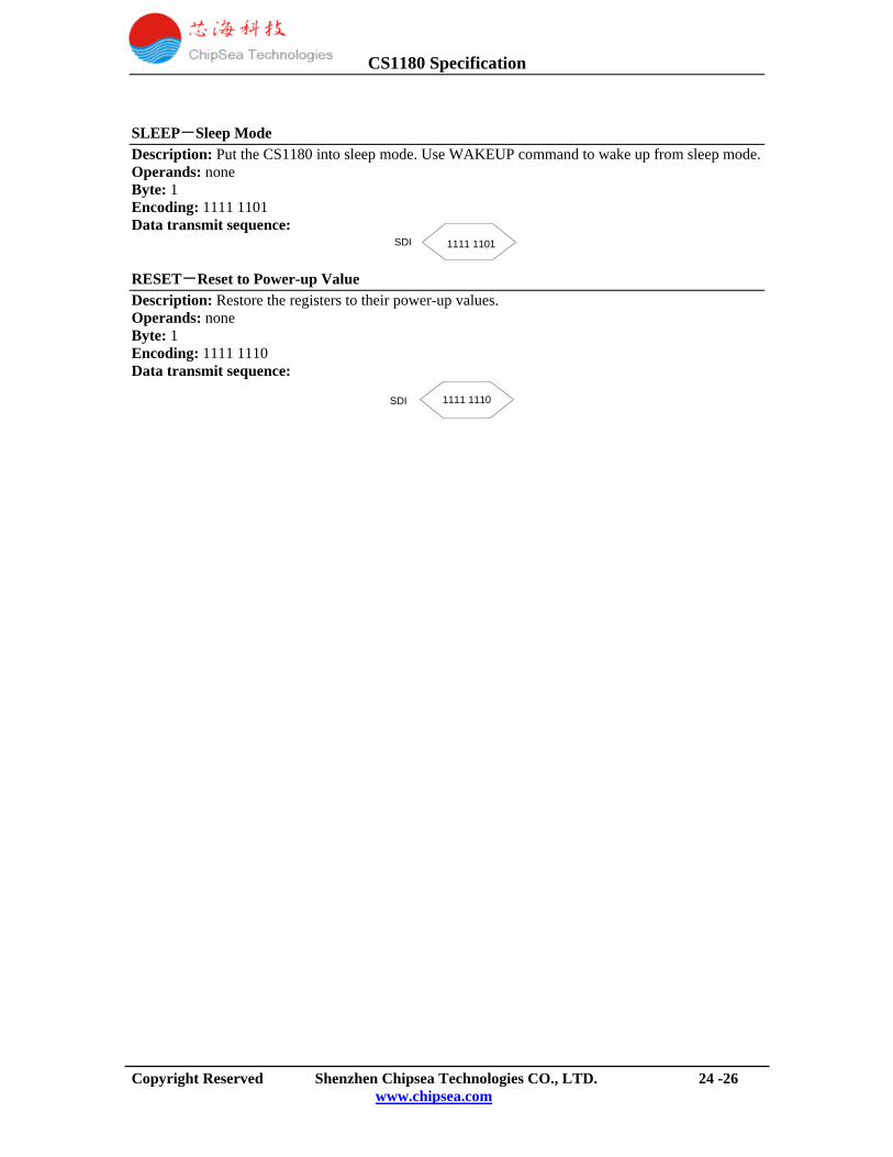
SLEEP-Sleep Mode Description: Put the CS1180 into sleep mode. Use WAKEUP command to wake up from sleep mode. Operands: none Byte: 1 Encoding: 1111 1101 Data transmit sequence: RESET-Reset to Power-up Value Description: Restore the registers to their power-up values. Operands: none Byte: 1 Encoding: 1111 1110 Data transmit sequence:
1111 1101 SDI
1111 1110 SDI

CS1180 Specification
Copyright Reserved Shenzhen Chipsea Technologies CO., LTD. 25 -26
www.chipsea.com
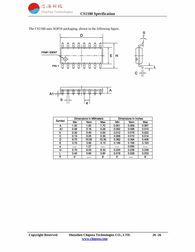
6 CS1180 PACKAGE
The CS1180 uses SSOP16 packaging, shown in the following figure.
CS1180 Specification
Copyright Reserved Shenzhen Chipsea Technologies CO., LTD. 26 -26
www.chipsea.com
The CS1180 uses SOP16 packaging, shown in the following figure.