Embed Size (px)
Citation preview
CS 3510 CS 3510 Comp&NetComp&Net ArchArch
Transistors & Gates
Dr. Ken Hoganson © 2010
CS 3510 CS 3510 Comp&NetComp&Net Arch. Dr. Ken Hoganson, Copyright Arch. Dr. Ken Hoganson, Copyright ©© 20102010
3-Input AND from Transistors
Illustrates construction of gatesIllustrates the “transistor bleed-through” problem that affects the AND circuit.Illustrates basic use of IDL-800
CS 3510 CS 3510 Comp&NetComp&Net Arch. Dr. Ken Hoganson, Copyright Arch. Dr. Ken Hoganson, Copyright ©© 20102010
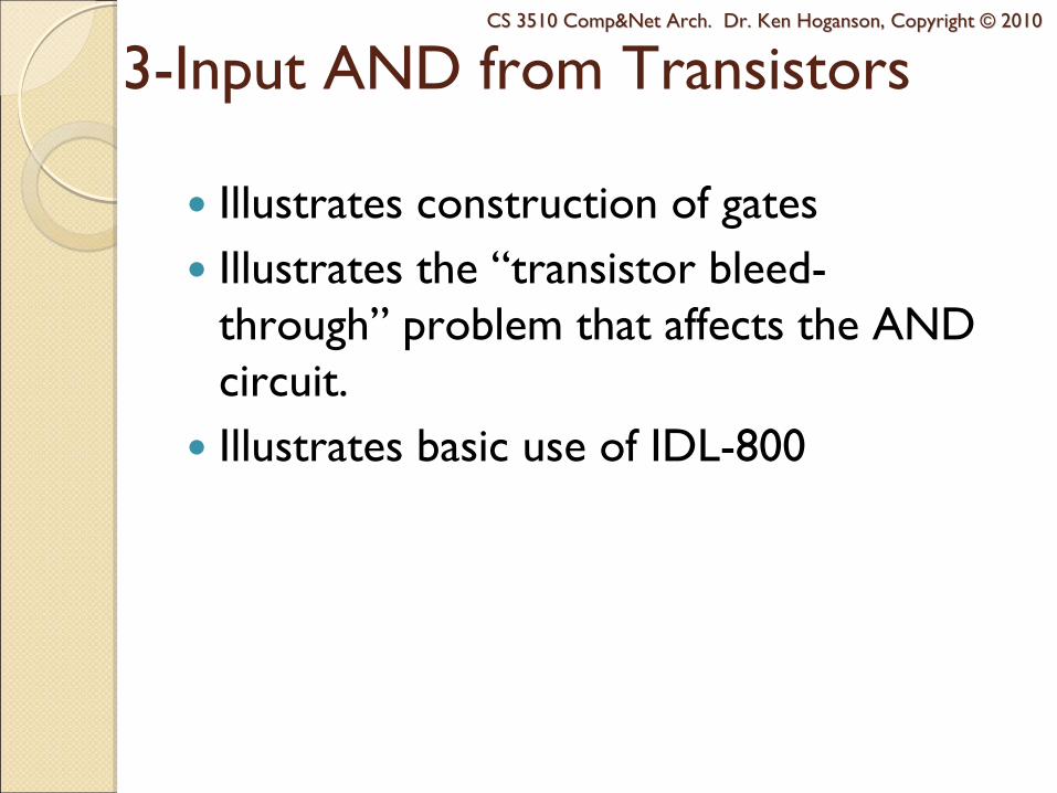
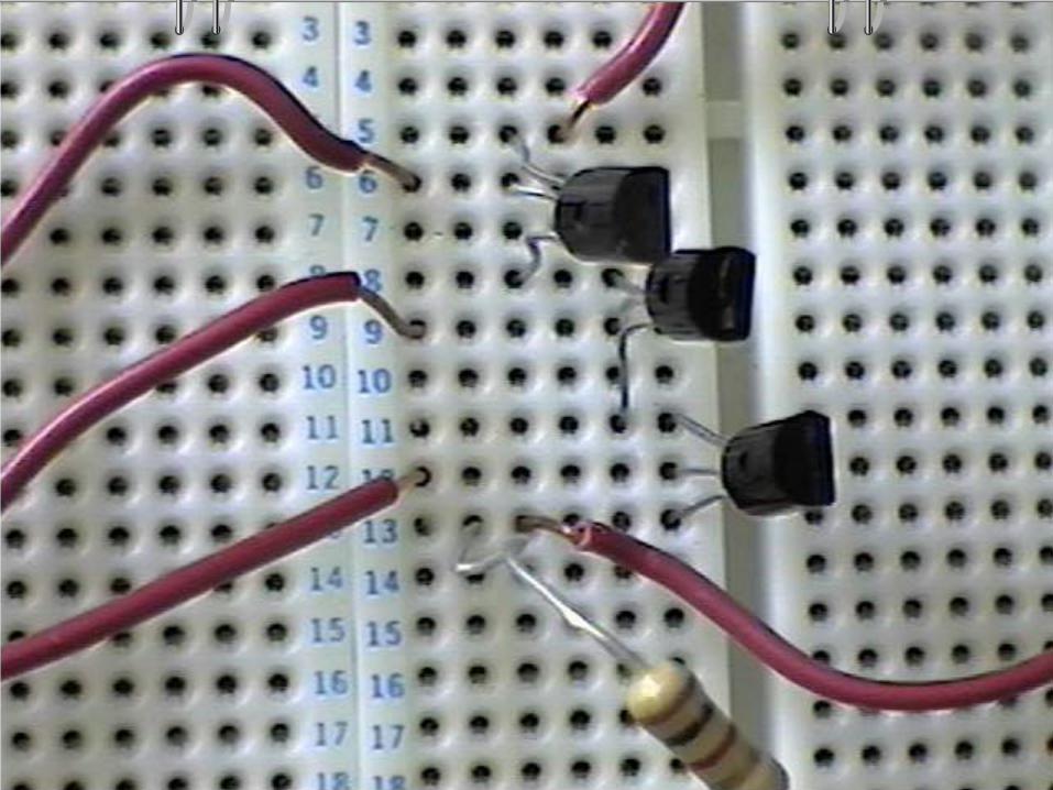
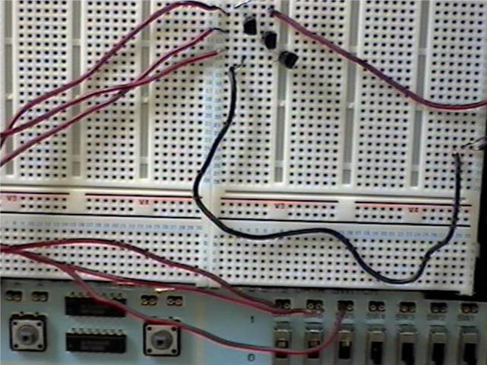
Transistors in Series
A
B
Out
C
V+• Construction of 3-Input (A,B,C)
AND from transistors.
• Note the resistor and output are at the “bottom”.
• Three inputs (from switches)
CS 3510 CS 3510 Comp&NetComp&Net Arch. Dr. Ken Hoganson, Copyright Arch. Dr. Ken Hoganson, Copyright ©© 20102010
CS 3510 CS 3510 Comp&NetComp&Net Arch. Dr. Ken Hoganson, Copyright Arch. Dr. Ken Hoganson, Copyright ©© 20102010
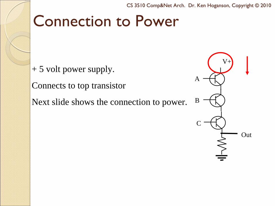
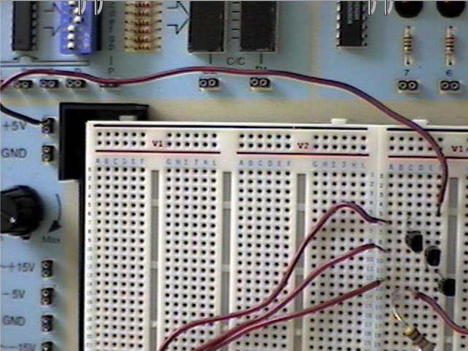
Connection to Power
+ 5 volt power supply.
Connects to top transistor
Next slide shows the connection to power.
A
B
Out
C
V+
CS 3510 CS 3510 Comp&NetComp&Net Arch. Dr. Ken Hoganson, Copyright Arch. Dr. Ken Hoganson, Copyright ©© 20102010
CS 3510 CS 3510 Comp&NetComp&Net Arch. Dr. Ken Hoganson, Copyright Arch. Dr. Ken Hoganson, Copyright ©© 20102010
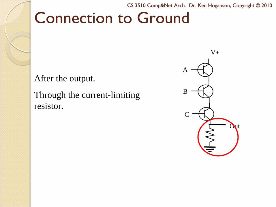
Connection to Ground
A
B
Out
C
V+
After the output.
Through the current-limiting resistor.
CS 3510 CS 3510 Comp&NetComp&Net Arch. Dr. Ken Hoganson, Copyright Arch. Dr. Ken Hoganson, Copyright ©© 20102010
CS 3510 CS 3510 Comp&NetComp&Net Arch. Dr. Ken Hoganson, Copyright Arch. Dr. Ken Hoganson, Copyright ©© 20102010
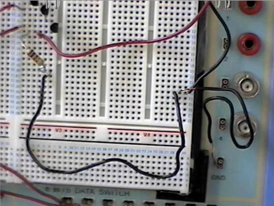
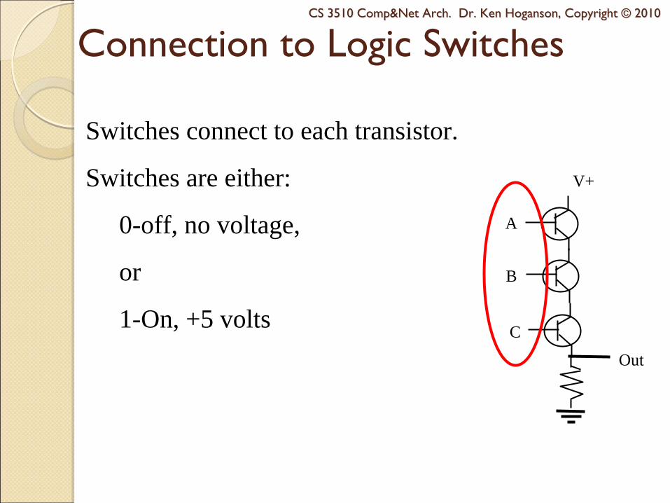
Connection to Logic Switches
A
B
Out
C
V+
Switches connect to each transistor.
Switches are either:
0-off, no voltage,
or
1-On, +5 volts
CS 3510 CS 3510 Comp&NetComp&Net Arch. Dr. Ken Hoganson, Copyright Arch. Dr. Ken Hoganson, Copyright ©© 20102010
CS 3510 CS 3510 Comp&NetComp&Net Arch. Dr. Ken Hoganson, Copyright Arch. Dr. Ken Hoganson, Copyright ©© 20102010
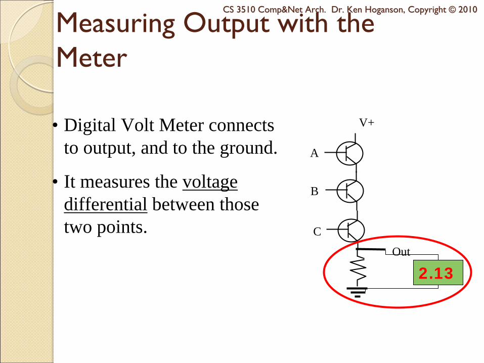
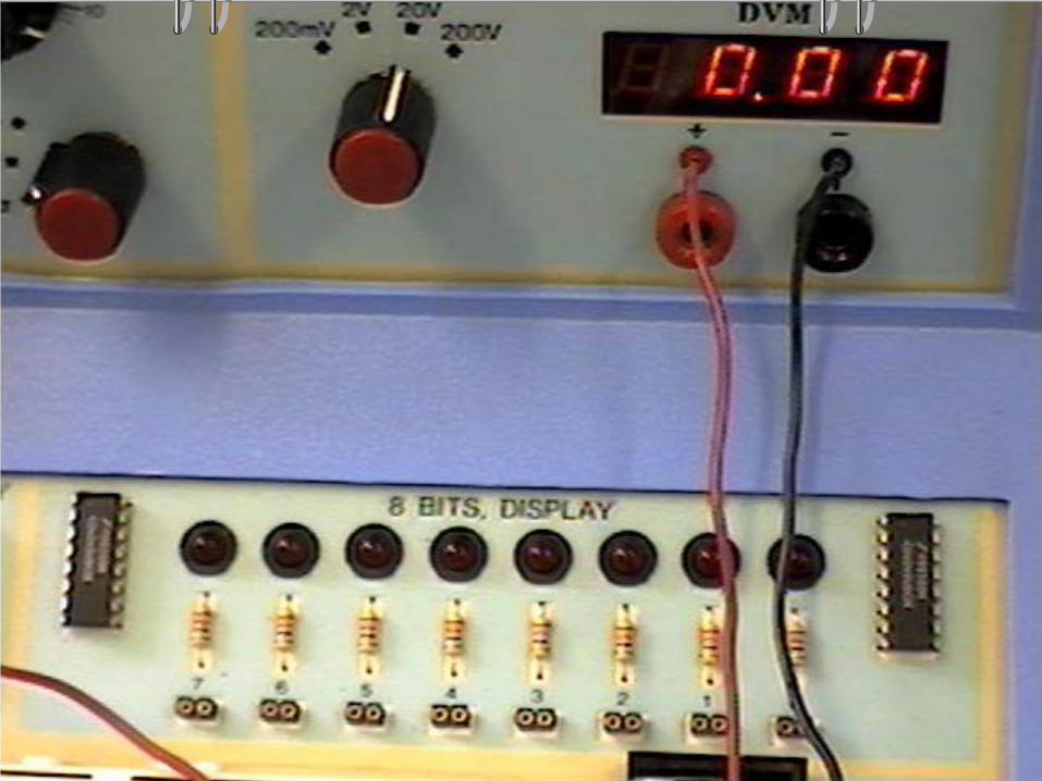
Measuring Output with the Meter
A
B
Out
C
V+
2.13
• Digital Volt Meter connects to output, and to the ground.
• It measures the voltage differential between those two points.
CS 3510 CS 3510 Comp&NetComp&Net Arch. Dr. Ken Hoganson, Copyright Arch. Dr. Ken Hoganson, Copyright ©© 20102010
CS 3510 CS 3510 Comp&NetComp&Net Arch. Dr. Ken Hoganson, Copyright Arch. Dr. Ken Hoganson, Copyright ©© 20102010
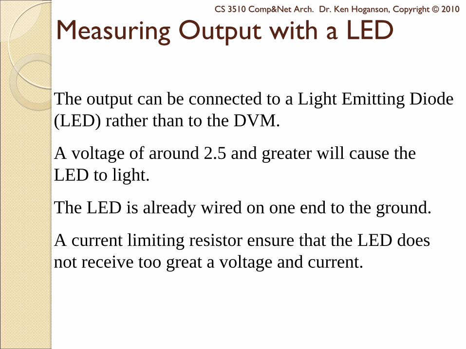
Measuring Output with a LED
The output can be connected to a Light Emitting Diode (LED) rather than to the DVM.
A voltage of around 2.5 and greater will cause the LED to light.
The LED is already wired on one end to the ground.
A current limiting resistor ensure that the LED does not receive too great a voltage and current.
CS 3510 CS 3510 Comp&NetComp&Net Arch. Dr. Ken Hoganson, Copyright Arch. Dr. Ken Hoganson, Copyright ©© 20102010
CS 3510 CS 3510 Comp&NetComp&Net Arch. Dr. Ken Hoganson, Copyright Arch. Dr. Ken Hoganson, Copyright ©© 20102010
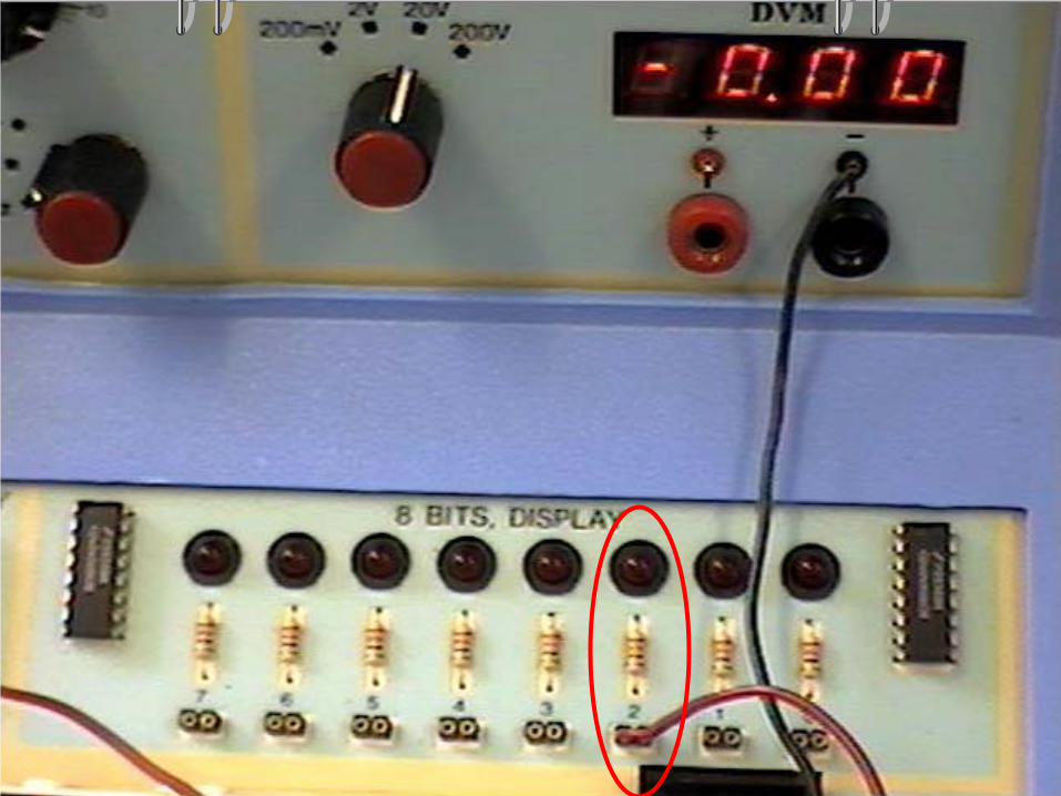
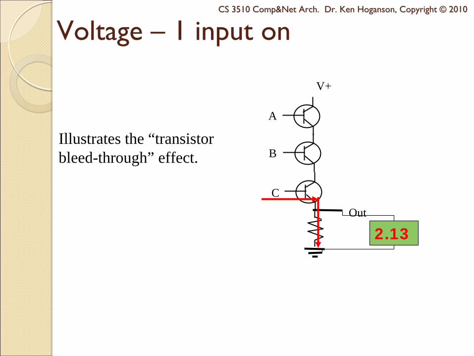
Voltage – 1 input on
A
B
Out
C
V+
2.13
Illustrates the “transistor bleed-through” effect.

CS 3510 CS 3510 Comp&NetComp&Net Arch. Dr. Ken Hoganson, Copyright Arch. Dr. Ken Hoganson, Copyright ©© 20102010
CS 3510 CS 3510 Comp&NetComp&Net Arch. Dr. Ken Hoganson, Copyright Arch. Dr. Ken Hoganson, Copyright ©© 20102010
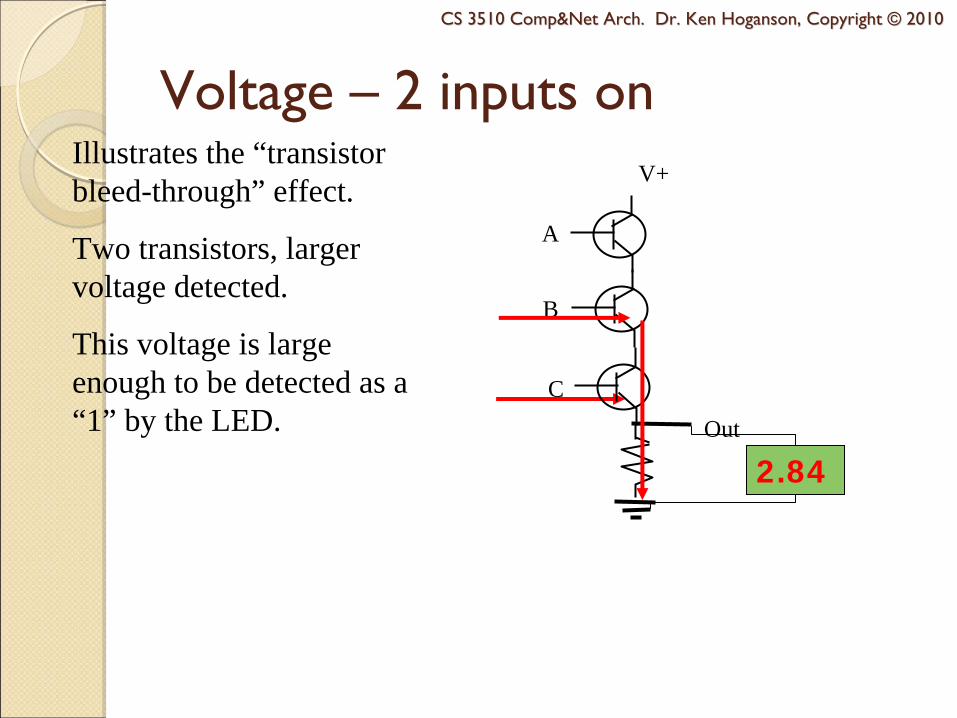
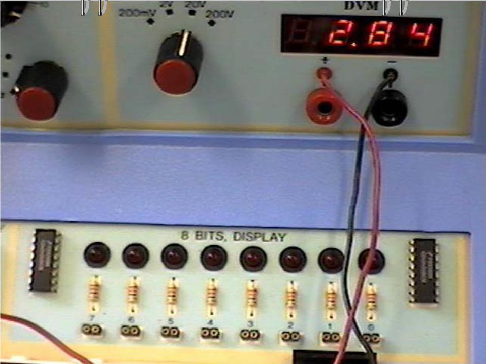
Voltage – 2 inputs on
A
B
Out
C
V+
2.84
Illustrates the “transistor bleed-through” effect.
Two transistors, larger voltage detected.
This voltage is large enough to be detected as a “1” by the LED.
CS 3510 CS 3510 Comp&NetComp&Net Arch. Dr. Ken Hoganson, Copyright Arch. Dr. Ken Hoganson, Copyright ©© 20102010
CS 3510 CS 3510 Comp&NetComp&Net Arch. Dr. Ken Hoganson, Copyright Arch. Dr. Ken Hoganson, Copyright ©© 20102010
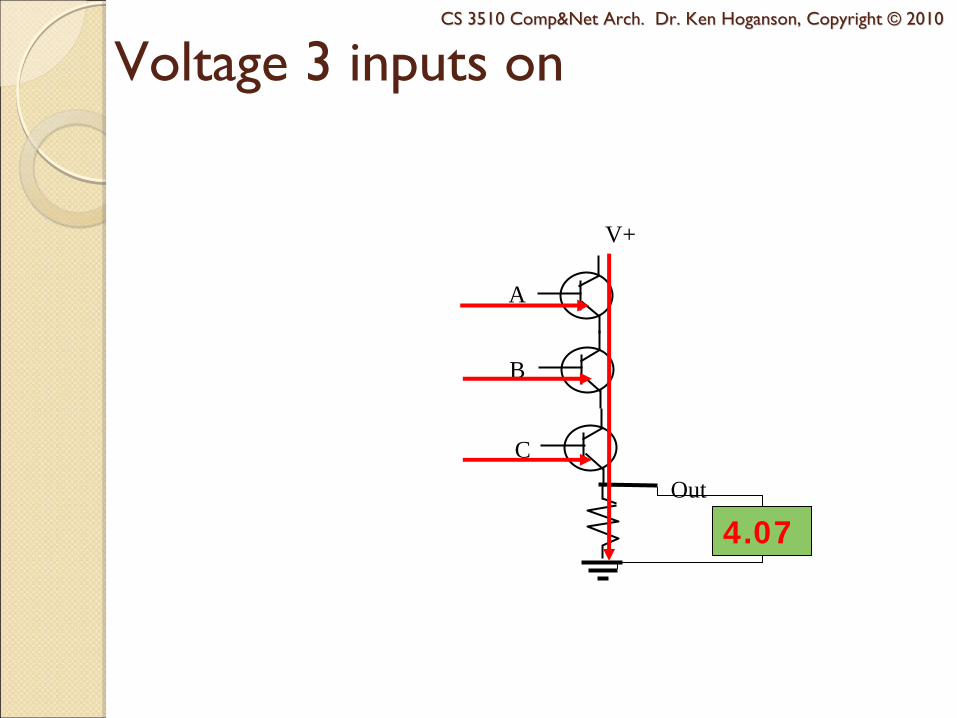
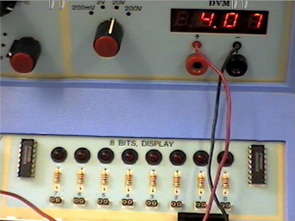
Voltage 3 inputs on
A
B
Out
C
V+
4.07
CS 3510 CS 3510 Comp&NetComp&Net Arch. Dr. Ken Hoganson, Copyright Arch. Dr. Ken Hoganson, Copyright ©© 20102010
CS 3510 CS 3510 Comp&NetComp&Net Arch. Dr. Ken Hoganson, Copyright Arch. Dr. Ken Hoganson, Copyright ©© 20102010
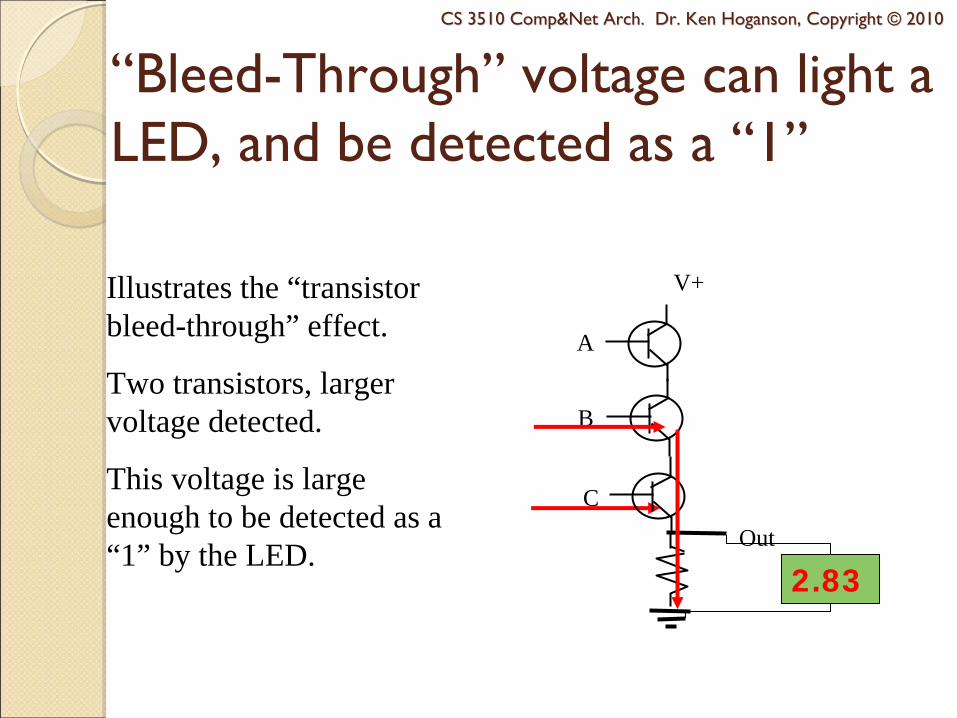
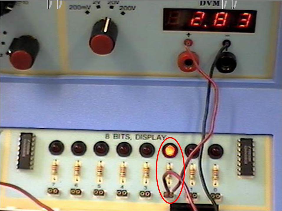
“Bleed-Through” voltage can light a LED, and be detected as a “1”
A
B
Out
C
V+
2.83
Illustrates the “transistor bleed-through” effect.
Two transistors, larger voltage detected.
This voltage is large enough to be detected as a “1” by the LED.
CS 3510 CS 3510 Comp&NetComp&Net Arch. Dr. Ken Hoganson, Copyright Arch. Dr. Ken Hoganson, Copyright ©© 20102010
CS 3510 CS 3510 Comp&NetComp&Net Arch. Dr. Ken Hoganson, Copyright Arch. Dr. Ken Hoganson, Copyright ©© 20102010
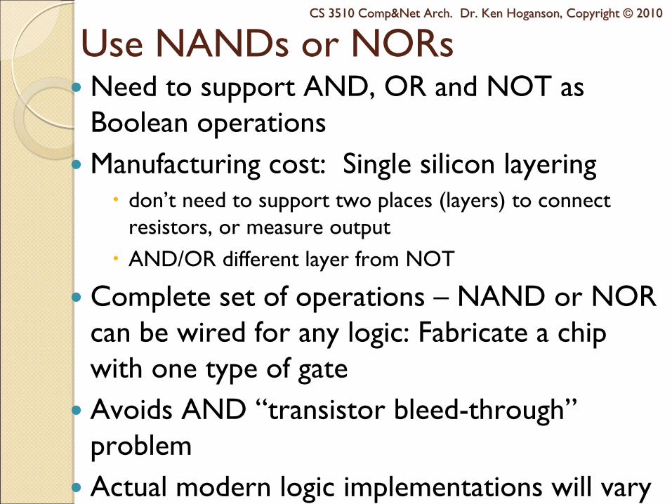
Use NANDs or NORsNeed to support AND, OR and NOT as Boolean operationsManufacturing cost: Single silicon layering
don’t need to support two places (layers) to connect resistors, or measure outputAND/OR different layer from NOT
Complete set of operations – NAND or NOR can be wired for any logic: Fabricate a chip with one type of gateAvoids AND “transistor bleed-through”problemActual modern logic implementations will vary
CS 3510 CS 3510 Comp&NetComp&Net Arch. Dr. Ken Hoganson, Copyright Arch. Dr. Ken Hoganson, Copyright ©© 20102010
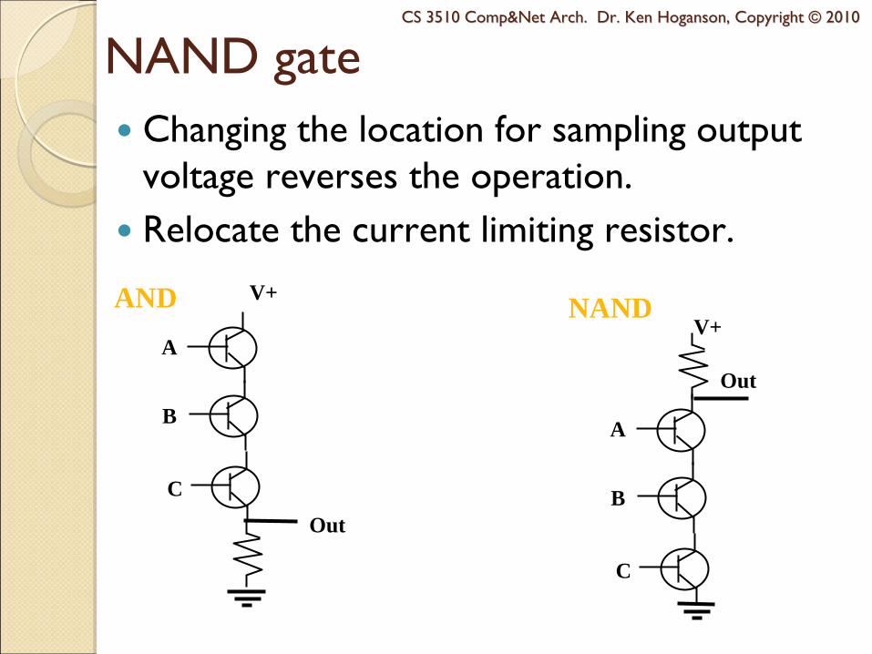
NAND gateChanging the location for sampling output voltage reverses the operation.Relocate the current limiting resistor.
A
B
Out
C
V+
Out
A
B
C
V+AND NAND
CS 3510 CS 3510 Comp&NetComp&Net Arch. Dr. Ken Hoganson, Copyright Arch. Dr. Ken Hoganson, Copyright ©© 20102010
CS 3510 CS 3510 Comp&NetComp&Net Arch. Dr. Ken Hoganson, Copyright Arch. Dr. Ken Hoganson, Copyright ©© 20102010
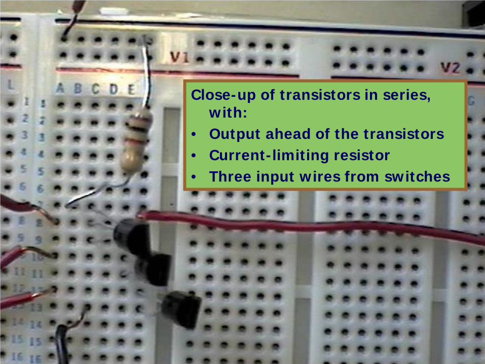
Close-up of transistors in series, with:
• Output ahead of the transistors• Current-limiting resistor• Three input wires from switches
CS 3510 CS 3510 Comp&NetComp&Net Arch. Dr. Ken Hoganson, Copyright Arch. Dr. Ken Hoganson, Copyright ©© 20102010
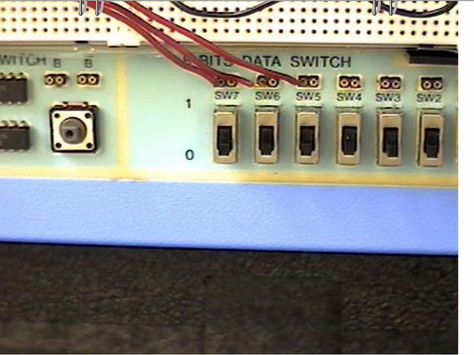
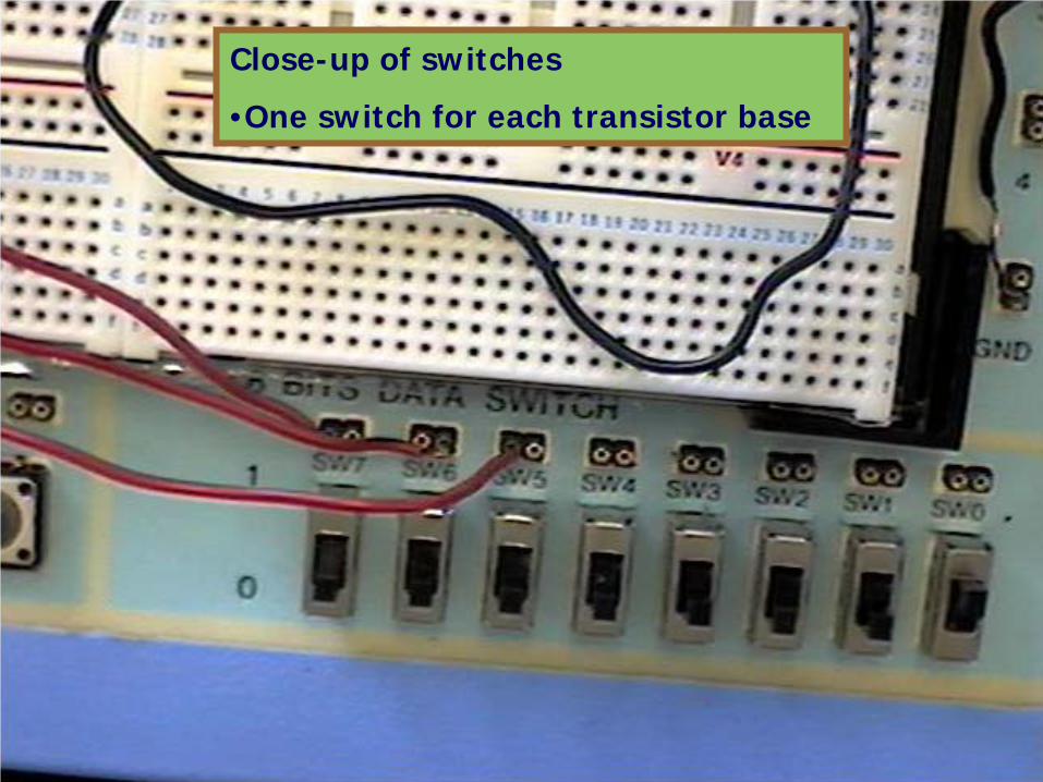
Close-up of switches
•One switch for each transistor base
CS 3510 CS 3510 Comp&NetComp&Net Arch. Dr. Ken Hoganson, Copyright Arch. Dr. Ken Hoganson, Copyright ©© 20102010
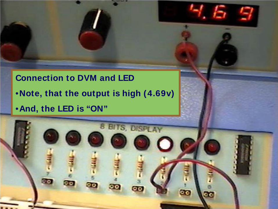
Connection to DVM and LED
•Note, that the output is high (4.69v)
•And, the LED is “ON”
CS 3510 CS 3510 Comp&NetComp&Net Arch. Dr. Ken Hoganson, Copyright Arch. Dr. Ken Hoganson, Copyright ©© 20102010
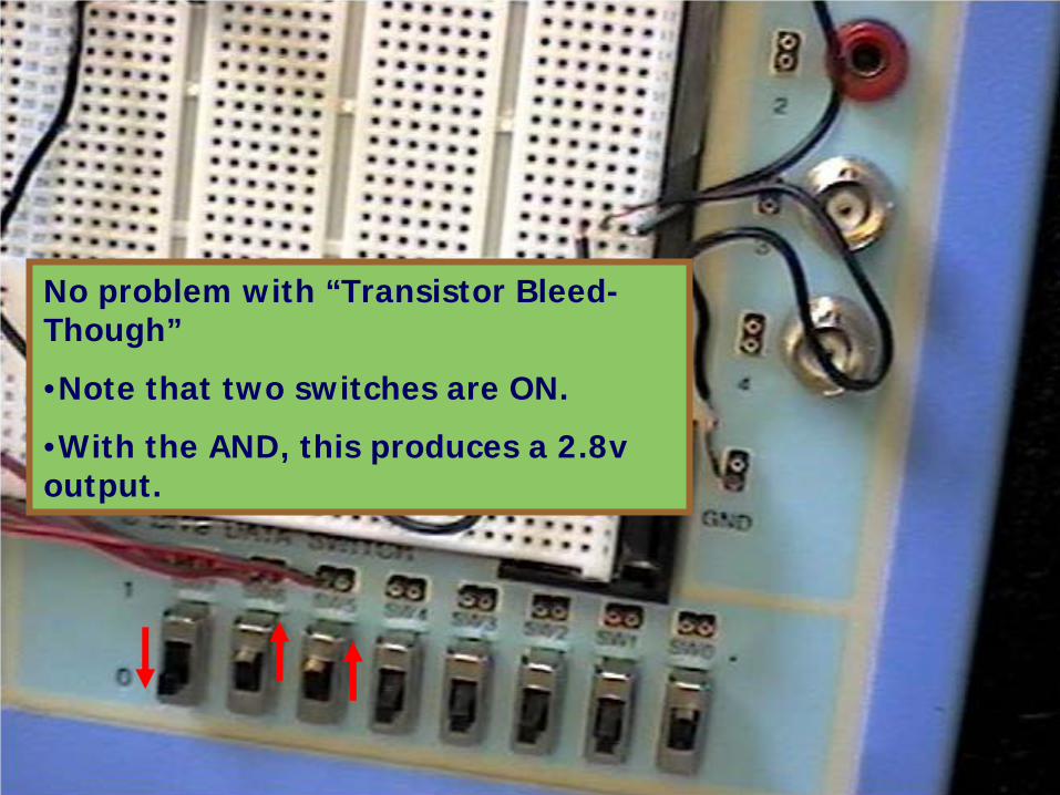
No problem with “Transistor Bleed-Though”
•Note that two switches are ON.
•With the AND, this produces a 2.8v output.
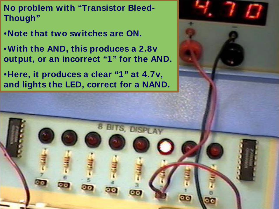
CS 3510 CS 3510 Comp&NetComp&Net Arch. Dr. Ken Hoganson, Copyright Arch. Dr. Ken Hoganson, Copyright ©© 20102010No problem with “Transistor Bleed-Though”
•Note that two switches are ON.
•With the AND, this produces a 2.8v output, or an incorrect “1” for the AND.
•Here, it produces a clear “1” at 4.7v, and lights the LED, correct for a NAND.
CS 3510 CS 3510 Comp&NetComp&Net Arch. Dr. Ken Hoganson, Copyright Arch. Dr. Ken Hoganson, Copyright ©© 20102010
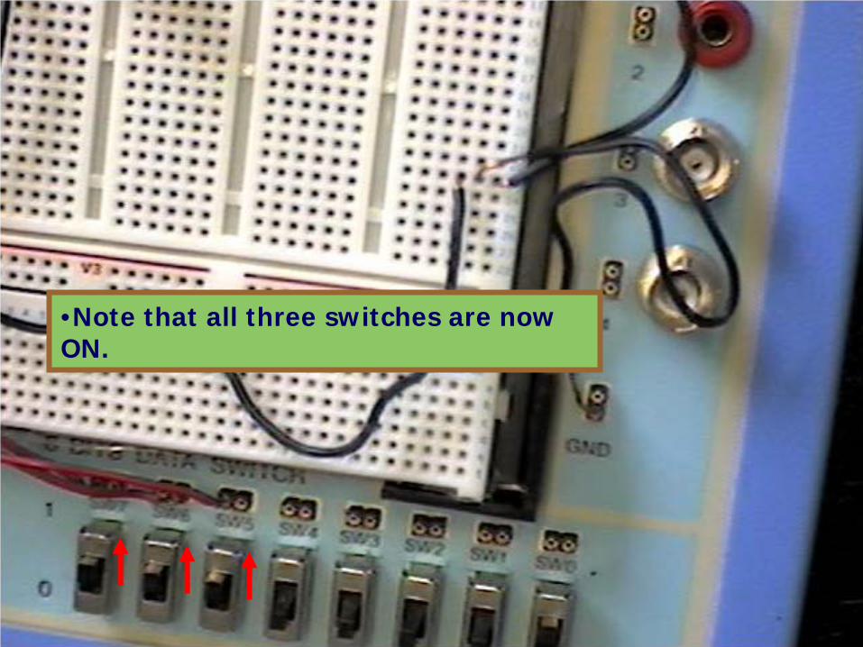
•Note that all three switches are now ON.
CS 3510 CS 3510 Comp&NetComp&Net Arch. Dr. Ken Hoganson, Copyright Arch. Dr. Ken Hoganson, Copyright ©© 20102010
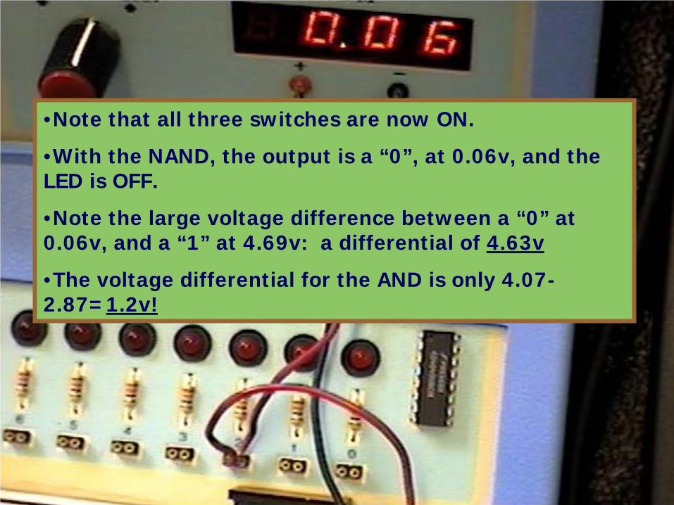
•Note that all three switches are now ON.
•With the NAND, the output is a “0”, at 0.06v, and the LED is OFF.
•Note the large voltage difference between a “0” at 0.06v, and a “1” at 4.69v: a differential of 4.63v
•The voltage differential for the AND is only 4.07-2.87=1.2v!
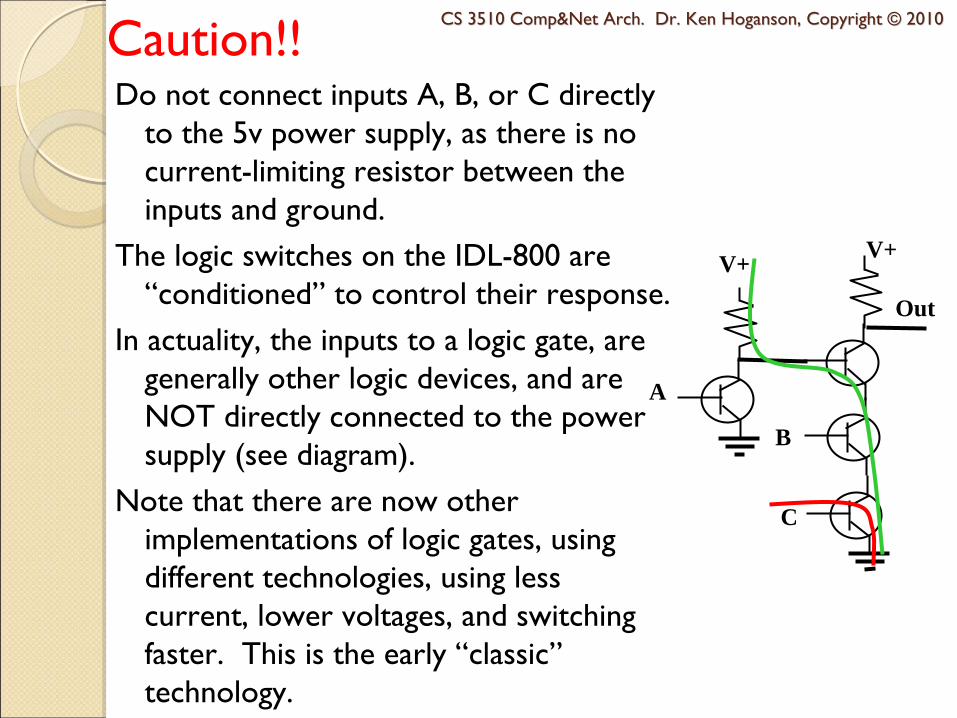
CS 3510 CS 3510 Comp&NetComp&Net Arch. Dr. Ken Hoganson, Copyright Arch. Dr. Ken Hoganson, Copyright ©© 20102010Caution!!Do not connect inputs A, B, or C directly
to the 5v power supply, as there is no current-limiting resistor between the inputs and ground.
The logic switches on the IDL-800 are “conditioned” to control their response.
In actuality, the inputs to a logic gate, are generally other logic devices, and are NOT directly connected to the power supply (see diagram).
Note that there are now other implementations of logic gates, using different technologies, using less current, lower voltages, and switching faster. This is the early “classic”technology.
Out
A
B
C
V+V+
CS 3510 CS 3510 Comp&NetComp&Net Arch. Dr. Ken Hoganson, Copyright Arch. Dr. Ken Hoganson, Copyright ©© 20102010End of LectureEnd of Lecture
End Of
Today’sLecture.

This slide intentionally left blank