Embed Size (px)
Citation preview

CS 152 L07 Single Cycle 2 (1) UC Regents Fall 2004 © UCB
2004-09-21
John Lazzaro(www.cs.berkeley.edu/~lazzaro)
Dave Patterson (www.cs.berkeley.edu/~patterson)
www-inst.eecs.berkeley.edu/~cs152/
CS152 – Computer Architecture andEngineering
Lecture 7 – (Design Notebook+)Single Cycle Control

CS 152 L07 Single Cycle 2 (2) UC Regents Fall 2004 © UCB
Review° 5 steps to design a processor
1. Analyze instruction set => datapath requirements
2. Select set of datapath components & establish clock methodology
3. Assemble datapath meeting the requirements
4. Analyze implementation of each instruction to determine setting of control points that effects the register transfer.
5. Assemble the control logic (This Lecture)
° MIPS makes it easier• Instructions same size; Source registers, immediates always in same place
• Operations always on registers/immediates
° Single cycle datapath => CPI=1, CCT => long
CS 152 L07 Single Cycle 2 (3) UC Regents Fall 2004 © UCB
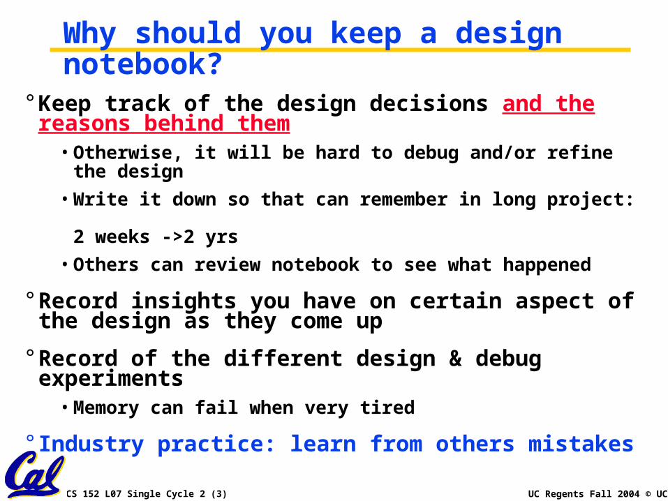
Why should you keep a design notebook?
° Keep track of the design decisions and the reasons behind them
• Otherwise, it will be hard to debug and/or refine the design
• Write it down so that can remember in long project: 2 weeks ->2 yrs
• Others can review notebook to see what happened
° Record insights you have on certain aspect of the design as they come up
° Record of the different design & debug experiments• Memory can fail when very tired
° Industry practice: learn from others mistakes
CS 152 L07 Single Cycle 2 (4) UC Regents Fall 2004 © UCB
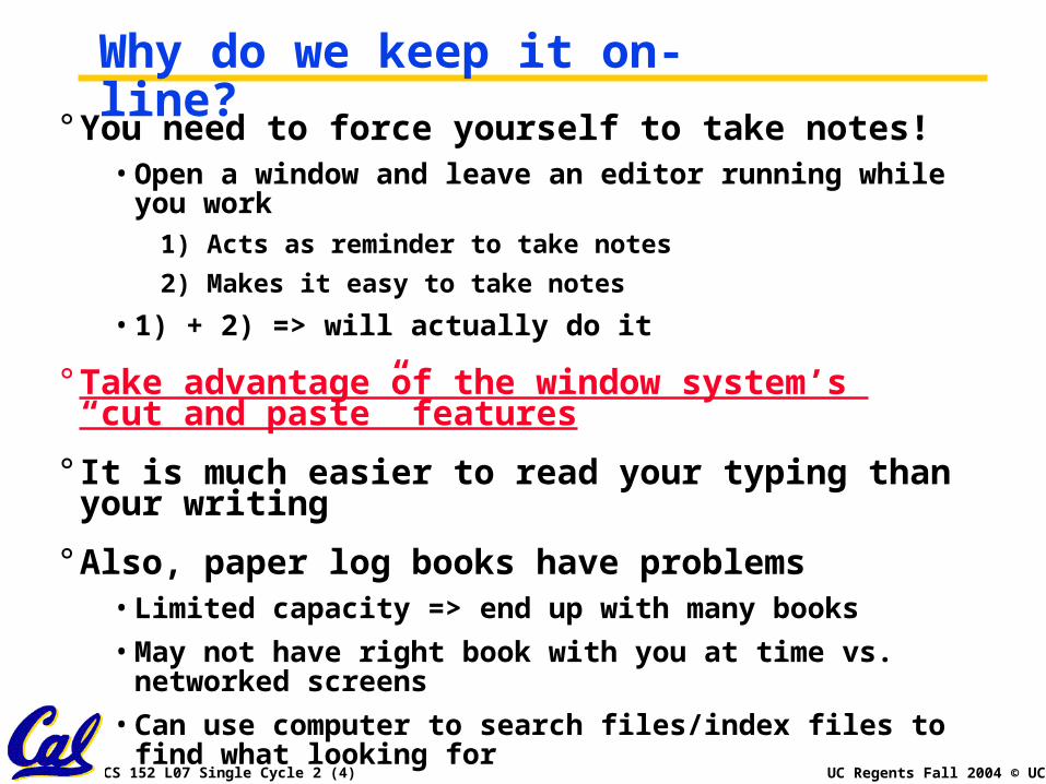
Why do we keep it on-line?
° You need to force yourself to take notes!• Open a window and leave an editor running while you work
1) Acts as reminder to take notes
2) Makes it easy to take notes
• 1) + 2) => will actually do it
° Take advantage of the window system’s “cut and paste” features
° It is much easier to read your typing than your writing
° Also, paper log books have problems• Limited capacity => end up with many books
• May not have right book with you at time vs. networked screens
• Can use computer to search files/index files to find what looking for
CS 152 L07 Single Cycle 2 (5) UC Regents Fall 2004 © UCB
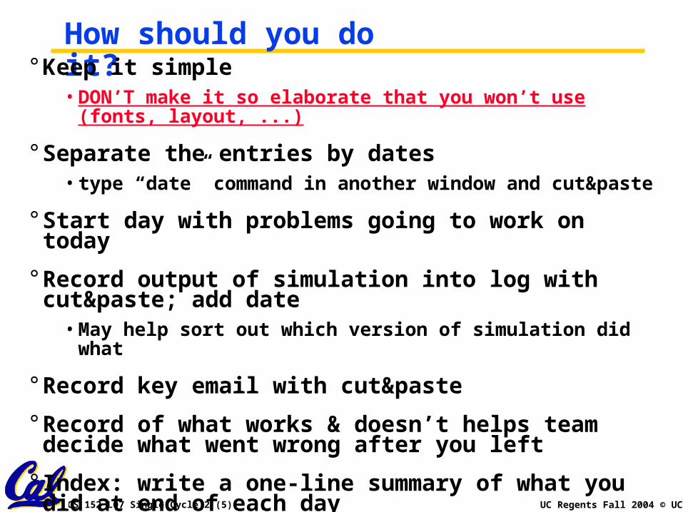
How should you do it?° Keep it simple• DON’T make it so elaborate that you won’t use (fonts, layout, ...)
° Separate the entries by dates• type “date” command in another window and cut&paste
° Start day with problems going to work on today
° Record output of simulation into log with cut&paste; add date
• May help sort out which version of simulation did what
° Record key email with cut&paste
° Record of what works & doesn’t helps team decide what went wrong after you left
° Index: write a one-line summary of what you did at end of each day

CS 152 L07 Single Cycle 2 (6) UC Regents Fall 2004 © UCB
On-line Notebook Example
°Refer to the handout “Example of On-Line Log Book” on CS 152 home page:
http://www-inst.eecs.berkeley.edu/~cs152/ handouts/online_notebook_example.html

CS 152 L07 Single Cycle 2 (7) UC Regents Fall 2004 © UCB
Recap: Putting it All Together: 1 Cycle Datapathim
m16
32
ALUctr
busW
RegWr
32
32
busA
32
busB
55 5
Rw Ra Rb
32 32-bitRegisters
Rs
Rt
Rt
RdRegDst
Exten
der
Mu
x
3216imm16
ALUSrcExtOp
Mu
x
MemtoReg
Clk
Data InWrEn32 Adr
DataMemory
MemWrA
LU
Zero
Instruction<31:0>
0
1
0
1
01
<21:25>
<16:20>
<11:15>
<0:15>
Imm16RdRtRs
Ad
der
Ad
der
PC
Clk
00
Mu
x
4
PCSrc
PC
Ext
Adr
InstMemory
Clk

CS 152 L07 Single Cycle 2 (8) UC Regents Fall 2004 © UCB
Recap: The MIPS-lite Subset
° ADD and subtract• add rd, rs, rt
• sub rd, rs, rt
° OR Imm:• ori rt, rs, imm16
° LOAD and STORE• lw rt, rs, imm16
• sw rt, rs, imm16
° BRANCH:• beq rs, rt, imm16
op rs rt rd shamt funct
061116212631
6 bits 6 bits5 bits5 bits5 bits5 bits
op rs rt immediate
016212631
6 bits 16 bits5 bits5 bits

CS 152 L07 Single Cycle 2 (9) UC Regents Fall 2004 © UCB
Meaning of the Control Signals° ExtOp: “zero”, “sign”
° ALUsrc: 0 regB; 1 immed
° ALUctr: “add”, “sub”, “or”
° MemWr: 1 write memory
° MemtoReg: 0 ALU; 1 Mem
° RegDst: 0 “rt”; 1 “rd”
° RegWr: 1 write register
32
ALUctr
Clk
busW
RegWr
32
32
busA
32
busB
55 5
Rw Ra Rb
32 32-bitRegisters
Rs
Rt
Rt
RdRegDst
Exten
der
Mu
x
3216imm16
ALUSrcExtOp
Mu
x
MemtoReg
Clk
Data InWrEn32 Adr
DataMemory
MemWr
AL
U
Zero
0
1
0
1
01

CS 152 L07 Single Cycle 2 (10) UC Regents Fall 2004 © UCB
Two equivalent ways to specify control
°Book does left version (Fig 5.18, p. 308)• Book combines all ALU instructions as “R-format” vs. separate instructions (add …)
• Good news: lecture different view than book
°We’ll do right by committee, 1 at a time
Controlline 0
Controlline 1
… Controlline n
AddU A B
SubU
ORI
LW
SW
BEQ X Y
AddU SubU ORI LW SW BEQ
Controlline 0
A X
Controlline 1…Controlline n
B Y
(Rotate about 45degree axis)
CS 152 L07 Single Cycle 2 (11) UC Regents Fall 2004 © UCB
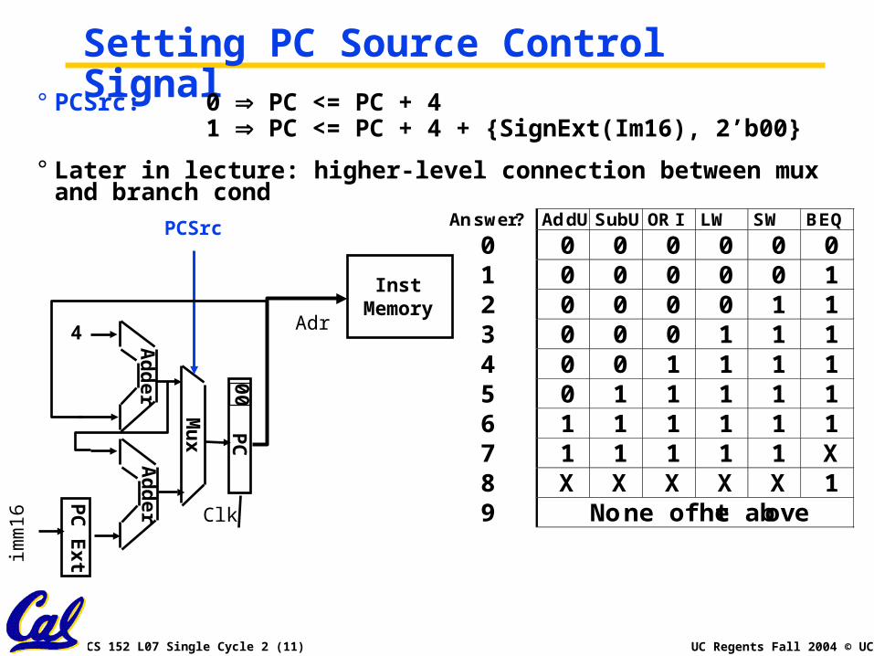
Setting PC Source Control Signal° PCSrc: 0 PC <= PC + 4
1 PC <= PC + 4 + {SignExt(Im16), 2’b00}
° Later in lecture: higher-level connection between mux and branch cond
Adr
InstMemory
Ad
der
Ad
der
PC
Clk
00
Mu
x
4
PCSrc
PC
Extim
m16
Answer? AddU SubU ORI LW SW BEQ
0 0 0 0 0 0 01 0 0 0 0 0 12 0 0 0 0 1 13 0 0 0 1 1 14 0 0 1 1 1 15 0 1 1 1 1 16 1 1 1 1 1 17 1 1 1 1 1 X8 X X X X X 19 None of the above

CS 152 L07 Single Cycle 2 (13) UC Regents Fall 2004 © UCB
Meaning of the Control Signals° ExtOp: 0 “zero” ; 1 “sign”
° ALUsrc: 0 regB; 1 immed
° ALUctr: “add”, “sub”, “or”
° MemWr: 1 write memory
° MemtoReg: 0 ALU; 1 Mem
° RegDst: 0 “rt”; 1 “rd”
° RegWr: 1 write register
32
ALUctr
Clk
busW
RegWr
32
32
busA
32
busB
55 5
Rw Ra Rb
32 32-bitRegisters
Rs
Rt
Rt
RdRegDst
Exten
der
Mu
x
3216imm16
ALUSrcExtOp
Mu
x
MemtoReg
Clk
Data InWrEn32 Adr
DataMemory
MemWr
AL
U
Zero
0
1
0
1
01

CS 152 L07 Single Cycle 2 (14) UC Regents Fall 2004 © UCB
Specify ALU source mux Control
° ALUsrc: 0 reg as ALU B input; 1 immediate as ALU B input
Clk
busW
32
32
busA
32
busB
55 5
Rw Ra Rb
32 32-bitRegisters
Rs
Rt
Rt
Rd
Exten
der
Mu
x
3216imm16
ALUSrcExtOp
Data In32
AL
U
0
1
01 Answer? AddU SubU ORI LW SW BEQ
0 0 0 0 0 0 01 0 0 0 0 0 12 0 0 0 0 1 13 0 0 1 1 1 04 0 0 0 1 1 15 0 0 0 1 1 X6 1 1 1 1 1 17 1 1 1 1 1 X8 X X X X X 19 None of the above

CS 152 L07 Single Cycle 2 (16) UC Regents Fall 2004 © UCB
Administrivia°COD Reading for next lecture: Sections 5.5 “Multicycle”, 5.6 “Microprogramming” (on CD), “Fallacies and Pitfalls” 5.10
°Start Homework #2
°Lab 2 Verilog simulation Friday
°Find bugs in COD 3rd Edition?• $1 reward to first person to report a bug
• Send email to [email protected] Include Page number, line number on page,
BEFORE with bug, AFTER fix, why it’s a bug
CS 152 L07 Single Cycle 2 (17) UC Regents Fall 2004 © UCB
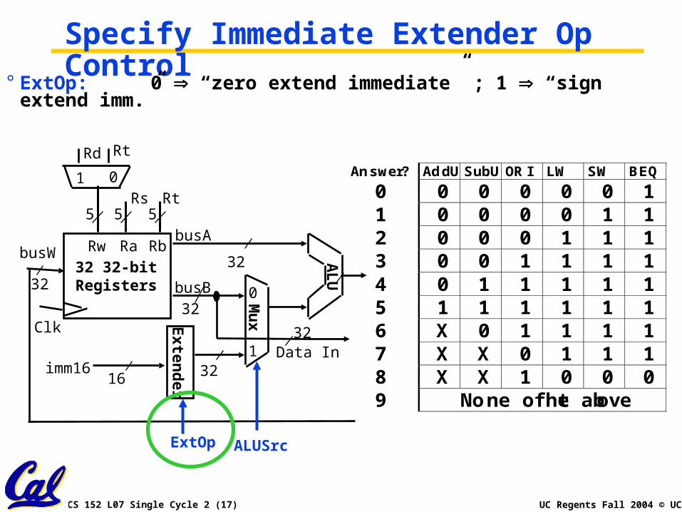
Specify Immediate Extender Op Control
° ExtOp: 0 “zero extend immediate” ; 1 “sign extend imm.”
Clk
busW
32
32
busA
32
busB
55 5
Rw Ra Rb
32 32-bitRegisters
Rs
Rt
Rt
Rd
Exten
der
Mu
x
3216imm16
ALUSrcExtOp
Data In32
AL
U
0
1
01 Answer? AddU SubU ORI LW SW BEQ
0 0 0 0 0 0 11 0 0 0 0 1 12 0 0 0 1 1 13 0 0 1 1 1 14 0 1 1 1 1 15 1 1 1 1 1 16 X 0 1 1 1 17 X X 0 1 1 18 X X 1 0 0 09 None of the above

CS 152 L07 Single Cycle 2 (19) UC Regents Fall 2004 © UCB
Specify Register Write Control
° RegWr: 1 write register
32
Clk
busW
RegWr
32
32
busA
32
busB
55 5
Rw Ra Rb
32 32-bitRegisters
Rs
Rt
Rt
RdRegDst
Exten
der
Mu
x
3216imm16
ALUSrcExtOp
AL
U
0
1
01
Answer? AddU SubU ORI LW SW BEQ
0 0 0 0 0 0 0 1 0 0 0 0 0 1 2 0 0 0 0 1 1 3 0 0 0 1 1 1 4 0 0 1 1 1 1 5 0 1 1 1 1 1 6 1 1 1 1 1 1 7 1 1 1 1 0 0 8 1 1 1 1 X X 9 None of the above
CS 152 L07 Single Cycle 2 (21) UC Regents Fall 2004 © UCB
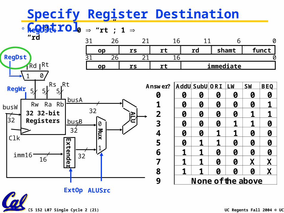
Specify Register Destination Control° RegDst: 0 “rt”; 1 “rd”
Clk
busW
RegWr
32
32
busA
32
busB
55 5
Rw Ra Rb
32 32-bitRegisters
Rs
Rt
Rt
RdRegDst
Exten
der
Mu
x
3216imm16
ALUSrcExtOp
AL
U
0
1
01
Answer? AddU SubU ORI LW SW BEQ
0 0 0 0 0 0 0 1 0 0 0 0 0 1 2 0 0 0 0 1 1 3 0 0 0 1 1 0 4 0 0 1 1 0 0 5 0 1 1 0 0 0 6 1 1 0 0 0 0 7 1 1 0 0 X X 8 1 1 0 0 0 X 9 None of the above
op rs rt immediate016212631
op rs rt rd shamt funct
061116212631

CS 152 L07 Single Cycle 2 (23) UC Regents Fall 2004 © UCB
Answer? AddU SubU ORI LW SW BEQ
0 0 0 0 0 0 0 1 0 0 0 0 0 1 2 0 0 0 0 1 0 3 0 0 0 1 0 0 4 0 0 1 0 0 0 5 0 1 0 0 0 0 6 1 0 0 0 0 0 7 0 0 0 0 1 X 8 X X X 0 1 X 9 None of the above
Specify the Memory Write Control Signal° MemWr: 1 write memory
busW
32
ALUctr
Clk
RegWr
32
32
busA
32busB
55 5
Rw Ra Rb32 32-bitRegisters
Rs
Rt
Rt
RdRegDst
Exten
der
Mu
x
3216imm16
ALUSrcExtOp
Mu
x
MemtoReg
Clk
Data InWrEn32 Adr
DataMemory
MemWr
AL
U
Zero
0
1
0
1
01
CS 152 L07 Single Cycle 2 (25) UC Regents Fall 2004 © UCB
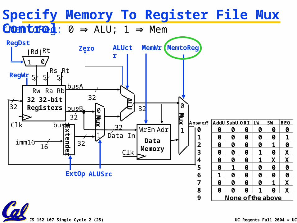
Specify Memory To Register File Mux Control° MemtoReg:0 ALU; 1 Mem
busW
32
ALUctr
Clk
RegWr
32
32
busA
32busB
55 5
Rw Ra Rb32 32-bitRegisters
Rs
Rt
Rt
RdRegDst
Exten
der
Mu
x
3216imm16
ALUSrcExtOp
Mu
x
MemtoReg
Clk
Data InWrEn32 Adr
DataMemory
MemWr
AL
U
Zero
0
1
0
1
01
Answer? AddU SubU ORI LW SW BEQ
0 0 0 0 0 0 0 1 0 0 0 0 0 1 2 0 0 0 0 1 0 3 0 0 0 1 0 X 4 0 0 0 1 X X 5 0 1 0 0 0 0 6 1 0 0 0 0 0 7 0 0 0 0 1 X 8 0 0 0 1 0 X 9 None of the above

CS 152 L07 Single Cycle 2 (27) UC Regents Fall 2004 © UCB
Specify the ALU Control Signals° ALUctr: 0 “add”, 1 “sub”, 2 “or”
Answer? AddU SubU ORI LW SW BEQ
0 0 0 0 0 0 01 0 0 0 0 0 12 0 1 0 0 0 13 0 1 2 0 0 14 0 1 2 0 0 X5 0 1 2 0 X X6 0 1 2 X X X7 X 1 2 X X X8 X X 2 0 0 19 None of the above
busW
32
ALUctr
Clk
RegWr
32
32
busA
32busB
55 5
Rw Ra Rb32 32-bitRegisters
Rs
Rt
Rt
RdRegDst
Exten
der
Mu
x
3216imm16
ALUSrcExtOp
Mu
x
MemtoReg
Clk
Data InWrEn32 Adr
DataMemory
MemWr
AL
U
Zero
0
1
0
1
01

CS 152 L07 Single Cycle 2 (29) UC Regents Fall 2004 © UCB
The Add Instruction
° add rd, rs, rt
• mem[PC] Fetch the instruction from memory
• R[rd] <= R[rs] + R[rt] The actual operation
• PC <= PC + 4 Calculate the next instruction’s
address
op rs rt rd shamt funct
061116212631
6 bits 6 bits5 bits5 bits5 bits5 bits

CS 152 L07 Single Cycle 2 (30) UC Regents Fall 2004 © UCB
Instruction Fetch Unit at the Beginning of Add° Fetch the instruction from Instruction memory:
Instruction <= mem[PC]• This is the same for all instructions
PC
Ext
Adr
InstMemory
Ad
der
Ad
der
PC
Clk
00
Mu
x4
PCSrc
imm
16
Instruction<31:0>

CS 152 L07 Single Cycle 2 (31) UC Regents Fall 2004 © UCB
Instruction Fetch Unit at the End of Branchif (Zero == 1) PC = PC + 4 + {SignExt[imm16], 2’b00} ;
else PC = PC + 4
op rs rt immediate
016212631
° What is encoding of PCSrc?• Direct MUX select?
• Branch / not branch
° Let’s choose second option
PCSrc zero? MUX0 X 01 0 01 1 1
Adr
InstMemory
Ad
der
Ad
der
PC
Clk
00
Mu
x
4
PCSrc
imm
16
Instruction<31:0>
0
1
Zero
PCSrc

CS 152 L07 Single Cycle 2 (32) UC Regents Fall 2004 © UCB
The Single Cycle Datapath during Load
32
ALUctr <= Add
Clk
busW
RegWr <= 1
32
32
busA
32
busB
55 5
Rw Ra Rb
32 32-bitRegisters
Rs
Rt
Rt
RdRegDst = 0
Exten
der
Mu
x
Mux
3216imm16
ALUSrc = 1
ExtOp <= 1
Mu
x
MemtoReg <= 1
Clk
Data InWrEn
32
Adr
DataMemory
32
MemWr = 0A
LU
InstructionFetch Unit
Clk
Zero
Instruction<31:0>
0
1
0
1
01<
21:25>
<16:20>
<11:15>
<0:15>
Imm16RdRsRt
° R[rt] <= Data Memory [R[rs] + SignExt[imm16]]
op rs rt immediate
016212631
PCSrc<= +4

CS 152 L07 Single Cycle 2 (33) UC Regents Fall 2004 © UCB
The Single Cycle Datapath during Store
° Data Memory [R[rs] + SignExt[imm16]] <= R[rt]
op rs rt immediate
016212631
32
ALUctr <=
Clk
busW
RegWr <=
32
32
busA
32
busB
55 5
Rw Ra Rb
32 32-bitRegisters
Rs
Rt
Rt
RdRegDst <=
Exten
der
Mu
x
Mux
3216imm16
ALUSrc <=
ExtOp <=
Mu
x
MemtoReg <=
Clk
Data InWrEn
32
Adr
DataMemory
32
MemWr <= A
LU
InstructionFetch Unit
Clk
Zero
Instruction<31:0>
0
1
0
1
01<
21:25>
<16:20>
<11:15>
<0:15>
Imm16RdRsRt
PCSrc <=

CS 152 L07 Single Cycle 2 (34) UC Regents Fall 2004 © UCB
The Single Cycle Datapath during Store
32
ALUctr <= Add
Clk
busW
RegWr <= 0
32
32
busA
32
busB
55 5
Rw Ra Rb
32 32-bitRegisters
Rs
Rt
Rt
RdRegDst <= x
Exten
der
Mu
x
Mux
3216imm16
ALUSrc <= 1
ExtOp <= 1
Mu
x
MemtoReg <= x
Clk
Data InWrEn
32Adr
DataMemory
32
MemWr <= 1A
LU
InstructionFetch Unit
Clk
Zero
Instruction<31:0>
0
1
0
1
01<
21:25>
<16:20>
<11:15>
<0:15>
Imm16RdRsRt
° Data Memory [R[rs] + SignExt[imm16]] <= R[rt]
op rs rt immediate
016212631
PCSrc<= +4

CS 152 L07 Single Cycle 2 (35) UC Regents Fall 2004 © UCB
The Single Cycle Datapath during Branch
32
ALUctr <=Sub
Clk
busW
RegWr <= 0
32
32
busA
32
busB
55 5
Rw Ra Rb
32 32-bitRegisters
Rs
Rt
Rt
RdRegDst <= x
Exten
der
Mu
x
Mux
3216imm16
ALUSrc <= 0
ExtOp <= x
Mu
x
MemtoReg <= x
Clk
Data InWrEn
32
Adr
DataMemory
32
MemWr <= 0A
LU
InstructionFetch Unit
Clk
Zero
Instruction<31:0>
0
1
0
1
01<
21:25>
<16:20>
<11:15>
<0:15>
Imm16RdRsRt
if (R[rs] - R[rt] == 0) Zero <= 1 ; else Zero <= 0op rs rt immediate
016212631
PCSrc<= “Br”

CS 152 L07 Single Cycle 2 (36) UC Regents Fall 2004 © UCB
Step 4: Given Datapath: RTL -> Control
ALUctrRegDst ALUSrcExtOp MemtoRegMemWr Zero
Instruction<31:0>
<21:25>
<16:20>
<11:15>
<0:15>
Imm16RdRsRt
PCSrc
Adr
InstMemory
DATA PATH
Control
Op
<21:25>
Fun
RegWr

CS 152 L07 Single Cycle 2 (37) UC Regents Fall 2004 © UCB
A Summary of Control Signals
inst Register Transfer
ADD R[rd] <= R[rs] + R[rt]; PC <= PC + 4
ALUsrc = RegB, ALUctr = “add”, RegDst = rd, RegWr, PCSrc = “+4”
SUB R[rd] <= R[rs] – R[rt]; PC <= PC + 4
ALUsrc = RegB, ALUctr = “sub”, RegDst = rd, RegWr, PCSrc = “+4”
ORi R[rt] <= R[rs] + zero_ext(Imm16); PC <= PC + 4
ALUsrc = Im, Extop = “Z”, ALUctr = “or”, RegDst = rt, RegWr, PCSrc = “+4”
LOAD R[rt] <= MEM[ R[rs] + sign_ext(Imm16)]; PC <= PC + 4
ALUsrc = Im, Extop = “Sn”, ALUctr = “add”, MemtoReg, RegDst = rt, RegWr, PCSrc = “+4”
STORE MEM[ R[rs] + sign_ext(Imm16)] <= R[rs]; PC <= PC + 4
ALUsrc = Im, Extop = “Sn”, ALUctr = “add”, MemWr, PCSrc = “+4”
BEQ if ( R[rs] == R[rt] ) then PC <= PC +4 + {sign_ext(Imm16)], 00’b2} else PC <= PC + 4
PCSrc = “Br”, ALUctr = “sub”

CS 152 L07 Single Cycle 2 (38) UC Regents Fall 2004 © UCB
A Summary of the Control Signals
add sub ori lw sw beq
RegDst
ALUSrc
MemtoReg
RegWrite
MemWrite
PCSrcExtOp
ALUctr<2:0>
1
0
0
1
0
0x
Add
1
0
0
1
0
0x
Subtract
0
1
0
1
0
00
Or
0
1
1
1
0
01
Add
x
1
x
0
1
01
Add
x
0
x
0
0
1x
Subtract
op target address
op rs rt rd shamt funct
061116212631
op rs rt immediate
R-type
I-type
J-type
add, sub
ori, lw, sw, beq
jump
func
op 00 0000 00 0000 00 1101 10 0011 10 1011 00 0100Appendix A10 0000See 10 0010 We Don’t Care :-)

CS 152 L07 Single Cycle 2 (39) UC Regents Fall 2004 © UCB
How to implement control in Verilog?°Need to set control lines based on instruction
°Which statement in Verilog good for doing different operations depending on value in a field of a word?
case (selector) item {, item} : statement;item {, item} : statement;default : statement
endcase

CS 152 L07 Single Cycle 2 (40) UC Regents Fall 2004 © UCB
The Single Cycle Datapath during Or Immediate
32
ALUctr <= Or
Clk
busW
RegWr <= 1
32
32
busA
32
busB
55 5
Rw Ra Rb
32 32-bitRegisters
Rs
Rt
Rt
RdRegDst <= 0
Exten
der
Mu
x
Mux
3216imm16
ALUSrc <= 1
ExtOp <= 0
Mu
x
MemtoReg <= 0
Clk
Data InWrEn
32
Adr
DataMemory
32
MemWr <= 0A
LU
InstructionFetch Unit
Clk
Zero
Instruction<31:0>
° R[rt] <= R[rs] or ZeroExt[Imm16]
0
1
0
1
01<
21:25>
<16:20>
<11:15>
<0:15>
Imm16RdRsRt
op rs rt immediate
016212631
PCSrc <= +4

CS 152 L07 Single Cycle 2 (41) UC Regents Fall 2004 © UCB
Example for OR immediate casecase (Instruction<31:25>) 13 /* ORi */ :
beginRegDst = 0; ALUSrc = 1; MemtoReg = 0; RegWrite = 1; MemWrite = 0; PCSrc = 0; ExtOp = 0; ALUctr = 2’b10;
end…default : statement
endcase

CS 152 L07 Single Cycle 2 (42) UC Regents Fall 2004 © UCB
Specify all control in one assignmentcase (Instruction<31:25>) 13 /* ORi */ :
{RegDst,ALUSrc,MemtoReg, RegWrite,MemWrite,PCSrc,Jump,
ExtOp,ALUctr} = {1’b0, 1’b1, 1’b0, 1’b1,
1’b0, 1’b0, 1’b0, 2’b01}; …
default : statement
endcase

CS 152 L07 Single Cycle 2 (43) UC Regents Fall 2004 © UCB
Better way than specify as 0s and 1s°Hard to read and understand
• Easy to make mistakes; Alternative?
°Associate Names with control values!
parameter RegDstRt=0, RegDstRd=1,ALUSrcBReg = 0, ALUSrcBImm = 1, RegValALU = 0, RegValMem = 1, RegWr = 1, NoRegWr = 0,MemWr = 1, NoMemWr = 0,PCSrc4 = 0, PCSrcBr = 1,ZeroExt = 0, SignExt = 1,Add = 0, Sub = 1, Or = 2;

CS 152 L07 Single Cycle 2 (44) UC Regents Fall 2004 © UCB
Specify all control symbolicallycase (Instruction<31:25>)
13 /* ORi */ :
{RegDst,ALUSrc,MemtoReg, RegWrite,MemWrite,PCSrc,Jump, ExtOp,ALUctr} = {RegDstRt, ALUSrcBImm, RegValALU, RegWr, NoMemWr, PCSrc4, ZeroExt, Or};
… default : statement
endcase

CS 152 L07 Single Cycle 2 (45) UC Regents Fall 2004 © UCB
Local Decoding: R-type v. Add + Sub
R-type ori lw sw beq
RegDst
ALUSrc
MemtoReg
RegWrite
MemWrite
Branch
Jump
ExtOp
ALUop<N:0>
1
0
0
1
0
0
0
x
“R-type”
0
1
0
1
0
0
0
0
Or
0
1
1
1
0
0
0
1
Add
x
1
x
0
1
0
0
1
Add
x
0
x
0
0
1
0
x
Subtract
op 00 0000 00 1101 10 0011 10 1011 00 0100
MainControl
op
6
ALUControl(Local)
func
N
6ALUop
ALUctr
3
AL
U
CS 152 L07 Single Cycle 2 (46) UC Regents Fall 2004 © UCB
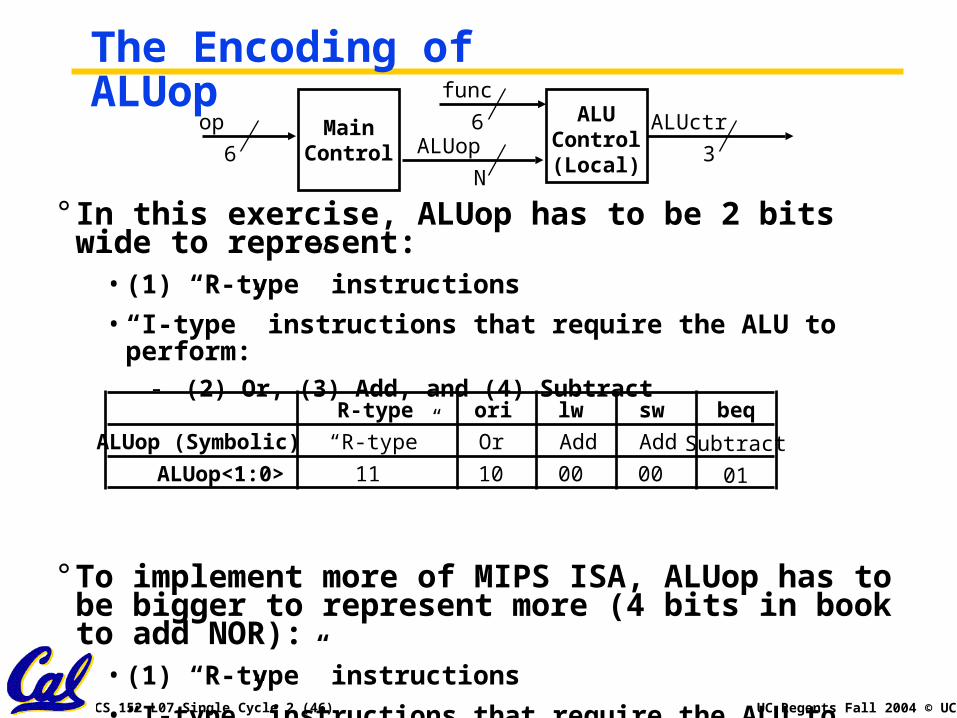
The Encoding of ALUop
° In this exercise, ALUop has to be 2 bits wide to represent:
• (1) “R-type” instructions
• “I-type” instructions that require the ALU to perform:- (2) Or, (3) Add, and (4) Subtract
° To implement more of MIPS ISA, ALUop has to be bigger to represent more (4 bits in book to add NOR):
• (1) “R-type” instructions
• “I-type” instructions that require the ALU to perform:- (2) Or, (3) Add, (4) Subtract, and (5) Nor (Example: nor)
MainControl
op
6
ALUControl(Local)
func
N
6ALUop
ALUctr
3
R-type ori lw sw beq
ALUop (Symbolic) “R-type” Or Add Add Subtract
ALUop<1:0> 11 10 00 00 01

CS 152 L07 Single Cycle 2 (47) UC Regents Fall 2004 © UCB
Drawback of this Single Cycle Processor°Long cycle time:• Cycle time must be long enough for the load instruction:
PC’s Clock -to-Q +
Instruction Memory Access Time +
Register File Access Time +
ALU Delay (address calculation) +
Data Memory Access Time +
Register File Setup Time +
Clock Skew
°Cycle time for load is much longer than needed for all other instructions

CS 152 L07 Single Cycle 2 (48) UC Regents Fall 2004 © UCB
PreviewNext Time:
°MultiCycle Data Path•CPI 1, CycleTime much shorter (~1/5 of time)

CS 152 L07 Single Cycle 2 (49) UC Regents Fall 2004 © UCB
° Single cycle datapath => CPI=1, CCT => long
° 5 steps to design a processor• 1. Analyze instruction set => datapath requirements
• 2. Select set of datapath components & establish clock methodology
• 3. Assemble datapath meeting the requirements
• 4. Analyze implementation of each instruction to determine setting of control points that effects the register transfer.
• 5. Assemble the control logic
° Control is the hard part
° MIPS makes control easier• Instructions same size
• Source registers always in same place
• Immediates same size, location
• Operations always on registers/immediates
Summary
Control
Datapath
Memory
ProcessorInput
Output

CS 152 L07 Single Cycle 2 (50) UC Regents Fall 2004 © UCB
Where to get more information?
° Chapter 5.1 to 5.4 of your text book:• David Patterson and John Hennessy, “Computer
Organization & Design: The Hardware / Software Interface,” Third Edition, Morgan Kaufman Publishers, San Mateo, California, 2003.
° One of the best PhD thesis on processor design:
• Manolis Katevenis, “Reduced Instruction Set Computer Architecture for VLSI,” PhD Dissertation, EECS, U C Berkeley, 1982.
° For a reference on the MIPS architecture:• Gerry Kane, Joe Heinrich “MIPS RISC
Architecture,” Prentice Hall, 2nd edition, 1992

CS 152 L07 Single Cycle 2 (51) UC Regents Fall 2004 © UCB
Bonus Slides°The following slides show how to go from tables that describe inputs and control lines into gates
°Can be done by CAD tools instead of by hand for 2-level logic equations very efficiently
CS 152 L07 Single Cycle 2 (52) UC Regents Fall 2004 © UCB
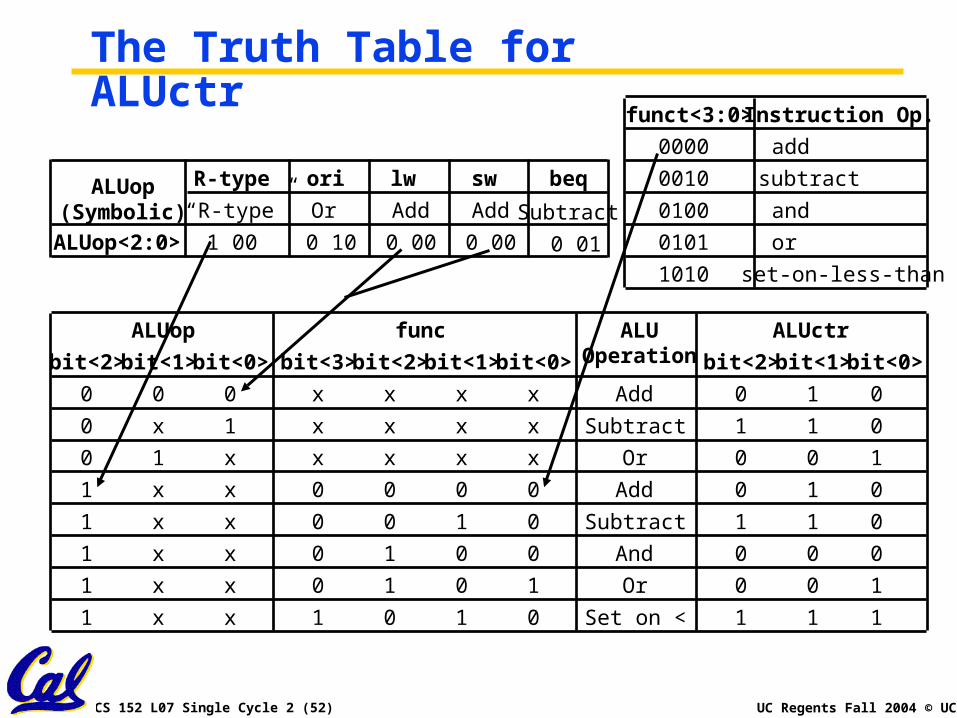
The Truth Table for ALUctr
R-type ori lw sw beqALUop(Symbolic) “R-type” Or Add Add Subtract
ALUop<2:0> 1 00 0 10 0 00 0 00 0 01
ALUop func
bit<2> bit<1> bit<0> bit<2> bit<1> bit<0>bit<3>
0 0 0 x x x x
ALUctrALUOperation
Add 0 1 0
bit<2> bit<1> bit<0>
0 x 1 x x x x Subtract 1 1 0
0 1 x x x x x Or 0 0 1
1 x x 0 0 0 0 Add 0 1 0
1 x x 0 0 1 0 Subtract 1 1 0
1 x x 0 1 0 0 And 0 0 0
1 x x 0 1 0 1 Or 0 0 1
1 x x 1 0 1 0 Set on < 1 1 1
funct<3:0> Instruction Op.
0000
0010
0100
0101
1010
add
subtract
and
or
set-on-less-than

CS 152 L07 Single Cycle 2 (53) UC Regents Fall 2004 © UCB
The Logic Equation for ALUctr<2>ALUop func
bit<2> bit<1> bit<0> bit<2> bit<1> bit<0>bit<3> ALUctr<2>
0 x 1 x x x x 1
1 x x 0 0 1 0 1
1 x x 1 0 1 0 1
° (ALUctr<2> = ! ALUop<2>) & ALUop<0> + ALUop<2> & !func<2> & func<1> & !
func<0>
This makes func<3> a don’t care

CS 152 L07 Single Cycle 2 (54) UC Regents Fall 2004 © UCB
The Logic Equation for ALUctr<1>
ALUop func
bit<2> bit<1> bit<0> bit<2> bit<1> bit<0>bit<3>
0 0 0 x x x x 1
ALUctr<1>
0 x 1 x x x x 1
1 x x 0 0 0 0 1
1 x x 0 0 1 0 1
1 x x 1 0 1 0 1
° (ALUctr<1> = !ALUop<2>) & !ALUop<1> + ALUop<2> & !func<2> & !func<0>

CS 152 L07 Single Cycle 2 (55) UC Regents Fall 2004 © UCB
The Logic Equation for ALUctr<0>
ALUop func
bit<2> bit<1> bit<0> bit<2> bit<1> bit<0>bit<3> ALUctr<0>
0 1 x x x x x 1
1 x x 0 1 0 1 1
1 x x 1 0 1 0 1
° ALUctr<0> = !ALUop<2> & ALUop<1> + ALUop<2> & !func<3> & func<2>
& !func<1> & func<0>
+ ALUop<2> & func<3> & !func<2> & func<1> & !func<0>
CS 152 L07 Single Cycle 2 (56) UC Regents Fall 2004 © UCB
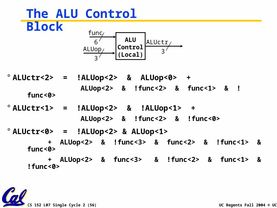
The ALU Control Block
ALUControl(Local)
func
3
6ALUop
ALUctr
3
° ALUctr<2> = !ALUop<2> & ALUop<0> + ALUop<2> & !func<2> & func<1> & !func<0>
° ALUctr<1> = !ALUop<2> & !ALUop<1> + ALUop<2> & !func<2> & !func<0>
° ALUctr<0> = !ALUop<2> & ALUop<1> + ALUop<2> & !func<3> & func<2> & !func<1> &
func<0>
+ ALUop<2> & func<3> & !func<2> & func<1> & !func<0>

CS 152 L07 Single Cycle 2 (57) UC Regents Fall 2004 © UCB
Step 5: Logic for each control signal
° PCSrc <= (OP == `BEQ) ? `Br : `plus4;
° ALUsrc <= (OP == `Rtype) ? `regB : `immed;
° ALUctr <= (OP == `Rtype`) ? funct :(OP == `ORi) ? `ORfunction :(OP == `BEQ) ? `SUBfunction :
`ADDfunction;
° ExtOp <= _____________
° MemWr <= _____________
° MemtoReg <= _____________
° RegWr: <=_____________
° RegDst: <= _____________

CS 152 L07 Single Cycle 2 (58) UC Regents Fall 2004 © UCB
Step 5: Logic for each control signal
° PCSrc <= (OP == `BEQ) ? `Br : `plus4;
° ALUsrc <= (OP == `Rtype) ? `regB : `immed;
° ALUctr <= (OP == `Rtype`) ? funct :(OP == `ORi) ? `ORfunction :
(OP == `BEQ) ? `SUBfunction : `ADDfunction;
° ExtOp <= (OP == `ORi) : `ZEROextend : `SIGNextend;
° MemWr <= (OP == `Store) ? 1 : 0;
° MemtoReg <= (OP == `Load) ? 1 : 0;
° RegWr: <= ((OP == `Store) || (OP == `BEQ)) ? 0 : 1;
° RegDst: <= ((OP == `Load) || (OP == `ORi)) ? 0 : 1;

CS 152 L07 Single Cycle 2 (59) UC Regents Fall 2004 © UCB
The “Truth Table” for the Main Control
R-type ori lw sw beq jump
RegDst
ALUSrc
MemtoReg
RegWrite
MemWrite
PCSrc
Jump
ExtOp
ALUop (Symbolic)
1
0
0
1
0
0
0
x
“R-type”
0
1
0
1
0
0
0
0
Or
0
1
1
1
0
0
0
1
Add
x
1
x
0
1
0
0
1
Add
x
0
x
0
0
1
0
x
Subtract
x
x
x
0
0
0
1
x
xxx
op 00 0000 00 1101 10 0011 10 1011 00 0100 00 0010
ALUop <2> 1 0 0 0 0 x
ALUop <1> 0 1 0 0 0 x
ALUop <0> 0 0 0 0 1 x
MainControl
op
6
ALUControl(Local)
func
3
6
ALUop
ALUctr
3
RegDst
ALUSrc
:
CS 152 L07 Single Cycle 2 (60) UC Regents Fall 2004 © UCB
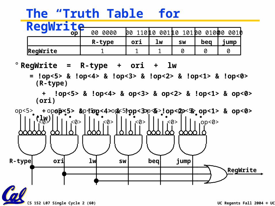
The “Truth Table” for RegWrite
R-type ori lw sw beq jump
RegWrite 1 1 1 0 0 0
op 00 0000 00 1101 10 0011 10 1011 00 0100 00 0010
° RegWrite = R-type + ori + lw= !op<5> & !op<4> & !op<3> & !op<2> & !op<1> & !op<0> (R-type)
+ !op<5> & !op<4> & op<3> & op<2> & !op<1> & op<0> (ori)
+ op<5> & !op<4> & !op<3> & !op<2> & op<1> & op<0> (lw)
op<0>
op<5>. .op<5>. .<0>
op<5>. .<0>
op<5>. .<0>
op<5>. .<0>
op<5>. .<0>
R-type ori lw sw beq jump
RegWrite

CS 152 L07 Single Cycle 2 (61) UC Regents Fall 2004 © UCB
PLA Implementation of the Main Control
op<0>
op<5>. .op<5>. .<0>
op<5>. .<0>
op<5>. .<0>
op<5>. .<0>
op<5>. .<0>
R-type ori lw sw beq jumpRegWrite
ALUSrc
MemtoReg
MemWrite
Branch
Jump
RegDst
ExtOp
ALUop<2>
ALUop<1>
ALUop<0>

CS 152 L07 Single Cycle 2 (62) UC Regents Fall 2004 © UCB
A Real MIPS Datapath (CNS T0)

CS 152 L07 Single Cycle 2 (63) UC Regents Fall 2004 © UCB
Putting it All Together: A Single Cycle Processor
32
ALUctr
Clk
busW
RegWr
32
32
busA
32
busB
55 5
Rw Ra Rb
32 32-bitRegisters
Rs
Rt
Rt
RdRegDst
Exten
der
Mu
x
Mux
3216imm16
ALUSrc
ExtOp
Mu
x
MemtoReg
Clk
Data InWrEn
32
Adr
DataMemory
32
MemWrA
LU
InstructionFetch Unit
Clk
Zero
Instruction<31:0>
0
1
0
1
01<
21:25>
<16:20>
<11:15>
<0:15>
Imm16RdRsRt
MainControl
op
6
ALUControlfunc
6
3
ALUopALUctr
3RegDst
ALUSrc
:Instr<5:0>
Instr<31:26>
Instr<15:0>
PCSrc