Embed Size (px)
Citation preview

CS 151
Digital Systems Design
Lecture 26
Shift Registers

Overview
° Multiple flip flops can be combined to form a data register
° Shift registers allow data to be transported one bit at a time
° Registers also allow for parallel transfer • Many bits transferred at the same time
° Shift registers can be used with adders to build arithmetic units
° Remember: most digital hardware can be built from combinational logic (and, or, invert) and flip flops• Basic components of most computers

Register with Parallel Load
° Register: Group of Flip-Flops
° Ex: D Flip-Flops
° Holds a Word (Nibble) of Data
° Loads in Parallel on ClockTransition
° Asynchronous Clear (Reset)
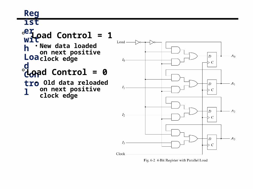
Register with Load Control
° Load Control = 1• New data loaded
on next positiveclock edge
° Load Control = 0• Old data reloaded
on next positiveclock edge
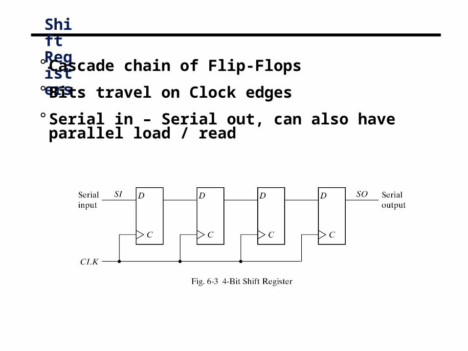
Shift Registers
° Cascade chain of Flip-Flops
° Bits travel on Clock edges
° Serial in – Serial out, can also have parallel load / read
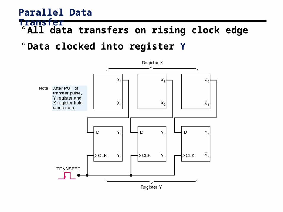
Parallel Data Transfer° All data transfers on rising clock edge
° Data clocked into register Y

Parallel versus Serial
° Serial communications is defined as • Provides a binary number as a sequence of binary digits, one
after another, through one data line.
° Parallel communications • Provides a binary number through multiple data lines at the
same time.

parallel inputs
parallel outputs
serial transmission
Shift register application
° Parallel-to-serial conversion for serial transmission

Serial Transfer
° Data transfer one bit at a time
° Data loopback for register A
Time
T0
T1
T2
T3
T4
Reg A
1011
1101
1110
0111
1011
Reg B
0011
1001
1100
0110
1011
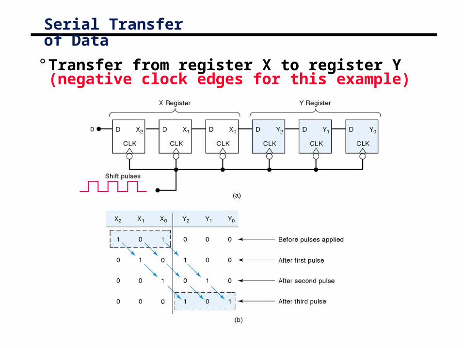
Serial Transfer of Data
° Transfer from register X to register Y (negative clock edges for this example)

D Q D Q D Q D QIN
OUT1 OUT2 OUT3 OUT4
CLK
OUT
Pattern recognizer
° Combinational function of input samples• in this case, recognizing the pattern 1001 on the single input
signal
Clk IN OUT1 OUT2 OUT3 OUT4 OUTBefore
1 1 0 0 0 0 0 2 0 1 0 0 0 0 3 0 0 1 0 0 0 4 1 0 0 1 0 0 5 0 1 0 0 1 1

Serial Addition (D Flip-Flop)
° Slower than parallel
° Low cost
° Share fasthardware onslow data
° Good for multiplexed data
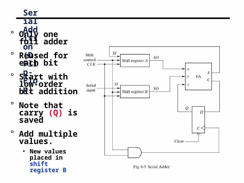
Serial Addition (D Flip-Flop)
° Only one full adder
° Reused for each bit
° Start with low-order bit addition
° Note that carry (Q) is saved
° Add multiple values.• New values
placed in shift register B

Serial Addition (D Flip-Flop)
° Shift control used to stop addition
° Generally not a good idea to gate the clock
° Shift register can be arbitrary length
° FA can be built from combin. logic

Universal Shift Register
° Clear
° Clock
° Shift
• Right
• Left
° Load
° Read
° Control
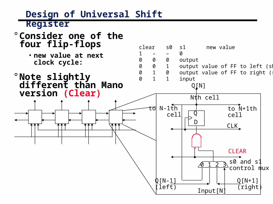
Nth cell
s0 and s1control mux0 1 2 3
D
Q
CLK
CLEAR
Q[N-1](left)
Q[N+1](right)
Input[N]
to N-1th cell
to N+1th cell
clears0 s1 new value1 – – 00 0 0 output0 0 1 output value of FF to left (shift right)0 1 0 output value of FF to right (shift left)0 1 1 input
Design of Universal Shift Register
° Consider one of the four flip-flops• new value at next clock
cycle:
° Note slightly different than Mano version (Clear)
Q[N]
Summary
° Shift registers can be combined together to allow for data transfer
° Serial transfer used in modems and computer peripherals (e.g. mouse)
° D flip flops allow for a simple design• Data clocked in during clock transition (rising or falling edge)
° Serial addition takes less chip area but is slow
° Universal shift register allows for many operations• The register is programmable.
• It allows for different operations at different times
° Next time: counters (circuits that count!)