Embed Size (px)
Citation preview
14-Aug-15 1
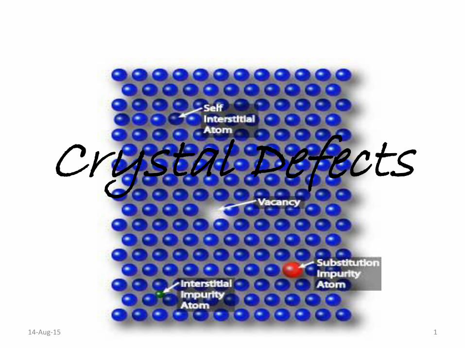
Crystal Defects
2
Defects in Solids There is no such thing as a perfect crystal.
• What are these Defects?
• Why are they important?
• Many of the important properties of materials are due
to the presence of imperfections.
• The properties of some materials are profoundly
influenced by the presence of imperfections.
• It is important to have knowledge about the types of
imperfections that exist and the roles they play in
affecting the behavior of materials.
3
Atom Purity and Crystal
Perfection
• Anything that deviated from this concept or intruded in
this uniform homogeneity would be an imperfection.
1. There are no perfect crystals.
2. Many material properties are improved by the
presence of imperfections and deliberately
modified (alloying and doping).
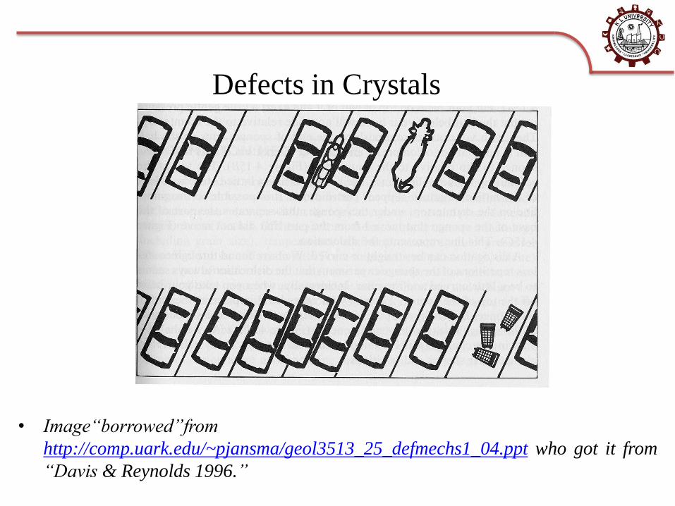
• Image“borrowed”from
http://comp.uark.edu/~pjansma/geol3513_25_defmechs1_04.ppt who got it from
“Davis & Reynolds 1996.”
Defects in Crystals
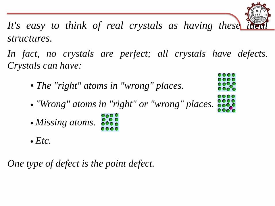
It's easy to think of real crystals as having these ideal
structures.
In fact, no crystals are perfect; all crystals have defects.
Crystals can have:
• The "right" atoms in "wrong" places.
• "Wrong" atoms in "right" or "wrong" places.
• Missing atoms.
• Etc.
One type of defect is the point defect.
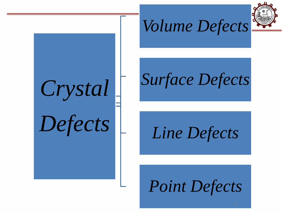
Crystal
Defects
Point Defects
Line Defects
Surface Defects
Volume Defects
6
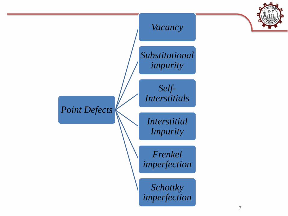
Point Defects
Vacancy
Substitutional impurity
Self-Interstitials
Interstitial Impurity
Frenkel imperfection
Schottky imperfection
7
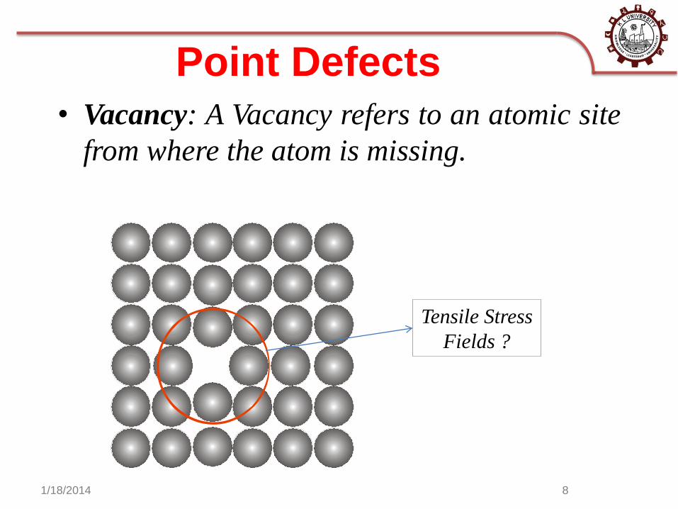
Point Defects • Vacancy: A Vacancy refers to an atomic site
from where the atom is missing.
Tensile Stress
Fields ?
1/18/2014 8
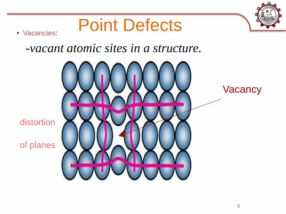
9
• Vacancies:
-vacant atomic sites in a structure.
Point Defects
Vacancy
distortion
of planes
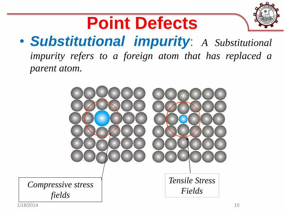
Point Defects • Substitutional impurity: A Substitutional
impurity refers to a foreign atom that has replaced a
parent atom.
Tensile Stress
Fields Compressive stress
fields 1/18/2014 10
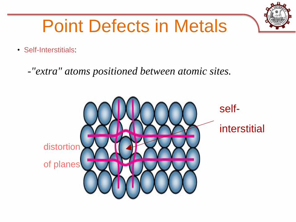
• Self-Interstitials:
-"extra" atoms positioned between atomic sites.
Point Defects in Metals
self-
interstitial
distortion
of planes
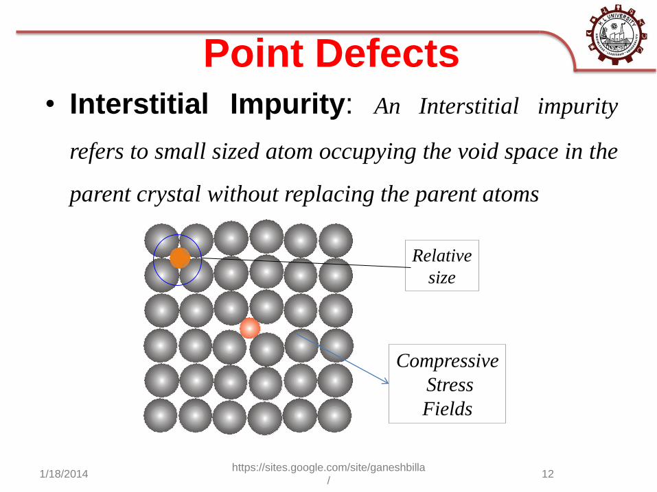
Point Defects • Interstitial Impurity: An Interstitial impurity
refers to small sized atom occupying the void space in the
parent crystal without replacing the parent atoms
Compressive
Stress
Fields
Relative
size
1/18/2014 12 https://sites.google.com/site/ganeshbilla
/
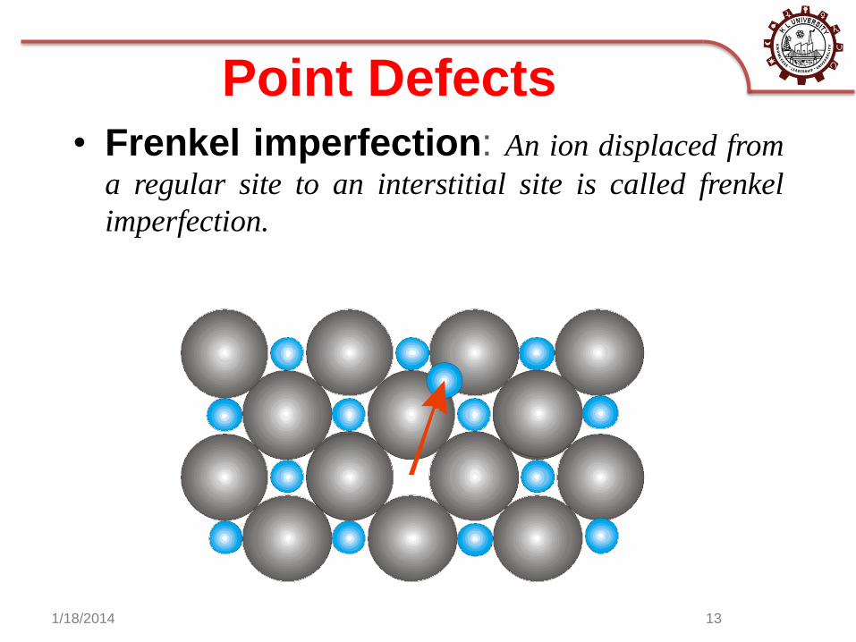
Point Defects • Frenkel imperfection: An ion displaced from
a regular site to an interstitial site is called frenkel
imperfection.
1/18/2014 13
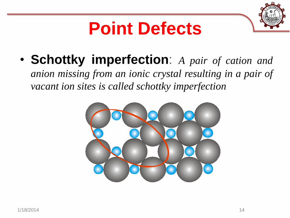
Point Defects
• Schottky imperfection: A pair of cation and
anion missing from an ionic crystal resulting in a pair of
vacant ion sites is called schottky imperfection
1/18/2014 14
Point Defects
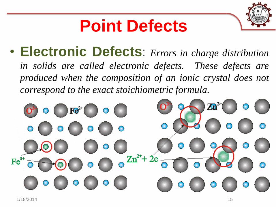
• Electronic Defects: Errors in charge distribution
in solids are called electronic defects. These defects are
produced when the composition of an ionic crystal does not
correspond to the exact stoichiometric formula.
1/18/2014 15
Line Defects • These are one dimensional imperfections in the
geometrical sense.
• These are also known as linear defects or Dislocations.
• Dislocations are areas were the atoms are out of position
in the crystal structure.
• These are generated when stress is applied.
• The motion of dislocations allows slip – plastic
deformation to occur.
1/18/2014 16
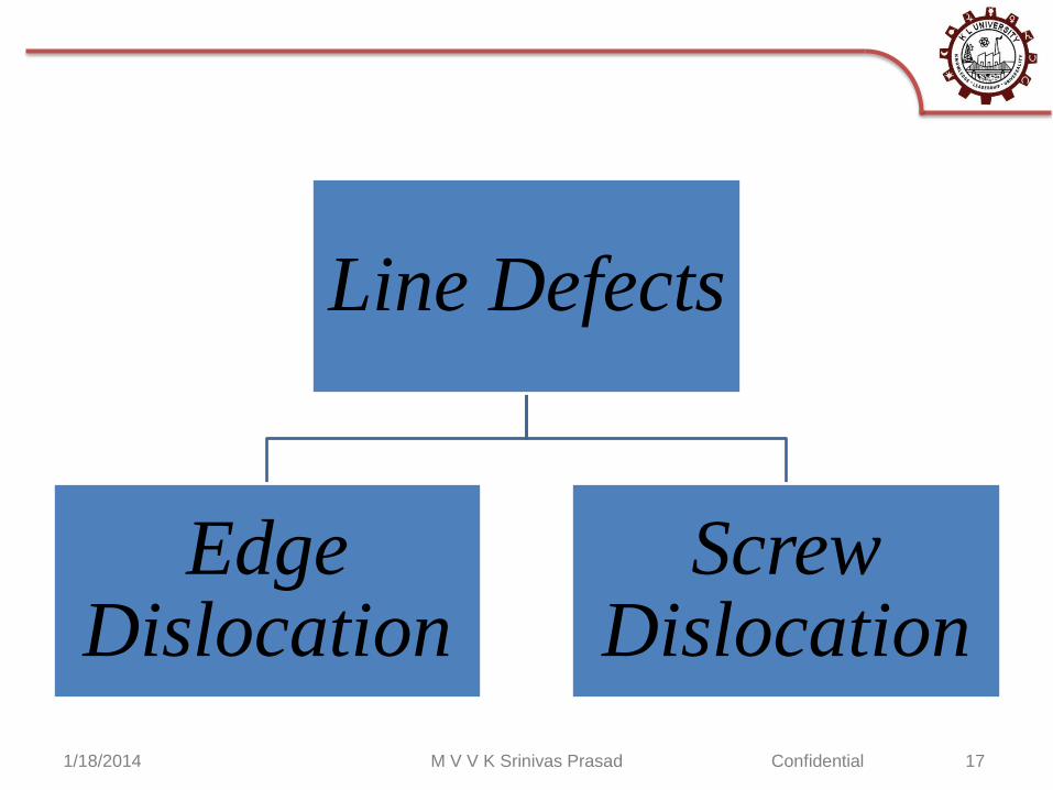
Line Defects
Edge Dislocation
Screw Dislocation
1/18/2014 M V V K Srinivas Prasad Confidential 17
Edge Dislocation
• In perfect crystal atoms are arranged in both vertical and
horizontal planes parallel to the side faces.
• If one of these planes does not extend to the full length but
ends in between within the crystal it is called edge
dislocation.
• Edge dislocation are caused by the termination of a plane
of atoms in the middle of the crystal.
1/18/2014 18
19
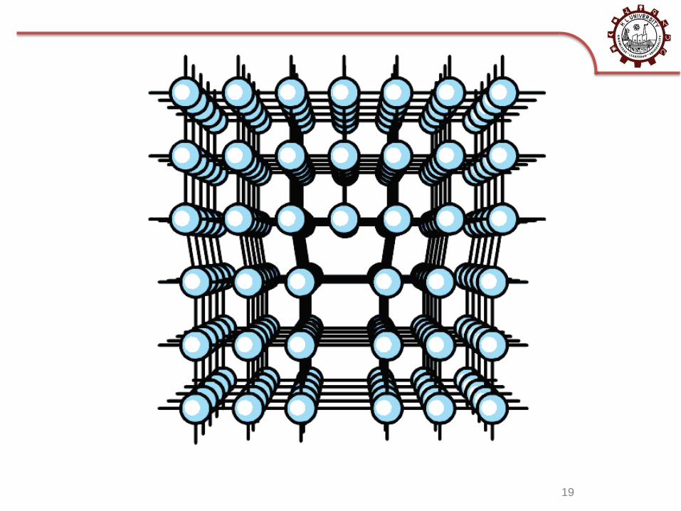
• Edge dislocation moves parallel to the direction of
stress.
• It can be easily visualized as an extra half-plane of
atoms in a lattice.
• The locus of defective points produced in the lattice by
the dislocation lie along a line.
• The inter-atomic bonds are significantly distorted only
in the immediate vicinity of the dislocation line.
20
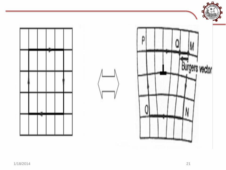
1/18/2014 21
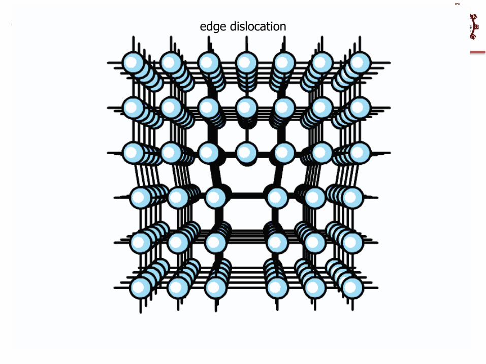
edge dislocation
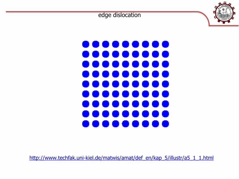
edge dislocation
http://www.techfak.uni-kiel.de/matwis/amat/def_en/kap_5/illustr/a5_1_1.html
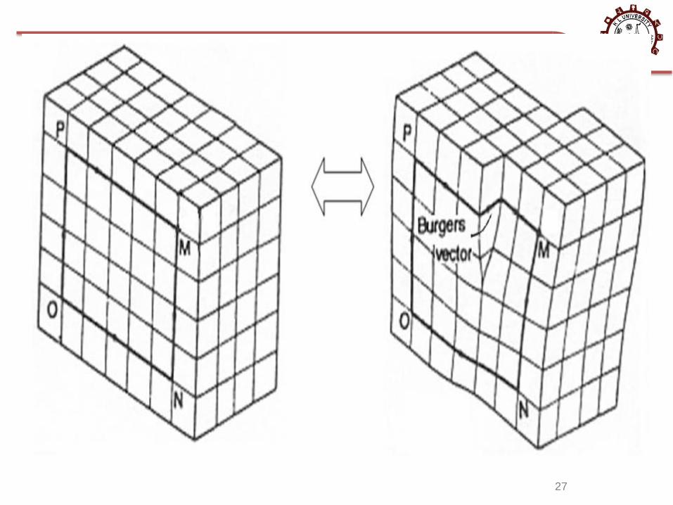
Screw Dislocation
• It results from a displacement of the atoms in one part of
a crystal relative to the rest of the crystal forming a spiral
ramp around the dislocation line.
• The motion of a screw dislocation is a result of shear
stress.
• But the defect line movement is perpendicular to direction
of the stress and the atom displacement, rather than
parallel.
1/18/2014 24
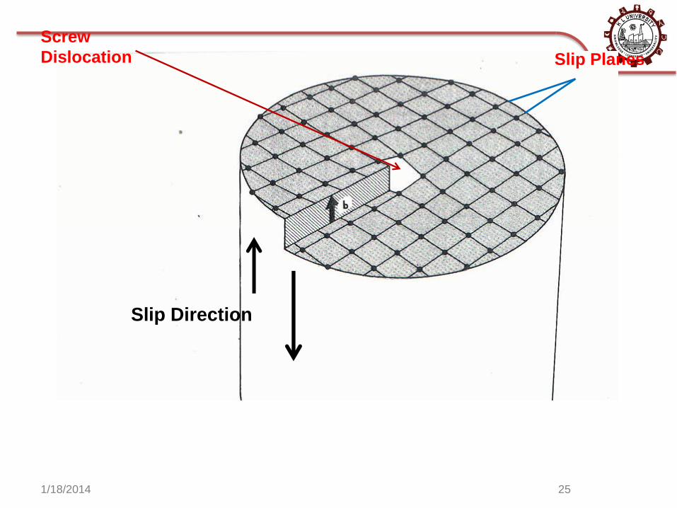
Screw
Dislocation Slip Planes
Slip Direction
1/18/2014 25
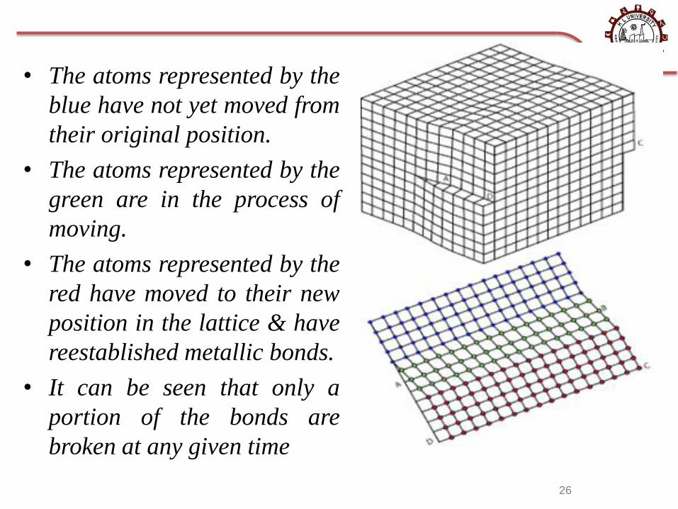
• The atoms represented by the
blue have not yet moved from
their original position.
• The atoms represented by the
green are in the process of
moving.
• The atoms represented by the
red have moved to their new
position in the lattice & have
reestablished metallic bonds.
• It can be seen that only a
portion of the bonds are
broken at any given time
26
27
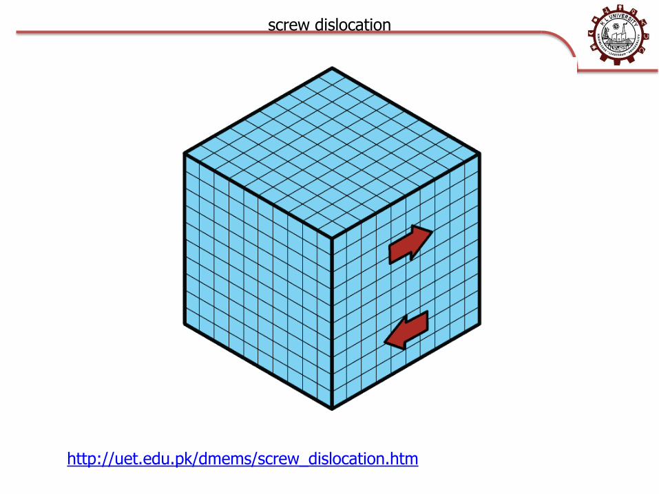
screw dislocation
http://uet.edu.pk/dmems/screw_dislocation.htm
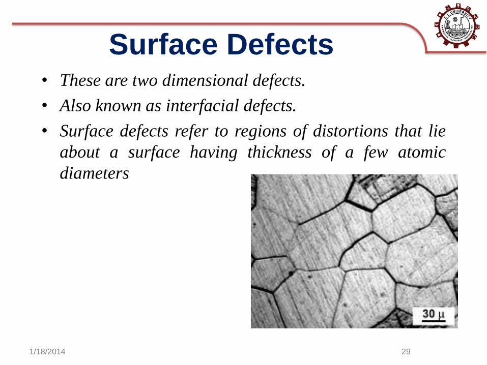
Surface Defects • These are two dimensional defects.
• Also known as interfacial defects.
• Surface defects refer to regions of distortions that lie
about a surface having thickness of a few atomic
diameters
1/18/2014 29
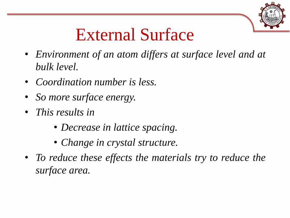
• Environment of an atom differs at surface level and at
bulk level.
• Coordination number is less.
• So more surface energy.
• This results in
• Decrease in lattice spacing.
• Change in crystal structure.
• To reduce these effects the materials try to reduce the
surface area.
External Surface
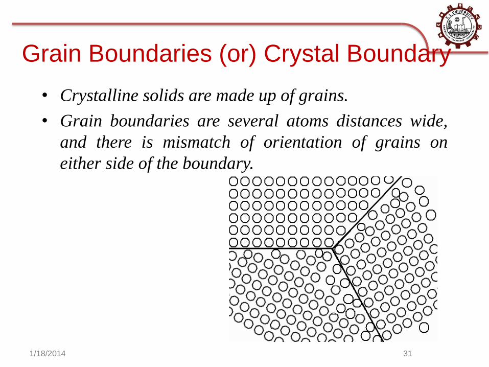
• Crystalline solids are made up of grains.
• Grain boundaries are several atoms distances wide,
and there is mismatch of orientation of grains on
either side of the boundary.
1/18/2014 31
Grain Boundaries (or) Crystal Boundary
Grain Boundaries
• When the orientation difference between two crystals
is less than 10° it is called low angle boundaries.
• If the low grain boundary is formed by edge
dislocations, it is called tilt boundary, and twist
boundary if formed of screw dislocations.
• The orientation difference is usually greater than 10-
15°. For this reason the grain boundaries are also
known as high angle boundaries.
• Grain boundaries are chemically more reactive
because of grain boundary energy.
1/18/2014 32
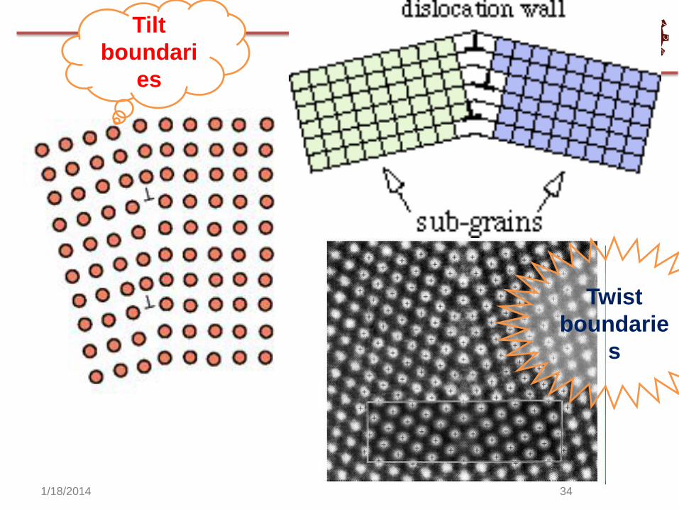
Grain Boundaries • The sub grain boundaries are of two types they are
• Tilt boundaries
• Twist boundaries
• An array of edge dislocations is called tilt boundary.
• A cross grid of screw dislocation is called twist
boundaries.
• A twin boundary happens when the crystals on either
side of a plane are mirror images of each other.
1/18/2014 33
1/18/2014 34
Tilt
boundari
es
Twist
boundarie
s
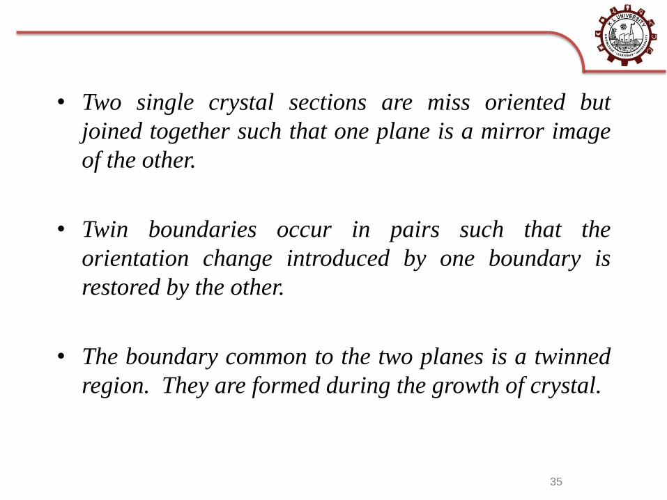
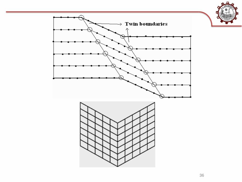
• Two single crystal sections are miss oriented but
joined together such that one plane is a mirror image
of the other.
• Twin boundaries occur in pairs such that the
orientation change introduced by one boundary is
restored by the other.
• The boundary common to the two planes is a twinned
region. They are formed during the growth of crystal.
35
36
• Twins which forms during the process of
recrystallization are called annealing twins,
• Twins which are formed during plastic deformation
are called deformation twins.
• Twinning occurs on a definite crystallographic plane
and in a specific direction, both of which depend on
the crystal structure.
• Annealing twins are typically found in metals that
have FCC crystal structure.
• While mechanical/deformation twins are observed in
BCC and HCP metals.
• Annealing twins are usually broader and with
straighter sides than mechanical twins.
• Twins do not extend beyond a grain boundary. 37
Stacking Defects • Stacking faults are planar surface imperfections caused by
fault in the staking sequence of atomic planes in crystals
• In FCC crystal we have three different stacking layers ABC
while in HCP stacking we have only two different layers
BC hence when FCC crystal grows we have the stacking
as ………ABCABCABCABC……
• While growing if the plane A indicated by arrow above
missing then we get the sequence
• ………ABCABCBCABC……
• Thus we find that the stacking in the missing region be
comes HCP. This thin region is a surface imperfection and
is called a stocking fault.
1/18/2014 38
Volume Defects
• Presence of a large vacancy (crakes) or void such as
clusters of atoms missing is also considered as a volume
defect. While crystal is grown there is every possibility of
inclusion of non-crystalline regions of dimensions of at
least 10 to 30°A. This is also called Volume imperfection.
1/18/2014 39


![Circular [35] 9 Muharram 1441 9 September 2019 DEVIATED ... · Pg. 1 of 5 Circular [35] 9 Muharram 1441 – 9 September 2019 DEVIATED SERIES (5) LAKEFIELD-BENONI MASJID – THEY DO](https://img.pdfslide.us/doc/110x75/602e50b7159338136b5ccc76/circular-35-9-muharram-1441-9-september-2019-deviated-pg-1-of-5-circular.jpg)